WO2021210593A1 - 赤外線センシングデバイス及びそれに用いる抵抗可変膜 - Google Patents
赤外線センシングデバイス及びそれに用いる抵抗可変膜 Download PDFInfo
- Publication number
- WO2021210593A1 WO2021210593A1 PCT/JP2021/015365 JP2021015365W WO2021210593A1 WO 2021210593 A1 WO2021210593 A1 WO 2021210593A1 JP 2021015365 W JP2021015365 W JP 2021015365W WO 2021210593 A1 WO2021210593 A1 WO 2021210593A1
- Authority
- WO
- WIPO (PCT)
- Prior art keywords
- infrared
- irradiation
- variable resistance
- resistance
- variable
- Prior art date
- Legal status (The legal status is an assumption and is not a legal conclusion. Google has not performed a legal analysis and makes no representation as to the accuracy of the status listed.)
- Ceased
Links
Images


Classifications
-
- H—ELECTRICITY
- H10—SEMICONDUCTOR DEVICES; ELECTRIC SOLID-STATE DEVICES NOT OTHERWISE PROVIDED FOR
- H10F—INORGANIC SEMICONDUCTOR DEVICES SENSITIVE TO INFRARED RADIATION, LIGHT, ELECTROMAGNETIC RADIATION OF SHORTER WAVELENGTH OR CORPUSCULAR RADIATION
- H10F30/00—Individual radiation-sensitive semiconductor devices in which radiation controls the flow of current through the devices, e.g. photodetectors
- H10F30/20—Individual radiation-sensitive semiconductor devices in which radiation controls the flow of current through the devices, e.g. photodetectors the devices having potential barriers, e.g. phototransistors
- H10F30/21—Individual radiation-sensitive semiconductor devices in which radiation controls the flow of current through the devices, e.g. photodetectors the devices having potential barriers, e.g. phototransistors the devices being sensitive to infrared, visible or ultraviolet radiation
-
- G—PHYSICS
- G01—MEASURING; TESTING
- G01J—MEASUREMENT OF INTENSITY, VELOCITY, SPECTRAL CONTENT, POLARISATION, PHASE OR PULSE CHARACTERISTICS OF INFRARED, VISIBLE OR ULTRAVIOLET LIGHT; COLORIMETRY; RADIATION PYROMETRY
- G01J5/00—Radiation pyrometry, e.g. infrared or optical thermometry
- G01J5/10—Radiation pyrometry, e.g. infrared or optical thermometry using electric radiation detectors
- G01J5/20—Radiation pyrometry, e.g. infrared or optical thermometry using electric radiation detectors using resistors, thermistors or semiconductors sensitive to radiation, e.g. photoconductive devices
- G01J5/22—Electrical features thereof
-
- G—PHYSICS
- G01—MEASURING; TESTING
- G01J—MEASUREMENT OF INTENSITY, VELOCITY, SPECTRAL CONTENT, POLARISATION, PHASE OR PULSE CHARACTERISTICS OF INFRARED, VISIBLE OR ULTRAVIOLET LIGHT; COLORIMETRY; RADIATION PYROMETRY
- G01J5/00—Radiation pyrometry, e.g. infrared or optical thermometry
- G01J5/02—Constructional details
- G01J5/04—Casings
- G01J5/046—Materials; Selection of thermal materials
-
- G—PHYSICS
- G01—MEASURING; TESTING
- G01J—MEASUREMENT OF INTENSITY, VELOCITY, SPECTRAL CONTENT, POLARISATION, PHASE OR PULSE CHARACTERISTICS OF INFRARED, VISIBLE OR ULTRAVIOLET LIGHT; COLORIMETRY; RADIATION PYROMETRY
- G01J5/00—Radiation pyrometry, e.g. infrared or optical thermometry
- G01J5/10—Radiation pyrometry, e.g. infrared or optical thermometry using electric radiation detectors
- G01J5/20—Radiation pyrometry, e.g. infrared or optical thermometry using electric radiation detectors using resistors, thermistors or semiconductors sensitive to radiation, e.g. photoconductive devices
-
- G—PHYSICS
- G01—MEASURING; TESTING
- G01J—MEASUREMENT OF INTENSITY, VELOCITY, SPECTRAL CONTENT, POLARISATION, PHASE OR PULSE CHARACTERISTICS OF INFRARED, VISIBLE OR ULTRAVIOLET LIGHT; COLORIMETRY; RADIATION PYROMETRY
- G01J5/00—Radiation pyrometry, e.g. infrared or optical thermometry
- G01J5/58—Radiation pyrometry, e.g. infrared or optical thermometry using absorption; using extinction effect
-
- H—ELECTRICITY
- H10—SEMICONDUCTOR DEVICES; ELECTRIC SOLID-STATE DEVICES NOT OTHERWISE PROVIDED FOR
- H10F—INORGANIC SEMICONDUCTOR DEVICES SENSITIVE TO INFRARED RADIATION, LIGHT, ELECTROMAGNETIC RADIATION OF SHORTER WAVELENGTH OR CORPUSCULAR RADIATION
- H10F30/00—Individual radiation-sensitive semiconductor devices in which radiation controls the flow of current through the devices, e.g. photodetectors
- H10F30/10—Individual radiation-sensitive semiconductor devices in which radiation controls the flow of current through the devices, e.g. photodetectors the devices being sensitive to infrared radiation, visible or ultraviolet radiation, and having no potential barriers, e.g. photoresistors
-
- H—ELECTRICITY
- H10—SEMICONDUCTOR DEVICES; ELECTRIC SOLID-STATE DEVICES NOT OTHERWISE PROVIDED FOR
- H10F—INORGANIC SEMICONDUCTOR DEVICES SENSITIVE TO INFRARED RADIATION, LIGHT, ELECTROMAGNETIC RADIATION OF SHORTER WAVELENGTH OR CORPUSCULAR RADIATION
- H10F77/00—Constructional details of devices covered by this subclass
- H10F77/40—Optical elements or arrangements
- H10F77/413—Optical elements or arrangements directly associated or integrated with the devices, e.g. back reflectors
Definitions
- An object of the present invention is to provide a new infrared sensing device capable of detecting infrared rays even with a simple structure.
- the relaxation time from local surface plasmon excitation is tens of femt to hundreds of picoseconds for many LSPR-IR absorbent materials (infrared light responsive LSPR materials), but this relaxation for copper sulfide, cesium-doped tungsten oxide, etc.
- a long-life component of 1 ns or more is contained in an hour. It is considered that the LSPR-IR absorbent material which can have such a long relaxation time causes a transient transition of the electronic state by irradiation with infrared rays, which contributes to an increase or decrease in electrical resistance.
- both the first material and the second material are transparent conductive oxides.
- This form is suitable for providing a device that is translucent in the visible range.
- it is possible to achieve good translucency in the visible region even in the form of using copper sulfide nanoparticles.
- an additional heat radiating part such as a heat sink may be connected to the board.
- the temperature controller of the above may be used as an additional heat sink to promote heat dissipation from the variable resistance section.
- the electrical resistance of the variable resistance unit 13 is such that if the major carrier of the variable resistance unit 13 and the carrier supplied from the carrier supply unit 23 are of the same type, that is, if both are electrons or both holes, infrared irradiation can be started. It will decrease due to the corresponding increase in major carriers.
- the electrical resistance of the variable resistance section 13 is infrared if the major carrier of the variable resistance section 13 and the carrier supplied from the carrier supply section 23 are different, that is, if one of the carriers is an electron and the other is a hole. Increased by carrier recombination upon initiation of irradiation.
- the device according to the present embodiment has a relatively high sensitivity to irradiation of near infrared rays up to a wavelength of 2.5 ⁇ m, and may have a wavelength selectivity with a relatively low sensitivity for infrared rays having a wavelength longer than this.
- Such wavelength selectivity is an advantageous feature from the viewpoint of suppressing noise due to heat conduction.
- the measurement sample is blood and the infrared absorbing component is glucose.
- the measurement sample may be a part of a living body such as a fingertip or an earlobe.
- the blood glucose level of blood can be calculated based on the absorption rate of infrared rays around 1500 nm, which can be transmitted through the living body and is characteristically absorbed by glucose, by the living body. That is, the infrared transmittance measuring device 500 can be used as a blood glucose level measuring device.
- This blood glucose level measuring device is a so-called non-invasive sensor, and is a sensor that takes advantage of the feature of the device 200 that it can handle molecules whose concentration and concentration distribution in the body change at high speed. This device can easily be a wearable sensor that takes advantage of the flexibility of the variable resistance unit 50.
- ruthenium oxide examples include those represented by RuO 2 or RuO 2-x (0 ⁇ x ⁇ 1). Similarly, rhenium oxide is represented by ReO 2 or ReO 2-x (0 ⁇ x ⁇ 1), and molybdenum oxide is represented by MoO 3 or MoO 3-x (0 ⁇ x ⁇ 1). As the tungsten oxide, those represented by WO 3 or WO 3-x (0 ⁇ x ⁇ 1) can be exemplified.
- a material capable of exhibiting such a long active carrier relaxation time after excitation of LSPR, regardless of the wavelength and intensity of pump light, is suitable as an LSPR-IR absorbent material.
- LSPR-IR absorbent material As the time-resolved transient absorption spectral method, a direct method for directly measuring the entire time of the phenomenon may be applied.
- the first ink contains copper sulfide nanoparticles and oleylamine, which is a compound that can coordinate with the copper sulfide nanoparticles.
- TGA thermogravimetric analysis
- the ratio of the mass of oleylamine to the total mass of copper sulfide nanoparticles and oleylamine was 10%. This ratio was the same in the subsequent examples.
Landscapes
- Physics & Mathematics (AREA)
- General Physics & Mathematics (AREA)
- Spectroscopy & Molecular Physics (AREA)
- Photometry And Measurement Of Optical Pulse Characteristics (AREA)
- Investigating Or Analysing Materials By Optical Means (AREA)
Abstract
Description
赤外線センシングデバイスであって、
前記赤外線センシングデバイスへの赤外線の照射を受けて電気抵抗が変化する抵抗可変部と、前記抵抗可変部の電気抵抗の変化を検出する検出部とを備え、
前記抵抗可変部は、
i)局所表面プラズモン共鳴により赤外線を吸収しうる材料を含む、並びに、
ii)前記材料を含むとともに前記抵抗可変部に接するキャリア供給部への赤外線の照射により生じた電子及び/又は正孔であるキャリアを前記キャリア供給部から受け取る、からなる群より選ばれる少なくとも1つを満たす、
赤外線センシングデバイス、を提供する。
局所表面プラズモン共鳴により赤外線を吸収しうる材料を含み、
電圧を印加しながら、赤外線の照射を開始し、その後前記照射を停止したときに、
前記照射の開始に応じて電気抵抗が増加し、前記照射の停止に応じて前記電気抵抗が減少する、又は、
前記照射の開始に応じて電気抵抗が減少し、前記照射の停止に応じて前記電気抵抗が増加する、
抵抗可変膜、を提供する。
この抵抗可変膜は、赤外線センシングデバイス用として特に有用である。
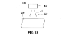
本発明による赤外線センシングデバイスと、前記赤外線センシングデバイスに赤外線を含む光を照射する光源とを備え、
前記光源から測定試料に照射され、かつ前記測定試料を透過した赤外線が、前記赤外線センシングデバイスにより検出される、
赤外線透過率測定装置、を提供する。
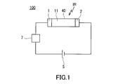
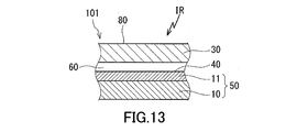
図1に示す赤外線センシングデバイス100は、抵抗可変部11と、抵抗可変部11に電圧を印加する第一電極1及び第二電極2とを備えている。電極1及び2には電源5から電圧が供給される。電源5は例えば直流電源である。抵抗可変部11と電極1及び2と電源5とを含む電気回路には測定部7が設けられている。図示は省略するが、デバイス100は、スイッチング素子その他の電子部品、測定結果を記憶するメモリ部、測定結果を表示する表示部、各部分及び部品の制御を担う制御部等を含んでいてもよい。この形態において、抵抗可変部11における電気抵抗の変化は、電極1及び2と測定部7とを用いて検出される。言い換えると、電気抵抗の変化を検出する検出部は、電極1及び2からなる電極群と、測定部7とを備えている。
LSPR-IR吸収材料におけるLSPRの存在は、例えば、周囲の媒質の屈折率を変化させた際の吸収ピークの波長変化に直線性があることを明らかにする方法により、確認することができる。LSPR-IR吸収材料は半導体であってもよい。
・ピコ秒レーザ(EKSPLA社製「PL2210A」、繰り返し周波数1kHz、パルス幅25ps、パルスエネルギー0.9mJ(波長1064nm))
・スーパーコンティニューム光源(Fianium社製「SC450」、繰り返し周波数20MHz、パルス幅50~100ps)
ただし、この条件は一例であり、局所表面プラズモン励起からの緩和時間の測定には、対象とする材料に応じた適切な条件を設定することができる。
酢酸銅1.891g、1,3-ジブチル-2-チオ尿素1.13g、オレイルアミン10mlを三又フラスコに投入し、攪拌しながら窒素置換を実施した。次いで、マントルヒーターを用い、液温を80℃に上昇させ、1時間保持した。その後、液温が40℃に低下した段階で、三又フラスコに40mlのクロロホルムを徐々に加えながら固形分を溶解させた。
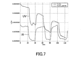
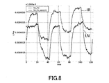
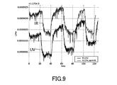
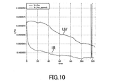
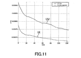
第2インクに含まれる第2化合物をアミノベンゾニトリルから表1に示した化合物に変更した以外は実施例1と同様にして、抵抗可変膜を形成した。また、抵抗可変膜について赤外光(IR)又は紫外光(UV)を照射しながら電流値の変化を測定した。結果を図6~10に示す。
(1)実施例1で用いた櫛形電極を形成したガラス板の上に、スピンコータを用いて50μlの硫化カドミウムナノ粒子インクを塗布し、塗布膜を得た。なお、塗布する際には、硫化カドミウムナノ粒子インクの濃度をオクタンで50mg/mlに調整した。
(2)塗布膜の上に、スピンコータを用いて1,2-エタンジチオール(EDT、バインダー)を含む200μlの溶液を塗布し、硫化カドミウムナノ粒子薄膜を得た。この溶液の溶媒はアセトニトリルであり、EDTの濃度は質量基準で0.03%とした。
(3)そして、(1)と(2)の操作を繰り返すことで抵抗可変膜として厚み110nmの硫化カドミウムナノ粒子膜(抵抗可変膜)を形成した。
(4) 硫化カドミウムナノ粒子膜の上に、スピンコータを用いて50μlの硫化銅ナノ粒子インクを塗布し、塗布膜を得た。なお、塗布する際には、硫化銅ナノ粒子インクの濃度を100mg/mlに調整した。
(5)(4)で得た塗布膜の上に、スピンコータを用いて1,2-エタンジチオール(EDT)を含む200μlの溶液を塗布し、硫化銅ナノ粒子薄膜を得た。この溶液の溶媒はアセトニトリルであり、EDTの濃度は質量基準で0.03%とした。
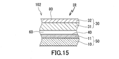
(6)そして、(4)(5)を繰り返すことで抵抗可変膜の上にキャリア供給部(キャリア供給膜)として厚み30nmの硫化銅ナノ粒子膜を形成した。なお、硫化カドミウムナノ粒子は一般的にn型、硫化銅ナノ粒子は一般的にp型の半導体材料である。
Claims (19)
- 赤外線センシングデバイスであって、
前記赤外線センシングデバイスへの赤外線の照射を受けて電気抵抗が変化する抵抗可変部と、前記抵抗可変部の電気抵抗の変化を検出する検出部とを備え、
前記抵抗可変部は、
i)局所表面プラズモン共鳴により赤外線を吸収しうる材料を含む、並びに、
ii)前記材料を含むとともに前記抵抗可変部に接するキャリア供給部への赤外線の照射により生じた電子及び/又は正孔であるキャリアを前記キャリア供給部から受け取る、からなる群より選ばれる少なくとも1つを満たす、
赤外線センシングデバイス。 - 前記検出部は、前記抵抗可変部に電圧を印加する電極群を含み、
前記電極群は、電源の正極に電気的に接続される第一電極と、電源の負極に電気的に接続される第二電極とを含み、
前記第一電極及び前記第二電極がともに、前記抵抗可変部及び/又は前記キャリア供給部に直接接している、請求項1に記載のデバイス。 - 前記検出部は、前記抵抗可変部に電圧を印加する電極群を含み、
前記電極群から前記抵抗可変部に電圧を印加しながら、前記抵抗可変部に赤外線の照射を開始し、その後前記照射を停止したときに、
前記照射の開始に応じて前記電気抵抗が増加し、前記照射の停止に応じて前記電気抵抗が減少する、請求項1に記載のデバイス。 - 前記抵抗可変部は、前記材料を含むとともに単層膜である、赤外線吸収膜を含む、請求項3に記載のデバイス。
- 前記抵抗可変部は、前記材料として、銅と、酸素を除くカルコゲン元素とを含む化合物を含む、請求項3又は4に記載のデバイス。
- 前記抵抗可変部は、前記材料として、硫化銅のナノ粒子を含む、請求項5に記載のデバイス。
- 前記検出部は、前記抵抗可変部に電圧を印加する電極群を含み、
前記電極から前記抵抗可変部に電圧を印加しながら、前記抵抗可変部に赤外線の照射を開始し、その後前記照射を停止したときに、
前記照射の開始に応じて前記電気抵抗が減少し、前記照射の停止に応じて前記電気抵抗が増加する、請求項1に記載のデバイス。 - 前記キャリア供給部を備え、
前記キャリア供給部と前記抵抗可変部とは積層構造を構成している、請求項7に記載のデバイス。 - 前記キャリア供給部と前記抵抗可変部とは、互いに異なる半導体材料から構成されている、請求項8に記載のデバイス。
- 前記抵抗可変部は、前記材料として、セシウムドープ酸化タングステンのナノ粒子を含む、請求項7~9のいずれか1項に記載のデバイス。
- 前記局所表面プラズモン共鳴により赤外線を吸収しうる材料は、局所表面プラズモン励起からの活性キャリアの緩和時間として1ns以上が測定されうる材料である、請求項1~10のいずれか1項に記載のデバイス。
- 前記抵抗可変部は、局所表面プラズモン共鳴により赤外線を吸収しうる材料である第1材料とともに、前記第1材料への赤外線の照射により生じた電子及び/又は正孔であるキャリアを受け取る第2材料を含む、請求項1~11のいずれか1項に記載のデバイス。
- 前記第1材料及び前記第2材料がともに透明導電性酸化物である、請求項12に記載のデバイス。
- 前記抵抗可変部は導電性炭素材料を含まない、請求項1~13のいずれか1項に記載のデバイス。
- 前記抵抗可変部の熱を外部に放出する放熱部をさらに備える、請求項1~14のいずれか1項に記載のデバイス。
- 前記赤外線センシングデバイスに照射される前記赤外線の少なくとも一部を透過させるカバー部をさらに備える、請求項1~15のいずれか1項に記載のデバイス。
- 前記カバー部は、基材と、前記基材に支持された、光学フィルタ部及び試料配置部からなる群より選択される少なくとも1つとを含む、請求項16に記載のデバイス。
- 請求項1~17のいずれか1項に記載の赤外線センシングデバイスと、前記赤外線センシングデバイスに赤外線を含む光を照射する光源とを備え、
前記光源から測定試料に照射され、かつ前記測定試料を透過した赤外線が、前記赤外線センシングデバイスにより検出される、赤外線透過率測定装置。 - 局所表面プラズモン共鳴により赤外線を吸収しうる材料を含み、
電圧を印加しながら、赤外線の照射を開始し、その後前記照射を停止したときに、
前記照射の開始に応じて電気抵抗が増加し、前記照射の停止に応じて前記電気抵抗が減少する、又は、
前記照射の開始に応じて電気抵抗が減少し、前記照射の停止に応じて前記電気抵抗が増加する、
赤外線センシングデバイス用の抵抗可変膜。
Priority Applications (4)
| Application Number | Priority Date | Filing Date | Title |
|---|---|---|---|
| US17/996,046 US12276550B2 (en) | 2020-04-13 | 2021-04-13 | Infrared sensing device and variable resistance film included in the same |
| JP2022515403A JP7837020B2 (ja) | 2020-04-13 | 2021-04-13 | 赤外線センシングデバイス及びそれに用いる抵抗可変膜 |
| CN202180027792.XA CN116075700A (zh) | 2020-04-13 | 2021-04-13 | 红外线传感器件和用于该器件的电阻可变膜 |
| EP21788628.2A EP4137789A4 (en) | 2020-04-13 | 2021-04-13 | INFRARED DETECTION DEVICE AND VARIABLE RESISTANCE FILM USING SAME |
Applications Claiming Priority (2)
| Application Number | Priority Date | Filing Date | Title |
|---|---|---|---|
| JP2020-071711 | 2020-04-13 | ||
| JP2020071711 | 2020-04-13 |
Publications (1)
| Publication Number | Publication Date |
|---|---|
| WO2021210593A1 true WO2021210593A1 (ja) | 2021-10-21 |
Family
ID=78085187
Family Applications (1)
| Application Number | Title | Priority Date | Filing Date |
|---|---|---|---|
| PCT/JP2021/015365 Ceased WO2021210593A1 (ja) | 2020-04-13 | 2021-04-13 | 赤外線センシングデバイス及びそれに用いる抵抗可変膜 |
Country Status (5)
| Country | Link |
|---|---|
| US (1) | US12276550B2 (ja) |
| EP (1) | EP4137789A4 (ja) |
| JP (1) | JP7837020B2 (ja) |
| CN (1) | CN116075700A (ja) |
| WO (1) | WO2021210593A1 (ja) |
Families Citing this family (1)
| Publication number | Priority date | Publication date | Assignee | Title |
|---|---|---|---|---|
| CN119805828B (zh) * | 2025-03-17 | 2025-07-15 | 中国人民解放军国防科技大学 | 一种光电耦合型lspr变红外发射率器件及其制备方法与应用 |
Citations (8)
| Publication number | Priority date | Publication date | Assignee | Title |
|---|---|---|---|---|
| JPH1062239A (ja) * | 1996-08-21 | 1998-03-06 | Mitsubishi Materials Corp | 赤外線検出素子 |
| JP2001013010A (ja) | 1999-06-28 | 2001-01-19 | Toyota Central Res & Dev Lab Inc | 抵抗変化型赤外線検出器 |
| JP2001183230A (ja) * | 1999-12-24 | 2001-07-06 | Kokusai Kiban Zairyo Kenkyusho:Kk | 光放射エネルギー強度測定装置 |
| JP2008139072A (ja) * | 2006-11-30 | 2008-06-19 | Nec Corp | 赤外線検知器及びその温度制御方法 |
| WO2016067905A1 (ja) * | 2014-10-30 | 2016-05-06 | 住友金属鉱山株式会社 | 熱線遮蔽粒子、熱線遮蔽粒子分散液、熱線遮蔽粒子分散体、熱線遮蔽粒子分散体合わせ透明基材、赤外線吸収透明基材、熱線遮蔽粒子の製造方法 |
| WO2018101446A1 (ja) * | 2016-12-02 | 2018-06-07 | 国立大学法人京都大学 | 光電変換機能を有する電子デバイス |
| JP2018524820A (ja) * | 2015-07-28 | 2018-08-30 | ネクスドット | 向上した性能を備える、ナノ結晶を利用した中遠赤外光検出器 |
| JP2019002852A (ja) * | 2017-06-16 | 2019-01-10 | 株式会社豊田中央研究所 | 電磁波検出器およびその製造方法 |
Family Cites Families (12)
| Publication number | Priority date | Publication date | Assignee | Title |
|---|---|---|---|---|
| JP2773730B2 (ja) * | 1996-03-07 | 1998-07-09 | 日本電気株式会社 | 光伝導型赤外線検出素子 |
| JP4441578B2 (ja) * | 2006-10-11 | 2010-03-31 | パナソニック株式会社 | 電子デバイスおよびその制御方法 |
| JP2009175124A (ja) * | 2007-12-27 | 2009-08-06 | Rohm Co Ltd | プラズモン共鳴検出器 |
| JP2012164980A (ja) * | 2011-01-21 | 2012-08-30 | Sumitomo Metal Mining Co Ltd | 光電変換装置とその製造方法 |
| EP2581721B1 (en) * | 2011-10-10 | 2019-05-08 | Samsung Electronics Co., Ltd | Infrared thermal detector and method of manufacturing the same |
| KR101922119B1 (ko) * | 2011-12-22 | 2019-02-14 | 삼성전자주식회사 | 적외선 검출기 및 이를 사용하는 적외선 검출 방법 |
| KR102040149B1 (ko) * | 2013-02-01 | 2019-11-04 | 삼성전자주식회사 | 적외선 검출기 |
| JP6172522B2 (ja) * | 2013-12-04 | 2017-08-02 | ソニー株式会社 | 赤外線検出素子およびその検出方法、並びに電子機器 |
| CN108884375B (zh) * | 2016-04-01 | 2021-05-11 | 住友金属矿山株式会社 | 红外线吸收材料、红外线吸收材料分散液、红外线吸收材料分散体、红外线吸收材料分散体夹层透明基材、红外线吸收透明基材 |
| CN110770555A (zh) | 2017-04-20 | 2020-02-07 | 特里纳米克斯股份有限公司 | 光学检测器 |
| JP7232978B2 (ja) * | 2017-12-11 | 2023-03-06 | パナソニックIpマネジメント株式会社 | 赤外線センサおよび赤外線センサのボロメータ赤外線受光部を冷却する方法 |
| TWI679782B (zh) * | 2017-12-19 | 2019-12-11 | 財團法人工業技術研究院 | 感測裝置及其製造方法 |
-
2021
- 2021-04-13 WO PCT/JP2021/015365 patent/WO2021210593A1/ja not_active Ceased
- 2021-04-13 CN CN202180027792.XA patent/CN116075700A/zh active Pending
- 2021-04-13 EP EP21788628.2A patent/EP4137789A4/en active Pending
- 2021-04-13 JP JP2022515403A patent/JP7837020B2/ja active Active
- 2021-04-13 US US17/996,046 patent/US12276550B2/en active Active
Patent Citations (8)
| Publication number | Priority date | Publication date | Assignee | Title |
|---|---|---|---|---|
| JPH1062239A (ja) * | 1996-08-21 | 1998-03-06 | Mitsubishi Materials Corp | 赤外線検出素子 |
| JP2001013010A (ja) | 1999-06-28 | 2001-01-19 | Toyota Central Res & Dev Lab Inc | 抵抗変化型赤外線検出器 |
| JP2001183230A (ja) * | 1999-12-24 | 2001-07-06 | Kokusai Kiban Zairyo Kenkyusho:Kk | 光放射エネルギー強度測定装置 |
| JP2008139072A (ja) * | 2006-11-30 | 2008-06-19 | Nec Corp | 赤外線検知器及びその温度制御方法 |
| WO2016067905A1 (ja) * | 2014-10-30 | 2016-05-06 | 住友金属鉱山株式会社 | 熱線遮蔽粒子、熱線遮蔽粒子分散液、熱線遮蔽粒子分散体、熱線遮蔽粒子分散体合わせ透明基材、赤外線吸収透明基材、熱線遮蔽粒子の製造方法 |
| JP2018524820A (ja) * | 2015-07-28 | 2018-08-30 | ネクスドット | 向上した性能を備える、ナノ結晶を利用した中遠赤外光検出器 |
| WO2018101446A1 (ja) * | 2016-12-02 | 2018-06-07 | 国立大学法人京都大学 | 光電変換機能を有する電子デバイス |
| JP2019002852A (ja) * | 2017-06-16 | 2019-01-10 | 株式会社豊田中央研究所 | 電磁波検出器およびその製造方法 |
Non-Patent Citations (1)
| Title |
|---|
| See also references of EP4137789A4 |
Also Published As
| Publication number | Publication date |
|---|---|
| EP4137789A4 (en) | 2023-10-11 |
| EP4137789A1 (en) | 2023-02-22 |
| US20230184592A1 (en) | 2023-06-15 |
| US12276550B2 (en) | 2025-04-15 |
| JP7837020B2 (ja) | 2026-03-30 |
| CN116075700A (zh) | 2023-05-05 |
| JPWO2021210593A1 (ja) | 2021-10-21 |
Similar Documents
| Publication | Publication Date | Title |
|---|---|---|
| Tang et al. | Enabling low-drift flexible perovskite photodetectors by electrical modulation for wearable health monitoring and weak light imaging | |
| Samouco et al. | Laser-induced electrodes towards low-cost flexible UV ZnO sensors | |
| Gogurla et al. | Multifunctional Au-ZnO plasmonic nanostructures for enhanced UV photodetector and room temperature NO sensing devices | |
| Rohizat et al. | Plasmon-enhanced reduced graphene oxide photodetector with monometallic of Au and Ag nanoparticles at VIS–NIR region | |
| Sturaro et al. | Degenerately doped metal oxide nanocrystals as plasmonic and chemoresistive gas sensors | |
| Gimenez et al. | ZnO− paper based photoconductive UV sensor | |
| Zhang et al. | Ultrasensitive photodetectors exploiting electrostatic trapping and percolation transport | |
| Cook et al. | Heat-assisted inkjet printing of tungsten oxide for high-performance ultraviolet photodetectors | |
| Xu et al. | Solution‐processed transparent self‐powered p‐CuS‐ZnS/n‐ZnO UV photodiode | |
| Yalagala et al. | ZnO nanowires based degradable high-performance photodetectors for eco-friendly green electronics | |
| Shi et al. | Split-ring structured all-inorganic perovskite photodetector arrays for masterly internet of things | |
| Bianchi et al. | Near infrared photothermoelectric effect in transparent AZO/ITO/Ag/ITO thin films | |
| Deng et al. | NIR-UV dual-mode photodetector with the assistance of machine-learning fabricated by hybrid laser processing | |
| Yuan et al. | High photosensitivity and low dark current of photoconductive semiconductor switch based on ZnO single nanobelt | |
| Xu et al. | Surface energy‐assisted patterning of vapor deposited all‐inorganic perovskite arrays for wearable optoelectronics | |
| Saimon et al. | Ag@ WO3 core–shell nanocomposite for wide range photo detection | |
| Shah et al. | Role of solvents in the preparation of methylammonium bismuth iodide (MBI) perovskite films for self-biased photodetector applications | |
| Mahana et al. | Photo-sensing characteristics of CuO thin films synthesized by thermal oxidation of Cu metal films | |
| WO2021210593A1 (ja) | 赤外線センシングデバイス及びそれに用いる抵抗可変膜 | |
| Tarwal et al. | Spray deposition of the nanostructured ZnO thin films for non-volatile resistive switching memory applications | |
| Sharma et al. | Quantum enhanced efficiency and spectral performance of paper-based flexible photodetectors functionalized with two dimensional materials | |
| US20230361235A1 (en) | Heat blocking device, heat blocking film, and heat blocking composition | |
| Wu et al. | A Self-Powered p-CuO/n-Si Heterojunction-Type Ultraviolet Photodetector | |
| Villegas et al. | UV-response of aluminum-doped zinc oxide transparent films with different microstructures and electrical properties | |
| Sharmila et al. | Wafer scale WS2 based ultrafast photosensing and memory computing devices for neuromorphic computing |
Legal Events
| Date | Code | Title | Description |
|---|---|---|---|
| 121 | Ep: the epo has been informed by wipo that ep was designated in this application |
Ref document number: 21788628 Country of ref document: EP Kind code of ref document: A1 |
|
| ENP | Entry into the national phase |
Ref document number: 2022515403 Country of ref document: JP Kind code of ref document: A |
|
| NENP | Non-entry into the national phase |
Ref country code: DE |
|
| ENP | Entry into the national phase |
Ref document number: 2021788628 Country of ref document: EP Effective date: 20221114 |
|
| WWG | Wipo information: grant in national office |
Ref document number: 17996046 Country of ref document: US |