WO2021240965A1 - 光走査装置 - Google Patents
光走査装置 Download PDFInfo
- Publication number
- WO2021240965A1 WO2021240965A1 PCT/JP2021/011400 JP2021011400W WO2021240965A1 WO 2021240965 A1 WO2021240965 A1 WO 2021240965A1 JP 2021011400 W JP2021011400 W JP 2021011400W WO 2021240965 A1 WO2021240965 A1 WO 2021240965A1
- Authority
- WO
- WIPO (PCT)
- Prior art keywords
- piezoelectric
- drive
- axis
- optical scanning
- output voltage
- Prior art date
- Legal status (The legal status is an assumption and is not a legal conclusion. Google has not performed a legal analysis and makes no representation as to the accuracy of the status listed.)
- Ceased
Links
Images






Classifications
-
- G—PHYSICS
- G02—OPTICS
- G02B—OPTICAL ELEMENTS, SYSTEMS OR APPARATUS
- G02B26/00—Optical devices or arrangements for the control of light using movable or deformable optical elements
- G02B26/08—Optical devices or arrangements for the control of light using movable or deformable optical elements for controlling the direction of light
- G02B26/10—Scanning systems
- G02B26/101—Scanning systems with both horizontal and vertical deflecting means, e.g. raster or XY scanners
-
- G—PHYSICS
- G02—OPTICS
- G02B—OPTICAL ELEMENTS, SYSTEMS OR APPARATUS
- G02B26/00—Optical devices or arrangements for the control of light using movable or deformable optical elements
- G02B26/08—Optical devices or arrangements for the control of light using movable or deformable optical elements for controlling the direction of light
- G02B26/0816—Optical devices or arrangements for the control of light using movable or deformable optical elements for controlling the direction of light by means of one or more reflecting elements
- G02B26/0833—Optical devices or arrangements for the control of light using movable or deformable optical elements for controlling the direction of light by means of one or more reflecting elements the reflecting element being a micromechanical device, e.g. a MEMS mirror, DMD
- G02B26/0858—Optical devices or arrangements for the control of light using movable or deformable optical elements for controlling the direction of light by means of one or more reflecting elements the reflecting element being a micromechanical device, e.g. a MEMS mirror, DMD the reflecting means being moved or deformed by piezoelectric means
-
- H—ELECTRICITY
- H02—GENERATION; CONVERSION OR DISTRIBUTION OF ELECTRIC POWER
- H02N—ELECTRIC MACHINES NOT OTHERWISE PROVIDED FOR
- H02N2/00—Electric machines in general using piezoelectric effect, electrostriction or magnetostriction
- H02N2/10—Electric machines in general using piezoelectric effect, electrostriction or magnetostriction producing rotary motion, e.g. rotary motors
- H02N2/14—Drive circuits; Control arrangements or methods
Definitions
- the present invention relates to an optical scanning device including an optical deflector.
- a light beam from a light source is irradiated to a mirror unit that reciprocates around an axis, and the scanning light beam is emitted from the mirror unit. ing.
- MEMS Micro Electro Mechanical Systems
- Patent Document 1 discloses a MEMS uniaxial scanning type optical deflector.
- cantilever levers are coupled from both sides to a torsion bar protruding from the mirror portion along the axis of rotation.
- Each cantilever is divided into two piezoelectric compartments, a piezoelectric compartment that acts as a piezoelectric actuator in the longitudinal direction and a piezoelectric compartment that acts as a piezoelectric sensor for detecting runout angle.
- Patent Document 2 discloses a MEMS 2-axis scanning type optical deflector.
- each pair of semi-annular piezoelectric actuators is arranged on each side of the rotation axis, coupled from each side at the same position in the longitudinal direction of the torsion bar, and surrounds the mirror portion in an annular shape.
- Each semi-annular piezoelectric actuator consists of one piezoelectric actuator, and the semi-annular piezoelectric actuators on each side are driven by drive voltages of opposite phases to each other and reciprocate around the mirror portion around the rotation axis via the torsion bar. Rotate.
- Patent Document 3 discloses a MEMS uniaxial scanning type optical deflector.
- an annular piezoelectric body surrounds the mirror portion and is coupled to the intermediate portion of each torsion bar protruding from the mirror portion along the rotation axis on the rotation axis of the mirror portion.
- the annular piezoelectric body has three piezoelectric compartments, a central piezoelectric compartment and a piezoelectric compartment at both ends, in a half portion on each side of the axis of rotation.
- Each central piezoelectric partition portion is driven by a drive voltage of opposite phase, and the mirror portion is reciprocated around a rotation axis via a torsion bar.
- the outputs of the piezoelectric compartments at both ends on the same side of the rotating shaft are added as a piezoelectric sensor, and the deflection angle of the mirror portion around the rotating shaft is detected based on the added output.
- An object of the present invention is to obtain a sufficient output voltage even when the runout angle of the mirror portion around the rotation axis is small without adding a special piezoelectric sensor, and to detect the runout angle with high accuracy. It is to provide a scanning device.
- the optical scanning device of the present invention is Piezoelectricity having a mirror portion, a support portion, and a plurality of piezoelectric partition portions coupled in series, interposed between the support portion and the mirror portion, and reciprocating the mirror portion around a rotation axis.
- an optical deflector including an actuator
- the plurality of piezoelectric compartments are arranged alternately from the base end side to the working end side of the optical deflector into the first set and the second set, the first set and the second set of piezoelectric sections are grouped.
- a drive unit that supplies the first drive voltage and the second drive voltage in phases that are in opposite phase to each other, respectively.
- a detection unit that detects the deflection angle of the mirror unit around the rotation axis, and a detection unit.
- a drive voltage is supplied to the piezoelectric partition portions of both the first set and the second set.
- the drive voltage is supplied only to the piezoelectric partition portion of one of the first set and the second set.
- the detection unit detects the runout angle based on the output voltage of the other set of piezoelectric compartments.
- the drive voltage is supplied and operated only to the first set of piezoelectric compartments, while the second set of piezoelectric compartments is operated. Used as a piezoelectric sensor. As a result, a sufficient output voltage can be obtained even when the runout angle of the mirror portion around the rotation axis is small without adding a special piezoelectric sensor, and the runout angle can be detected with high accuracy.
- the support portion surrounds the mirror portion in an annular shape.
- the optical deflector has a pair of torsion bars extending from both sides of the mirror portion and coupled to the support portion.
- the piezoelectric actuator encloses the mirror portion in an annular shape on the inner peripheral side of the support portion, and is coupled to the intermediate portion of the pair of torsion bars on the axis of the first axis as the rotation axis, and the mirror portion. It is an annular piezoelectric actuator coupled to the support portion on the second axis orthogonal to the first axis at the center of the.
- each torsion bar is given rotational power from both sides with respect to the first axis. This makes it possible to stabilize the reciprocating rotation during the low runout angle period.
- the optical scanning apparatus of the present invention is Further, a pair of piezoelectric sensors arranged with the first axis sandwiched from both sides at at least one coupling portion of the coupling portion of the annular piezoelectric actuator coupled to the pair of torsion bars is provided.
- the detection unit detects the runout angle based on the output voltage of the pair of piezoelectric sensors during the first drive period.
- both the drive voltages of the first set and the second set are used to secure a large swing angle width of the mirror portion, and sufficient from the pair of piezoelectric sensors.
- the runout angle can be detected by the output voltage.
- the detection unit detects the runout angle based on the addition of the output voltage of the piezoelectric section portion of the other set and the output voltage of the pair of the pair of piezoelectric sensors. ..
- the runout angle is detected based on the addition of the output voltage of the other set of piezoelectric compartments and the output voltage of the pair of piezoelectric sensors, so that the runout angle is detected in the second drive period.
- the output voltage on which angle detection is based can be further increased.
- the optical scanning apparatus of the present invention is Further, during the second drive period, a connection switching unit for connecting at least one output terminal of the pair of piezoelectric sensors to the ground is provided.
- the output terminal of the piezoelectric sensor is connected to the ground during the second drive period. This makes it possible to prevent the charge from accumulating in the unused piezoelectric sensor during the second drive period.
- connection switching unit alternately switches the other set between the first set and the second set during the second drive period.
- FIG. 1 is a schematic diagram of the entire optical scanning device 10.
- the optical scanning device 10 includes a laser light source 20, an optical deflector 30, and a control unit 45.
- the screen 90 is shown in FIG. 1, the screen 90 is excluded from the elements constituting the optical scanning device 10.
- the screen 90 is only shown for convenience of explaining the scanning locus Cr by the scanning light beam Ls emitted from the optical scanning device 10.
- the screen 90 may be a video screen or an irradiation area in front of the vehicle, depending on the product such as a video device or a vehicle headlight in which the optical scanning device 10 is incorporated.
- the vertical and horizontal sides of the screen 90 correspond to the vertical (V) direction and the horizontal (H) direction, respectively.
- the element name and the element having V or H in the factor name mean that they are related to the vertical direction and the horizontal direction in each direction, respectively.
- the laser light source 20 emits a laser beam Lo toward the mirror portion 31 of the light deflector 30.
- the mirror unit 31 emits the scanning light beam Ls generated by reflecting the laser light beam Lo.
- the mirror unit 31 resonates and reciprocates around the two axes of the first axis and the second axis, which are orthogonal to each other, respectively.
- the H-axis and the V-axis correspond to the first axis and the second axis, respectively.
- the scanning light beam Ls generates a scanning locus Cr on the screen 90 by raster scanning.
- the control unit 45 includes a drive unit 49, a detection unit 50, a connection switching unit 51, and a light source control unit 52.
- the light source control unit 52 controls switching between turning on and off the laser light source 20 and the amount of energization (luminous intensity of the laser light beam Lo) when the laser light source 20 is turned on. Details of the drive unit 49, the detection unit 50, and the connection switching unit 51 will be described later.
- FIG. 2 is a front view of the light deflector 30.
- the X-axis and the Y-axis are axes parallel to the horizontal and vertical directions in the front view of the optical deflector 30.
- the Z axis is an axis parallel to the thickness direction of the MEMS optical deflector 30.
- the optical deflector 30 includes a mirror portion 31, a pair of torsion bars 32a and 32b, an H actuator, a movable frame 34, a pair of V actuators 35a and 35b, and a fixed frame 36.
- the mirror portion 31 is circular, and the laser beam Lo (FIG. 1) is incident on the center O of the mirror portion 31.
- the first and second axes as the two rotation axes of the mirror portion 31 of the optical deflector 30 which is a two-axis optical deflector are parallel to the Y-axis and the X-axis when the mirror portion 31 is stationary. And the relationship is orthogonal at the center O.
- the annular H actuator 33 and the annular movable frame 34 surround the mirror portion 31 in order from the inside.
- the torsion bars 32a and 32b extend along the first axis on both sides of the mirror portion 31, and are coupled to the peripheral edge of the mirror portion 31 and the inner circumference of the H actuator 33 at both ends, respectively.
- the annular H actuator 33 is coupled to the intermediate portion of the torsion bar 32 (general term for the torsion bar 32a and the torsion bar 32b).
- the H actuator 33 receives the supply of the H drive voltage (first drive voltage) and resonates the mirror portion 31 around the first axis at a resonance frequency (eg, 15 kHz) via the torsion bar 32.
- the H actuator 33 has a first set 39 and a second set 40 as a set of piezoelectric partition portions. Details of the first set 39 and the second set 40 will be described later in FIG.
- the V actuators 35a and 35b are located on both sides of the movable frame 34 in the X-axis direction.
- Each V-actuator 35 (general term for V-actuators 35a and 35b) is interposed between the outer circumference of the movable frame 34 and the inner circumference of the fixed frame 36.
- Each V-actuator 35 has a plurality of cantilever 37s coupled in parallel in the Y-axis direction and in series in a meander arrangement.
- a V drive voltage is supplied that has the same amplitude and frequency and is 180 ° out of phase (in a mutually opposite phase relationship).
- the frequency of the V drive voltage is set to a non-resonant frequency (example: 60 Hz), and is set to a value significantly lower than the resonance frequency of the reciprocating rotation of the mirror portion 31 around the first axis.
- the mirror portion 31 reciprocates around the second axis (non-resonant axis) in a non-resonant manner.
- the H actuator 33 and the V actuator 35 are both unipolar type piezoelectric actuators.
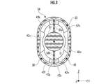
- FIG. 3 is a detailed view of the H actuator 33.
- the H actuator 33 is formed in an oval shape long in the Y-axis direction (eg, track shape of an athletics stadium), and has a symmetrical shape with the first axis parallel to the Y-axis as the axis of symmetry.
- the H actuator 33 is coupled to the intermediate portion of the torsion bar 32 at two points intersecting the first axis.
- the coupling portion functions as the working end of the H actuator 33.
- the H actuator 33 also intersects the second axis at two points and is coupled to the inner circumference of the movable frame 34 on the outer peripheral side of the intersection.
- the coupling portion functions as a base end of the H actuator 33.
- the optical deflector 30 stacks three layers on the surface of the SOI substrate in order from the bottom, on the lower electrode layer, the piezoelectric film layer, and the upper electrode layer by film formation. After that, for the region other than the piezoelectric actuator, these three layers are removed by etching to complete the optical deflector 30. By dicing one SOI substrate, a plurality of optical deflectors 30 are cut out.
- SOI is composed of five layers, in order from the bottom, an oxide film layer on the back surface, a Si layer for handling, an oxide film layer, an upper Si layer, and an oxide film layer on the front surface. Except for the H actuator 33 and the V actuator 35, the lower electrode layer, the piezoelectric film layer, and the upper electrode layer are removed by etching. Further, in the region of the H actuator 33 and the V actuator 35, the two layers on the back surface side of the SOI substrate are removed by etching from the back surface side, and the upper three layers constitute the substrate portion.
- the H actuator 33 has one proximal end on each side with respect to the first axis of the axis of symmetry.
- the H actuator 33 is of 42a, 42b, 42c, 42d, 42e, 42f (hereinafter, abbreviated as "piezoelectric partition portion 42a-piezoelectric partition portion 42f") in order from the base end on the V actuator 35a side in the clockwise direction. It has a total of 6 piezoelectric compartments.
- the arrangement of the total of 6 piezoelectric compartments 42a-piezoelectric compartments 42f is symmetrical with respect to the first axis, and as a result, the number of piezoelectric compartments on each side with respect to the first axis is the same. ..
- the plurality of piezoelectric partition portions are alternately grouped into a first set and a second set in the order of the circumferential direction.
- the piezoelectric section portions 42a, 42c, 42e form the first set 39 with these three sections
- the piezoelectric section portions 42b, 42d, 42f form the second set 40 with these three sections. As shown in FIG.
- the first set and the second set have the same total area, and the arrangement balance of each piezoelectric section portion in each set is equal. Therefore, the mirror can be rotated evenly to the left and right in the horizontal direction only by driving one of the sets of piezoelectric compartments (3 compartments).
- the first set and the second set can be operated individually. Further, if the drive voltage supplied to the first set and the drive voltage supplied to the second set are made the same when individually operated, the rotation angle and rotation of the first mirror around the first axis are made the same. The frequencies will be the same.
- the drive unit 49 supplies the first drive voltage to the piezoelectric section portion of the first set 39, and supplies the second drive voltage to the piezoelectric section portion of the second set 40. Only the phase of the first drive voltage and the second drive voltage is opposite to each other, and the other frequencies, waveforms, and bias voltages are the same.
- Piezoelectric partition portion 42a-The piezoelectric partition portion 42f has a laminated structure in which the above-mentioned upper three layers of SOI are used as a substrate layer, and a lower electrode layer, a piezoelectric film layer, and an upper electrode layer are provided on the surface side thereof. It has become.
- a dividing groove that divides the upper electrode layer and the piezoelectric film layer is formed between the piezoelectric section portions that are adjacent to each other in the circumferential direction. As a result, a short circuit between the piezoelectric partition portions adjacent to each other in the circumferential direction is prevented.
- the piezoelectric sensors 43a and 43b are formed in the region of the H actuator 33 that sandwiches the intersection with the torsion bar 32b from both sides.
- the piezoelectric sensor 43 (general term for the piezoelectric sensors 43a and 43b) is located between the piezoelectric partition portion 42e and the piezoelectric partition portion 42f in the circumferential direction, and generates an output voltage different from that of the piezoelectric partition portion 42a-piezoelectric partition portion 42f. Let me. Further, the piezoelectric sensors 43a and 43b both have a smaller area than the piezoelectric compartment portion 42a-piezoelectric compartment portion 42f.
- the first set 39 and the second set 40 receive the first drive voltage and the second drive voltage having opposite phases to each other, respectively.
- the first set 39 and the second set 40 are curved and deformed in opposite phases, and the H actuator 33 reciprocates the mirror portion 31 around the first axis via the torsion bar 32. Since the H actuator 33 has both the first set 39 and the second set 40 on each side with respect to the first axis, it is possible to increase the swing angle width around the first axis.
- the piezoelectric sensors 43a and 43b are curved and deformed in the same phase as the set of piezoelectric compartments that are not adjacent to each other in the circumferential direction on the H actuator 33, and generate an output voltage according to the amount of deformation.
- the output voltage of the piezoelectric sensor 43 is sent to the detection unit 50.
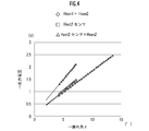
- FIG. 4 is a graph showing the relationship between the runout angle ⁇ of the mirror portion 31 around the first axis and each output voltage.
- the runout angle ⁇ 0 ° is defined as the runout angle when the mirror portion 31 faces directly in front of the optical deflector 30.
- the horizontal axis of FIG. 4 shows the deflection angle ⁇ on one side of the mirror portion 31 with respect to the direction directly in front of the optical deflector 30. Since the optical deflector 30 has a configuration symmetrical with respect to the first axis, the mirror portion 31 has the same relationship with respect to the deflection angle ⁇ on the other side with respect to the direction directly in front of the optical deflector 30. ..
- hact1 1st set 39
- hact2 2nd group 40
- hact1 sensor 1st set 39 diverted to a piezoelectric sensor
- hact2 sensor 2nd set 40 diverted to piezoelectric sensor
- hsen1 Piezoelectric sensor 43a
- hsen2 Piezoelectric sensor 43b SW (Fig. 6A, etc.): Switch
- the added value of the output voltages of the piezoelectric sensors 43a and 43b is low in a region where the runout angle ⁇ is low (as a guide, a region where the runout angle ⁇ ⁇ 5 ° with 5 ° as a threshold value). Therefore, the detection accuracy of the runout angle ⁇ is lowered.
- the output voltage of the second set 40 ( ⁇ : Hact2 sensor) is larger than the added value of the output voltages of the piezoelectric sensors 43a and 43b.
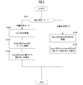
- FIG. 5 is a flowchart of a method for detecting a runout angle ⁇ in the optical scanning apparatus 10. Before explaining the flowchart, a specific circuit to which the detection method of the flowchart is applied will be described.
- the normal runout angle mode (high runout angle mode) is one, while the low runout angle mode is 1-3.
- the normal runout angle mode (high runout angle mode) is a runout angle mode used in the first drive period, and runout when the runout angle width of the mirror unit 31 exceeds the threshold value ⁇ a and the runout angle is controlled. It is a corner mode.
- the low runout angle mode is a runout angle mode used in the second drive period, and the runout angle when the runout angle is controlled with a small runout angle width in which the runout angle width of the mirror unit 31 is equal to or less than the threshold value ⁇ a. The mode.
- the relationship between the element (piezoelectric material) used as the (piezoelectric) sensor in each runout angle mode and the phase difference between the sensors (phase difference of the output voltage of the target element with respect to the phase of the output voltage of the reference element) is as follows. It is a street.
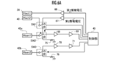
- FIG. 6A and 6B are phase diagrams of the first drive period and the second drive period in the external circuit in which the low runout angle mode is set to the low runout angle mode 1, respectively.
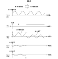
- FIG. 7 is a waveform diagram of the first drive period and the second drive period in the external circuit.
- the low runout angle mode 1 corresponds to the detection method of (b1).
- control unit 45 controls the connection position of SW (switch) 1-SW3.
- SW switch
- 66 and 67 are drive amplifiers.
- 68-71 are sensor amplifiers.
- 75 and 76 are resistors.
- the control unit 45 supplies the first drive voltage and the second drive voltage to the first set 39 and the second set 40 via the drive amplifiers 66 and 67, respectively.
- the output voltages of the second set 40 and the piezoelectric sensor 43a are sent to the control unit 45 via the sensor amplifiers 68 and 69.
- the output voltage of the piezoelectric sensor 43b is sent to the control unit 45 via the sensor amplifiers 70 and 71.
- SW1 connects the second set 40 to the contact A when the first drive period (FIG. 6A), that is, the second set 40 is used in the piezoelectric actuator, and the second drive period (FIG. 6B), that is, the second set 40. Is used in the piezoelectric sensor, the second set 40 is connected to the contact B.
- SW2 and SW3 are both contact positions of contact A and contact B during the first drive period and the second drive period, respectively.
- the binary level of SW1-SW3 "0" indicates that the connection position is at contact A, and "1" indicates that the connection position is at contact B.
- the first drive voltage and the second drive voltage are drive voltages having opposite phases to each other.
- the mirror portion 31 reciprocates around the first axis with a large swing angle width. That is, the scanning light beam Ls scans in the H direction with a large scanning width.
- the piezoelectric sensors 43a and 43b are curved and deformed in opposite phases to each other, and in the first drive period, they generate output voltages in opposite phases to each other.
- the control unit 45 (specifically, the detection unit 50 of the control unit 45) inverts the output voltage of the piezoelectric sensor 43b, then adds it to the output voltage of the piezoelectric sensor 43a, and adds the value after the addition (specifically, the detection unit 50 of the control unit 45).
- the runout angle ⁇ in the first drive period is detected based on (see “ ⁇ ” in FIG. 4). Since the runout angle width in the first drive period is sufficiently large, the detection accuracy of the runout angle ⁇ is sufficiently guaranteed.
- both SW1 and SW2 are at the connection position of the contact B.
- the H actuator 33 reciprocates the mirror portion 31 around the first axis only by the piezoelectric section portion of the first set 39. Therefore, the actuator force by the H actuator 33 is halved, but the second drive period is a period in which the mirror portion 31 is reciprocated around the first axis with a small deflection angle width, and the mirror portion 31 is the first. It reciprocates without any trouble with the specified deflection angle width around the shaft.
- the output voltage of the piezoelectric section portion of the second set 40 is sent to the control unit 45.
- the detection unit 50 of the control unit 45 detects the runout angle ⁇ based on the output voltage of the piezoelectric section portion of the second set 40. Since the output voltage of the piezoelectric section portion of the second set 40 is larger than the output voltage of the added value of the piezoelectric sensors 43a and 43b (see the comparison between “ ⁇ ” and “ ⁇ ” in FIG. 4), the detection unit 50 is sufficient.
- the runout angle ⁇ can be detected with high accuracy.
- the piezoelectric partition portions 42b, 42d, and 42f of the second set 40 are located at locations farther from the torsion bar 32b than the piezoelectric sensors 43a and 43b, too much stress is applied from the torsion bar to peel them off. Is prevented.
- the drive unit 49 determines the runout angle mode in which the mirror unit 31 is reciprocally rotated around the first axis. There are two runout angle modes, a low runout angle mode and a high runout angle mode. Specifically, when the drive unit 49 reciprocates the mirror unit 31 with the swing angle width of the swing angle ⁇ set to the threshold value ⁇ a or less, the drive unit 49 determines that the control period of the low swing angle mode is set, and determines that the swing angle ⁇ is the control period. When the runout angle width is made larger than the threshold value ⁇ a and reciprocated, it is determined that the control period is the high runout angle mode.
- the drive unit 49 determines that the control period is in the low runout angle mode, the drive unit 49 advances the process to S102.
- the drive unit 49 determines that the control period is in the high runout angle mode, the drive unit 49 advances the process to S108.
- the drive unit 49 stops the output of the second drive voltage, outputs only the first drive voltage, and drives only the piezoelectric section portion of the first set 39.
- the actuator force of the mirror unit 31 is halved, but the width of the deflection angle ⁇ required for the mirror unit 31 during this period is small, so that the mirror unit 31 reciprocates around the first axis. There is no problem with.
- connection switching unit 51 connects the piezoelectric sensors 43a and 43b to the ground. Specifically, as shown in FIG. 6B, the connection switching unit 51 switches all the connection positions of SW1-SW3 to the contact B. As a result, the output terminals of the piezoelectric sensors 43a and 43b are maintained at 0 V (earth), and depolarization due to charge accumulation during bending deformation is prevented.
- connection position of SW1 is switched from the contact A to the contact B
- the function of the second set 40 is switched from the piezoelectric actuator to the piezoelectric sensor.
- the detection unit 50 detects the runout angle ⁇ based on the output voltage Voa2 of the piezoelectric section portion of the second set 40. As described by “ ⁇ ” in FIG. 4, although the mirror unit 31 is in the low runout angle mode, the output voltage of the detection unit 50 is ensured to have a sufficient magnitude. Therefore, the detection accuracy of the runout angle ⁇ in the low runout angle mode is guaranteed.
- the drive unit 49 drives the first set 39 and the second set 40 with both the first output voltage and the second output voltage, respectively.
- the connection switching unit 51 switches all of SW1-SW3 to the contact A (FIG. 6B).
- the piezoelectric partition portions of both the first set 39 and the second set 40 are driven, so that the H actuator 33 outputs a large actuator force.
- the mirror portion 31 can reciprocate with a large swing angle width around the first axis.
- the detection unit 50 detects the runout angle ⁇ based on the added value of the output voltages Vos1 and Vos2 of the piezoelectric sensors 43a and 43b. As described by “ ⁇ ” in FIG. 4, the swing angle width of the swing angle ⁇ in the high swing angle mode is large. Therefore, the detection accuracy of the runout angle ⁇ in the high runout angle mode is guaranteed.
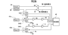
- FIG. 8A is a diagram showing a connection state during the second drive period in an external circuit in which the low runout angle mode is set to the low runout angle mode 2.
- the low runout angle mode 2 corresponds to the detection method of (b2).
- FIG. 8B is a waveform diagram of the second drive period in the external circuit of FIG. 8A. Since the connection position of the first drive period in the control unit 45 of FIG. 8A is the same as that of FIG. 6A, the illustration is omitted. Further, since the waveform diagram of the first set 39, SW1, SW2 and the piezoelectric sensor 43a in the first drive period in the control unit 45 of FIG. 8A is the same as the waveform diagram with those in FIG. 7, the illustration is omitted.
- FIGS. 8A and 8B the differences from FIGS. 6B and 7 will be described.
- SW3 becomes the connection position of the contact A.
- the detection unit 50 detects the runout angle ⁇ based on the added value of the output voltage of the piezoelectric section portion of the second set 40 and the output voltage of the piezoelectric sensor 43b.
- the output voltage of the piezoelectric sensor 43b has a phase opposite to the output voltage of the piezoelectric section portion of the second set 40. Therefore, the detection unit 50 inverts the output voltage of the piezoelectric sensor 43b and then adds it to the output voltage of the piezoelectric section portion of the second set 40.
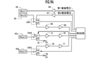
- FIG. 9A is a diagram showing a connection state in the second drive period in an external circuit in which the low runout angle mode is set to the low runout angle mode 3.
- the low runout angle mode 3 corresponds to the detection method of (b3).
- 9B is a waveform diagram of the external circuit of FIG. 9A. Since the connection position of the first drive period in the control unit 45 of FIG. 9A is the same as that of FIG. 6A, the illustration is omitted. Further, since the waveform diagrams of the first set 39, SW1, SW2 and the piezoelectric sensor 43a in the first drive period in the control unit 45 of FIG. 9B are the same as those waveform diagrams of FIG. 7, the illustration is omitted.
- FIGS. 9A and 9B the differences from FIGS. 6B and 7 will be described.
- a dedicated sensor amplifier 77, 78 is prepared separately from the sensor amplifiers 68, 69 for the piezoelectric partition portion of the second set 40.
- both SW2 and SW3 switch the connection position to the contact A.
- the detection unit 50 detects the runout angle ⁇ based on the added value of the output voltage of the piezoelectric section portion of the second set 40 and the added value of the output voltages of the piezoelectric sensors 43a and 43b.
- FIG. 10 is a circuit diagram of a drive system that alternately switches between a drive group and a non-drive group during the second drive period.
- the driven group and the non-driven group in the second drive period are hereinafter referred to as a first operation period in which the first set 39 and the second set 40 are used, respectively, and a second operation period in which the second set 40 and the first set 39 are used.
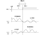
- FIG. 11 is a diagram showing the waveforms of each operating period in comparison with each other in the circuit of FIG.
- connection positions of SW6 and SW7 are switched by a control signal from the control unit 45.
- FIG. 10 and the left half of FIG. 11 show the connection position and waveform of the first operation period
- the lower figure of FIG. 10 and the right half of FIG. 11 show the connection position of the second operation period. And the waveform are shown.
- the first operation period and the second operation period are alternately switched, for example, at regular time intervals in the second drive period.
- the connection positions of SW6 and SW7 are both contacts A.
- the first drive voltage is supplied to the first set 39, while the supply of the second drive voltage to the second set 40 is stopped.
- the piezoelectric section portion of the first set 39 operates as the piezoelectric section, while the piezoelectric section portion of the second set 40 outputs the output voltage related to the runout angle ⁇ as the piezoelectric sensor.
- the output voltage from the piezoelectric sensors 43a and 43b is input to the detection unit 50 together with the output voltage from the second set 40, and the detection unit 50 uses the output voltage from these three elements (piezoelectric bodies) as the output voltage.
- the runout angle ⁇ is detected based on this.
- the connection positions of SW6 and SW7 are both switched to contact B.
- the supply of the first drive voltage from the drive unit 49 to the first set 39 is stopped, while the supply of the second drive voltage from the drive unit 49 to the second set 40 is carried out.
- the piezoelectric section portion of the second set 40 operates as the piezoelectric actuator, while the first set 39 outputs the output voltage related to the runout angle ⁇ as the piezoelectric sensor.
- the output voltage from the piezoelectric sensors 43a and 43b is input to the detection unit 50 together with the output voltage from the first set 39, and the detection unit 50 uses the output voltage from these three elements (piezoelectric bodies) as the output voltage.
- the runout angle ⁇ is detected based on this.
- the driven group and the non-driven group are alternately switched between the first group 39 and the second group 40 in the second drive period, so that each piezoelectric partition portion alternately repeats the operation and stop of the piezoelectric actuator. Therefore, the life is improved.
- piezoelectric sensors are provided on both sides of the first axis at at least one of the two coupling portions where the H actuator 33 couples with the torsion bar 32 (eg, the coupling portion on the torsion bar 32b side). Forty-three pairs are provided.
- the optical deflector 30 of the embodiment is a two-axis optical deflector.
- the optical deflector provided in the optical scanning device of the present invention may be a uniaxial optical deflector.
- the H actuator 33 of the embodiment is formed in an annular shape.
- the piezoelectric actuator provided in the optical scanning apparatus of the present invention may be a linear (non-annular) piezoelectric actuator coupled to both sides of each torsion bar as in Patent Document 1.
- Hact2 sensor + Hsen2 only one of the Hact2 sensor + Hsen2 is used as the combination of the output voltages used as the basis for detecting the runout angle ⁇ .
- Other combinations of the present invention include (c1) Hact2 sensor + Hsen1, (c2) Hact2 sensor + Hsen1 + Hsen2, (c3) Hact2 sensor + Hsen2, (c4) Hact1 sensor + Hsen1, and (c5) Hact1 sensor + Hsen1 + Hsen2. May be.
- the movable frame 34 as the support portion has an annular shape surrounding the mirror portion 31.
- the support portion does not have to be an annular shape that surrounds the mirror portion from the outside.
- the support portion of the present invention may have a structure that supports the mirror portion from one side.
- Optical scanning device 20 ... Laser light source, 30 ... Optical deflector, 31 ... Mirror unit, 32a, 32b ... Torsion bar, 33 ... H actuator (annular piezoelectric actuator) , 34 ... Movable frame (support part), 39 ... 1st set, 40 ... 2nd set, 42a-42f ... Piezoelectric section, 43a, 43b ... Piezoelectric sensor, 45 ... Control unit, 49 ... Drive unit, 50 ... Detection unit, 51 ... Connection switching unit.
Landscapes
- Physics & Mathematics (AREA)
- General Physics & Mathematics (AREA)
- Optics & Photonics (AREA)
- Mechanical Optical Scanning Systems (AREA)
- General Electrical Machinery Utilizing Piezoelectricity, Electrostriction Or Magnetostriction (AREA)
- Mechanical Light Control Or Optical Switches (AREA)
- Micromachines (AREA)
Abstract
本発明の光走査装置は、光偏向器と、駆動部と、検出部とを備える。光偏向器は、ミラー部(31)及びHアクチュエータ(33)を有する。駆動部は、Hアクチュエータ(33)の第1組の圧電区画部分(42a,42c,42e)及び第2組の圧電区画部分(42b,42d,42f)に対し、第1駆動期間では第1駆動電圧及び第2駆動電圧の両方を供給し、第2駆動期間では、第1組及び第2組の一方の組の圧電区画部分にのみ駆動電圧を供給する。検出部は、第2駆動期間には、他方の組の圧電区画部分の出力電圧に基づいて振れ角γを検出する。
Description
本発明は、光偏向器を備える光走査装置に関する。
MEMS(Micro Electro Mechanical Systems)の光偏向器を装備する光走査装置では、光源からの光ビームを、軸の回りに往復回動するミラー部に照射させて、走査光ビームをミラー部から出射させている。ミラー部からの走査光ビームの出射方向が正確に制御されるためには、軸の回りのミラー部の振れ角を正確に検出する必要がある。
特許文献1は、MEMSの1軸走査方式の光偏向器を開示する。この光偏向器では、ミラー部から回転軸に沿って突出するトーションバーに両側からカンチレバーを結合している。各カンチレバーは、長手方向に圧電アクチュエータとして作用する圧電区画部分と、振れ角検出用の圧電センサとして作用する圧電区画部分との2つの圧電区画部分に区分される。
特許文献2は、MEMSの2軸走査方式の光偏向器を開示する。この光偏向器では、1対の半環状の圧電アクチュエータの各々が、回転軸の各側にそれぞれ配設され、トーションバーの長手方向の同一位置で各側から結合し、ミラー部を環状に包囲している。各半環状の圧電アクチュエータは、1つの圧電アクチュエータから成り、各側の半環状の圧電アクチュエータは、相互に逆位相の駆動電圧により駆動され、トーションバーを介してミラー部を回転軸の回りに往復回動させる。
特許文献3は、MEMSの1軸走査方式の光偏向器を開示する。この光偏向器では、環状の圧電体が、ミラー部を包囲しているとともに、ミラー部の回転軸上で、回転軸に沿ってミラー部から突出している各トーションバーの中間部に結合している。環状の圧電体は、回転軸に対して各側の半部において中央の圧電区画部分と両端の圧電区画部分との3個の圧電区画部分を有している。各中央圧電区画部分は、逆位相の駆動電圧により駆動され、トーションバーを介してミラー部を回転軸の回りに往復回動させる。一方、回転軸に対して同じ側の両端の圧電区画部分は、圧電センサとしてその出力が加算され、加算出力に基づいて回転軸の回りのミラー部の振れ角が検出される。
特許文献1,3の光偏向器では、回転軸の回りのミラー部の振れ角が大きいときは、圧電センサの圧電区画部分の出力電圧は十分に確保される。しかしながら、回転軸の回りのミラー部の振れ角が小さくなると、圧電センサの圧電区画部分の出力電圧は、低下する。このため、低振れ角時の検出精度が不十分になる。
本発明の目的は、特別の圧電センサを追加することなく、回転軸の回りのミラー部の振れ角が小さいときも十分な出力電圧が得られ、高精度に振れ角を検出できるようにした光走査装置を提供することである。
本発明の光走査装置は、
ミラー部、支持部、及び、直列に結合された複数の圧電区画部分を有し、前記支持部と前記ミラー部との間に介在し、前記ミラー部を回転軸の回りに往復回動させる圧電アクチュエータを含む光偏向器と、
前記複数の圧電区画部分を前記光偏向器の基端側から作用端側に並び順に交互に第1組と第2組とに組分けしたとき、前記第1組及び前記第2組の圧電区画部分に対し相互に逆位相の関係になる位相で第1駆動電圧及び第2駆動電圧をそれぞれ供給する駆動部と、
前記回転軸の回りの前記ミラー部の振れ角を検出する検出部と、
を備え、
前記駆動部は、
第1駆動期間では、前記第1組及び前記第2組の両方の組の圧電区画部分に対し駆動電圧を供給し、
第2駆動期間では、前記第1組及び前記第2組の一方の組の圧電区画部分に対してのみ駆動電圧を供給し、
前記検出部は、前記第2駆動期間には、他方の組の圧電区画部分の出力電圧に基づいて前記振れ角を検出する。
ミラー部、支持部、及び、直列に結合された複数の圧電区画部分を有し、前記支持部と前記ミラー部との間に介在し、前記ミラー部を回転軸の回りに往復回動させる圧電アクチュエータを含む光偏向器と、
前記複数の圧電区画部分を前記光偏向器の基端側から作用端側に並び順に交互に第1組と第2組とに組分けしたとき、前記第1組及び前記第2組の圧電区画部分に対し相互に逆位相の関係になる位相で第1駆動電圧及び第2駆動電圧をそれぞれ供給する駆動部と、
前記回転軸の回りの前記ミラー部の振れ角を検出する検出部と、
を備え、
前記駆動部は、
第1駆動期間では、前記第1組及び前記第2組の両方の組の圧電区画部分に対し駆動電圧を供給し、
第2駆動期間では、前記第1組及び前記第2組の一方の組の圧電区画部分に対してのみ駆動電圧を供給し、
前記検出部は、前記第2駆動期間には、他方の組の圧電区画部分の出力電圧に基づいて前記振れ角を検出する。
本発明によれば、回転軸の回りの振れ角を小さくする第2駆動期間では、第1組の圧電区画部分のみに駆動電圧を供給して作動させる一方、第2組の圧電区画部分は、圧電センサとして使用する。これにより、特別の圧電センサを追加することなく、回転軸の回りのミラー部の振れ角が小さいときも十分な出力電圧が得られ、高精度に振れ角を検出することができる。
好ましくは、本発明の光走査装置において、
前記支持部は、前記ミラー部を環状に包囲し、
前記光偏向器は、前記ミラー部の両側から延び出して前記支持部に結合する1対のトーションバーを有し、
前記圧電アクチュエータは、前記支持部の内周側において前記ミラー部を環状に包囲し、前記回転軸としての第1軸の軸上で前記1対のトーションバーの中間部に結合し、前記ミラー部の中心で前記第1軸に対して直交する第2軸上で前記支持部に結合している環状圧電アクチュエータである。
前記支持部は、前記ミラー部を環状に包囲し、
前記光偏向器は、前記ミラー部の両側から延び出して前記支持部に結合する1対のトーションバーを有し、
前記圧電アクチュエータは、前記支持部の内周側において前記ミラー部を環状に包囲し、前記回転軸としての第1軸の軸上で前記1対のトーションバーの中間部に結合し、前記ミラー部の中心で前記第1軸に対して直交する第2軸上で前記支持部に結合している環状圧電アクチュエータである。
この構成によれば、第2駆動期間において各トーションバーは、第1軸に対して両側から回動力を付与される。これにより、低振れ角期間の往復回動を安定化することができる。
好ましくは、本発明の光走査装置は、
さらに、前記1対のトーションバーに結合する前記環状圧電アクチュエータの結合部分の少なくとも一方の結合部分において前記第1軸を両側から挟んで配置された1対の圧電センサを備え、
前記検出部は、前記第1駆動期間には前記1対の圧電センサの出力電圧に基づいて前記振れ角を検出する。
さらに、前記1対のトーションバーに結合する前記環状圧電アクチュエータの結合部分の少なくとも一方の結合部分において前記第1軸を両側から挟んで配置された1対の圧電センサを備え、
前記検出部は、前記第1駆動期間には前記1対の圧電センサの出力電圧に基づいて前記振れ角を検出する。
この構成によれば、第1駆動期間には、第1組及び第2組の両方の駆動電圧を用いて、ミラー部の大きな振れ角幅を確保しつつ、1対の圧電センサからの十分な出力電圧により振れ角を検出することができる。
好ましくは、本発明の光走査装置において、
前記検出部は、前記第2駆動期間には、前記他方の組の前記圧電区画部分の出力電圧と、前記1対の圧電センサの対の出力電圧との加算に基づいて前記振れ角を検出する。
前記検出部は、前記第2駆動期間には、前記他方の組の前記圧電区画部分の出力電圧と、前記1対の圧電センサの対の出力電圧との加算に基づいて前記振れ角を検出する。
この構成によれば、第2駆動期間には、他方の組の圧電区画部分の出力電圧と圧電センサの対の出力電圧との加算に基づいて振れ角を検出するので、第2駆動期間に振れ角検出の基にする出力電圧を一層増大することができる。
好ましくは、本発明の光走査装置は、
さらに、前記第2駆動期間に、前記1対の圧電センサの少なくとも一方の出力端子を、アースに接続する接続切替部を備える。
さらに、前記第2駆動期間に、前記1対の圧電センサの少なくとも一方の出力端子を、アースに接続する接続切替部を備える。
この構成によれば、第2駆動期間に、圧電センサの出力端子をアースに接続する。これにより、第2駆動期間において不使用の圧電センサに電荷が蓄積するのを防止することができる。
好ましくは、本発明の光走査装置において、
前記接続切替部は、前記第2駆動期間において、前記他方の組を前記第1組及び第2組間で交互に切り替える。
前記接続切替部は、前記第2駆動期間において、前記他方の組を前記第1組及び第2組間で交互に切り替える。
この構成によれば、第2駆動期間に他方の組の圧電区画部分を第1組及び第2組間で交互に切り替えることにより、全部の圧電区画部分を均一に休止させ、圧電アクチュエータの寿命の改善を図ることができる。
以下、本発明の好ましい実施態様について説明する。本発明は、以下の実施態様に限定されないことは言うまでもない。本発明は、明細書に開示した技術的思想の範囲内で種々の態様で実施される。なお、実施形態間で共通の構成要素は、同一の符号を付けている。
(光走査装置)
図1は、光走査装置10の全体の模式図である。光走査装置10は、レーザ光源20、光偏向器30及び制御部45を備える。
図1は、光走査装置10の全体の模式図である。光走査装置10は、レーザ光源20、光偏向器30及び制御部45を備える。
図1には、スクリーン90が図示されているが、スクリーン90は、光走査装置10を構成する要素から除外される。スクリーン90は、光走査装置10から出射する走査光ビームLsによる走査軌跡Crを説明する便宜上、図示しているだけである。スクリーン90は、光走査装置10が組み込まれる映像装置や車両用前照灯等の商品に応じて、映像スクリーンであったり、車両前方の照射領域であったりする。
スクリーン90の縦及び横は、それぞれ垂直(V)方向及び水平(H)方向に対応している。以下の実施形態において、要素名及び因子名にV又はHがついている要素等は、各方向のうちそれぞれ垂直方向及び水平方向に関連していることを意味する。
レーザ光源20は、光偏向器30のミラー部31に向けて、レーザ光ビームLoを出射する。ミラー部31は、レーザ光ビームLoを反射して生成した走査光ビームLsを出射する。
ミラー部31は、直交関係の第1軸及び第2軸の2軸の回りにそれぞれ共振及び非共振で往復回動している。なお、この実施形態では、H軸及びV軸は、それぞれ第1軸及び第2軸に相当する。走査光ビームLsは、スクリーン90上にラスタースキャンで走査軌跡Crを生成する。
制御部45は、駆動部49、検出部50、接続切替部51及び光源制御部52を備えている。光源制御部52は、レーザ光源20の点灯及び消灯の切替や、レーザ光源20の点灯時の通電量(レーザ光ビームLoの光度)を制御する。駆動部49、検出部50及び接続切替部51の詳細は、後述する。
(光偏向器)
図2は、光偏向器30の正面図である。ここで、光偏向器30の構成の説明の便宜上、3軸座標系を定義する。X軸及びY軸は、光偏向器30の正面視で横方向及び縦方向に平行な軸とする。Z軸は、MEMSの光偏向器30の厚さ方向に平行な軸とする。
図2は、光偏向器30の正面図である。ここで、光偏向器30の構成の説明の便宜上、3軸座標系を定義する。X軸及びY軸は、光偏向器30の正面視で横方向及び縦方向に平行な軸とする。Z軸は、MEMSの光偏向器30の厚さ方向に平行な軸とする。
光偏向器30は、ミラー部31、1対のトーションバー32a,32b、Hアクチュエータ、可動枠34、1対のVアクチュエータ35a,35b及び固定枠36を備えている。
ミラー部31は、円形であり、レーザ光ビームLo(図1)は、ミラー部31の中心Oに入射する。2軸式光偏向器である光偏向器30のミラー部31の2つの回転軸としての第1軸及び第2軸は、ミラー部31の静止時は、それぞれY軸及びX軸に平行であり、かつ中心Oで直交する関係になっている。
環状のHアクチュエータ33及び環状の可動枠34は、ミラー部31を内側から順番に包囲している。トーションバー32a,32bは、ミラー部31の両側において第1軸に沿って延在し、両端においてそれぞれミラー部31の周縁及びHアクチュエータ33の内周に結合している。環状のHアクチュエータ33は、トーションバー32(トーションバー32a及びトーションバー32bの総称)の中間部に結合している。
Hアクチュエータ33は、H駆動電圧(第1駆動電圧)の供給を受けて、トーションバー32を介してミラー部31を第1軸の回りに共振周波数(例:15kHz)で共振させる。Hアクチュエータ33は、圧電区画部分の組としての第1組39及び第2組40を有している。第1組39及び第2組40の詳細については、図3で後述する。
Vアクチュエータ35a,35bは、X軸方向に可動枠34に対して両側に位置する。各Vアクチュエータ35(Vアクチュエータ35a,35bの総称)は、可動枠34の外周と固定枠36の内周との間に介在する。各Vアクチュエータ35は、Y軸方向に平行にかつミアンダ配列で直列に結合する複数のカンチレバー37を有している。
各Vアクチュエータ35における複数のカンチレバー37に対して、X軸方向に固定枠36の側)から可動枠34の側に順番に番号をつけると、奇数番号のカンチレバー37と偶数番号のカンチレバー37とは、振幅及び周波数が同一であり、かつ位相が180°ずれている(相互に逆相の関係にある)V駆動電圧が供給される。
V駆動電圧の周波数は、非共振周波数(例:60Hz)に設定されており、第1軸の回りのミラー部31の往復回動の共振周波数より大幅に低い値に設定されている。これにより、ミラー部31は、第2軸(非共振軸)の回りに非共振で往復回動する。なお、この実施形態では、Hアクチュエータ33及びVアクチュエータ35は、共にユニポーラ型の圧電アクチュエータである。
(Hアクチュエータ)
図3は、Hアクチュエータ33の詳細図である。Hアクチュエータ33は、Y軸方向に長い長円形(例:陸上競技場のトラック形状)に形成され、Y軸に平行な第1軸を対称軸にした左右対称の形状になっている。
図3は、Hアクチュエータ33の詳細図である。Hアクチュエータ33は、Y軸方向に長い長円形(例:陸上競技場のトラック形状)に形成され、Y軸に平行な第1軸を対称軸にした左右対称の形状になっている。
Hアクチュエータ33は、第1軸と交差する2箇所においてトーションバー32の中間部分に結合している。該結合部分は、Hアクチュエータ33の作用端として機能する。Hアクチュエータ33は、また、第2軸と2箇所において交差し、該交差箇所の外周側において可動枠34の内周に結合している。該結合部分は、Hアクチュエータ33の基端として機能する。
Hアクチュエータ33の積層構造について説明する前に、その前提となるMEMSの光偏向器30の積層構造について説明する。光偏向器30は、SOI基板の表面に下から順番に下側電極層、圧電膜層及び上側電極層に3層を成膜により積層する。その後、圧電アクチュエータ以外の領域については、これら3層をエッチングで削除して、光偏向器30が完成する。なお、1つのSOI基板をダイシングすることにより複数の光偏向器30が切り出される。
SOIは、下から順番に裏面の酸化膜層、ハンドリングのSi層、酸化膜層、上部のSi層及び表面の酸化膜層の5層から構成されている。Hアクチュエータ33及びVアクチュエータ35以外は、下側電極層、圧電膜層及び上側電極層の3層は、エッチングにより除去されている。また、Hアクチュエータ33及びVアクチュエータ35の領域では、SOI基板の裏面側の2層は、裏面側からのエッチングにより除去され、上側の3層が基板部を構成している。
Hアクチュエータ33は、対称軸の第1軸に対して各側に1個ずつ基端を有する。Hアクチュエータ33は、Vアクチュエータ35a側の基端から時計回り方向に順番に42a,42b,42c,42d,42e,42f(以下、「圧電区画部分42a-圧電区画部分42f」と略記する。)の計6個の圧電区画部分を有する。
計6個の圧電区画部分42a-圧電区画部分42fの配置は、第1軸に対して左右対称であり、この結果、第1軸に対して各側の圧電区画部分の個数は、同数となる。複数の圧電区画部分は、周方向の順番で交互に第1組と第2組とに組み分けされる。圧電区画部分42a,42c,42eは、これら3区画で第1組39を構成し、圧電区画部分42b,42d,42fは、これら3区画で第2組40を構成する。図3に示されるように、第1組、第2組は総面積が同じであり、いずれの組も全体に占める各圧電区画部分の配置バランスは均等である。そのため、いずれか一方の組の圧電区画部分(3区画)を駆動させるだけで、ミラーを水平方向に左右均等に回動させることができる。また、第1の組と第2の組とを個々に作動させることができる。また、個々に作動させるときに、第1の組に供給する駆動電圧と第2の組に供給する駆動電圧とを同一にすれば、第1軸回りの第1ミラーの回動角及び回動周波数は同一になる。
駆動部49は、第1組39の圧電区画部分には、第1駆動電圧を供給し、第2組40の圧電区画部分には、第2駆動電圧を供給する。第1駆動電圧と第2駆動電圧とは、位相だけが逆位相の関係にあり、その他の周波数、波形及びバイアス電圧は、同一になっている。
圧電区画部分42a-圧電区画部分42fは、前述のSOIの上側3層を基板層としてその表面側に下側電極層、圧電膜層及び上側電極層の3層の上部構造を備えた積層構造になっている。圧電区画部分42a-圧電区画部分42fにおいて、周方向に隣接関係の圧電区画部分の間には、上側電極層及び圧電膜層を分断する分断溝が形成されている。これにより、周方向に隣接関係の圧電区画部分同士の短絡が阻止される。
圧電センサ43a,43bは、Hアクチュエータ33においてトーションバー32bとの交差部を両側から挟む領域に形成されている。圧電センサ43(圧電センサ43a,43bの総称)は、周方向に圧電区画部分42eと圧電区画部分42fとの間に位置し、圧電区画部分42a-圧電区画部分42fとは別の出力電圧を発生させる。また、圧電センサ43a,43bはいずれも圧電区画部分42a-圧電区画部分42fより面積が小さい。
第1組39及び第2組40は、前述したように、相互に逆位相の第1駆動電圧及び第2駆動電圧をそれぞれ受ける。これにより、第1組39及び第2組40は、相互に逆位相で湾曲変形し、Hアクチュエータ33は、トーションバー32を介してミラー部31を第1軸の回りに往復回動させる。Hアクチュエータ33は、第1軸に対して各側に第1組39及び第2組40の両方をもつので、第1軸の回りの振れ角幅の増大を図ることができる。
圧電センサ43a,43bは、Hアクチュエータ33上で周方向に隣接しない方の組の圧電区画部分と同位相で湾曲変形し、変形量に応じた出力電圧を生成する。圧電センサ43の出力電圧は、検出部50に送られる。
(圧電センサへのHアクチュエータの転用)
図4は、第1軸の回りのミラー部31の振れ角γと各出力電圧との関係についてのグラフである。なお、図4において、振れ角γ=0°とは、ミラー部31が光偏向器30の真正面を向いた時の振れ角として定義される。図4の横軸は、ミラー部31が光偏向器30の真正面の向きに対して一側の振れ角γを示している。光偏向器30は、第1軸に対して左右対称の構成になっているので、ミラー部31が光偏向器30の真正面の向きに対して他側の振れ角γについても同一の関係がある。
図4は、第1軸の回りのミラー部31の振れ角γと各出力電圧との関係についてのグラフである。なお、図4において、振れ角γ=0°とは、ミラー部31が光偏向器30の真正面を向いた時の振れ角として定義される。図4の横軸は、ミラー部31が光偏向器30の真正面の向きに対して一側の振れ角γを示している。光偏向器30は、第1軸に対して左右対称の構成になっているので、ミラー部31が光偏向器30の真正面の向きに対して他側の振れ角γについても同一の関係がある。
図4以降の図において、各略称の定義は、次のとおりである。
hact1:第1組39
hact2:第2組40
hact1センサ:圧電センサに転用した第1組39
hact2センサ:圧電センサに転用した第2組40
hsen1:圧電センサ43a
hsen2:圧電センサ43b
SW(図6A等):スイッチ
hact1:第1組39
hact2:第2組40
hact1センサ:圧電センサに転用した第1組39
hact2センサ:圧電センサに転用した第2組40
hsen1:圧電センサ43a
hsen2:圧電センサ43b
SW(図6A等):スイッチ
図4において”+”は、出力電圧の加算を意味する。ただし、加算項同士の出力電圧が逆位相であるときは、加算後の値が増大するように、一方の出力電圧を反転させてから、加算の処理を行っている。例えば、「◇:hsen1+hsen2」では、圧電センサ43a,43bの出力電圧は、互いに逆位相であるので、検出部50は、圧電センサ43bの出力電圧を反転させてから(-出力電圧)、圧電センサ43aの出力電圧に加算している(圧電センサ43aの出力電圧+(-圧電センサ43bの出力電圧))。
図4から次のことが理解できる。
(a1)圧電センサ43a,43bの出力電圧の加算値は、振れ角γの低い領域(目安として、5°を閾値として、振れ角γ≦5°の領域)では、低い。このため、振れ角γの検出精度が低下する。
(a2)振れ角γの低い領域では、圧電センサ43a,43bの出力電圧の加算値より第2組40の出力電圧の方(□:Hact2センサ)が大きい。なお、第2組40を圧電センサとして使用しているときは、第1軸の回りのミラー部31の往復回動は、第1組39のみにより行われる。
(a3)振れ角γの低い領域では、第2組40の出力電圧と圧電センサ43a,43bのうちの一方の出力電圧との加算値(△:Hact2センサ+Hsen2)が、対比した三者(“◇”、“□”及び“△”)の中では、一番大きい。
(a1)圧電センサ43a,43bの出力電圧の加算値は、振れ角γの低い領域(目安として、5°を閾値として、振れ角γ≦5°の領域)では、低い。このため、振れ角γの検出精度が低下する。
(a2)振れ角γの低い領域では、圧電センサ43a,43bの出力電圧の加算値より第2組40の出力電圧の方(□:Hact2センサ)が大きい。なお、第2組40を圧電センサとして使用しているときは、第1軸の回りのミラー部31の往復回動は、第1組39のみにより行われる。
(a3)振れ角γの低い領域では、第2組40の出力電圧と圧電センサ43a,43bのうちの一方の出力電圧との加算値(△:Hact2センサ+Hsen2)が、対比した三者(“◇”、“□”及び“△”)の中では、一番大きい。
光走査装置10は、図4からの知見に基づいた制御を実施する。具体的には、ミラー部31の振れ角幅が閾値γa(例:γa=5°)以下で作動させる制御期間では、第1組39及び第2組40のうちの一方のみを圧電アクチュエータとして残し、他方は圧電アクチュエータではなく圧電センサとして使用する。そして、検出部50による振れ角γの検出は、(b1)該他方の出力電圧(例:図4の“□”)、(b2)該他方の出力電圧と圧電センサ43a,43bのうちの一方の出力電圧との加算(例:図4の“△”)、及び、(b3)該他方の出力電圧と圧電センサ43a,43bの出力電圧の加算値との加算のうちのいずれか1つに基づいて行う。
(振れ角の検出方法)
図5は、光走査装置10における振れ角γの検出方法のフローチャートである。該フローチャートを説明する前に該フローチャートの検出方法が適用される具体的な回路について説明する。
図5は、光走査装置10における振れ角γの検出方法のフローチャートである。該フローチャートを説明する前に該フローチャートの検出方法が適用される具体的な回路について説明する。
なお、この実施形態では、通常振れ角モード(高振れ角モード)は1つであるのに対し、低振れ角モードは1-3の3つがある。通常振れ角モード(高振れ角モード)とは、第1駆動期間で使用する振れ角モードであり、ミラー部31の振れ角幅が閾値γaを超える大きな振れ角幅で振れ角制御するときの振れ角モードである。これに対し、低振れ角モードとは、第2駆動期間で使用する振れ角モードであり、ミラー部31の振れ角幅が閾値γa以下である小さな振れ角幅で振れ角制御するときの振れ角モードである。
各振れ角モードで(振れ角)センサとして使用する素子(圧電体)と、各センサ間の位相差(基準素子の出力電圧の位相に対する対象素子の出力電圧の位相差)との関係は、次の通りである。

各振れ角モードで(振れ角)センサとして使用する素子(圧電体)と、後述の図6A等の回路図におけるSW(スイッチ)1-3の接続位置との関係は次の通りである。
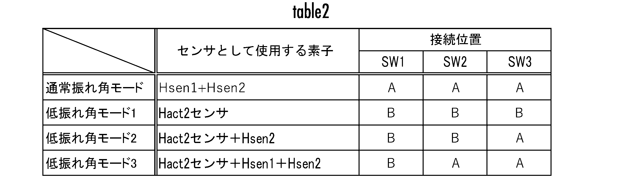
図6A及び図6Bは、低振れ角モードを低振れ角モード1とする外付け回路においてそれぞれ第1駆動期間及び第2駆動期間の状態図である。図7は、外付け回路における第1駆動期間及び第2駆動期間の波形図である。なお、低振れ角モード1は、(b1)の検出方式に対応する。
図6A及び図6Bにおいて、制御部45は、SW(スイッチ)1ーSW3の接続位置を制御する。66,67は、駆動アンプである。68-71は、センサアンプである。75,76は、抵抗である。
制御部45は、第1駆動電圧及び第2駆動電圧をそれぞれ駆動アンプ66,67を介して第1組39及び第2組40に供給する。第2組40及び圧電センサ43aの出力電圧は、センサアンプ68,69を介して制御部45に送られる。圧電センサ43bの出力電圧は、センサアンプ70,71を介して制御部45に送られる。
SW1は、第1駆動期間(図6A)、すなわち第2組40を圧電アクチュエータで使用するときには、第2組40を接点Aに接続し、第2駆動期間(図6B)、すなわち第2組40を圧電センサで使用するときは、第2組40を接点Bに接続する。SW2,SW3は、第1駆動期間及び第2駆動期間にはそれぞれ共に接点A及び接点Bの接続位置になる。
図7において、時間t=t1を境にHアクチュエータ33の駆動期間は、第1駆動期間から第2駆動期間に切り替えられる。SW1-SW3の2値レベルにおいて、”0”は接続位置が接点Aにあることを示し、”1“は接続位置が接点Bにあることを示している。
第1駆動期間において、第1駆動電圧及び第2駆動電圧は、相互に逆位相の駆動電圧になっている。これにより、ミラー部31は、第1軸の回りを大きな振れ角幅で往復回動する。すなわち、走査光ビームLsは、H方向に大きな走査幅で走査する。
圧電センサ43a,43bは、相互に逆位相で湾曲変形し、第1駆動期間では、相互に逆位相の出力電圧を生成している。制御部45(詳しくは、制御部45の検出部50)は、第1駆動期間では、圧電センサ43bの出力電圧を反転してから、圧電センサ43aの出力電圧に加算し、加算後の値(図4の“◇”参照)に基づき第1駆動期間の振れ角γを検出する。第1駆動期間における振れ角幅は十分大きいので、振れ角γの検出精度は十分に保証される。
第2駆動期間において、SW1,SW2は、共に接点Bの接続位置になる。これにより、Hアクチュエータ33は、第1組39の圧電区画部分のみにより、ミラー部31を第1軸の回りに往復回動させる。このため、Hアクチュエータ33によるアクチュエータ力は、半減するが、第2駆動期間は、第1軸の回りにミラー部31を小さい振れ角幅で往復動させる期間であり、ミラー部31は、第1軸の回りに指示された振れ角幅で支障なく往復回動する。
一方、第2駆動期間では、SW1ーSW3の全部が接点Bの接続位置になる。これにより、第2組40の圧電区画部分の出力電圧が制御部45に送られる。制御部45の検出部50は、第2組40の圧電区画部分の出力電圧に基づき振れ角γを検出する。第2組40の圧電区画部分の出力電圧は、圧電センサ43a,43bの加算値の出力電圧より大きいので(図4の“□”と“◇”との対比参照)、検出部50は、十分な精度で振れ角γを検出することができる。また、第2組40の圧電区画部分42b、42d、42fは、いずれも圧電センサ43a,43bと比べてトーションバー32bから離間している場所に位置するため、トーションバーから応力がかかりすぎて剥離することが防がれる。
図5のフローチャートを説明する。S(ステップ)101では、駆動部49は、ミラー部31を第1軸の回りに往復回動させる振れ角モードを判定する。振れ角モードには、低振れ角モードと高振れ角モードとの2つがある。具体的には、駆動部49は、ミラー部31を、振れ角γの振れ角幅を閾値γa以下にして往復回動させるときは、低振れ角モードの制御期間と判定し、振れ角γの振れ角幅を閾値γaより大きくして往復回動させるときは、高振れ角モードの制御期間と判定する。
駆動部49は、低振れ角モードの制御期間と判定したときは、処理をS102に進める。駆動部49は、高振れ角モードの制御期間と判定したときは、処理をS108に進める。
先に、低振れ角モードの制御期間の処理について説明する。S102において、駆動部49は、第2駆動電圧の出力を停止して、第1駆動電圧のみを出力し、第1組39の圧電区画部分のみを駆動する。この結果、ミラー部31のアクチュエータ力は、半減するが、この期間のミラー部31に要求されている振れ角γの振れ角幅は小さいので、第1軸の回りのミラー部31の往復回動には支障がない。
S103において、接続切替部51は、圧電センサ43a,43bをアースに接続する。具体的には、接続切替部51は、図6Bに図示されているように、SW1-SW3の接続位置をすべて接点Bに切り替える。この結果、圧電センサ43a,43bの出力端子は、0V(アース)に維持され、湾曲変形中の電荷蓄積による脱分極が防止される。
一方、SW1の接続位置が接点Aから接点Bに切替わることに伴い、第2組40の機能は、圧電アクチュエータから圧電センサに切り替わる。
S104において、検出部50は、第2組40の圧電区画部分の出力電圧Voa2に基づき振れ角γを検出する。図4の“□”で説明したように、ミラー部31は低振れ角モードであるにもかかわらず、検出部50の出力電圧は、十分な大きさを確保される。したがって、低振れ角モード時の振れ角γの検出精度が保証される。
高振れ角モードの制御期間の処理について説明する。S108において、駆動部49は、第1出力電圧及び第2出力電圧の両方でそれぞれ第1組39及び第2組40を駆動する。なお、高振れ角モードの制御期間では、接続切替部51は、SW1-SW3の全部を接点Aに切り替えている(図6B)。
Hアクチュエータ33において、第1組39及び第2組40の両方の圧電区画部分が駆動されることにより、Hアクチュエータ33は、大きなアクチュエータ力を出力する。これにより、ミラー部31は、第1軸の回りの大きな振れ角幅で往復回動することができる。
S109において、検出部50は、圧電センサ43a,43bの出力電圧Vos1,Vos2の加算値に基づき振れ角γを検出する。図4の“◇”で説明したように、高振れ角モード時の振れ角γの振れ角幅は大きい。したがって、高振れ角モード時の振れ角γの検出精度が保証される。
(その他の低振れ角モード)
図8Aは、低振れ角モードを低振れ角モード2とする外付け回路において第2駆動期間の接続状態を示す図である。なお、低振れ角モード2は、(b2)の検出方式に対応する。
図8Aは、低振れ角モードを低振れ角モード2とする外付け回路において第2駆動期間の接続状態を示す図である。なお、低振れ角モード2は、(b2)の検出方式に対応する。
図8Bは、図8Aの外付け回路における第2駆動期間の波形図である。なお、図8Aの制御部45における第1駆動期間の接続位置は、図6Aと同一であるので、図示は省略する。また、図8Aの制御部45における第1駆動期間の第1組39、SW1,SW2及び圧電センサ43aの波形図は、図7のそれらとの波形図と同一であるので、図示は省略する。
図8A及び図8Bにおいて、図6B及び図7との相違点について説明する。図8Aの第2駆動期間では、SW3は、接点Aの接続位置になる。これにより、検出部50は、第2組40の圧電区画部分の出力電圧と圧電センサ43bの出力電圧との加算値に基づき振れ角γを検出する。
圧電センサ43bの出力電圧は、第2組40の圧電区画部分の出力電圧とは逆位相の関係にある。したがって、検出部50は、圧電センサ43bの出力電圧を反転してから第2組40の圧電区画部分の出力電圧に加算する。
図9Aは、低振れ角モードを低振れ角モード3とする外付け回路において第2駆動期間の接続状態を示す図である。低振れ角モード3は、(b3)の検出方式に対応する。図9Bは、図9Aの外付け回路の波形図である。なお、図9Aの制御部45における第1駆動期間の接続位置は、図6Aと同一であるので、図示は省略する。また、図9Bの制御部45における第1駆動期間の第1組39、SW1,SW2及び圧電センサ43aの波形図は、図7のそれらの波形図と同一であるので、図示は省略する。
図9A及び図9Bにおいて、図6B及び図7との相違点について説明する。圧電センサ43aは、第2組40の圧電区画部分用のセンサアンプ68,69とは別に専用のセンサアンプ77,78が用意される。
図9Aの第2駆動期間では、SW2、SW3は、共に、接続位置を接点Aに切り替えている。これにより、検出部50は、第2組40の圧電区画部分の出力電圧と圧電センサ43a,43bの出力電圧の加算値との加算値に基づき振れ角γを検出する。
図10は、第2駆動期間に駆動組及び非駆動組を交互に切り替える駆動方式の回路図である。第2駆動期間の駆動組及び非駆動組を、以下、それぞれ第1組39及び第2組40とする第1動作期間と、第2組40及び第1組39とする第2動作期間とに分けられる。図11は、図10の回路において各動作期間の波形を対比して示す図である。
図10において、SW6,SW7は、制御部45からの制御信号により接続位置が切り替えられる。
図10の上側の図及び図11の左半部は、第1動作期間の接続位置及び波形を示し、図10の下側の図及び図11の右半部は、第2動作期間の接続位置及び波形を示している。第1動作期間と第2動作期間とは、第2駆動期間において、例えば一定時間間隔で交互に切り替えられる。
第1動作期間では、SW6,SW7の接続位置は共に接点Aになっている。これにより、第1駆動電圧が第1組39に供給される一方、第2組40への第2駆動電圧の供給は停止される。これにより、Hアクチュエータ33は、第1組39の圧電区画部分のみが圧電アクチュエータとして作動する一方、第2組40の圧電区画部分は、圧電センサとして振れ角γに係る出力電圧を出力する。さらに、検出部50には、第2組40からの出力電圧と共に、圧電センサ43a,43bからの出力電圧が入力され、検出部50は、これら3個の素子(圧電体)からの出力電圧に基づいて振れ角γを検出する。
第2動作期間では、SW6,SW7の接続位置が共に接点Bに切り替えられる。これにより、第1組39への駆動部49からの第1駆動電圧の供給が停止される一方、駆動部49から第2組40への第2駆動電圧の供給は実施される。この結果、Hアクチュエータ33は、第2組40の圧電区画部分のみが圧電アクチュエータとして作動する一方、第1組39は、圧電センサとして振れ角γに係る出力電圧を出力する。さらに、検出部50には、第1組39からの出力電圧と共に、圧電センサ43a,43bからの出力電圧が入力され、検出部50は、これら3個の素子(圧電体)からの出力電圧に基づいて振れ角γを検出する。
この実施形態では、第2駆動期間において駆動組及び非駆動組を第1組39及び第2組40間で交互に切り替えることにより、各圧電区画部分は圧電アクチュエータの作動と停止とを交互に繰り返すので、寿命が改善される。
(変形例)
実施形態の光偏向器30では、Hアクチュエータ33がトーションバー32と結合する2つの結合部分の少なくとも一方の結合部分(例:トーションバー32b側の結合部分)において、第1軸の両側に圧電センサ43の対が設けられている。本発明では、他方の結合部分(例:トーションバー32a側の結合部分)にも圧電センサ43の対を設けて、2対の圧電センサ43に出力電圧から振れ角γを検出することも可能である。
実施形態の光偏向器30では、Hアクチュエータ33がトーションバー32と結合する2つの結合部分の少なくとも一方の結合部分(例:トーションバー32b側の結合部分)において、第1軸の両側に圧電センサ43の対が設けられている。本発明では、他方の結合部分(例:トーションバー32a側の結合部分)にも圧電センサ43の対を設けて、2対の圧電センサ43に出力電圧から振れ角γを検出することも可能である。
実施形態の光偏向器30は、2軸式の光偏向器となっている。本発明の光走査装置が装備する光偏向器は、1軸式の光偏向器であってもよい。
実施形態のHアクチュエータ33は、環状に形成されている。本発明の光走査装置が装備する圧電アクチュエータは、特許文献1のような各トーションバーの両側に結合する直線状(非環状)の圧電アクチュエータであってもよい。
実施形態の図4では、振れ角γの検出の基にする出力電圧の組み合わせとして、Hact2センサ+Hsen2の1つのみとなっている。本発明の組み合わせは、その他として、(c1)Hact2センサ+Hsen1、(c2)Hact2センサ+Hsen1+Hsen2、(c3)Hact2センサ+Hsen2、(c4)Hact1センサ+Hsen1、及び、(c5)Hact1センサ+Hsen1+Hsen2のいずれかの組み合わせにしてよい。
実施形態では、支持部としての可動枠34は、ミラー部31を包囲する環状になっている。本発明では、支持部は、ミラー部を外側から包囲する環状でなくてもよい。本発明の支持部は、ミラー部を片側から支持する構造であってもよい。
10・・・光走査装置、20・・・レーザ光源、30・・・光偏向器、31・・・ミラー部、32a,32b・・・トーションバー、33・・・Hアクチュエータ(環状圧電アクチュエータ)、34・・・可動枠(支持部)、39・・・第1組、40・・・第2組、42a-42f・・圧電区画部分、43a,43b・・・圧電センサ、45・・・制御部、49・・・駆動部、50・・・検出部、51・・・接続切替部。
Claims (6)
- ミラー部、支持部、及び、直列に結合された複数の圧電区画部分を有し、前記支持部と前記ミラー部との間に介在し、前記ミラー部を回転軸の回りに往復回動させる圧電アクチュエータを含む光偏向器と、
前記複数の圧電区画部分を前記光偏向器の基端側から作用端側に並び順に交互に第1組と第2組とに組分けしたとき、前記第1組及び前記第2組の圧電区画部分に対し相互に逆位相の関係になる位相で第1駆動電圧及び第2駆動電圧をそれぞれ供給する駆動部と、
前記回転軸の回りの前記ミラー部の振れ角を検出する検出部と、
を備え、
前記駆動部は、
第1駆動期間では、前記第1組及び前記第2組の両方の組の圧電区画部分に対し駆動電圧を供給し、
第2駆動期間では、前記第1組及び前記第2組の一方の組の圧電区画部分に対してのみ駆動電圧を供給し、
前記検出部は、前記第2駆動期間には、他方の組の圧電区画部分の出力電圧に基づいて前記振れ角を検出することを特徴とする光走査装置。 - 請求項1記載の光走査装置において、
前記支持部は、前記ミラー部を環状に包囲し、
前記光偏向器は、前記ミラー部の両側から延び出して前記支持部に結合する1対のトーションバーを有し、
前記圧電アクチュエータは、前記支持部の内周側において前記ミラー部を環状に包囲し、前記回転軸としての第1軸の軸上で前記1対のトーションバーの中間部に結合し、前記ミラー部の中心で前記第1軸に対して直交する第2軸上で前記支持部に結合している環状圧電アクチュエータであることを特徴とする光走査装置。 - 請求項2記載の光走査装置において、
さらに、前記1対のトーションバーに結合する前記環状圧電アクチュエータの結合部分の少なくとも一方の結合部分において前記第1軸を両側から挟んで配置された1対の圧電センサを備え、
前記検出部は、前記第1駆動期間には前記1対の圧電センサの出力電圧に基づいて前記振れ角を検出することを特徴とする光走査装置。 - 請求項3記載の光走査装置において、
前記検出部は、前記第2駆動期間には、前記他方の組の前記圧電区画部分の出力電圧と、前記1対の圧電センサの出力電圧との加算に基づいて前記振れ角を検出することを特徴とする光走査装置。 - 請求項3又は4記載の光走査装置において、
さらに、前記第2駆動期間に、前記1対の圧電センサの少なくとも一方の出力端子を、アースに接続する接続切替部を備えることを特徴とする光走査装置。 - 請求項5記載の光走査装置において、
前記接続切替部は、前記第2駆動期間において、前記他方の組を前記第1組及び第2組間で交互に切り替えることを特徴とする光走査装置。
Priority Applications (3)
| Application Number | Priority Date | Filing Date | Title |
|---|---|---|---|
| US17/922,322 US12360362B2 (en) | 2020-05-25 | 2021-03-19 | Optical scanning device |
| EP21812062.4A EP4130846B1 (en) | 2020-05-25 | 2021-03-19 | Optical scanning device |
| CN202180035895.0A CN115668029A (zh) | 2020-05-25 | 2021-03-19 | 光扫描装置 |
Applications Claiming Priority (2)
| Application Number | Priority Date | Filing Date | Title |
|---|---|---|---|
| JP2020090522A JP7420645B2 (ja) | 2020-05-25 | 2020-05-25 | 光走査装置 |
| JP2020-090522 | 2020-05-25 |
Publications (1)
| Publication Number | Publication Date |
|---|---|
| WO2021240965A1 true WO2021240965A1 (ja) | 2021-12-02 |
Family
ID=78723331
Family Applications (1)
| Application Number | Title | Priority Date | Filing Date |
|---|---|---|---|
| PCT/JP2021/011400 Ceased WO2021240965A1 (ja) | 2020-05-25 | 2021-03-19 | 光走査装置 |
Country Status (5)
| Country | Link |
|---|---|
| US (1) | US12360362B2 (ja) |
| EP (1) | EP4130846B1 (ja) |
| JP (1) | JP7420645B2 (ja) |
| CN (1) | CN115668029A (ja) |
| WO (1) | WO2021240965A1 (ja) |
Families Citing this family (3)
| Publication number | Priority date | Publication date | Assignee | Title |
|---|---|---|---|---|
| CN114105081A (zh) * | 2020-08-27 | 2022-03-01 | 中光电智能感测股份有限公司 | 微型扫描面镜 |
| JP7751997B2 (ja) * | 2021-07-13 | 2025-10-09 | スタンレー電気株式会社 | Mems光偏向器及び光走査装置 |
| TWI857576B (zh) * | 2023-04-25 | 2024-10-01 | 中光電智能感測股份有限公司 | 壓電致動裝置 |
Citations (6)
| Publication number | Priority date | Publication date | Assignee | Title |
|---|---|---|---|---|
| JP2008178173A (ja) * | 2007-01-16 | 2008-07-31 | Seiko Epson Corp | アクチュエータ、光スキャナおよび画像形成装置 |
| JP4984117B2 (ja) | 2006-07-13 | 2012-07-25 | スタンレー電気株式会社 | 2次元光スキャナ、それを用いた光学装置および2次元光スキャナの製造方法 |
| JP2012154989A (ja) * | 2011-01-24 | 2012-08-16 | Stanley Electric Co Ltd | 光偏向モジュール |
| JP5493735B2 (ja) | 2009-01-30 | 2014-05-14 | 株式会社リコー | 偏向ミラー、光走査装置、画像形成装置、および画像投影装置 |
| JP6092713B2 (ja) | 2013-05-28 | 2017-03-08 | スタンレー電気株式会社 | 光偏向器 |
| CN108761773A (zh) * | 2018-06-15 | 2018-11-06 | 重庆大学 | 一种压电非均匀折叠梁驱动的moems扫描光栅微镜 |
Family Cites Families (9)
| Publication number | Priority date | Publication date | Assignee | Title |
|---|---|---|---|---|
| JP2004163551A (ja) * | 2002-11-12 | 2004-06-10 | Olympus Corp | 撮像装置及びその制御方法 |
| CN103620477B (zh) * | 2012-02-22 | 2015-04-29 | 京瓷办公信息系统株式会社 | 光扫描装置和图像形成装置 |
| JP6092595B2 (ja) | 2012-11-27 | 2017-03-08 | スタンレー電気株式会社 | 光偏向器 |
| JP2015169745A (ja) * | 2014-03-06 | 2015-09-28 | スタンレー電気株式会社 | 光偏向器 |
| WO2016052548A1 (ja) * | 2014-09-30 | 2016-04-07 | 富士フイルム株式会社 | ミラー駆動装置及びその駆動方法 |
| JP6493014B2 (ja) * | 2015-06-25 | 2019-04-03 | 株式会社デンソー | 光走査装置 |
| JP6974696B2 (ja) * | 2017-04-28 | 2021-12-01 | ミツミ電機株式会社 | 光走査装置 |
| JP7108477B2 (ja) * | 2018-06-21 | 2022-07-28 | スタンレー電気株式会社 | 光偏向器 |
| JP7048443B2 (ja) * | 2018-07-19 | 2022-04-05 | スタンレー電気株式会社 | 光投射装置 |
-
2020
- 2020-05-25 JP JP2020090522A patent/JP7420645B2/ja active Active
-
2021
- 2021-03-19 WO PCT/JP2021/011400 patent/WO2021240965A1/ja not_active Ceased
- 2021-03-19 CN CN202180035895.0A patent/CN115668029A/zh active Pending
- 2021-03-19 EP EP21812062.4A patent/EP4130846B1/en active Active
- 2021-03-19 US US17/922,322 patent/US12360362B2/en active Active
Patent Citations (6)
| Publication number | Priority date | Publication date | Assignee | Title |
|---|---|---|---|---|
| JP4984117B2 (ja) | 2006-07-13 | 2012-07-25 | スタンレー電気株式会社 | 2次元光スキャナ、それを用いた光学装置および2次元光スキャナの製造方法 |
| JP2008178173A (ja) * | 2007-01-16 | 2008-07-31 | Seiko Epson Corp | アクチュエータ、光スキャナおよび画像形成装置 |
| JP5493735B2 (ja) | 2009-01-30 | 2014-05-14 | 株式会社リコー | 偏向ミラー、光走査装置、画像形成装置、および画像投影装置 |
| JP2012154989A (ja) * | 2011-01-24 | 2012-08-16 | Stanley Electric Co Ltd | 光偏向モジュール |
| JP6092713B2 (ja) | 2013-05-28 | 2017-03-08 | スタンレー電気株式会社 | 光偏向器 |
| CN108761773A (zh) * | 2018-06-15 | 2018-11-06 | 重庆大学 | 一种压电非均匀折叠梁驱动的moems扫描光栅微镜 |
Non-Patent Citations (1)
| Title |
|---|
| See also references of EP4130846A4 |
Also Published As
| Publication number | Publication date |
|---|---|
| JP7420645B2 (ja) | 2024-01-23 |
| US20230168490A1 (en) | 2023-06-01 |
| EP4130846A1 (en) | 2023-02-08 |
| JP2021189189A (ja) | 2021-12-13 |
| EP4130846B1 (en) | 2024-09-25 |
| EP4130846A4 (en) | 2023-09-06 |
| US12360362B2 (en) | 2025-07-15 |
| CN115668029A (zh) | 2023-01-31 |
Similar Documents
| Publication | Publication Date | Title |
|---|---|---|
| WO2021240965A1 (ja) | 光走査装置 | |
| US10371940B2 (en) | Mirror driving device and driving method thereof | |
| US10281716B2 (en) | Mirror driving device and driving method thereof | |
| US7697185B2 (en) | Actuator, optical scanner and image forming device | |
| US20130208330A1 (en) | Mirror driving device and method of controlling the device | |
| EP2808719B1 (en) | Optical deflector including separated piezoelectric portions on piezoelectric actuators | |
| US20130107339A1 (en) | Optical reflection element | |
| JP5990917B2 (ja) | Memsデバイスおよびプロジェクタ機能を有する電子機器 | |
| US9097897B2 (en) | Optical deflector including narrow piezoelectric sensor element between torsion bar and piezoelectric actuator | |
| US20120250127A1 (en) | Mirror driving device and mirror driving method | |
| US20110122471A1 (en) | Piezoelectric actuator, optical reflection element using the same and piezoelectric driver | |
| JP2012237788A (ja) | 光走査装置およびそれを備えた画像投影装置 | |
| US11054634B2 (en) | Optical scanning apparatus and method of controlling optical scanning apparatus | |
| US12007556B2 (en) | Light deflection device | |
| US10394018B2 (en) | Optical scanning device | |
| US20240288681A1 (en) | Mems optical deflector and optical scanning device | |
| JP6808506B2 (ja) | 光走査装置 | |
| CN111830701B (zh) | 电磁微镜及激光设备 | |
| JP6189137B2 (ja) | 光スキャナ | |
| JP2008111882A (ja) | アクチュエータ、光スキャナおよび画像形成装置 | |
| US10048490B2 (en) | Drive system, video device, image projection device, and drive control method | |
| JP2020148994A (ja) | 光走査装置 | |
| JP2017040911A (ja) | 駆動システム、映像機器、画像投影装置および駆動制御方法 | |
| CN120871424A (zh) | 用于微机电系统反射镜的加强结构和固定结构 | |
| JP2021101219A (ja) | 回転装置、光偏向装置、表示システムおよび移動体 |
Legal Events
| Date | Code | Title | Description |
|---|---|---|---|
| 121 | Ep: the epo has been informed by wipo that ep was designated in this application |
Ref document number: 21812062 Country of ref document: EP Kind code of ref document: A1 |
|
| ENP | Entry into the national phase |
Ref document number: 2021812062 Country of ref document: EP Effective date: 20221027 |
|
| NENP | Non-entry into the national phase |
Ref country code: DE |
|
| WWG | Wipo information: grant in national office |
Ref document number: 17922322 Country of ref document: US |