WO2021241054A1 - 電力変換装置の制御装置及び制御方法 - Google Patents
電力変換装置の制御装置及び制御方法 Download PDFInfo
- Publication number
- WO2021241054A1 WO2021241054A1 PCT/JP2021/015556 JP2021015556W WO2021241054A1 WO 2021241054 A1 WO2021241054 A1 WO 2021241054A1 JP 2021015556 W JP2021015556 W JP 2021015556W WO 2021241054 A1 WO2021241054 A1 WO 2021241054A1
- Authority
- WO
- WIPO (PCT)
- Prior art keywords
- power
- conversion device
- power conversion
- converter
- circulating current
- Prior art date
- Legal status (The legal status is an assumption and is not a legal conclusion. Google has not performed a legal analysis and makes no representation as to the accuracy of the status listed.)
- Ceased
Links
Images









Classifications
-
- H—ELECTRICITY
- H02—GENERATION; CONVERSION OR DISTRIBUTION OF ELECTRIC POWER
- H02M—APPARATUS FOR CONVERSION BETWEEN AC AND AC, BETWEEN AC AND DC, OR BETWEEN DC AND DC, AND FOR USE WITH MAINS OR SIMILAR POWER SUPPLY SYSTEMS; CONVERSION OF DC OR AC INPUT POWER INTO SURGE OUTPUT POWER; CONTROL OR REGULATION THEREOF
- H02M7/00—Conversion of AC power input into DC power output; Conversion of DC power input into AC power output
- H02M7/42—Conversion of DC power input into AC power output without possibility of reversal
- H02M7/44—Conversion of DC power input into AC power output without possibility of reversal by static converters
- H02M7/48—Conversion of DC power input into AC power output without possibility of reversal by static converters using discharge tubes with control electrode or semiconductor devices with control electrode
- H02M7/483—Converters with outputs that each can have more than two voltages levels
- H02M7/4835—Converters with outputs that each can have more than two voltages levels comprising two or more cells, each including a switchable capacitor, the capacitors having a nominal charge voltage which corresponds to a given fraction of the input voltage, and the capacitors being selectively connected in series to determine the instantaneous output voltage
-
- H—ELECTRICITY
- H02—GENERATION; CONVERSION OR DISTRIBUTION OF ELECTRIC POWER
- H02M—APPARATUS FOR CONVERSION BETWEEN AC AND AC, BETWEEN AC AND DC, OR BETWEEN DC AND DC, AND FOR USE WITH MAINS OR SIMILAR POWER SUPPLY SYSTEMS; CONVERSION OF DC OR AC INPUT POWER INTO SURGE OUTPUT POWER; CONTROL OR REGULATION THEREOF
- H02M1/00—Details of apparatus for conversion
- H02M1/08—Circuits specially adapted for the generation of control voltages for semiconductor devices incorporated in static converters
-
- H—ELECTRICITY
- H02—GENERATION; CONVERSION OR DISTRIBUTION OF ELECTRIC POWER
- H02M—APPARATUS FOR CONVERSION BETWEEN AC AND AC, BETWEEN AC AND DC, OR BETWEEN DC AND DC, AND FOR USE WITH MAINS OR SIMILAR POWER SUPPLY SYSTEMS; CONVERSION OF DC OR AC INPUT POWER INTO SURGE OUTPUT POWER; CONTROL OR REGULATION THEREOF
- H02M1/00—Details of apparatus for conversion
- H02M1/12—Arrangements for reducing harmonics from AC input or output
- H02M1/123—Suppression of common mode voltage or current
-
- H—ELECTRICITY
- H02—GENERATION; CONVERSION OR DISTRIBUTION OF ELECTRIC POWER
- H02M—APPARATUS FOR CONVERSION BETWEEN AC AND AC, BETWEEN AC AND DC, OR BETWEEN DC AND DC, AND FOR USE WITH MAINS OR SIMILAR POWER SUPPLY SYSTEMS; CONVERSION OF DC OR AC INPUT POWER INTO SURGE OUTPUT POWER; CONTROL OR REGULATION THEREOF
- H02M7/00—Conversion of AC power input into DC power output; Conversion of DC power input into AC power output
- H02M7/42—Conversion of DC power input into AC power output without possibility of reversal
- H02M7/44—Conversion of DC power input into AC power output without possibility of reversal by static converters
- H02M7/48—Conversion of DC power input into AC power output without possibility of reversal by static converters using discharge tubes with control electrode or semiconductor devices with control electrode
- H02M7/53—Conversion of DC power input into AC power output without possibility of reversal by static converters using discharge tubes with control electrode or semiconductor devices with control electrode using devices of a triode or transistor type requiring continuous application of a control signal
- H02M7/537—Conversion of DC power input into AC power output without possibility of reversal by static converters using discharge tubes with control electrode or semiconductor devices with control electrode using devices of a triode or transistor type requiring continuous application of a control signal using semiconductor devices only, e.g. single switched pulse inverters
- H02M7/5387—Conversion of DC power input into AC power output without possibility of reversal by static converters using discharge tubes with control electrode or semiconductor devices with control electrode using devices of a triode or transistor type requiring continuous application of a control signal using semiconductor devices only, e.g. single switched pulse inverters in a bridge configuration
- H02M7/53871—Conversion of DC power input into AC power output without possibility of reversal by static converters using discharge tubes with control electrode or semiconductor devices with control electrode using devices of a triode or transistor type requiring continuous application of a control signal using semiconductor devices only, e.g. single switched pulse inverters in a bridge configuration with automatic control of output voltage or current
-
- H—ELECTRICITY
- H02—GENERATION; CONVERSION OR DISTRIBUTION OF ELECTRIC POWER
- H02M—APPARATUS FOR CONVERSION BETWEEN AC AND AC, BETWEEN AC AND DC, OR BETWEEN DC AND DC, AND FOR USE WITH MAINS OR SIMILAR POWER SUPPLY SYSTEMS; CONVERSION OF DC OR AC INPUT POWER INTO SURGE OUTPUT POWER; CONTROL OR REGULATION THEREOF
- H02M7/00—Conversion of AC power input into DC power output; Conversion of DC power input into AC power output
- H02M7/42—Conversion of DC power input into AC power output without possibility of reversal
- H02M7/44—Conversion of DC power input into AC power output without possibility of reversal by static converters
- H02M7/48—Conversion of DC power input into AC power output without possibility of reversal by static converters using discharge tubes with control electrode or semiconductor devices with control electrode
- H02M7/53—Conversion of DC power input into AC power output without possibility of reversal by static converters using discharge tubes with control electrode or semiconductor devices with control electrode using devices of a triode or transistor type requiring continuous application of a control signal
- H02M7/537—Conversion of DC power input into AC power output without possibility of reversal by static converters using discharge tubes with control electrode or semiconductor devices with control electrode using devices of a triode or transistor type requiring continuous application of a control signal using semiconductor devices only, e.g. single switched pulse inverters
- H02M7/539—Conversion of DC power input into AC power output without possibility of reversal by static converters using discharge tubes with control electrode or semiconductor devices with control electrode using devices of a triode or transistor type requiring continuous application of a control signal using semiconductor devices only, e.g. single switched pulse inverters with automatic control of output wave form or frequency
- H02M7/5395—Conversion of DC power input into AC power output without possibility of reversal by static converters using discharge tubes with control electrode or semiconductor devices with control electrode using devices of a triode or transistor type requiring continuous application of a control signal using semiconductor devices only, e.g. single switched pulse inverters with automatic control of output wave form or frequency by pulse-width modulation
Definitions
- the present invention relates to a control device and a control method for a power converter configured by a modular multi-level converter (hereinafter, abbreviated as MMC converter).
- MMC converter modular multi-level converter
- the MMC converter is configured by connecting a voltage source such as a capacitor, which is an energy storage element, and a plurality of unit converters composed of a half-bridge circuit in series.
- the unit converter generates a desired voltage by controlling the PWM modulation factor of the half-bridge circuit.
- Multiple unit converters are connected in series to form a two-terminal arm converter, the first terminal of this arm converter is connected to each phase terminal of the AC power supply, and the second terminal connected in a star shape is DC. Connect to the power terminal.
- the arm converter connected to each phase in this way generates a desired AC voltage and controls the AC current, and at the same time, superimposes the DC current to realize power conversion with the DC power supply.
- the control of the MMC converter is the current control that adjusts the arm current flowing through the arm converter to the AC current command and DC current command from the outside, and keeps the total stored energy of the capacitor in the arm converter balanced between the arm converters.
- the function to adjust the circulating current for the purpose (hereinafter referred to as circulating current control), the average voltage of the capacitor is adjusted between the unit converters by mutually adjusting the PWM modulation rate of the half bridge circuit provided in the unit converter in the arm. It is equipped with a function to maintain balance (hereinafter referred to as interstage balance control).
- interstage balance control a function to maintain balance
- Patent Document 1 discloses a double-star MMC converter (hereinafter, abbreviated as DSMMC converter), which is a form of an MMC converter. According to Patent Document 1, it is disclosed that the circulating current flowing between the arm converters can be suppressed by providing an inductance between the first terminal of each arm converter and the AC power supply terminal. Further, it is disclosed that the circulating current of the secondary harmonic is used for the purpose of balancing the total stored energy of the capacitors in the arm converter between the arm converters.
- the present invention targets a control method for a power conversion device including a DSMMC converter as disclosed in Patent Document 1.
- the voltage of the capacitor in the unit converter fluctuates by repeating charging and discharging at a cycle determined by the output AC frequency of the DSMMC converter.
- a large current flows through each unit converter, so that the capacitor voltage fluctuates greatly.
- the peak voltage value of the voltage fluctuation becomes high, it is necessary to increase the voltage rating of the capacitor, and there is a problem that the DSMMC converter becomes large.
- the circulating current is the current that circulates inside the arm converter without flowing to either the AC power supply or the DC power supply.
- the role of the power converter is to realize power conversion between a plurality of different power sources. Therefore, in order to realize a highly efficient power conversion device, it is desirable that the circulating current can be minimized.
- Patent Document 1 does not disclose a specific means for determining the circulating current.
- Patent Document 2 discloses a means for reducing the voltage fluctuation amount of a capacitor by generating a circulating current command value of secondary tuning from an AC current command value.
- the power converter since the power converter generates a desired AC power by the phase difference between the output AC voltage and the AC current, the capacitor voltage fluctuation waveform of the DSMMC converter changes depending on the power factor of the power converter. Therefore, it is desirable to generate the required circulating current in consideration of the power factor in order to realize a highly efficient power conversion device, but Patent Document 2 still has a problem that such means is not provided. ..
- an object of the present invention is to solve the above-mentioned problems and to provide a control device and a control method for a highly efficient power conversion device.
- the present invention is a control device for a modular multi-level power converter equipped with one or more arm converters in which a plurality of unit converters equipped with energy storage elements are connected in series for each phase of alternating current.
- the control device of the power converter uses an AC current control means that feedback-controls the AC current to a desired value and a circulating current command that flows through the arm converter of each phase of the AC of the modular multi-level power converter.
- the gate of the unit converter that constitutes the arm converter according to the AC voltage target of each AC phase obtained by correcting the output of the circulating current control means for feedback control to the value and the output of the AC current control means with the output of the circulating current control means.
- the PWM command generating means for generating and controlling a signal is provided, and the circulating current control means is provided with a circulating current command calculating means for calculating the amplitude of the circulating current command value according to the power factor of the power conversion device. It is a control device for a power conversion device.
- a control method for a modular multi-level power converter having one or more arm converters in which a plurality of unit converters having energy storage elements are connected in series for each phase of alternating current is provided, and is an alternating current.
- the AC current control output that feedback-controls to the desired value is corrected by the circulating current control output that feedback-controls the circulating current flowing through the arm converter of each phase of the AC of the modular multi-level power converter to the circulating current command value.
- the gate signal of the unit converter that constitutes the arm converter is generated and controlled according to the AC voltage target of each AC phase obtained in the above process, and the amplitude of the circulating current command value is determined according to the power factor of the power converter.
- the necessary circulating current is generated in consideration of the power factor, it is possible to provide a control device and a method for a highly efficient power conversion device.
- the figure which shows the operation waveform example at the time of COS ⁇ 0 (inductive).
- the figure which shows the operation waveform example when COS ⁇ 1.
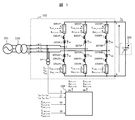
- FIG. 1 is a diagram showing a configuration example of a general power conversion device to which the present invention can be applied.
- the power conversion device 102 is connected to the AC power system 101 via the transformer 104.
- the power conversion device 102 is connected to the variable DC voltage source 103. With this configuration, power interchange between the AC power system 101 and the variable DC voltage source 103 can be realized.
- the power converter 102 is composed of a DSMMC converter.
- the power converter 102 is composed of six sets of arms in which the arm converter 105 and the reactor 106 are connected in series, so-called Grate connection.
- the power converter 102 includes six arm converters 105 (105UP, 105UN, 105VP, 105VN, 105WP, 105WN) having two output terminals, a terminal and b terminal, and six circulating current suppression reactors. It is basically composed of 106 (106UP, 106UN, 106VP, 106VN, 106WP, 106WN), and the arm currents I (I UP , I UN , I VP , I) of each phase are obtained in order to obtain a signal for control.
- VN and includes I WP, 6 one current detector 107 (107UP for detecting I WN), 107UN, 107VP, 107VN, 107WP, the 107WN).
- Controller 108 an arm current six current detector 107, the output AC voltage V G of the power conversion device 102 from the AC voltage detector 109 (V GU, V GV, V GW) by detecting the type , Gives a gate control signal g for the six arm converters 105.
- each phase of the alternating current is represented by U, V, and W, and a symbol is added with the positive and negative of the DC circuit as PN.
- the various signal lines indicated by 3, 6, and 3N indicate the total number of signal lines described by one.
- the b terminal of the positive arm converters 105UP, 105VP, 105WP and the a terminal of the negative arm converters 105UN, 105VN, 105WN are the circulating current suppression reactor 106 (106UP, 106UN). , 106VP, 106VN, 106WP, 106WN) to connect to the AC power supply terminal (U terminal, V terminal, W terminal).
- the a terminal of the positive arm converters 105UP, 105VP, 105WP and the b terminal of the negative arm converters 105UN, 105VN, 105WN are connected to the positive and negative DC terminals (P terminal, N terminal).
- the variable DC voltage source 103 is also connected to the DC terminal.
- FIG. 2 is a diagram showing a configuration example of a general arm converter to which the present invention can be applied.
- the arm converter 105UP will be described as a representative, but since the other arm converters 105UN, 105VP, 105VN, 105WP, and 105WN have the same configuration, the description of the other arm converters will be omitted.
- the arm converter 105UP is a circuit in which N unit converters 200 (200_1 to 200_N) are connected in series.
- the unit converter 200 is a case where a half-bridge circuit is used, and N is the number of unit converters per arm converter.
- the unit converter 200 connects a switching circuit 203 in which two switching elements 201 and 202 to which a recirculation diode is connected in parallel are connected in series, a capacitor 204 which is an energy storage element, and a voltage detector 205, respectively. It also includes a cell control device 206 and two gate drive circuits 207.
- the a terminal and the b terminal in FIG. 2 are output terminals of the arm converter 105UP, and correspond to the a terminal and the b terminal of the arm converter in FIG.
- Voltage detector 205 detects the capacitor voltage of each unit converter, and transmits (from V CUP_1 V CUP_N) capacitor voltage V C which detects the cell control unit 206 of the respective unit converters 200.
- the cell control device 206 distributes the gate command g (g UP_1 to g UP_N ) of the unit converter sent from the control device 108 of FIG. 1 to the gate drive circuit 207. Further , V CUP_N is sent from the capacitor voltage V CUP_1 detected by the voltage detector 205 to the control device 108.
- the gate drive circuit 207 generates a gate drive signal for switching on / off of the switching elements 201 and 202 according to the gate command g, and gives the gate drive signal to the switching elements 201 and 202.
- FIG. 3 is a diagram showing a configuration example of the control device according to the first embodiment of the present invention.
- Control device 108 the arm current I (I UP, I UN, I VP, I VN, I WP, I WN) and, 6 ⁇ N pieces capacitor voltages of all the unit converters V C (V CUP_1 from V CUP_N, V CUN_1 from V CUN_N, V from V CVP_1 CVP_N, V CVN_N from V CVN_1, V from V CWP_1 CWP_N, and V CWN_N) from V CWN_1, the output AC voltage V G (V G 6 ⁇ N gate commands g (g UP_1 to g UP_N , g UN_1 to g UN_N , g VP_1 to g VP_N , g VN_1 to g VN_N ) given to each unit converter with U , V GV , V GW) as inputs.
- the control device 108 includes an arm current separating means 301, an alternating current controlling means 302, a direct current controlling means 303, a circulating current controlling means 304, a phase detecting means 305, a PWM command generating means 306 of the P side arm converter, and an N side arm conversion. It is composed of a PWM command generation means 307 and a coordinate conversion means 308 of the device.
- the present invention reflects the output of the circulating current control means 304 in the output of the AC current control means 302, and the PWM command generation means (PWM & interstage balance control) 306 of the PN side arm converter. This is the target signal of 307.
- the other means 301, 303, 305, 308 generate signals used in the process executed in the present invention, and these internal processes are described in Patent Document 1 and Patent Document 2 and are known. Since it is a thing, I will only explain the outline here.
- the arm current separating means 301 inputs the arm current I (I UP , I UN , I VP , I VN , I WP , I WN ) to the AC currents I u , I v , I w, and the upper and lower sides of the converter.
- the circulating currents I zu , I zv , I zw and the direct current I DC that circulate between the arms are generated.
- the circulating currents I zu , I zv , and I zw used in the circulating current control means 304 can be obtained by the following equations (1), (2), and (3).
- Coordinate converting means 308 the output AC voltage V G of the 3-phase (V GU, V GV, V GW) 2 -axis coordinate voltage orthogonally enter the V alpha, into a V beta, 3-phase circulating current I zu , I zv , I zw are input and converted into orthogonal biaxial coordinate currents I ⁇ and I ⁇ .
- the AC current control means 302 converts the three-phase AC currents I u , I v , and I w into the two-axis currents I ⁇ and I ⁇ using the phase angle ⁇ , and converts the coordinates of the three-phase AC currents I ⁇ and I ⁇ into the preset target of the two-axis current.
- the circulating current control means 304 which is the main circuit part of the present invention, is composed of a PQ calculation means 309, a filter circuit 310, a power factor calculation means 311, a circulation current command calculation means 312, and a circulation current control means 313.
- the PQ calculation means 309 is a means for calculating the output AC voltage V ⁇ , V ⁇ and the AC current I ⁇ obtained from the coordinate conversion means 308, and the active power P and the reactive power Q output from the power conversion device 102 from I ⁇ . Is.
- the filter circuit 310 removes high frequency components contained in the active power P and the active power Q.
- the power factor calculating means 311 calculates the power factor COS ⁇ from the active power P'and the ineffective power Q'excluding the high frequency component obtained from the filter circuit 310.
- the circulating current command calculation means 312 is a means for calculating the circulating current commands I zu * , I zv * , and I zw * of each phase by inputting the power factor COS ⁇ . The specific calculation method of the circulating current commands I zu * , I zv * , and I zw * will be described later.
- the circulating current control means 313 is a means for causing the circulating currents I zu , I zv, and I zw of each phase to follow the circulating current commands I zu * , I zv * , and I zw *.
- the circulating current control means 313 is composed of a proportional controller and a proportional integral controller to generate circulating voltage command values V ZU * , V ZV * , and V ZW * such that the circulating current of each phase follows the command value. ..
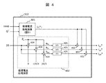
- FIG. 4 is a diagram showing a configuration example of the circulating current command calculation means 312 according to the first embodiment of the present invention.
- the circulation current command calculation means 312 of FIG. 4 is composed of a circulation current amplitude calculation means 401, a circulation current phase calculation means 402, and a multiplier 403.
- FIG. 5 is an input / output characteristic diagram of the circulating current amplitude calculating means 401 according to the first embodiment of the present invention.
- the horizontal axis represents the power factor cos [phi
- the vertical axis represents the circulating current command I zu *, I zv *, I zw * current amplitude
- the power factor COS ⁇ calculated by the equation (6) cannot determine the inductive and capacitive properties of the reactive power Q'. Therefore, the circulating current amplitude calculation means 401 determines the inductive and capacitive properties by the sign of Q'with the reactive power Q'as an input.
- the circulating current amplitude calculation means 401 has an input / output characteristic in which the current amplitude
- the horizontal axis represents time, and the vertical axis represents the value of each voltage expressed in arbitrary units.
- Capacitor voltage V CUP_1 are voltage variation around the voltage command value V C. For DSMMC converter large, the voltage variation because a large current flows in each unit converter is increased, there is a period in which the deviation becomes large between the voltage command value V C.
- the output voltage command V UP * is a voltage command value calculated by the control device so that the desired arm current I UP flows.
- the time and the capacitor voltage V CUP_1 becomes bottom value the time the output voltage command V UP * reaches a peak value approximately matches.
- the maximum output voltage of the power converter 102 also drops. That is, at the moment when the bottom value of the capacitor voltage V CUP_1 and the peak value of the output voltage command V UP * overlap, the overmodulated operation mode in which the output voltage command V UP * becomes larger than the maximum output voltage of the power converter 102 is set. There is a risk of becoming.
- FIGS. 6, 7, and 8 have been described by taking the capacitor voltage V CUP_1 of the U-phase first unit converter and the U-phase output voltage command V UP * as examples, other unit converters and The same explanation can be made for other phases.
- the circulating current phases ⁇ ZU , ⁇ ZV , and ⁇ ZW in FIG. 4 are calculated by the following equations (7) to (9).
- ⁇ ZU 2 ⁇ + ⁇ c (7)
- ⁇ ZV 2 ⁇ + ⁇ c + (2 ⁇ / 3)
- ⁇ ZW 2 ⁇ + ⁇ c + (-2 ⁇ / 3)
- ⁇ c is a phase compensation element.
- the phase order is a secondary harmonic, it is a reverse phase of U ⁇ W ⁇ V.
- the case where the voltage phase ⁇ of the output AC voltage is doubled will be described as an example, but the present invention is not limited to this, and the case is larger than the voltage phase ⁇ of the output AC voltage ( For example, 4 ⁇ , 6 ⁇ , etc.) and the phase order according to the order can obtain the same effect.
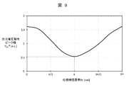
- FIG. 9 is a diagram showing the relationship between the phase compensation element ⁇ c and the peak value of the output voltage command V UP *.
- the horizontal axis represents the phase compensation element ⁇ c, and the vertical axis represents the peak value of the output voltage command V UP * expressed in arbitrary units. From FIG. 9, in order to effectively reduce the peak value of the output voltage command V UP * , the phase compensation element ⁇ c may be set to ⁇ (rad).
- the circulating current phase calculating means 402 resulting circulating current command from I zu *, I zv *, I zw * current amplitude and circulating current phase phi ZU, phi Circulating current commands I zu * , I zv * , and I zw * are generated by multiplying a sinusoidal signal having ZV and ⁇ ZW with the multiplier 403. That is, the circulating current commands I zu * , I zv * , and I zw * are changed from the following equations (10) to (12).
- the circulating current control means 313 adjusts the difference between the circulating current commands I zu * , I zv * , and I zw * and the circulating currents I zu , I zv , and I zw * derived by the arm current separating means 301.
- the circulating voltage target values V zu * , V zv * , and V zw * are generated.
- the PWM command generation means 306 of the P-side arm converter and the PWM command generation means 307 of the N-side arm converter have the three-phase output AC voltage set values generated by the AC current control means 302.
- Addition signals of V U * , V V * , V W * and circulating voltage target values V zu * , V zv * , V zw * generated by the circulating current control means 304 (V Up * , V Vp * for 306).
- V Wp * , 307, V UN * , V VN * , V WN * are applied as voltage target signals, respectively.
- the PWM command generation means 306 of the P-side arm converter and the PWM command generation means 307 of the N-side arm converter give each of the positive and negative arms and each unit converter 200 in each arm. Generates a gate signal and controls it.
- the output of the circulating current control means 304 is reflected in the output of the AC current control means 302 to obtain the target signals of the PWM command generation means 306 and 307 of the PN side arm converter. It is a thing. As a result, the circulating current is controlled according to the power factor.
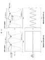
- FIG. 10 and 11 show examples of operation waveforms of each part before and after applying the circulating current command calculation means 312 of the present invention.
- the left side of FIG. 10 is before the circulation current command calculation means 312 is applied, and the right side of FIG. 10 is after the circulation current command calculation means 312 is applied.
- the upper left and right are the capacitor voltage V CUP_1 and the output voltage command V UP *
- the lower left and right are the circulating current command I zu * .
- the bottom value of the capacitor voltage V CUP_1 and the peak value of the output voltage command V UP * generally match.
- the voltage fluctuation of the capacitor voltage V CUP_1 is reduced by passing the circulating current shown in this embodiment, and the output voltage command V UP *.
- the peak value of can be prevented from overlapping the bottom value of the capacitor voltage V CUP_1.
- the peak value of the output voltage command VUP * can be reduced by the circulating current shown in the present invention.
- the left side of FIG. 11 is before the circulation current command calculation means 312 is applied, and the right side of FIG. 11 is after the circulation current command calculation means 312 is applied.
- the upper left and right of FIG. 11 are the capacitor voltage V CUP_1 and the output voltage command V UP *
- the lower left and right of FIG. 11 are the circulating current command I zu * .
- a voltage command value V C of the capacitor voltage V CUP_1, the output voltage command V UP * peak values are substantially coincident.
- the value of the capacitor voltage V CUP_1 is set to the command value V at the peak of the output voltage command V UP * by passing the circulating current shown in this embodiment. It can be shifted above C. That is, in the right side of FIG. 11, the peak value of the output voltage command V UP * can be reduced by applying the circulating current command calculation means 312.
- FIG. 12 is a diagram showing a configuration example of the power conversion device according to the second embodiment of the present invention. Since the figure numbers overlapping with FIG. 1 have the same meaning, the description thereof will be omitted, but the control device side has been changed while the main circuit configuration remains the same.
- FIG. 12 shows that the power factor command COS ⁇ * sent from the upper control device 1201 to the control device 108 is input to the control device 108 as compared with FIG. 1 of the first embodiment, and the power factor command COS ⁇ from the upper control device 1201 is shown. The difference is that it is provided with an interface for sending * to the control device 108.
- FIG. 13 Another configuration example of the power conversion device according to the second embodiment of FIG. 13 is a point that the AC current detector 1301 and the power factor detector 1302 are newly provided as compared with FIG. 1 of the first embodiment, and the power factor detector. The difference is that it is provided with an interface for sending the power factor COS ⁇ detected by 1302 to the control device 108.
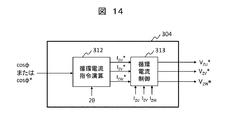
- FIG. 14 is a diagram showing a configuration example of the circulating current command calculation means according to the second embodiment of the present invention.
- the PQ calculation means 309, the filter circuit 310, and the power factor calculation means 311 in the circulating current control means 304 are unnecessary. It is characterized by points.
- FIG. 15 is a diagram showing a configuration example of the circulating current command calculation means according to the third embodiment of the present invention. Since the figure numbers overlapping with FIG. 4 have the same meaning, the description thereof will be omitted.
- the circulating current command calculation means 312 of FIG. 15 is different from FIG. 4 of the first embodiment in that it includes the time constant calculation means 1501. Further, the circulating current amplitude calculation means 1502 is different.
- the time constant calculation means 1501 calculates the time constant ⁇ by inputting the active power P', the number N of unit converters per arm converter, the voltage command value VC of the capacitor voltage, and the capacitance C of the capacitor.
- the circulating current amplitude calculation means 1502 will be described with reference to FIG.
- FIG. 16 is an input / output characteristic diagram of the circulating current amplitude calculating means according to the third embodiment of the present invention.
- the circulation current amplitude calculation means 1502 of the third embodiment is different from the first embodiment in that the circulation current amplitude can be selected according to the value of the time constant ⁇ .
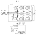
- FIG. 17 is a circuit diagram showing another configuration example of the circulating current amplitude calculating means according to the third embodiment of the present invention.
- FIG. 17 is different from FIG. 1 of the first embodiment in that it includes a storage device 1701 and an interface necessary for exchanging input / output signals between the storage device 1701 and the control device 108.
- the storage device 1701 is a device that stores and stores data such as a register, a flash memory, and a hard disk drive.
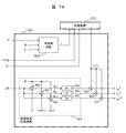
- FIG. 18 is a storage device according to a third embodiment of the present invention. Further, FIG. 19 is a block diagram of the circulating current command calculation means according to the third embodiment of the present invention.
- the storage device 1701 has a database 1801 inside, and selects from the database 1801 the circulating current amplitude
- the circulating current amplitude can be automatically adjusted according to the change of the time constant ⁇ , so that the optimum circulating current can be selected for each operating condition.
- Equipment can be provided.
- 101 Power system
- 102 Power converter
- 103 Variable DC voltage source
- 104 Transformer
- 105UP, 105UN, 105VP, 105VN, 105WP, 105WN Arm converter
- 106UP, 106UN, 106VP, 106VN, 106WP, 106WN Circulating current suppression reactor
- 108 Control device
- 109 AC voltage detector
- 203 Switching circuit
- 204 Condenser
- 205 DC voltage detector
- 206 Cell control device
- 207 Gate drive circuit
- 301 Arm current separation means
- 302 AC current control means
- 303 DC current control means
- 304 Circulating current control means
- 305 Phase Detection means
- 306 PWM command generation means
- 308 Coordinate conversion means
- 309 PQ calculation means
- 310 Filter circuit, 3
Landscapes
- Engineering & Computer Science (AREA)
- Power Engineering (AREA)
- Inverter Devices (AREA)
Abstract
高効率な電力変換装置の制御装置及び制御方法を提供する。エネルギー蓄積要素を備える単位変換器を複数直列接続したアーム変換器を交流の1相あたり1つ以上備えるモジュラーマルチレベル形の電力変換装置の制御装置であって、電力変換装置の制御装置は、交流電流を所望の値にフィードバック制御する交流電流制御手段と、モジュラーマルチレベル形の電力変換装置の交流の各相のアーム変換器を流れる循環電流を循環電流指令値にフィードバック制御する循環電流制御手段と、交流電流制御手段の出力を循環電流制御手段の出力で補正して得た交流各相の交流電圧目標に従って、アーム変換器を構成する単位変換器のゲート信号を生成し、制御するPWM指令生成手段を備え、循環電流制御手段は、電力変換装置の力率に応じて循環電流指令値の振幅を演算する循環電流指令演算手段を備えることを特徴とする電力変換装置の制御装置。
Description
本発明は、モジュラー・マルチレベル変換器(以下、MMC変換器と略称する)で構成した電力変換装置の制御装置及び制御方法に関する。
MMC変換器は、エネルギー蓄積要素であるコンデンサ等の電圧源と、ハーフブリッジ回路で構成される単位変換器を複数直列に接続することで構成する。単位変換器は、ハーフブリッジ回路のPWM変調率を制御することで所望の電圧を発生する。この単位変換器を複数直列接続して2端子のアーム変換器を構成し、このアーム変換器の第1の端子を交流電源の各相端子に接続し、星型結線した第2の端子を直流電源の端子に接続する。
このように各相に接続されたアーム変換器は、所望の交流電圧を発生して交流電流制御すると同時に、直流電流を重畳して直流電源との間で電力変換を実現する。
MMC変換器の制御は、外部からの交流電流指令と直流電流指令にアーム変換器に流れるアーム電流を調整する電流制御、アーム変換器内のコンデンサの合計蓄積エネルギーをアーム変換器間で平衡に保つための循環電流を調整する機能(以下、循環電流制御と称す)、単位変換器に設けたハーフブリッジ回路のPWM変調率をアーム内で相互に調整することでコンデンサの平均電圧を単位変換器間で平衡に保つ機能(以下、段間バランス制御と称す)を備える。このうち、循環電流制御を実現するには、アーム変換器間に流れる循環電流を抑制する為の回路素子が必要となる。
特許文献1は、MMC変換器の一形態であるダブルスター形MMC変換器(以下、DSMMC変換器と略称する)が開示されている。特許文献1によれば、各アーム変換器の第1の端子と交流電源端子の間にインダクタンスを設けることでアーム変換器間に流れる循環電流を抑制できることが開示されている。また、アーム変換器内のコンデンサの合計蓄積エネルギーをアーム変換器間でバランスさせる目的で、二次調波の循環電流を用いることが開示されている。本発明は、特許文献1に開示されているようなDSMMC変換器で構成する電力変換装置の制御手法を対象とする。
単位変換器内のコンデンサは、DSMMC変換器の出力交流周波数により決まる周期で充放電を繰り返すことで電圧変動する。例えば、直流送電設備や周波数変換設備に用いる大容量のDSMMC変換器の場合は、各単位変換器に大電流が流れることでコンデンサ電圧変動が大きくなる。その場合、電圧変動のピーク電圧値が高くなることからコンデンサの電圧定格を大きくする必要がありDSMMC変換器が大型化する課題がある。
前記の課題に対して、例えば特許文献2によれば、DSMMC変換器において、交流系統の系統周波数の偶数倍の周波数成分を含む循環電流をアーム変換器に流すことでコンデンサ電圧変動を抑制できることが開示されている。
循環電流は、交流電源にも直流電源にも流れずにアーム変換器内部を循環する電流である。電力変換装置の役割は、異なる複数の電源間の電力変換を実現することにある。したがって、高効率な電力変換装置を実現するには、循環電流を必要最小限にできることが望ましい。
この点に関し、特許文献1は、この循環電流に関する具体的な決定手段が開示されていない。特許文献2は、交流電流指令値から二次調波の循環電流指令値を生成することでコンデンサの電圧変動量を減少させる手段を開示している。一方、電力変換装置は出力交流電圧と交流電流の位相差により所望の交流電力を発生させるので、DSMMC変換器のコンデンサ電圧変動波形は電力変換装置の力率により変化する。従って、力率を考慮したうえで必要な循環電流を生成することが高効率な電力変換装置を実現するために望ましいが、特許文献2は、そのような手段を備えていない課題が残っている。
以上のことから本発明の目的は、上記の課題を解決し高効率な電力変換装置の制御装置及び制御方法を提供することにある。
以上のことから本発明においては、「エネルギー蓄積要素を備える単位変換器を複数直列接続したアーム変換器を交流の1相あたり1つ以上備えるモジュラーマルチレベル形の電力変換装置の制御装置であって、電力変換装置の制御装置は、交流電流を所望の値にフィードバック制御する交流電流制御手段と、モジュラーマルチレベル形の電力変換装置の交流の各相のアーム変換器を流れる循環電流を循環電流指令値にフィードバック制御する循環電流制御手段と、交流電流制御手段の出力を循環電流制御手段の出力で補正して得た交流各相の交流電圧目標に従って、アーム変換器を構成する単位変換器のゲート信号を生成し、制御するPWM指令生成手段を備え、循環電流制御手段は、電力変換装置の力率に応じて循環電流指令値の振幅を演算する循環電流指令演算手段を備えることを特徴とする電力変換装置の制御装置。」としたものである。
また本発明においては、「エネルギー蓄積要素を備える単位変換器を複数直列接続したアーム変換器を交流の1相あたり1つ以上備えるモジュラーマルチレベル形の電力変換装置の制御方法であって、交流電流を所望の値にフィードバック制御する交流電流制御出力を、モジュラーマルチレベル形の電力変換装置の交流の各相のアーム変換器を流れる循環電流を循環電流指令値にフィードバック制御する循環電流制御出力で補正して得た交流各相の交流電圧目標に従って、アーム変換器を構成する単位変換器のゲート信号を生成し、制御するとともに、電力変換装置の力率に応じて循環電流指令値の振幅を定めることを特徴とする電力変換装置の制御方法。」としたものである。
本発明によれば、力率を考慮したうえで必要な循環電流を生成するので高効率な電力変換装置の制御装置及び方法を提供できる。
以下、本発明に係る電力変換装置の制御装置及び方法の実施例を図面に基づいて説明する。なお、実施例により本発明が限定されるものではない。
図1は、本発明が適用可能な一般的な電力変換装置の構成例を示す図である。
図1において、電力変換装置102は、変圧器104を介して交流電力系統101に連系する。電力変換装置102は、可変直流電圧源103と接続する。このように構成することで、交流電力系統101と可変直流電圧源103間の電力融通を実現できる。電力変換装置102は、DSMMC変換器で構成する。
電力変換装置102は、アーム変換器105とリアクトル106が直列接続された6組のアームが、いわゆるグレーツ結線されて構成されている。具体的には電力変換装置102は、a端子とb端子の2つの出力端子を備えた6つのアーム変換器105(105UP、105UN、105VP、105VN、105WP、105WN)と、6つの循環電流抑制リアクトル106(106UP、106UN、106VP、106VN、106WP、106WN)により基本的に構成されており、さらに制御用の信号入手のために、各相のアーム電流I(IUP、IUN、IVP、IVN、IWP、IWN)を検出するための6つの電流検出器107(107UP、107UN、107VP、107VN、107WP、107WN)を備えている。
制御装置108は、6つの電流検出器107からのアーム電流と、交流電圧検出器109からの電力変換装置102の出力交流電圧VG(VGU、VGV、VGW)を検出して入力し、6つのアーム変換器105に対するゲート制御信号gを与える。なお、本発明の説明において交流の各相をU、V、Wで表し、直流回路の正負を夫々PNとする記号を付与して説明するものとする。また図1以降の各図において、各種の信号線に3、6、3Nと表記しているのは、1本で記述された信号線の総本数を示している。
図1の電力変換部において、正側のアーム変換器105UP、105VP、105WPのb端子、および、負側のアーム変換器105UN、105VN、105WNのa端子は、循環電流抑制リアクトル106(106UP、106UN、106VP、106VN、106WP、106WN)を介して交流電源端子(U端子、V端子、W端子)と接続する。正側のアーム変換器105UP、105VP、105WPのa端子、および、負側のアーム変換器105UN、105VN、105WNのb端子は、直流の正負の端子(P端子、N端子)と接続する。可変直流電圧源103についても前記の直流端子に接続する。
図2は、本発明が適用可能な一般的なアーム変換器の構成例を示す図である。以降では、代表してアーム変換器105UPを説明するが、その他のアーム変換器105UN、105VP、105VN、105WP、105WNも同様の構成であるため、他のアーム変換器については説明を省略する。
アーム変換器105UPは、単位変換器200(200_1から200_N)をN個直列接続した回路である。単位変換器200は、ハーフブリッジ回路を用いた場合であり、Nはアーム変換器あたりの単位変換器の個数である。単位変換器200は、環流ダイオードが並列接続されたスイッチング素子201、202を2つ直列接続したスイッチング回路203と、エネルギー蓄積要素であるコンデンサ204と、電圧検出器205をそれぞれ並列接続する。また、セル制御装置206と2つのゲート駆動回路207を備える。図2のa端子とb端子は、アーム変換器105UPの出力端子であり、図1のアーム変換器のa端子、b端子と対応する。
電圧検出器205は、各単位変換器のコンデンサ電圧を検出し、検出したコンデンサ電圧VC(VCUP_1からVCUP_N)をそれぞれの単位変換器200のセル制御装置206へ伝送する。
セル制御装置206は、図1の制御装置108から送り出される単位変換器のゲート指令g(gUP_1からgUP_N)をゲート駆動回路207に分配する。また、電圧検出器205が検出したコンデンサ電圧VCUP_1からVCUP_Nを制御装置108へ送り出す。
ゲート駆動回路207は、ゲート指令gに応じて、スイッチング素子201、202のオン、オフを切り替えるゲート駆動信号を生成し、各スイッチング素子201、202に与える。
図3は、本発明の実施例1に係る制御装置の構成例を示す図である。制御装置108は、アーム電流I(IUP、IUN、IVP、IVN、IWP、IWN)と、6×N個全ての単位変換器のコンデンサ電圧VC(VCUP_1からVCUP_N、VCUN_1からVCUN_N、VCVP_1からVCVP_N、VCVN_1からVCVN_N、VCWP_1からVCWP_N、VCWN_1からVCWN_N)と、出力交流電圧VG(VG
U、VGV、VGW)を入力として、各単位変換器に与える6×N個のゲート指令g(gUP_1からgUP_N、gUN_1からgUN_N、gVP_1からgVP_N、gVN_1からgVN_N、gWP_1からgWP_N、gWN_1からgWN_N)を出力
する。
U、VGV、VGW)を入力として、各単位変換器に与える6×N個のゲート指令g(gUP_1からgUP_N、gUN_1からgUN_N、gVP_1からgVP_N、gVN_1からgVN_N、gWP_1からgWP_N、gWN_1からgWN_N)を出力
する。
制御装置108は、アーム電流分離手段301、交流電流制御手段302、直流電流制御手段303、循環電流制御手段304、位相検出手段305、P側アーム変換器のPWM指令生成手段306、N側アーム変換器のPWM指令生成手段307、座標変換手段308から構成される。
この制御装置108の構成において本発明は、交流電流制御手段302の出力に循環電流制御手段304の出力を反映させて、PN側アーム変換器のPWM指令生成手段(PWM&段間バランス制御)306、307の目標信号としたものである。そしてそれ以外の手段301、303、305、308、は、本発明で実行する処理において使用する信号を生成するものであり、これらの内部処理は、特許文献1や特許文献2に記載されて公知のものであるので、ここでは概略のみを説明するに留める。
アーム電流分離手段301は、アーム電流I(IUP、IUN、IVP、IVN、IWP、IWN)を入力して、交流電流Iu、Iv、Iwと、変換器の上下アーム間を循環する循環電流Izu、Izv、Izwと、直流電流IDCを生成する。この中で循環電流制御手段304で使用する循環電流Izu、Izv、Izwは、以下の(1)(2)(3)式により求めることができる。
[数1]
Izu=(IUP+IUN)/2-IDC/3 (1)
[数2]
Izv=(IVP+IVN)/2-IDC/3 (2)
[数3]
Izw=(IWP+IWN)/2-IDC/3 (3)
直流電流制御手段303は、直流電流IDCとその目標電流IDC *を入力して、直流電圧目標値VDC *を生成する。位相検出手段305は、出力交流電圧VG(VGU、VGV、VGW)を入力して、位相θ、2θを生成する。座標変換手段308は、3相の出力交流電圧VG(VGU、VGV、VGW)を入力して直交の2軸座標電圧Vα、Vβに変換し、3相の循環電流Izu、Izv、Izwを入力して直交の2軸座標電流Iα、Iβに変換する。
[数1]
Izu=(IUP+IUN)/2-IDC/3 (1)
[数2]
Izv=(IVP+IVN)/2-IDC/3 (2)
[数3]
Izw=(IWP+IWN)/2-IDC/3 (3)
直流電流制御手段303は、直流電流IDCとその目標電流IDC *を入力して、直流電圧目標値VDC *を生成する。位相検出手段305は、出力交流電圧VG(VGU、VGV、VGW)を入力して、位相θ、2θを生成する。座標変換手段308は、3相の出力交流電圧VG(VGU、VGV、VGW)を入力して直交の2軸座標電圧Vα、Vβに変換し、3相の循環電流Izu、Izv、Izwを入力して直交の2軸座標電流Iα、Iβに変換する。
交流電流制御手段302は、位相角θを用いて3相の交流電流Iu、Iv、Iwを2軸電流Iα、Iβに座標変換し、予め設定されている2軸電流の目標値Iα
*、Iβ
*との差分を、それぞれ電流調節器を介して演算し、さらに2軸から3軸への逆座標変換により、3相の出力交流電圧設定値VG
*(VGU
*、VGV
*、VGW
*)を生成し、出力する。
本発明の主要回路部分である循環電流制御手段304は、PQ演算手段309、フィルタ回路310、力率演算手段311、循環電流指令演算手段312、循環電流制御手段313から構成される。
このうちPQ演算手段309は、座標変換手段308から得られる出力交流電圧Vα、Vβと交流電流Iα、Iβから電力変換装置102の出力する有効電力P、無効電力Qを演算する手段である。有効電力P、無効電力Qは、以下の(4)式、(5)式で演算する。
[数4]
P=Vα×Iα+Vβ×Iβ (4)
[数5]
Q=Vα×Iβ-Vβ×Iα (5)
フィルタ回路310は、有効電力P、無効電力Qに含まれる高周波成分を除去する。力率演算手段311は、フィルタ回路310から得られる高周波成分が除かれた有効電力P’、無効電力Q’から力率COSφを演算する。力率COSφは、以下の(6)で演算する。
[数6]
COSφ=P’/{(P’2+Q’2)1/2} (6)
循環電流指令演算手段312は、力率COSφを入力として各相の循環電流指令Izu *、Izv *、Izw *を演算する手段である。なお、具体的な循環電流指令Izu *、Izv *、Izw *の演算方法は後述する。
[数4]
P=Vα×Iα+Vβ×Iβ (4)
[数5]
Q=Vα×Iβ-Vβ×Iα (5)
フィルタ回路310は、有効電力P、無効電力Qに含まれる高周波成分を除去する。力率演算手段311は、フィルタ回路310から得られる高周波成分が除かれた有効電力P’、無効電力Q’から力率COSφを演算する。力率COSφは、以下の(6)で演算する。
[数6]
COSφ=P’/{(P’2+Q’2)1/2} (6)
循環電流指令演算手段312は、力率COSφを入力として各相の循環電流指令Izu *、Izv *、Izw *を演算する手段である。なお、具体的な循環電流指令Izu *、Izv *、Izw *の演算方法は後述する。
循環電流制御手段313は、各相の循環電流Izu、Izv、Izwを循環電流指令Izu
*、Izv
*、Izw
*に追従させる手段である。循環電流制御手段313は、比例制御器や比例積分制御器で構成して指令値に各相の循環電流が追従するような循環電圧指令値VZU
*、VZV
*、VZW
*を生成する。
図4から図9を用いて循環電流指令Izu
*、Izv
*、Izw
*の演算方法を説明する。まず図4は、本発明の実施例1に係る循環電流指令演算手段312の構成例を示す図である。図4の循環電流指令演算手段312は、循環電流振幅演算手段401、循環電流位相演算手段402、乗算器403から構成される。
まず、循環電流振幅演算手段401の演算方法について図5を用いて説明する。図5は、本発明の実施例1に係る循環電流振幅演算手段401の入出力特性図である。横軸は力率COSφを表し、縦軸は循環電流指令Izu
*、Izv
*、Izw
*の電流振幅|Iz
*|を表す。ここで、(6)式により演算する力率COSφは、無効電力Q’の誘導性、容量性を判別できない。そのため、循環電流振幅演算手段401は、無効電力Q’も入力としてQ’の符号により誘導性、容量性を判別する。
循環電流振幅演算手段401は、COSφ=0(誘導性)のときの電流振幅|Izmax
*|をピーク値として、力率1まで線形に減少する入出力特性を有する。また、COSφ=1からCOSφ=0(容量性)のときは、電流振幅|Izmin
*|が一定の入出力特性を有する。つまり、COSφ=0(誘導性)の期間のみ循環電流を増加させるように演算し、COSφ=1からCOSφ=0(容量性)の期間は、コンデンサの電圧バランスを保つための最小限の循環電流を流すようにする。このようにする理由を図6から図8を用いて説明する。
図6は、COSφ=0(誘導性)のときのコンデンサ電圧VCUP_1と出力電圧指令VUP
*の関係を示す図である。横軸は時間を表し、縦軸は任意単位で表した各電圧の値である。コンデンサ電圧VCUP_1は電圧指令値VCを中心に電圧変動している。大容量のDSMMC変換器の場合は、各単位変換器に大電流が流れるため電圧変動が大きくなり、電圧指令値VCとの偏差が大きくなる期間がある。出力電圧指令VUP
*は、所望のアーム電流IUPが流れるように制御装置で演算された電圧指令値である。
図6は、コンデンサ電圧VCUP_1がボトム値となる時間と、出力電圧指令VUP
*がピーク値となる時間が概ね一致する。コンデンサ電圧VCUP_1が電圧指令値VUP
*から低下すると、電力変換装置102の出力可能な最大電圧も低下する。つまり、コンデンサ電圧VCUP_1のボトム値と出力電圧指令VUP
*のピーク値が重なる瞬間は、電力変換装置102の出力可能な最大電圧よりも出力電圧指令VUP
*が大きくなる過変調運転モードになるおそれがある。
過変調運転を続けると電力変換装置102の交流電流波形が大きく歪み、高調波を増大させることで電力変換装置102の連系する電力系統101の電力品質を低下させるおそれがある。従って、コンデンサ電圧VCUP_1のボトム値と出力電圧指令VUP
*のピーク値が重ならないようにする手段が必要であり、本実施例では循環電流を用いてこの課題を解決する。
図7は、COSφ=1のときのコンデンサ電圧VCUP_1出力電圧指令VUP
*の関係を示す図である。コンデンサ電圧VCUP_1は電圧指令値VCを中心に電圧変動している。コンデンサ電圧VCUP_1のボトム値と出力電圧指令VUP
*のピーク値が重ならないことから、COSφ=1の場合は、図6のCOSφ=0(誘導性)の場合と比較して過変調運転となる可能性は低い。そのため、コンデンサの電圧バランスを保つための最小限の循環電流でよい。
図8は、COSφ=0(容量性)のときのコンデンサ電圧VCUP_1と出力電圧指令VUP
*の関係を示す図である。コンデンサ電圧VCUP_1は電圧指令値VCを中心に電圧変動している。コンデンサ電圧VCUP_1のボトム値と出力電圧指令VUP
*のピーク値が重ならないことから、COSφ=0(容量性)の場合はCOSφ=0(誘導性)の場合と比較して過変調運転となる可能性は低い。そのため、コンデンサの電圧バランスを保つための最小限の循環電流でよい。
以上、図6、図7、図8の結果から、過変調運転を防止するために必要な循環電流は、COSφ=0(誘導性)の場合をピーク値としてCOSφ=1まで線形に減少するように循環電流振幅演算手段401を構成する。また、COSφ=1からCOSφ=0(容量性)のときは、コンデンサの電圧バランスを保つための最小限の循環電流を流すように循環電流振幅演算手段401を構成する。つまり、無効電力が容量性の場合は、循環電流を少なくすることができるので、同一の皮相電力で誘導性の無効電力を出力する場合に比べて変換器効率を高くすることができる。なお、図6、図7、図8はU相の第1単位変換器のコンデンサ電圧VCUP_1とU相の出力電圧指令VUP
*を例に説明したが、他の単位変換器の場合や、他相の場合も同様の説明が可能である。
次に、循環電流位相演算手段402を説明する。図4の循環電流位相φZU、φZV、φZWは、以下の(7)式から(9)式で演算する。
[数7]
φZU=2θ+φc (7)
[数8]
φZV=2θ+φc+(2π/3) (8)
[数9]
φZW=2θ+φc+(-2π/3) (9)
ここで、φcは位相補償要素である。また、相順は二次調波であることからU→W→Vの逆相である。なお、本実施例は、出力交流電圧の電圧位相θを2倍した場合を例に説明するが、本発明はこれに限定されるものではなく、出力交流電圧の電圧位相θよりも大きい場合(例えば4θ、6θなど)かつ次数に応じた相順であれば同様の効果を得ることができる。
[数7]
φZU=2θ+φc (7)
[数8]
φZV=2θ+φc+(2π/3) (8)
[数9]
φZW=2θ+φc+(-2π/3) (9)
ここで、φcは位相補償要素である。また、相順は二次調波であることからU→W→Vの逆相である。なお、本実施例は、出力交流電圧の電圧位相θを2倍した場合を例に説明するが、本発明はこれに限定されるものではなく、出力交流電圧の電圧位相θよりも大きい場合(例えば4θ、6θなど)かつ次数に応じた相順であれば同様の効果を得ることができる。
位相補償要素φcの決定方法を、図9を用いて説明する。図9は、位相補償要素θcと出力電圧指令VUP
*のピーク値の関係を表した図である。横軸は位相補償要素θcを表し、縦軸は任意単位で表した出力電圧指令VUP
*のピーク値である。図9から、出力電圧指令VUP
*のピーク値を効果的に低減するには位相補償要素φcをπ(rad)とすればよい。
以上の循環電流振幅演算手段401と、循環電流位相演算手段402から得られる循環電流指令Izu
*、Izv
*、Izw
*の電流振幅|Iz
*|と、循環電流位相φZU、φZV、φZWを有する正弦波信号を乗算器403で乗算することで循環電流指令Izu
*、Izv
*、Izw
*を生成する。つまり、循環電流指令Izu
*、Izv
*、Izw
*は、以下の(10)式から(12)式となる。
[数10]
Izu *=|Iz *|×sin(φzu) (10)
[数11]
Izv *=|Iz *|×sin(φzv) (11)
[数12]
Izw *=|Iz *|×sin(φzw) (12)
図3に戻り、循環電流制御手段313は、循環電流指令Izu *、Izv *、Izw *とアーム電流分離手段301で導出した循環電流Izu、Izv、Izwの差分を調節器において比例積分処理した結果として循環電圧目標値Vzu *、Vzv *、Vzw *を生成する。
[数10]
Izu *=|Iz *|×sin(φzu) (10)
[数11]
Izv *=|Iz *|×sin(φzv) (11)
[数12]
Izw *=|Iz *|×sin(φzw) (12)
図3に戻り、循環電流制御手段313は、循環電流指令Izu *、Izv *、Izw *とアーム電流分離手段301で導出した循環電流Izu、Izv、Izwの差分を調節器において比例積分処理した結果として循環電圧目標値Vzu *、Vzv *、Vzw *を生成する。
さらに図3によれば、P側アーム変換器のPWM指令生成手段306と、N側アーム変換器のPWM指令生成手段307には、交流電流制御手段302で生成した3相の出力交流電圧設定値VU
*、VV
*、VW
*と、循環電流制御手段304で生成した循環電圧目標値Vzu
*、Vzv
*、Vzw
*の加算信号(306にはVUp
*、VVp
*、VWp
*、307にはVUN
*、VVN
*、VWN
*)が電圧目標信号として夫々印加される。これに応じて、P側アーム変換器のPWM指令生成手段306と、N側アーム変換器のPWM指令生成手段307では、正負の各アーム、かつ各アーム内の各単位変換器200に対して与えるゲート信号を生成し、これを制御する。
かくして上記構成を採用する本発明によれば、交流電流制御手段302の出力に循環電流制御手段304の出力を反映させて、PN側アーム変換器のPWM指令生成手段306、307の目標信号としたものである。これにより、力率に応じた循環電流に制御している。
図10、図11に本発明の循環電流指令演算手段312を適用する前後の各部動作波形例を示す。図10は、COSφ=0(誘導性)のときの動作波形例である。図10左は、循環電流指令演算手段312を適用する前、図10右は、循環電流指令演算手段312を適用した後である。また左右の上段は、コンデンサ電圧VCUP_1と出力電圧指令VUP
*で、左右の下段は、循環電流指令Izu
*である。
循環電流指令演算手段312を適用する前の図10左によれば、コンデンサ電圧VCUP_1のボトム値と、出力電圧指令VUP
*のピーク値が概ね一致している。一方、循環電流指令演算手段312を適用後の図10右によれば、本実施例で示した循環電流を流すことでコンデンサ電圧VCUP_1の電圧変動を小さくし、また、出力電圧指令VUP
*のピーク値がコンデンサ電圧VCUP_1のボトム値に重ならないようにすることができる。その結果、本発明で示した循環電流により出力電圧指令VUP
*のピーク値を低減できる。
図11は、COSφ=1のときの動作波形例である。図11左は、循環電流指令演算手段312を適用する前、図11右は、循環電流指令演算手段312を適用した後である。
図11左右の上段は、コンデンサ電圧VCUP_1と出力電圧指令VUP *で、図11左右の下段は、循環電流指令Izu *である。
図11左右の上段は、コンデンサ電圧VCUP_1と出力電圧指令VUP *で、図11左右の下段は、循環電流指令Izu *である。
循環電流指令演算手段312を適用する前の図11左によれば、コンデンサ電圧VCUP_1の電圧指令値VCと、出力電圧指令VUP
*のピーク値が概ね一致している。一方、循環電流指令演算手段312を適用後の図11右によれば、本実施例で示した循環電流を流すことで出力電圧指令VUP
*のピーク時にコンデンサ電圧VCUP_1の値を指令値VCよりも上にずらすことができる。つまり、図11右は、循環電流指令演算手段312を適用することで、出力電圧指令VUP
*のピーク値を低減することができる。なお、COSφ=1の循環電流指令値は、COSφ=0(誘導性)の場合よりも小さくてよく、コンデンサの電圧バランスを保つための最小限の循環電流を流すことができればよい。
以上で説明した動作により、力率に応じて循環電流を調整することで過変調運転を回避しつつ、循環電流を必要最小限に抑えることができるので高効率な電力変換装置を提供できる。
実施例2では、力率COSφの取り扱いについて図12から図14を用いて提案する。
まず図12は、本発明の実施例2に係る電力変換装置の構成例を示す図である。図1と重複する図番号は同じ意味であるので説明を省略するが、主回路構成はそのままに制御装置側が変更されている。図12は、実施例1の図1と比較して、上位制御装置1201から制御装置108に送り出される力率指令COSφ*を制御装置108の入力とする点、上位制御装置1201から力率指令COSφ*を制御装置108に送り出すためのインターフェースを備える点が異なる。
まず図12は、本発明の実施例2に係る電力変換装置の構成例を示す図である。図1と重複する図番号は同じ意味であるので説明を省略するが、主回路構成はそのままに制御装置側が変更されている。図12は、実施例1の図1と比較して、上位制御装置1201から制御装置108に送り出される力率指令COSφ*を制御装置108の入力とする点、上位制御装置1201から力率指令COSφ*を制御装置108に送り出すためのインターフェースを備える点が異なる。
図13の実施例2に係る電力変換装置の他の構成例は、実施例1の図1と比較して、交流電流検出器1301、力率検出器1302を新たに備える点、力率検出器1302で検出した力率COSφを制御装置108に送り出すためのインターフェースを備える点が異なる。
図14は、本発明の実施例2に係る循環電流指令演算手段の構成例を示す図である。ここでは、力率指令COSφ*、または、力率COSφの一方を制御装置108の入力とするため、循環電流制御手段304内のPQ演算手段309、フィルタ回路310、力率演算手段311が不要な点が特徴である。
本実施例によれば、制御装置内の演算手段を削減することで演算時間を削減できるのでより安価なマイコンを用いた電力変換装置を提供できる。
図15は、本発明の実施例3に係る循環電流指令演算手段の構成例を示す図である。図4と重複する図番号は同じ意味であるので説明を省略する。図15の循環電流指令演算手段312は、実施例1の図4と比較して、時定数演算手段1501を備える点が異なる。
また、循環電流振幅演算手段1502が異なる。
また、循環電流振幅演算手段1502が異なる。
まず、時定数演算手段1501は、有効電力P’、アーム変換器あたりの単位変換器の個数N、コンデンサ電圧の電圧指令値VC、コンデンサの静電容量Cを入力として時定数τを演算する。時定数τが長いほどコンデンサに同じ電流が流れた時の電圧変動が小さくなるので、必要な循環電流を小さくすることができる。時定数τは、以下の(13)式で演算する。この時定数τは、コンデンサの静電エネルギーを基準電力で放電させるために必要な時間と定義される。
[数13]
τ={(1/2)×C×VC2}/{P’/(6×N)} :(13)
次に、循環電流振幅演算手段1502について図16を用いて説明する。図16は、本発明の実施例3に係る循環電流振幅演算手段の入出力特性図である。実施例3の循環電流振幅演算手段1502は、実施例1と比較して時定数τの値に応じて循環電流振幅を選択できるようにした点が異なる。
[数13]
τ={(1/2)×C×VC2}/{P’/(6×N)} :(13)
次に、循環電流振幅演算手段1502について図16を用いて説明する。図16は、本発明の実施例3に係る循環電流振幅演算手段の入出力特性図である。実施例3の循環電流振幅演算手段1502は、実施例1と比較して時定数τの値に応じて循環電流振幅を選択できるようにした点が異なる。
図17は、本発明の実施例3に係る循環電流振幅演算手段の別の構成例を示す回路図である。図17は、実施例1の図1と比較して記憶装置1701を備える点、記憶装置1701と制御装置108間の入出力信号をやり取りするために必要なインターフェースを備える点が異なる。記憶装置1701は、例えばレジスタ、フラッシュメモリ、ハードディスクドライブ等のデータを保存、記憶する装置である。
図18は、本発明の実施例3に係る記憶装置である。また、図19は、本発明の実施例3に係る循環電流指令演算手段のブロック図である。記憶装置1701は、内部にデータベース1801を備え、制御装置108から送り出された力率COSφ、無効電力Q’、時定数τの3つの入力と一致する循環電流振幅|IZ*|をデータベース1801から選択して制御装置108内の循環電流指令演算手段312に送り出す。
本実施例によれば、電力変換装置の運転条件を変更した場合でも、時定数τの変化に従って循環電流振幅を自動調整することができるので、運転条件毎に最適な循環電流を選択できる電力変換装置を提供できる。
101:電力系統、102:電力変換装置、103:可変直流電圧源、104:変圧器、105UP、105UN、105VP、105VN、105WP、105WN:アーム変換器、106UP、106UN、106VP、106VN、106WP、106WN:循環電流抑制リアクトル、107UP、107UN、107VP、107VN、107WP、107WN:電流検出器、108:制御装置、109:交流電圧検出器、201、202:スイッチング素子、203:スイッチング回路、204:コンデンサ、205:直流電圧検出器、206:セル制御装置、207:ゲート駆動回路、301:アーム電流分離手段、302:交流電流制御手段、303:直流電流制御手段、304:循環電流制御手段、305:位相検出手段、306、307:PWM指令生成手段、308:座標変換手段、309:PQ演算手段、310:フィルタ回路、311:力率演算手段、312:循環電流指令演算手段、313:循環電流制御手段、401、1502:循環電流振幅演算手段、402:循環電流位相演算手段、403:乗算器、1201:上位制御装置、1301:交流電流検出器、1302:力率検出器、1501:時定数演算手段、1701:記憶装置、1801:データベース
Claims (12)
- エネルギー蓄積要素を備える単位変換器を複数直列接続したアーム変換器を交流の1相あたり1つ以上備えるモジュラーマルチレベル形の電力変換装置の制御装置であって、
電力変換装置の制御装置は、交流電流を所望の値にフィードバック制御する交流電流制御手段と、モジュラーマルチレベル形の電力変換装置の交流の各相のアーム変換器を流れる循環電流を循環電流指令値にフィードバック制御する循環電流制御手段と、前記交流電流制御手段の出力を前記循環電流制御手段の出力で補正して得た交流各相の交流電圧目標に従って、前記アーム変換器を構成する前記単位変換器のゲート信号を生成し、制御するPWM指令生成手段を備え、
前記循環電流制御手段は、電力変換装置の力率に応じて前記循環電流指令値の振幅を演算する循環電流指令演算手段を備えることを特徴とする電力変換装置の制御装置。 - 請求項1に記載の電力変換装置の制御装置であって、
前記循環電流指令値は、交流電圧の周波数より高次周波数の電流であることを特徴とする電力変換装置の制御装置。 - 請求項2に記載の電力変換装置の制御装置であって、
前記循環電流指令値の角周波数は、交流電源角周波数の二倍で回転する逆相電流であり、かつ、各相の交流電源電圧との位相差が180度であることを特徴とする電力変換装置の制御装置。 - 請求項1から請求項3のいずれか1項に記載の電力変換装置の制御装置であって、
前記循環電流指令値を単位変換器あたりの有効電力と前記エネルギー蓄積要素に蓄えられる静電エネルギーの比率によって決まる時定数に応じて、変更することを特徴とする電力変換装置の制御装置。 - 請求項1から請求項4のいずれか1項に記載の電力変換装置の制御装置であって、
電力変換装置は、記憶装置と記憶装置と制御装置間の信号を送受信するためのインターフェースを備え、前記記憶装置は、制御装置から送り出された力率、無効電力、時定数の3つの入力と一致する循環電流振幅を記憶装置内のデータベースから選択して制御装置内の循環電流指令演算手段に送り出すことで循環電流指令値を演算することを特徴とする電力変換装置の制御装置。 - 請求項1から請求項5のいずれか1項に記載の電力変換装置の制御装置であって、
外部の力率検出手段を用いて力率を検出し制御装置に取り込むインターフェースを備えることを特徴とする電力変換装置の制御装置。 - 請求項1から請求項6のいずれか1項に記載の電力変換装置の制御装置であって、
容量性無効電力を該電力変換装置から出力する場合は、循環電流を低減する方向に制御することで、同一皮相電力の誘導性無効電力を出力する場合に比べて変換器効率を高くする制御手段を備えることを特徴とする電力変換装置の制御装置。 - 請求項1から請求項7のいずれか1項に記載の電力変換装置の制御装置であって、
前記循環電流指令値の振幅は、容量性無効電力を電力変換装置から出力する場合は一定とされ、同一皮相電力の誘導性無効電力を電力変換装置から出力する場合は力率が低いほど大きな振幅とされることを特徴とする電力変換装置の制御装置。 - 請求項8に記載の電力変換装置の制御装置であって、
容量性無効電力を電力変換装置から出力する場合は一定とされる前記振幅は、同一皮相電力の誘導性無効電力を電力変換装置から出力する場合に力率が1であるときの振幅と同一とされることを特徴とする電力変換装置の制御装置。 - エネルギー蓄積要素を備える単位変換器を複数直列接続したアーム変換器を交流の1相あたり1つ以上備えるモジュラーマルチレベル形の電力変換装置の制御方法であって、
交流電流を所望の値にフィードバック制御する交流電流制御出力を、モジュラーマルチレベル形の電力変換装置の交流の各相のアーム変換器を流れる循環電流を循環電流指令値にフィードバック制御する循環電流制御出力で補正して得た交流各相の交流電圧目標に従って、前記アーム変換器を構成する前記単位変換器のゲート信号を生成し、制御するとともに、
電力変換装置の力率に応じて前記循環電流指令値の振幅を定めることを特徴とする電力変換装置の制御方法。 - 請求項10に記載の電力変換装置の制御方法であって、
前記循環電流指令値の振幅は、容量性無効電力を電力変換装置から出力する場合は一定とされ、同一皮相電力の誘導性無効電力を電力変換装置から出力する場合は力率が低いほど大きな振幅とされることを特徴とする電力変換装置の制御方法。 - 請求項11に記載の電力変換装置の制御方法であって、
容量性無効電力を電力変換装置から出力する場合は一定とされる前記振幅は、同一皮相電力の誘導性無効電力を電力変換装置から出力する場合に力率が1であるときの振幅と同一とされることを特徴とする電力変換装置の制御方法。
Priority Applications (1)
| Application Number | Priority Date | Filing Date | Title |
|---|---|---|---|
| EP21812217.4A EP4160901A4 (en) | 2020-05-25 | 2021-04-15 | CONTROL DEVICE AND CONTROL METHOD FOR A POWER CONVERSION DEVICE |
Applications Claiming Priority (2)
| Application Number | Priority Date | Filing Date | Title |
|---|---|---|---|
| JP2020-090327 | 2020-05-25 | ||
| JP2020090327A JP2021185727A (ja) | 2020-05-25 | 2020-05-25 | 電力変換装置の制御装置及び制御方法 |
Publications (1)
| Publication Number | Publication Date |
|---|---|
| WO2021241054A1 true WO2021241054A1 (ja) | 2021-12-02 |
Family
ID=78744300
Family Applications (1)
| Application Number | Title | Priority Date | Filing Date |
|---|---|---|---|
| PCT/JP2021/015556 Ceased WO2021241054A1 (ja) | 2020-05-25 | 2021-04-15 | 電力変換装置の制御装置及び制御方法 |
Country Status (3)
| Country | Link |
|---|---|
| EP (1) | EP4160901A4 (ja) |
| JP (1) | JP2021185727A (ja) |
| WO (1) | WO2021241054A1 (ja) |
Cited By (2)
| Publication number | Priority date | Publication date | Assignee | Title |
|---|---|---|---|---|
| CN116073422A (zh) * | 2022-10-26 | 2023-05-05 | 南方电网科学研究院有限责任公司 | 一种分布式直流耗能装置主回路参数设置方法及装置 |
| CN117833642A (zh) * | 2024-01-07 | 2024-04-05 | 国网江西省电力有限公司九江供电分公司 | 一种模块化多电dc/dc变换器控制方法 |
Families Citing this family (3)
| Publication number | Priority date | Publication date | Assignee | Title |
|---|---|---|---|---|
| WO2024134858A1 (ja) * | 2022-12-23 | 2024-06-27 | 三菱電機株式会社 | 電力変換装置 |
| WO2024150437A1 (ja) * | 2023-01-13 | 2024-07-18 | 日立三菱水力株式会社 | モジュラー・マルチレベル電力変換器 |
| EP4654456A1 (en) * | 2023-01-19 | 2025-11-26 | Hitachi Mitsubishi Hydro Corporation | Modular multi-level electric power converter |
Citations (7)
| Publication number | Priority date | Publication date | Assignee | Title |
|---|---|---|---|---|
| JP2005116191A (ja) * | 2003-10-02 | 2005-04-28 | Mitsui Eng & Shipbuild Co Ltd | 誘導加熱用並列インバータの給電方法および誘導加熱用並列型インバータ装置 |
| JP2010512133A (ja) * | 2006-12-08 | 2010-04-15 | シーメンス アクチエンゲゼルシヤフト | エネルギー蓄積器が配分されたモジュール式コンバータ |
| JP2012044839A (ja) * | 2010-08-23 | 2012-03-01 | Tokyo Institute Of Technology | 電力変換器 |
| JP2013251933A (ja) | 2012-05-30 | 2013-12-12 | Hitachi Ltd | 電圧型電力変換装置の制御装置及び制御方法 |
| KR20160072499A (ko) * | 2014-12-15 | 2016-06-23 | 엘에스산전 주식회사 | 모듈형 멀티 레벨 컨버터의 운전 방법 |
| JP6131030B2 (ja) * | 2012-03-21 | 2017-05-17 | 株式会社日立製作所 | 単位変換器、電力変換装置、直流送電システム、および、電力変換装置の制御方法 |
| JP2018196237A (ja) * | 2017-05-17 | 2018-12-06 | 株式会社東芝 | 電力変換装置 |
Family Cites Families (2)
| Publication number | Priority date | Publication date | Assignee | Title |
|---|---|---|---|---|
| JP5865104B2 (ja) * | 2012-02-09 | 2016-02-17 | 株式会社日立製作所 | 電圧型電力変換器の電流制御装置及び電圧型電力変換器の電流制御方法 |
| US9219426B2 (en) * | 2012-02-09 | 2015-12-22 | Hitachi, Ltd. | Switching element, power converter, direct current transmission system, current control device, method of controlling power converter, and method of controlling current in voltage source converter |
-
2020
- 2020-05-25 JP JP2020090327A patent/JP2021185727A/ja active Pending
-
2021
- 2021-04-15 WO PCT/JP2021/015556 patent/WO2021241054A1/ja not_active Ceased
- 2021-04-15 EP EP21812217.4A patent/EP4160901A4/en not_active Withdrawn
Patent Citations (7)
| Publication number | Priority date | Publication date | Assignee | Title |
|---|---|---|---|---|
| JP2005116191A (ja) * | 2003-10-02 | 2005-04-28 | Mitsui Eng & Shipbuild Co Ltd | 誘導加熱用並列インバータの給電方法および誘導加熱用並列型インバータ装置 |
| JP2010512133A (ja) * | 2006-12-08 | 2010-04-15 | シーメンス アクチエンゲゼルシヤフト | エネルギー蓄積器が配分されたモジュール式コンバータ |
| JP2012044839A (ja) * | 2010-08-23 | 2012-03-01 | Tokyo Institute Of Technology | 電力変換器 |
| JP6131030B2 (ja) * | 2012-03-21 | 2017-05-17 | 株式会社日立製作所 | 単位変換器、電力変換装置、直流送電システム、および、電力変換装置の制御方法 |
| JP2013251933A (ja) | 2012-05-30 | 2013-12-12 | Hitachi Ltd | 電圧型電力変換装置の制御装置及び制御方法 |
| KR20160072499A (ko) * | 2014-12-15 | 2016-06-23 | 엘에스산전 주식회사 | 모듈형 멀티 레벨 컨버터의 운전 방법 |
| JP2018196237A (ja) * | 2017-05-17 | 2018-12-06 | 株式会社東芝 | 電力変換装置 |
Non-Patent Citations (1)
| Title |
|---|
| See also references of EP4160901A4 |
Cited By (2)
| Publication number | Priority date | Publication date | Assignee | Title |
|---|---|---|---|---|
| CN116073422A (zh) * | 2022-10-26 | 2023-05-05 | 南方电网科学研究院有限责任公司 | 一种分布式直流耗能装置主回路参数设置方法及装置 |
| CN117833642A (zh) * | 2024-01-07 | 2024-04-05 | 国网江西省电力有限公司九江供电分公司 | 一种模块化多电dc/dc变换器控制方法 |
Also Published As
| Publication number | Publication date |
|---|---|
| EP4160901A4 (en) | 2024-07-10 |
| JP2021185727A (ja) | 2021-12-09 |
| EP4160901A1 (en) | 2023-04-05 |
Similar Documents
| Publication | Publication Date | Title |
|---|---|---|
| WO2021241054A1 (ja) | 電力変換装置の制御装置及び制御方法 | |
| US8154893B2 (en) | Three-phase power converting apparatus | |
| US6741482B2 (en) | Power conversion device | |
| CN105048788B (zh) | 一种混合级联结构的多端口电力电子变压器及其控制方法 | |
| US6594164B2 (en) | PWM controlled power conversion device | |
| JP6180641B2 (ja) | 電力変換装置 | |
| JP6752401B1 (ja) | 電力変換装置 | |
| CN112928898B (zh) | 功率变换器的bus电压均衡调节方法及功率变换器 | |
| CN117955167B (zh) | 构网型电压源变流器系统及多目标控制方法 | |
| CN115000978A (zh) | 一种h桥级联型statcom直流侧电压二倍频波动抑制方法 | |
| CN110829477A (zh) | 一种模块化多电平变换器子模块电容最小化优化方法 | |
| JP6818956B1 (ja) | 電力変換装置 | |
| JP2017118635A (ja) | 自励式無効電力補償装置 | |
| JP6771707B1 (ja) | 電力変換装置 | |
| CN105141159B (zh) | 一种三相模块化多电平逆变器并联系统及其控制方法 | |
| CN107947623A (zh) | 一种负载不平衡条件下双向ac/dc变换器的多模态自治运行控制方法 | |
| JP4365171B2 (ja) | 電力変換装置及びそれを用いたパワーコンディショナ | |
| CN111404412B (zh) | 一种模块化多电平变换器直流电容选取方法及装置 | |
| CN112104248A (zh) | 一种三电平npc变换器的控制方法 | |
| CN111817365B (zh) | 适用于超大规模储能的模块化多回路变流器控制方法 | |
| CN120262546B (zh) | 一种逆变器中点平衡与环流抑制协同控制方法 | |
| CN113131493A (zh) | 一种h桥级联型statcom直流侧电压二倍频波动抑制方法 | |
| CN116014753B (zh) | 电容电压均衡控制方法、装置及系统 | |
| CN120511735B (zh) | 用于抑制二次谐波电流的级联型储能变流器及控制方法 | |
| JP3311036B2 (ja) | 超電導エネルギー貯蔵装置 |
Legal Events
| Date | Code | Title | Description |
|---|---|---|---|
| 121 | Ep: the epo has been informed by wipo that ep was designated in this application |
Ref document number: 21812217 Country of ref document: EP Kind code of ref document: A1 |
|
| NENP | Non-entry into the national phase |
Ref country code: DE |
|
| ENP | Entry into the national phase |
Ref document number: 2021812217 Country of ref document: EP Effective date: 20230102 |