WO2021241541A1 - 樹脂組成物及び電子部品 - Google Patents
樹脂組成物及び電子部品 Download PDFInfo
- Publication number
- WO2021241541A1 WO2021241541A1 PCT/JP2021/019714 JP2021019714W WO2021241541A1 WO 2021241541 A1 WO2021241541 A1 WO 2021241541A1 JP 2021019714 W JP2021019714 W JP 2021019714W WO 2021241541 A1 WO2021241541 A1 WO 2021241541A1
- Authority
- WO
- WIPO (PCT)
- Prior art keywords
- resin composition
- less
- component
- resin
- mass
- Prior art date
- Legal status (The legal status is an assumption and is not a legal conclusion. Google has not performed a legal analysis and makes no representation as to the accuracy of the status listed.)
- Ceased
Links
Images

Classifications
-
- C—CHEMISTRY; METALLURGY
- C08—ORGANIC MACROMOLECULAR COMPOUNDS; THEIR PREPARATION OR CHEMICAL WORKING-UP; COMPOSITIONS BASED THEREON
- C08L—COMPOSITIONS OF MACROMOLECULAR COMPOUNDS
- C08L63/00—Compositions of epoxy resins; Compositions of derivatives of epoxy resins
- C08L63/08—Epoxidised polymerised polyenes
-
- H—ELECTRICITY
- H10—SEMICONDUCTOR DEVICES; ELECTRIC SOLID-STATE DEVICES NOT OTHERWISE PROVIDED FOR
- H10W—GENERIC PACKAGES, INTERCONNECTIONS, CONNECTORS OR OTHER CONSTRUCTIONAL DETAILS OF DEVICES COVERED BY CLASS H10
- H10W74/00—Encapsulations, e.g. protective coatings
- H10W74/40—Encapsulations, e.g. protective coatings characterised by their materials
- H10W74/47—Encapsulations, e.g. protective coatings characterised by their materials comprising organic materials, e.g. plastics or resins
- H10W74/473—Encapsulations, e.g. protective coatings characterised by their materials comprising organic materials, e.g. plastics or resins containing a filler
-
- C—CHEMISTRY; METALLURGY
- C08—ORGANIC MACROMOLECULAR COMPOUNDS; THEIR PREPARATION OR CHEMICAL WORKING-UP; COMPOSITIONS BASED THEREON
- C08K—Use of inorganic or non-macromolecular organic substances as compounding ingredients
- C08K3/00—Use of inorganic substances as compounding ingredients
- C08K3/02—Elements
- C08K3/04—Carbon
- C08K3/041—Carbon nanotubes
-
- C—CHEMISTRY; METALLURGY
- C08—ORGANIC MACROMOLECULAR COMPOUNDS; THEIR PREPARATION OR CHEMICAL WORKING-UP; COMPOSITIONS BASED THEREON
- C08K—Use of inorganic or non-macromolecular organic substances as compounding ingredients
- C08K3/00—Use of inorganic substances as compounding ingredients
- C08K3/02—Elements
- C08K3/04—Carbon
- C08K3/042—Graphene or derivatives, e.g. graphene oxides
-
- C—CHEMISTRY; METALLURGY
- C08—ORGANIC MACROMOLECULAR COMPOUNDS; THEIR PREPARATION OR CHEMICAL WORKING-UP; COMPOSITIONS BASED THEREON
- C08K—Use of inorganic or non-macromolecular organic substances as compounding ingredients
- C08K3/00—Use of inorganic substances as compounding ingredients
- C08K3/10—Metal compounds
- C08K3/14—Carbides
-
- C—CHEMISTRY; METALLURGY
- C08—ORGANIC MACROMOLECULAR COMPOUNDS; THEIR PREPARATION OR CHEMICAL WORKING-UP; COMPOSITIONS BASED THEREON
- C08K—Use of inorganic or non-macromolecular organic substances as compounding ingredients
- C08K3/00—Use of inorganic substances as compounding ingredients
- C08K3/34—Silicon-containing compounds
-
- C—CHEMISTRY; METALLURGY
- C08—ORGANIC MACROMOLECULAR COMPOUNDS; THEIR PREPARATION OR CHEMICAL WORKING-UP; COMPOSITIONS BASED THEREON
- C08L—COMPOSITIONS OF MACROMOLECULAR COMPOUNDS
- C08L63/00—Compositions of epoxy resins; Compositions of derivatives of epoxy resins
-
- H—ELECTRICITY
- H05—ELECTRIC TECHNIQUES NOT OTHERWISE PROVIDED FOR
- H05K—PRINTED CIRCUITS; CASINGS OR CONSTRUCTIONAL DETAILS OF ELECTRIC APPARATUS; MANUFACTURE OF ASSEMBLAGES OF ELECTRICAL COMPONENTS
- H05K9/00—Screening of apparatus or components against electric or magnetic fields
- H05K9/0073—Shielding materials
- H05K9/0075—Magnetic shielding materials
-
- H—ELECTRICITY
- H10—SEMICONDUCTOR DEVICES; ELECTRIC SOLID-STATE DEVICES NOT OTHERWISE PROVIDED FOR
- H10W—GENERIC PACKAGES, INTERCONNECTIONS, CONNECTORS OR OTHER CONSTRUCTIONAL DETAILS OF DEVICES COVERED BY CLASS H10
- H10W42/00—Arrangements for protection of devices
- H10W42/20—Arrangements for protection of devices protecting against electromagnetic or particle radiation, e.g. light, X-rays, gamma-rays or electrons
-
- H—ELECTRICITY
- H10—SEMICONDUCTOR DEVICES; ELECTRIC SOLID-STATE DEVICES NOT OTHERWISE PROVIDED FOR
- H10W—GENERIC PACKAGES, INTERCONNECTIONS, CONNECTORS OR OTHER CONSTRUCTIONAL DETAILS OF DEVICES COVERED BY CLASS H10
- H10W42/00—Arrangements for protection of devices
- H10W42/20—Arrangements for protection of devices protecting against electromagnetic or particle radiation, e.g. light, X-rays, gamma-rays or electrons
- H10W42/281—Arrangements for protection of devices protecting against electromagnetic or particle radiation, e.g. light, X-rays, gamma-rays or electrons characterised by their materials
- H10W42/284—Arrangements for protection of devices protecting against electromagnetic or particle radiation, e.g. light, X-rays, gamma-rays or electrons characterised by their materials shielding resins
-
- C—CHEMISTRY; METALLURGY
- C08—ORGANIC MACROMOLECULAR COMPOUNDS; THEIR PREPARATION OR CHEMICAL WORKING-UP; COMPOSITIONS BASED THEREON
- C08G—MACROMOLECULAR COMPOUNDS OBTAINED OTHERWISE THAN BY REACTIONS ONLY INVOLVING UNSATURATED CARBON-TO-CARBON BONDS
- C08G59/00—Polycondensates containing more than one epoxy group per molecule; Macromolecules obtained by polymerising compounds containing more than one epoxy group per molecule using curing agents or catalysts which react with the epoxy groups
- C08G59/18—Macromolecules obtained by polymerising compounds containing more than one epoxy group per molecule using curing agents or catalysts which react with the epoxy groups ; e.g. general methods of curing
- C08G59/20—Macromolecules obtained by polymerising compounds containing more than one epoxy group per molecule using curing agents or catalysts which react with the epoxy groups ; e.g. general methods of curing characterised by the epoxy compounds used
-
- C—CHEMISTRY; METALLURGY
- C08—ORGANIC MACROMOLECULAR COMPOUNDS; THEIR PREPARATION OR CHEMICAL WORKING-UP; COMPOSITIONS BASED THEREON
- C08K—Use of inorganic or non-macromolecular organic substances as compounding ingredients
- C08K2201/00—Specific properties of additives
- C08K2201/011—Nanostructured additives
-
- C—CHEMISTRY; METALLURGY
- C08—ORGANIC MACROMOLECULAR COMPOUNDS; THEIR PREPARATION OR CHEMICAL WORKING-UP; COMPOSITIONS BASED THEREON
- C08K—Use of inorganic or non-macromolecular organic substances as compounding ingredients
- C08K2201/00—Specific properties of additives
- C08K2201/014—Additives containing two or more different additives of the same subgroup in C08K
-
- C—CHEMISTRY; METALLURGY
- C08—ORGANIC MACROMOLECULAR COMPOUNDS; THEIR PREPARATION OR CHEMICAL WORKING-UP; COMPOSITIONS BASED THEREON
- C08L—COMPOSITIONS OF MACROMOLECULAR COMPOUNDS
- C08L2203/00—Applications
- C08L2203/20—Applications use in electrical or conductive gadgets
-
- H—ELECTRICITY
- H10—SEMICONDUCTOR DEVICES; ELECTRIC SOLID-STATE DEVICES NOT OTHERWISE PROVIDED FOR
- H10W—GENERIC PACKAGES, INTERCONNECTIONS, CONNECTORS OR OTHER CONSTRUCTIONAL DETAILS OF DEVICES COVERED BY CLASS H10
- H10W74/00—Encapsulations, e.g. protective coatings
- H10W74/10—Encapsulations, e.g. protective coatings characterised by their shape or disposition
- H10W74/111—Encapsulations, e.g. protective coatings characterised by their shape or disposition the semiconductor body being completely enclosed
Definitions
- the present disclosure relates to a resin composition and an electronic component having an electromagnetic wave absorbing function.
- ICs Integrated Circuits
- CPU Central Processing Unit
- PMIC Power Management Integrated Circuit
- Bluetooth registered trademark
- Patent Document 1 a sheet obtained by dispersing a soft magnetic metal powder such as a metal selected from Fe, Ni, Co and V or an alloy powder consisting of two or more of these metals in a rubber or plastic matrix.
- Patent Document 2 proposes a sheet-shaped radio wave absorber in which a radio wave absorbing layer formed of a radio wave absorbing material obtained by dispersing silicon carbide powder in a matrix resin is laminated on the surface of a metal body.
- Patent Document 3 a dielectric layer made of a matrix containing a carbon material, a split conductive film layer laminated on one surface of the dielectric layer, and an electromagnetic wave laminated on the other surface of the dielectric layer.
- An electromagnetic wave absorbing sheet in a frequency band of 5 to 7 GHz having a reflective layer has been proposed.
- the present disclosure relates to the following.
- the molded body of the resin composition is an electromagnetic wave absorber, and the imaginary portion ( ⁇ ′′) of the complex dielectric constant at 25 ° C. and 10 GHz of the molded body and the volume at 25 ° C.
- the electronic component of the present disclosure includes a molded body of the resin composition according to the above [1].
- the electromagnetic wave absorbers those using a magnetic material have a low complex magnetic permeability in a high frequency band of 5 GHz or more and 100 GHz or less on the order of GHz, and the electromagnetic wave noise suppression effect is not sufficient. In addition, so-called self-poisoning is inevitable for those that utilize the reflection of metal.
- the resin composition of the present disclosure can obtain a molded product having excellent electromagnetic wave absorption performance in a high frequency band.
- the molded body of the resin composition has an electromagnetic wave absorber, and the imaginary part ( ⁇ ′′) of the complex dielectric constant at 25 ° C. and 10 GHz of the molded body and the volume resistivity ( ⁇ v) at 25 ° C. ) Satisfies the following equation (1). Further, the imaginary portion ( ⁇ ′′) is larger than 1.25. 20 ⁇ (log ⁇ v) ⁇ ⁇ ′′ ′′ ⁇ 600 (1)
- the imaginary part ( ⁇ ′′) of the complex dielectric constant of the molded body When absorbing high-frequency electromagnetic waves due to the dielectric loss of the molded body, it is necessary to increase the imaginary part ( ⁇ ′′) of the complex dielectric constant of the molded body.
- the ⁇ ′′ corresponds to a resistance component in alternating current, and a material having a large ⁇ ′′ generally has a small resistance in direct current. Since the molded product is also required to have electrical insulation performance, it is necessary to increase the resistance of the molded product in direct current.
- the product of the imaginary part ( ⁇ ′′) of the complex permittivity of the molded product and the logarithm of the volume resistivity ( ⁇ v) is larger than 20.
- the product of the logarithm of ⁇ ′′ and ⁇ v may be 30 or more, 40 or more, or 45 or more depending on the application.
- the upper limit of the product of the logarithm of ⁇ ′′ and ⁇ v is not particularly set, but it is determined by the upper limit of ⁇ ′′ and ⁇ v.
- the upper limit of the product of the logarithm of ⁇ ′′ and ⁇ v may be smaller than 600. If the product of the logarithm of ⁇ ′′ and ⁇ v is 600 or more, the signal loss may increase. From such a viewpoint, the product of the logarithm of ⁇ ′′ and ⁇ v may be 300 or less, 100 or less, or 80 or less.
- the ⁇ ′′ is larger than 1.25. If the ⁇ ′′ is 1.25 or less, the electromagnetic wave absorption capacity of the molded product in the high frequency band may decrease. From such a viewpoint, the ⁇ ′′ may be 3 or more, 4 or more, 5 or more, or 6 or more. On the other hand, the upper limit of the ⁇ ′′ may be less than 40 or 35 or less.
- the molded product may have a real part ( ⁇ ′) of complex dielectric constant at 25 ° C. and 10 GHz of less than 40, less than 30, and less than 25. May be good.
- the lower limit of ⁇ ' is not particularly set, but may be larger than 1.25.
- the ⁇ ′ and ⁇ ′′ can be measured by the waveguide method, and specifically, can be measured by the method described in the examples.
- the dielectric loss tangent (tan ⁇ ) of the molded product at 25 ° C. and 10 GHz may be 0.1 or more and 0.8 or less, and 0.2 or more and 0.75 or less from the viewpoint of reducing electromagnetic wave signal loss. You may.
- the volume resistivity ( ⁇ v) of the molded product at 25 ° C. may be 1.0 ⁇ 10 6 ⁇ cm or more, or 1.0 ⁇ 10 7 ⁇ cm or more, from the viewpoint of electrical insulation performance.
- the upper limit is not particularly set, but it may be 1.0 ⁇ 10 16 ⁇ cm or less.
- the ⁇ v can be measured according to JIS K-6911: 2006, and specifically, can be measured by the method described in Examples.
- the molded product may have a low specific density in consideration of application to mobile devices and vehicles that are required to be lightweight.
- the specific gravity of the molded product may be 1.2 or more and 3.2 or less, or 1.5 or more and 3.0 or less.
- the specific gravity of the molded body can be determined by measuring the mass and buoyancy of the cured material in air and water using a balance. Specifically, it can be measured by the method described in Examples.
- Some electronic components for communication generate a large amount of heat, and generally a heat dissipation mechanism using a heat dissipation sheet or the like is required. In particular, further heat dissipation is required for future support in the high frequency band. If the thermal conductivity of the molded body can be increased and heat dissipation can be imparted to the electromagnetic wave absorber, it is not necessary to use other mechanisms such as a heat dissipation sheet together, and in addition to making electronic parts smaller and lighter, the assembly man-hours can also be reduced. Extremely useful.
- the thermal conductivity of the molded product may be 0.5 W / m ⁇ K or more and 6.0 W / m ⁇ K or less, and 0.6 W / m ⁇ K or more and 5.0 W / m or less.
- -It may be K or less.
- the thermal conductivity of the molded body is obtained by a hot wire method in which the temperature gradient when heat flow energy is applied by a heat ray is compared with a sample having a known thermal conductivity, and a uniform substance is instantaneously high in energy by a laser or the like. Can be obtained by a laser flash method or the like, which calculates the thermal conductivity based on the heat diffusion rate and the specific heat measured at that time. Specifically, it can be measured by the method described in Examples.
- the coefficient of thermal expansion of the molded product is 40 ppm / deg. It may be less than or equal to 35 ppm / deg. It may be as follows.
- the coefficient of thermal expansion of the molded product is 18 ppm / deg. It may be less than or equal to 15 ppm / deg. It may be as follows.
- the coefficient of thermal expansion of the molded product can be obtained from the slope of the tangent line at 25 to 60 ° C. in the TMA chart obtained by measurement by thermomechanical analysis (TMA). It can be measured by the method described in.
- the resin composition of the present disclosure is not particularly limited as long as the obtained molded product satisfies the above formula (1), but is (A) at least one resin selected from a thermosetting resin and a thermoplastic resin, and (B). ) Inorganic filler (excluding component (C)) and (C) carbon material may be included.
- the resin of the component (A) is at least one selected from a thermosetting resin and a thermoplastic resin.
- the thermosetting resin include epoxy resin, phenol resin, imide resin and the like.
- the thermoplastic resin include polyamide and polycarbonate.
- the resin of the component (A) may be a thermosetting resin from the viewpoint of viscosity in precision component molding, may be an epoxy resin from the viewpoint of electrical insulation and heat resistance, and may be an imide resin. You may.
- the resin of the component (A) may be used alone or in combination of two or more.
- the resin of the component (A) may have a high imaginary portion ( ⁇ ′′) of the complex dielectric constant at 25 ° C. and 10 GHz.
- ⁇ ′′ of the resin of the component (A) When the ⁇ ′′ of the resin of the component (A) is high, the molded product easily satisfies the formula (1). Further, the ⁇ ′′ of the molded product at 25 ° C. and 10 GHz can be made larger than 1.25.
- the ⁇ ′′ of the resin of the component (A) may be 0.04 or more and 2.0 or less, 0.05 or more and 2.0 or less, and 0.1 or more and 1.0 or less. You may. Further, the resin of the component (A) may have a low real part ( ⁇ ') of the complex dielectric constant at 25 ° C. and 10 GHz.
- the ⁇ 'of the resin of the component (A) When the ⁇ 'of the resin of the component (A) is low, the ⁇ 'at 25 ° C. and 10 GHz of the molded product can be less than 40.
- the ⁇ 'of the resin of the component (A) may be 2.0 or more and 5.0 or less.
- the resin ⁇ ′ and ⁇ ′′ of the component (A) are values measured by the waveguide method after molding the test piece plate together with the curing agent, and specifically, the method described in the examples. It is a value measured by.
- the epoxy resin has two or more epoxy groups in one molecule, and the molecular structure, molecular weight, and the like are not particularly limited as long as they are generally used in electronic components.
- the epoxy resin may be, for example, an aliphatic epoxy resin such as a phenol novolac type epoxy resin, a cresol novolac type epoxy resin, or a dicyclopentadiene derivative, an aromatic epoxy resin such as a biphenyl type, a biphenyl aralkyl type, a naphthyl type or a bisphenol type. Can be mentioned. These epoxy resins may be used alone or in admixture of two or more.
- the properties are not particularly limited and may be liquid or solid at room temperature (25 ° C.).
- the epoxy resin may be a liquid bisphenol type epoxy resin, and specific examples thereof include bisphenol A type and bisphenol F type.
- the liquid bisphenol type epoxy resin may be a liquid bisphenol A type epoxy resin.
- the liquid bisphenol A type epoxy resin can be obtained as a commercially available product, and examples thereof include Epomic (registered trademark) R140 (manufactured by Mitsui Chemicals, Inc.).
- the liquid bisphenol type epoxy resin refers to a bisphenol type epoxy resin that exhibits a liquid state at 25 ° C.
- the epoxy equivalent of the epoxy resin may be 140 or more from the viewpoint of thermomechanical properties. Further, from the viewpoint of electromagnetic wave absorption ability, it may be 200 or more, or 250 or more. The upper limit of the epoxy equivalent may be 400 or less or 380 or less from the viewpoint of thermomechanical properties.
- the epoxy resin may be an epoxy resin having a polyoxyalkylene structure represented by (R 1 O) m and a polyoxyalkylene structure represented by (R 2 O) n.
- R 1 and R 2 independently represent an alkylene group having 1 or more carbon atoms.
- m + n may be 1 or more and 50 or less, or 1 or more and 20 or less.
- m may be 0 or more and 49 or less, or 0 or more and 19 or less.
- n may be 1 or more and 50 or less, or 1 or more and 20 or less.
- Examples of the alkylene group represented by R 1 and R 2 include an alkylene group having 1 or more carbon atoms and 6 or less carbon atoms, and specifically, a methylene group, an ethylene group, a trimethylene group, a propylene group, a tetramethylene group and a hexa. Examples include a methylene group.
- the alkylene group may be a methylene group or an ethylene group from the viewpoint of electromagnetic wave absorption ability.
- a plurality of R 1 may be the same alkylene groups each other or may be different alkylene group of carbon number.
- the plurality of R 2 may be the same alkylene groups each other or may be different alkylene group of carbon number.
- Examples of the epoxy resin having the polyoxyalkylene structure include a liquid epoxy resin having a bisphenol A skeleton, polyethylene glycol diglycidyl ether and the like.
- Examples of commercially available liquid epoxy resins having a bisphenol A skeleton include Jamaicaresin BEO-60E (manufactured by Shin Nihon Rika Co., Ltd.) represented by the following general formula (1), which is a commercially available product of polyethylene glycol diglycidyl ether.
- Examples thereof include Epolite 400E (manufactured by Kyoeisha Chemical Co., Ltd.) containing a compound represented by the following general formula (2) as a main component.
- Examples of the imide resin include bisallyl nadiimide.
- Bisallyl nadiimide can be obtained as a commercially available product, and examples thereof include BANI-M (manufactured by Maruzen Petrochemical Co., Ltd.) and BANI-X (manufactured by Maruzen Petrochemical Co., Ltd.).
- the content of the resin of the component (A) may be 6% by mass or more and 40% by mass or less, or 10% by mass or more and 40% by mass or less, based on the total amount of the resin composition of the present disclosure. It may be 20% by mass or more and 38% by mass or less, and may be 25% by mass or more and 30% by mass or less.
- suitable thermomechanical properties can be obtained, and when it is 40% by mass or less, appropriate fluidity can be maintained.
- the resin composition of the present disclosure may further contain a curing agent and a curing accelerator.
- the curing agent include aliphatic amines, aromatic amines, dicyandiamides, dihydrazide compounds, acid anhydrides, and phenolic resins. These may be used alone or in combination of two or more.
- the curing accelerator include organic peroxides such as dicumyl peroxide and dibutyl peroxide; and imidazole compounds such as 2-methylimidazole and 2-ethylimidazole. These may be used alone or in combination of two or more.
- the content thereof may be 1.0% by mass or more and 20.0% by mass or less, and 2.0% by mass or more, based on the total amount of the resin composition. It may be 18.0% by mass or less, and may be 3.0% by mass or more and 15.0% by mass or less. Further, when the resin composition of the present disclosure contains a curing accelerator, the content thereof may be 0.1% by mass or more and 10.0% by mass or less with respect to the total amount of the resin composition, 0.2. It may be mass% or more and 8.0 mass% or less, and may be 0.5 mass% or more and 6.0 mass% or less.
- the inorganic filler of the component (B) (excluding the component (C) described later) is not particularly limited as long as it is used in electronic parts, but is an inorganic filler having a high dielectric constant and a high dielectric loss tangent.
- examples thereof include silica, alumina, titanium oxide, barium titanate, silicon nitride, aluminum nitride, silicon carbide and the like. These may be used alone or in combination of two or more.
- the component (B) may be at least one selected from silica, alumina and silicon carbide, or may be silicon carbide, from the viewpoint of improving the electromagnetic wave absorption performance in the high frequency band of the obtained molded product. ..
- the inorganic filler of the component (B) may have a high resistance and a high imaginary portion ( ⁇ ′′) of the complex dielectric constant at 25 ° C. and 10 GHz.
- ⁇ ′′ of the inorganic filler of the component (B) is high, the molded product can easily satisfy the formula (1). Further, the ⁇ ′′ of the molded product at 25 ° C. and 10 GHz can be made larger than 1.25.
- the ⁇ ′′ of the inorganic filler of the component (B) may be 0.1 or more and 30.0 or less, 1.0 or more and 30.0 or less, and 1.5 or more and 20.0. It may be less than or equal to, and may be 2.0 or more and 20.0 or less.
- the ⁇ ′′ of the inorganic filler of the component (B) is a value measured by a waveguide method after firing the test piece plate, and specifically, it was measured by the method described in Examples. The value.
- the shape of the inorganic filler of the component (B) is not particularly limited, and examples thereof include powder, spherical, and fibrous.
- the shape of the inorganic filler of the component (B) may be powdery or spherical.
- the average particle size of the inorganic filler of the component (B) is not particularly limited, but may be 0.1 ⁇ m or more and 100 ⁇ m or less, 0.2 ⁇ m or more and 75 ⁇ m or less, and 0.2 ⁇ m or more and 50 ⁇ m. It may be as follows. Further, the maximum particle size of the inorganic filler of the component (B) may be 150 ⁇ m or less or 100 ⁇ m or less in consideration of application to a thin-walled molding material. When the average particle size of the inorganic filler of the component (B) is 0.1 ⁇ m or more, appropriate fluidity can be maintained, and when it is 100 ⁇ m or less, molding defects such as unfilled can be reduced.
- the average particle size is the volume average particle size, and the average particle size of the inorganic filler of the component (B) is measured by using a laser diffraction type particle size distribution measuring device. It can be calculated as the average value of the major axis of.
- the content of silicon carbide is 10 mass with respect to the total inorganic filler from the viewpoint of improving the electromagnetic wave absorption performance in the high frequency band of the obtained molded product. % Or more, 50% by mass or more, 70% by mass or more, or 100% by mass.
- the content of the inorganic filler of the component (B) may be 30% by mass or more and 92% by mass or less, or 35% by mass or more and 90% by mass or less, based on the total amount of the resin composition of the present disclosure. It may be 40% by mass or more and 88% by mass or less.
- the content of the inorganic filler of the component (B) is 30% by mass or more, the electromagnetic wave absorption performance in the high frequency band of the obtained molded product can be improved, and when it is 92% by mass or less, an appropriate flow You can get sex.
- the carbon material of the component (C) is not particularly limited as long as it is used in an electronic component, and may be any carbon material capable of increasing the dielectric constant and the loss dielectric constant of the obtained molded product. As a result, the electromagnetic wave absorption performance of the obtained molded product in the high frequency band can be improved. In addition, the molded product can easily satisfy the formula (1).
- Examples of the carbon material of the component (C) include carbon black, carbon nanotubes, fullerenes, graphite, graphene and derivatives thereof. These may be used alone or in combination of two or more.
- the carbon material of the component (C) may be at least one selected from carbon black, carbon nanotubes and graphene, and may be at least one selected from carbon nanotubes and graphene.
- the average fiber length of the carbon nanotubes may be 100 ⁇ m or less or 50 ⁇ m or less from the viewpoint of maintaining dispersibility.
- the lower limit of the average fiber length may be 0.005 ⁇ m, 0.010 ⁇ m, or 0.10 ⁇ m from the viewpoint of electromagnetic wave absorption performance.
- the average fiber diameter of the carbon nanotubes may be 1 nm or more and 30 nm or less, or 5 nm or more and 25 nm or less.
- the carbon nanotubes may have an aspect ratio (ratio of fiber length to fiber diameter) of 500 or more and 10000 or less, or 1000 or more and 5000 or less.
- the average fiber length and average fiber diameter of carbon nanotubes 100 carbon nanotube samples were randomly selected by a scanning electron microscope (SEM), and the fiber length and fiber diameter of each sample were measured. It can be obtained by calculating the number average. Further, the aspect ratio of the carbon nanotubes can be obtained by calculation from the values of the average fiber length and the average fiber diameter calculated above.
- the carbon nanotubes can be produced by chemical vapor deposition (CVD), an arc discharge method, or the like.
- the carbon nanotube may have either a single-walled structure or a multi-walled structure, and may have a multi-walled structure from the viewpoint of price and availability.
- Examples of the carbon black include furnace black, channel black, thermal black, acetylene black, and ketjen black.
- the average particle size of the carbon black is not particularly limited, but may be 1 nm or more and 80 nm or less, or 5 nm or more and 60 nm or less.
- the average particle size of carbon black can be obtained by randomly selecting 100 particles, measuring the diameter of the particles with a transmission electron microscope (TEM), and calculating the average value.
- TEM transmission electron microscope
- the graphene may be any graphene that can be highly dispersed in the matrix resin, and may be graphene oxide containing an organic group.
- the specific surface area of the graphene may be 10 m 2 / g or more and 3000 m 2 / g or less, 20 m 2 / g or more and 1500 m 2 / g or less, and 20 m 2 / g or more and 500 m 2 / g or less. There may be.
- the specific surface area is a value measured by the BET one-point method by nitrogen adsorption.
- "graphene” means "a sheet-like substance of sp2-bonded carbon atom of 10 layers or less".
- the graphene usually exhibits dispersibility in water and certain polar solvents.
- the graphene is already highly dispersed in a solvent, and a dispersion aid described later may be used in combination.
- the solvent include water; organic solvents such as acetone, methyl isobutyl ketone, isopropyl alcohol, and tetrahydrofuran.
- the concentration of graphene in the dispersion is not particularly limited, but may be 0.01% by mass or more and 10% by mass or less, or 0.1% by mass or more and 5% by mass or less.
- the average particle size of fullerenes, graphites and their derivatives is not particularly limited, but may be 1 nm or more and 10000 nm or less, or 10 nm or more and 1000 nm or less.
- the average particle size can be obtained by randomly selecting 100 particles, measuring the diameter of the particles with a transmission electron microscope (TEM), and calculating the average value thereof.
- TEM transmission electron microscope
- the content thereof may be 3.0% by mass or less or 1.0% by mass or less with respect to the total amount of the resin composition. ..
- the content of the carbon nanotubes is 3.0% by mass or less, the electrical insulating property of the resin composition can be maintained.
- the content of the carbon material of the component (C) may be 0.1% by mass or more and 20% by mass or less, and 0.2% by mass or more and 15% by mass or less with respect to the total amount of the resin composition of the present disclosure. It may be present, and may be 0.3% by mass or more and 10% by mass or less.
- the content of the carbon material of the component (C) is 0.1% by mass or more, the electromagnetic wave absorption performance in the high frequency band of the obtained molded body can be improved, and when it is 20% by mass or less, it is electrically insulated. Can maintain sex.
- the resin composition of the present disclosure may further contain (D) a dispersion aid.
- the dispersion aid of the component (D) may be any material as long as it is a material for stably and highly dispersing fine particles in the matrix resin, and generally, an interface having different reactive functional groups in one molecule. Activators and coupling agents are used.
- the dispersion aid for the component (D) include anionic surfactants such as carboxylates and surfactants such as cationic surfactants such as quaternary ammonium salts; amine-based and sulfide-based functional groups. Examples thereof include a coupling agent having a cellulose nanofiber and the like.
- the dispersion aid of the component (D) may be a coupling agent having an amine-based functional group and a sulfide-based functional group, or may be a cellulose nanofiber.
- the cellulose nanofibers are ambipolar microsolids and have a surface-active action to improve the dispersibility of the filler.
- Cellulose nanofibers may already be highly dispersed in liquids such as water and thermosetting resin oligomers.
- the average fiber length of the cellulose nanofibers may be 1 ⁇ m or more and 100 ⁇ m or less, or 5 ⁇ m or more and 50 ⁇ m or less, from the viewpoint of workability and fluidity.
- the average fiber diameter of the cellulose nanofibers, including aggregates may be 1 nm or more and 1000 nm or less, or 4 nm or more and 500 nm or less. When the average fiber diameter is in the above range, the dispersibility of the component (C) can be increased and the dielectric constant can be decreased.
- the average fiber length and average fiber diameter of the cellulose nanofibers can be measured by the same operation as the above-mentioned average fiber length and average fiber diameter of carbon nanotubes using a scanning electron microscope (SEM). ..
- Examples of commercially available products of the coupling agent having an amine-based functional group and a sulfide-based functional group include SUMILINK (registered trademark) 100 (manufactured by Sumitomo Chemical Co., Ltd.). Examples of commercially available products of the cellulose nanofibers include ELLEX-S (manufactured by Daio Paper Corporation).
- the content thereof is 0.1 mass by mass with respect to the total amount of the resin composition from the viewpoint of dispersibility and maintenance of thermomechanical properties. % Or more and 30% by mass or less, 0.2% by mass or more and 10% by mass or less, or 0.3% by mass or more and 5% by mass or less.
- the resin composition of the present disclosure may or may not contain (E) a magnetic substance.
- the magnetic material of the component (E) is not particularly limited as long as it is a magnetic material made of a magnetic material generally used for reducing electromagnetic waves.
- Magnetic materials include amorphous magnetic metal alloys, Ni—Fe alloys, pure iron, mild steel, silicon steel (Fe—Si alloys), Fe—Al alloys, Fe—Si—Al alloys, and Co—Fe. Examples include system alloys, soft magnetic materials such as carbonyl iron, and ferrite. These may be used alone or in combination of two or more.
- amorphous magnetic metal alloys include Fe-B-Si-based, Fe-B-Si-C-based, Fe-B-Si-Cr-based, Fe-Co-B-Si-based, and Fe-Ni-.
- amorphous magnetic metal alloys include Fe-B-Si-based, Fe-B-Si-C-based, Fe-B-Si-Cr-based, Fe-Co-B-Si-based, and Fe-Ni-.
- examples thereof include alloys of Mo-B series, Co-Fe-Ni-Mo-B-Si series, Co-Fe-Ni-B-Si series and the like.
- Ni—Fe alloys include 36-permalloy, 45-permalloy, ⁇ -metal, 78-permalloy, Cr-permalloy, Mo-permalloy, and supermalloy.
- the ferrite include Mn-Zn-based ferrite, Ni-Zn-based ferrite, Cu-Zn-based ferrite, Cu-Zn-Mg ferrite, Mn-Mg-Al ferrite, Y-type hexagonal ferrite, and Z-type hexagonal ferrite. Examples thereof include ferrite and M-type hexagonal ferrite.
- the magnetic material constituting the magnetic material of the component (E) may be silicon steel, Fe—Si—Al alloys, Ni—Fe-based alloys, and silicon steel from the viewpoint of frequency for absorbing noise. May be good.
- the resin composition of the present disclosure When the resin composition of the present disclosure is used as a semiconductor encapsulant, metal foreign matter is removed in the process of manufacturing the semiconductor encapsulant.
- the magnetic material of the component (E) When the metal foreign matter is removed using a magnet, the magnetic material of the component (E) is regarded as a foreign matter and is removed, resulting in poor yield.
- the content thereof when the resin composition of the present disclosure contains the magnetic substance of the component (E), the content thereof may be 1% by mass or less with respect to the total amount of the resin composition, and is 0. It may be 0.5% by mass or less, or may be 0% by mass.
- the content of the magnetic material of the component (E) since the magnetic material of the component (E) has a large specific gravity, the content of the magnetic material of the component (E) may be equal to or less than the above value from the viewpoint of weight reduction of the obtained molded product.
- the resin composition of the present disclosure contains synthetic waxes, natural waxes, higher fatty acids, and esters of higher fatty acids, which are generally blended in this type of composition, to the extent that the gist of the present disclosure is not deviated.
- Release agents such as; colorants such as cobalt blue; modifiers such as silicone oil and silicone rubber; hydrotalcites; ion scavengers; additives such as charge control agents can be blended as needed. ..
- Each of these additives may be used alone or in combination of two or more.
- each of these additives in the resin composition of the present disclosure is 0.05% by mass or more and 5.0 as a total amount of each additive and the total amount of the additives with respect to the total amount of the resin composition. It can be 0% by mass or less, and may be 0.2% by mass or more and 3.0% by mass or less.
- the total content of the component (A), the component (B), and the component (C) in the resin composition of the present disclosure may be 70% by mass or more, or may be 80% by mass or more.
- the components (A) to (C), (D) dispersion aid, curing agent, curing accelerator, and various additives, which are blended as necessary, are sufficiently uniformed by a mixer or the like. It is obtained by kneading with a disperser, a kneader, a three-roll mill, a twin-screw heating roll, a twin-screw heating extrusion kneading device, or the like. The kneading treatment may be carried out by heating. The temperature at that time may be 70 ° C. or higher and 150 ° C. or lower, or 75 ° C. or higher and 120 ° C. or lower.
- the resin composition of the present disclosure is, for example, after the kneading treatment, cooled and solidified, and pulverized to an appropriate size by a cutting mill, a ball mill, a cyclone mill, a hammer mill, a vibration mill, a cutter mill, a grinder mill, a speed mill, or the like. May be used.
- the mixture obtained after the kneading treatment may be pressed with a molding machine at a temperature of 50 ° C. or higher and 100 ° C. or lower and a pressure of 0.5 MPa or higher and 1.5 MPa or lower to form a sheet.
- the resin composition of the present disclosure can be used as an electromagnetic wave absorbing material, an electromagnetic wave absorbing sheet, a semiconductor encapsulant, a sealing sheet, a covering material for electric wires, and the like.
- an electromagnetic wave absorber can be used as a semiconductor encapsulant.
- a resin-sealed electronic component can be obtained by sealing a semiconductor element fixed on a substrate with the resin composition of the present disclosure.
- a known molding method is used without particular limitation in order to obtain an electronic component. The most common molding method is low-pressure transfer molding, but molding by injection molding, casting molding, compression molding, or the like is also possible.
- heat treatment is performed in the molding die at a temperature of 150 ° C. or higher and 200 ° C. or lower and a time of 20 seconds or longer and 200 seconds or lower by a transfer molding machine, the molded product is taken out from the molding die, and curing is completed.
- the heat treatment may be performed at a temperature of 150 ° C. or higher and 200 ° C. or lower for 2 hours or longer and 12 hours or lower.
- the substrate on which the semiconductor element is mounted on the upper mold of the molding mold is supplied, and the resin composition of the present disclosure is supplied in the cavity of the lower mold.
- the substrate on which the semiconductor element is mounted is immersed in the resin composition heated and melted in the lower mold cavity.
- the heat-melted resin composition in the lower mold cavity is pressed by the cavity bottom member, and a required pressure is applied under reduced pressure to perform compression molding.
- the molding conditions may be a temperature of 120 ° C. or higher and 200 ° C. or lower, and a pressure of 2 MPa or higher and 20 MPa or lower.
- FIG. 1 shows an example of the electronic component 10 of the present disclosure thus obtained, in which an adhesive layer 3 is interposed between a lead frame 1 such as a copper frame and a semiconductor element 2. May be good. Further, the electrode 4 on the semiconductor element 2 and the lead portion 5 of the lead frame 1 are connected by a bonding wire 6, and these are further absorbed by the molded body (sealing material) 7 of the resin composition of the present disclosure. Has been done.
- the type of the semiconductor element sealed by the resin composition of the present disclosure is not particularly limited, but may be a semiconductor element for a smart device. Further, when compression molding is used, the thickness of the electronic component after molding may be 0.2 mm or more and 1.5 mm or less.
- the electromagnetic wave absorption performance of the molded product of the resin composition of the present disclosure may be -3 dB or less, -5 dB or less, or -10 dB or less.
- the electromagnetic wave intensity when a compression-molded molded body having a thickness of 0.5 mm is installed between the high-frequency oscillating device and the receiving antenna and an electromagnetic wave having a measurement frequency of 10 GHz is generated is determined by the molded body. It is a value expressed in dB units by measuring the case with and without the case, and expressing the ratio (electromagnetic wave intensity when the electromagnetic wave is absorbed by the molded body / electromagnetic wave intensity when the molded body is not present).
- the electromagnetic wave intensity can be measured according to "Journal of the Institute of Electronics, Information and Communication Engineers B Vol.J97-B No.3 pp.279-285".
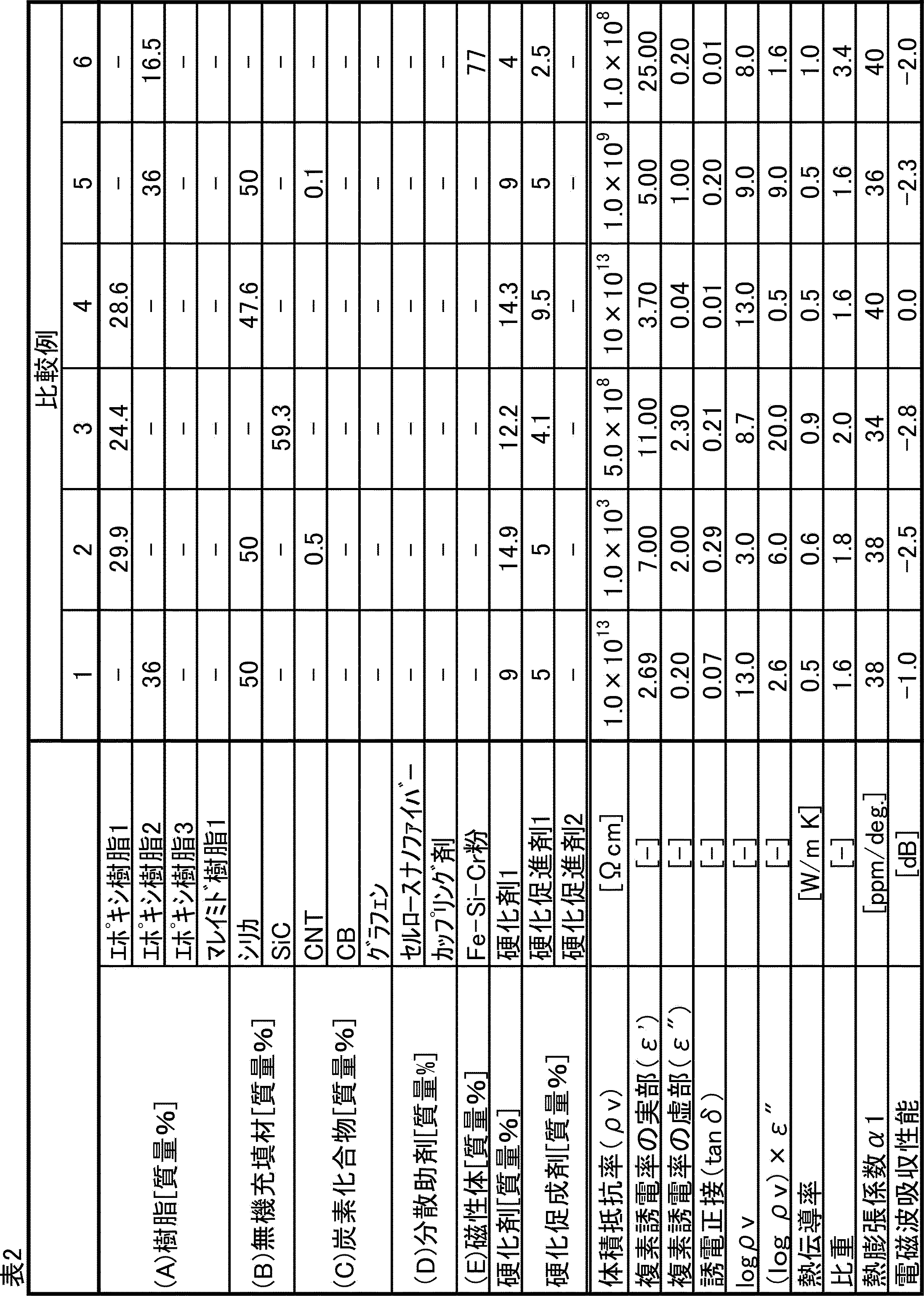
- Examples 1 to 22 and Comparative Examples 1 to 6) Each component of the type and blending amount shown in Table 1-1, Table 1-2 and Table 2 is charged into a Henschel mixer, mixed, and then charged into a twin-screw roll kneader heated to 110 ° C. to be uniformly. The heating and kneading work was carried out until it became. Next, the obtained heat-kneaded product was put into a cold roll, stretched into a sheet, and then pulverized to obtain a resin composition which is a molding material for an electromagnetic wave absorber.
- Epoxy resin 3 Epolite 400E; polyethylene glycol diglycidyl ether (mainly composed of the compound represented by the general formula (2)); manufactured by Kyoeisha Chemical Co., Ltd., epoxy equivalent: 277,
- the (A) resin ⁇ ′′ and ⁇ ′ and (B) the inorganic filler ⁇ ′′ were measured by the following methods.
- the resin (A) was added so that the amount of the curing agent 1 was equivalent to each resin, placed in a mold, and compression-molded (temperature; 175 ° C., pressure; 10 MPa) into a plate having a thickness of 1.0 mm.
- the inorganic filler (B) was placed in a mold and fired (temperature; 1500 ° C., 10 hours) so as to form a plate having a thickness of 1.0 mm after sintering.
- the obtained plate was measured by a network analyzer (Agilent PNA E8333B) and a rectangular waveguide (WRJ-10) at a temperature of 25 ° C. and a frequency in the range of 8.20 GHz or more and 12.40 GHz or less, respectively, at 10 GHz. The value of was calculated.
- a network analyzer Alignment PNA E8333B
- WRJ-10 rectangular waveguide
- CNT Carbon material
- CNT Carbon nanotube
- LUCAN LUCAN
- LG average fiber length: 30 ⁇ m
- aspect ratio 1500
- CB Carbon black
- CB30 CB30
- average particle size 50 nm
- Graphene Graphene nanoplatelet H: Made by XG-Science, Specific surface area (BET method): 30 m 2 / g
- [(D) Dispersion aid] -Cellulose nanofibers ELLEX-S; manufactured by Daio Paper Corporation, average fiber diameter: 20 to 200 nm -Coupling agent: SUMILINK (registered trademark) 100; thiosulfate S- (3-aminopropyl); manufactured by Sumitomo Chemical Co., Ltd.
- [Curing agent] -Curing agent 1 MEH7500; Triphenylmethane type phenol resin; manufactured by Meiwa Kasei Co., Ltd.
- volume resistivity ( ⁇ v) The volume resistivity at 150 ° C. was measured according to JIS K-6911: 2006 using a molded product having a thickness of 1.0 mm.
- a disk-shaped molded product having a specific gravity thickness of 2.0 mm and a diameter of 5 mm was obtained by compression molding (temperature; 180 ° C., pressure; 5 MPa).
- the specific gravity of the molded body is measured by measuring the mass and buoyancy in air and water using a balance. Asked.
- Electromagnetic wave absorption performance When a molded body with a thickness of 0.5 mm is installed between the high-frequency oscillating device and the receiving antenna, and the electromagnetic wave intensity when an electromagnetic wave with a frequency of 10 GHz is generated is with or without the molded body.
- the ratio (electromagnetic wave intensity when electromagnetic waves were absorbed by the molded body / electromagnetic wave intensity when there was no molded body) was taken as the electromagnetic wave absorbing capacity in dB.
- the electromagnetic wave intensity was measured according to "Journal of the Institute of Electronics, Information and Communication Engineers B Vol.J97-B No.3 pp.279-285".
- the molded product of the resin composition satisfying the above formula (1) and having the imaginary portion ( ⁇ ′′) larger than 1.25 is excellent in electromagnetic wave absorption performance in the high frequency band.
Landscapes
- Chemical & Material Sciences (AREA)
- Health & Medical Sciences (AREA)
- Chemical Kinetics & Catalysis (AREA)
- Medicinal Chemistry (AREA)
- Polymers & Plastics (AREA)
- Organic Chemistry (AREA)
- Engineering & Computer Science (AREA)
- Materials Engineering (AREA)
- Nanotechnology (AREA)
- Microelectronics & Electronic Packaging (AREA)
- Compositions Of Macromolecular Compounds (AREA)
- Shielding Devices Or Components To Electric Or Magnetic Fields (AREA)
- Non-Metallic Protective Coatings For Printed Circuits (AREA)
- Structures Or Materials For Encapsulating Or Coating Semiconductor Devices Or Solid State Devices (AREA)
Abstract
Description
[1]本開示の樹脂組成物は、該樹脂組成物の成形体が電磁波吸収体であり、前記成形体の25℃、10GHzにおける複素誘電率の虚部(ε′′)及び25℃における体積抵抗率(ρv)が、下記式(1)を満たし、前記虚部(ε′′)が1.25より大きい樹脂組成物である。
20<(log ρv)×ε′′<600 (1)
[2]本開示の電子部品は、上記[1]に記載の樹脂組成物の成形体を備える。
本開示の樹脂組成物は、高周波帯域での電磁波吸収性能に優れた成形体を得ることができる。
本開示の樹脂組成物は、該樹脂組成物の成形体が電磁波吸収体あり、前記成形体の25℃、10GHzにおける複素誘電率の虚部(ε′′)及び25℃における体積抵抗率(ρv)が、下記式(1)を満たす。また、前記虚部(ε′′)は1.25より大きい。
20<(log ρv)×ε′′<600 (1)
なお、前記ε′及びε′′は、導波管法により測定することができ、具体的には実施例に記載の方法により測定することができる。
なお、前記ρvはJIS K-6911:2006に準じて測定することができ、具体的には実施例に記載の方法により測定することができる。
なお、前記成形体の比重は、硬化した材料を空気中及び水中の質量および浮力を、天秤を用いて測定することで求めることができる。具体的には実施例に記載の方法により測定することができる。
なお、前記成形体の熱伝導率は、熱流エネルギーを熱線で与えた時の温度勾配を熱伝導率が既知の試料と比較して求める熱線法、均質な物質にレーザー等で瞬間的に高エネルギーを与え、その際測定される熱拡散率及び比熱をもとに熱伝導率を算出するレーザーフラッシュ法等により求めることができる。具体的には実施例に記載の方法により測定することができる。
熱膨張係数の低いインサートに成形体の熱膨張をできるだけ近づける、すなわち成形体の低熱膨張化が有用である。このような観点から、前記成形体の熱膨張率(α1:常温(25℃)からガラス転移温度までの間の熱膨張係数)は、1ppm/deg.以上であってもよく、3ppm/deg.以上であってもよい。また、前記成形体の熱膨張率は、40ppm/deg.以下であってもよく、35ppm/deg.以下であってもよい。前記成形体を封止材として用いる場合、前記成形体の熱膨張率は、18ppm/deg.以下であってもよく、15ppm/deg.以下であってもよい。
なお、前記成形体の熱膨張係数は、熱機械分析(Thermal Mechanical Analysis:TMA)による測定で得られるTMAチャートにおいて、25~60℃の接線の傾きから求めることができ、具体的には実施例に記載の方法により測定することができる。
前記(A)成分の樹脂は、熱硬化性樹脂および熱可塑性樹脂から選ばれる少なくとも1種である。熱硬化性樹脂としては、例えば、エポキシ樹脂、フェノール樹脂、イミド樹脂等が挙げられる。熱可塑性樹脂としては、例えば、ポリアミド、ポリカーボネート等が挙げられる。前記(A)成分の樹脂は、精密部品成形における粘度の観点から、熱硬化性樹脂であってもよく、電気絶縁性、耐熱性の観点から、エポキシ樹脂であってもよく、イミド樹脂であってもよい。
前記(A)成分の樹脂は、1種を用いてもよく、2種以上を組み合わせて使用してもよい。
なお、前記(A)成分の樹脂のε′及びε′′は、硬化剤とともに試験片板の成形後、導波管法により測定した値であり、具体的には実施例に記載された方法により測定された値である。
前記エポキシ樹脂は、例えばフェノールノボラック型エポキシ樹脂、クレゾールノボラック型エポキシ樹脂、ジシクロペンタジエン誘導体等の脂肪族系エポキシ樹脂、ビフェニル型、ビフェニルアラルキル型、ナフチル型およびビスフェノール型等の芳香族系エポキシ樹脂等が挙げられる。これらのエポキシ樹脂は1種のみで用いてもよいし、2種以上混合して用いてもよい。性状も特に制限はなく常温(25℃)で液状、固形いずれであっても構わない。例えば前記エポキシ樹脂は、液状ビスフェノール型エポキシ樹脂であってもよく、具体的には、ビスフェノールA型及びビスフェノールF型が挙げられる。液状ビスフェノール型エポキシ樹脂は、液状ビスフェノールA型エポキシ樹脂であってもよい。液状ビスフェノールA型エポキシ樹脂は、市販品として入手することができ、例えば、エポミック(登録商標)R140(三井化学(株)製)等が挙げられる。
なお、本開示において、液状ビスフェノール型エポキシ樹脂とは、25℃において液状を呈するビスフェノール型エポキシ樹脂を指す。
ここで、R1及びR2はそれぞれ独立に、炭素数1以上のアルキレン基を示す。m+nは、1以上50以下であってもよく、1以上20以下であってもよい。また、mは0以上49以下であってもよく、0以上19以下であってもよい。nは1以上50以下であってもよく、1以上20以下であってもよい。
m個のR1O基において、複数のR1は互いに同一のアルキレン基でもよく、炭素数の異なるアルキレン基であってもよい。また、n個のR2O基において、複数のR2は互いに同一のアルキレン基でもよく、炭素数の異なるアルキレン基であってもよい。


前記硬化剤としては、例えば、脂肪族アミン、芳香族アミン、ジシアンジアミド、ジヒドラジド化合物、酸無水物、フェノール樹脂などが挙げられる。これらは1種を用いてもよく、2種以上を組み合わせて使用してもよい。
前記硬化促進剤としては、ジクミルパーオキサイド、ジブチルパーオキサイド等の有機過酸化物;2-メチルイミダゾール、2-エチルイミダゾール等のイミダゾール化合物などが挙げられる。これらは1種を用いてもよく、2種以上を組み合わせて使用してもよい。
本開示の樹脂組成物が硬化剤を含有する場合、その含有量は該樹脂組成物全量に対し、1.0質量%以上20.0質量%以下であってもよく、2.0質量%以上18.0質量%以下であってもよく、3.0質量%以上15.0質量%以下であってもよい。また、本開示の樹脂組成物が硬化促進剤を含有する場合、その含有量は該樹脂組成物全量に対し、0.1質量%以上10.0質量%以下であってもよく、0.2質量%以上8.0質量%以下であってもよく、0.5質量%以上6.0質量%以下であってもよい。
前記(B)成分の無機充填材(後述する(C)成分を除く)は、電子部品で使用されるものであれば特に制限されないが、誘電率が高く、誘電正接が高い無機充填材であってもよく、例えば、シリカ、アルミナ、酸化チタン、チタン酸バリウム、窒化珪素、窒化アルミニウム、炭化ケイ素等が挙げられる。これらは1種を用いてもよく、2種以上を組み合わせて使用してもよい。前記(B)成分は、得られる成形体の高周波帯域での電磁波吸収性能を向上させる観点から、シリカ、アルミナ及び炭化ケイ素から選ばれる少なくとも1種であってもよく、炭化ケイ素であってもよい。
なお、前記(B)成分の無機充填材のε′′は、試験片板の焼成後、導波管法により測定した値であり、具体的には実施例に記載された方法により測定された値である。
なお、本明細書において、平均粒径とは、体積平均粒子径のことであり、(B)成分の無機充填材の平均粒径は、レーザー回折式粒度分布測定装置を用いて測定した、粒子の長径の平均値として算出することができる。
前記(C)成分の炭素材料は、電子部品で使用されるものであれば特に制限されなく、得られる成形体の誘電率及び損失誘電率を高くすることができる炭素材料であればよい。これにより、得られる成形体の高周波帯域での電磁波吸収性能を優れたものとすることができる。また、前記成形体が前記式(1)を満たしやすくなる。前記(C)成分の炭素材料としては、例えば、カーボンブラック、カーボンナノチューブ、フラーレン、グラファイト、グラフェンおよびこれらの誘導体等が挙げられる。これらは1種を用いてもよく、2種以上を組み合わせて使用してもよい。前記(C)成分の炭素材料は、カーボンブラック、カーボンナノチューブ及びグラフェンから選ばれる少なくとも1種であってもよく、カーボンナノチューブ及びグラフェンから選ばれる少なくとも1種であってもよい。
前記カーボンナノチューブの平均繊維径は、絶縁性の観点から、1nm以上30nm以下であってもよく、5nm以上25nm以下であってもよい。
前記カーボンナノチューブは、電磁波吸収能の観点から、アスペクト比(繊維径に対する繊維長さの比)が500以上10000以下であってもよく、1000以上5000以下であってもよい。
なお、カーボンナノチューブの平均繊維長さ及び平均繊維径は、走査型電子顕微鏡(SEM)によりカーボンナノチューブのサンプルを無作為に100個選択し、各サンプルの繊維長さ及び繊維径を測定し、それぞれ数平均を算出することにより求めることができる。また、カーボンナノチューブのアスペクト比は、前記で算出した平均繊維長さ及び平均繊維径の値から計算により求めることができる。
前記カーボンナノチューブは、単層構造および多層構造のいずれでもよく、価格及び入手のし易さの観点から、多層構造であってもよい。
前記カーボンブラックの平均粒径は、特に制限されないが、1nm以上80nm以下であってもよく、5nm以上60nm以下であってもよい。
なお、カーボンブラックの平均粒径は、無作為に100個の粒子を選び出して、透過型電子顕微鏡(TEM)により粒子の直径を測定し、その平均値を算出することにより求めることができる。
前記グラフェンの比表面積は、10m2/g以上3000m2/g以下であってもよく、20m2/g以上1500m2/g以下であってもよく、20m2/g以上500m2/g以下であってもよい。
前記比表面積は、窒素吸着によるBET 1点法により測定した値である。
なお、本明細書において、「グラフェン」とは、「10層以下のsp2結合炭素原子のシート状物質」を意味する。
分散液中のグラフェンの濃度は特に限定されないが、0.01質量%以上10質量%以下であってもよく、0.1質量%以上5質量%以下であってもよい。
本開示の樹脂組成物は、さらに(D)分散助剤を含んでもよい。(D)成分の分散助剤は、マトリクス樹脂に微粒子を安定的に高分散させるための材料であればいかなるものであってもよく、一般には一分子中に異なる反応性の官能基を併せ持つ界面活性剤、及びカップリング剤が用いられる。前記(D)成分の分散助剤としては、カルボン酸塩などのアニオン系界面活性剤、4級アンモニウム塩などのカチオン系界面活性剤等の界面活性剤;アミン系官能基とスルフィド系官能基を持つカップリング剤、セルロースナノファイバー等が挙げられる。前記(D)成分の分散助剤は、アミン系官能基とスルフィド系官能基を持つカップリング剤であってもよく、セルロースナノファイバーであってもよい。
前記セルロースナノファイバーの平均繊維長さは、作業性及び流動性の観点から、1μm以上100μm以下であってもよく、5μm以上50μm以下であってもよい。
前記セルロースナノファイバーの平均繊維径は、凝集体も含め、1nm以上1000nm以下であってもよく、4nm以上500nm以下であってもよい。前記平均繊維径が上記範囲にあることで、前記(C)成分の分散性を上げ誘電率を低下させることができる。
なお、セルロースナノファイバーの平均繊維長さ及び平均繊維径は、走査型電子顕微鏡(SEM)を用いて、前述のカーボンナノチューブの平均繊維長さ及び平均繊維径と同様の操作により測定することができる。
本開示の樹脂組成物は、(E)磁性体を含んでもよいが、含まなくてもよい。
(E)成分の磁性体は、一般に電磁波低減用に用いられる磁性材料からなる磁性体であれば特に制限されない。磁性材料としては、アモルファス磁性金属合金類、Ni-Fe系合金類、純鉄、軟鋼、ケイ素鋼(Fe-Si合金類)、Fe-Al合金類、Fe-Si-Al合金類、Co-Fe系合金類、カーボニル鉄等の軟磁性材料及びフェライトが挙げられる。これらは1種を用いてもよく、2種以上を組み合わせて使用してもよい。
本開示の一実施形態として、電磁波吸収材を半導体封止材として用いることができる。例えば、基板上に固定された半導体素子を、本開示の樹脂組成物で封止することにより、樹脂封止型の電子部品を得ることができる。
なお、電子部品を得るには、公知の成形方法が特に限定されずに用いられる。最も一般的な成形方法としては低圧トランスファー成形があるが、射出成形、注型成形、圧縮成形などによる成形も可能である。
前記電磁波吸収性能は、圧縮成形された厚さ0.5mmの成形体を高周波発振デバイスと受信用アンテナとの間に設置し、測定周波数10GHzの電磁波を発生させたときの電磁波強度を成形体がある場合とない場合で測定し、その比(成形体で電磁波吸収した時の電磁波強度/成形体が無い時の電磁波強度)をdB単位で表した値である。
なお、電磁波強度は「電子情報通信学会論文誌 B Vol.J97-B No.3 pp.279-285」に準じて測定することができる。
表1-1、表1-2及び表2に記載の種類及び配合量の各成分をヘンシェルミキサーに投入し、混合した後、110℃に加熱された二軸ロール混練装置に投入し、均一になるまで加熱混練作業を行った。次に、得られた加熱混練物を冷間ロールに投入し、シート状に引き伸ばした後に粉砕して、電磁波吸収材用の成形材料である樹脂組成物を得た。
・エポキシ樹脂1:エポミック(登録商標)R140;液状ビスフェノールA型エポキシ樹脂;三井化学(株)製、エポキシ当量:189、ε′′(25℃、10GHz)=0.04、ε′(25℃、10GHz)=2.5
・エポキシ樹脂2:リカレジン BEO-60E;ビスフェノールA骨格を有する液状エポキシ樹脂(ビスフェノールAビス(トリエチレングリコールグリシジルエーテル)エーテルを主成分とする)(前記一般式(1)で表される化合物);新日本理化(株)製、エポキシ当量:365、ε′′(25℃、10GHz)=0.20、ε′(25℃、10GHz)=3.0
・エポキシ樹脂3:エポライト400E;ポリエチレングリコールジグリシジルエーテル(前記一般式(2)で表される化合物を主成分とする);共栄社化学(株)製、エポキシ当量:277、ε′′(25℃、10GHz)=0.20、ε′(25℃、10GHz)=3.0
・イミド樹脂1:BANI-M;ビスアリルナジイミド;丸善石油化学(株)製、ε′′(25℃、10GHz)=0.07、ε′(25℃、10GHz)=2.5
・シリカ:FB105FC;デンカ(株)製、平均粒径:20μm、最大粒径:50μm、ε′′(25℃、10GHz)=0.001
・炭化ケイ素(SiC):ダイヤシック;屋久島電工(株)製、平均粒径:5μm、最大粒径:10μm、ε′′(25℃、10GHz)=2.0
・アルミナ:DAW07;デンカ(株)製、平均粒径:8μm、最大粒径:50μm、ε′′(25℃、10GHz)=0.1
前記(A)樹脂は、各樹脂に対し硬化剤1が当量となるように加え、型に入れ、それぞれ厚さ1.0mmの板に圧縮成形(温度;175℃、圧力;10MPa)した。
前記(B)無機充填材は、それぞれ型に入れ、焼結後の厚さが1.0mmの板になるよう焼成(温度;1500℃、10時間)した。
得られた板を用いて、ネットワークアナライザ(Agilent PNA E8363B)と方形導波管(WRJ-10)により、温度25℃で、周波数8.20GHz以上12.40GHz以下の範囲で測定し、10GHzにおけるそれぞれの値を求めた。
・カーボンナノチューブ(CNT):LUCAN;LG製、平均繊維長さ:30μm、平均繊維径:0.02μm、アスペクト比:1500
・カーボンブラック(CB):CB30;三菱化学(株)製、平均粒径:50nm
・グラフェン:グラフェン・ナノプレートレットH:XG-Science製、比表面積(BET法):30m2/g
・セルロースナノファイバー:ELLEX-S;大王製紙(株)製、平均繊維径:20~200nm
・カップリング剤:SUMILINK(登録商標)100;チオ硫酸S-(3-アミノプロピル);住友化学(株)製
・Fe-Si-Cr粉:日本アトマイズ加工(株)製、比重:7.6、平均粒径:11μm
・硬化剤1:MEH7500;トリフェニルメタン型フェノール樹脂;明和化成(株)製
・硬化促進剤1:キュアゾールC11Z;イミダゾール化合物;四国化成(株)製
・硬化促進剤2:パークミルD;有機過酸化物;日油(株)製
実施例1~22、及び比較例1~6で得られた樹脂組成物のそれぞれについて、厚さ0.5mm又は1.0mmの成形体を圧縮成形(温度;175℃、圧力;10MPa)した。以下の方法により、複素誘電率、体積抵抗率、熱伝導率及び電磁波吸収性能を測定した。評価結果を表1-1、表1-2及び表2に示す。
誘電特性は、厚さ1.0mmの成形体を用いて、ネットワークアナライザ(Agilent PNA E8363B)と方形導波管(WRJ-10)により、温度25℃で、周波数8.20GHz以上12.40GHz以下の範囲で測定を行い、10GHzにおけるそれぞれの値を求めた。
厚さ1.0mmの成形体を用いて、JIS K-6911:2006に準じて、150℃における体積抵抗率を測定した。
前記(1)で測定したε′′、及び前記(2)で測定したρvから、ε′′とρvの対数との積を算出した。
厚さ1.0mmの成形体の一方の面に、レーザー光を照射し、強度を周期的に変調させた熱流エネルギーを与え、温度センサを用いて、前記成形体の他方の面における温度応答の位相差を検出し、熱拡散率及び比熱を求め、熱伝導率を算出した。
厚さ2.0mm、直径5mmの円盤状の成形体を圧縮成形(温度;180℃、圧力;5MPa)により得た。前記成形体を用い、JIS Z 8807:2012 固体の密度及び比重の測定方法の液中ひょう量法に基づき、成形体を空気中及び水中の質量および浮力を、天秤を用いて測定することで比重を求めた。
TMA法により、熱分析装置(セイコーインスツル(株)製、商品名:SSC/5200)を用いて、昇温速度5℃/分として室温(25℃)から300℃まで昇温させ、得られたTMAチャートから、25~60℃の最も直線に近い部分の傾きを線膨張係数α1とした。
厚さ0.5mmの成形体を高周波発振デバイスと受信用アンテナの間に設置し、周波数10GHzの電磁波を発生させたときの電磁波強度を前記成形体がある場合とない場合とで測定し、その比(成形体で電磁波吸収した時の電磁波強度/成形体が無い時の電磁波強度)をdB単位で電磁波吸収能とした。
なお、電磁波強度は「電子情報通信学会論文誌 B Vol.J97-B No.3 pp.279-285」に準じて測定した。


1 リードフレーム
2 半導体素子
3 接着剤層
4 電極
5 リード部
6 ボンディングワイヤ
7 樹脂組成物の成形体(封止材)
Claims (9)
- 樹脂組成物の成形体が電磁波吸収体あり、
前記成形体の25℃、10GHzにおける複素誘電率の虚部(ε′′)及び25℃における体積抵抗率(ρv)が、下記式(1)を満たし、前記虚部(ε′′)が1.25より大きい樹脂組成物。
20<(log ρv)×ε′′<600 (1) - 前記成形体は、25℃、10GHzにおける複素誘電率の実部(ε′)が40未満である請求項1に記載の樹脂組成物。
- 前記成形体の熱膨張係数が1~40ppm/deg.である請求項1又は2記載の樹脂組成物。
- (A)熱硬化性樹脂および熱可塑性樹脂から選ばれる少なくとも1種である樹脂と、(B)無機充填材((C)成分を除く)と、(C)炭素材料とを含む請求項1~3のいずれか1項に記載の樹脂組成物。
- 前記(A)成分が、エポキシ樹脂である請求項4に記載の樹脂組成物。
- 前記エポキシ樹脂が、ポリオキシアルキレン構造を有する請求項5に記載の樹脂組成物。
- 前記(B)成分が、炭化ケイ素である請求項4~6のいずれか1項に記載の樹脂組成物。
- 前記(C)成分が、カーボンナノチューブ及びグラフェンから選ばれる少なくとも1種である請求項4~7のいずれか1項に記載の樹脂組成物。
- 請求項1~8のいずれか1項に記載の樹脂組成物の成形体を備える電子部品。
Priority Applications (5)
| Application Number | Priority Date | Filing Date | Title |
|---|---|---|---|
| US17/927,686 US20230174774A1 (en) | 2020-05-29 | 2021-05-25 | Resin composition and electronic component |
| KR1020227039688A KR102936799B1 (ko) | 2020-05-29 | 2021-05-25 | 수지 조성물 및 전자 부품 |
| JP2022526559A JP7737984B2 (ja) | 2020-05-29 | 2021-05-25 | 樹脂組成物及び電子部品 |
| EP21812236.4A EP4159816A4 (en) | 2020-05-29 | 2021-05-25 | Resin composition and electronic component |
| CN202180035450.2A CN115605549B (zh) | 2020-05-29 | 2021-05-25 | 树脂组合物和电子部件 |
Applications Claiming Priority (2)
| Application Number | Priority Date | Filing Date | Title |
|---|---|---|---|
| JP2020-094922 | 2020-05-29 | ||
| JP2020094922 | 2020-05-29 |
Publications (1)
| Publication Number | Publication Date |
|---|---|
| WO2021241541A1 true WO2021241541A1 (ja) | 2021-12-02 |
Family
ID=78744427
Family Applications (1)
| Application Number | Title | Priority Date | Filing Date |
|---|---|---|---|
| PCT/JP2021/019714 Ceased WO2021241541A1 (ja) | 2020-05-29 | 2021-05-25 | 樹脂組成物及び電子部品 |
Country Status (7)
| Country | Link |
|---|---|
| US (1) | US20230174774A1 (ja) |
| EP (1) | EP4159816A4 (ja) |
| JP (1) | JP7737984B2 (ja) |
| KR (1) | KR102936799B1 (ja) |
| CN (1) | CN115605549B (ja) |
| TW (2) | TWI862955B (ja) |
| WO (1) | WO2021241541A1 (ja) |
Cited By (1)
| Publication number | Priority date | Publication date | Assignee | Title |
|---|---|---|---|---|
| WO2025206306A1 (ja) * | 2024-03-29 | 2025-10-02 | 日本ゼオン株式会社 | 粉体、電磁波吸収体、及び溶融成形体の製造方法 |
Families Citing this family (2)
| Publication number | Priority date | Publication date | Assignee | Title |
|---|---|---|---|---|
| WO2022009555A1 (ja) * | 2020-07-07 | 2022-01-13 | 正毅 千葉 | 放熱材および電子デバイス |
| EP4421866A1 (en) * | 2023-02-24 | 2024-08-28 | Infineon Technologies AG | Radio frequency semiconductor device and method for fabricating a radio frequency semiconductor device |
Citations (8)
| Publication number | Priority date | Publication date | Assignee | Title |
|---|---|---|---|---|
| JP2001068889A (ja) | 1999-08-30 | 2001-03-16 | Daido Steel Co Ltd | 電磁波シールド材 |
| JP2005057093A (ja) | 2003-08-05 | 2005-03-03 | Kitagawa Ind Co Ltd | 電波吸収体、および電波吸収体の製造方法 |
| JP2008001757A (ja) * | 2006-06-20 | 2008-01-10 | Kyocera Chemical Corp | 半導体封止用樹脂組成物及び樹脂封止型半導体装置 |
| JP2011144235A (ja) * | 2010-01-13 | 2011-07-28 | Sumitomo Bakelite Co Ltd | 半導体封止用エポキシ樹脂組成物及び半導体装置 |
| JP2012209515A (ja) | 2011-03-30 | 2012-10-25 | Nitto Denko Corp | 電磁波吸収体及び電磁波吸収体の製造方法 |
| JP2019210447A (ja) * | 2018-06-04 | 2019-12-12 | 住友ベークライト株式会社 | 封止用樹脂組成物、これを用いる電子装置及び封止用樹脂組成物の製造方法 |
| JP2020111748A (ja) * | 2019-01-15 | 2020-07-27 | 京セラ株式会社 | 半導体封止用樹脂組成物およびそれを用いた半導体装置 |
| JP2020145270A (ja) * | 2019-03-05 | 2020-09-10 | 住友ベークライト株式会社 | 電子装置 |
Family Cites Families (11)
| Publication number | Priority date | Publication date | Assignee | Title |
|---|---|---|---|---|
| JP3916889B2 (ja) * | 2001-06-08 | 2007-05-23 | ソニー株式会社 | 半導体封止用樹脂組成物およびそれを用いた半導体装置 |
| JP2007036154A (ja) * | 2005-07-29 | 2007-02-08 | Bussan Nanotech Research Institute Inc | 電磁波吸収体 |
| KR101344644B1 (ko) * | 2006-06-06 | 2013-12-26 | 도다 고교 가부시끼가이샤 | 구상 소결 페라이트 입자 및 그것을 사용한 반도체 밀봉용 수지 조성물 및 그것을 사용하여 얻어지는 반도체 장치 |
| JP4798048B2 (ja) * | 2007-04-02 | 2011-10-19 | スターライト工業株式会社 | 電磁波遮蔽性と放熱性に優れた材料および成型品 |
| JP2011249614A (ja) * | 2010-05-27 | 2011-12-08 | Nitto Denko Corp | 誘電体シート及びその製造方法、並びに、電磁波吸収体 |
| CN105009225B (zh) * | 2013-02-21 | 2019-08-16 | 3M创新有限公司 | 具有电磁干扰减轻特性的聚合物复合物 |
| KR20180083866A (ko) * | 2015-11-18 | 2018-07-23 | 스미토모 세이카 가부시키가이샤 | 에폭시 수지 조성물, 그 제조 방법 및 해당 조성물의 용도 |
| JP6414258B2 (ja) * | 2016-04-01 | 2018-10-31 | 三菱ケミカル株式会社 | 樹脂組成物 |
| KR102561855B1 (ko) | 2017-03-30 | 2023-08-02 | 아지노모토 가부시키가이샤 | 페이스트상 수지 조성물 |
| JP7213621B2 (ja) * | 2018-04-04 | 2023-01-27 | デクセリアルズ株式会社 | 半導体装置 |
| JP2020072196A (ja) * | 2018-10-31 | 2020-05-07 | 北川工業株式会社 | 熱伝導シート |
-
2021
- 2021-05-25 JP JP2022526559A patent/JP7737984B2/ja active Active
- 2021-05-25 EP EP21812236.4A patent/EP4159816A4/en active Pending
- 2021-05-25 WO PCT/JP2021/019714 patent/WO2021241541A1/ja not_active Ceased
- 2021-05-25 CN CN202180035450.2A patent/CN115605549B/zh active Active
- 2021-05-25 KR KR1020227039688A patent/KR102936799B1/ko active Active
- 2021-05-25 US US17/927,686 patent/US20230174774A1/en active Pending
- 2021-05-26 TW TW111127067A patent/TWI862955B/zh active
- 2021-05-26 TW TW110119033A patent/TWI774393B/zh active
Patent Citations (8)
| Publication number | Priority date | Publication date | Assignee | Title |
|---|---|---|---|---|
| JP2001068889A (ja) | 1999-08-30 | 2001-03-16 | Daido Steel Co Ltd | 電磁波シールド材 |
| JP2005057093A (ja) | 2003-08-05 | 2005-03-03 | Kitagawa Ind Co Ltd | 電波吸収体、および電波吸収体の製造方法 |
| JP2008001757A (ja) * | 2006-06-20 | 2008-01-10 | Kyocera Chemical Corp | 半導体封止用樹脂組成物及び樹脂封止型半導体装置 |
| JP2011144235A (ja) * | 2010-01-13 | 2011-07-28 | Sumitomo Bakelite Co Ltd | 半導体封止用エポキシ樹脂組成物及び半導体装置 |
| JP2012209515A (ja) | 2011-03-30 | 2012-10-25 | Nitto Denko Corp | 電磁波吸収体及び電磁波吸収体の製造方法 |
| JP2019210447A (ja) * | 2018-06-04 | 2019-12-12 | 住友ベークライト株式会社 | 封止用樹脂組成物、これを用いる電子装置及び封止用樹脂組成物の製造方法 |
| JP2020111748A (ja) * | 2019-01-15 | 2020-07-27 | 京セラ株式会社 | 半導体封止用樹脂組成物およびそれを用いた半導体装置 |
| JP2020145270A (ja) * | 2019-03-05 | 2020-09-10 | 住友ベークライト株式会社 | 電子装置 |
Non-Patent Citations (2)
| Title |
|---|
| IEICE TRANSACTIONS ON FUNDAMENTALS OF ELECTRONICS, COMMUNICATIONS, AND COMPUTER SCIENCES B, vol. J97-B, no. 3, pages 279 - 285 |
| See also references of EP4159816A4 |
Cited By (1)
| Publication number | Priority date | Publication date | Assignee | Title |
|---|---|---|---|---|
| WO2025206306A1 (ja) * | 2024-03-29 | 2025-10-02 | 日本ゼオン株式会社 | 粉体、電磁波吸収体、及び溶融成形体の製造方法 |
Also Published As
| Publication number | Publication date |
|---|---|
| JPWO2021241541A1 (ja) | 2021-12-02 |
| EP4159816A4 (en) | 2024-11-06 |
| TW202205561A (zh) | 2022-02-01 |
| TW202243147A (zh) | 2022-11-01 |
| JP7737984B2 (ja) | 2025-09-11 |
| CN115605549A (zh) | 2023-01-13 |
| KR102936799B1 (ko) | 2026-03-09 |
| KR20230008096A (ko) | 2023-01-13 |
| CN115605549B (zh) | 2025-03-21 |
| TWI774393B (zh) | 2022-08-11 |
| EP4159816A1 (en) | 2023-04-05 |
| TWI862955B (zh) | 2024-11-21 |
| US20230174774A1 (en) | 2023-06-08 |
Similar Documents
| Publication | Publication Date | Title |
|---|---|---|
| TWI700243B (zh) | 六方晶氮化硼粉末及其製造方法以及使用其之組成物及散熱材 | |
| Huang et al. | A novel h-BN–RGO hybrids for epoxy resin composites achieving enhanced high thermal conductivity and energy density | |
| JP7737984B2 (ja) | 樹脂組成物及び電子部品 | |
| US20220169832A1 (en) | Spherical silica powder | |
| JP5707052B2 (ja) | 樹脂複合組成物及びその用途 | |
| KR101612596B1 (ko) | 적층체 및 파워 반도체 모듈용 부품의 제조 방법 | |
| JP2011208007A (ja) | 樹脂複合組成物及びその用途 | |
| JP7598197B2 (ja) | 5g通信用アンテナアレイ、アンテナ構造、ノイズ抑制熱伝導シート及び熱伝導シート | |
| US10696840B2 (en) | Resin composition for semiconductor encapsulation and semiconductor device | |
| TWI869662B (zh) | 氮化硼粉末及樹脂組成物 | |
| Li et al. | High-performance epoxy resin/silica coated flake graphite composites for thermal conductivity and electrical insulation | |
| JP5803348B2 (ja) | ポリマーナノコンポジット樹脂組成物 | |
| KR101683633B1 (ko) | 분산안정성과 방열특성이 우수한 그라펜 첨가 액정 에폭시계 접착제의 사용방법 | |
| JP7348847B2 (ja) | 半導体封止用樹脂組成物およびそれを用いた半導体装置 | |
| KR20230156793A (ko) | 질화붕소 입자, 그 제조 방법, 및 수지 조성물 | |
| Ni et al. | Coordinating of thermal and dielectric properties for cyanate ester composites filled with silica‐coated sulfonated graphene oxide hybrids | |
| KR102935933B1 (ko) | 질화붕소 분말 및 수지 조성물 | |
| JP5095136B2 (ja) | 半導体封止用樹脂組成物の製造方法 | |
| Takahashi et al. | Heat-resistant epoxy-silicon hybrid materials for printed wiring boards | |
| JP7850402B2 (ja) | 電磁干渉抑制材料 | |
| KR20220129549A (ko) | 열전도성 시트, 적층체, 및 반도체 장치 | |
| JP2025117061A (ja) | 電磁波抑制樹脂組成物及びその硬化物 |
Legal Events
| Date | Code | Title | Description |
|---|---|---|---|
| 121 | Ep: the epo has been informed by wipo that ep was designated in this application |
Ref document number: 21812236 Country of ref document: EP Kind code of ref document: A1 |
|
| ENP | Entry into the national phase |
Ref document number: 20227039688 Country of ref document: KR Kind code of ref document: A |
|
| ENP | Entry into the national phase |
Ref document number: 2022526559 Country of ref document: JP Kind code of ref document: A |
|
| NENP | Non-entry into the national phase |
Ref country code: DE |
|
| ENP | Entry into the national phase |
Ref document number: 2021812236 Country of ref document: EP Effective date: 20230102 |
|
| WWG | Wipo information: grant in national office |
Ref document number: 202180035450.2 Country of ref document: CN |
|
| WWR | Wipo information: refused in national office |
Ref document number: 1020227039688 Country of ref document: KR |