WO2021245921A1 - 光受信器、及び光受信方法 - Google Patents
光受信器、及び光受信方法 Download PDFInfo
- Publication number
- WO2021245921A1 WO2021245921A1 PCT/JP2020/022360 JP2020022360W WO2021245921A1 WO 2021245921 A1 WO2021245921 A1 WO 2021245921A1 JP 2020022360 W JP2020022360 W JP 2020022360W WO 2021245921 A1 WO2021245921 A1 WO 2021245921A1
- Authority
- WO
- WIPO (PCT)
- Prior art keywords
- optical
- signal
- component
- subcarrier
- electric signal
- Prior art date
- Legal status (The legal status is an assumption and is not a legal conclusion. Google has not performed a legal analysis and makes no representation as to the accuracy of the status listed.)
- Ceased
Links
Images







Classifications
-
- H—ELECTRICITY
- H04—ELECTRIC COMMUNICATION TECHNIQUE
- H04B—TRANSMISSION
- H04B10/00—Transmission systems employing electromagnetic waves other than radio-waves, e.g. infrared, visible or ultraviolet light, or employing corpuscular radiation, e.g. quantum communication
- H04B10/60—Receivers
- H04B10/61—Coherent receivers
- H04B10/64—Heterodyne, i.e. coherent receivers where, after the opto-electronic conversion, an electrical signal at an intermediate frequency [IF] is obtained
-
- H—ELECTRICITY
- H04—ELECTRIC COMMUNICATION TECHNIQUE
- H04B—TRANSMISSION
- H04B10/00—Transmission systems employing electromagnetic waves other than radio-waves, e.g. infrared, visible or ultraviolet light, or employing corpuscular radiation, e.g. quantum communication
- H04B10/27—Arrangements for networking
- H04B10/272—Star-type networks or tree-type networks
Definitions
- the present invention relates to an optical receiver and an optical receiving method.
- a carrier-wave suppression type optical subcarrier multiplexed signal using an optical IQ modulator as an optical transmitter is used.
- the optical receiver demodulates the optical subcarrier multiplex signal by using optical intradyne detection. This reduces the influence of signal performance deterioration due to interference noise during optical intradyne detection.
- FIG. 16 is a block diagram showing a functional configuration of the conventional optical transmitter 100.
- the optical transmitter 100 is a transmitter for generating a carrier wave suppression type optical subcarrier multiplex signal.
- the optical transmitter 100 includes a serial parallel converter 101, symbol mappers 102-1 to 102-n (n is an integer of 2 or more), frequency shift units 103-1 to 103-n, an adder 104, and a D / A (Digital).
- -to-Analog) A converter 105-1 to 105-2, a laser 106, and an optical IQ modulator 107 are provided.
- the serial-parallel conversion unit 101 parallelizes the data signal input from the outside into 2N columns.
- the serial-parallel conversion unit 101 parallelizes the data signals by the number of symbol mappers 102-1 to 102-n.
- N is an integer of 1 or more.
- the symbol mappers 102-1 to 102-n map the parallelized data signals according to the modulation method.
- the mapped data signal is input to the frequency shift units 103-1 to 103-n.
- the frequency shift units 103-1 to 103-n move the input data signals so as not to overlap on the frequency axis.
- the adder 104 generates a frequency-multiplexed signal by adding data signals output from each of the frequency shift units 103-1 to 103-n.
- the D / A converters 105-1 to 105-2 convert the frequency-multiplexed signal into digital-to-analog.
- the D / A converter 105-1 converts the real part (I component) of the frequency-multiplexed signal into digital-to-analog.
- the D / A converter 105-2 converts the imaginary part (Q component) of the frequency-multiplexed signal into digital-to-analog.
- the laser 106 outputs an optical signal having a frequency of f 0 to the optical IQ modulator 107.
- the optical IQ modulator 107 generates a modulated signal by photomodulating the output light of the laser 106 with a subcarrier multiplexed signal divided into an I component and a Q component.
- the optical IQ modulator 107 transmits the generated modulated signal to the optical receiver via an optical fiber.
- the parallel data of the 2N column is at the frequency position numbered by # 1, ..., # N-1, #N, # N + 1, # N + 2, ..., # 2N. It is superimposed on a certain optical subcarrier.
- the optical transmitter 100 does not utilize all optical subcarriers as shown in FIG. 16 (A). Serial-parallel conversion is performed according to the optical subcarrier used.
- FIG. 16B shows an example in which only the optical subcarrier of # N-1 is used.
- FIG. 17 is a block diagram showing the functional configuration of the conventional optical receiver 200.
- the optical receiver 200 includes a configuration of a digital coherent receiver by general optical intradyne detection.
- the optical receiver 200 includes a PBS (Polarization Beam Splitter) 201, a local oscillation light source 202, a PBS 203, an optical 90-degree hybrid detector 204-1 to 204-2, and an A / D (Analog-to-Digital) converter 205-1. It is provided with ⁇ 205-2, A / D converters 206-1 to 206-2, and a digital signal processing unit 207.
- PBS Polarization Beam Splitter
- PBS201 is a polarization splitter.
- the PBS 201 inputs the modulated signal transmitted from the optical transmitter 100.
- PBS201 separates the input modulation signal into a horizontally polarized optical signal and a vertically polarized optical signal.
- the PBS 201 outputs a horizontally polarized optical signal to the optical 90-degree hybrid detector 204-1 and outputs a vertically polarized optical signal to the optical 90-degree hybrid detector 204-2.
- the local oscillation light source 202 outputs local light emission.
- PBS203 is a polarization splitter.
- the PBS 203 inputs the local emission output from the local oscillation light source 202.
- the PBS 203 separates the input local emission into a horizontally polarized light signal and a vertically polarized light signal.
- the PBS 203 outputs a horizontally polarized optical signal to the optical 90-degree hybrid detector 204-1 and outputs a vertically polarized optical signal to the optical 90-degree hybrid detector 204-2.
- the optical 90 degree hybrid detector 204-1 inputs and processes an optical signal of horizontally polarized waves.
- the optical 90 degree hybrid detector 204-1 includes splitters 208-1 to 208-2, ⁇ / 2 delayers 209, couplers 210-1 to 210-2, and balanced receivers 211-1 to 211-2.
- Splitter 208-1 inputs a horizontally polarized optical signal output from PBS201.
- the splitter 208-1 branches the input horizontally polarized optical signal and outputs it to the couplers 210-1 and 210-2.
- the splitter 208-2 inputs a horizontally polarized optical signal output from the PBS 203.
- the splitter 208-2 branches the input horizontally polarized optical signal and outputs it to the coupler 210-1 and the ⁇ / 2 delay device 209.
- the ⁇ / 2 delay device 209 delays the horizontally polarized optical signal output by the splitter 208-2 by ⁇ / 2 and outputs it to the coupler 210-2.
- the coupler 210-1 generates interference light by merging and interfering with the horizontally polarized light signal output by the splitter 208-1 and the horizontally polarized light signal output by the splitter 208-2.
- the coupler 210-1 branches the generated interference light into two interference lights and outputs the generated interference light to the balanced receiver 211-1.
- the coupler 210-2 causes the horizontally polarized optical signal output by the splitter 208-1 to interfere with the horizontally polarized optical signal output by the ⁇ / 2 delayer 209 and delayed by ⁇ / 2 minutes. This produces interference light.
- the coupler 210-2 branches the generated interference light into two interference lights and outputs the generated interference light to the balanced receiver 211-2.
- the balanced receiver 211-1 converts the two interference lights output by the coupler 210-1 into an electric signal.
- the balanced receiver 211-1 detects the difference between the converted electric signals as an in-phase component, that is, an I component, and outputs the difference to the A / D converter 205-1.
- the balanced receiver 211-2 converts the two interference lights output by the coupler 210-2 into an electric signal.
- the balanced receiver 211-2 detects the difference between the converted electric signals as an orthogonal component, that is, a Q component, and outputs the difference to the A / D converter 205-2.
- the A / D converter 205-1 samples the analog electric signal of the I component and outputs it to the digital signal processing unit 207 as a digital sampling signal.
- the A / D converter 205-2 samples the analog electric signal of the Q component and outputs it to the digital signal processing unit 207 as a digital sampling signal.
- the optical 90 degree hybrid detector 204-2 inputs and processes a vertically polarized optical signal.
- the optical 90 degree hybrid detector 204-2 includes splitters 212-1 to 212-2, ⁇ / 2 delayers 213, couplers 214-1 to 214-2, and balanced receivers 215-1 to 215-2.
- Splitter 212-1 inputs a vertically polarized optical signal output from PBS201.
- the splitter 212-1 branches the input vertically polarized optical signal and outputs it to the couplers 214-1 and 214-2.
- the splitter 212-2 inputs a vertically polarized optical signal output from the PBS 203.
- the splitter 212-2 branches the input vertically polarized optical signal and outputs it to the coupler 214-1 and the ⁇ / 2 delayer 213.
- the ⁇ / 2 delay device 213 delays the vertically polarized optical signal output by the splitter 212-2 by ⁇ / 2 and outputs it to the coupler 214-2.
- the coupler 214-1 generates interference light by merging and interfering with the vertically polarized light signal output by the splitter 212-1 and the vertically polarized light signal output by the splitter 212-2.
- the coupler 214-1 branches the generated interference light into two interference lights and outputs the generated interference light to the balanced receiver 215-1.
- the coupler 214-2 causes the vertically polarized light signal output by the splitter 212-1 and the vertically polarized light signal output by the ⁇ / 2 delayer 213 to be delayed by ⁇ / 2 to interfere with each other. This produces interference light.
- the coupler 214-2 branches the generated interference light into two interference lights and outputs the generated interference light to the balanced receiver 215-2.
- the balanced receiver 215-1 converts the two interference lights output by the coupler 214-1 into an electric signal.
- the balanced receiver 215-1 detects the difference between the converted electric signals as an in-phase component, that is, an I component, and outputs the difference to the A / D converter 206-1.
- the balanced receiver 215-2 converts the two interference lights output by the coupler 214-2 into an electric signal.
- the balanced receiver 215-2 detects the difference between the converted electric signals as an orthogonal component, that is, a Q component, and outputs the difference to the A / D converter 206-2.
- the A / D converter 206-1 samples the analog electric signal of the I component and outputs it to the digital signal processing unit 207 as a digital sampling signal.
- the A / D converter 206-2 samples the analog electric signal of the Q component and outputs it to the digital signal processing unit 207 as a digital sampling signal.
- the digital signal processing unit 207 inputs digital sampling signals output from each of the A / D converters 205-1 to 205-4.
- the digital signal processing unit 207 demodulates the input sampling signal.
- the processing performed by the optical receiver 200 is the same as that of a general intradyne receiver used in digital coherent transmission.
- the carrier wave is suppressed as shown in FIG. 16 by performing optical subcarrier modulation using an optical IQ modulator, and interference during optical reception is performed.
- the influence of noise can be reduced (see Non-Patent Document 1).
- optical intradyne detector used in the conventional technology has a problem that the configuration is complicated and it is expensive to use in the access system.
- an object of the present invention is to provide a technique capable of deteriorating signal performance due to interference noise when optical reception is performed by coherent detection at low cost.
- One aspect of the present invention is a heterodyne detection unit that converts a subcarrier multiplexed signal in which a plurality of optical signals transmitted from a plurality of optical transmitters are multiplexed into an electric signal in the intermediate frequency band by heterodyne detection, and an intermediate frequency band.
- a filter unit that extracts a subcarrier component excluding a carrier component from the electric signal converted to the above, an analog digital conversion unit that converts the signal of the subcarrier component extracted by the filter unit into analog digital, and the analog digital.
- It is an optical receiver including a digital signal processing unit that performs digital signal processing for each subcarrier using a digital signal converted by the conversion unit.
- a subcarrier multiplexed signal in which a plurality of optical signals transmitted from a plurality of optical transmitters are multiplexed is converted into an electric signal in the intermediate frequency band by heterodyne detection, and converted into the intermediate frequency band.
- the subcarrier component excluding the carrier wave component is extracted from the electric signal, the extracted signal of the subcarrier component is analog-digitally converted, and the digital signal converted by the analog-digital conversion is used to digitalize each subcarrier.
- the carrier in the third embodiment shows an example of setting the f 0 frequencies below position.
- the carrier in the third embodiment shows an example of setting the f 0 frequencies above position. It is a block diagram which shows the functional structure of the optical receiver in 4th Embodiment.
- ONU subscriber line terminal devices
- OLT subscriber line end station device
- OLT optical receiver
- an optical intensity modulator is used as an optical transmitter
- a heterodyne detector is used as an optical receiver.
- Each of the ONUs transmits a modulated signal in which the subcarrier is modulated by the optical intensity modulator to the OLT.
- the modulated signals transmitted from each of the ONUs are multiplexed in the optical splitter and input to the OLT.
- the subcarrier multiplex signal is optical heterodyne detection.
- the optical receiver removes the carrier component converted into the intermediate frequency band by the bandpass filter in the electric stage. Then, the optical receiver extracts the subcarrier on which the transmission data is superimposed.
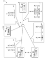
- FIG. 1 is a diagram showing a system configuration of the optical transmission system 1 according to the first embodiment.
- the optical transmission system 1 includes N ONU2-1 to 2-N and one OLT3. ONU2-1 to 2-N and OLT3 are connected by an optical fiber via an optical splitter 4.
- the optical splitter 4 multiplexes the optical signals output from each of ONU2-1 to 2-N and outputs them to the OLT3.
- the optical splitter 4 demultiplexes the optical signal output from the OLT 3 and outputs it to ONU2-1 to 2-N.
- the description will focus on the uplink signal transmission from ONU2-1 to 2-N to OLT3.
- ONU2-1 to 2-N are not particularly distinguished in the following description, they are described as ONU2.
- the ONU2 is installed, for example, in the home of a subscriber who receives a communication service.
- the ONU 2 includes an optical transmitter 10.
- the optical transmitter 10 transmits an optical signal.
- the OLT 3 is installed, for example, in a containment station.
- the OLT 3 includes an optical receiver 30.
- the optical receiver 30 receives the subcarrier multiplexed signal multiplexed by the optical splitter 4.
- the optical transmitters 10-1 to 2-N of each ONU2-1 to 2-N are modulated by optical modulation of the laser output of the same frequency (f 0 ) by the subcarrier of the electric stage on which the transmission data is superimposed. Generate a signal.
- the modulated signals generated by each ONU2 are merged by the optical splitter 4, optically subcarrier-multiplexed, and transmitted to the OLT3.
- FIG. 1 shows a case where ONU2-1 to 2-N generate optical subcarriers at positions of f 0 ⁇ ⁇ f, f 0 ⁇ 2 ⁇ f, ..., F 0 ⁇ N ⁇ f, respectively.
- ONU2-1 produces an optical subcarrier at f 0 ⁇ ⁇ f
- ONU2-2 produces an optical subcarrier at f 0 ⁇ 2 ⁇ f
- ONU2-N produces light at f 0 ⁇ N ⁇ f.
- Generate subcarriers that is, although the case where one ONU2 generates one optical subcarrier is shown, one ONU2 may generate a plurality of optical subcarriers.
- each of ONU2-1 to 2-N transmits the modulation signal of the optical subcarrier shown in FIG. 1, the carrier of the subcarrier multiplexed signal received by OLT 3 is superimposed on the same frequency (f 0).
- FIG. 2 is a block diagram showing a functional configuration of the optical transmitter 10 in the first embodiment.
- the optical transmitter 10 includes a symbol mapper 11, an oscillator 12, a modulation circuit 13, a laser 14, and an optical intensity modulator 15.
- FIG. 2 shows the configuration of an optical transmitter by an analog method.
- the symbol mapper 11 maps the data signal input from the outside according to the modulation method.
- the modulation circuit 13 modulates the subcarriers output from the oscillator 12 with the data mapped by the symbol mapper 11.
- the laser 14 outputs an optical signal having a frequency f 0 to the light intensity modulator 15.
- the light intensity modulator 15 photomodulates the output light of the laser 14 with a subcarrier modulated by the modulation circuit 13. Specifically, the light intensity modulator 15 generates a modulated signal by photomodulating the intensity of the output light of the laser 14 with a subcarrier modulated by the modulation circuit 13.
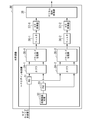
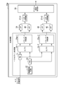
- FIG. 3 is a block diagram showing the functional configuration of the optical receiver 30 in the first embodiment.
- the optical receiver 30 is a digital coherent receiver that performs optical heterodyne detection.
- the optical receiver 30 includes a PBS 31, a local oscillation light source 32, a PBS 33, a coupler 34-1, 34-2, a balanced receiver 35-1, 35-2, a filter 36-1, 36-2, and an A / D converter. It includes 37-1, 37-2 and a digital signal processing unit 38.
- the PBS 31, the local oscillation light source 32, the PBS 33, the couplers 34-1, 34-2, and the balanced receivers 35-1, 35-2 are examples of the heterodyne detection unit.
- PBS31 is a polarization splitter.
- the PBS 31 inputs a subcarrier multiplexing signal multiplexed by the optical splitter 4.
- the PBS 31 separates the input subcarrier multiplex signal into a horizontally polarized subcarrier multiplex signal and a vertically polarized subcarrier multiplex signal.
- the PBS 31 outputs a horizontally polarized subcarrier multiplex signal to the coupler 34-1 and outputs a vertically polarized subcarrier multiplex signal to the coupler 34-2.
- the local oscillation light source 32 outputs local light emission used for optical heterodyne detection.
- the PBS 33 is a polarization splitter.
- the PBS 33 inputs the local emission output from the local oscillation light source 32.
- the PBS 33 separates the input local emission into a horizontally polarized light signal and a vertically polarized light signal.
- the PBS 33 outputs a horizontally polarized optical signal to the coupler 34-1 and outputs a vertically polarized optical signal to the coupler 34-2.
- the coupler 34-1 generates interference light by merging and interfering with the horizontally polarized subcarrier multiplex signal output by PBS 31 and the horizontally polarized optical signal output by PBS 33.
- the coupler 34-1 branches the generated interference light into two interference lights and outputs the generated interference light to the balanced receiver 35-1.
- the coupler 34-2 generates interference light by merging and interfering with the vertically polarized subcarrier multiplex signal output by PBS 31 and the vertically polarized optical signal output by PBS 33.
- the coupler 34-2 branches the generated interference light into two interference lights and outputs the generated interference light to the balanced receiver 35-2.
- the balanced receiver 35-1 converts the two interference lights output by the coupler 34-1 into an electric signal.
- the balanced receiver 35-1 outputs the difference between the converted electric signals to the filter 36-1.
- the balanced receiver 35-2 converts the two interference lights output by the coupler 34-2 into an electric signal.
- the balanced receiver 35-2 outputs the difference between the converted electric signals to the filter 36-2.
- the filter 36-1 filters an electric signal representing the difference between the two interference lights output from the balanced receiver 35-1.
- the filter 36-1 is an LPF (Low-Pass Filter) or an HPF (High-Pass Filter).
- the LPF and HPF may use an analog circuit as shown in the figure, but may be performed by dental signal processing.
- the filter 36-1 extracts only the upper wave band component (+) of the subcarrier multiplexing (SCM) signal by LPF or the lower wave band component (-) by HPF. It is more economical to extract the upper wave band component because it can be received by using a lower frequency A / D converter.
- SCM subcarrier multiplexing
- the filter 36-2 filters an electric signal representing the difference between the two interference lights output from the balanced receiver 35-2.
- the filter 36-2 is an LPF or an HPF.
- the A / D converter 37-1 analog-digitally converts the upper wave band component (+) or the lower wave band component ( ⁇ ) extracted by the filter 36-1 to generate a digital signal.
- the A / D converter 37-2 analog-digitally converts the upper wave band component (+) or the lower wave band component ( ⁇ ) extracted by the filter 36-2 to generate a digital signal.
- the digital signal processing unit 38 inputs the digital signals output from each of the A / D converters 37-1 to 37-2.
- the digital signal processing unit 38 demodulates the input digital signal by performing digital signal processing for each subcarrier.
- Modulated subcarrier signals generated by the optical transmitter 10 shown in FIG. 2, with respect to the carrier frequency f 0, is produced in a range of ⁇ B.
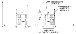
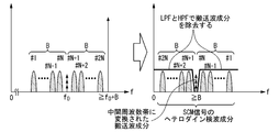
- FIG. 4 shows an example when the carrier wave is set at a frequency position of f 0 + B or higher
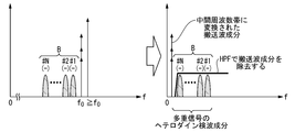
- FIG. 5 shows an example of a case where the carrier wave is set at a frequency position of f 0 ⁇ B or lower.
- the left figure is a diagram showing the frequency of the subcarrier multiplex signal received by the optical receiver 30, and the right figure is a diagram for explaining the specific processing of the optical receiver 30. Is.
- the right figure of FIG. 4 shows an example in which the lower wave band component (-) of the subcarrier multiplex signal converted into the signal of the intermediate frequency band by the optical heterodyne detection and the carrier wave component are removed by LPF.
- the right figure of FIG. 5 shows an example in which the upper wave band component (+) of the subcarrier multiplex signal converted into the signal of the intermediate frequency band by the optical heterodyne detection and the carrier wave component are removed by LPF.
- FIG. 6 is a sequence diagram showing a processing flow of the optical transmission system 1 according to the first embodiment.
- the optical transmission system 1 includes two optical transmitters 10 (optical transmitters 10-1 and 10-2) will be described as an example.
- the functional part of each optical transmitter 10 will be described with a branch number.
- the symbol mapper 11-1 of the optical transmitter 10-1 maps the data signal input from the outside according to the modulation method (step S101).
- the symbol mapper 11-1 outputs the mapped data to the modulation circuit 13-1.
- the modulation circuit 13-1 inputs the subcarrier of the frequency ⁇ f output from the oscillator 12-1 and the mapped data output from the symbol mapper 11-1.
- the modulation circuit 13-1 modulates the input subcarrier with the mapped data (step S102).
- the modulation circuit 13-1 outputs the modulated subcarrier to the light intensity modulator 15-1.
- the optical intensity modulator 15-1 inputs an optical signal having a frequency f 0 output from the laser 14-1 and a modulated subcarrier output from the modulation circuit 13-1.
- the light intensity modulator 15-1 photomodulates the intensity of the input output light of the laser 14-1 with the modulated subcarrier output from the modulation circuit 13-1. As a result, the light intensity modulator 15-1 generates a modulated signal (step S103).
- the symbol mapper 11-2 of the optical transmitter 10-2 maps the data signal input from the outside according to the modulation method (step S104).
- the symbol mapper 11-2 outputs the mapped data to the modulation circuit 13-2.
- the modulation circuit 13-2 inputs the subcarrier having a frequency of 2 ⁇ f output from the oscillator 12-2 and the mapped data output from the symbol mapper 11-2.
- the modulation circuit 13-2 modulates the input subcarrier with the mapped data (step S105).
- the modulation circuit 13-2 outputs the modulated subcarrier to the light intensity modulator 15-2.
- the optical intensity modulator 15-2 inputs an optical signal having a frequency f 0 output from the laser 14-2 and a modulated subcarrier output from the modulation circuit 13-2.
- the light intensity modulator 15-2 photomodulates the intensity of the input output light of the laser 14-2 with the modulated subcarrier output from the modulation circuit 13-2. As a result, the light intensity modulator 15-2 generates a modulated signal (step S106).
- the optical transmitter 10-1 transmits the modulated signal generated by the optical intensity modulator 15-1 (step S107).
- the optical transmitter 10-2 transmits the modulated signal generated by the optical intensity modulator 15-2 (step S108).
- the optical splitter 4 receives the modulated signals output from the optical transmitters 10-1 and 10-2, respectively.
- the optical splitter 4 multiplexes each received modulation signal to generate a subcarrier multiplexed signal (step S109).
- the optical splitter 4 transmits the generated subcarrier multiplex signal to the optical receiver 30 (step S110).
- the optical receiver 30 receives the subcarrier multiplex signal output from the optical splitter 4.
- the optical receiver 30 acquires a horizontally polarized electric signal and a vertically polarized electric signal by performing optical heterodyne detection of the received subcarrier multiplex signal (step S111).
- the filter 36-1 filters a horizontally polarized electric signal.
- the filter 36-2 filters the vertically polarized electric signal (step S112).
- the A / D converter 37-1 generates a digital signal by analog-digitally converting the upper wave band component (+) or the lower wave band component (-) extracted by the filter 36-1.
- the A / D converter 37-2 generates a digital signal by analog-digitally converting the upper wave band component (+) or the lower wave band component (-) extracted by the filter 36-2 (-). Step S113).
- the digital signal processing unit 38 inputs the digital signals output from the A / D converters 37-1 to 37-2, respectively.
- the digital signal processing unit 38 demodulates the input digital signal by performing digital signal processing for each subcarrier (step S114).
- the optical receiver 30 performs optical heterodyne detection of a subcarrier multiplexed signal based on the modulated signal transmitted from each optical transmitter 10.
- the carrier component converted to the intermediate frequency band by the filter in the electric stage is excluded.
- the subcarrier on which the transmission data is superimposed is extracted from the signal from which the carrier wave component is excluded and demodulated.
- FIG. 7 is a block diagram showing a functional configuration of the optical transmitter 10a according to the second embodiment.
- the optical transmitter 10a includes a symbol mapper 11-1 to 11-n, a laser 14, a serial parallel conversion unit 16, a Hermitian symmetric unit 17, a frequency shift unit 18-1 to 18-2n, an adder 19, and a D / A conversion.
- a device 20 and a light intensity modulator 21 are provided.
- the number of frequency shift units 18-1 to 18-2n is twice that of the symbol mapper 11.
- the serial-parallel conversion unit 16 parallelizes the data signal input from the outside into 2N columns. For example, the serial-parallel conversion unit 16 parallelizes the data signals by the number of symbol mappers 11-1 to 11-n.
- the symbol mappers 11-1 to 11-n map the parallelized data signals according to the modulation method.
- the mapped data signal is input to the Hermitian symmetry unit 17.
- the Hermitian symmetry unit 17 arranges data in a subcarrier so that the input mapped data signal becomes a complex conjugate centered on the zero frequency. As a result, the Hermitian symmetrization unit 17 can generate a real number component and an imaginary number component of the parallelized data signal.
- the frequency shift units 18-1 to 18-2n move the parallel data output from the Hermitian symmetry unit 17 so as not to overlap on the frequency axis.
- the frequency shift units 18-1 to 18-n move the parallel data of the upper wave band components so as not to overlap on the frequency axis.
- the frequency shift unit 18-n + 1 to 2n moves the parallel data of the lower wave band component so as not to overlap on the frequency axis.
- the adder 19 generates a frequency subcarrier multiplex signal by adding data signals output from each of the frequency shift units 18-1 to 18-2n.
- the D / A converter 20 digital-to-analog converts the frequency subcarrier multiplex signal. As a result, the D / A converter 20 generates an I subcarrier multiplex signal at the electric stage.
- the light intensity modulator 21 generates a modulation signal by photomodulating the output light of the laser 14 with an I subcarrier multiplex signal.
- the modulated signals generated by each ONU2 are merged by the optical splitter 4, optically subcarrier-multiplexed, and transmitted to the OLT3.
- the optical transmission system 1 in the second embodiment configured as described above, the same as in the first embodiment by using the optical transmitter 10a instead of the optical transmitter 10 in the first embodiment.
- the effect can be obtained.
- a digital optical transmitter can be applied.
- FIG. 8 is a block diagram showing a functional configuration of the optical transmitter 10b according to the third embodiment.
- the optical transmitter 10b includes a symbol mapper 11-1 to 11-n, a laser 14, a serial parallel converter 16, a frequency shift unit 18-1 to 18-2n, an adder 19b, and a D / A converter 20-1 to 20. -2 and a double-electrode light intensity modulator 22 are provided.
- a symbol mapper 11-1 to 11-n a laser 14
- serial parallel converter 16 a frequency shift unit 18-1 to 18-2n
- an adder 19b an adder 19b
- -2 and a double-electrode light intensity modulator 22 are provided.
- the frequency shift units 18-1 to 18-n move the data signals mapped by the symbol mappers 11-1 to 11-n so as not to overlap on the frequency axis. Further, a value of zero is input to the frequency shift units 18-n + 1 to 18-2n. In this case, the output from the frequency shift units 18-n + 1 to 18-2n becomes zero.
- the adder 19b generates a frequency-multiplexed signal by adding the data signals output from each of the frequency shift units 18-1 to 18-2n.
- the adder 19b generates a frequency-multiplexed signal by adding the data signals output from each of the frequency shift units 18-1 to 18-n.
- the D / A converters 20-1 to 20-2 convert frequency-multiplexed signals into digital-to-analog.
- the D / A converter 20-1 digital-to-analog converts the real part (I component) of the frequency-multiplexed signal.
- the D / A converter 20-2 digital-to-analog converts the imaginary part (Q component) of the frequency-multiplexed signal.
- a subcarrier multiplex signal divided into an I component and a Q component is generated in the electric stage.
- the double-electrode light intensity modulator 22 generates a modulated signal by photomodulating the intensity of the output light of the laser 14 with a subcarrier multiplexed signal divided into an I component and a Q component. A subcarrier multiplexing signal of either the I component or the Q component is input to the two-electrode type light intensity modulator 22. Therefore, the double-electrode type light intensity modulator 22 generates a modulation signal of a component of either the upper wave band (+) or the lower wave band ( ⁇ ). The two-electrode type light intensity modulator 22 transmits the generated modulation signal to the optical receiver via an optical fiber.
- Modulated subcarrier signals generated by the optical transmitter 10b shown in FIG. 8, relative to the carrier frequency f 0, is produced in a range of ⁇ B.
- FIG. 9 shows an example when the carrier wave is set at a frequency position of f 0 + B or higher
- FIG. 10 shows an example of a case where the carrier wave is set at a frequency position of f 0 ⁇ B or lower
- FIG. 11 shows an example when the carrier wave is set at a frequency position of f 0 or less
- FIG. 10 shows an example of a case where the carrier wave is set at a frequency position of f 0 or more.
- the left figure is a diagram showing the frequency of the subcarrier multiplex signal received by the optical receiver 30, and the right figure is a diagram for explaining the specific processing of the optical receiver 30.
- the right figure of FIG. 9 shows an example in which the upper wave band component (+) of the subcarrier multiplex signal converted into the signal of the intermediate frequency band by the optical heterodyne detection is extracted by the LPF and the carrier wave component is removed by the LPF. ..
- the right figure of FIG. 10 shows an example in which the lower wave band component (-) of the subcarrier multiplex signal converted into the signal of the intermediate frequency band by the optical heterodyne detection is extracted by the LPF and the carrier wave component is removed by the LPF. ..
- the right figure of FIG. 11 shows an example in which the upper wave band component (+) of the subcarrier multiplex signal converted into the signal of the intermediate frequency band by the optical heterodyne detection is extracted by the HPF and the carrier wave component is removed by the HPF. ..
- the right figure of FIG. 12 shows an example in which the lower wave band component (-) of the subcarrier multiplex signal converted into the signal of the intermediate frequency band by the optical heterodyne detection is extracted by the HPF and the carrier wave component is removed by the HPF. ..
- the frequency of the carrier wave is set to f 0 or less or f 0 or more, but it can also be set to the vicinity of f 0.
- reception can be performed using an inexpensive optical heterodyne detector even though the frequency arrangement is the same as that of the optical intradyne detection. can. Therefore, even in SSB, it is possible to deteriorate the signal performance due to the interference noise when the light is received by the coherent detection at low cost.
- FIG. 8 shows an example in which the optical transmitter 10b generates a modulated signal containing only the component of the upper wave band (+), but the optical transmitter 10b contains only the component of the lower wave band (-). It may be configured to generate a modulated signal.
- a zero value is input to the frequency shift units 18-1 to 18-n, and the frequency shift units 18-n + 1 to 18-2n are mapped by the symbol mappers 11-1 to 11-n.
- the data signal is input.
- the frequency shift units 18-n + 1 to 18-2n move the data signals mapped by the symbol mappers 11-1 to 11-n so as not to overlap on the frequency axis.
- the optical transmission system 1 according to the fourth embodiment is composed of N units of ONU2-1 to 2-N equipped with an optical transmitter 100 and one OLT 3 equipped with an optical receiver 30a. ONU2-1 to 2-N and OLT3 are connected by an optical fiber via an optical splitter 4.
- the optical receiver 30a according to the fourth embodiment is the first embodiment in that the modulated signal generated by the optical IQ modulator 107 included in the optical transmitter 100 receives the multiplexed signal multiplexed by the optical splitter 4. -Different from the third embodiment.
- the configuration of the optical receiver 30a will be described.
- FIG. 13 is a block diagram showing a functional configuration of the optical receiver 30a according to the fourth embodiment.
- the optical receiver 30a is a digital coherent receiver that performs optical heterodyne detection.
- the optical receiver 30a includes a PBS 31, a local oscillation light source 32, a PBS 33, a coupler 34-1, 34-2, a balanced receiver 35a-1, 35a-2, an A / D converter 37-1, 37-2, and a digital signal. It includes a signal processing unit 38, LPF39, HPF40, LPF41 and HPF42.
- the PBS 31, the local oscillation light source 32, the PBS 33, the couplers 34-1 and 34-2, and the balanced receivers 35a-1 and 35a-2 are examples of the heterodyne detection unit.
- the optical receiver 30a includes balanced receivers 35a-1 and 35a-2 in place of the balanced receivers 35-1 and 35-2, and LPF39 and HPF40 in place of the filters 36-1 and 36-2. , LPF41 and HPF42 are provided, and the configuration is different from that of the optical receiver 30. Other configurations of the optical receiver 30a are the same as those of the optical receiver 30, and therefore, the balanced receivers 35a-1, 35a-2, LPF39, HPF40, LPF41 and HPF42 will be described below.
- the balanced receiver 35a-1 converts the two interference lights output by the coupler 34-1 into an electric signal.
- the balanced receiver 35a-1 outputs the difference between the converted electric signals to the LPF 39 and the HPF 40.
- the balanced receiver 35a-2 converts the two interference lights output by the coupler 34-2 into an electric signal.
- the balanced receiver 35a-2 outputs the difference between the converted electric signals to the LPF 41 and the HPF 42.
- the LPF39 filters an electric signal representing the difference between the two interference lights output from the balanced receiver 35a-1. For example, LPF39 extracts only the upper wave band component (+) of the subcarrier multiplexing (SCM) signal.
- SCM subcarrier multiplexing
- the HPF 40 filters an electric signal representing the difference between the two interference lights output from the balanced receiver 35a-1. For example, the HPF 40 extracts only the lower wave band component ( ⁇ ) of the subcarrier multiplexing (SCM) signal.
- ⁇ subcarrier multiplexing
- the LPF 41 filters an electric signal representing the difference between the two interference lights output from the balanced receiver 35a-2. For example, the LPF 41 extracts only the upper wave band component (+) of the subcarrier multiplexing (SCM) signal.
- SCM subcarrier multiplexing
- the HPF 42 filters an electric signal representing the difference between the two interference lights output from the balanced receiver 35a-2. For example, the HPF 42 extracts only the lower wave band component ( ⁇ ) of the subcarrier multiplexing (SCM) signal.
- ⁇ subcarrier multiplexing
- the upper wave band component (+) extracted by the LPF 39 and the lower wave band component (-) extracted by the HPF 40 are analog-digitally converted into a digital signal. Generate.
- the upper wave band component (+) extracted by the LPF 41 and the lower wave band component (-) extracted by the HPF 42 are analog-digitally converted into a digital signal. Generate.
- FIG. 14 shows an example when the carrier wave is set at a frequency position of f 0 + B or higher
- FIG. 15 shows an example of a case where the carrier wave is set at a frequency position of f 0 ⁇ B or lower.
- the left figure is a diagram showing the frequency of the subcarrier multiplex signal received in the optical receiver 30a
- the right figure is a diagram for explaining the specific processing of the optical receiver 30a. Is.
- the right figure of FIG. 14 shows an example in which the carrier wave component converted into an intermediate frequency band signal by optical heterodyne detection is removed by LPF39 and HPF40.
- the optical receiver 30a is the LPF 39 and the upper wave band component of the electric signal. Is extracted, and the lower frequency band component of the electric signal is extracted by HPF40.
- the right figure of FIG. 15 shows an example in which the carrier wave component converted into an intermediate frequency band signal by optical heterodyne detection is removed by LPF41 and HPF42.
- the optical receiver 30a is the LPF 41 in the lower wave band of the electric signal.
- the component is extracted, and the upper frequency band component of the electric signal is extracted by HPF42.
- the optical receiver 30a is used for each optical transmitter.
- the subcarrier multiplex signal based on the modulated signal transmitted from 100 is optical heterodyne detected, and the carrier component converted into the intermediate frequency band by LPF and HPF in the electric stage is excluded.
- the optical receiver 30a the subcarrier on which the transmission data is superimposed is extracted from the signal from which the carrier wave component is excluded and demodulated.
- an optical heterodyne detector instead of an optical intradyne detector for the optical receiver 30a, the cost of the optical receiver can be reduced.
- the optical transmitter 100 transmits an optical signal in the two-sided wave band (DSB)
- the optical transmitter 100 is configured to transmit an optical signal in the one-sided wave band (SSB).
- the optical receiver 30a operates in the same manner as in the third embodiment.
- the optical receiver 30a extracts a one-sided wave band component of an optical signal transmitted by the optical transmitter 100 and removes a carrier wave component. Therefore, the optical receiver 30a includes either LPF39 or HPF40 and either LPF41 or HPF42. With such a configuration, it becomes possible to perform deterioration of signal performance due to interference noise when optical reception by coherent detection is performed even in SSB at low cost.
- the present invention can be applied to an optical transmission technique for performing subcarrier multiplexing.
- Optical splitter 10, 10a, 10b, 10-1 to 10-N ...
- Optical transmitter 20 ... D / A converter, 30, 30a ... Optical Receiver, 11, 11-1 to 11-n ... Symbol mapper, 12 ... Oscillator, 13 ... Modulation circuit, 14 ... Laser, 15 ... Light intensity modulator, 16 ... Serial parallel converter, 17 ... Elmeat symmetry section, 18-1 to 18-2n ... Frequency shift unit, 19, 19b ... Adder, 20, 20-1 to 20-2 ... D / A converter, 21 ... Light intensity modulator, 22 ... Double electrode type light intensity modulation Instrument, 31 ... PBS, 32 ...
Landscapes
- Engineering & Computer Science (AREA)
- Physics & Mathematics (AREA)
- Electromagnetism (AREA)
- Computer Networks & Wireless Communication (AREA)
- Signal Processing (AREA)
- Computing Systems (AREA)
- Optical Communication System (AREA)
Abstract
Description
周波数シフト部103-1~103-nは、入力されたデータ信号を、周波数軸上で重ならないように移動する。
D/A変換器105-1~105-2は、周波数多重信号をデジタルアナログ変換する。例えば、D/A変換器105-1は、周波数多重信号の実部(I成分)をデジタルアナログ変換する。例えば、D/A変換器105-2は、周波数多重信号の虚部(Q成分)をデジタルアナログ変換する。これにより、電気段でI成分とQ成分に分かれたサブキャリア多重信号が生成される。
光IQ変調器107は、レーザ106の出力光を、I成分とQ成分に分かれたサブキャリア多重信号で光変調することによって変調信号を生成する。光IQ変調器107は、生成した変調信号を、光ファイバを介して光受信器に送信する。
PBS203は、偏波スプリッタである。PBS203は、局部発振光源202から出力された局発光を入力する。PBS203は、入力した局発光を、水平偏波の光信号及び垂直偏波の光信号に分離する。PBS203は、水平偏波の光信号を光90度ハイブリッド検波器204-1に出力し、垂直偏波の光信号を光90度ハイブリッド検波器204-2に出力する。
カプラ210-1は、スプリッタ208-1が出力した水平偏波の光信号と、スプリッタ208-2が出力した水平偏波の光信号とを合波して干渉させることにより干渉光を生成する。カプラ210-1は、生成した干渉光を2つの干渉光に分岐してバランスド受信器211-1に出力する。
バランスド受信器211-2は、カプラ210-2が出力した2つの干渉光を電気信号に変換する。バランスド受信器211-2は、変換した電気信号の差分を直交成分、すなわちQ成分として検出してA/D変換器205-2に出力する。
A/D変換器205-2は、Q成分のアナログ電気信号をサンプリングしてデジタルのサンプリング信号としてデジタル信号処理部207に出力する。
カプラ214-1は、スプリッタ212-1が出力した垂直偏波の光信号と、スプリッタ212-2が出力した垂直偏波の光信号とを合波して干渉させることにより干渉光を生成する。カプラ214-1は、生成した干渉光を2つの干渉光に分岐してバランスド受信器215-1に出力する。
バランスド受信器215-2は、カプラ214-2が出力した2つの干渉光を電気信号に変換する。バランスド受信器215-2は、変換した電気信号の差分を直交成分、すなわちQ成分として検出してA/D変換器206-2に出力する。
A/D変換器206-2は、Q成分のアナログ電気信号をサンプリングしてデジタルのサンプリング信号としてデジタル信号処理部207に出力する。
光受信器200が行う処理は、デジタルコヒーレント伝送で用いられる一般的なイントラダイン受信器と同様である。
まず本発明の概略について説明する。
本発明では、光送信器を備える複数の加入者線終端装置(以下「ONU」(Optical Network Unit)という)と、光受信器を備える1台の加入者線端局装置(以下「OLT」(Optical Line Terminal)という)とを備える光伝送システムにおいて、光送信器に光強度変調器を用いて、光受信器にヘテロダイン検波器を用いる。ONUのそれぞれは、サブキャリアを光強度変調器により変調した変調信号をOLTに送信する。ONUのそれぞれから送信された変調信号は、光スプリッタにおいて多重化されてOLTに入力される。OLTでは、サブキャリア多重信号を光ヘテロダイン検波する。次に、光受信器は、電気段でバンドパスフィルタにより中間周波帯に変換された搬送波成分を除去する。そして、光受信器は、送信データが重畳されたサブキャリアを抜き出す。
以下、具体的な構成について説明する。
図1は、第1の実施形態における光伝送システム1のシステム構成を表す図である。以下の説明では、光伝送システム1を、PON(Passive Optical Network)システムに適用した場合を例に説明する。光伝送システム1は、N台のONU2-1~2-Nと、1台のOLT3とを備える。ONU2-1~2-NとOLT3とは、光スプリッタ4を介して光ファイバで接続されている。
以下の説明では、ONU2-1~2-NからOLT3への上り信号伝送に焦点を当てて説明する。以下の説明においてONU2-1~2-Nを特に区別しない場合には、ONU2と記載する。
OLT3は、例えば収容局に設置される。OLT3は、光受信器30を備える。光受信器30は、光スプリッタ4によって多重されたサブキャリア多重信号を受信する。
発振器12は、周波数kΔf(k=1,2,・・,N)の正弦波(サブキャリア)を出力する。
レーザ14は、周波数f0の光信号を光強度変調器15に出力する。
PBS33は、偏波スプリッタである。PBS33は、局部発振光源32から出力された局発光を入力する。PBS33は、入力した局発光を、水平偏波の光信号及び垂直偏波の光信号に分離する。PBS33は、水平偏波の光信号をカプラ34-1に出力し、垂直偏波の光信号をカプラ34-2に出力する。
バランスド受信器35-2は、カプラ34-2が出力した2つの干渉光を電気信号に変換する。バランスド受信器35-2は、変換した電気信号の差分をフィルタ36-2に出力する。
A/D変換器37-1は、フィルタ36-1によって抜き出された上測波帯成分(+)、もしくは、下測波帯成分(-)をアナログデジタル変換してデジタル信号を生成する。
デジタル信号処理部38は、A/D変換器37-1~37-2それぞれから出力されたデジタル信号を入力する。デジタル信号処理部38は、入力したデジタル信号をサブキャリア毎にデジタル信号処理を行うことによって復調する。
図5の右図では、光ヘテロダイン検波により中間周波数帯の信号に変換されたサブキャリア多重信号の上測波帯成分(+)と、搬送波成分とをLPFで除去した例を示している。
光スプリッタ4は、光送信器10-1及び10-2それぞれから出力された変調信号を受信する。光スプリッタ4は、受信した各変調信号を多重化してサブキャリア多重信号を生成する(ステップS109)。光スプリッタ4は、生成したサブキャリア多重信号を光受信器30に送信する(ステップS110)。
第1の実施形態では、アナログ方式による光送信器を用いた場合について説明した。第2の実施形態では、デジタル方式による光送信器の構成を用いた場合について説明する。第2の実施形態における光受信器の構成は第1の実施形態と同様であるため説明を省略する。
このように本発明における光伝送システム1では、デジタル方式による光送信器であっても適用可能である。
第1の実施形態及び第2の実施形態では、DSB(Double Side Band)の光送信器を用いた場合について説明した。第3の実施形態では、SSB(Single Side Band)の光送信器を用いた場合について説明する。第3の実施形態における光受信器の構成は、第1の実施形態及び第2の実施形態と同様であるため説明を省略する。
図9の右図では、光ヘテロダイン検波により中間周波数帯の信号に変換されたサブキャリア多重信号の上測波帯成分(+)をLPFで抜き出し、LPFで搬送波成分を除去した例を示している。
図10の右図では、光ヘテロダイン検波により中間周波数帯の信号に変換されたサブキャリア多重信号の下測波帯成分(-)をLPFで抜き出し、LPFで搬送波成分を除去した例を示している。
図12の右図では、光ヘテロダイン検波により中間周波数帯の信号に変換されたサブキャリア多重信号の下測波帯成分(-)をHPFで抜き出し、HPFで搬送波成分を除去した例を示している。
図11及び図12では、搬送波の周波数をf0以下もしくはf0以上としたが、f0近辺に設定することもできる。
図8では、光送信器10bが上測波帯(+)の成分のみを含む変調信号を生成する例を示しているが、光送信器10bは下測波帯(-)の成分のみを含む変調信号を生成するように構成されてもよい。このように構成される場合、周波数シフト部18-1~18-nにはゼロの値が入力され、周波数シフト部18-n+1~18-2nにはシンボルマッパ11-1~11-nによってマッピングされたデータ信号が入力される。周波数シフト部18-n+1~18-2nは、シンボルマッパ11-1~11-nによってマッピングされたデータ信号を、周波数軸上で重ならないように移動する。
第4の実施形態では、従来の光送信器を用いた場合の構成について説明する。第4の実施形態における光送信器の構成は、図16に示す光送信器100と同様であるため説明を省略する。第4の実施形態における光伝送システム1では、光送信器100を備えるN台のONU2-1~2-Nと、光受信器30aを備える1台のOLT3とで構成される。ONU2-1~2-NとOLT3とは、光スプリッタ4を介して光ファイバで接続されている。
バランスド受信器35a-2は、カプラ34-2が出力した2つの干渉光を電気信号に変換する。バランスド受信器35a-2は、変換した電気信号の差分を、LPF41及びHPF42に出力する。
図13に示す例では、光送信器100が両側波帯(DSB)の光信号を送信する場合について説明したが、光送信器100が片側波帯(SSB)の光信号を送信するように構成されてもよい。このように構成される場合、光受信器30aは、第3の実施形態と同様の動作を行う。例えば、光受信器30aは、光送信器100が送信する光信号の片側波帯成分を抜き出し、搬送波成分を除去する。そのため、光受信器30aは、LPF39又はHPF40のいずれか一方と、LPF41又はHPF42のいずれか一方とを備える。
このように構成されることによって、SSBにおいてもコヒーレント検波による光受信を行った際の干渉雑音による信号性能の劣化を低コストで行うことが可能になる。
Claims (8)
- 複数の光送信器から送信された複数の光信号が多重化されたサブキャリア多重信号をヘテロダイン検波により中間周波数帯の電気信号に変換するヘテロダイン検波部と、
中間周波数帯に変換された前記電気信号から搬送波成分を除いたサブキャリア成分を抽出するフィルタ部と、
前記フィルタ部で抽出された前記サブキャリア成分の信号をアナログデジタル変換するアナログデジタル変換部と、
前記アナログデジタル変換部により変換されたデジタル信号を用いて、サブキャリア毎にデジタル信号処理を行うデジタル信号処理部と、
を備える光受信器。 - 前記フィルタ部は、前記複数の光送信器が用いた搬送波の周波数位置に応じて、抽出する前記サブキャリア成分の範囲が定められる、
請求項1に記載の光受信器。 - 前記複数の光送信器が、強度変調を行う強度変調器を備える光送信器であって、
前記複数の光送信器が用いた搬送波の周波数位置が基準となる周波数以上の位置である場合、
前記フィルタ部としてローパスフィルタが用いられ、前記電気信号の上測波帯成分を抽出、又は、前記フィルタ部としてハイパスフィルタが用いられ、前記電気信号の下測波帯成分を抽出する、
請求項1又は2に記載の光受信器。 - 前記複数の光送信器が、強度変調を行う強度変調器を備える光送信器であって、
前記複数の光送信器が用いた搬送波の周波数位置が基準となる周波数未満の位置である場合、
前記フィルタ部としてローパスフィルタが用いられ、前記電気信号の下測波帯成分を抽出、又は、前記フィルタ部としてハイパスフィルタが用いられ、前記電気信号の上測波帯成分を抽出する、
請求項1から3のいずれか一項に記載の光受信器。 - 前記複数の光送信器が、IQ変調器を備える光送信器であって、
前記フィルタ部として少なくともローパスフィルタ又はハイパスフィルタを備えて、前記電気信号の少なくとも片側波帯成分を抽出する、
請求項1又は2に記載の光受信器。 - 前記フィルタ部として、前記ローパスフィルタ及び前記ハイパスフィルタの両方を備え、前記複数の光送信器が用いた搬送波の周波数位置が基準となる周波数以上の位置である場合、
前記ローパスフィルタは、前記電気信号の上測波帯成分を抽出し、
前記ハイパスフィルタは、前記電気信号の下測波帯成分を抽出する、
請求項5に記載の光受信器。 - 前記フィルタ部として、前記ローパスフィルタ及び前記ハイパスフィルタの両方を備え、前記複数の光送信器が用いた搬送波の周波数位置が基準となる周波数未満の位置である場合、
前記ローパスフィルタは、前記電気信号の下測波帯成分を抽出し、
前記ハイパスフィルタは、前記電気信号の上測波帯成分を抽出する、
請求項5に記載の光受信器。 - 複数の光送信器から送信された複数の光信号が多重化されたサブキャリア多重信号をヘテロダイン検波により中間周波数帯の電気信号に変換し、
中間周波数帯に変換された前記電気信号から搬送波成分を除いたサブキャリア成分を抽出し、
抽出された前記サブキャリア成分の信号をアナログデジタル変換し、
前記アナログデジタル変換により変換されたデジタル信号を用いて、サブキャリア毎にデジタル信号処理を行う光受信方法。
Priority Applications (5)
| Application Number | Priority Date | Filing Date | Title |
|---|---|---|---|
| CN202080101615.7A CN115606119A (zh) | 2020-06-05 | 2020-06-05 | 光接收器和光接收方法 |
| EP20938581.4A EP4164145B1 (en) | 2020-06-05 | 2020-06-05 | Optical receiver and light reception method |
| PCT/JP2020/022360 WO2021245921A1 (ja) | 2020-06-05 | 2020-06-05 | 光受信器、及び光受信方法 |
| US17/928,476 US12166532B2 (en) | 2020-06-05 | 2020-06-05 | Optical receiver and optical receiving method |
| JP2022528381A JP7393697B2 (ja) | 2020-06-05 | 2020-06-05 | 光受信器、及び光受信方法 |
Applications Claiming Priority (1)
| Application Number | Priority Date | Filing Date | Title |
|---|---|---|---|
| PCT/JP2020/022360 WO2021245921A1 (ja) | 2020-06-05 | 2020-06-05 | 光受信器、及び光受信方法 |
Publications (1)
| Publication Number | Publication Date |
|---|---|
| WO2021245921A1 true WO2021245921A1 (ja) | 2021-12-09 |
Family
ID=78830768
Family Applications (1)
| Application Number | Title | Priority Date | Filing Date |
|---|---|---|---|
| PCT/JP2020/022360 Ceased WO2021245921A1 (ja) | 2020-06-05 | 2020-06-05 | 光受信器、及び光受信方法 |
Country Status (5)
| Country | Link |
|---|---|
| US (1) | US12166532B2 (ja) |
| EP (1) | EP4164145B1 (ja) |
| JP (1) | JP7393697B2 (ja) |
| CN (1) | CN115606119A (ja) |
| WO (1) | WO2021245921A1 (ja) |
Cited By (2)
| Publication number | Priority date | Publication date | Assignee | Title |
|---|---|---|---|---|
| WO2023127811A1 (ja) * | 2021-12-27 | 2023-07-06 | 国立研究開発法人産業技術総合研究所 | 光ネットワークシステム、光伝送方法および通信装置 |
| WO2025248755A1 (ja) * | 2024-05-31 | 2025-12-04 | Ntt株式会社 | 光通信装置、光通信システムおよび光通信方法 |
Citations (2)
| Publication number | Priority date | Publication date | Assignee | Title |
|---|---|---|---|---|
| JP2010028470A (ja) * | 2008-07-18 | 2010-02-04 | Nippon Telegr & Teleph Corp <Ntt> | 受信装置、補償演算回路、および受信方法 |
| JP2017050660A (ja) * | 2015-08-31 | 2017-03-09 | 日本電信電話株式会社 | 光伝送システム |
Family Cites Families (1)
| Publication number | Priority date | Publication date | Assignee | Title |
|---|---|---|---|---|
| US9148247B2 (en) | 2013-09-20 | 2015-09-29 | Alcatel Lucent | Frequency-diversity MIMO processing for optical transmission |
-
2020
- 2020-06-05 EP EP20938581.4A patent/EP4164145B1/en active Active
- 2020-06-05 CN CN202080101615.7A patent/CN115606119A/zh active Pending
- 2020-06-05 US US17/928,476 patent/US12166532B2/en active Active
- 2020-06-05 WO PCT/JP2020/022360 patent/WO2021245921A1/ja not_active Ceased
- 2020-06-05 JP JP2022528381A patent/JP7393697B2/ja active Active
Patent Citations (2)
| Publication number | Priority date | Publication date | Assignee | Title |
|---|---|---|---|---|
| JP2010028470A (ja) * | 2008-07-18 | 2010-02-04 | Nippon Telegr & Teleph Corp <Ntt> | 受信装置、補償演算回路、および受信方法 |
| JP2017050660A (ja) * | 2015-08-31 | 2017-03-09 | 日本電信電話株式会社 | 光伝送システム |
Non-Patent Citations (2)
| Title |
|---|
| CHRISTOPH KOTTKE; JOHANNES VON HOYNINGEN-HUENE; MICHAEL EISELT; HELMUT GRIESSER; JÖRG-PETER ELBERS; KAI HABEL; WERNER ROSENKRANZ: "Coherent SCM-WDM-PON System using OFDM or Single Carrier with SSB Modulation and Wavelength Reuse", 39TH EUROPEAN CONFERENCE AND EXHIBITION ON OPTICAL COMMUNICATION (ECOC 2013); 22-26 SEPT. 2013, 28 October 2013 (2013-10-28), pages 1 - 3, XP009532938, ISBN: 978-1-84919-759-5, DOI: 10.1049/ cp.2013.1463 * |
| See also references of EP4164145A4 * |
Cited By (2)
| Publication number | Priority date | Publication date | Assignee | Title |
|---|---|---|---|---|
| WO2023127811A1 (ja) * | 2021-12-27 | 2023-07-06 | 国立研究開発法人産業技術総合研究所 | 光ネットワークシステム、光伝送方法および通信装置 |
| WO2025248755A1 (ja) * | 2024-05-31 | 2025-12-04 | Ntt株式会社 | 光通信装置、光通信システムおよび光通信方法 |
Also Published As
| Publication number | Publication date |
|---|---|
| EP4164145A1 (en) | 2023-04-12 |
| EP4164145B1 (en) | 2025-12-10 |
| EP4164145A4 (en) | 2024-02-28 |
| US12166532B2 (en) | 2024-12-10 |
| US20230208530A1 (en) | 2023-06-29 |
| JPWO2021245921A1 (ja) | 2021-12-09 |
| CN115606119A (zh) | 2023-01-13 |
| JP7393697B2 (ja) | 2023-12-07 |
Similar Documents
| Publication | Publication Date | Title |
|---|---|---|
| US9008512B2 (en) | Optical network unit, optical access network and a method for exchanging information | |
| EP3672112B1 (en) | Optical signal transmission system and optical signal transmission method | |
| US8687962B2 (en) | Method and arrangement for transmitting signals in a point to multipoint network | |
| US12556285B2 (en) | Optical transmitter and frequency control method in optical transmission | |
| JP5583788B2 (ja) | 光通信システム、光送信器及びトランスポンダ | |
| US20170237485A1 (en) | Free-space optical communication system and method in scattering environments | |
| US20120195600A1 (en) | Reference-signal distribution in an optical transport system | |
| JP7393697B2 (ja) | 光受信器、及び光受信方法 | |
| TW201019626A (en) | Dual-service optical fiber access system | |
| JP4730560B2 (ja) | 光伝送システム、光伝送方法及び光送信装置 | |
| CN118971978B (zh) | 一种节省带宽的相干传输方法及pon系统 | |
| US12368508B2 (en) | Optical access system, optical transmitter, optical receiver, optical transmission method and demodulation method | |
| Roudas | Coherent optical communication systems | |
| WO2023218589A1 (ja) | 送信装置及び信号生成方法 | |
| JP7795132B2 (ja) | 光送信装置、光通信システム及び光送信方法 | |
| CN118971977B (zh) | 一种基于数字子载波复用的相干传输方法及pon系统 | |
| CN116405178B (zh) | 一种加密ofdm信号的安全通信系统 | |
| CN112468226B (zh) | 一种基于微扰电信号的iq调制器参数监测方法及系统 | |
| JP2775692B2 (ja) | 光通信方式 | |
| WO2023175815A1 (ja) | 光受信装置 | |
| Hamaoka et al. | Mode and polarization division multiplexed signal detection with single coherent receiver using mode-selective coherent detection technique | |
| JP2015070360A (ja) | 受信器、局側端末、加入者側端末、光ネットワーク、及びコヒーレント通信方法 | |
| JP2010136146A (ja) | 光受信装置 | |
| JP5235721B2 (ja) | 光送信装置、光受信装置及び光通信システム | |
| Sotiropoulos et al. | Star 16QAM/OOK bidirectional transmission over a TDM‐PON |
Legal Events
| Date | Code | Title | Description |
|---|---|---|---|
| 121 | Ep: the epo has been informed by wipo that ep was designated in this application |
Ref document number: 20938581 Country of ref document: EP Kind code of ref document: A1 |
|
| ENP | Entry into the national phase |
Ref document number: 2022528381 Country of ref document: JP Kind code of ref document: A |
|
| WWE | Wipo information: entry into national phase |
Ref document number: 2020938581 Country of ref document: EP |
|
| ENP | Entry into the national phase |
Ref document number: 2020938581 Country of ref document: EP Effective date: 20230105 |
|
| NENP | Non-entry into the national phase |
Ref country code: DE |
|
| WWG | Wipo information: grant in national office |
Ref document number: 2020938581 Country of ref document: EP |