WO2021255868A1 - 電力変換システム - Google Patents
電力変換システム Download PDFInfo
- Publication number
- WO2021255868A1 WO2021255868A1 PCT/JP2020/023813 JP2020023813W WO2021255868A1 WO 2021255868 A1 WO2021255868 A1 WO 2021255868A1 JP 2020023813 W JP2020023813 W JP 2020023813W WO 2021255868 A1 WO2021255868 A1 WO 2021255868A1
- Authority
- WO
- WIPO (PCT)
- Prior art keywords
- power
- capacitor
- power converter
- submodule
- voltage
- Prior art date
- Legal status (The legal status is an assumption and is not a legal conclusion. Google has not performed a legal analysis and makes no representation as to the accuracy of the status listed.)
- Ceased
Links
Images


Classifications
-
- H—ELECTRICITY
- H02—GENERATION; CONVERSION OR DISTRIBUTION OF ELECTRIC POWER
- H02M—APPARATUS FOR CONVERSION BETWEEN AC AND AC, BETWEEN AC AND DC, OR BETWEEN DC AND DC, AND FOR USE WITH MAINS OR SIMILAR POWER SUPPLY SYSTEMS; CONVERSION OF DC OR AC INPUT POWER INTO SURGE OUTPUT POWER; CONTROL OR REGULATION THEREOF
- H02M7/00—Conversion of AC power input into DC power output; Conversion of DC power input into AC power output
- H02M7/42—Conversion of DC power input into AC power output without possibility of reversal
- H02M7/44—Conversion of DC power input into AC power output without possibility of reversal by static converters
- H02M7/48—Conversion of DC power input into AC power output without possibility of reversal by static converters using discharge tubes with control electrode or semiconductor devices with control electrode
- H02M7/483—Converters with outputs that each can have more than two voltages levels
- H02M7/4835—Converters with outputs that each can have more than two voltages levels comprising two or more cells, each including a switchable capacitor, the capacitors having a nominal charge voltage which corresponds to a given fraction of the input voltage, and the capacitors being selectively connected in series to determine the instantaneous output voltage
-
- H—ELECTRICITY
- H02—GENERATION; CONVERSION OR DISTRIBUTION OF ELECTRIC POWER
- H02M—APPARATUS FOR CONVERSION BETWEEN AC AND AC, BETWEEN AC AND DC, OR BETWEEN DC AND DC, AND FOR USE WITH MAINS OR SIMILAR POWER SUPPLY SYSTEMS; CONVERSION OF DC OR AC INPUT POWER INTO SURGE OUTPUT POWER; CONTROL OR REGULATION THEREOF
- H02M7/00—Conversion of AC power input into DC power output; Conversion of DC power input into AC power output
- H02M7/02—Conversion of AC power input into DC power output without possibility of reversal
- H02M7/04—Conversion of AC power input into DC power output without possibility of reversal by static converters
- H02M7/12—Conversion of AC power input into DC power output without possibility of reversal by static converters using discharge tubes with control electrode or semiconductor devices with control electrode
-
- H—ELECTRICITY
- H02—GENERATION; CONVERSION OR DISTRIBUTION OF ELECTRIC POWER
- H02J—ELECTRIC POWER NETWORKS; CIRCUIT ARRANGEMENTS OR SYSTEMS FOR SUPPLYING OR DISTRIBUTING ELECTRIC POWER; SYSTEMS FOR STORING ELECTRIC ENERGY
- H02J3/00—Circuit arrangements for AC mains or AC distribution networks
- H02J3/001—Arrangements for handling faults or abnormalities, e.g. emergencies or contingencies
-
- H—ELECTRICITY
- H02—GENERATION; CONVERSION OR DISTRIBUTION OF ELECTRIC POWER
- H02J—ELECTRIC POWER NETWORKS; CIRCUIT ARRANGEMENTS OR SYSTEMS FOR SUPPLYING OR DISTRIBUTING ELECTRIC POWER; SYSTEMS FOR STORING ELECTRIC ENERGY
- H02J3/00—Circuit arrangements for AC mains or AC distribution networks
- H02J3/34—Arrangements for transfer of electric power between networks of substantially different frequency
-
- H—ELECTRICITY
- H02—GENERATION; CONVERSION OR DISTRIBUTION OF ELECTRIC POWER
- H02J—ELECTRIC POWER NETWORKS; CIRCUIT ARRANGEMENTS OR SYSTEMS FOR SUPPLYING OR DISTRIBUTING ELECTRIC POWER; SYSTEMS FOR STORING ELECTRIC ENERGY
- H02J3/00—Circuit arrangements for AC mains or AC distribution networks
- H02J3/36—Arrangements for transfer of electric power between AC networks via high-voltage DC [HVDC] links; Arrangements for transfer of electric power between generators and networks via HVDC links
-
- H—ELECTRICITY
- H02—GENERATION; CONVERSION OR DISTRIBUTION OF ELECTRIC POWER
- H02M—APPARATUS FOR CONVERSION BETWEEN AC AND AC, BETWEEN AC AND DC, OR BETWEEN DC AND DC, AND FOR USE WITH MAINS OR SIMILAR POWER SUPPLY SYSTEMS; CONVERSION OF DC OR AC INPUT POWER INTO SURGE OUTPUT POWER; CONTROL OR REGULATION THEREOF
- H02M1/00—Details of apparatus for conversion
- H02M1/0067—Converter structures employing plural converter units, other than for parallel operation of the units on a single load
-
- H—ELECTRICITY
- H02—GENERATION; CONVERSION OR DISTRIBUTION OF ELECTRIC POWER
- H02M—APPARATUS FOR CONVERSION BETWEEN AC AND AC, BETWEEN AC AND DC, OR BETWEEN DC AND DC, AND FOR USE WITH MAINS OR SIMILAR POWER SUPPLY SYSTEMS; CONVERSION OF DC OR AC INPUT POWER INTO SURGE OUTPUT POWER; CONTROL OR REGULATION THEREOF
- H02M1/00—Details of apparatus for conversion
- H02M1/32—Means for protecting converters other than automatic disconnection
- H02M1/325—Means for protecting converters other than automatic disconnection with means for allowing continuous operation despite a fault, i.e. fault tolerant converters
-
- H—ELECTRICITY
- H02—GENERATION; CONVERSION OR DISTRIBUTION OF ELECTRIC POWER
- H02M—APPARATUS FOR CONVERSION BETWEEN AC AND AC, BETWEEN AC AND DC, OR BETWEEN DC AND DC, AND FOR USE WITH MAINS OR SIMILAR POWER SUPPLY SYSTEMS; CONVERSION OF DC OR AC INPUT POWER INTO SURGE OUTPUT POWER; CONTROL OR REGULATION THEREOF
- H02M1/00—Details of apparatus for conversion
- H02M1/42—Circuits or arrangements for compensating for or adjusting power factor in converters or inverters
- H02M1/4208—Arrangements for improving power factor of AC input
-
- H—ELECTRICITY
- H02—GENERATION; CONVERSION OR DISTRIBUTION OF ELECTRIC POWER
- H02M—APPARATUS FOR CONVERSION BETWEEN AC AND AC, BETWEEN AC AND DC, OR BETWEEN DC AND DC, AND FOR USE WITH MAINS OR SIMILAR POWER SUPPLY SYSTEMS; CONVERSION OF DC OR AC INPUT POWER INTO SURGE OUTPUT POWER; CONTROL OR REGULATION THEREOF
- H02M7/00—Conversion of AC power input into DC power output; Conversion of DC power input into AC power output
- H02M7/42—Conversion of DC power input into AC power output without possibility of reversal
- H02M7/44—Conversion of DC power input into AC power output without possibility of reversal by static converters
- H02M7/48—Conversion of DC power input into AC power output without possibility of reversal by static converters using discharge tubes with control electrode or semiconductor devices with control electrode
- H02M7/53—Conversion of DC power input into AC power output without possibility of reversal by static converters using discharge tubes with control electrode or semiconductor devices with control electrode using devices of a triode or transistor type requiring continuous application of a control signal
- H02M7/537—Conversion of DC power input into AC power output without possibility of reversal by static converters using discharge tubes with control electrode or semiconductor devices with control electrode using devices of a triode or transistor type requiring continuous application of a control signal using semiconductor devices only, e.g. single switched pulse inverters
- H02M7/539—Conversion of DC power input into AC power output without possibility of reversal by static converters using discharge tubes with control electrode or semiconductor devices with control electrode using devices of a triode or transistor type requiring continuous application of a control signal using semiconductor devices only, e.g. single switched pulse inverters with automatic control of output wave form or frequency
Definitions
- This disclosure relates to a power conversion system.
- a modular multi-level converter (hereinafter, also referred to as an MMC converter) in which a plurality of unit converters are connected in cascade can easily cope with a high voltage by increasing the number of unit converters.
- the "unit converter” is also referred to as a "sub module” or a “converter cell”.
- the MMC converter is widely applied to a power transmission and distribution system as a large-capacity static varsator power compensator or a power converter for high-voltage DC transmission.
- Patent Document 1 considers suppressing fluctuations in the DC capacitor voltage depending on the period of the fundamental frequency of the power supply side or load side voltage.
- a power conversion system including an MMC type power converter is used, for example, as a system for controlling the power of a DC transmission system.
- power is transferred between two AC systems via a DC circuit, but the system conditions (for example, fundamental frequency and power requirement) of these AC systems may differ.
- the required specifications differ between the power converter connected to one AC system and the power converter connected to the other AC system.
- An object of the present disclosure is to provide a power conversion system capable of reducing the size of the entire system while ensuring the maintainability of a plurality of power converters connected to a plurality of AC systems having different system conditions. To provide.
- a power conversion system is a first power converter that performs power conversion between a first AC system and a DC circuit, and a second power source that performs power conversion between a second AC system and a DC circuit. Equipped with a converter.
- Each of the first power converter and the second power converter includes a plurality of submodules connected in series.
- the submodule has a plurality of switching elements and a capacitor.
- the first fundamental frequency of the first AC system is higher than the second fundamental frequency of the second AC system.
- the first average voltage value of the capacitor in the first submodule included in the first power converter is larger than the second average voltage value of the capacitor in the second submodule included in the second power converter.
- the power conversion system is a first power converter that performs power conversion between the first AC system and the DC circuit, and a second power conversion that performs power conversion between the second AC system and the DC circuit. It is equipped with a power converter.
- Each of the first power converter and the second power converter includes a plurality of submodules connected in series.
- the submodule has a plurality of switching elements and a capacitor. Based on the power factor and apparent power required by the first AC system, the current effective value of the capacitor in the first submodule included in the first power converter is the power factor and apparent power required by the second AC system. It is smaller than the current effective value of the capacitor in the second submodule included in the second power converter based on.
- the first average voltage value of the capacitor in the first submodule is larger than the second average voltage value of the capacitor in the second submodule.
- the size of the entire system can be reduced while ensuring the maintainability of a plurality of power converters connected to a plurality of AC systems having different system conditions.
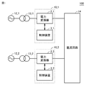
- FIG. 1 is a schematic configuration diagram of a power conversion system 100 according to the first embodiment.
- the power conversion system 100 is also collectively referred to as a power conversion device 10_1, 10_2 (hereinafter, also collectively referred to as “power conversion device 10”) and an AC system 12_1, 12_2 (hereinafter, also collectively referred to as “AC system 12”). ), Transformers 13_1, 13_2 (hereinafter collectively referred to as "transformer 13”), and a DC circuit 14.
- a configuration in which two systems including an AC system 12, a transformer 13, and a power conversion device 10 are connected to a common DC circuit 14 will be described. However, it may be configured such that three or more systems are connected to the DC circuit 14.
- the AC system 12_1 and the AC system 12_2 are three-phase AC systems having different system conditions. Specifically, the fundamental frequency F1 of the AC system 12_1 is higher than the fundamental frequency F2 of the AC system 12_2, and for example, the fundamental frequencies F1 and F2 are 60 Hz and 50 Hz, respectively.
- the DC circuit 14 is a DC line or a DC bus.
- the power converter 10_1 includes a power converter 2_1 that performs power conversion between the AC system 12_1 and the DC circuit 14, and a control device 3_1.
- the power converter 10_2 includes a power converter 2_2 that performs power conversion between the AC system 12_2 and the DC circuit 14, and a control device 3_2.
- the power converters 2_1 and 2_2 are configured by an MMC conversion type power converter.
- the control device 3_1 controls the operation of the power converter 2_1.
- the control device 3_2 controls the operation of the power converter 2_2.
- the power converters 2_1 and 2_2 are also collectively referred to as “power converter 2”, and the control devices 3_1 and 3_2 are also collectively referred to as “control device 3”.
- the transformer 13_1 is connected between the AC system 12_1 and the power converter 2_1.
- the transformer 13_2 is connected between the AC system 12_2 and the power converter 2_2.
- the power converter 2_1 When power is transmitted from the AC system 12_1 to the AC system 12_2, the power converter 2_1 operates as a forward converter (REC: Rectifier), and the power converter 2_1 operates as an inverse converter (INV: Inverter). Specifically, the AC power is converted into DC power by the power converter 2_1, and the converted DC power is transmitted to DC via the DC circuit 14. DC power is converted into AC power by the power converter 2_2 at the receiving end, and is supplied to the AC system 12_2 via the transformer 13_2.
- the power converter 2_1 operates as an inverse converter and the power converter 2_1 operates as a forward converter, the conversion operation opposite to the above is performed.
- FIG. 2 is a schematic configuration diagram of the power converter 2.
- the power converter 2 is composed of an MMC converter including a plurality of submodules (corresponding to “SM” in FIG. 2) 7 connected in series with each other.
- the power converter 2 has a plurality of leg circuits 4u, which are connected in parallel between the positive electrode DC terminal (that is, the high potential side DC terminal) Np and the negative electrode DC terminal (that is, the low potential side DC terminal) Nn.
- Includes 4v, 4w hereinafter, referred to as "leg circuit 4" when generically or arbitrarily indicated).
- the leg circuit 4 is provided in each of the plurality of phases constituting the alternating current.
- the leg circuit 4 is connected between the AC system 12 and the DC circuit 14, and performs power conversion between the two systems.
- the power converter 2 is provided with three leg circuits 4u, 4v, 4w corresponding to the U phase, the V phase, and the W phase, respectively.
- the AC input terminals Nu, Nv, Nw provided in the leg circuits 4u, 4v, 4w, respectively, are connected to the AC system 12 via the transformer 13.
- the connection between the AC input terminals Nv, Nw and the transformer 13 is not shown.
- the positive electrode DC terminal Np and the negative electrode DC terminal Nn commonly connected to each leg circuit 4 are connected to the DC circuit 14.
- the leg circuit 4u includes an upper arm 5 from the positive electrode DC terminal Np to the AC input terminal Nu, and a lower arm 6 from the negative electrode DC terminal Nn to the AC input terminal Nu.
- the AC input terminal Nu which is a connection point between the upper arm 5 and the lower arm 6, is connected to the transformer 13. Since the leg circuits 4v and 4w have the same configuration, the leg circuits 4u will be described below as a representative.
- the upper arm 5 includes a plurality of cascade-connected submodules 7 and a reactor 8A.
- the plurality of submodules 7 and the reactor 8A are connected in series with each other.
- the lower arm 6 includes a plurality of cascaded submodules 7 and a reactor 8B.
- the plurality of submodules 7 and the reactor 8B are connected in series with each other.
- the upper arm 5 and the lower arm 6 may be connected to the AC system 12 via a three-winding transformer having an impedance equivalent to that of the reactor instead of the reactor.
- the power conversion system 100 is provided with each detector that measures the amount of electricity used for control (for example, current, voltage, etc.).
- each detector is an AC voltage detector 18, an AC current detector 16, DC voltage detectors 11A, 11B, arm current detectors 9A, 9B provided in each leg circuit 4, and the like.
- the signal detected by these detectors is input to the control device 3.
- the control device 3 outputs an operation command for controlling the operation state of each submodule 7 in the power converter 2 based on these detection signals.
- the operation command is generated corresponding to each arm (for example, U-phase upper arm, U-phase lower arm, V-phase upper arm, V-phase lower arm, W-phase upper arm, and W-phase lower arm).
- the control device 3 receives various information from each submodule 7.
- the various information is internal information of the sub-module 7, and includes the voltage value of the capacitor of the sub-module 7, the state information indicating the state of the sub-module 7, and the like.
- the state information includes information indicating whether the submodule 7 is in a normal operating state or a stopped state, information indicating whether or not the submodule 7 has failed, and the like.
- the control device 3 typically includes an auxiliary transformer, an AD (Analog to Digital) conversion unit, a calculation unit, and the like as a hardware configuration.
- the arithmetic unit includes a CPU (Central Processing Unit), a RAM (Random Access Memory), and a ROM (Read Only Memory).
- the AD conversion unit includes an analog filter, a sample hold circuit, a multiplexer and the like.
- the control device 3 may be composed of, for example, a digital protection control device.
- the signal line of the signal input from each detector to the control device 3 and the signal line of the signal input / output between the control device 3 and each submodule 7 are one. Although the parts are described collectively, they are actually provided for each detector and each submodule 7.
- the signal lines between each submodule 7 and the control device 3 may be provided separately for transmission and reception.
- the signal line is composed of, for example, an optical fiber.
- the AC voltage detector 18 detects the U-phase AC voltage Vacu, the V-phase AC voltage Vacv, and the W-phase AC voltage Vacw of the AC system 12.
- the AC current detector 16 detects the U-phase AC current Iacu, the V-phase AC current Iacv, and the W-phase AC current Iacw of the AC system 12.
- the DC voltage detector 11A detects the DC voltage Vdcp of the positive electrode DC terminal Np connected to the DC circuit 14.
- the DC voltage detector 11B detects the DC voltage Vdcn of the negative electrode DC terminal Nn connected to the DC circuit 14. The difference between the DC voltage Vdcp and the DC voltage Vdcn is defined as the DC voltage Vdc.
- the arm current detectors 9A and 9B provided in the leg circuit 4u for the U phase detect the arm current Ipu flowing in the upper arm 5 and the arm current Inu flowing in the lower arm 6, respectively.
- the arm current detectors 9A and 9B provided in the leg circuit 4v for the V phase detect the arm current Ipv and the arm current Inv, respectively.
- the arm current detectors 9A and 9B provided in the leg circuit 4w for the W phase detect the arm current Ipw and the arm current Inw, respectively.
- the arm currents Ipu, Inu, Ipv, Inv, Ipw, and Inw are collectively referred to as arm currents Iarm.
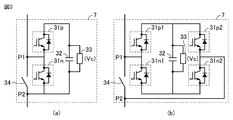
- FIG. 3 is a circuit diagram showing an example of a submodule.
- the sub-module 7 shown in FIG. 3A has a circuit configuration called a half-bridge configuration.
- the sub-module 7 includes a series body formed by connecting two switching elements 31p and 31n in series, a capacitor 32 as an energy storage device, a voltage detector 33, and a bypass switch 34.
- the series body and the capacitor 32 are connected in parallel.
- the voltage detector 33 detects the capacitor voltage Vc, which is the voltage across the capacitor 32.
- the submodule 7 shown in FIG. 3B has a circuit configuration called a full bridge configuration.
- the sub-module 7 includes a first series body formed by connecting two switching elements 31p1, 31n1 in series, and a second series body formed by connecting two switching elements 31p2, 31n2 in series. It includes a capacitor 32 and a voltage detector 33.
- the first series body, the second series body, and the capacitor 32 are connected in parallel.
- the voltage detector 33 detects the capacitor voltage Vc.
- the two switching elements 31p and 31n in FIG. 3A and the four switching elements 31p1, 31n1, 31p2 and 31n2 in FIG. 3B are, for example, an IGBT (Insulated Gate Bipolar Transistor) and a GCT (Gate Commutated Turn). -off) A freewheeling diode (FWD) is connected in anti-parallel to a self-extinguishing semiconductor switching element such as a thyristor or MOSFET (Metal Oxide Semiconductor Field-Effect Transistor). Further, in FIGS. 3A and 3B, a capacitor such as a film capacitor is mainly used as the capacitor 32.
- the switching elements 31p, 31n, 31p1, 31n1, 31p2, 31n2 are also collectively referred to as the switching element 31. Further, the on / off of the semiconductor switching element in the switching element 31 is simply referred to as “on / off of the switching element 31”.
- both terminals of the switching element 31n are designated as input / output terminals P1 and P2.
- the voltage across the capacitor 32 and the zero voltage are output by the switching operation of the switching elements 31p and 31n. For example, when the switching element 31p is turned on and the switching element 31n is turned off, the voltage across the capacitor 32 is output. A zero voltage is output when the switching element 31p is off and the switching element 31n is on.
- both terminals of the switching element 31n are input / output terminals P1 and P2, but both terminals of the switching element 31p may be input / output terminals P1 and P2, in which case the operation is reversed. ..
- the bypass switch 34 is connected between the input / output terminals P1 and P2.
- the bypass switch 34 is connected in parallel with the switching element 31n.
- the bypass switch 34 is connected in parallel with the switching element 31p.
- the bypass switch 34 is also used to short-circuit the sub-module 7 when each element of the sub-module 7 fails. As a result, even if any submodule 7 among the plurality of submodules 7 fails, the operation of the power converter 2 can be continued by using the other submodule 7.
- the midpoint between the switching element 31p1 and the switching element 31n1 and the midpoint between the switching element 31p2 and the switching element 31n2 are designated as the input / output terminals P1 and P2 of the submodule 7. do.
- the submodule 7 shown in FIG. 3B outputs a positive voltage or a zero voltage by constantly turning on the switching element 31n2, always turning off the switching element 31p2, and alternately turning on the switching elements 31p1 and 31n1. do.
- the submodule 7 shown in FIG. 3B has a zero voltage or a negative voltage by constantly turning off the switching element 31n2, constantly turning on the switching element 31p2, and alternately turning on the switching elements 31p1 and 31n1. Can also be output.
- the bypass switch 34 is connected between the input / output terminals P1 and P2.
- the bypass switch 34 is connected in parallel with a series of switching elements 31n1 and 31n2. By turning on the bypass switch 34, the submodule 7 is short-circuited.
- the sub-module 7 has the configuration of the half-bridge cell shown in FIG. 3A and a semiconductor switching element and a capacitor as an energy storage element are used will be described as an example.
- the sub-module 7 may have a full bridge configuration shown in FIG. 3 (b).
- a submodule other than the configuration shown above for example, a submodule to which a circuit configuration called a 1.5 half bridge configuration in which one of the switching elements 31 in FIG. 3B is replaced with only a diode is applied. May be used.
- the output DC voltage of the power converter 2 using the MMC converter is the DC voltage Vdc between the positive electrode DC terminal Np and the negative electrode DC terminal Nn.
- the DC voltage Vdc is determined by the sum of products of the instantaneous capacitor voltage Vcj of the jth submodule 7j constituting each leg circuit 4 and the switching state Si.
- the switching state Sj is assumed to be "1" when the switching element 31p is on and "0" when the switching element 31p is off.
- the time average voltage value Vav (hereinafter, also simply referred to as “average voltage value Vav”) is obtained by dividing the sum of the instantaneous capacitor voltages Vcj of each submodule 7j in the arm by the number of submodules n. , Expressed by the following equation (2).
- the symbol “ ⁇ >” in the equation (2) represents a time average.
- Vav ⁇ ( ⁇ Vcj) / n> ... (2)
- the control device 3 during the normal power conversion operation (that is, the normal operation), the time average voltage value of the capacitor voltage Vc of each submodule 7 in the arm becomes the value Vav represented by the equation (2). As such, each submodule 7 in the arm is controlled.
- FIG. 4 is a diagram for explaining the voltage fluctuation of the capacitor.
- the waveform 210 shows the time change of the capacitor voltage Vc1 of the capacitor 32 (hereinafter, also referred to as “capacitor 32_1”) mounted on the submodule 7 of the power converter 2_1.
- the waveform 220 shows the time change of the capacitor voltage Vc2 of the capacitor 32 (hereinafter, also referred to as “capacitor 32_2”) mounted on the submodule 7 of the power converter 2_2.
- Each capacitor 32_1 and 32_2 are composed of capacitors having the same rating (for example, the same capacitance, withstand voltage, etc.).
- the ripple voltage Vrp generated in the capacitor has the relationship as shown in the following equation (3), where C is the capacitance of the capacitor, F is the fundamental frequency, and Icap is the current flowing through the capacitor.
- the fundamental frequency F1 of the AC system 12_1 is 60 Hz
- the fundamental frequency F2 of the AC system 12_2 is 50 Hz. Therefore, the ripple voltage Vrp1 of the capacitor 32_1 in the power converter 2_1 connected to the AC system 12_1 is smaller than the ripple voltage Vrp2 of the capacitor 32_1 in the power converter 2_2 connected to the AC system 12_2.
- the ripple voltage Vrp1 is the difference between the maximum voltage value Vmax1 of the capacitor voltage Vc1 and the average voltage value Vav1.
- the ripple voltage Vrp2 is the difference between the maximum voltage value Vmax2 of the capacitor voltage Vc2 and the average voltage value Vav2.
- the capacitances of the capacitors 32_1 and 32_2 configured by the same component are the same. Assuming that the currents Icap are the same, the ripple voltage Vrp1 is 5/6 times the ripple voltage Vrp2.
- the difference value Vdi is used to adjust the average voltage value of the capacitor 32_1 to reduce the number of submodules included in the power converter 2_1 connected to the AC system 12_1 on the high frequency side. do. This reduces the size of the entire power conversion system.
- FIG. 5 is a diagram showing changes in the capacitor voltage according to the first embodiment.
- the average voltage value Vav1 * is larger than the average voltage value Vav2 by the difference value Vdi.
- the average voltage value Vav1 * is a value obtained by adding the difference value Vdi to the average voltage value Vav2.
- the average voltage value Vav of the capacitor changes according to the number of submodules n per arm.
- the rate of change of the average voltage value Vav1 * with respect to the average voltage value Vav1 of the capacitor 32_1 is X%, the following equation (4) is established.
- the number of submodules for each phase of the power converter 2_1 included in the power converter 10_1 is set to n1 *.
- the control device 3_1 is provided with each sub of the arm so that the time average voltage value of the capacitor voltage Vc of each submodule 7 included in the arm of the power converter 2_1 becomes the average voltage value Vav1 *.
- the number of submodules for each phase of the power converter 2_2 included in the power converter 10_2 is set to n2.
- the control device 3_2 has each sub in the arm so that the time average voltage value of the capacitor voltage Vc of each submodule 7 included in the arm of the power converter 2_2 becomes the average voltage value Vav2.
- Controls module 7. As a result, as shown in FIG. 5, the capacitor voltages Vc1 and Vc2 of the capacitors 32_1 and 32_2 change.
- the voltage margin Vg1 * of the capacitor 32_1 is the same as the voltage margin Vg2 of the capacitor 32_1. Become. Therefore, it is understood that the voltage margin Vg1 * of the capacitor 32_1 does not include an extra voltage margin while ensuring a voltage margin satisfying the specifications.
- the submodules 7 in the power converters 2_1 and 2_2 connected to the AC systems 12_1 and 12_2 having different basic frequencies are made the same, and the ripple voltage of the capacitors 32_1 and 32_2 generated thereby is the same.
- the number of submodules of the power converter 2_1 can be reduced by using the difference value Vdi of. Therefore, the size of the power converter 2_1 can be reduced while ensuring the maintainability of each power converter 2_1 and 2, and as a result, the size of the entire power conversion system can be reduced.
- the control device 3 receives the soundness determination signal indicating the soundness state of the submodule 7 as the state information of each submodule 7.
- the soundness determination signal is “1”
- the sub-module 7 is in a faulty state
- the soundness determination signal is “0”.
- the failure of the sub-module 7 is not limited to the element failure, and the sub-module 7 does not operate as instructed by the control device 3.
- the failure of the sub-module 7 includes a failure of a switching element, a failure of a gate driver, a failure of a capacitor, a damage of a bus bar, a communication abnormality, and the like.
- the control device 3 outputs an operation command corresponding to each arm (for example, U phase upper arm, U phase lower arm, V phase upper arm, V phase lower arm, W phase upper arm, and W phase lower arm). Controls each arm. Therefore, the control device 3 performs various controls for troubleshooting the arm including the failed sub-module 7.
- the number of submodules in the U-phase leg circuit 4u is 2 m (where m is an integer of 2 or more), the number of submodules of the U-phase upper arm is m, and the number of submodules of the U-phase lower arm.
- m is an integer of 2 or more
- the number of submodules of the U-phase upper arm is m
- the number of submodules of the U-phase lower arm Let be m pieces.
- the control device 3 among the m submodules 7 of the U-phase upper arm, the soundness determination signal received from k (where k is an integer of 1 or more and k ⁇ m) submodules 7_i is received. If it is "0", a failure of each submodule 7_i is detected.
- the control device 3 bypasses each submodule 7_i in which a failure has occurred by turning on the bypass switch 34 of each submodule 7_i.
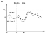
- FIG. 6 is a diagram showing changes in the capacitor voltage before and after an AC system accident.
- the waveform 250 shows the average voltage value Vav1 * of the capacitor 32_1.
- the average voltage value Vav1 * before the occurrence of the accident is described as “V0” for convenience.
- the average voltage value V0 is the same as the average voltage value Vav1 * in FIG.
- the waveform 260 shows the capacitor voltage Vc1 including the voltage fluctuation component of the capacitor 32_1 (that is, the ripple voltage Vrp1).
- An accident in the AC system 12_1 occurs at time t1, and the control device 3_1 detects the accident. For example, in the control device 3_1, when at least one of the absolute values of the arm currents Ipu, Ipv, Ipw, Inu, Inv, and Inw detected by the arm current detectors 9A and 9B exceeds the threshold Th1 or the arm When the total value of each phase of the current exceeds the threshold value Th2, it is determined that an accident has occurred in the AC system 12_1. Further, the control device 3_1 may determine that an accident has occurred when any of the AC voltages detected by the AC voltage detector 18 exceeds (or falls below) the threshold value Th3.
- the control device 3_1 controls each submodule 7 so that the time average voltage value of the capacitor voltage Vc of each submodule 7 in the arm becomes the average voltage value V0 from the time t0 to the time t1. .. However, when the control device 3_1 detects an accident at time t1, the time average voltage value of the capacitor voltage Vc of each submodule 7 in the arm is a value obtained by subtracting the reference value D1 from the average voltage value V0 (that is, V0-D1). ), Each submodule 7 is controlled. As a result, the control device 3_1 lowers the average voltage value Vav1 *.
- the control device 3_2 executes the same operation as the control device 3_1 described above. Specifically, when the control device 3_2 detects an accident in the AC system 12_2, the time average voltage value of the capacitor voltage Vc of each submodule 7 in the arm subtracts the reference value D2 from the average voltage value before the accident occurs. Each submodule 7 is controlled so as to have the specified value.
- the reference value D2 may be the same as the reference value D1. As a result, the control device 3_2 lowers the average voltage value Vav2.
- the control device 3_2 may lower the average voltage value Vav2.
- the control device 3_1 receives information from the control device 3_1 (or another higher-level device) indicating that an accident has occurred in the AC system 12_1. After receiving the information, the control device 3_2 lowers the average voltage value Vav2. Thereby, even if the accident of the AC system 12_1 may affect the capacitor voltage Vc2 of the submodule 7 in the power converter 2_2, the situation where the capacitor voltage Vc2 exceeds the withstand voltage V Albanyv can be prevented.
- Transformers 13_1 and 13_2 are transformers with variable transformation ratios.
- a transformer with a variable transformation ratio is realized, for example, by a transformer with a tap switching function.
- the control device 3 is configured to be communicable with the transformer 13, and transmits various commands such as an instruction to change the transformer ratio to the transformer 13.
- the system operator determines that the dielectric strength of the DC circuit 14 has decreased, the system operator inputs information indicating the decrease in the dielectric strength of the DC circuit 14 to the control devices 3_1 and 3_2.
- the DC voltage Vdc of the DC circuit 14 is lowered by ⁇ Vdc.
- the control device 3_1 lowers the average voltage value Vav1 * of the capacitor 32_1 in the submodule 7 included in the power converter 2_1 by ⁇ Vav1 *.
- the AC voltage on the primary side (that is, the AC system 12_1 side) of the transformer 13_1 is defined as V1_1.
- the AC voltage on the secondary side of the transformer 13_1 (that is, the power converter 2_1 side) before the decrease of the DC voltage Vdc is V2_1
- the AC voltage on the secondary side of the transformer 13_1 after the decrease is V2_1 *. ..
- the control device 3_1 adjusts the transformer ratio ⁇ 1 of the transformer 13_1 so that the AC voltage V1_1 on the primary side of the transformer 13_1 is maintained. Specifically, the control device 3_1 instructs the transformer 13_1 to change the transformation ratio ⁇ 1 from (V2_1) / (V1_1) to (V2_1 *) / (V1_1).
- the AC voltage on the primary side (that is, the AC system 12_2 side) of the transformer 13_2 is set to V1-2
- the control device 3_2 adjusts the transformation ratio ⁇ 2 of the transformer 13_2 so that the AC voltage V1_2 on the primary side of the transformer 13_2 is maintained.
- the control device 3_2 instructs the transformer 13_2 to change the transformation ratio ⁇ 2 from (V2_2) / (V1_2) to (V2_2 *) / (V1_2).
- Embodiment 2 In the first embodiment, the case where the fundamental frequencies of the plurality of AC systems 12_1 and 12_2 are different from each other has been described. In the second embodiment, a case where the power demands from the plurality of AC systems 12_1 and 12_2 are different from each other will be described.
- the ripple voltage increases in proportion to the current Icap flowing through the capacitor. Since the capacitances of the capacitors 32_1 and 32_2 made of the same component are the same, when the fundamental frequency F1 of the AC system 12_1 and the fundamental frequency F2 of the AC system 12_2 are the same, the larger the current Icap, the more ripple.
- the voltage Vrp increases.
- attention is paid to the difference in the current Icap flowing through the capacitor in the power converter 2_1, _2 caused by the difference in the power demand from the AC system 12_1, 12_1.
- the power converters 2_1 and 2_2 operate so as to satisfy the power demand from the AC system 12_1 and 12_2, respectively.
- the arm current Iarm flowing in the power converter 2 flows to the positive electrode side (that is, the switching element 31p side) and the negative electrode side (that is, the switching element 31n side) of the submodule 7, respectively.
- the semiconductor switching elements of the switching elements 31p and 31n will be described as being the IGBT.
- the current Isp flowing on the positive electrode side is the sum of the current flowing in the IGBT of the switching element 31p and the current flowing in the FWD of the switching element 31p. This added current becomes the current Icap flowing through the capacitor 32.
- the current Isn flowing on the negative electrode side is an additional current of the current flowing in the IGBT of the switching element 31n and the current flowing in the FWD of the switching element 31n. In the switching elements 31p and 31n, the current flowing through the FWD flows in the direction opposite to that of the IGBT.
- the current sharing ratio between the current Isp (that is, the current Icap) and the current Isn changes depending on the power factor (PF) of the AC system 12.
- the positive direction of the current Isp corresponds to the direction from the input / output terminal P1 to the switching element 31p1 in FIG. 3, and the positive direction of the current Isn corresponds to the direction from the input / output terminal P1 to the switching element 31n1.
- FIG. 7 is a diagram for explaining the relationship between the current Isp flowing on the positive electrode side and the current Isn flowing on the negative electrode side in the submodule.
- the straight lines 304, 306, and 308 are straight lines showing the relationship between the current Isp and the current Isn when the power factor of the AC system 12 is 0,0.95,1.00, respectively.
- the curve 362 shows each point where the current effective value of the arm current Iarm is the same.
- the larger the power factor at the AC output of the power converter 2 the more the current flows biased toward the negative electrode side, the larger the current Isn, and the smaller the current Isp.
- the smaller the power factor the larger the current Isp (that is, the current Icap).
- the larger the arm current Iarm the larger the current Icap. Since the magnitude of the arm current Iarm is proportional to the magnitude of the apparent power input / output between the power converter 2 and the AC system 12, it is input / output when the power factor is constant. It can be said that the larger the apparent power, the larger the current Icap.
- the magnitude of the current Icap is one of the input apparent power and the output apparent power. It depends on the larger apparent power.
- the magnitude of the current Icap flowing through the capacitors 32 in the power converters 2_1 and 2_2 is different, and as a result.
- the magnitude of the ripple voltage of the capacitor 32 will be different.
- the power factor required from the AC system 12_1 and the power factor required from the AC system 12_2 are the same.
- the input / output of the apparent power required from the AC system 12_1 is smaller than the input / output of the apparent power required from the AC system 12_1
- the current Icap1 flowing through the capacitor 32_1 in the power converter 2_1 Is smaller than the current Icap2 flowing through the capacitor 32_2 in the power converter 2_2.
- the input / output of the apparent power required from the AC system 12_1 is the same as the input / output of the apparent power required from the AC system 12_2.
- the current Icap1 flowing through the capacitor 32_1 in the power converter 2_1 converts the power. It is smaller than the current Icap2 flowing through the capacitor 32_2 in the vessel 2_2. Therefore, the ripple voltage Vrp1 of the capacitor 32_1 is smaller than the ripple voltage Vrp2 of the capacitor 32_1. Therefore, the number of submodules of the power converter 2_1 can be reduced by increasing the average voltage value of the capacitor voltage Vc1 of the capacitor 32_1 by the difference value Vdi from the average voltage value of the capacitor voltage Vc2 of the capacitor 32_1.
- the power factor required by the AC system 12_1 is smaller than the power factor required by the AC system 12_2, and the input / output of apparent power required by the AC system 12_1 Is smaller than the input / output of apparent power required from the AC system 12_2.
- the current Icap1 at the point 371 is smaller than the current Icap2 at the point 372. Therefore, the ripple voltage Vrp1 of the capacitor 32_1 is smaller than the ripple voltage Vrp2 of the capacitor 32_1. Therefore, the number of submodules of the power converter 2_1 can be reduced by increasing the average voltage value of the capacitor voltage Vc1 of the capacitor 32_1 by the difference value Vdi from the average voltage value of the capacitor voltage Vc2 of the capacitor 32_1.
- the effective value of the current that is, the current Icap1 of the capacitor 32_1 in the power converter 2_1 based on the power factor and the apparent power required from the AC system 12_1, and the power factor required from the AC system 12_2.
- the effective value of the current ie, current Icap2 of the capacitor 32_2 in the power converter 2_2 based on the apparent power is compared. Then, for example, when the current Icap1 is smaller than the current Icap2, the ripple voltage Vrp1 is smaller than the ripple voltage Vrp2, so that the number of submodules of the power converter 2_1 can be reduced.
- the submodules 7 in the power converters 2_1 and 2_2 connected to the AC systems 12_1 and 12_2 having different power requirements are made the same, and the difference value Vdi of the ripple voltage of the capacitors 32_1 and 32_2 generated by the submodules 7 is used. Therefore, the number of submodules of the power converter 2_1 can be reduced. Therefore, also in the second embodiment, the size of one of the power converters can be reduced while ensuring the maintainability of the power converters 2_1 and 2, and as a result, the size of the entire power conversion system can be reduced.
- the method of adjusting the average voltage value Vav in each of ⁇ when the submodule fails>, ⁇ when an AC system accident occurs>, and ⁇ when the dielectric strength of the DC circuit decreases> has been described.
- the method of adjusting the average voltage value Vav in each case can be adopted.
- the configuration exemplified as the above-described embodiment is an example of the configuration of the present disclosure, and can be combined with another known technique, and a part thereof may be omitted without departing from the gist of the present disclosure. , Can be modified and configured. Further, in the above-described embodiment, the processing and configuration described in the other embodiments may be appropriately adopted and carried out.
Landscapes
- Engineering & Computer Science (AREA)
- Power Engineering (AREA)
- Inverter Devices (AREA)
Abstract
電力変換システム(100)は、第1交流系統(12_1)と直流回路(14)との間で電力変換を行なう第1電力変換器(2_1)と、第2交流系統(12_2)と直流回路(14)との間で電力変換を行なう第2電力変換器(2_2)とを備える。第1電力変換器(2_1)および第2電力変換器(2_2)の各々は、直列接続された複数のサブモジュール(7)を含む。サブモジュール(7)は、複数のスイッチング素子(31)と、コンデンサ(32)とを有する。第1交流系統(12_1)の第1基本周波数は、第2交流系統(12_2)の第2基本周波数よりも大きい。第1電力変換器(2_1)に含まれる第1サブモジュール(7)内のコンデンサ(32)の第1平均電圧値は、第2電力変換器(2_2)に含まれる第2サブモジュール(7)内のコンデンサ(32)の第2平均電圧値よりも大きい。
Description
本開示は、電力変換システムに関する。
複数の単位変換器がカスケード接続されるモジュラーマルチレベル変換器(以下、MMC変換器とも称する。)は、単位変換器の数を増加させることによって、高電圧化に容易に対応することができる。「単位変換器」は、「サブモジュール(sub module)」あるいは「変換器セル」とも称される。MMC変換器は、大容量の静止型無効電力補償装置、または高圧直流送電用の電力変換装置として、送配電系統へ広く適用されている。
特開2012-228025号公報(特許文献1)では、電源側、または負荷側電圧の基本周波数の周期による直流コンデンサ電圧の変動を抑制することを検討している。
MMC方式の電力変換器を含む電力変換システムは、例えば、直流送電系統の電力を制御するためのシステムとして用いられる。典型的には、直流回路を介して2つの交流系統間で電力授受が行われるが、これらの交流系統の系統条件(例えば、基本周波数、電力要求)が異なる場合がある。この場合、一方の交流系統に接続される電力変換器と、他方の交流系統に接続される電力変換器とでは必要とされる仕様が異なる。しかし、保守性の観点から両者の電力変換器には、同一の部品(例えば、直流コンデンサ)で構成されるサブモジュールを用いることが好ましい。
例えば、両者の交流系統における基本周波数が異なる場合、基本周波数が低い交流系統側における第1直流コンデンサの電圧変動は、基本周波数が高い交流系統側における第2直流コンデンサの電圧変動よりも大きい。そのため、第2直流コンデンサの電圧変動の抑制に必要な静電容量は、第1直流コンデンサの電圧変動の抑制に必要な静電容量よりも小さい。したがって、両者で同一の直流コンデンサを用いる場合には、第1直流コンデンサの電圧変動の抑制に必要な静電容量を採用する必要がある。この場合、第2直流コンデンサの電圧変動は、求められた仕様よりも大きく抑制されるため、最大電圧と耐電圧との偏差(すなわち、マージン)が大きくなってしまい無駄が生じる。特許文献1では、このような課題に対する解決策を何ら教示または示唆するものではない。
本開示のある局面における目的は、系統条件が異なる複数の交流系統にそれぞれ接続される複数の電力変換器の保守性を確保しつつ、システム全体のサイズを小さくすることが可能な電力変換システムを提供することである。
ある実施の形態に従う電力変換システムは、第1交流系統と直流回路との間で電力変換を行なう第1電力変換器と、第2交流系統と直流回路との間で電力変換を行なう第2電力変換器とを備える。第1電力変換器および第2電力変換器の各々は、直列接続された複数のサブモジュールを含む。サブモジュールは、複数のスイッチング素子と、コンデンサとを有する。第1交流系統の第1基本周波数は、第2交流系統の第2基本周波数よりも大きい。第1電力変換器に含まれる第1サブモジュール内のコンデンサの第1平均電圧値は、第2電力変換器に含まれる第2サブモジュール内のコンデンサの第2平均電圧値よりも大きい。
他の実施の形態に従う電力変換システムは、第1交流系統と直流回路との間で電力変換を行なう第1電力変換器と、第2交流系統と直流回路との間で電力変換を行なう第2電力変換器とを備える。第1電力変換器および第2電力変換器の各々は、直列接続された複数のサブモジュールを含む。サブモジュールは、複数のスイッチング素子と、コンデンサとを有する。第1交流系統から要求される力率および皮相電力に基づく、第1電力変換器に含まれる第1サブモジュール内のコンデンサの電流実効値は、第2交流系統から要求される力率および皮相電力に基づく、第2電力変換器に含まれる第2サブモジュール内のコンデンサの電流実効値よりも小さい。第1サブモジュール内のコンデンサの第1平均電圧値は、第2サブモジュール内のコンデンサの第2平均電圧値よりも大きい。
本開示によると、電力変換システムにおいて、系統条件が異なる複数の交流系統にそれぞれ接続される複数の電力変換器の保守性を確保しつつ、システム全体のサイズを小さくすることができる。
以下、図面を参照しつつ、本実施の形態について説明する。以下の説明では、同一の部品には同一の符号を付してある。それらの名称および機能も同じである。したがって、それらについての詳細な説明は繰り返さない。
実施の形態1.
<システムの全体構成>
図1は、実施の形態1に従う電力変換システム100の概略構成図である。図1を参照して、電力変換システム100は、電力変換装置10_1,10_2(以下「電力変換装置10」とも総称する。)と、交流系統12_1,12_2(以下「交流系統12」とも総称する。)と、変圧器13_1,13_2(以下「変圧器13」とも総称する。)と、直流回路14とを含む。以下では、交流系統12、変圧器13および電力変換装置10を含むシステムが共通の直流回路14に2つ接続される構成について説明する。しかし、3つ以上のシステムが直流回路14に接続される構成であってもよい。
<システムの全体構成>
図1は、実施の形態1に従う電力変換システム100の概略構成図である。図1を参照して、電力変換システム100は、電力変換装置10_1,10_2(以下「電力変換装置10」とも総称する。)と、交流系統12_1,12_2(以下「交流系統12」とも総称する。)と、変圧器13_1,13_2(以下「変圧器13」とも総称する。)と、直流回路14とを含む。以下では、交流系統12、変圧器13および電力変換装置10を含むシステムが共通の直流回路14に2つ接続される構成について説明する。しかし、3つ以上のシステムが直流回路14に接続される構成であってもよい。
電力変換システム100では、直流回路14を介して、交流系統12_1と交流系統12_2間で電力が送受される。交流系統12_1と交流系統12_2とは系統条件が互いに異なる3相交流系統である。具体的には、交流系統12_1の基本周波数F1は、交流系統12_2の基本周波数F2よりも高く、例えば、基本周波数F1,F2は、それぞれ60Hz,50Hzである。直流回路14は、直流線路または直流バスである。
電力変換装置10_1は、交流系統12_1と直流回路14との間で電力変換を行なう電力変換器2_1と、制御装置3_1とを含む。電力変換装置10_2は、交流系統12_2と直流回路14との間で電力変換を行なう電力変換器2_2と、制御装置3_2とを含む。電力変換器2_1,2_2は、MMC変換方式の電力変換器によって構成される。制御装置3_1は、電力変換器2_1の動作を制御する。制御装置3_2は、電力変換器2_2の動作を制御する。以下の説明では、電力変換器2_1,2_2を「電力変換器2」とも総称し、制御装置3_1,3_2を「制御装置3」とも総称する。
変圧器13_1は、交流系統12_1と電力変換器2_1との間に接続される。変圧器13_2は、交流系統12_2と電力変換器2_2との間に接続される。
交流系統12_1から交流系統12_2に電力が送電される場合、電力変換器2_1は順変換器(REC:Rectifier)として動作し、電力変換器2_2は逆変換器(INV:Inverter)として動作する。具体的には、電力変換器2_1により交流電力が直流電力に変換され、この変換された直流電力が直流回路14を介して直流送電される。受電端において電力変換器2_2により直流電力が交流電力に変換され、変圧器13_2を介して交流系統12_2に供給される。電力変換器2_2が逆変換器として動作し、電力変換器2_1が順変換器として動作する場合には、上記と逆の変換動作が行われる。
<電力変換装置の構成>
図2は、電力変換器2の概略構成図である。図2を参照して、電力変換器2は、互いに直列接続された複数のサブモジュール(図2中の「SM」に対応)7を含むMMC変換器によって構成されている。
図2は、電力変換器2の概略構成図である。図2を参照して、電力変換器2は、互いに直列接続された複数のサブモジュール(図2中の「SM」に対応)7を含むMMC変換器によって構成されている。
電力変換器2は、正極直流端子(すなわち、高電位側直流端子)Npと、負極直流端子(すなわち、低電位側直流端子)Nnとの間に互いに並列に接続された複数のレグ回路4u,4v,4w(以下、総称する場合または任意のものを示す場合、「レグ回路4」と記載する)を含む。
レグ回路4は、交流を構成する複数相の各々に設けられる。レグ回路4は、交流系統12と直流回路14との間に接続され、両系統間で電力変換を行なう。電力変換器2には、U相、V相、W相にそれぞれ対応して3個のレグ回路4u,4v,4wが設けられる。
レグ回路4u,4v,4wにそれぞれ設けられた交流入力端子Nu,Nv,Nwは、変圧器13を介して交流系統12に接続される。図2では、図解を容易にするために、交流入力端子Nv,Nwと変圧器13との接続は図示されていない。各レグ回路4に共通に接続された正極直流端子Npおよび負極直流端子Nnは、直流回路14に接続される。
レグ回路4uは、正極直流端子Npから交流入力端子Nuまでの上アーム5と、負極直流端子Nnから交流入力端子Nuまでの下アーム6とを含む。上アーム5と下アーム6との接続点である交流入力端子Nuが変圧器13と接続される。レグ回路4v,4wについても同様の構成を有するので、以下、レグ回路4uを代表として説明する。
上アーム5は、カスケード接続された複数のサブモジュール7と、リアクトル8Aとを含む。当該複数のサブモジュール7およびリアクトル8Aは互いに直列接続されている。下アーム6は、カスケード接続された複数のサブモジュール7と、リアクトル8Bとを含む。当該複数のサブモジュール7およびリアクトル8Bは互いに直列接続されている。なお、上アーム5および下アーム6は、リアクトルの代わりに、リアクトル相当のインピーダンスを有する3巻線変圧器を介して交流系統12と接続されていてもよい。
電力変換システム100には、制御に使用される電気量(例えば、電流、電圧など)を計測する各検出器が設けられている。例えば、各検出器は、交流電圧検出器18、交流電流検出器16、直流電圧検出器11A,11B、各レグ回路4に設けられたアーム電流検出器9A,9B等である。これらの検出器によって検出された信号は、制御装置3に入力される。
制御装置3は、これらの検出信号に基づいて電力変換器2内の各サブモジュール7の運転状態を制御するための運転指令を出力する。運転指令は、各アーム(例えば、U相上アーム、U相下アーム、V相上アーム、V相下アーム、W相上アーム、およびW相下アーム)にそれぞれ対応して生成される。また、制御装置3は、各サブモジュール7から各種情報を受信する。各種情報は、サブモジュール7の内部情報であり、サブモジュール7のコンデンサの電圧値、サブモジュール7の状態を示す状態情報等を含む。状態情報は、サブモジュール7が通常動作している通常動作状態か、停止状態かを示す情報、サブモジュール7の故障の有無を示す情報等を含む。
制御装置3は、典型的には、ハードウェア構成として、補助変成器、AD(Analog to Digital)変換部、演算部等を含む。演算部は、CPU(Central Processing Unit)、RAM(Random Access Memory)およびROM(Read Only Memory)を含む。AD変換部は、アナログフィルタ、サンプルホールド回路、マルチプレクサ等を含む。制御装置3は、例えば、ディジタル保護制御装置で構成されていてもよい。
図1では図解を容易にするために、各検出器から制御装置3に入力される信号の信号線と、制御装置3および各サブモジュール7間で入出力される信号の信号線とは、一部まとめて記載されているが、実際には検出器ごとおよびサブモジュール7ごとに設けられている。各サブモジュール7と制御装置3との間の信号線は、送信用と受信用とが別個に設けられていてもよい。信号線は、たとえば光ファイバによって構成される。
交流電圧検出器18は、交流系統12のU相の交流電圧Vacu、V相の交流電圧Vacv、およびW相の交流電圧Vacwを検出する。交流電流検出器16は、交流系統12のU相の交流電流Iacu、V相の交流電流Iacv、およびW相の交流電流Iacwを検出する。直流電圧検出器11Aは、直流回路14に接続された正極直流端子Npの直流電圧Vdcpを検出する。直流電圧検出器11Bは、直流回路14に接続された負極直流端子Nnの直流電圧Vdcnを検出する。直流電圧Vdcpと直流電圧Vdcnとの差を直流電圧Vdcとする。
U相用のレグ回路4uに設けられたアーム電流検出器9Aおよび9Bは、上アーム5に流れるアーム電流Ipuおよび下アーム6に流れるアーム電流Inuをそれぞれ検出する。同様に、V相用のレグ回路4vに設けられたアーム電流検出器9Aおよび9Bは、アーム電流Ipvおよびアーム電流Invをそれぞれ検出する。W相用のレグ回路4wに設けられたアーム電流検出器9Aおよび9Bは、アーム電流Ipwおよびアーム電流Inwをそれぞれ検出する。以下の説明では、アーム電流Ipu,Inu,Ipv,Inv,Ipw,Inwを総称してアーム電流Iarmと記載する。
<サブモジュールの構成>
図3は、サブモジュールの一例を示す回路図である。図3(a)に示すサブモジュール7は、ハーフブリッジ構成と呼ばれる回路構成を有する。このサブモジュール7は、2つのスイッチング素子31p、31nを直列接続して形成した直列体と、エネルギー蓄積器としてのコンデンサ32と、電圧検出器33と、バイパススイッチ34とを含む。直列体とコンデンサ32とは並列接続される。電圧検出器33は、コンデンサ32の両端の電圧であるコンデンサ電圧Vcを検出する。
図3は、サブモジュールの一例を示す回路図である。図3(a)に示すサブモジュール7は、ハーフブリッジ構成と呼ばれる回路構成を有する。このサブモジュール7は、2つのスイッチング素子31p、31nを直列接続して形成した直列体と、エネルギー蓄積器としてのコンデンサ32と、電圧検出器33と、バイパススイッチ34とを含む。直列体とコンデンサ32とは並列接続される。電圧検出器33は、コンデンサ32の両端の電圧であるコンデンサ電圧Vcを検出する。
図3(b)に示すサブモジュール7は、フルブリッジ構成と呼ばれる回路構成を有する。このサブモジュール7は、2つのスイッチング素子31p1,31n1を直列接続して形成された第1の直列体と、2つのスイッチング素子31p2,31n2を直列接続して形成された第2の直列体と、コンデンサ32と、電圧検出器33とを含む。第1の直列体と、第2の直列体と、コンデンサ32とが並列接続される。電圧検出器33は、コンデンサ電圧Vcを検出する。
図3(a)における2つのスイッチング素子31p、31nと、図3(b)における4つのスイッチング素子31p1、31n1、31p2、31n2とは、例えば、IGBT(Insulated Gate Bipolar Transistor)、GCT(Gate Commutated Turn-off)サイリスタ、MOSFET(Metal Oxide Semiconductor Field-Effect Transistor)などの自己消弧型の半導体スイッチング素子に還流ダイオード(FWD:Freewheeling Diode)が逆並列に接続されて構成される。また、図3(a)および図3(b)において、コンデンサ32には、フィルムコンデンサなどのキャパシタが主に用いられる。
以下の説明では、スイッチング素子31p,31n,31p1,31n1,31p2,31n2をスイッチング素子31とも総称する。また、スイッチング素子31内の半導体スイッチング素子のオンオフを、単に「スイッチング素子31のオンオフ」と記載する。
図3(a)を参照して、スイッチング素子31nの両端子を入出力端子P1,P2とする。スイッチング素子31p、31nのスイッチング動作によりコンデンサ32の両端電圧、および零電圧を出力する。例えば、スイッチング素子31pがオン、かつスイッチング素子31nがオフとなったときに、コンデンサ32の両端電圧が出力される。スイッチング素子31pがオフ、かつスイッチング素子31nがオンとなったときに、零電圧が出力される。図3(a)では、スイッチング素子31nの両端子を入出力端子P1,P2としたが、スイッチング素子31pの両端子を入出力端子P1,P2としてもよく、その場合には、動作が反転する。
バイパススイッチ34は、入出力端子P1,P2間に接続される。図3(a)では、バイパススイッチ34は、スイッチング素子31nと並列に接続される。ただし、スイッチング素子31pの両端子を入出力端子P1,P2とする場合には、バイパススイッチ34は、スイッチング素子31pと並列に接続される。バイパススイッチ34をオンにすることによって、サブモジュール7が短絡される。バイパススイッチ34は、サブモジュール7の各素子が故障した場合に、当該サブモジュール7を短絡させる際にも利用される。これにより、複数のサブモジュール7のうちの任意のサブモジュール7が故障しても、他のサブモジュール7を利用することにより電力変換器2の運転継続が可能となる。
次に、図3(b)を参照して、スイッチング素子31p1とスイッチング素子31n1との中点と、スイッチング素子31p2とスイッチング素子31n2との中点とをサブモジュール7の入出力端子P1,P2とする。図3(b)に示すサブモジュール7は、スイッチング素子31n2を常時オンとし、スイッチング素子31p2を常時オフとし、スイッチング素子31p1,31n1を交互にオン状態とすることによって、正電圧または零電圧を出力する。また、図3(b)に示すサブモジュール7は、スイッチング素子31n2を常時オフし、スイッチング素子31p2を常時オンし、スイッチング素子31p1,31n1を交互にオン状態にすることによって、零電圧または負電圧を出力することもできる。
バイパススイッチ34は、入出力端子P1,P2間に接続される。なお、バイパススイッチ34は、スイッチング素子31n1,31n2の直列体と並列に接続される。バイパススイッチ34をオンにすることによって、サブモジュール7が短絡される。
以下の説明では、サブモジュール7を図3(a)に示すハーフブリッジセルの構成とし、半導体スイッチング素子、およびエネルギー蓄積要素としてのコンデンサを用いた場合を例に説明する。しかし、サブモジュール7を図3(b)に示すフルブリッジ構成としてもよい。また、上記で示した構成以外のサブモジュール、例えば、図3(b)の各スイッチング素子31のうちの1つをダイオードのみで置き換えた1.5ハーフブリッジ構成とも呼ばれる回路構成を適用したサブモジュールを用いてもよい。
<サブモジュールのコンデンサ電圧>
MMC変換器を用いた電力変換器2の出力直流電圧は、正極直流端子Npと負極直流端子Nnとの間の直流電圧Vdcである。直流電圧Vdcは、各レグ回路4を構成しているj番目のサブモジュール7jの瞬時のコンデンサ電圧Vcjと、スイッチング状態Siとの積和で決定される。スイッチング状態Sjは、スイッチング素子31pがオンの場合には“1”、スイッチング素子31pがオフの場合には“0”であるとする。
MMC変換器を用いた電力変換器2の出力直流電圧は、正極直流端子Npと負極直流端子Nnとの間の直流電圧Vdcである。直流電圧Vdcは、各レグ回路4を構成しているj番目のサブモジュール7jの瞬時のコンデンサ電圧Vcjと、スイッチング状態Siとの積和で決定される。スイッチング状態Sjは、スイッチング素子31pがオンの場合には“1”、スイッチング素子31pがオフの場合には“0”であるとする。
ここで、説明の容易化のため、アーム間およびアーム内での各サブモジュール7のコンデンサ電圧Vcのバラツキは無視するものとする。コンデンサ電圧Vcの時間平均電圧値をVav、直流変調率をMdc、アームあたりの(すなわち、各アームに含まれる)サブモジュール数をnとすると、以下の式(1)が成立する。この場合、各レグ回路4に含まれるサブモジュール数は2nとなる。
Vdc=Σ(Vcj×Sj)=Vav×2n×Mdc …(1)
上述した式(1)より、直流変調率Mdcを一定(典型的には、0.5)にするとサブモジュール数nは、Vdc/Vavに比例するため、平均電圧値Vavを大きくするとサブモジュール数nを削減できる。
上述した式(1)より、直流変調率Mdcを一定(典型的には、0.5)にするとサブモジュール数nは、Vdc/Vavに比例するため、平均電圧値Vavを大きくするとサブモジュール数nを削減できる。
なお、時間平均電圧値Vav(以下、単に「平均電圧値Vav」とも称する。)は、アーム内の各サブモジュール7jの瞬時のコンデンサ電圧Vcjの総和をサブモジュール数nで除算することにより求められ、以下の式(2)で表される。式(2)中の記号“<>”は、時間平均を表わしている。
Vav=<(ΣVcj)/n> …(2)
制御装置3は、通常の電力変換動作(すなわち、通常動作)の際には、アーム内の各サブモジュール7のコンデンサ電圧Vcの時間平均電圧値が、式(2)で示される値Vavとなるように、当該アーム内の各サブモジュール7を制御する。
制御装置3は、通常の電力変換動作(すなわち、通常動作)の際には、アーム内の各サブモジュール7のコンデンサ電圧Vcの時間平均電圧値が、式(2)で示される値Vavとなるように、当該アーム内の各サブモジュール7を制御する。
しかしながら、電力変換器2では、サブモジュール7に搭載されたコンデンサ32に基本周波数成分が主体の交流成分を有する電流が流れ込むため、実際にはコンデンサ32においてリップル電圧が生じ、コンデンサ電圧Vcは平均電圧値Vavを中心に変動する。
図4は、コンデンサの電圧変動を説明するための図である。図4を参照して、波形210は、電力変換器2_1のサブモジュール7に搭載されたコンデンサ32(以下「コンデンサ32_1」とも称する。)のコンデンサ電圧Vc1の時間変化を示している。波形220は、電力変換器2_2のサブモジュール7に搭載されたコンデンサ32(以下「コンデンサ32_2」とも称する。)のコンデンサ電圧Vc2の時間変化を示している。なお、各コンデンサ32_1,32_2は、同一定格(例えば、静電容量、耐圧等が同一)のコンデンサで構成される。
図4の例では、電力変換器2_1の各アームに含まれるサブモジュール数n1と、電力変換器2_2の各アームに含まれるサブモジュール数n2とは同一であるとする。また、電力変換器2_1と電力変換器2_2とは共通の直流回路14に接続されている。そのため、式(1)より、コンデンサ電圧Vc1の平均電圧値Vav1と、コンデンサ電圧Vc2の平均電圧値Vav2とは同一となる。
ここで、コンデンサに生じるリップル電圧Vrpは、コンデンサの静電容量をC、基本周波数をF、コンデンサに流れる電流をIcapとすると、以下の式(3)のような関係を有する。
Vrp∝(1/C)×(1/F)×Icap …(3)
実施の形態1では、交流系統12_1の基本周波数F1が60Hzであり、交流系統12_2の基本周波数F2が50Hzである。そのため、交流系統12_1に接続された電力変換器2_1内のコンデンサ32_1のリップル電圧Vrp1は、交流系統12_2に接続された電力変換器2_2内のコンデンサ32_2のリップル電圧Vrp2よりも小さくなる。なお、リップル電圧Vrp1は、コンデンサ電圧Vc1の最大電圧値Vmax1と平均電圧値Vav1との差分である。リップル電圧Vrp2は、コンデンサ電圧Vc2の最大電圧値Vmax2と平均電圧値Vav2との差分である。ここで、同一部品で構成された各コンデンサ32_1,32_2の静電容量は同一である。電流Icapが同一であるとすると、リップル電圧Vrp1は、リップル電圧Vrp2の5/6倍となる。
実施の形態1では、交流系統12_1の基本周波数F1が60Hzであり、交流系統12_2の基本周波数F2が50Hzである。そのため、交流系統12_1に接続された電力変換器2_1内のコンデンサ32_1のリップル電圧Vrp1は、交流系統12_2に接続された電力変換器2_2内のコンデンサ32_2のリップル電圧Vrp2よりも小さくなる。なお、リップル電圧Vrp1は、コンデンサ電圧Vc1の最大電圧値Vmax1と平均電圧値Vav1との差分である。リップル電圧Vrp2は、コンデンサ電圧Vc2の最大電圧値Vmax2と平均電圧値Vav2との差分である。ここで、同一部品で構成された各コンデンサ32_1,32_2の静電容量は同一である。電流Icapが同一であるとすると、リップル電圧Vrp1は、リップル電圧Vrp2の5/6倍となる。
また、コンデンサ32_1,32_2は同一部品で構成されるため、その耐電圧はVоvで同一である。そのため、コンデンサ32_1における電圧マージンVg1(=Vоv-Vmax1)は、コンデンサ32_2における電圧マージンVg2(=Vоv-Vmax2)よりも大きい。
コンデンサ32_1,32_2の両者に同一のコンデンサを適用する場合には、より大きいリップル電圧Vrp2を基準として仕様を満たすように(すなわち、電圧マージンVg2が基準マージン以上となるように)静電容量Cが決定される。この場合、コンデンサ32_1の電圧マージンVg1は、仕様を満たすものの、過大なマージンであることが理解される。具体的には、コンデンサ32_1では、リップル電圧Vrp2とリップル電圧Vrp1との差分値Vdi(=Vrp2-Vrp1)だけ余分に電圧マージンを取っていることになる。
実施の形態1では、この差分値Vdiを利用して、コンデンサ32_1の平均電圧値を調整して、高周波数側の交流系統12_1側に接続された電力変換器2_1に含まれるサブモジュール数を低減する。これにより、電力変換システム全体のサイズを小さくする。
図5は、実施の形態1に従うコンデンサ電圧の変化を示す図である。図5を参照して、波形210Aは、コンデンサ32_1のコンデンサ電圧Vc1の時間変化を示している。波形210Aは、図4の波形210に差分値Vdiを加算したものであるため、図5に示すコンデンサ電圧Vc1の平均電圧値Vav1*は、図4で示す平均電圧値Vav1と比較して、差分値Vdiだけ大きい。一方、コンデンサ32_2のコンデンサ電圧Vc2の平均電圧値Vav2は、図4の平均電圧値Vav2(=Vav1)と同一である。そのため、平均電圧値Vav1*は、平均電圧値Vav2よりも差分値Vdiだけ大きいことが理解される。換言すると、平均電圧値Vav1*は、平均電圧値Vav2に差分値Vdiを加算した値である。
上述した式(1)で示すように、コンデンサの平均電圧値Vavは、各アーム当たりのサブモジュール数nに応じて変化する。ここで、コンデンサ32_1の平均電圧値Vav1に対する平均電圧値Vav1*の変化率をX%とすると、以下の式(4)が成立する。
X=((Vav1*-Vav1)/Vav1)×100 …(4)
式(1)の直流電圧Vdcは変化しないため、平均電圧値VavがX%増大した場合には、サブモジュール数nはX%だけ低減されることが理解される。したがって、図5の例の場合、電力変換器2_1の各アームに含まれるサブモジュール数n1*は、図4の例の場合のサブモジュール数n1よりもY(=n1×X/100)個だけ少ない。
式(1)の直流電圧Vdcは変化しないため、平均電圧値VavがX%増大した場合には、サブモジュール数nはX%だけ低減されることが理解される。したがって、図5の例の場合、電力変換器2_1の各アームに含まれるサブモジュール数n1*は、図4の例の場合のサブモジュール数n1よりもY(=n1×X/100)個だけ少ない。
本実施の形態では、電力変換装置10_1に含まれる電力変換器2_1の各相あたりのサブモジュール数がn1*に設定される。制御装置3_1は、通常動作の際には、電力変換器2_1のアームに含まれる各サブモジュール7のコンデンサ電圧Vcの時間平均電圧値が平均電圧値Vav1*となるように、当該アームの各サブモジュール7を制御する。一方、電力変換装置10_2に含まれる電力変換器2_2の各相あたりのサブモジュール数はn2に設定される。制御装置3_2は、通常動作の際には、電力変換器2_2のアームに含まれる各サブモジュール7のコンデンサ電圧Vcの時間平均電圧値が平均電圧値Vav2となるように、当該アーム内の各サブモジュール7を制御する。これにより、図5に示すように、コンデンサ32_1,32_2のコンデンサ電圧Vc1,Vc2が変化する。
図5の例の場合、コンデンサ電圧Vc1の最大電圧値Vmax1*が、コンデンサ電圧Vc2の最大電圧値Vmax2と同一となるため、コンデンサ32_1の電圧マージンVg1*は、コンデンサ32_2の電圧マージンVg2と同一となる。そのため、コンデンサ32_1の電圧マージンVg1*は、仕様を満たす電圧マージンを確保しつつ、余分な電圧マージンを含んでいないことが理解される。
上記のように、実施の形態1では、基本周波数が異なる交流系統12_1,12_2にそれぞれ接続される電力変換器2_1,2_2内のサブモジュール7を同一とし、それによって生じるコンデンサ32_1,32_2のリップル電圧の差分値Vdiを利用して、電力変換器2_1のサブモジュール数を低減できる。したがって、各電力変換器2_1,2_2の保守性を確保しつつ、電力変換器2_1のサイズを小さくでき、結果として、電力変換システム全体のサイズを小さくできる。
<サブモジュールの故障時>
サブモジュール7が故障した場合の平均電圧値Vavの調整方法について説明する。
サブモジュール7が故障した場合の平均電圧値Vavの調整方法について説明する。
制御装置3は、各サブモジュール7の状態情報として、サブモジュール7の健全状態を示す健全判定信号を受信する。サブモジュール7が健全な状態の場合には健全判定信号は“1”となり、サブモジュール7が故障状態の場合には健全判定信号は“0”となる。サブモジュール7の故障とは、素子故障に限られずサブモジュール7が制御装置3の指令通りに動作しなくなることである。例えば、サブモジュール7の故障には、スイッチング素子の故障、ゲートドライバの故障、キャパシタの破損、ブスバーの破損、通信異常等が含まれる。
制御装置3は、各アーム(例えば、U相上アーム、U相下アーム、V相上アーム、V相下アーム、W相上アーム、およびW相下アーム)に対応する運転指令を出力することにより、アームごとに制御する。そのため、制御装置3は、故障したサブモジュール7を含むアームについて、故障対応のための各種制御を行なう。
ここで、U相のレグ回路4u内のサブモジュール数を2m(ただし、mは2以上の整数)個とし、U相上アームのサブモジュール数をm個とし、U相下アームのサブモジュール数をm個とする。例えば、制御装置3は、U相上アームのm個のサブモジュール7のうち、k(ただし、kは1以上の整数であり、k<m)個のサブモジュール7_iから受けた健全判定信号が“0”である場合、各サブモジュール7_iの故障を検出する。制御装置3は、各サブモジュール7_iのバイパススイッチ34をオンにすることによって、故障が生じた各サブモジュール7_iをバイパスする。
次に、制御装置3は、故障したサブモジュール7_iの数(すなわち、k個)に基づいて、U相上アームに含まれる各サブモジュール7における平均電圧値Vavを上昇させる。具体的には、制御装置3は、当該平均電圧値Vavをm/(m-k)倍に上昇させる。すなわち、(故障後の平均電圧値Vav)/(故障前の平均電圧値Vav)=m/(m-k)となる。この場合、制御装置3は、U相上アーム内の健全な(m-k)個のサブモジュール7のコンデンサ電圧Vcの時間平均電圧値が上昇後の平均電圧値Vavとなるように、(m-k)個のサブモジュール7を制御する。これにより、故障前にk個のサブモジュール7による電圧出力分を、残りの健全な(m-k)個のサブモジュール7により補うことができる。
<交流系統の事故発生時>
交流系統12において事故が発生した場合の平均電圧値Vavの調整方法について説明する。ここでは、交流系統12_1で事故が発生したものとする。ただし、この事故は、発生してから一定時間後に除去される一過性の事故であるとする。
交流系統12において事故が発生した場合の平均電圧値Vavの調整方法について説明する。ここでは、交流系統12_1で事故が発生したものとする。ただし、この事故は、発生してから一定時間後に除去される一過性の事故であるとする。
図6は、交流系統の事故前後のコンデンサ電圧の変化を示す図である。図6を参照して、波形250は、コンデンサ32_1の平均電圧値Vav1*を示している。ここでは、事故発生前の平均電圧値Vav1*を便宜上“V0”と記載する。平均電圧値V0は、図5中の平均電圧値Vav1*と同じである。波形260は、コンデンサ32_1の電圧変動分(すなわち、リップル電圧Vrp1)を含むコンデンサ電圧Vc1を示している。
時刻t1で交流系統12_1の事故が発生し、制御装置3_1は、当該事故を検出する。例えば、制御装置3_1は、アーム電流検出器9A,9Bにより検出された各アーム電流Ipu,Ipv,Ipw,Inu,Inv,Inwの絶対値の少なくとも1つが閾値Th1を超えている場合、あるいは、アーム電流の各相合計値が閾値Th2を超えている場合に、交流系統12_1に事故が発生したと判定する。また、制御装置3_1は、交流電圧検出器18により検出された各交流電圧のいずれかが閾値Th3を上回った(または、下回った)場合に事故が発生したと判定してもよい。
制御装置3_1は、時刻t0から時刻t1に到達するまでは、アーム内の各サブモジュール7のコンデンサ電圧Vcの時間平均電圧値が平均電圧値V0となるように各サブモジュール7を制御している。しかし、制御装置3_1は、時刻t1において事故を検出すると、アーム内の各サブモジュール7のコンデンサ電圧Vcの時間平均電圧値が平均電圧値V0から基準値D1を減算した値(すなわち、V0-D1)となるように各サブモジュール7を制御する。これにより、制御装置3_1は、平均電圧値Vav1*を低下させる。
時刻t2に到達して事故が除去されると、交流系統12_1から電力変換器2_1に電流が流れ込むため、コンデンサ電圧Vc1が急激に増大する。本実施の形態では、事故が発生した時点で、制御装置3_1がコンデンサ電圧Vc1を意図的に低下させているため、事故除去後のコンデンサ電圧Vc1が耐電圧Vоvを超える事態を未然に防止することができる。
交流系統12_2で事故が発生した場合には、制御装置3_2が、上記の制御装置3_1と同様の動作を実行する。具体的には、制御装置3_2は、交流系統12_2の事故を検出すると、アーム内の各サブモジュール7のコンデンサ電圧Vcの時間平均電圧値が、事故発生前の平均電圧値から基準値D2を減算した値となるように各サブモジュール7を制御する。基準値D2は基準値D1と同一であってもよい。これにより、制御装置3_2は、平均電圧値Vav2を低下させる。
なお、交流系統12_1で事故が発生した場合にも、制御装置3_2は、平均電圧値Vav2を低下させてもよい。この場合、制御装置3_2は、制御装置3_1(あるいは、他の上位装置)から交流系統12_1で事故が発生したことを示す情報を受信する。制御装置3_2は、当該情報を受信した後、平均電圧値Vav2を低下させる。これにより、交流系統12_1の事故が、電力変換器2_2内のサブモジュール7のコンデンサ電圧Vc2に影響し得る場合であっても、コンデンサ電圧Vc2が耐電圧Vоvを超える事態を防止できる。
<直流回路の絶縁耐力の低下時>
直流回路14の絶縁耐力が低下している場合の平均電圧値Vavの調整方法について説明する。ここでは、直流回路14が直流送電線であるとし、当該直流送電線に塩分を含む雪などが付着して、直流回路14の絶縁耐力が低下した場合を想定する。
直流回路14の絶縁耐力が低下している場合の平均電圧値Vavの調整方法について説明する。ここでは、直流回路14が直流送電線であるとし、当該直流送電線に塩分を含む雪などが付着して、直流回路14の絶縁耐力が低下した場合を想定する。
変圧器13_1,13_2は、変圧比可変の変圧器とする。変圧比可変の変圧器は、例えば、タップ切替機能付き変圧器などで実現される。また、制御装置3は、変圧器13と通信可能に構成されており、変圧比の変更指示等の各種指令を変圧器13へ送信する。
系統運用者は、直流回路14の絶縁耐力が低下していると判断した場合、制御装置3_1,3_2に対して、直流回路14の絶縁耐力の低下を示す情報を入力する。ここで、直流回路14の直流電圧VdcをΔVdcだけ低下させるものとする。
この場合、制御装置3_1は、電力変換器2_1に含まれるサブモジュール7内のコンデンサ32_1の平均電圧値Vav1*をΔVav1*だけ低下させる。同様に、制御装置3_2は、電力変換器2_2に含まれるサブモジュール7内のコンデンサ32_2の平均電圧値Vav2をΔVav2だけ低下させる。電力変換器2_1の各アームに含まれるサブモジュール数はn1*であるため、式(1)の関係から、ΔVav1*=ΔVdc/(Mdc×2n1*)である。電力変換器2_2のレグ回路4に含まれるサブモジュール数はn2であるため、式(1)の関係から、ΔVav2=ΔVdc/(Mdc×2n2)である。
直流電圧VdcをΔVdcだけ低下させる一方で、交流系統12_1,12_2の電圧は維持する必要がある。ここで、変圧器13_1の一次側(すなわち、交流系統12_1側)の交流電圧をV1_1とする。また、直流電圧Vdcの低下前における変圧器13_1の二次側(すなわち、電力変換器2_1側)の交流電圧をV2_1とし、低下後における変圧器13_1の二次側の交流電圧をV2_1*とする。
この場合、制御装置3_1は、変圧器13_1の一次側の交流電圧V1_1が維持されるように、変圧器13_1の変圧比α1を調整する。具体的には、制御装置3_1は、変圧比α1を(V2_1)/(V1_1)から、(V2_1*)/(V1_1)に変更するように変圧器13_1へ指示する。
同様に、変圧器13_2の一次側(すなわち、交流系統12_2側)の交流電圧をV1_2とし、直流電圧Vdcの低下前における変圧器13_2の二次側(すなわち、電力変換器2_2側)の交流電圧をV2_2とし、低下後における変圧器13_2の二次側の交流電圧をV2_2*とする。この場合、制御装置3_2は、変圧器13_2の一次側の交流電圧V1_2が維持されるように、変圧器13_2の変圧比α2を調整する。具体的には、制御装置3_2は、変圧比α2を(V2_2)/(V1_2)から、(V2_2*)/(V1_2)に変更するように変圧器13_2へ指示する。
これにより、直流回路14の絶縁耐力が低下した場合、直流電圧Vdcを低下させることで直流回路14の損傷を防止できるとともに、交流系統12側の電圧を維持することができる。
実施の形態2.
実施の形態1では、複数の交流系統12_1,12_2の基本周波数が互いに異なる場合について説明した。実施の形態2では、複数の交流系統12_1,12_2からの電力要求が互いに異なる場合について説明する。
実施の形態1では、複数の交流系統12_1,12_2の基本周波数が互いに異なる場合について説明した。実施の形態2では、複数の交流系統12_1,12_2からの電力要求が互いに異なる場合について説明する。
上述した式(3)によると、コンデンサに流れる電流Icapに比例して、リップル電圧は大きくなる。同一部品で構成された各コンデンサ32_1,32_2の静電容量は同一であるため、交流系統12_1の基本周波数F1と、交流系統12_2の基本周波数F2とが同一である場合、電流Icapが大きいほどリップル電圧Vrpが大きくなる。実施の形態2では、交流系統12_1,12_1からの電力要求の差異によって生じる、電力変換器2_1,2_2内のコンデンサに流れる電流Icapの差異に着目する。ここでは、電力変換器2_1,2_2は、それぞれ交流系統12_1,12_2からの電力要求を達成するように動作するものとする。
電力変換器2内を流れるアーム電流Iarmは、サブモジュール7の正極側(すなわち、スイッチング素子31p側)および負極側(すなわち、スイッチング素子31n側)にそれぞれ流れる。以下では、スイッチング素子31p,31nの半導体スイッチング素子がIGBTであるとして説明する。
正極側に流れる電流Ispは、スイッチング素子31pのIGBTに流れる電流と、スイッチング素子31pのFWDに流れる電流との加算電流である。この加算電流が、コンデンサ32に流れる電流Icapとなる。一方、負極側に流れる電流Isnは、スイッチング素子31nのIGBTに流れる電流と、スイッチング素子31nのFWDに流れる電流との加算電流である。なお、スイッチング素子31p,31nにおいて、FWDに流れる電流はIGBTと逆方向に流れる。
電流Isp(すなわち、電流Icap)と、電流Isnとの電流分担比率は、交流系統12の力率(PF:power factor)に依存して変化する。なお、アーム電流Iarmは、電流Ispおよび電流Isnを加えたものであり、実効値表現するとIarm=(Isp2+Isn2)1/2である。電流Ispの正方向は、図3において入出力端子P1からスイッチング素子31p1への方向に対応し、電流Isnの正方向は、入出力端子P1からスイッチング素子31n1への方向に対応する。
図7は、サブモジュール内の正極側に流れる電流Ispと、負極側に流れる電流Isnとの関係を説明するための図である。図7の縦軸は電流Isp(=Icap)の実効値を示しており、横軸は電流Isnの実効値を示している。直線302は、電流Isp=電流Isnを満たす直線である。直線304,306,308は、それぞれ交流系統12の力率が0,0.95,1.00の場合の電流Ispと電流Isnとの関係を示す直線である。また、直線304,306,308上のそれぞれの点354,356,358におけるアーム電流Iarmの電流実効値{=(Isp2+Isn2)1/2}は、同一である。曲線362は、アーム電流Iarmの電流実効値が同一である各点を示す。
直線304~308によると、電力変換器2の交流出力での力率が大きいほど負極側に偏って電流が流れ、電流Isnが大きく、電流Ispが小さくなる。一方、力率が小さいほど、電流Isp(すなわち、電流Icap)が大きくなる。また、力率が一定である場合には、アーム電流Iarmが大きいほど電流Icapは大きくなる。なお、アーム電流Iarmの大きさは、電力変換器2と交流系統12との間で入出力される皮相電力の大きさに比例するため、力率が一定である場合には、入出力される皮相電力が大きいほど電流Icapは大きくなるとも言える。なお、電力変換器2へ入力される入力皮相電力と、電力変換器2から出力される出力皮相電力とが異なる場合には、電流Icapの大きさは、入力皮相電力および出力皮相電力のうちの大きい方の皮相電力に依存する。
したがって、交流系統12_1,12_2の電力要求(例えば、皮相電力の入出力要求、要求力率)が異なる場合、電力変換器2_1,2_2内のコンデンサ32に流れる電流Icapの大きさが異なり、その結果、コンデンサ32のリップル電圧の大きさが異なることになる。なお、図7を参照することで、交流系統12から要求される力率および皮相電力に基づく電流Icapを求めることができる。
ここで、交流系統12_1から要求される力率と、交流系統12_2から要求される力率とが同一である場合を想定する。このとき、交流系統12_1から要求される皮相電力の入出力が、交流系統12_2から要求される皮相電力の入出力よりも小さい場合には、電力変換器2_1内のコンデンサ32_1に流れる電流Icap1の方が、電力変換器2_2内のコンデンサ32_2に流れる電流Icap2よりも小さくなる。
そのため、コンデンサ32_1のリップル電圧Vrp1は、コンデンサ32_2のリップル電圧Vrp2よりも小さい。したがって、実施の形態1の図5で説明したように、コンデンサ32_1のコンデンサ電圧Vc1の平均電圧値を、コンデンサ32_2のコンデンサ電圧Vc2の平均電圧値よりも差分値Vdi(=Vrp2-Vrp1)だけ大きくすることで、電力変換器2_1のサブモジュール数を低減できる。
次に、交流系統12_1から要求される皮相電力の入出力が、交流系統12_2から要求される皮相電力の入出力と同一である場合を想定する。このとき、交流系統12_1から要求される力率の方が、交流系統12_2から要求される力率よりも大きい場合には、電力変換器2_1内のコンデンサ32_1に流れる電流Icap1の方が、電力変換器2_2内のコンデンサ32_2に流れる電流Icap2よりも小さくなる。そのため、コンデンサ32_1のリップル電圧Vrp1は、コンデンサ32_2のリップル電圧Vrp2よりも小さい。したがって、コンデンサ32_1のコンデンサ電圧Vc1の平均電圧値を、コンデンサ32_2のコンデンサ電圧Vc2の平均電圧値よりも差分値Vdiだけ大きくすることで、電力変換器2_1のサブモジュール数を低減できる。
上記の例では、2つの交流系統12_1と交流系統12_2との間で、要求される力率が同一の場合と、要求される皮相電力の入出力が同一の場合について説明した。しかし、交流系統12_1と交流系統12_2との間で、要求される力率および皮相電力の入出力がいずれも異なる場合であってもよい。例えば、図7の点371が、交流系統12_1から要求される力率および皮相電力の入出力に基づく電流値(Isn1,Icap1)に対応し、点372が、交流系統12_2から要求される力率および皮相電力に基づく電流値(Isn2,Icap2)に対応するものとする。点371と点372との位置関係から、交流系統12_1から要求される力率の方が交流系統12_2から要求される力率よりも小さく、交流系統12_1から要求される皮相電力の入出力の方が交流系統12_2から要求される皮相電力の入出力よりも小さい。
図7を参照すると、点371における電流Icap1の方が、点372における電流Icap2よりも小さい。そのため、コンデンサ32_1のリップル電圧Vrp1は、コンデンサ32_2のリップル電圧Vrp2よりも小さい。したがって、コンデンサ32_1のコンデンサ電圧Vc1の平均電圧値を、コンデンサ32_2のコンデンサ電圧Vc2の平均電圧値よりも差分値Vdiだけ大きくすることで、電力変換器2_1のサブモジュール数を低減できる。
上記のように、交流系統12_1から要求される力率および皮相電力に基づく、電力変換器2_1内のコンデンサ32_1の電流(すなわち、電流Icap1)の実効値と、交流系統12_2から要求される力率および皮相電力に基づく、電力変換器2_2内のコンデンサ32_2の電流(すなわち、電流Icap2)の実効値とが比較される。そして、例えば、電流Icap1が電流Icap2よりも小さい場合には、リップル電圧Vrp1がリップル電圧Vrp2よりも小さくなるため、電力変換器2_1のサブモジュール数を低減できる。
上記の例では、電力要求が異なる交流系統12_1,12_2にそれぞれ接続される電力変換器2_1,2_2内のサブモジュール7を同一とし、それによって生じるコンデンサ32_1,32_2のリップル電圧の差分値Vdiを利用して、電力変換器2_1のサブモジュール数を低減できる。したがって、実施の形態2においても、各電力変換器2_1,2_2の保守性を確保しつつ、一方の電力変換器のサイズを小さくでき、結果として、電力変換システム全体のサイズを小さくできる。
その他の実施の形態.
実施の形態1では、<サブモジュールの故障時>、<交流系統の事故発生時>および<直流回路の絶縁耐力の低下時>の各々の場合における平均電圧値Vavの調整方法について説明したが、実施の形態2でも同様に、各々の場合における平均電圧値Vavの調整方法を採用することができる。
実施の形態1では、<サブモジュールの故障時>、<交流系統の事故発生時>および<直流回路の絶縁耐力の低下時>の各々の場合における平均電圧値Vavの調整方法について説明したが、実施の形態2でも同様に、各々の場合における平均電圧値Vavの調整方法を採用することができる。
上述の実施の形態として例示した構成は、本開示の構成の一例であり、別の公知の技術と組み合わせることも可能であるし、本開示の要旨を逸脱しない範囲で、一部を省略する等、変更して構成することも可能である。また、上述した実施の形態において、他の実施の形態で説明した処理および構成を適宜採用して実施する場合であってもよい。
今回開示された実施の形態はすべての点で例示であって制限的なものではないと考えられるべきである。本開示の範囲は、上記した説明ではなく、請求の範囲によって示され、請求の範囲と均等の意味および範囲内でのすべての変更が含まれることが意図される。
2 電力変換器、3 制御装置、4u,4v,4w レグ回路、5 上アーム、6 下アーム、7 サブモジュール、8A,8B リアクトル、9A,9B 検出器、10 電力変換装置、11A,11B 直流電圧検出器、12 交流系統、13 変圧器、14 直流回路、16 交流電流検出器、18 交流電圧検出器、31n,31n1,31n2,31p,31p1,31p2 スイッチング素子、32 コンデンサ、33 電圧検出器、34 バイパススイッチ、100 電力変換システム。
Claims (10)
- 第1交流系統と直流回路との間で電力変換を行なう第1電力変換器と、
第2交流系統と前記直流回路との間で電力変換を行なう第2電力変換器とを備え、
前記第1電力変換器および前記第2電力変換器の各々は、直列接続された複数のサブモジュールを含み、
前記サブモジュールは、複数のスイッチング素子と、コンデンサとを有し、
前記第1交流系統の第1基本周波数は、前記第2交流系統の第2基本周波数よりも大きく、
前記第1電力変換器に含まれる第1サブモジュール内のコンデンサの第1平均電圧値は、前記第2電力変換器に含まれる第2サブモジュール内のコンデンサの第2平均電圧値よりも大きい、電力変換システム。 - 前記第1平均電圧値は、前記第2平均電圧値に、前記第2サブモジュール内のコンデンサのリップル電圧と前記第1サブモジュール内のコンデンサのリップル電圧との差分値を加算した値である、請求項1に記載の電力変換システム。
- 前記第1電力変換器内の複数の前記第1サブモジュールの各々を制御する第1制御装置をさらに備え、
前記第1電力変換器のアームに含まれる複数の前記第1サブモジュールのうち、1以上の第1サブモジュールが故障した場合、前記第1制御装置は、故障した前記1以上の第1サブモジュールの数に基づいて、前記アームに含まれる各前記第1サブモジュールにおける前記第1平均電圧値を上昇させる、請求項1または請求項2に記載の電力変換システム。 - 前記アームに含まれる複数の前記第1サブモジュールの数がm(ただし、mは2以上の整数)であり、故障した前記1以上の第1サブモジュールの数がk(ただし、kは1以上の整数であり、k<m)である場合、前記第1制御装置は、前記アームに含まれる各前記第1サブモジュールの前記第1平均電圧値をm/(m-k)倍に上昇させる、請求項3に記載の電力変換システム。
- 前記第1交流系統において事故が発生した場合、前記第1制御装置は、前記第1電力変換器に含まれる前記第1サブモジュール内のコンデンサの前記第1平均電圧値を低下させる、請求項3または4に記載の電力変換システム。
- 前記第2電力変換器内の複数の前記第2サブモジュールの各々を制御する第2制御装置をさらに備え、
前記第1交流系統において事故が発生した場合、前記第2制御装置は、前記第2電力変換器に含まれる前記第2サブモジュール内のコンデンサの前記第2平均電圧値を低下させる、請求項5に記載の電力変換システム。 - 前記第1交流系統と前記第1電力変換器との間に設けられた第1変圧器と、前記第2交流系統と前記第2電力変換器との間に設けられた第2変圧器とをさらに備え、
前記直流回路の絶縁耐力が低下した場合、
前記第1制御装置は、前記第1電力変換器に含まれる前記第1サブモジュール内のコンデンサの前記第1平均電圧値を第1の値だけ低下させ、前記第1変圧器の前記第1交流系統側の電圧が維持されるように前記第1変圧器の変圧比を調整し、
前記第2制御装置は、前記第2電力変換器に含まれる前記第2サブモジュール内のコンデンサの前記第2平均電圧値を第2の値だけ低下させ、前記第2変圧器から前記第2交流系統に出力される電圧が維持されるように前記第2変圧器の変圧比を調整する、請求項6に記載の電力変換システム。 - 第1交流系統と直流回路との間で電力変換を行なう第1電力変換器と、
第2交流系統と前記直流回路との間で電力変換を行なう第2電力変換器とを備え、
前記第1電力変換器および前記第2電力変換器の各々は、直列接続された複数のサブモジュールを含み、
前記サブモジュールは、複数のスイッチング素子と、コンデンサとを有し、
前記第1交流系統から要求される力率および皮相電力に基づく、前記第1電力変換器に含まれる第1サブモジュール内のコンデンサの電流実効値は、前記第2交流系統から要求される力率および皮相電力に基づく、前記第2電力変換器に含まれる第2サブモジュール内のコンデンサの電流実効値よりも小さく、
前記第1サブモジュール内のコンデンサの第1平均電圧値は、前記第2サブモジュール内のコンデンサの第2平均電圧値よりも大きい、電力変換システム。 - 前記第1交流系統から要求される力率と、前記第2交流系統から要求される力率とは同一であり、かつ、前記第1交流系統から要求される皮相電力の入出力は、前記第2交流系統から要求される皮相電力の入出力よりも小さい、請求項8に記載の電力変換システム。
- 前記第1交流系統から要求される皮相電力の入出力は、前記第2交流系統から要求される皮相電力の入出力と同一であり、かつ、前記第1交流系統から要求される力率は、前記第2交流系統から要求される力率よりも大きい、請求項8に記載の電力変換システム。
Priority Applications (4)
| Application Number | Priority Date | Filing Date | Title |
|---|---|---|---|
| JP2020550882A JP6847322B1 (ja) | 2020-06-17 | 2020-06-17 | 電力変換システム |
| US17/919,703 US12009759B2 (en) | 2020-06-17 | 2020-06-17 | Power conversion system |
| PCT/JP2020/023813 WO2021255868A1 (ja) | 2020-06-17 | 2020-06-17 | 電力変換システム |
| EP20940840.0A EP4170849A4 (en) | 2020-06-17 | 2020-06-17 | POWER CONVERSION SYSTEM |
Applications Claiming Priority (1)
| Application Number | Priority Date | Filing Date | Title |
|---|---|---|---|
| PCT/JP2020/023813 WO2021255868A1 (ja) | 2020-06-17 | 2020-06-17 | 電力変換システム |
Publications (1)
| Publication Number | Publication Date |
|---|---|
| WO2021255868A1 true WO2021255868A1 (ja) | 2021-12-23 |
Family
ID=74879230
Family Applications (1)
| Application Number | Title | Priority Date | Filing Date |
|---|---|---|---|
| PCT/JP2020/023813 Ceased WO2021255868A1 (ja) | 2020-06-17 | 2020-06-17 | 電力変換システム |
Country Status (4)
| Country | Link |
|---|---|
| US (1) | US12009759B2 (ja) |
| EP (1) | EP4170849A4 (ja) |
| JP (1) | JP6847322B1 (ja) |
| WO (1) | WO2021255868A1 (ja) |
Families Citing this family (3)
| Publication number | Priority date | Publication date | Assignee | Title |
|---|---|---|---|---|
| JP6559387B1 (ja) * | 2018-12-25 | 2019-08-14 | 三菱電機株式会社 | 電力変換装置 |
| WO2021181583A1 (ja) * | 2020-03-11 | 2021-09-16 | 三菱電機株式会社 | 電力変換装置 |
| US12143030B2 (en) * | 2021-03-23 | 2024-11-12 | Texas Instruments Incorporated | Restart of an AC-to-DC converter upon a temporary drop-out of an AC voltage |
Citations (2)
| Publication number | Priority date | Publication date | Assignee | Title |
|---|---|---|---|---|
| JP2012228025A (ja) | 2011-04-18 | 2012-11-15 | Hitachi Ltd | 単位セルとこれを用いた交直変換装置 |
| JP2016197940A (ja) * | 2015-04-02 | 2016-11-24 | 株式会社日立製作所 | 電力変換システムおよび電力変換システムの制御方法 |
Family Cites Families (5)
| Publication number | Priority date | Publication date | Assignee | Title |
|---|---|---|---|---|
| US5319536A (en) * | 1991-12-17 | 1994-06-07 | International Business Machines Corporation | Power system for parallel operation of AC/DC convertrs |
| BR112013031674A2 (pt) * | 2011-06-10 | 2016-12-06 | Abb Technology Ag | método para energizar um conversor de elo de corrente e controlador |
| US11165253B2 (en) * | 2016-08-01 | 2021-11-02 | Mitsubishi Electric Corporation | Power control system and control device |
| JP6851291B2 (ja) | 2017-09-07 | 2021-03-31 | 株式会社日立製作所 | 電力変換装置およびその制御方法 |
| US11196355B2 (en) | 2018-01-22 | 2021-12-07 | Mitsubishi Electric Corporation | Power conversion apparatus having autonomous generation of identification information by each sub-module |
-
2020
- 2020-06-17 EP EP20940840.0A patent/EP4170849A4/en active Pending
- 2020-06-17 US US17/919,703 patent/US12009759B2/en active Active
- 2020-06-17 WO PCT/JP2020/023813 patent/WO2021255868A1/ja not_active Ceased
- 2020-06-17 JP JP2020550882A patent/JP6847322B1/ja active Active
Patent Citations (2)
| Publication number | Priority date | Publication date | Assignee | Title |
|---|---|---|---|---|
| JP2012228025A (ja) | 2011-04-18 | 2012-11-15 | Hitachi Ltd | 単位セルとこれを用いた交直変換装置 |
| JP2016197940A (ja) * | 2015-04-02 | 2016-11-24 | 株式会社日立製作所 | 電力変換システムおよび電力変換システムの制御方法 |
Non-Patent Citations (1)
| Title |
|---|
| See also references of EP4170849A4 |
Also Published As
| Publication number | Publication date |
|---|---|
| JP6847322B1 (ja) | 2021-03-24 |
| US12009759B2 (en) | 2024-06-11 |
| EP4170849A4 (en) | 2023-08-02 |
| JPWO2021255868A1 (ja) | 2021-12-23 |
| US20230147142A1 (en) | 2023-05-11 |
| EP4170849A1 (en) | 2023-04-26 |
Similar Documents
| Publication | Publication Date | Title |
|---|---|---|
| EP2786479B1 (en) | Power converter | |
| US11108338B2 (en) | Dual submodule for a modular multilevel converter and modular multilevel converter including the same | |
| US9276474B2 (en) | Power conversion system with controlled neutral | |
| EP3657661A1 (en) | Conversion circuit, control method, and power supply device | |
| CN102379076B (zh) | 多端hvdc电力传输网络中的dc电压补偿 | |
| US10637371B2 (en) | Interface arrangement between an alternating current power system and a direct current power system with control of converter valve for fault protection | |
| EP2471164B1 (en) | Converter cell module with autotransformer bypass, voltage source converter system comprising such a module and a method for controlling such a system | |
| US10003273B2 (en) | Power conversion device | |
| JP6833151B1 (ja) | 電力変換システム | |
| JP6847322B1 (ja) | 電力変換システム | |
| CN118100260B (zh) | 柔性交流互联装置及控制方法 | |
| KR20160109137A (ko) | 인버터 시스템 | |
| WO2015032421A1 (en) | Hvdc series current source converter | |
| WO2021181581A1 (ja) | 電力変換装置 | |
| JP6719692B1 (ja) | 電力変換装置 | |
| WO2019220561A1 (ja) | 電力変換装置 | |
| CN116325468A (zh) | 调节器 | |
| JP6765588B1 (ja) | 電力変換システム | |
| JPH09182453A (ja) | 電動機制御装置 | |
| CN113471957A (zh) | 一种电能质量综合治理系统以及控制方法 | |
| JPH05134775A (ja) | 電力変換システム |
Legal Events
| Date | Code | Title | Description |
|---|---|---|---|
| ENP | Entry into the national phase |
Ref document number: 2020550882 Country of ref document: JP Kind code of ref document: A |
|
| 121 | Ep: the epo has been informed by wipo that ep was designated in this application |
Ref document number: 20940840 Country of ref document: EP Kind code of ref document: A1 |
|
| NENP | Non-entry into the national phase |
Ref country code: DE |
|
| ENP | Entry into the national phase |
Ref document number: 2020940840 Country of ref document: EP Effective date: 20230117 |