WO2022004165A1 - 大口径iii族窒化物系エピタキシャル成長用基板とその製造方法 - Google Patents
大口径iii族窒化物系エピタキシャル成長用基板とその製造方法 Download PDFInfo
- Publication number
- WO2022004165A1 WO2022004165A1 PCT/JP2021/018734 JP2021018734W WO2022004165A1 WO 2022004165 A1 WO2022004165 A1 WO 2022004165A1 JP 2021018734 W JP2021018734 W JP 2021018734W WO 2022004165 A1 WO2022004165 A1 WO 2022004165A1
- Authority
- WO
- WIPO (PCT)
- Prior art keywords
- substrate
- layer
- group iii
- epitaxial growth
- iii nitride
- Prior art date
- Legal status (The legal status is an assumption and is not a legal conclusion. Google has not performed a legal analysis and makes no representation as to the accuracy of the status listed.)
- Ceased
Links
Images

Classifications
-
- H—ELECTRICITY
- H10—SEMICONDUCTOR DEVICES; ELECTRIC SOLID-STATE DEVICES NOT OTHERWISE PROVIDED FOR
- H10P—GENERIC PROCESSES OR APPARATUS FOR THE MANUFACTURE OR TREATMENT OF DEVICES COVERED BY CLASS H10
- H10P90/00—Preparation of wafers not covered by a single main group of this subclass, e.g. wafer reinforcement
-
- C—CHEMISTRY; METALLURGY
- C23—COATING METALLIC MATERIAL; COATING MATERIAL WITH METALLIC MATERIAL; CHEMICAL SURFACE TREATMENT; DIFFUSION TREATMENT OF METALLIC MATERIAL; COATING BY VACUUM EVAPORATION, BY SPUTTERING, BY ION IMPLANTATION OR BY CHEMICAL VAPOUR DEPOSITION, IN GENERAL; INHIBITING CORROSION OF METALLIC MATERIAL OR INCRUSTATION IN GENERAL
- C23C—COATING METALLIC MATERIAL; COATING MATERIAL WITH METALLIC MATERIAL; SURFACE TREATMENT OF METALLIC MATERIAL BY DIFFUSION INTO THE SURFACE, BY CHEMICAL CONVERSION OR SUBSTITUTION; COATING BY VACUUM EVAPORATION, BY SPUTTERING, BY ION IMPLANTATION OR BY CHEMICAL VAPOUR DEPOSITION, IN GENERAL
- C23C16/00—Chemical coating by decomposition of gaseous compounds, without leaving reaction products of surface material in the coating, i.e. chemical vapour deposition [CVD] processes
- C23C16/22—Chemical coating by decomposition of gaseous compounds, without leaving reaction products of surface material in the coating, i.e. chemical vapour deposition [CVD] processes characterised by the deposition of inorganic material, other than metallic material
- C23C16/30—Deposition of compounds, mixtures or solid solutions, e.g. borides, carbides, nitrides
- C23C16/34—Nitrides
- C23C16/345—Silicon nitride
-
- C—CHEMISTRY; METALLURGY
- C23—COATING METALLIC MATERIAL; COATING MATERIAL WITH METALLIC MATERIAL; CHEMICAL SURFACE TREATMENT; DIFFUSION TREATMENT OF METALLIC MATERIAL; COATING BY VACUUM EVAPORATION, BY SPUTTERING, BY ION IMPLANTATION OR BY CHEMICAL VAPOUR DEPOSITION, IN GENERAL; INHIBITING CORROSION OF METALLIC MATERIAL OR INCRUSTATION IN GENERAL
- C23C—COATING METALLIC MATERIAL; COATING MATERIAL WITH METALLIC MATERIAL; SURFACE TREATMENT OF METALLIC MATERIAL BY DIFFUSION INTO THE SURFACE, BY CHEMICAL CONVERSION OR SUBSTITUTION; COATING BY VACUUM EVAPORATION, BY SPUTTERING, BY ION IMPLANTATION OR BY CHEMICAL VAPOUR DEPOSITION, IN GENERAL
- C23C16/00—Chemical coating by decomposition of gaseous compounds, without leaving reaction products of surface material in the coating, i.e. chemical vapour deposition [CVD] processes
- C23C16/22—Chemical coating by decomposition of gaseous compounds, without leaving reaction products of surface material in the coating, i.e. chemical vapour deposition [CVD] processes characterised by the deposition of inorganic material, other than metallic material
- C23C16/30—Deposition of compounds, mixtures or solid solutions, e.g. borides, carbides, nitrides
- C23C16/40—Oxides
- C23C16/401—Oxides containing silicon
- C23C16/402—Silicon dioxide
-
- C—CHEMISTRY; METALLURGY
- C30—CRYSTAL GROWTH
- C30B—SINGLE-CRYSTAL GROWTH; UNIDIRECTIONAL SOLIDIFICATION OF EUTECTIC MATERIAL OR UNIDIRECTIONAL DEMIXING OF EUTECTOID MATERIAL; REFINING BY ZONE-MELTING OF MATERIAL; PRODUCTION OF A HOMOGENEOUS POLYCRYSTALLINE MATERIAL WITH DEFINED STRUCTURE; SINGLE CRYSTALS OR HOMOGENEOUS POLYCRYSTALLINE MATERIAL WITH DEFINED STRUCTURE; AFTER-TREATMENT OF SINGLE CRYSTALS OR A HOMOGENEOUS POLYCRYSTALLINE MATERIAL WITH DEFINED STRUCTURE; APPARATUS THEREFOR
- C30B23/00—Single-crystal growth by condensing evaporated or sublimed materials
- C30B23/02—Epitaxial-layer growth
-
- C—CHEMISTRY; METALLURGY
- C30—CRYSTAL GROWTH
- C30B—SINGLE-CRYSTAL GROWTH; UNIDIRECTIONAL SOLIDIFICATION OF EUTECTIC MATERIAL OR UNIDIRECTIONAL DEMIXING OF EUTECTOID MATERIAL; REFINING BY ZONE-MELTING OF MATERIAL; PRODUCTION OF A HOMOGENEOUS POLYCRYSTALLINE MATERIAL WITH DEFINED STRUCTURE; SINGLE CRYSTALS OR HOMOGENEOUS POLYCRYSTALLINE MATERIAL WITH DEFINED STRUCTURE; AFTER-TREATMENT OF SINGLE CRYSTALS OR A HOMOGENEOUS POLYCRYSTALLINE MATERIAL WITH DEFINED STRUCTURE; APPARATUS THEREFOR
- C30B25/00—Single-crystal growth by chemical reaction of reactive gases, e.g. chemical vapour-deposition growth
- C30B25/02—Epitaxial-layer growth
- C30B25/18—Epitaxial-layer growth characterised by the substrate
-
- C—CHEMISTRY; METALLURGY
- C30—CRYSTAL GROWTH
- C30B—SINGLE-CRYSTAL GROWTH; UNIDIRECTIONAL SOLIDIFICATION OF EUTECTIC MATERIAL OR UNIDIRECTIONAL DEMIXING OF EUTECTOID MATERIAL; REFINING BY ZONE-MELTING OF MATERIAL; PRODUCTION OF A HOMOGENEOUS POLYCRYSTALLINE MATERIAL WITH DEFINED STRUCTURE; SINGLE CRYSTALS OR HOMOGENEOUS POLYCRYSTALLINE MATERIAL WITH DEFINED STRUCTURE; AFTER-TREATMENT OF SINGLE CRYSTALS OR A HOMOGENEOUS POLYCRYSTALLINE MATERIAL WITH DEFINED STRUCTURE; APPARATUS THEREFOR
- C30B25/00—Single-crystal growth by chemical reaction of reactive gases, e.g. chemical vapour-deposition growth
- C30B25/02—Epitaxial-layer growth
- C30B25/18—Epitaxial-layer growth characterised by the substrate
- C30B25/183—Epitaxial-layer growth characterised by the substrate being provided with a buffer layer, e.g. a lattice matching layer
-
- C—CHEMISTRY; METALLURGY
- C30—CRYSTAL GROWTH
- C30B—SINGLE-CRYSTAL GROWTH; UNIDIRECTIONAL SOLIDIFICATION OF EUTECTIC MATERIAL OR UNIDIRECTIONAL DEMIXING OF EUTECTOID MATERIAL; REFINING BY ZONE-MELTING OF MATERIAL; PRODUCTION OF A HOMOGENEOUS POLYCRYSTALLINE MATERIAL WITH DEFINED STRUCTURE; SINGLE CRYSTALS OR HOMOGENEOUS POLYCRYSTALLINE MATERIAL WITH DEFINED STRUCTURE; AFTER-TREATMENT OF SINGLE CRYSTALS OR A HOMOGENEOUS POLYCRYSTALLINE MATERIAL WITH DEFINED STRUCTURE; APPARATUS THEREFOR
- C30B29/00—Single crystals or homogeneous polycrystalline material with defined structure characterised by the material or by their shape
- C30B29/10—Inorganic compounds or compositions
- C30B29/40—AIIIBV compounds wherein A is B, Al, Ga, In or Tl and B is N, P, As, Sb or Bi
- C30B29/403—AIII-nitrides
-
- C—CHEMISTRY; METALLURGY
- C30—CRYSTAL GROWTH
- C30B—SINGLE-CRYSTAL GROWTH; UNIDIRECTIONAL SOLIDIFICATION OF EUTECTIC MATERIAL OR UNIDIRECTIONAL DEMIXING OF EUTECTOID MATERIAL; REFINING BY ZONE-MELTING OF MATERIAL; PRODUCTION OF A HOMOGENEOUS POLYCRYSTALLINE MATERIAL WITH DEFINED STRUCTURE; SINGLE CRYSTALS OR HOMOGENEOUS POLYCRYSTALLINE MATERIAL WITH DEFINED STRUCTURE; AFTER-TREATMENT OF SINGLE CRYSTALS OR A HOMOGENEOUS POLYCRYSTALLINE MATERIAL WITH DEFINED STRUCTURE; APPARATUS THEREFOR
- C30B31/00—Diffusion or doping processes for single crystals or homogeneous polycrystalline material with defined structure; Apparatus therefor
- C30B31/20—Doping by irradiation with electromagnetic waves or by particle radiation
- C30B31/22—Doping by irradiation with electromagnetic waves or by particle radiation by ion-implantation
-
- C—CHEMISTRY; METALLURGY
- C30—CRYSTAL GROWTH
- C30B—SINGLE-CRYSTAL GROWTH; UNIDIRECTIONAL SOLIDIFICATION OF EUTECTIC MATERIAL OR UNIDIRECTIONAL DEMIXING OF EUTECTOID MATERIAL; REFINING BY ZONE-MELTING OF MATERIAL; PRODUCTION OF A HOMOGENEOUS POLYCRYSTALLINE MATERIAL WITH DEFINED STRUCTURE; SINGLE CRYSTALS OR HOMOGENEOUS POLYCRYSTALLINE MATERIAL WITH DEFINED STRUCTURE; AFTER-TREATMENT OF SINGLE CRYSTALS OR A HOMOGENEOUS POLYCRYSTALLINE MATERIAL WITH DEFINED STRUCTURE; APPARATUS THEREFOR
- C30B33/00—After-treatment of single crystals or homogeneous polycrystalline material with defined structure
- C30B33/06—Joining of crystals
-
- H—ELECTRICITY
- H10—SEMICONDUCTOR DEVICES; ELECTRIC SOLID-STATE DEVICES NOT OTHERWISE PROVIDED FOR
- H10P—GENERIC PROCESSES OR APPARATUS FOR THE MANUFACTURE OR TREATMENT OF DEVICES COVERED BY CLASS H10
- H10P14/00—Formation of materials, e.g. in the shape of layers or pillars
- H10P14/20—Formation of materials, e.g. in the shape of layers or pillars of semiconductor materials
- H10P14/29—Formation of materials, e.g. in the shape of layers or pillars of semiconductor materials characterised by the substrates
- H10P14/2901—Materials
- H10P14/2921—Materials being crystalline insulating materials
-
- H—ELECTRICITY
- H10—SEMICONDUCTOR DEVICES; ELECTRIC SOLID-STATE DEVICES NOT OTHERWISE PROVIDED FOR
- H10P—GENERIC PROCESSES OR APPARATUS FOR THE MANUFACTURE OR TREATMENT OF DEVICES COVERED BY CLASS H10
- H10P14/00—Formation of materials, e.g. in the shape of layers or pillars
- H10P14/20—Formation of materials, e.g. in the shape of layers or pillars of semiconductor materials
- H10P14/29—Formation of materials, e.g. in the shape of layers or pillars of semiconductor materials characterised by the substrates
- H10P14/2924—Structures
-
- H—ELECTRICITY
- H10—SEMICONDUCTOR DEVICES; ELECTRIC SOLID-STATE DEVICES NOT OTHERWISE PROVIDED FOR
- H10P—GENERIC PROCESSES OR APPARATUS FOR THE MANUFACTURE OR TREATMENT OF DEVICES COVERED BY CLASS H10
- H10P90/00—Preparation of wafers not covered by a single main group of this subclass, e.g. wafer reinforcement
- H10P90/12—Preparing bulk and homogeneous wafers
- H10P90/16—Preparing bulk and homogeneous wafers by reclaiming or re-processing
-
- H—ELECTRICITY
- H10—SEMICONDUCTOR DEVICES; ELECTRIC SOLID-STATE DEVICES NOT OTHERWISE PROVIDED FOR
- H10P—GENERIC PROCESSES OR APPARATUS FOR THE MANUFACTURE OR TREATMENT OF DEVICES COVERED BY CLASS H10
- H10P90/00—Preparation of wafers not covered by a single main group of this subclass, e.g. wafer reinforcement
- H10P90/19—Preparing inhomogeneous wafers
- H10P90/1904—Preparing vertically inhomogeneous wafers
- H10P90/1906—Preparing SOI wafers
- H10P90/1914—Preparing SOI wafers using bonding
- H10P90/1916—Preparing SOI wafers using bonding with separation or delamination along an ion implanted layer, e.g. Smart-cut
-
- H—ELECTRICITY
- H10—SEMICONDUCTOR DEVICES; ELECTRIC SOLID-STATE DEVICES NOT OTHERWISE PROVIDED FOR
- H10W—GENERIC PACKAGES, INTERCONNECTIONS, CONNECTORS OR OTHER CONSTRUCTIONAL DETAILS OF DEVICES COVERED BY CLASS H10
- H10W10/00—Isolation regions in semiconductor bodies between components of integrated devices
- H10W10/10—Isolation regions comprising dielectric materials
- H10W10/181—Semiconductor-on-insulator [SOI] isolation regions, e.g. buried oxide regions of SOI wafers
-
- H—ELECTRICITY
- H10—SEMICONDUCTOR DEVICES; ELECTRIC SOLID-STATE DEVICES NOT OTHERWISE PROVIDED FOR
- H10P—GENERIC PROCESSES OR APPARATUS FOR THE MANUFACTURE OR TREATMENT OF DEVICES COVERED BY CLASS H10
- H10P10/00—Bonding of wafers, substrates or parts of devices
- H10P10/12—Bonding of semiconductor wafers or semiconductor substrates to semiconductor wafers or semiconductor substrates
Definitions
- the present invention is used for epitaxial growth of group III nitride single crystals such as aluminum nitride (AlN), aluminum gallium nitride (Al x Ga 1-x N (however, 0. ⁇ x ⁇ 1.0), gallium nitride (GaN)). Regarding a seed substrate for use.
- group III nitride single crystals such as aluminum nitride (AlN), aluminum gallium nitride (Al x Ga 1-x N (however, 0. ⁇ x ⁇ 1.0), gallium nitride (GaN)).
- AlN aluminum nitride
- Al x Ga 1-x N however, 0. ⁇ x ⁇ 1.0
- GaN gallium nitride
- Group III nitride substrates such as crystalline AlN-based and GaN-based have a wide bandgap, and have excellent high-frequency characteristics with short-wavelength light emission and high withstand voltage. Therefore, the substrate of Group III nitride is expected to be applied to devices such as light emitting diodes (LEDs), lasers, Schottky diodes, power devices, and high frequency devices.
- LEDs light emitting diodes
- LEDs light emitting diodes
- lasers lasers
- Schottky diodes Schottky diodes
- power devices and high frequency devices.
- a bactericidal effect has been reported for the emission wavelength in the deep ultraviolet region (UVC; 200 to 280 nm) of LEDs made from single crystals of AlN and Al x Ga 1-x N (0.5 ⁇ x ⁇ 1.0).
- UVC deep ultraviolet region
- AlN does not have a melting point under normal pressure, it is difficult to manufacture it by the general liquid melting method used for silicon single crystals and the like.
- Non-Patent Documents 2 and 3, 1700 ⁇ 2250 ° C., under N 2 describes a process for producing an AlN single crystal substrate by sublimation method (modified Lely method) of SiC and AlN as the seed crystal There is.
- sublimation method modified Lely method
- Patent Document 1 describes a method of growing an AlN layer by a hydride vapor phase growth (HVPE) method using a silicon substrate or an AlN substrate as a base substrate.
- HVPE hydride vapor phase growth
- Non-Patent Document 4 describes the HVPE method after laminating an AlN film of 5 ⁇ m on a sapphire substrate that also serves as a base substrate and a seed substrate by the MOVPE method, forming grooves there by etching, and then using the HVPE method. Discloses a method of forming a film to a desired thickness. Due to the groove structure, the voids formed during the formation of HVPE act as a stress relaxation layer due to the difference in thermal expansion, and as a result, cracks are prevented. However, this is effective only when the base substrate is ⁇ 4 inch or less, and when the base substrate has a large diameter such as ⁇ 6, ⁇ 8, ⁇ 12 inch, cracks and large warpage occur, which is a problem.
- Patent Document 2 the thermal expansion coefficient near inexpensive AlN ceramics AlN single crystal based substrate, and the the base substrate Si 3 silicon on encapsulated with N 4 or the like ⁇ 111> single crystal thin film transfer complex A method for epitaxially growing a group III nitride such as a GaN single crystal using a substrate as a seed crystal is described.
- the present invention has been made in view of the above circumstances, and is suitable for group III nitrides, particularly light emitting diodes in the deep ultraviolet region (UVC; 200 to 280 nm), such as AlN and Al x Ga 1-x N (0.5 ⁇ . It is an object of the present invention to provide a substrate for group III nitride epitaxial growth capable of producing a single crystal of x ⁇ 1.0) with a large diameter, high quality, and low cost, and a method for producing the same.
- group III nitrides particularly light emitting diodes in the deep ultraviolet region (UVC; 200 to 280 nm)
- UVC deep ultraviolet region
- AlN and Al x Ga 1-x N 0.5 ⁇ .
- a supporting substrate having a structure in which a core made of nitride ceramics is surrounded by a sealing layer having a thickness of 0.05 ⁇ m or more and 1.5 ⁇ m or less.
- a flattening layer provided on the upper surface of the support substrate and having a thickness of 0.5 ⁇ m or more and 3.0 ⁇ m or less.
- a single crystal seed crystal layer having a thickness of 0.1 ⁇ m or more and 1.5 ⁇ m or less, which is provided on the upper surface of the flattening layer and has an uneven pattern on the surface, is provided.
- the support substrate (base substrate) and the epi film have substantially the same coefficient of thermal expansion.
- the group III nitride-based epitaxial growth substrate according to the embodiment of the present invention has a structure in which a core made of nitride ceramics is wrapped with a sealing layer having a thickness of 0.05 ⁇ m or more and 1.5 ⁇ m or less.
- a support substrate having a support substrate, a flattening layer provided on the upper surface of the support substrate and having a thickness of 0.5 ⁇ m or more and 3.0 ⁇ m or less, and a flattening layer provided on the upper surface of the flattening layer and having an uneven pattern on the surface of 0.1 ⁇ m or more 1 It is provided with a seed crystal layer of a single crystal having a thickness of .5 ⁇ m or less.
- the group III nitride-based epitaxial growth substrate may further include a stress adjusting layer on the lower surface of the support substrate.
- the core is preferably aluminum nitride ceramics.
- the sealing layer may contain silicon nitride.
- the flattening layer may contain any of silicon oxide, silicon nitride, and aluminum arsenide.
- the stress adjusting layer may contain a simple substance of silicon.
- the seed crystal layer may be Si ⁇ 111>, SiC, sapphire, aluminum nitride or gallium nitride.
- the uneven pattern of the seed crystal layer is preferably selected from periodic grooves, 0.1 to 3 ° off-angle, and dot structure.
- the seed crystal layer is aluminum or aluminum nitride gallium nitride resistivity is 1 ⁇ 10 6 ⁇ ⁇ cm or more.
- the method for manufacturing a group III nitride-based epitaxial growth substrate includes a step of preparing a core made of nitride ceramics and a sealing having a thickness of 0.05 ⁇ m or more and 1.5 ⁇ m or less so as to wrap the core.
- a step of forming a stop layer to form a support substrate a step of forming a flattening layer having a thickness of 0.5 ⁇ m or more and 3.0 ⁇ m or less on the upper surface of the support substrate, and a surface uneven pattern on the upper surface of the flattening layer. It is provided with a step of providing a seed crystal layer of a single crystal having a thickness of 0.1 ⁇ m or more and 1.5 ⁇ m or less.
- the method for manufacturing a group III nitride-based epitaxial growth substrate may further include a step of forming a stress adjusting layer on the lower surface of the support substrate.
- the sealing layer may be formed by the LPCVD method.
- the flattening layer may be formed by any of a plasma CVD method, an LPCVD method, and a low pressure MOCVD method.
- the step of providing the seed crystal layer includes a step of preparing a single crystal substrate of Group III nitride having one surface as an ion injection surface and a step of injecting ions from the ion injection surface to form a peeling position on the single crystal substrate.
- the commercially available substrate in the step of preparing a single crystal substrate, can be used as it is for Si ⁇ 111>, SiC, or a sapphire substrate, which can easily obtain a large-diameter substrate as a commercially available substrate.
- aluminum nitride or aluminum gallium nitride which is difficult to obtain a large diameter
- aluminum nitride or aluminum gallium nitride is laminated on a large diameter sapphire substrate by either the MOCVD, HVPE method, or THVPE method to obtain a large single crystal. It is advisable to manufacture and use a caliber substrate.
- an epitaxial layer of aluminum nitride or aluminum nitride gallium is obtained by epitaxially growing an aluminum nitride or aluminum nitride gallium epitaxial layer by any of the HVPE method, the HVPE method, and the THVPE method using a small-diameter single crystal produced by the sublimation method or an AlN substrate produced by the sublimation method as a base. It is preferable to obtain a single crystal substrate by laminating single crystals having a small diameter.
- the epitaxial layer when the epitaxial layer is laminated on the single crystal substrate, it is preferable to form the peeling position in the epitaxial layer in the step of forming the peeling position.
- the remaining portion of the single crystal substrate may be reused as the base substrate.
- the remainder of the single crystal substrate may be reused as a single crystal substrate in the production of yet another Group III nitride-based composite substrate.
- the core is preferably aluminum nitride ceramics.
- the sealing layer may contain silicon nitride.
- the flattening layer may contain any of silicon oxide, silicon nitride, and aluminum arsenide.
- the stress adjusting layer may contain a simple substance of silicon.
- the seed crystal layer may be Si ⁇ 111>, SiC, aluminum nitride or gallium nitride. Then, it is preferable that an uneven pattern is formed on the seed crystal layer.
- the uneven pattern is preferably selected from periodic grooves, 0.1-3 ° off-angles, and dot structures. Further, the resistivity of the seed crystal layer is preferably 1 ⁇ 10 6 ⁇ ⁇ cm or more.
- the present invention it is possible to provide a substrate for group III nitride epitaxial growth capable of inexpensively producing a high-quality, large-diameter group III nitride single crystal.
- FIG. 1 shows the cross-sectional structure of the composite substrate 1 according to the present embodiment.
- the composite substrate 1 shown in FIG. 1 has a structure in which a flattening layer 4 and a single crystal seed crystal layer 2 having a surface unevenness pattern and a thickness of 0.1 ⁇ m or more and 1.5 ⁇ m or less are laminated on a support substrate 3. I have. Further, if necessary, a stress adjusting layer 5 is provided on a surface (lower surface) opposite to the surface on which the flattening layer 4 of the support substrate 3 is laminated.
- the support substrate (base substrate) 3 includes a core 31 that is a core material of the support substrate 3 and a sealing layer 32 that covers the core 31.
- the material used for the core 31 is preferably nitride ceramics, which are excellent in heat resistance and stability and can be obtained in a large diameter size at low cost.
- nitride ceramics aluminum nitride (AlN), silicon nitride (Si 3 N 4), gallium nitride (GaN), or the like can be used boron nitride (BN) or mixtures thereof.
- AlN is particularly preferable because it is possible to produce a high-quality group III nitride crystal with little deformation because the lattice constant and the coefficient of thermal expansion are close to those of the target group III nitride crystal. Further, since AlN has high thermal conductivity, it is also preferable in that it is excellent in heat transfer in a post-process including heating.
- the shape and size of the core 31 is preferably a wafer shape with a thickness of 200 to 1000 ⁇ m because it can be placed on a normal semiconductor process line.
- AlN When AlN is used as the core 31, there are various methods for manufacturing AlN ceramics, but AlN powder is mixed with a sintering aid, an organic binder, a solvent, etc. to prepare a wafer-shaped green sheet, and after degreasing, an N 2 atmosphere. It is preferable to use the so-called sheet molding / atmospheric pressure sintering method, which is sintered and polished underneath, in that the productivity can be increased.
- the sintering aid but is selected from Y 2 O 3, Al 2 O 3, CaO or the like, particularly thermally conductive substrate after sintering is highly expressed to include Y 2 O 3 as a sintering aid Therefore, it is suitable.
- the sealing layer 32 is a layer that wraps and seals the entire core without gaps, and has a thickness of 0.05 ⁇ m or more and 1.5 ⁇ m or less. With such a structure, it is possible to prevent the substance caused by the ceramic material of the core 31 from leaking to the outside of the support substrate 3.
- the thickness of the sealing layer 32 is not preferable. On the other hand, a thickness of less than 0.05 ⁇ m is insufficient for the function of sealing the substance caused by the core 31. From the above, the thickness of the sealing layer 32 is preferably in the range of 0.05 ⁇ m or more and 1.5 ⁇ m or less. Since the effect of sealing the material material caused by the nitride ceramics is high, the material of the sealing layer 32 is preferably a film made of silicon nitride (Si 3 N 4).
- the sealing layer 32 is a dense film because the sealing performance is improved. Further, it is preferable that the sealing layer 32 is a high-purity film that does not contain impurities such as a sintering aid. By doing so, the sealing layer 32 is preferable because the leakage of unintended substances caused by itself to the outside of the support substrate 3 is suppressed.
- Such a high-purity film can be formed by using a film forming method such as a MOCVD method, a normal pressure CVD method, an LPCVD (low voltage CVD) method, or a sputtering method.
- a film forming method such as a MOCVD method, a normal pressure CVD method, an LPCVD (low voltage CVD) method, or a sputtering method.
- LPCVD low voltage CVD
- the thickness of the entire sealing layer 32 is preferably in the range of 0.05 ⁇ m or more and 1.5 ⁇ m or less.
- a flattening layer 3 having a thickness of 0.5 ⁇ m or more and 3.0 ⁇ m or less is laminated on the sealing layer 32.
- the flattening layer 4 By laminating the flattening layer 4, various voids and irregularities caused by the core 31 and the sealing layer 32 can be filled, and sufficient smoothness can be obtained for the seed crystal to be transferred.
- the thickness of the flattening layer 4 is preferably 0.5 to 3.0 ⁇ m.
- the thickness of the flattening layer 4 is less than 0.5 ⁇ m, the voids and irregularities generated in the support substrate 3 cannot be sufficiently filled, which is not preferable. Further, if the thickness of the flattening layer 4 is 3.0 ⁇ m or more, warpage is likely to occur, which is not preferable.
- a stress adjusting layer 5 is provided on the surface (lower surface) opposite to the upper surface on which the flattening layer 4 of the support substrate 3 is laminated.
- the stress adjusting layer 5 cancels out the stress generated by laminating the flattening layer 4 and reduces the warp.
- the flattening layer 4 may be laminated only on one side (upper surface) on the side where the seed crystal layer 2 of the support substrate 3 is laminated, but is formed so as to cover both sides (upper surface and lower surface) of the support substrate or the entire support substrate. It may be a film. In this way, the material laminated on the lower surface acts as the stress adjusting layer 5, and the stress caused by the flattening layer 4 is structurally canceled at the top and bottom of the substrate, so that the warp of the substrate is further reduced.
- the stress adjusting layer 5 a single piece of silicon (polycrystalline silicon or the like) may be laminated. By doing so, there is an advantage that the composite substrate can be attracted and detached by the electrostatic chuck.
- the material of the flattening layer 4 is silicon oxide (SiO 2 ), aluminum oxide (Al 2 O 3 ), silicon nitride (Si 3 N 4 ), silicon carbide (SiC) or silicon oxynitride (Si x O y N z ).
- Silicon (Si), gallium arsenide (GaAs), aluminum arsenide (AlAs) and the like may be selected.
- silicon oxide (SiO 2 ), silicon oxynitride (Si x Oy N z ), and aluminum arsenide (AlAs) are easy to grind and polish at the time of flattening, and are the target group III nitrides such as AlN. It is preferable because it tends to be a sacrificial layer for separating the support substrate 3 after epitaxially growing the material.
- the film formation of the flattening layer 4 can be arbitrarily selected from the plasma CVD method, the LPCVD method, the low pressure MOCVD method, or the like from the required film quality and the film formation efficiency. Depending on the condition of the laminated flattening layer 4, heat treatment for baking and CMP polishing are performed after the film formation to prepare for the formation of the seed crystal layer 2.
- a seed crystal layer 2 made of a single crystal of high quality Si ⁇ 111>, SiC, sapphire, aluminum nitride or gallium nitride is formed on the flattening layer 4 formed on the upper surface of the support substrate 3.
- the seed crystal layer 2 has an uneven pattern on the surface.
- the thickness of the seed crystal layer 2 is preferably 0.1 ⁇ m or more and 1.5 ⁇ m or less. By doing so, it becomes possible to form a high-quality seed crystal layer 2. That is, a high-quality crystal layer can be transferred to a thin film by applying ion implantation exfoliation to the above-mentioned single crystal substrate.
- the thickness of the seed crystal layer 2 is less than 0.1 ⁇ m, the damaged layer at the time of ion implantation is substantially close to the thickness, so that a good seed crystal cannot be obtained. Further, when the thickness of the seed crystal layer 2 becomes 1.5 ⁇ m or more, the ion implanter becomes enormous in size, which requires enormous investment and is not realistic.
- the high-quality single crystal used at this time is a general melting method (CZ method, FZ method), sublimation method, MOCVD method (metalorganic vapor phase growth method), HVPE (hydride vapor phase growth method) method.
- a single crystal obtained by any of the THVPE method (trihalide vapor phase growth method), or an epitaxially grown single crystal is preferable.
- the EPD of the single crystal is preferably a crystal having an extremely low dislocation density of 1 ⁇ 10 6 cm- 2 or less.
- the uneven pattern on the surface of the seed crystal layer 2 is formed by thin-film transfer of Si ⁇ 111>, SiC, sapphire, aluminum nitride or aluminum nitride gallium by ion implantation peeling, and then lithography is performed on the surface to obtain several ⁇ m to several tens of ⁇ m. It can be formed by forming a periodic groove or dot structure, or by forming an off-angle of 0.1 to 3 degrees by etching or the like. The pattern is appropriately selected according to the properties of the seed crystal substrate.
- the seed crystal layer 2 does not have to match the composition of the target epitaxially grown film, but it is preferably similar in crystal type and its lattice constant is as close to AlN as possible.
- the coefficient of thermal expansion is close to that of AlN, but since the seed crystal layer 2 is formed extremely thin by thin film transfer, the effect on warpage can be almost ignored as compared with the base substrate of the core. ..
- a thick seed crystal substrate that also serves as a base substrate and a seed crystal, if there is a difference in the coefficient of thermal expansion between the film to be epitaxially grown, the substrate warps significantly during film formation, and cracks and cracks occur. ..
- the seed crystal layer 2 in the case of aluminum nitride or aluminum gallium nitride, it is preferable that the resistivity of a 1 ⁇ 10 6 ⁇ ⁇ cm or more. By doing so, impurities incorporated into the target material epitaxially formed on the seed crystal layer 2 can be reduced, and coloring (that is, light absorption) of the target material can be suppressed.
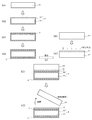
- a core 31 made of nitride ceramics is prepared (S01 in FIG. 2).
- a sealing layer 32 having a thickness of 0.05 ⁇ m or more and 1.5 ⁇ m or less is formed so as to wrap the core 31 to form a support substrate 3 (S02 in FIG. 2).
- the sealing layer 32 may be formed into a film by the LPCVD method.
- a flattening layer 4 having a thickness of 0.5 ⁇ m or more and 3.0 ⁇ m or less is formed on the upper surface of the support substrate 3 (S03 in FIG. 2).
- the flattening layer 4 may be formed by any of a plasma CVD method, an LPCVD method, and a low-pressure MOCVD method.
- a stress adjusting layer 5 is further formed on the lower surface of the support substrate 3 (S04 in FIG. 2). The flattening layer 4 and the stress adjusting layer 5 may be formed at the same time.
- a group III nitride single crystal substrate 20 for peeling and transferring the seed crystal layer 2 is prepared (S11 in FIG. 2).
- a specific method for preparing the single crystal substrate 20 will be described later.
- ion implantation is performed from one surface (ion implantation surface) of the single crystal substrate 20 to form a peeling position (embrittlement layer) 21 in the single crystal substrate 20 (S12 in FIG. 2). Ions implanted at this time, for example, H +, H 2 +, Ar +, or equal to He + and the like.
- the ion-implanted surface of the single crystal substrate 20 is bonded to the flattening layer 4 formed on the support substrate 3 to form a bonded substrate (S21 in FIG. 2).
- the single crystal substrate 20 is separated at the peeling position 21 of the single crystal substrate 20 in the bonded substrate (S22 in FIG. 2).
- a single crystal film of Si ⁇ 111>, SiC, sapphire, aluminum nitride, or aluminum gallium nitride is transferred as a seed crystal layer 2 on the flattening layer 4 on the support substrate 3.
- an uneven pattern is provided on the seed crystal layer 2.
- the support substrate 3, the flattening layer 4, and the seed crystal layer 2 provided with the uneven pattern are laminated to form a group III nitride-based composite substrate.
- the remaining portion of the separated group III nitride single crystal substrate 20 is used as a seed crystal for producing another group III nitride-based composite substrate by polishing the surface again to form an ion-implanted surface. It can be repeatedly used to transfer the layer to a thin film.
- the ion injection surface of the single crystal substrate 20 is once bonded to another temporary support substrate such as a silicon wafer, separated and the seed crystal layer 2 is bonded to the temporary support substrate, and the seed crystal layer 2 is bonded to the temporary support substrate.
- a step of separating the temporary support substrate from the seed crystal layer may be performed. By doing so, the seed crystal layer 2 bonded to the flattening layer 4 can be turned upside down.
- the single crystal substrate 20 a commercially available substrate can be used as it is for Si ⁇ 111>, SiC, or a sapphire substrate, which is easy to obtain as a commercially available substrate with a large diameter.
- a commercially available substrate can be used as it is for Si ⁇ 111>, SiC, or a sapphire substrate, which is easy to obtain as a commercially available substrate with a large diameter.
- aluminum nitride or aluminum gallium nitride which is difficult to obtain for a large-diameter substrate
- aluminum nitride or nitride is used on a large-diameter sapphire substrate by either the MOCVD method, the HVPE method, or the THVPE method (trihalide vapor phase growth method).
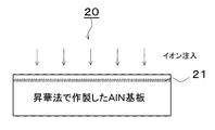
- FIG. 3 is a diagram showing a layer structure of a single crystal substrate 20 in the case of ion-implanting a plurality of small-diameter sublimation substrates into a laminated large-diameter substrate in the same direction.
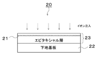
- the laminated substrate of the substrate is used as the base substrate 22, and an epitaxial film is formed on the substrate by any of the MOCVD method, the HVPE method, and the THVPE method, and the single crystal epitaxial layer substrate is used.
- the seed crystal layer 2 can be formed without consuming the expensive AlN substrate produced by the sublimation method, and the manufacturing cost can be reduced.
- the AlN substrate produced by the sublimation method is generally small in diameter, expensive and easy to color, but has excellent crystal characteristics. As shown in FIG. 3, a plurality of small-diameter single crystals are bonded together to prepare a large-diameter substrate, and then ion implantation is performed to perform thin film transfer to a thickness of 0.1 ⁇ m to 1.5 ⁇ m, and the remaining single crystal substrate remains. If the remainder of the above is reused for the production of the next composite substrate and used repeatedly, the cost for manufacturing the composite substrate can be reduced and the seed crystal functions as an extremely good seed crystal.
- the sublimation substrate is not used as a thick substrate of several hundred ⁇ m as in the past, but is used as an ultra-thin thin film of 0.1 ⁇ m to 1.5 ⁇ m in thin film transfer, so it is similar to the original substrate. Coloring does not matter.
- the thin film transfer is performed with a thickness of 0.1 ⁇ m to 1.5 ⁇ m, and the remaining portion of the remaining single crystal epitaxial layer substrate is reused for the production of the next composite substrate. You should use it.
- the single crystal epitaxial layer substrate can be used repeatedly, the cost for manufacturing the composite substrate can be significantly reduced.
- the epitaxial layer is epitaxially formed by any of the MOCVD method, the HVPE method, and the THVPE method, using the remaining portion of the single crystal epitaxial layer substrate whose epitaxial layer portion has become thin as the base substrate. By regenerating the layer, the first substrate can be used repeatedly, and the production cost can be further reduced.
- Example 1 (Preparation of support board) (1) AlN powder, the Y 2 O 3, 5 parts by weight to 100 parts by weight of the sintering aid, by mixing an organic binder, a solvent such as, after producing a green sheet, degreased, N 2 under, 1900 ° C. A double-sided polished ⁇ (diameter) 8 inch ⁇ t (thickness) 725 ⁇ m AlN substrate (AlN polycrystalline ceramic substrate) was used as a core.
- the damaged portion of the seed crystal layer damaged by the Si single crystal during ion implantation and transfer was lightly polished with CMP to make the thickness of the seed crystal layer 0.5 ⁇ m.
- a pattern of periodic irregularities having a groove depth of 0.3 ⁇ m, a groove width of 3 ⁇ m, and a terrace width of 5 ⁇ m was formed on the Si seed crystal layer.
- the rest of the Si single crystal substrate after thin film transfer (that is, the portion peeled off and separated without being transferred to the support substrate) can be used as a large number of seed crystals by repeatedly performing ion implantation, and is extremely. It was economical.
- ⁇ 8 having a support substrate having a structure of (1) an AlN ceramic core and (2) a sealing layer, a flattening layer having a thickness of 3 ⁇ m and a Si ⁇ 111> seed crystal layer having a thickness of 0.5 ⁇ m.
- An inch III nitride based epitaxial growth substrate was obtained.
- the above substrate was further evaluated as the following simple AlN epitaxial growth substrate. That is, 2 ⁇ m of AlN is formed on the AlN epitaxial substrate by the MOCVD method, and etch pits are generated by a molten alkali (KOH + NaOH) etching method in order to evaluate the dislocation density (Etch pit Density, hereinafter referred to as EPD).
- EPD Etch pit Density
- XRC X-ray locking curve
- the full width at half maximum FWHM in the XRC measurement of the (0002) plane of the substrate was 321 arcsec, and a high quality AlN single crystal was obtained. From these results, it can be seen that the epitaxial substrate according to this embodiment is excellent.
- the above substrate was further evaluated as the following simple AlN epitaxial growth substrate. That is, 2 ⁇ m of AlN was formed on the AlN epitaxial substrate by the MOCVD method, and etch pits were generated by the molten alkali (KOH + NaOH) etching method in order to evaluate the dislocation density, and EPD was measured.
- XRC measurement was performed as an evaluation of crystallinity. As a result, EPD showed an extremely low dislocation density of 3 ⁇ 10 6 cm- 2.
- the half-value width FWHM in the XRC measurement of the (0002) plane of the substrate was 731 arcsec, and both the dislocation density and the half-value width were inferior to those of Example 1.
- Example 2 (Preparation of support board)
- the core was an AlN polycrystalline ceramic substrate similar to that in Example 1.
- (2) First as the sealing layer covers the entire AlN ceramic core as encompassing at SiO 2 layer 0.5 ⁇ m thick by LPCVD method, in another LPCVD apparatus further thereon, a 0.8 ⁇ m thick Si 3 N The whole was sealed with four layers (total thickness of the sealing layer 1.3 ⁇ m) to prepare a support substrate.
- the AlN crystal used as a seed crystal was prepared by a sublimation method (improved release method) according to the following procedure.
- a TaC crucible was further placed in a growth container made of graphite that had been subjected to a high purification treatment, and a high-purity AlN raw material was provided at the bottom of the TaC crucible and AlN crystals were provided at the top.
- the growth vessel and crucible were heated by high-frequency induction heating, the raw material portion was kept at 2000 ° C., the raw material was sublimated and decomposed, and an AlN single crystal was precipitated on the upper AlN crystal.
- This AlN single crystal was sliced and polished to make a smooth ⁇ 2-inch substrate with a thickness of 200 ⁇ m.
- the resistivity was measured at 8 points in the plane of this substrate at equal intervals, it was 1 ⁇ 10 6 ⁇ ⁇ cm to 3 ⁇ 10 11 ⁇ ⁇ cm.
- the light transmittance at a wavelength of 230 nm was 0.2% in terms of thickness of 100 ⁇ m.
- the 2-inch substrate produced above was used as a regular hexagonal AlN substrate, and a plurality of the substrates were used, aligned with each other, and bonded to a ⁇ 8-inch quartz substrate. After that, the outer circumference of the quartz substrate was trimmed by cutting an excess portion so as to become a ⁇ 8 inch substrate. Ion implantation of hydrogen at a depth of 0.6 ⁇ m (peeling position) and a dose amount of 8 ⁇ 10 17 cm- 2 was carried out at 100 keV on the ⁇ 8 inch AlN single crystal substrate thus prepared. The ion-implanted surface of the AlN single crystal substrate after the ion implantation was bonded to the flattening layer of the support substrate prepared in advance.
- the seed crystal layer of the AlN single crystal was thin-film transferred to the support substrate by peeling and separating at the peeling position (0.6 ⁇ m portion).
- the damaged portion of the seed crystal layer damaged by the AlN single crystal during ion implantation and transfer was lightly polished with CMP to make the thickness of the AlN seed crystal layer 0.4 ⁇ m.
- a ⁇ 8 inch ⁇ 8 inch support substrate having a structure of (1) an AlN ceramic core and (2) a sealing layer is provided with a 2 ⁇ m-thick flattening layer and a 0.4 ⁇ m-thick AlN seed crystal layer.
- a group III nitride-based epitaxial growth substrate was obtained.
- the group III nitride-based epitaxial growth substrate obtained in this example was evaluated as a simple AlN epitaxial growth substrate in the same manner as in Example 1. That is, 2 ⁇ m of AlN was formed on the AlN epitaxial substrate by the MOCVD method, and EPD was measured by the molten alkali (KOH + NaOH) etching method in order to evaluate the dislocation density. In addition, XRC measurement was performed as an evaluation of crystallinity. As a result, EPD showed an extremely low dislocation density of 2.3 ⁇ 10 4 cm -2.
- the full width at half maximum FWHM in the XRC measurement of the (0002) plane of the substrate was 132 arcsec, and a high quality AlN single crystal was obtained. From these results, it can be seen that the epitaxial substrate according to this embodiment is excellent.
- Example 2 After transferring the AlN crystal to a thin film in Example 2, the conditions were the same except that the thin film was used as it was as a seed crystal layer without forming an off-angle at all.
- This epitaxial substrate was evaluated by forming a 2 ⁇ m AlN film by the MOCVD method in the same manner as in Example 2. As a result, the EPD was 6.5 ⁇ 10 6 cm- 2 . Further, the FWHM in the XRC measurement of the (0002) plane of the substrate was 1950 arcsec, and the quality of the crystal was considerably inferior to that of Example 2.
- Example 2 In order to increase the size of the seed substrate, a plurality of AlN substrates were used and bonded in the same direction, but it is considered that a slight difference in crystal orientation and the like adversely affected the crystal growth. On the contrary, in Example 2, it is considered that by positively providing the uneven pattern on the surface of the seed crystal layer, adverse effects on crystal growth such as these crystal defects and slight misalignment of orientation are absorbed. Will be.
- the substrate obtained from this comparative example had poor crystallinity and was unsuitable as an epitaxial substrate for growing a group III nitride single crystal for deep ultraviolet rays.
- Example 3 The conditions were the same except that the flattening layer was changed from SiO 2 having a thickness of 3 ⁇ m to Al As having a thickness of 2 ⁇ m in Example 1.
- a support substrate having a structure of (1) an AlN ceramic core and (2) a sealing layer was provided with a 2 ⁇ m-thick AlAs flattening layer and a 0.5 ⁇ m-thick Si ⁇ 111> seed crystal layer.
- a group III nitride-based epitaxial growth substrate was obtained.
- AlN was further laminated by the HVPE method on the group III nitride-based epitaxial growth substrate by 50 mm.
- This laminate was immersed in a 25% HCl aqueous solution to dissolve the AlAs layer, and 50 mm AlN crystals were separated from the support substrate.
- This AlN crystal was subjected to cylindrical grinding, slicing, and polishing to obtain 50 solid ⁇ 8 inch AlN single crystal substrates.
- Example 2 the same simple evaluation as in Example 1 was performed using the substrate as an AlN epitaxial substrate.
- EPD showed an extremely low dislocation density of 5.0 ⁇ 10 4 cm -2.
- the FWHM measured by XRC on the (0002) plane of the substrate was 132 arcsec, and a high quality AlN single crystal was obtained. No coloring was observed in this product, and the light transmittance at a wavelength of 230 nm was as good as about 90%, which was suitable as a device substrate in the deep ultraviolet region.
Landscapes
- Chemical & Material Sciences (AREA)
- Engineering & Computer Science (AREA)
- Organic Chemistry (AREA)
- Materials Engineering (AREA)
- Metallurgy (AREA)
- Crystallography & Structural Chemistry (AREA)
- Inorganic Chemistry (AREA)
- Chemical Kinetics & Catalysis (AREA)
- General Chemical & Material Sciences (AREA)
- Mechanical Engineering (AREA)
- Electromagnetism (AREA)
- Physics & Mathematics (AREA)
- Ceramic Engineering (AREA)
- Crystals, And After-Treatments Of Crystals (AREA)
- Recrystallisation Techniques (AREA)
- Structural Engineering (AREA)
- Manufacturing & Machinery (AREA)
Abstract
III族窒化物の単結晶を高品質で安価に作製可能なIII族窒化物エピタキシャル成長用基板とその製造方法を提供する。 本発明に係るIII族窒化物系エピタキシャル成長用基板は、窒化物セラミックスからなるコアが厚み0.05μm以上1.5μm以下の封止層で包み込まれた構造を有する支持基板と、支持基板の上面に設けられ、0.5μm以上3.0μm以下の厚みを有する平坦化層と、平坦化層の上面に設けられ、表面に凹凸パターンを有する0.1μm以上1.5μm以下の厚みの単結晶の種結晶層とを備える。
Description
本発明は、窒化アルミニウム(AlN)、窒化アルミニウムガリウム(AlxGa1-xN(ただし、0.<x<1.0)、窒化ガリウム(GaN)等のIII族窒化物単結晶のエピタキシャル成長に用いるための種基板に関する。
結晶性AlN系、GaN系等のIII族窒化物の基板は広いバンドギャップを有し、短波長の発光性や高耐圧で優れた高周波特性を持つ。このため、III族窒化物の基板は、発光ダイオード(LED)、レーザ、ショットキーダイオード、パワーデバイス、高周波デバイス等のデバイスへの応用に期待されている。特に AlNおよびAlxGa1-xN(0.5<x<1.0)の単結晶から作製されたLEDの深紫外線領域(UVC;200~280nm)の発光波長には殺菌効果が報告されており(非特許文献1)、更なる高品質化、大口径化、低価格化が求められている。
AlNは常圧下では融点を持たないことから、シリコン単結晶等で用いられる一般的な融液法での製造は難しい。
非特許文献2および非特許文献3には、1700~2250℃、N2雰囲気下で、SiCやAlNを種結晶として昇華法(改良レリー法)でAlN単結晶基板を製造する方法が記載されている。しかしながら、結晶成長に高温を要するなどの装置上の制約により、低コスト化が難しい上、φ4インチ以上の大口径化も困難であった。
また、特許文献1には、シリコン基板やAlN基板を下地基板としてハイドライド気相成長(HVPE)法でAlN層を成長させる方法が記載されている。しかしながら、この方法ではシリコンを下地基板に用いると熱膨張率や格子定数の違いに起因するAlN層の転位密度を低減することが困難である。一方、下地基板として結晶性の良い昇華法AlN基板を使うと転位密度を低減できる反面、下地基板自体が小口径でしかも高価なため、大口径基板での低コスト化が困難であった。これらの欠点を補うべく、非特許文献4にはベース基板と種基板を兼ねたサファイア基板上に一括、MOVPE法でAlN膜を5μm積層後、エッチングによりそこに溝を付けた後に、更にHVPE法で目的の厚みに成膜する方法が開示されている。上記の溝構造によりHVPE成膜時に形成されるボイドが熱膨張差による応力の緩和層として働き、その結果クラックが防止される。しかしこれはベース基板がφ4インチ以下の場合のみ有効であり、ベース基板がφ6、φ8、φ12インチ等の大口径の場合はクラックや大きな反りが発生し問題であった。
特許文献2には、熱膨張率がAlN単結晶に近く低廉なAlNセラミックスをベース基板とし、このベース基板をSi3N4等で封止した上でシリコン<111>単結晶を薄膜転写した複合基板を種結晶としてGaN単結晶などのIII族窒化物をエピタキシャル成長させる方法が記載されている。しかしながら、この方法で例えばAlNやAlxGa1-xN(0<x<1)の単結晶をエピタキシャル成膜すると、シリコン<111>の種結晶と目的のAlNやAlxGa1-xN(0<x<1)の単結晶の格子定数の違いから転位密度を低減することが難しく、また封止層や平坦化層等との親和性や熱膨張率差などで成膜基板のクラックや反りを小さくするのも難しい。これらは、後工程のデバイス製作における特性劣化や歩留まり低下に影響し、結果的に作製されるレーザやLED、高周波デバイス等の高品質化、低コスト化の妨げとなっていた。
そこで、本発明者等はこれ等の欠点を排除すべく、鋭意検討した結果、本発明に至ったものである。
LEDs Magazine Japan;2016年12月、p30~p31
SEIテクニカルレビュー;No.177号、p88~p91
フジクラ技報;No.119号、2010年Vol.2、p33~p38
Journal of Crystal Growth 411(2015)、p38~p44
本発明は上記事情に鑑みなされたものであり、III族窒化物、特に深紫外線領域(UVC;200~280nm)の発光ダイオード用として好適なAlNやAlxGa1-xN(0.5<x<1.0)の単結晶を大口径で高品質、安価に作製可能なIII族窒化物エピタキシャル成長用基板とその製法を提供することを目的とする。
本発明は発明者等の多くの試行の結果により、
(1)窒化物セラミックスからなるコアが厚み0.05μm以上1.5μm以下の封止層で包み込まれた構造を有する支持基板と、
前記支持基板の上面に設けられ、0.5μm以上3.0μm以下の厚みを有する平坦化層と、
前記平坦化層の上面に設けられ、表面に凹凸パターンを有する0.1μm以上1.5μm以下の厚みの単結晶の種結晶層と
を備えること、
(2)支持基板(ベース基板)とエピ膜とが略同じ熱膨張率を有すること、
(3)凹凸パターンが薄膜転写した種結晶表面に周期的な溝やドット構造、あるいは0.1~3°のオフ・アングルのパターン形成をすること、
により、大口径でもクラックや反りを発生させず、又、成膜時の結晶欠陥を側面に集中させ、高純度、高品質のエピ結晶成長ができるIII族窒化物系エピタキシャル成長用基板と、その製造方法を発明したものである。本発明は上記の(1)、(2)、(3)の個々の要素により効果を得るものであるが、3者が揃った場合に相乗効果により極めて顕著な効果が得られるものである。
(1)窒化物セラミックスからなるコアが厚み0.05μm以上1.5μm以下の封止層で包み込まれた構造を有する支持基板と、
前記支持基板の上面に設けられ、0.5μm以上3.0μm以下の厚みを有する平坦化層と、
前記平坦化層の上面に設けられ、表面に凹凸パターンを有する0.1μm以上1.5μm以下の厚みの単結晶の種結晶層と
を備えること、
(2)支持基板(ベース基板)とエピ膜とが略同じ熱膨張率を有すること、
(3)凹凸パターンが薄膜転写した種結晶表面に周期的な溝やドット構造、あるいは0.1~3°のオフ・アングルのパターン形成をすること、
により、大口径でもクラックや反りを発生させず、又、成膜時の結晶欠陥を側面に集中させ、高純度、高品質のエピ結晶成長ができるIII族窒化物系エピタキシャル成長用基板と、その製造方法を発明したものである。本発明は上記の(1)、(2)、(3)の個々の要素により効果を得るものであるが、3者が揃った場合に相乗効果により極めて顕著な効果が得られるものである。
上記の課題を解決すべく本発明の実施形態に係るIII族窒化物系エピタキシャル成長用基板は、窒化物セラミックスからなるコアが厚み0.05μm以上1.5μm以下の封止層で包み込まれた構造を有する支持基板と、支持基板の上面に設けられ、0.5μm以上3.0μm以下の厚みを有する平坦化層と、平坦化層の上面に設けられ、表面に凹凸パターンを有する0.1μm以上1.5μm以下の厚みの単結晶の種結晶層とを備える。
本発明では、III族窒化物系エピタキシャル成長用基板は、支持基板の下面に応力調整層を更に備えるとよい。
本発明では、コアは、窒化アルミニウムセラミックスであるとよい。また、封止層は、窒化ケイ素を含むとよい。また、平坦化層は、酸化ケイ素、酸窒化ケイ素、及びヒ化アルミニウムのいずれかを含むとよい。また、応力調整層が、単体のシリコンを含むとよい。
本発明では、種結晶層は、Si<111>、SiC、サファイア、窒化アルミニウムまたは窒化アルミニウムガリウムであるとよい。そして、種結晶層の凹凸パターンが、周期的な溝、0.1~3°のオフ・アングル、およびドット構造から選ばれることが好ましい。また、種結晶層が窒化アルミニウムまたは窒化アルミニウムガリウムの場合には抵抗率が1×10⁶Ω・cm以上であることが好ましい。
また、本発明の実施形態に係るIII族窒化物系エピタキシャル成長用基板の製造方法は、窒化物セラミックスからなるコアを用意するステップと、コアを包み込むように厚み0.05μm以上1.5μm以下の封止層を成膜して支持基板とするステップと、支持基板の上面に厚み0.5μm以上3.0μm以下の平坦化層を成膜するステップと、平坦化層の上面に、表面が凹凸パターンを有する0.1μm以上1.5μm以下の厚みの単結晶の種結晶層とを設けるステップとを備える。
III族窒化物系エピタキシャル成長用基板の製造方法は、支持基板の下面に応力調整層を成膜するステップを更に備えるとよい。
本発明では、封止層をLPCVD法で成膜するとよい。また、平坦化層をプラズマCVD法、LPCVD法、および低圧MOCVD法のいずれかで成膜するとよい。
本発明では、種結晶層を設けるステップは、1面をイオン注入面とするIII族窒化物の単結晶基板を用意するステップと、イオン注入面からイオン注入して単結晶基板に剥離位置を形成するステップと、イオン注入面と平坦化層とを接合して接合基板するステップと、接合基板を剥離位置で種結晶層と単結晶基板残部とに分離するステップと前記で得られた種結晶層に凹凸パターンを設けるステップとを備えるとよい。
本発明では、単結晶基板を用意するステップにおいて、大口径の基板を市販基板として得易いSi<111>、SiC、或いはサファイア基板については、市販基板をそのまま利用することができる。一方、大口径が得難い窒化アルミニウムまたは窒化アルミニウムガリウムの場合は、大口径のサファイア基板上でMOCVD、HVPE法、およびTHVPE法のいずれかにより、窒化アルミニウムまたは窒化アルミニウムガリウムを積層して単結晶の大口径基板を作製して用いるとよい。あるいは、昇華法で作製した小口径の単結晶若しくは昇華法で作製したAlN基板を下地としてHVPE法、HVPE法、およびTHVPE法のいずれかで窒化アルミニウムまたは窒化アルミニウムガリウムのエピタキシャル層をエピタキシャル成長して得られる小口径の単結晶を貼り合わせて単結晶基板を得るとよい。
また、単結晶基板にエピタキシャル層が積層されている場合には、剥離位置を形成するステップにおいて、剥離位置をエピタキシャル層内に形成するとよい。この場合、単結晶基板残部を、下地基板として再利用するとよい。あるいは、単結晶基板残部を、更に別のIII族窒化物系複合基板の製造における単結晶基板として再利用するとよい。
本発明では、コアは、窒化アルミニウムセラミックスであるとよい。また、封止層は、窒化ケイ素を含むとよい。また、平坦化層は、酸化ケイ素、酸窒化ケイ素、及びヒ化アルミニウムのいずれかを含むとよい。また、応力調整層が、単体のシリコンを含むとよい。
本発明では、種結晶層は、種結晶層が、Si<111>、SiC、窒化アルミニウムまたは窒化アルミニウムガリウムであるとよい。そして、種結晶層には凹凸パターンが形成されるとよい。凹凸パターンは、周期的な溝、0.1~3°のオフ・アングル、およびドット構造から選ばれることが好ましい。また、種結晶層の抵抗率は、1×10⁶Ω・cm以上であることが好ましい。
本発明によれば、高品質で大口径なIII族窒化物の単結晶を安価に作製可能なIII族窒化物エピタキシャル成長用基板を提供することができる。
以下、本発明の実施形態について詳細に説明するが、本発明は、これらに限定されるものではない。
本実施形態に係る複合基板1の断面構造を図1に示す。図1に示した複合基板1は、支持基板3上に平坦化層4及び表面が凹凸パターンを有する0.1μm以上1.5μm以下の厚みの単結晶の種結晶層2が積層された構造を備えている。また、必要に応じて、支持基板3の平坦化層4が積層された面とは反対の面(下面)には、応力調整層5が設けられる。
支持基板(ベース基板)3は、当該支持基板3の芯材となるコア31と、コア31を覆う封止層32とを備える。
コア31に用いる材料は、耐熱性や安定性に優れ、大口径サイズを安価に入手できる窒化物セラミックスが好ましい。窒化物セラミックスとしては、窒化アルミニウム(AlN)、窒化ケイ素(Si3N4)、窒化ガリウム(GaN)、窒化ホウ素(BN)またはこれらの混合体などを用いることができる。AlNは、目的のIII族窒化物結晶と格子定数や熱膨張係数が近いので変形の少ない高品質のIII族窒化物結晶を作製することが可能であり、特に好ましい。また、AlNは、熱伝導性が高いため、加熱を含む後工程における熱伝達に優れる点でも好ましい。
コア31の形状およびサイズは、厚さ200~1000μmのウエハー形状とすると、通常の半導体プロセスラインにのせることができるので好ましい。加えて、コア31の表面を鏡面仕上げとしておくと、支持基板3の表面の凹凸を低減でき好ましい。
AlNをコア31として用いる場合、AlNセラミックスの製造方法は種々あるが、AlN粉と焼結助剤、有機バインダー、溶剤などを混合して、ウエハー状のグリーンシートを作製、脱脂した後にN2雰囲気下で焼結して研磨する、所謂シート成型/常圧焼結法を用いることが生産性を高くできる点で好ましい。焼結助剤としては、Y2O3、Al2O3、CaO等から選ばれるが、特にY2O3を焼結助剤として含むと焼結後の基板の熱伝導性が高く発現するため好適である。
封止層32は、コア全体を覆うように隙間無く包み込んで封止する層であり、0.05μm以上1.5μm以下の厚みを有する。このような構造とすることで、コア31のセラミックス材料に起因する物質が支持基板3の外部に漏出するのを防ぐことができる。
例えばAlNセラミックスをコア31として用いるとAlNや焼結助剤として加えたY2O3に起因する元素物質や、セラミックスを焼結する際に用いた断熱材や炉材、容器などから不純物としてセラミックスに取り込まれた物質が漏出する可能性がある。このような物質が支持基板3の外に漏出すると、目的とするAlNをエピタキシャル成長させる際に不純物として取り込まれて、品質を低下させる要因となりやすい。
封止層32の厚みが厚いと後工程で加熱冷却を繰り返した際に封止層32の表層と内部との間の熱応力に耐えられなくなり、剥離が生じやすい。したがって種々の膜を選び、組み合わせたとしても封止層32は1.5μmを超える厚みは好ましくない。一方、コア31に起因する物質を封止する機能としては厚みが0.05μm未満では不十分である。以上のことから、封止層32の厚みは0.05μm以上1.5μm以下の範囲が好ましい。窒化物セラミックスに起因する材料物質を封止する効果が高いため、封止層32の材料は窒化ケイ素(Si3N4)よりなる膜が好ましい。
封止層32は、緻密な膜となっていると、封止性能が高まるので好ましい。また、封止層32は、焼結助剤などの不純物を含まず、純度が高い膜になっていること好ましい。このようにすることで封止層32は、自体に起因する意図せぬ物質の支持基板3の外への漏出が抑制されるので好ましい。
このような、高純度な膜はMOCVD法、常圧CVD法、LPCVD(低圧CVD)法、スパッター法、などの成膜法を用いて成膜することができる。特にLPCVD法を用いると緻密な膜を形成できるうえ、膜のカバレッジ性に優れるため好ましい。
また、封止層32の材料として窒化ケイ素を用いる際、窒化ケイ素とコアとの密着性を高めるために、酸化ケイ素(SiO2)や酸窒化ケイ素(SixOyNz)などの膜を封止層の一部としてコア31との間に設けてもよい。しかしその場合でも剥離を避けるため、封止層32全体の厚みは0.05μm以上1.5μm以下の範囲とすることが好ましい。
支持基板3の上面には、封止層32上に厚み0.5μm以上3.0μm以下の平坦化層3が積層される。平坦化層4を積層することにより、コア31や封止層32などに起因する種々のボイドや凹凸を埋め、種結晶が転写するために十分な平滑性が得られる。ただし、平坦化層4の厚みが厚過ぎると反り等の原因になり、好ましくない。このため、平坦化層4の厚みは0.5~3.0μmが好適である。即ち、平坦化層4の厚みが0.5μm未満だと支持基板3に生じたボイドや凹凸を十分に埋めることができないため好ましくない。また、平坦化層4の厚みが3.0μm以上だと反りが発生し易いため好ましくない。
なお、支持基板3の平坦化層4が積層された上面とは反対側の面(下面)には、応力調整層5を設けられる。応力調整層5は、平坦化層4を積層することにより生じる応力を相殺し、反りを低減する。
また、平坦化層4は支持基板3の種結晶層2を積層する側の片面(上面)のみに積層すればよいが、支持基板の両面(上面および下面)若しくは支持基板全体を覆うように成膜してもよい。このようにすると下面に積層した材料が応力調整層5として作用し、基板上下で平坦化層4に起因する応力が構造上相殺されるので基板の反りが更に低減される。
また、応力調整層5として、単体のシリコン(多結晶シリコンなど)を積層してもよい。このようにすることで、静電チャックによる吸着・離脱にも対応した複合基板となる利点がある。
平坦化層4の材料は、酸化ケイ素(SiO2)、酸化アルミニウム(Al2O3)、窒化ケイ素(Si3N4)、炭化ケイ素(SiC)或いは酸窒化ケイ素(SixOyNz)や、シリコン(Si)、ヒ化ガリウム(GaAs)、ヒ化アルミニウム(AlAs)等から選ぶとよい。特に、酸化ケイ素(SiO2)、酸窒化ケイ素(SixOyNz)、ヒ化アルミニウム(AlAs)は、平坦化時の研削や研磨が容易で且つ、目的とするAlN等のIII族窒化物をエピタキシャル成長した後、支持基板3を分離するための犠牲層になり易いので好ましい。
平坦化層4の成膜はプラズマCVD法又はLPCVD法、或いは低圧MOCVD法などからその必要膜質と成膜効率から任意に選ぶことができる。積層された平坦化層4の膜の状況により、成膜後に焼き締めの熱処理やCMP研磨を施し、種結晶層2の形成に備えられる。
支持基板3の上面に形成された平坦化層4の上には高品質なSi<111>、SiC、サファイア、窒化アルミニウムまたは窒化アルミニウムガリウムの単結晶からなる種結晶層2が形成される。種結晶層2は、表面に凹凸パターンを有する。種結晶層2の厚みは0.1μm以上1.5μm以下とすることが好ましい。このようにすることで、高品質な種結晶層2を形成することが可能になる。即ち、上記の単結晶の基板に対してイオン注入剥離を適用して高品質な結晶層を薄膜転写することができる。種結晶層2の厚みが0.1μm未満ではイオン注入時のダメージ層が略、その厚みに近いため、良好な種結晶とは成り得ない。また、種結晶層2の厚みが1.5μm以上になるとイオン注入装置が莫大な大きさになり、莫大な投資を必要とし、現実的でない。
このとき使用される高品質の上記の単結晶とは、一般の溶融法(CZ法、FZ法)、昇華法、MOCVD法(有機金属気相成長法)、HVPE(ハイドライド気相成長法)法、およびTHVPE法(トリハライド気相成長法)の何れかによって、得られる単結晶、あるいはエピタキシャル成長した単結晶であることが好ましい。また当該単結晶のEPDは1×106cm-2以下と極めて低い転位密度の結晶であることが好ましい。
また、種結晶層2の表面の凹凸パターンは、Si<111>、SiC、サファイア、窒化アルミニウムまたは窒化アルミニウムガリウムをイオン注入剥離により薄膜転写した後に、その表面にリソグラフィーで数μ~数十μmの周期的な溝やドット構造を作製するか、あるいはエッチング等により0.1~3度のオフ・アングルを形成することにより形成することができる。パターンはその種結晶基板の性状により、適宜、選ばれる。
種結晶層2は、目的とするエピタキシャル成長させる膜の組成と一致する必要はないが結晶型が類似し、できるだけその格子定数もAlNに近いことが好ましい。一方、熱膨張率はAlNに近いに越したことはないが、種結晶層2は薄膜転写により極薄く形成されるため、コアのベース基板に比べ、反りへの影響はほとんど無視することができる。これに対して、ベース基板と種結晶を兼ねた厚い種結晶基板においては、エピタキシャル成長させる膜との熱膨張率に差がある場合、成膜時の基板の反りが大きく、割れやクラックが発生する。
また、種結晶層2が窒化アルミニウムまたは窒化アルミニウムガリウムの場合は、その抵抗率が1×10⁶Ω・cm以上とすることが好ましい。このようにすると、種結晶層2上にエピタキシャル成膜された目的材料に取り込まれる不純物を低減でき、目的材料の着色(すなわち光吸収)を抑制することができる。
続いて、図2を参照して、本実施形態に係るIII族窒化物系エピタキシャル成長用基板の製造方法の手順を説明する。はじめに、窒化物セラミックスからなるコア31を準備する(図2のS01)。続いて、コア31を包み込むように厚み0.05μm以上1.5μm以下の封止層32を成膜して支持基板3とする(図2のS02)。このとき、封止層32は、LPCVD法で成膜するとよい。
続いて、支持基板3の上面に厚み0.5μm以上3.0μm以下の平坦化層4を成膜する(図2のS03)。平坦化層4は、プラズマCVD法、LPCVD法、および低圧MOCVD法のいずれかで成膜するとよい。また、支持基板3の下面に応力調整層5を更に成膜する(図2のS04)。なお、平坦化層4と応力調整層5は同時に製膜してもよい。
また、S01~S04とは別に、種結晶層2を剥離転写するためのIII族窒化物の単結晶基板20を用意する(図2のS11)。この単結晶基板20を用意する具体的な手法については後述する。続いて、単結晶基板20の1面(イオン注入面)からイオン注入を行い、単結晶基板20内に剥離位置(脆化層)21を形成する(図2のS12)。このとき注入するイオンは、例えば、H+、H2
+、Ar+、He+等とするとよい。
次に、単結晶基板20のイオン注入面を、支持基板3上に形成した平坦化層4と接合して接合基板とする(図2のS21)。そして、接合基板における単結晶基板20の剥離位置21で、単結晶基板20を分離する(図2のS22)。このようにすることによって、支持基板3の上の平坦化層4の上にSi<111>、SiC、サファイア、窒化アルミニウムまたは窒化アルミニウムガリウムのいずれかの単結晶膜が種結晶層2として薄膜転写され、剥離位置21で種結晶層2と単結晶基板20の残部とに分離した後、種結晶層2に凹凸パターンを設ける。これらの工程を経て支持基板3、平坦化層4、凹凸パターンが設けられた種結晶層2が積層され、III族窒化物系複合基板となる。一方、分離されたIII族窒化物の単結晶基板20の残部は、再びこの表面を研磨してイオン注入面とすることによって、更に別のIII族窒化物系複合基板を作製する際の種結晶層を薄膜転写するために繰り返し利用することができる。
なお、単結晶基板20のイオン注入面を一旦シリコンウエハ等の別の仮支持基板に接合して、分離して種結晶層2が仮支持基板に接合した状態にしておき、この仮支持基板上の種結晶層2を平坦化層4に接合した上で、仮支持基板を種結晶層から切り離す工程を行ってもよい。このようにすることで、平坦化層4に接合する種結晶層2の上下を反転することができる。
続いて、単結晶基板20を用意する方法について説明する。単結晶基板20は大口径基板が市販基板として得易いSi<111>、SiC、あるいはサファイア基板については、そのまま、市販基板を利用することができる。一方、大口径の基板が得難い窒化アルミニウムまたは窒化アルミニウムガリウムの場合は、大口径のサファイア基板上でMOCVD法、HVPE法、およびTHVPE法(トリハライド気相成長法)のいずれかにより、窒化アルミニウムまたは窒化アルミニウムガリウムを積層して単結晶の大口径基板を作製して用いるとよい。あるいは昇華法で作製した小口径の基板(昇華法基板)を使う場合、若しくは昇華法で作製したAlN基板を下地としその上にMOCVD法、HVPE法、THVPE法のいずれかで窒化アルミニウムまたは窒化アルミニウムガリウムを積層した結晶を使う場合には、小口径の単結晶を貼り合わせて大口径基板を作製して用いるとよい。
図3は小口径の昇華法基板を、方位を合せて複数枚、貼り合せた大口径基板にイオン注入する場合の単結晶基板20の層構造を示す図である。図4は上記基板の貼り合せ基板を下地基板22とし、更にその上にMOCVD法、HVPE法、THVPE法のいずれかの方法でエピタキシャル成膜を行い、この単結晶エピタキシャル層基板を用いる場合の単結晶基板20の層構造を示す図である。この場合、イオン注入による剥離位置21をエピタキシャル層23内に設定するとよい。このようにすれば、昇華法で作製した高価なAlN基板を消費することなく種結晶層2を形成することが可能となり、製造コストを低減できる。加えて、MOCVD法、HVPE法、およびTHVPE法のいずれかの方法でAlxGa1-xN単結晶をエピタキシャル成膜形成する場合は、原料ガス組成などを調整することによってAlxGa1-xNのxの値を0≦x≦1の間を変化させることができるので、目的とする後工程のエピタキシャル成長に最適な値を選択できる利点がある。
なお、昇華法で作製したAlN基板は一般に小口径、高価で着色し易いが、結晶特性が優れている。図3のように、小口径の単結晶を複数枚、貼り合せて大口径基板を作製した後、イオン注入して0.1μm~1.5μmの厚みで薄膜転写を行い、残った単結晶基板の残部を次の複合基板の作製に再利用することにより繰り返し使用すれば、複合基板の作製にかかるコストも低減できる上、極めて良好な種結晶として機能する。加えて、これまでのように昇華法の基板を数百μmの厚い基板として使用せず、薄膜転写で、0.1μm~1.5μmの極薄い薄膜状で使うため、元の基板のような着色は問題にならない。
更に、図4のように剥離位置をエピタキシャル層内に設定した場合、0.1μm~1.5μmの厚みで薄膜転写を行い残った単結晶エピタキシャル層基板の残部を次の複合基板の作製に再利用するとよい。このようにすれば単結晶エピタキシャル層基板を繰り返し使用できるので、複合基板の作製にかかるコストを著しく低減できる。また、繰り返し使用の結果、エピタキシャル層部分が薄くなった単結晶エピタキシャル層基板の残部を下地基板として、エピタキシャル層をMOCVD法、HVPE法、THVPE法のいずれかの方法でエピタキシャル成膜をすることによりエピタキシャル層を再生すれば、最初の下地基板を繰り返し使用することができ、作製コストを更に低減することができる。
以下に実施例及び比較例を挙げて、本発明をさらに具体的に説明するが、本発明はこれら実施例に限定されるものではない。
[実施例1]
(支持基板の準備)
(1)AlN粉、100重量部と焼結助剤としてY2O3、5重量部を、有機バインダー、溶剤などと混合して、グリーンシートを作製後、脱脂し、N2下、1900℃で焼結した、両面研磨のφ(直径)8インチ×t(厚み)725μmのAlN基板(AlN多結晶セラミックス基板)をコアとした。(2)このコア全体をLPCVD法により0.2μm厚の酸窒化珪素層で包み込むように覆い、その上に更に別LPCVD装置を使い、0.6μm厚の窒化ケイ素(Si3N4)層で全体を包み込むように覆って、封止(封止層の総厚み=0.8μm)し、支持基板とした。
(支持基板の準備)
(1)AlN粉、100重量部と焼結助剤としてY2O3、5重量部を、有機バインダー、溶剤などと混合して、グリーンシートを作製後、脱脂し、N2下、1900℃で焼結した、両面研磨のφ(直径)8インチ×t(厚み)725μmのAlN基板(AlN多結晶セラミックス基板)をコアとした。(2)このコア全体をLPCVD法により0.2μm厚の酸窒化珪素層で包み込むように覆い、その上に更に別LPCVD装置を使い、0.6μm厚の窒化ケイ素(Si3N4)層で全体を包み込むように覆って、封止(封止層の総厚み=0.8μm)し、支持基板とした。
(平坦化層の積層)
支持基板の片面(上面)のSi3N4層上に更に平坦化の目的で、プラズマCVD法(ICP―CVD装置)で7μm厚のSiO2を積層した。その後、このSiO2を1000℃で焼き締めた後、CMP研磨により、3μm厚まで研磨・平坦化し表面粗さRa=0.15nmとした。
支持基板の片面(上面)のSi3N4層上に更に平坦化の目的で、プラズマCVD法(ICP―CVD装置)で7μm厚のSiO2を積層した。その後、このSiO2を1000℃で焼き締めた後、CMP研磨により、3μm厚まで研磨・平坦化し表面粗さRa=0.15nmとした。
(種結晶の準備)
市販のCZ法で引き上げたφ8インチSi<111>基板に100keVで水素を深さ0.7μm(剥離位置)、ドース量6×1017cm-2のイオン注入を実施した。このイオン注入後のAlN単結晶基板のイオン注入面と、先に準備しておいた支持基板の平坦化層とを接合した。その後、剥離位置(0.7μm部分)で剥離・分離することによってAlN単結晶の種結晶層を支持基板に薄膜転写した。イオン注入と転写の際に種結晶層のSi単結晶が受けたダメージ部分をCMPで軽く研磨し、Si種結晶層の厚みを0.5μmとした。このSi種結晶層に溝深さ0.3μm、溝幅3μm、テラス幅5μmの周期的な凹凸のパターンを形成した。薄膜転写後のSi単結晶基板の残部(すなわち、支持基板に転写されずに剥離・分離された部分)は、イオン注入を何度も繰り返し実施することにより、多数の種結晶として利用でき、極めて経済的であった。以上により(1)AlNのセラミック・コアと(2)封止層との構造を有する支持基板に、3μm厚の平坦化層及び、0.5μm厚のSi<111>種結晶層を備えたφ8インチのIII族窒化物系エピタキシャル成長用基板が得られた。
市販のCZ法で引き上げたφ8インチSi<111>基板に100keVで水素を深さ0.7μm(剥離位置)、ドース量6×1017cm-2のイオン注入を実施した。このイオン注入後のAlN単結晶基板のイオン注入面と、先に準備しておいた支持基板の平坦化層とを接合した。その後、剥離位置(0.7μm部分)で剥離・分離することによってAlN単結晶の種結晶層を支持基板に薄膜転写した。イオン注入と転写の際に種結晶層のSi単結晶が受けたダメージ部分をCMPで軽く研磨し、Si種結晶層の厚みを0.5μmとした。このSi種結晶層に溝深さ0.3μm、溝幅3μm、テラス幅5μmの周期的な凹凸のパターンを形成した。薄膜転写後のSi単結晶基板の残部(すなわち、支持基板に転写されずに剥離・分離された部分)は、イオン注入を何度も繰り返し実施することにより、多数の種結晶として利用でき、極めて経済的であった。以上により(1)AlNのセラミック・コアと(2)封止層との構造を有する支持基板に、3μm厚の平坦化層及び、0.5μm厚のSi<111>種結晶層を備えたφ8インチのIII族窒化物系エピタキシャル成長用基板が得られた。
(基板の評価)
次いで、更に上記基板に対し以下の簡便なAlNエピタキシャル成長用基板としての評価を行った。即ち、上記AlNエピタキシャル用基板にMOCVD法で2μmのAlNを成膜し、転位密度を評価するべく溶融アルカリ(KOH+NaOH)エッチング法によりエッチピットを発生させエッチピット密度(Etch pit Density、以下EPDという)の測定を行った。また、結晶性の評価としてX線ロッキングカーブ(XRC)測定を行った。その結果、EPDは3×105cm-2と極めて低い転位密度を示した。また、基板の(0002)面のXRC測定での半値幅FWHMは321arcsecとなり、高品質のAlN単結晶が得られた。これらの結果から、本実施例によるエピタキシャル用基板は優れていることが分かる。
次いで、更に上記基板に対し以下の簡便なAlNエピタキシャル成長用基板としての評価を行った。即ち、上記AlNエピタキシャル用基板にMOCVD法で2μmのAlNを成膜し、転位密度を評価するべく溶融アルカリ(KOH+NaOH)エッチング法によりエッチピットを発生させエッチピット密度(Etch pit Density、以下EPDという)の測定を行った。また、結晶性の評価としてX線ロッキングカーブ(XRC)測定を行った。その結果、EPDは3×105cm-2と極めて低い転位密度を示した。また、基板の(0002)面のXRC測定での半値幅FWHMは321arcsecとなり、高品質のAlN単結晶が得られた。これらの結果から、本実施例によるエピタキシャル用基板は優れていることが分かる。
[比較例1]
実施例1でSi種結晶層に凹凸のパターンを形成せず、フラットなSi<111>とした以外は全て同じ条件とした。本実施により(1)AlNのセラミック・コアと(2)封止層との構造を有する支持基板に、3μm厚の平坦化層及び、0.5m厚のSi<111>種結晶層を備えたφ8インチのIII族窒化物系エピタキシャル成長用基板が得られた。
実施例1でSi種結晶層に凹凸のパターンを形成せず、フラットなSi<111>とした以外は全て同じ条件とした。本実施により(1)AlNのセラミック・コアと(2)封止層との構造を有する支持基板に、3μm厚の平坦化層及び、0.5m厚のSi<111>種結晶層を備えたφ8インチのIII族窒化物系エピタキシャル成長用基板が得られた。
(基板の評価)
次いで、更に上記基板に対し以下の簡便なAlNエピタキシャル成長用基板としての評価を行った。即ち、上記AlNエピタキシャル用基板にMOCVD法で2μmのAlNを成膜し、転位密度を評価するために溶融アルカリ(KOH+NaOH)エッチング法によりエッチピットを発生させEPDの測定を行った。また、結晶性の評価としてXRC測定を行った。その結果、EPDは3×106cm-2と極めて低い転位密度を示した。また、基板の(0002)面のXRC測定での半値幅FWHMは731arcsecとなり、転位密度、半値幅ともに実施例1より劣る結晶であった。
次いで、更に上記基板に対し以下の簡便なAlNエピタキシャル成長用基板としての評価を行った。即ち、上記AlNエピタキシャル用基板にMOCVD法で2μmのAlNを成膜し、転位密度を評価するために溶融アルカリ(KOH+NaOH)エッチング法によりエッチピットを発生させEPDの測定を行った。また、結晶性の評価としてXRC測定を行った。その結果、EPDは3×106cm-2と極めて低い転位密度を示した。また、基板の(0002)面のXRC測定での半値幅FWHMは731arcsecとなり、転位密度、半値幅ともに実施例1より劣る結晶であった。
[実施例2]
(支持基板の準備)
支持基板の構造として(1)コアは実施例1と同様のAlN多結晶セラミックス基板とした。(2)この封止層としてまず、AlNセラミックス・コア全体をLPCVD法による0.5μm厚のSiO2層で包み込む様に覆い、その上に更に別LPCVD装置で、0.8μm厚のSi3N4層で全体を封止(封止層の総厚み=1.3μm)し、支持基板とした。
(支持基板の準備)
支持基板の構造として(1)コアは実施例1と同様のAlN多結晶セラミックス基板とした。(2)この封止層としてまず、AlNセラミックス・コア全体をLPCVD法による0.5μm厚のSiO2層で包み込む様に覆い、その上に更に別LPCVD装置で、0.8μm厚のSi3N4層で全体を封止(封止層の総厚み=1.3μm)し、支持基板とした。
(平坦化層ならびに応力調整層の積層)
支持基板の片面(上面)のSi3N4層上に更に平坦化の目的で、LPCVD法により酸窒化珪素を4μm積層した。その後、CMP研磨で酸窒化珪素層を3μm厚とした。基板全体が約30μmと大きく反ったため、その反りを矯正すべく、下面に応力調整層として、酸窒化珪素をLPCVD法により5μm厚で積層した。その後、静電チャックによる吸着・脱着に対応すべく、更にLPCVD法で多結晶Siを0.2μm付け加えた。その結果、反りが略、解消し静電チャックへの吸着・脱着も可能となった。
支持基板の片面(上面)のSi3N4層上に更に平坦化の目的で、LPCVD法により酸窒化珪素を4μm積層した。その後、CMP研磨で酸窒化珪素層を3μm厚とした。基板全体が約30μmと大きく反ったため、その反りを矯正すべく、下面に応力調整層として、酸窒化珪素をLPCVD法により5μm厚で積層した。その後、静電チャックによる吸着・脱着に対応すべく、更にLPCVD法で多結晶Siを0.2μm付け加えた。その結果、反りが略、解消し静電チャックへの吸着・脱着も可能となった。
(種結晶の準備)
種結晶として用いるAlN結晶は、以下の手順による昇華法(改良レリー法)で作製した。まず、高純度化処理をした黒鉛製の成長容器中に更にTaC製坩堝を入れ、そのTaC坩堝の底部に高純度AlN原料を、上部にAlN結晶を設けた。高周波誘導加熱により成長容器と坩堝を加熱し、原料部を2000℃に保ち、原料の昇華分解を行い、上部のAlN結晶上にAlN単結晶を析出させた。このAlN単結晶をスライスし、研磨して厚さ200μmの平滑なφ2インチ基板を作った。因みに、この基板の面内8点等間隔で抵抗率を測定したところ、1×10⁶Ω・cm~3×10¹¹Ω・cmであった。また、波長230nmの光透過率は厚み100μm換算で0.2%であった。
種結晶として用いるAlN結晶は、以下の手順による昇華法(改良レリー法)で作製した。まず、高純度化処理をした黒鉛製の成長容器中に更にTaC製坩堝を入れ、そのTaC坩堝の底部に高純度AlN原料を、上部にAlN結晶を設けた。高周波誘導加熱により成長容器と坩堝を加熱し、原料部を2000℃に保ち、原料の昇華分解を行い、上部のAlN結晶上にAlN単結晶を析出させた。このAlN単結晶をスライスし、研磨して厚さ200μmの平滑なφ2インチ基板を作った。因みに、この基板の面内8点等間隔で抵抗率を測定したところ、1×10⁶Ω・cm~3×10¹¹Ω・cmであった。また、波長230nmの光透過率は厚み100μm換算で0.2%であった。
上記で作製の2インチ基板を正六角形のAlN基板とし、その複数枚を使い、方位を合せてφ8インチの石英基板に接着し、貼り合せた。その後、石英基板の外周をφ8インチ基板になる様に余分な部分を切断して整えた。このようにして作製したφ8インチのAlN単結晶基板に100keVで水素を深さ0.6μm(剥離位置)、ドース量8×1017cm-2のイオン注入を実施した。このイオン注入後のAlN単結晶基板のイオン注入面と、先に準備しておいた支持基板の平坦化層とを接合した。その後、剥離位置(0.6μm部分)で剥離・分離することによってAlN単結晶の種結晶層を支持基板に薄膜転写した。イオン注入と転写の際に種結晶層のAlN単結晶が受けたダメージ部分をCMPで軽く研磨し、AlN種結晶層の厚みを0.4μmとした。
この種結晶層にエッチングで0.2°のオフ・アングルを形成した。このAlN種結晶層の元基板は強く着色し、前記の如く波長230nmの光透過率が極めて低かったが、本発明の実施形態で説明したように薄膜を種結晶とするため、着色は見られず、波長230nmの光透過率は99.9%であった。この薄膜転写後のAlN単結晶基板の残部(すなわち、支持基板に転写されずに剥離・分離された部分)は、イオン注入を何度も繰り返し実施することにより、多数の種結晶として利用でき、極めて経済的であった。本実施により(1)AlNのセラミック・コアと(2)封止層との構造を有する支持基板に、2μm厚の平坦化層及び、0.4μm厚のAlN種結晶層を備えたφ8インチのIII族窒化物系エピタキシャル成長用基板が得られた。
(基板の評価)
次いで、実施例1と同様に本実施例で得られたIII族窒化物系エピタキシャル成長用基板を簡便なAlNエピタキシャル成長用基板としての評価を行った。即ち、上記AlNエピタキシャル用基板にMOCVD法で2μmのAlNを成膜し、転位密度を評価するために溶融アルカリ(KOH+NaOH)エッチング法によりEPDの測定を行った。また、結晶性の評価としてXRC測定を行った。その結果、EPDは2.3×104cm-2と極めて低い転位密度を示した。また、基板の(0002)面のXRC測定での半値幅FWHMは132arcsecとなり、高品質のAlN単結晶が得られた。これらの結果から、本実施例によるエピタキシャル用基板は優れていることが分かる。
次いで、実施例1と同様に本実施例で得られたIII族窒化物系エピタキシャル成長用基板を簡便なAlNエピタキシャル成長用基板としての評価を行った。即ち、上記AlNエピタキシャル用基板にMOCVD法で2μmのAlNを成膜し、転位密度を評価するために溶融アルカリ(KOH+NaOH)エッチング法によりEPDの測定を行った。また、結晶性の評価としてXRC測定を行った。その結果、EPDは2.3×104cm-2と極めて低い転位密度を示した。また、基板の(0002)面のXRC測定での半値幅FWHMは132arcsecとなり、高品質のAlN単結晶が得られた。これらの結果から、本実施例によるエピタキシャル用基板は優れていることが分かる。
[比較例2]
実施例2でAlN結晶を薄膜転写した後、全くオフ・アングルを形成せずに、薄膜をそのまま、種結晶層として使った以外は、同条件とした。このエピタキシャル用基板を実施例2と同様にMOCVD 法で2μmのAlNを成膜し、評価した。その結果、EPDは6.5×106cm-2であった。また、基板の(0002)面のXRC測定でのFWHMは1950arcsecで、結晶としては、実施例2に比べかなり質が劣っていた。これは種基板の大型化を図る為、AlN基板を複数枚使い、方位を合せて貼り合せたが、微妙な結晶方位の違い等が結晶成長に悪影響したものと思われる。これに反し、実施例2では種結晶層の表面に凹凸パターンを積極的に設けた事により、むしろこれらの結晶欠陥や方位の微妙なズレなどの結晶成長への悪影響が吸収されるものと考えられる。本比較例より得られる基板は深紫外線用のIII族窒化物単結晶を成長させるためのエピタキシャル用基板としては結晶性が悪く不適であった。
実施例2でAlN結晶を薄膜転写した後、全くオフ・アングルを形成せずに、薄膜をそのまま、種結晶層として使った以外は、同条件とした。このエピタキシャル用基板を実施例2と同様にMOCVD 法で2μmのAlNを成膜し、評価した。その結果、EPDは6.5×106cm-2であった。また、基板の(0002)面のXRC測定でのFWHMは1950arcsecで、結晶としては、実施例2に比べかなり質が劣っていた。これは種基板の大型化を図る為、AlN基板を複数枚使い、方位を合せて貼り合せたが、微妙な結晶方位の違い等が結晶成長に悪影響したものと思われる。これに反し、実施例2では種結晶層の表面に凹凸パターンを積極的に設けた事により、むしろこれらの結晶欠陥や方位の微妙なズレなどの結晶成長への悪影響が吸収されるものと考えられる。本比較例より得られる基板は深紫外線用のIII族窒化物単結晶を成長させるためのエピタキシャル用基板としては結晶性が悪く不適であった。
[比較例3]
ベース基板と種基板を兼ねた、C面のφ8インチ(厚み725μm)のサファイア基板の上層にエッチングで0.2°のオフ・アングルを形成し、エピタキシャル用基板とした。この基板を実施例2と同様にMOCVD 法で2μmのAlNを成膜し、評価した。その結果、EPDは5×107cm-2であった。基板の(0002)面のXRC測定でのFWHMは2500arcsecで、結晶としては、実施例2に比べかなり質が劣っていた。また、成膜後の基板は全体が大きく反り、真空チャックでは吸着できず、その後のデバイス加工ができなかった。
ベース基板と種基板を兼ねた、C面のφ8インチ(厚み725μm)のサファイア基板の上層にエッチングで0.2°のオフ・アングルを形成し、エピタキシャル用基板とした。この基板を実施例2と同様にMOCVD 法で2μmのAlNを成膜し、評価した。その結果、EPDは5×107cm-2であった。基板の(0002)面のXRC測定でのFWHMは2500arcsecで、結晶としては、実施例2に比べかなり質が劣っていた。また、成膜後の基板は全体が大きく反り、真空チャックでは吸着できず、その後のデバイス加工ができなかった。
[実施例3]
実施例1において平坦化層を3μm厚のSiO2から2μm厚のAlAsに変えた以外、他は同じ条件にした。その結果、(1)AlNセラミックのコアと(2)封止層との構造を有する支持基板に、2μm厚のAlAs平坦化層及び、0.5μm厚のSi<111>種結晶層を備えたIII族窒化物系エピタキシャル成長用基板が得られた。このIII族窒化物系エピタキシャル成長用基板に更にHVPE法でAlNを50mm積層した。この積層物を25%HCl水溶液に浸漬してAlAs層を溶解し、50mmのAlN結晶を支持基板から切り離した。このAlN結晶を円筒研削、スライス、研磨を経て、無垢のφ8インチのAlN単結晶基板、50枚を得た。
実施例1において平坦化層を3μm厚のSiO2から2μm厚のAlAsに変えた以外、他は同じ条件にした。その結果、(1)AlNセラミックのコアと(2)封止層との構造を有する支持基板に、2μm厚のAlAs平坦化層及び、0.5μm厚のSi<111>種結晶層を備えたIII族窒化物系エピタキシャル成長用基板が得られた。このIII族窒化物系エピタキシャル成長用基板に更にHVPE法でAlNを50mm積層した。この積層物を25%HCl水溶液に浸漬してAlAs層を溶解し、50mmのAlN結晶を支持基板から切り離した。このAlN結晶を円筒研削、スライス、研磨を経て、無垢のφ8インチのAlN単結晶基板、50枚を得た。
次いで、上記基板をAlNのエピタキシャル用基板として実施例1と同じ簡便評価を行った。その結果、EPDは5.0×104 cm-2と極めて低い転位密度を示した。また、基板の(0002)面のXRC測定でのFWHMは132arcsecと高品質のAlN単結晶が得られた。この物は着色が全く見られず、波長230nmでの光線透過率も約90%と良好で深紫外線領域のデバイス基板として好適なものであった。
以上で説明した通り、本発明によれば、高品質で大口径なIII族窒化物の単結晶を作製可能なIII族窒化物エピタキシャル成長用基板を安価に提供することができる。
1 複合基板
2 種結晶層
3 支持基板
4 平坦化層
5 応力調整層
20 III族窒化物の単結晶基板
21 剥離位置
22 下地基板
23 エピタキシャル層
2 種結晶層
3 支持基板
4 平坦化層
5 応力調整層
20 III族窒化物の単結晶基板
21 剥離位置
22 下地基板
23 エピタキシャル層
Claims (26)
- 窒化物セラミックスからなるコアが厚み0.05μm以上1.5μm以下の封止層で包み込まれた構造を有する支持基板と、
前記支持基板の上面に設けられ、0.5μm以上3.0μm以下の厚みを有する平坦化層と、
前記平坦化層の上面に設けられ、表面に凹凸パターンを有し0.1μm以上1.5μm以下の厚みの単結晶の種結晶層と
を備えるIII族窒化物系エピタキシャル成長用基板。 - 前記支持基板の下面に応力調整層を更に備えることを特徴とする請求項1に記載のIII族窒化物系エピタキシャル成長用基板。
- 前記コアが、窒化アルミニウムセラミックスであることを特徴とする請求項1または2に記載のIII族窒化物系エピタキシャル成長用基板。
- 前記封止層が、窒化ケイ素を含むことを特徴とする請求項1~3のいずれか1項に記載のIII族窒化物系エピタキシャル成長用基板。
- 前記平坦化層が、酸化ケイ素、酸窒化ケイ素、及びヒ化アルミニウムのいずれかを含むことを特徴とする請求項1~4のいずれか1項に記載のIII族窒化物系エピタキシャル成長用基板。
- 前記種結晶層が、Si<111>、SiC、サファイア、窒化アルミニウムまたは窒化アルミニウムガリウムであることを特徴とする請求項1~5のいずれか1項に記載のIII族窒化物系エピタキシャル成長用基板。
- 前記種結晶層の前記凹凸パターンが、周期的な溝、0.1~3°のオフ・アングル、およびドット構造から選ばれることを特徴とする請求項1~6のいずれか1項に記載のIII族窒化物系エピタキシャル成長用基板。
- 前記種結晶層が窒化アルミニウムまたは窒化アルミニウムガリウムであり、
前記種結晶層の抵抗率が1×10⁶Ω・cm以上であることを特徴とする請求項1~7のいずれか1項に記載のIII族窒化物系エピタキシャル成長用基板。 - 前記応力調整層が、単体のシリコンを含むことを特徴とする請求項2に記載のIII族窒化物系エピタキシャル成長用基板。
- 窒化物セラミックスからなるコアを用意するステップと、
前記コアを包み込むように厚み0.05μm以上1.5μm以下の封止層を成膜して支持基板とするステップと、
前記支持基板の上面に厚み0.5μm以上3.0μm以下の平坦化層を成膜するステップと、
前記平坦化層の上面に表面が凹凸パターンを有する0.1μm以上1.5μm以下の厚みの単結晶の種結晶層と
を設けるステップと
を備えるIII族窒化物系エピタキシャル成長用基板の製造方法。 - 前記支持基板の下面に応力調整層を成膜するステップを更に備えることを特徴とする請求項10に記載のIII族窒化物系エピタキシャル成長用基板の製造方法。
- 前記封止層をLPCVD法で成膜することを特徴とする請求項10または11記載のIII族窒化物系エピタキシャル成長用基板の製造方法。
- 前記平坦化層をプラズマCVD法、LPCVD法、および低圧MOCVD法のいずれかで成膜することを特徴とする請求項10~12のいずれか1項に記載のIII族窒化物系エピタキシャル成長用基板の製造方法。
- 前記種結晶層を設けるステップは、
1面をイオン注入面とするIII族窒化物の単結晶基板を用意するステップと、
前記イオン注入面からイオン注入して前記単結晶基板に剥離位置を形成するステップと、
前記イオン注入面と前記平坦化層とを接合して接合基板とするステップと、
前記接合基板を前記剥離位置で種結晶層と単結晶基板残部とに分離するステップと
前記分離するステップで得られた種結晶層に前記凹凸パターンを設けるステップと
を備えることを特徴とする請求項10~13のいずれか1項に記載のIII族窒化物系エピタキシャル成長用基板の製造方法。 - 前記単結晶基板を用意するステップにおいて、サファイア基板上にMOCVD、HVPE法、およびTHVPE法のいずれかにより窒化アルミニウムまたは窒化アルミニウムガリウムのエピタキシャル層をエピタキシャル成長したものを窒化アルミニウムまたは窒化アルミニウムガリウムの前記単結晶基板として作製することを特徴とする請求項14に記載のIII族窒化物系エピタキシャル成長用基板の製造方法。
- 前記単結晶基板を用意するステップにおいて、昇華法で作製した小口径の単結晶若しくは昇華法で作製したAlN基板を下地としてMOCVD法、HVPE法、およびTHVPE法のいずれかで窒化アルミニウムまたは窒化アルミニウムガリウムのエピタキシャル層をエピタキシャル成長して得られる小口径の単結晶を貼り合わせて前記単結晶基板を得ることを特徴とする請求項14に記載のIII族窒化物系エピタキシャル成長用基板の製造方法。
- 前記剥離位置を形成するステップにおいて、前記剥離位置を前記エピタキシャル層内に形成することを特徴とする請求項15または16に記載のIII族窒化物系エピタキシャル成長用基板の製造方法。
- 前記単結晶基板残部を、下地基板として再利用することを特徴とする請求項16または17に記載のIII族窒化物系エピタキシャル成長用基板の製造方法。
- 前記単結晶基板残部を、更に別のIII族窒化物系複合基板の製造における単結晶基板として再利用することを特徴とする請求項14~18のいずれか1項に記載のIII族窒化物系エピタキシャル成長用基板の製造方法。
- 前記コアが窒化アルミニウムセラミックスであることを特徴とする請求項10~19のいずれか1項に記載のIII族窒化物系エピタキシャル成長用基板の製造方法。
- 前記封止層が窒化ケイ素を含むことを特徴とする請求項10~20のいずれか1項に記載のIII族窒化物系エピタキシャル成長用基板の製造方法。
- 前記平坦化層が酸化ケイ素、酸窒化ケイ素、およびヒ化アルミニウムのいずれかを含むことを特徴とする請求項10~21のいずれか1項に記載のIII族窒化物系エピタキシャル成長用基板の製造方法。
- 前記種結晶層が、Si<111>、SiC、サファイア、窒化アルミニウムまたは窒化アルミニウムガリウムであることを特徴とする請求項10~22のいずれか1項に記載のIII族窒化物系エピタキシャル成長用基板の製造方法。
- 前記種結晶層の前記凹凸パターンが、周期的な溝、0.1~3°のオフ・アングル、およびドット構造から選ばれることを特徴とする請求項10~23のいずれか1項に記載のIII族窒化物系エピタキシャル成長用基板の製造方法。
- 前記種結晶層は、窒化アルミニウムまたは窒化アルミニウムガリウムであり、前記種結晶層の抵抗率が1×10⁶Ω・cm以上であることを特徴とする請求項10~24のいずれか1項に記載のIII族窒化物系エピタキシャル成長用基板の製造方法。
- 前記応力調整層が単体のシリコンを含むことを特徴とする請求項11に記載のIII族窒化物系エピタキシャル成長用基板の製造方法。
Priority Applications (4)
| Application Number | Priority Date | Filing Date | Title |
|---|---|---|---|
| KR1020227044577A KR20230031835A (ko) | 2020-07-01 | 2021-05-18 | 대구경 iii족 질화물계 에피택셜 성장용 기판과 그 제조 방법 |
| EP21831686.7A EP4177384A4 (en) | 2020-07-01 | 2021-05-18 | LARGE DIAMETER SUBSTRATE FOR EPITAXIAL GROWTH OF GROUP III NITRIDE AND PROCESS FOR PRODUCING SAME |
| CN202180046066.2A CN115997050A (zh) | 2020-07-01 | 2021-05-18 | 大口径iii族氮化物系外延生长用基板及其制造方法 |
| US18/012,033 US20230257905A1 (en) | 2020-07-01 | 2021-05-18 | Large-diameter substrate for group-iii nitride epitaxial growth and method for producing the same |
Applications Claiming Priority (2)
| Application Number | Priority Date | Filing Date | Title |
|---|---|---|---|
| JP2020-114475 | 2020-07-01 | ||
| JP2020114475A JP7618401B2 (ja) | 2020-07-01 | 2020-07-01 | 大口径iii族窒化物系エピタキシャル成長用基板とその製造方法 |
Publications (1)
| Publication Number | Publication Date |
|---|---|
| WO2022004165A1 true WO2022004165A1 (ja) | 2022-01-06 |
Family
ID=79315945
Family Applications (1)
| Application Number | Title | Priority Date | Filing Date |
|---|---|---|---|
| PCT/JP2021/018734 Ceased WO2022004165A1 (ja) | 2020-07-01 | 2021-05-18 | 大口径iii族窒化物系エピタキシャル成長用基板とその製造方法 |
Country Status (7)
| Country | Link |
|---|---|
| US (1) | US20230257905A1 (ja) |
| EP (1) | EP4177384A4 (ja) |
| JP (1) | JP7618401B2 (ja) |
| KR (1) | KR20230031835A (ja) |
| CN (1) | CN115997050A (ja) |
| TW (1) | TWI900595B (ja) |
| WO (1) | WO2022004165A1 (ja) |
Cited By (2)
| Publication number | Priority date | Publication date | Assignee | Title |
|---|---|---|---|---|
| WO2023127249A1 (ja) * | 2021-12-28 | 2023-07-06 | 信越化学工業株式会社 | 高特性エピタキシャル成長用基板とその製造方法 |
| WO2025009374A1 (ja) * | 2023-07-03 | 2025-01-09 | 信越半導体株式会社 | GaNエピタキシャル膜の製造方法及び半導体デバイスの製造方法 |
Families Citing this family (5)
| Publication number | Priority date | Publication date | Assignee | Title |
|---|---|---|---|---|
| JP7484773B2 (ja) * | 2021-03-04 | 2024-05-16 | 信越半導体株式会社 | 紫外線発光素子用エピタキシャルウェーハの製造方法、紫外線発光素子用基板の製造方法及び紫外線発光素子用エピタキシャルウェーハ |
| CN218351409U (zh) * | 2022-06-30 | 2023-01-20 | 苏州晶湛半导体有限公司 | 一种半导体结构 |
| JP7656661B2 (ja) * | 2023-08-03 | 2025-04-03 | Dowaエレクトロニクス株式会社 | AlNテンプレート基板およびその製造方法 |
| CN117476831B (zh) * | 2023-12-20 | 2024-03-19 | 青禾晶元(晋城)半导体材料有限公司 | Led外延片及其制备方法、led芯片及其制备方法 |
| JP2026007507A (ja) * | 2024-07-03 | 2026-01-16 | 信越化学工業株式会社 | Iii族窒化物エピタキシャル成長用基板、その製造方法、並びにそれを用いたエピタキシャル膜および半導体デバイスの製造方法 |
Citations (6)
| Publication number | Priority date | Publication date | Assignee | Title |
|---|---|---|---|---|
| JPH0326607B2 (ja) | 1984-02-06 | 1991-04-11 | Tokyo Shibaura Electric Co | |
| JP2004336079A (ja) * | 2004-08-16 | 2004-11-25 | Hoya Corp | 化合物単結晶の製造方法 |
| JP4565042B1 (ja) | 2009-04-22 | 2010-10-20 | 株式会社トクヤマ | Iii族窒化物結晶基板の製造方法 |
| US20140070166A1 (en) * | 2009-09-10 | 2014-03-13 | Micron Technology, Inc. | Epitaxial formation structures and associated methods of manufacturing solid state lighting devices |
| JP2017114694A (ja) * | 2015-12-21 | 2017-06-29 | 信越化学工業株式会社 | 化合物半導体積層基板及びその製造方法、並びに半導体素子 |
| US20180005827A1 (en) * | 2016-06-13 | 2018-01-04 | Quora Technology, Inc. | Multi-deposition process for high quality gallium nitride device manufacturing |
Family Cites Families (7)
| Publication number | Priority date | Publication date | Assignee | Title |
|---|---|---|---|---|
| US9171909B2 (en) * | 2008-08-04 | 2015-10-27 | Goldeneye, Inc. | Flexible semiconductor devices based on flexible freestanding epitaxial elements |
| EP2362412B1 (en) * | 2010-02-19 | 2020-04-08 | Samsung Electronics Co., Ltd. | Method of growing nitride semiconductor |
| WO2014095373A1 (en) * | 2012-12-18 | 2014-06-26 | Element Six Limited | Substrates for semiconductor devices |
| US9105621B2 (en) * | 2012-12-20 | 2015-08-11 | Imec | Method for bonding of group III-nitride device-on-silicon and devices obtained thereof |
| TWI894863B (zh) | 2016-06-14 | 2025-08-21 | 美商克若密斯股份有限公司 | 用於功率及rf應用的工程基板結構 |
| DE112019003987T5 (de) * | 2018-08-09 | 2021-04-22 | Shin-Etsu Chemical Co., Ltd. | VERFAHREN ZUR HERSTELLUNG EINES GaN-LAMINATSUBSTRATS |
| EP4163424A4 (en) * | 2020-06-09 | 2024-06-12 | Shin-Etsu Chemical Co., Ltd. | SUBSTRATE FOR EPITAXIAL GROWTH OF GROUP III NITRIDE AND METHOD FOR PRODUCTION THEREOF |
-
2020
- 2020-07-01 JP JP2020114475A patent/JP7618401B2/ja active Active
-
2021
- 2021-05-18 WO PCT/JP2021/018734 patent/WO2022004165A1/ja not_active Ceased
- 2021-05-18 CN CN202180046066.2A patent/CN115997050A/zh active Pending
- 2021-05-18 US US18/012,033 patent/US20230257905A1/en not_active Abandoned
- 2021-05-18 EP EP21831686.7A patent/EP4177384A4/en active Pending
- 2021-05-18 KR KR1020227044577A patent/KR20230031835A/ko not_active Ceased
- 2021-06-29 TW TW110123734A patent/TWI900595B/zh active
Patent Citations (6)
| Publication number | Priority date | Publication date | Assignee | Title |
|---|---|---|---|---|
| JPH0326607B2 (ja) | 1984-02-06 | 1991-04-11 | Tokyo Shibaura Electric Co | |
| JP2004336079A (ja) * | 2004-08-16 | 2004-11-25 | Hoya Corp | 化合物単結晶の製造方法 |
| JP4565042B1 (ja) | 2009-04-22 | 2010-10-20 | 株式会社トクヤマ | Iii族窒化物結晶基板の製造方法 |
| US20140070166A1 (en) * | 2009-09-10 | 2014-03-13 | Micron Technology, Inc. | Epitaxial formation structures and associated methods of manufacturing solid state lighting devices |
| JP2017114694A (ja) * | 2015-12-21 | 2017-06-29 | 信越化学工業株式会社 | 化合物半導体積層基板及びその製造方法、並びに半導体素子 |
| US20180005827A1 (en) * | 2016-06-13 | 2018-01-04 | Quora Technology, Inc. | Multi-deposition process for high quality gallium nitride device manufacturing |
Non-Patent Citations (5)
| Title |
|---|
| FUJIKURA TECHNICAL REVIEW, vol. 2, no. 119, 2010, pages 33 - 38 |
| JOURNAL OF CRYSTAL GROWTH, vol. 411, 2015, pages 38 - 44 |
| LEDS MAGAZINE JAPAN, December 2016 (2016-12-01), pages 30 - 31 |
| See also references of EP4177384A4 |
| SEI TECHNICAL REVIEW, vol. 177, pages 88 - 91 |
Cited By (2)
| Publication number | Priority date | Publication date | Assignee | Title |
|---|---|---|---|---|
| WO2023127249A1 (ja) * | 2021-12-28 | 2023-07-06 | 信越化学工業株式会社 | 高特性エピタキシャル成長用基板とその製造方法 |
| WO2025009374A1 (ja) * | 2023-07-03 | 2025-01-09 | 信越半導体株式会社 | GaNエピタキシャル膜の製造方法及び半導体デバイスの製造方法 |
Also Published As
| Publication number | Publication date |
|---|---|
| CN115997050A (zh) | 2023-04-21 |
| EP4177384A4 (en) | 2024-08-07 |
| US20230257905A1 (en) | 2023-08-17 |
| JP2022012558A (ja) | 2022-01-17 |
| KR20230031835A (ko) | 2023-03-07 |
| TW202219340A (zh) | 2022-05-16 |
| JP7618401B2 (ja) | 2025-01-21 |
| EP4177384A1 (en) | 2023-05-10 |
| TWI900595B (zh) | 2025-10-11 |
Similar Documents
| Publication | Publication Date | Title |
|---|---|---|
| JP7618401B2 (ja) | 大口径iii族窒化物系エピタキシャル成長用基板とその製造方法 | |
| JP2021195299A (ja) | Iii族窒化物系エピタキシャル成長用基板とその製造方法 | |
| TW202140835A (zh) | Iii族氮化物基板之製造方法及iii族氮化物基板 | |
| JP7657530B2 (ja) | 高特性エピタキシャル成長用基板とその製造方法 | |
| JP7846082B2 (ja) | エピタキシャル成長用種基板およびその製造方法、ならびに半導体基板およびその製造方法 | |
| WO2021250991A1 (ja) | Iii族窒化物系エピタキシャル成長用基板とその製造方法 | |
| US20250198049A1 (en) | Seed substrate for high characteristic epitaxial growth, method for producing seed substrate for high characteristic epitaxial growth, semiconductor substrate and method for producing semiconductor substrate | |
| US20250320630A1 (en) | Method for manufacturing group iii nitride single crystal substrate | |
| WO2024084836A1 (ja) | 窒化物半導体エピタキシャルウエーハの製造方法及び窒化物半導体エピタキシャルウエーハ用複合基板 | |
| CN114144864B (zh) | Iii族化合物基板的制造方法和利用该制造方法制造的基板 | |
| JP7755451B2 (ja) | エピタキシャル成長用種基板およびその製造方法、ならびに半導体基板およびその製造方法 | |
| US12618172B2 (en) | Seed substrate for epitaxial growth use and method for manufacturing same, and semiconductor substrate and method for manufacturing same | |
| CN116940720A (zh) | 外延生长用种子基板及其制造方法、和半导体基板及其制造方法 |
Legal Events
| Date | Code | Title | Description |
|---|---|---|---|
| 121 | Ep: the epo has been informed by wipo that ep was designated in this application |
Ref document number: 21831686 Country of ref document: EP Kind code of ref document: A1 |
|
| NENP | Non-entry into the national phase |
Ref country code: DE |
|
| ENP | Entry into the national phase |
Ref document number: 2021831686 Country of ref document: EP Effective date: 20230201 |