WO2022004438A1 - コネクタ - Google Patents
コネクタ Download PDFInfo
- Publication number
- WO2022004438A1 WO2022004438A1 PCT/JP2021/023259 JP2021023259W WO2022004438A1 WO 2022004438 A1 WO2022004438 A1 WO 2022004438A1 JP 2021023259 W JP2021023259 W JP 2021023259W WO 2022004438 A1 WO2022004438 A1 WO 2022004438A1
- Authority
- WO
- WIPO (PCT)
- Prior art keywords
- shell
- cut
- housing
- connector
- contact
- Prior art date
- Legal status (The legal status is an assumption and is not a legal conclusion. Google has not performed a legal analysis and makes no representation as to the accuracy of the status listed.)
- Ceased
Links
Images




Classifications
-
- H—ELECTRICITY
- H01—ELECTRIC ELEMENTS
- H01R—ELECTRICALLY-CONDUCTIVE CONNECTIONS; STRUCTURAL ASSOCIATIONS OF A PLURALITY OF MUTUALLY-INSULATED ELECTRICAL CONNECTING ELEMENTS; COUPLING DEVICES; CURRENT COLLECTORS
- H01R24/00—Two-part coupling devices, or either of their cooperating parts, characterised by their overall structure
- H01R24/38—Two-part coupling devices, or either of their cooperating parts, characterised by their overall structure having concentrically or coaxially arranged contacts
- H01R24/40—Two-part coupling devices, or either of their cooperating parts, characterised by their overall structure having concentrically or coaxially arranged contacts specially adapted for high frequency
-
- H—ELECTRICITY
- H01—ELECTRIC ELEMENTS
- H01R—ELECTRICALLY-CONDUCTIVE CONNECTIONS; STRUCTURAL ASSOCIATIONS OF A PLURALITY OF MUTUALLY-INSULATED ELECTRICAL CONNECTING ELEMENTS; COUPLING DEVICES; CURRENT COLLECTORS
- H01R12/00—Structural associations of a plurality of mutually-insulated electrical connecting elements, specially adapted for printed circuits, e.g. printed circuit boards [PCB], flat or ribbon cables, or like generally planar structures, e.g. terminal strips, terminal blocks; Coupling devices specially adapted for printed circuits, flat or ribbon cables, or like generally planar structures; Terminals specially adapted for contact with, or insertion into, printed circuits, flat or ribbon cables, or like generally planar structures
- H01R12/70—Coupling devices
- H01R12/71—Coupling devices for rigid printing circuits or like structures
- H01R12/712—Coupling devices for rigid printing circuits or like structures co-operating with the surface of the printed circuit or with a coupling device exclusively provided on the surface of the printed circuit
-
- H—ELECTRICITY
- H01—ELECTRIC ELEMENTS
- H01R—ELECTRICALLY-CONDUCTIVE CONNECTIONS; STRUCTURAL ASSOCIATIONS OF A PLURALITY OF MUTUALLY-INSULATED ELECTRICAL CONNECTING ELEMENTS; COUPLING DEVICES; CURRENT COLLECTORS
- H01R13/00—Details of coupling devices of the kinds covered by groups H01R12/70 or H01R24/00 - H01R33/00
- H01R13/40—Securing contact members in or to a base or case; Insulating of contact members
-
- H—ELECTRICITY
- H01—ELECTRIC ELEMENTS
- H01R—ELECTRICALLY-CONDUCTIVE CONNECTIONS; STRUCTURAL ASSOCIATIONS OF A PLURALITY OF MUTUALLY-INSULATED ELECTRICAL CONNECTING ELEMENTS; COUPLING DEVICES; CURRENT COLLECTORS
- H01R13/00—Details of coupling devices of the kinds covered by groups H01R12/70 or H01R24/00 - H01R33/00
- H01R13/46—Bases; Cases
- H01R13/502—Bases; Cases composed of different pieces
- H01R13/508—Bases; Cases composed of different pieces assembled by a separate clip or spring
-
- H—ELECTRICITY
- H01—ELECTRIC ELEMENTS
- H01R—ELECTRICALLY-CONDUCTIVE CONNECTIONS; STRUCTURAL ASSOCIATIONS OF A PLURALITY OF MUTUALLY-INSULATED ELECTRICAL CONNECTING ELEMENTS; COUPLING DEVICES; CURRENT COLLECTORS
- H01R13/00—Details of coupling devices of the kinds covered by groups H01R12/70 or H01R24/00 - H01R33/00
- H01R13/46—Bases; Cases
- H01R13/516—Means for holding or embracing insulating body, e.g. casing, hoods
-
- H—ELECTRICITY
- H01—ELECTRIC ELEMENTS
- H01R—ELECTRICALLY-CONDUCTIVE CONNECTIONS; STRUCTURAL ASSOCIATIONS OF A PLURALITY OF MUTUALLY-INSULATED ELECTRICAL CONNECTING ELEMENTS; COUPLING DEVICES; CURRENT COLLECTORS
- H01R13/00—Details of coupling devices of the kinds covered by groups H01R12/70 or H01R24/00 - H01R33/00
- H01R13/648—Protective earth or shield arrangements on coupling devices, e.g. anti-static shielding
- H01R13/658—High frequency shielding arrangements, e.g. against EMI [Electro-Magnetic Interference] or EMP [Electro-Magnetic Pulse]
- H01R13/6581—Shield structure
-
- H—ELECTRICITY
- H01—ELECTRIC ELEMENTS
- H01R—ELECTRICALLY-CONDUCTIVE CONNECTIONS; STRUCTURAL ASSOCIATIONS OF A PLURALITY OF MUTUALLY-INSULATED ELECTRICAL CONNECTING ELEMENTS; COUPLING DEVICES; CURRENT COLLECTORS
- H01R13/00—Details of coupling devices of the kinds covered by groups H01R12/70 or H01R24/00 - H01R33/00
- H01R13/648—Protective earth or shield arrangements on coupling devices, e.g. anti-static shielding
- H01R13/658—High frequency shielding arrangements, e.g. against EMI [Electro-Magnetic Interference] or EMP [Electro-Magnetic Pulse]
- H01R13/6591—Specific features or arrangements of connection of shield to conductive members
- H01R13/6594—Specific features or arrangements of connection of shield to conductive members the shield being mounted on a PCB and connected to conductive members
-
- H—ELECTRICITY
- H01—ELECTRIC ELEMENTS
- H01R—ELECTRICALLY-CONDUCTIVE CONNECTIONS; STRUCTURAL ASSOCIATIONS OF A PLURALITY OF MUTUALLY-INSULATED ELECTRICAL CONNECTING ELEMENTS; COUPLING DEVICES; CURRENT COLLECTORS
- H01R12/00—Structural associations of a plurality of mutually-insulated electrical connecting elements, specially adapted for printed circuits, e.g. printed circuit boards [PCB], flat or ribbon cables, or like generally planar structures, e.g. terminal strips, terminal blocks; Coupling devices specially adapted for printed circuits, flat or ribbon cables, or like generally planar structures; Terminals specially adapted for contact with, or insertion into, printed circuits, flat or ribbon cables, or like generally planar structures
- H01R12/70—Coupling devices
- H01R12/71—Coupling devices for rigid printing circuits or like structures
- H01R12/712—Coupling devices for rigid printing circuits or like structures co-operating with the surface of the printed circuit or with a coupling device exclusively provided on the surface of the printed circuit
- H01R12/716—Coupling device provided on the PCB
-
- H—ELECTRICITY
- H01—ELECTRIC ELEMENTS
- H01R—ELECTRICALLY-CONDUCTIVE CONNECTIONS; STRUCTURAL ASSOCIATIONS OF A PLURALITY OF MUTUALLY-INSULATED ELECTRICAL CONNECTING ELEMENTS; COUPLING DEVICES; CURRENT COLLECTORS
- H01R2103/00—Two poles
-
- H—ELECTRICITY
- H01—ELECTRIC ELEMENTS
- H01R—ELECTRICALLY-CONDUCTIVE CONNECTIONS; STRUCTURAL ASSOCIATIONS OF A PLURALITY OF MUTUALLY-INSULATED ELECTRICAL CONNECTING ELEMENTS; COUPLING DEVICES; CURRENT COLLECTORS
- H01R24/00—Two-part coupling devices, or either of their cooperating parts, characterised by their overall structure
- H01R24/38—Two-part coupling devices, or either of their cooperating parts, characterised by their overall structure having concentrically or coaxially arranged contacts
- H01R24/40—Two-part coupling devices, or either of their cooperating parts, characterised by their overall structure having concentrically or coaxially arranged contacts specially adapted for high frequency
- H01R24/50—Two-part coupling devices, or either of their cooperating parts, characterised by their overall structure having concentrically or coaxially arranged contacts specially adapted for high frequency mounted on a PCB [Printed Circuit Board]
Definitions
- the present invention relates to a connector suitable for transmission of high frequency signals.
- Patent Document 1 discloses an invention in which a flat coaxial cable end in which a plurality of coaxial cables are grouped together is connected to a circuit ground and a frame ground via a common conductive member.
- An object of the present invention of Patent Document 1 is to eliminate the occurrence of potential fluctuation and impedance discontinuity of the ground side wiring.
- An object of the present invention is to provide a connector having good transmission characteristics over a wide band of high frequencies.
- the connector of the present invention that achieves the above object is A housing with an opening in the front facing the mating connector and the back facing the mating connector, and a housing with an opening.
- the outer shell is characterized by having a spring portion that elastically presses the inner shell forward between the portion extending along the back surface of the housing and the inner shell.
- the inner shell Since it is necessary to arrange the contacts inside to cover the contacts, it is conceivable that the inner shell is separated into multiple parts, or even if they are connected to one, they are partially separated. In this case, the inner shell may have a partially gapd portion or a portion that is not sufficiently in contact with the inner shell when there is no pressing.
- the connector of the present invention has the above-mentioned spring portion, and the inner shell is elastically pressed forward. Therefore, even if the inner shell has a structure in which a gap is formed or a portion that is not sufficiently contacted is formed when there is no pressing, the gap is filled or sufficient contact is obtained, and the high frequency is generated. Good transmission characteristics over a wide band are realized.
- the inner shell has a front shell and a back shell which are separated or partially connected to each other and cover the contacts so as to sandwich them from the front and the rear.
- the contacts can be covered so as to be sandwiched from the front and the rear.
- the spring portion is a cut piece provided on the outer shell, which is cut diagonally toward the front and elastically bends in contact with the inner shell.
- the spring portion may be provided with a cut piece provided in the inner shell, which is cut and raised toward the rear, and which abuts on the outer shell and elastically bends. Also in this configuration, it is possible to elastically press the inner shell forward. However, it is considered that it is advantageous in terms of signal transmission characteristics to provide the cut-up piece in the outer shell rather than in the inner shell. Therefore, it is more preferable to provide the cut piece in the outer shell.
- the spring portion can be configured with a simple structure.
- a first extension that extends back and forth and is responsible for continuity with the mating connector, and a second extension that bends downward and extends from the rear end of the first extension where the circuit board is placed and is connected to the circuit board. And have It is preferable that the cut piece is in contact with the inner shell at a position below the first extension portion in the vertical direction.
- the contact has a first extension extending back and forth and a second extension extending downward, and the inner shell also has a shape that covers the contact having a shape extending downward. Therefore, the position of the center of gravity in the vertical direction of the inner shell is located below the first extension portion. Therefore, it is better to bring the cut pieces into contact at a position below the first extension in the vertical direction, rather than to make contact at the same height as or above the first extension, to balance the entire inner shell. Well, it can be pushed forward.
- the cut piece is cut at an angle of 45 ° with respect to the vertical direction.
- the cut piece is cut at an angle smaller than 45 ° with respect to the vertical direction.
- the cut piece is in contact with the inner shell at the height position of the contact where the second extension extending up and down exists.
- the cut piece When the cut piece is cut at an angle smaller than 45 ° with respect to the vertical direction, the cut piece approaches parallel to the second extension of the contact as compared with the case where the cut piece is cut at an angle of 45 °. Therefore, it contributes to further improvement of signal transmission characteristics.
- the cut piece is cut at an angle larger than 45 ° with respect to the vertical direction.
- the inner shell When the cut piece is cut at an angle larger than 45 ° with respect to the vertical direction, the inner shell can be pressed more strongly than when the cut piece is cut at an angle of 45 °. Therefore, the gap or insufficient contact formed in the inner shell is more reliably eliminated, and the inner shell can be more firmly integrated.
- the connector of the present invention Located in the above containment space, with an inner housing to support the contacts It is preferred that the inner shell covers the contacts with the inner housing in between.
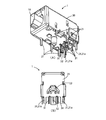
- FIG. 1 is an exploded perspective view of a connector showing a perspective view in FIG. 1. It is the perspective view (A) which showed the connector of this embodiment in the direction which the lower surface appears, and the rear view (B) of the connector of this embodiment. It is a cross-sectional view (A) and a cross-sectional perspective view (B) along the arrow AA shown in FIG. It is a figure which showed the experimental result. It is a figure which showed the experimental result. It is a figure which showed the modification of the inner shell.
- FIG. 1 is a perspective view of a connector according to an embodiment of the present invention.
- This connector 1 is a connector that fits with the mating cottage with the front indicated by the arrow F facing the mating connector (not shown). Further, the connector 1 is mounted on a circuit board (not shown) arranged below indicated by an arrow Z and soldered to the circuit board.
- FIG. 2 is an exploded perspective view of the connector whose perspective view is shown in FIG. 1.
- This connector 1 includes an outer housing 10 and an outer shell 20.
- a storage space 11 is formed in the outer housing 10.
- This accommodation space has openings formed in the front surface facing the mating connector side (facing the direction of the arrow F) and the back facing the mating connector.
- the outer housing 10 corresponds to an example of the housing according to the present invention.
- the outer shell 20 is for a shield and has a shape that covers the upper surface, the left and right side surfaces, and the back surface of the outer housing 10.
- the outer shell 20 is provided with a plurality of pin-shaped solder connection portions 21 that extend downward and are solder-connected to the circuit board.
- this connector 1 includes a front shell 30, a front housing 40, a pin 50, a back housing 60, and a back shell 70.
- the pin 50 has a first extension portion 51 extending back and forth, and a second extension portion 52 extending downward from the rear end of the first extension portion 51.
- the first extension portion 51 comes into contact with the contact of the mating connector fitted to the connector 1 and electrically conducts. Further, the second extension portion 52 is solder-connected to the circuit board arranged below.
- the pin 50 corresponds to an example of a contact according to the present invention.
- front housing 40 and the back housing 60 support the pin 50 so as to sandwich the pin 50 from the front and the rear.
- the front housing 40 and the back housing 60 in the present embodiment have a configuration in which they are combined corresponds to an example of the inner housing referred to in the present invention.
- the front shell 30 and the back shell 70 cover the pin 50 with the front housing 40 and the back housing 60 sandwiched between them, and shield the pin 50.
- the front shell 30 is formed with six pin-shaped solder connection portions 31 that extend downward and are solder-connected to the circuit board.
- the configuration in which the front shell 30 and the back shell 70 are combined corresponds to an example of the inner shell referred to in the present invention.
- an assembly including a front shell 30, a front housing 40, a pin 50, a back housing 60, and a back shell 70 is referred to as a "sub-assembly 80".
- the sub-assembly 80 is loaded into the main housing 10 from the back side of the main housing 10.
- the sub-assembly 80 is inserted into the main housing 10 and the outer shell 20 is covered with the sub-assembly 80 to complete the connector 1 shown in FIG.
- FIG. 3 is a perspective view (A) showing the connector of the present embodiment in a direction in which the lower surface thereof appears, and a rear view (B) of the connector of the present embodiment.
- FIG. 3A shows a second extension portion 52 of the pin 50, a plurality of solder connection portions 21 of the outer shell 20, and a plurality of (six) solder connection portions 31 of the front shell 30.
- the second extension 52 of the pin 50 which is composed of only one, is for signal transmission.
- the other plurality of solder connection portions 21 of the outer shell 20 and the six solder connection portions 31 of the front shell 30 are for fixing the connector 1 to the circuit board and electrically for grounding. ..
- eight of the two solder connection portions 21a at the rear end of the plurality of solder connection portions 21 of the outer shell 20 and the six solder connection portions 31 of the front shell 30 play a role. Is responsible for.
- These eight solder connection portions 21a and 31 are arranged so as to surround the second extension portion 52 of the pin 50.
- FIG. 3B shows a raised piece 22 which is a feature of the present embodiment.
- the raised piece 22 corresponds to an example of the spring portion and an example of the raised piece as referred to in the present invention.
- the raised piece 22 is provided in a region of the outer shell 20 facing the back surface of the outer housing 10, and has a shape cut forward, that is, in the direction of the arrow F shown in FIGS. 1 and 2. The operation of the cut piece 22 will be described below with reference to FIG.
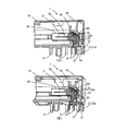
- FIG. 4 is a cross-sectional view (A) and a cross-sectional perspective view (B) of the connector of the present embodiment along the arrows AA shown in FIG.
- the cut-up piece 22 is cut up at an angle of 45 ° with respect to the vertical direction so as to fall forward (in the direction of the arrow F shown in FIGS. 1 and 2).
- the tip 22a of the raised piece 22 abuts on the back shell 70.
- the cut-up piece 22 is shown to bite into the back shell 70, because the shape before deformation in design is shown as it is.
- the raised piece 22 abuts against the back shell 70 and is elastically deformed, pushing the back shell 70 forward (in the direction of arrow F).
- the back shell 70 is pushed by the raised piece 22 and is in contact with the front shell 30 so as not to form a slight gap between the back shell 70 and the front shell 30.
- the raised piece 22 is in contact with the back shell 70 at a position below the first extension 51 extending in the front-rear direction of the pin 50 in the vertical direction. Since the second extension 52 of the pin 50 extends downward from the first extension 51, the back shell 70 also extends far below the first extension 51, and the center of gravity of the back shell 70 is the first. It is located below the extension 51. Therefore, the cut-up piece 22 is brought into contact with the back shell 70 at a position below the first extension portion 51, so that the entire back shell 70 is pressed against the front shell 30 in a well-balanced manner.
- the spring portion referred to in the present invention is realized with a simple structure.
- 5 and 6 are diagrams showing the experimental results.
- FIGS. 5 and 6 are diagram showing the front shell 30 and the back shell 70 in a state where the back shell 70 is in contact with the front shell 30, and is one of the present inventions. Corresponds to the embodiment. On the other hand, in both FIGS. 5 and 6, in FIG. 6, there is no raised piece 22 (see FIGS. 3 and 4), and a slight gap G is provided between the back shell 70 and the front shell 30. It is a figure which showed the front shell 30 and the back shell 70 in the state which was formed.
- This (B) corresponds to a comparative example with respect to the present invention.
- FIG. 5C is a diagram showing the measurement result of the insertion loss (dB).
- the insertion loss (dB) should be close to 0 dB, and in the example in which the back shell 70 is in contact with the front shell 30, the high frequency region of 2.0 to 3.0 GHz is particularly higher than in the non-contact comparative example. Is good at.
- FIG. 5D is a diagram showing the measurement result of the voltage standing wave ratio (VSWR) on the circuit board side.
- the voltage standing wave ratio (VSWR) should be close to 1, and the embodiment of (A) is particularly better in the high frequency region.
- FIG. 6C is a diagram showing the measurement result of the impedance on the circuit board side.
- FIG. 6 (D) is a diagram showing the measurement results of the screening attenuation characteristics.
- the connector 1 of the present embodiment is cut up from the outer shell 20 to form a piece 22, and the back shell 70 is pushed forward to press the back shell 70 against the front shell 0.
- the connector 1 of the present embodiment realizes better signal transmission characteristics as compared with the case where the cut-up piece 22 does not exist.
- the raised piece 22 is cut at an angle of 45 ° with respect to the vertical direction.
- the raised piece 22 does not necessarily have to be cut at an angle of 45 °.
- the raised piece 22 may be cut at an angle smaller than 45 ° with respect to the vertical direction.
- the raised piece 22 is in contact with the back shell 70 at a position of the pin 50 where the second extension 52 extending up and down is present in the height direction.
- the cut piece 22 is cut at an angle smaller than 45 °, it is closer to parallel to the second extension 52 of the pin 50 than when it is cut at an angle of 45 °. Therefore, further improvement of signal transmission characteristics can be expected accordingly.
- the cut piece 22 may be cut at an angle larger than 45 °.
- the spring force can be increased and the back shell 70 can be strongly pushed as compared with the case where the cut piece 22 is cut at an angle of 45 °. Therefore, the back shell 70 can be strongly pressed against the front shell 30 by that amount, and the back shell 70 and the front shell 30 can be brought into close contact with each other more firmly.
- the outer shell 20 is provided with a raised piece 22.
- the raised piece 22 is a cut piece that is cut diagonally toward the front and elastically bends in contact with the back shell 70.
- a cut-up piece provided in the back shell 70 which is cut and raised backward and elastically bends in contact with the outer shell 20, may be provided.
- the back shell 70 can be elastically pressed against the front shell 30.
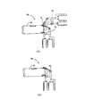
- FIG. 7 is a diagram showing a modified example of the inner shell.
- the parts corresponding to the front shell and the back shell in the above embodiment of the inner shell 90 are referred to as the front shell 30 and the back shell 70 as they are.
- the inner shell 90 has a front shell 30 and a back shell 70 which are partially connected to each other. In this way, by using the inner shell 90 having the front shell 30 and the back shell 70 having a partially connected structure, the number of parts is reduced as compared with the case where they are separated from each other, which is advantageous in terms of assembling and cost. Will be.
- the back shell 70 is kept in an open posture with respect to the front shell 30 as shown by the alternate long and short dash line in FIG. 7 (A). Then, after the contact 50 and the inner housing (front housing 40 and back housing 60) are loaded, the back shell 70 is in the posture shown by the solid line in FIG. 7 (A). When the back shell 70 is kept in the posture shown by this solid line, a gap G tends to remain formed between the front shell 30 and the back shell 70.
- the back shell 70 is pressed forward by the cut-up piece 22 (see FIGS. 3 and 4), whereby the back shell 70 is pressed against the front shell 30.
- FIG. 7B shows the inner shell 90 in this pressed state.
Landscapes
- Details Of Connecting Devices For Male And Female Coupling (AREA)
- Coupling Device And Connection With Printed Circuit (AREA)
Abstract
高周波の広い帯域に亘る良好な伝送特性を有するコネクタを提供する。 コネクタ1は、アウタハウジング10、アウタシェル20、フロントシェル30、フロントハウジング40、ピン50、バックハウジング60、およびバックシェル70を備えている。ここで、アウタシェル20の、アウタハウジング10の背面に沿って広がる部分に、切起し片22が形成されている。この切起し片22は、バックシェル70に当接して弾性的に撓む。これにより、バックシェル70がフロントシェル30に、それらの間に隙間が形成されないように押し当てられる。この押当てにより、バックシェル70とフロントシェル30が電気的に一体化し、良好な信号伝送特性が実現する。
Description
本発明は、高周波信号の伝送に適したコネクタに関する。
高周波信号の伝送では信号の反射等が生じやすく、如何にして良好な伝送特性を実現するかが問題となる。特に、映像信号の伝送には、高周波の広い帯域に亘る良好な伝送特性が要求される。
ここで、特許文献1には、複数の同軸ケーブルがまとめられたフラット同軸ケーブル端をまとめて共通導電部材を介して、回路接地及びフレーム接地に接続する発明が開示されている。この特許文献1の発明は、接地側配線の電位変動の発生及びインピーダンス不連続の発生を無くすることを目的としている。
本発明は、高周波の広い帯域に亘る良好な伝送特性を有するコネクタを提供することを目的とする。
上記目的を達成する本発明のコネクタは、
相手コネクタ側を向いた前面と相手コネクタに背を向けた背面とに開口を有する収容空間が形成されたハウジングと、
ハウジングを、そのハウジングの背面を含んで覆うアウタシェルと、
相手コネクタとの導通を担う、上記収容空間に収容されたコンタクトと、
上記収容空間に配置され、コンタクトを覆うインナシェルとを備え、
アウタシェルの、ハウジングの背面に沿って広がる部分とインナシェルとの間に、インナシェルを前方に向けて弾性的に押圧するバネ部を有することを特徴とする。
相手コネクタ側を向いた前面と相手コネクタに背を向けた背面とに開口を有する収容空間が形成されたハウジングと、
ハウジングを、そのハウジングの背面を含んで覆うアウタシェルと、
相手コネクタとの導通を担う、上記収容空間に収容されたコンタクトと、
上記収容空間に配置され、コンタクトを覆うインナシェルとを備え、
アウタシェルの、ハウジングの背面に沿って広がる部分とインナシェルとの間に、インナシェルを前方に向けて弾性的に押圧するバネ部を有することを特徴とする。
インナシェルは、コンタクトを内側に配置させてそのコンタクトを覆う必要上、複数の部分に分離しているか、あるいは1つに繋がっていても部分的に分離した構造とすることが考えられる。この場合、インナシェルは、押圧がないときに部分的に隙間が形成されあるいは十分には接触していない部分が形成されるおそれがある。
ここで、本発明のコネクタでは、上記のバネ部を有し、インナシェルが前方に向けて弾性的に押圧される。したがって、押圧がないときに隙間が形成されあるいは十分には接触していない部分が形成される構造のインナシェルであっても、その隙間が埋められ、あるいは十分な接触が得られて、高周波の広い帯域に亘る良好な伝送特性が実現する。
ここで、本発明のコネクタにおいて、インナシェルが、互いに分離しあるいは部分的に連結し、コンタクトを前方および後方から挟むように覆うフロントシェルおよびバックシェルを有することが好ましい。
インナシェルを、このような、互いに分離しあるいは部分的に連結した構造とすること
によって、コンタクトを前方および後方から挟むように覆うことができる。
によって、コンタクトを前方および後方から挟むように覆うことができる。
また、本発明のコネクタにおいて、上記バネ部が、アウタシェルに設けられた、前方に向かって斜めに切り起され、インナシェルに当接して弾性的に撓む切起し片であることが好ましい。
バネ部として、インナシェルに設けられて後方に向って切り起され、アウタシェルに当接して弾性的に撓む切起し片を備えてもよい。この構成の場合も、インナシェルを前方に弾性的に押圧することが可能である。ただし、切起し片をインナシェルに備えるよりもアウタシェルに備えたほうが、信号伝送特性上有利と考えられる。したがって、切起し片をアウタシェルに備えるほうが、より好ましい。
また、アウタシェルに設けるかインナシェルに設けるかにかかわらず、このような切起し片を備えることにより、簡易な構造でバネ部を構成することができる。
また、本発明のコネクタにおいて、
コンタクトが、前後に延び相手コネクタとの導通を担う第1延長部と、第1延長部の後端から、回路基板が配置される下方に折れ曲がって延び、回路基板に接続される第2延長部とを有し、
上記の切起し片が、上下方向について、第1延長部よりも下方の位置で、インナシェルに当接していることが好ましい。
コンタクトが、前後に延び相手コネクタとの導通を担う第1延長部と、第1延長部の後端から、回路基板が配置される下方に折れ曲がって延び、回路基板に接続される第2延長部とを有し、
上記の切起し片が、上下方向について、第1延長部よりも下方の位置で、インナシェルに当接していることが好ましい。
コンタクトは、前後に延びる第1延長部と下方に延びる第2延長部とを有し、インナシェルも、下方に延びる形状のコンタクトを覆う形状となっている。このため、インナシェルの上下方向の重心位置は第1延長部よりも下方の位置にある。そこで、上下方向について第1延長部よりも下方の位置で切起し片を当接させるほうが、第1延長部と同一高さあるいは上方の位置で当接させるよりも、インナシェルの全体をバランスよく、前方に押圧することができる。
ここで、上記切起し片が、上下方向に対し45°の角度に切り起されていることが好ましい。
この場合、良好な信号伝送特性とインナシェルへの十分な押圧力の確保とのバランスが保たれる。
あるいは、上記切起し片が、上下方向に対し45°よりも小さい角度に切り起されていることも好ましい態様である。
切起し片は、コンタクトの、上下に延びる第2延長部が存在する高さ位置においてインナシェルに当接している。切起し片は、上下方向に対し45°よりも小さい角度に切り起されている場合、45°の角度に切り起されている場合と比べ、コンタクトの第2延長部と平行に近づく。したがって、その分、信号伝送特性の更なる向上に寄与する。
あるいは、切起し片が、上下方向に対し45°よりも大きい角度に切り起されていることも好ましい態様である。
切起し片が、上下方向に対し45°よりも大きい角度に切り起されている場合、45°の角度に切り起されている場合と比べ、インナシェルを強く押圧することができる。したがって、その分、インナシェルに形成されている隙間あるいは不十分な接触が一層確実に解消され、インナシェルをさらに強固に一体化させることができる。
また、本発明のコネクタにおいて、
上記収容空間に配置され、コンタクトを支持するインナハウジングを備え、
インナシェルが、インナハウジングを間に挟んでコンタクトを覆うことが好ましい。
上記収容空間に配置され、コンタクトを支持するインナハウジングを備え、
インナシェルが、インナハウジングを間に挟んでコンタクトを覆うことが好ましい。
上記のインナハウジングを備えることにより、コンタクトの位置ずれ等が生じにくい、一層強固なコネクタが実現する。
図1は、本発明の一実施形態のコネクタの斜視図である。
このコネクタ1は、矢印Fで示す前方を相手コネクタ(不図示)に向けて、その相手コケクタと嵌合するコネクタである。また、このコネクタ1は、矢印Zで示す下方に配置された回路基板(不図示)に搭載されてその回路基板に半田付けされる。
図2は、図1に斜視図を示すコネクタの分解斜視図である。
このコネクタ1は、アウタハウジング10およびアウタシェル20を備えている。
アウタハウジング10には、収容空間11が形成されている。この収容空間は相手コネクタ側を向いた(矢印Fの向きを向いた)前面と相手コネクタに背を向けた背面とに開口が形成されている。このアウタハウジング10は、本発明にいうハウジングの一例に相当する。
また、アウタシェル20は、シールド用であって、アウタハウジング10の上面と、左右の側面と、背面とを覆う形状を有する。このアウタシェル20には、下方に延びて回路基板に半田接続されるピン形状の複数の半田接続部21が設けられている。
また、このコネクタ1は、フロントシェル30、フロントハウジング40、ピン50、バックハウジング60、およびバックシェル70を備えている。
ピン50は、前後に延びる第1延長部51と、その第1延長部51の後端から下方に折れ曲がって延びる第2延長部52とを有する。第1延長部51は、このコネクタ1に嵌合する相手コネクタのコンタクトと接触して電気的に導通する。また、第2延長部52は、下方に配置される回路基板に半田接続される。このピン50は、本発明にいうコンタクトの一例に相当する。
また、フロントハウジング40およびバックハウジング60は、ピン50を前方および後方から挟むように支持する。本実施形態におけるフロントハウジング40およびバックハウジング60は、それらを合わせた構成が、本発明にいうインナハウジングの一例に相
当する。
当する。
さらに、フロントシェル30およびバックシェル70は、フロントハウジング40およびバックハウジング60を間に挟んでピン50を覆い、このピン50をシールドする。フロントシェル30には、下方に延びて回路基板に半田接続されるピン形状の6本の半田接続部31が形成されている。本実施形態では、これらフロントシェル30およびバックシェル70を合わせた構成が、本発明にいうインナシェルの一例に相当する。
ここでは、フロントシェル30、フロントハウジング40、ピン50、バックハウジング60、およびバックシェル70からなる組立体を、「副組立体80」と称する。この副組立体80は、メインハウジング10の背面側からそのメインハウジング10内に装入される。メインハウジング10に副組立体80が挿入され、アウタシェル20が被せられて、図1に示すコネクタ1が完成する。
図3は、本実施形態のコネクタを、その下面が現れる向きに示した斜視図(A)、および本実施形態のコネクタの背面図(B)である。
図3(A)には、ピン50の第2延長部52、アウタシェル20の複数の半田接続部21、およびフロントシェル30の複数(6本)の半田接続部31が示されている。これらのうち、1本のみからなるピン50の第2延長部52は信号伝送用である。その他の、アウタシェル20の複数の半田接続部21およびフロントシェル30の6本の半田接続部31は、このコネクタ1の、回路基板への固定用であり、また、電気的には接地用である。接地用としては、特に、アウタシェル20の複数の半田接続部21のうちの後端の2本の半田接続部21aと、フロントシェル30の6本の半田接続部31との8本が、その役割を担っている。これら8本の半田接続部21a,31は、ピン50の第2延長部52を取り巻くように配置されている。
また、図3(B)には、本実施形態の特徴である切起し片22が示されている。この切起し片22は、本発明にいう、バネ部の一例および切起し片の一例に相当する。この切起し片22は、アウタシェル20の、アウタハウジング10の背面に面する領域に設けられ、前方、すなわち図1,図2に示す矢印Fの向きに切り起された形状を有する。切起し片
22の作用については、以下、図4を参照しながら説明する。
22の作用については、以下、図4を参照しながら説明する。
図4は、本実施形態のコネクタの、図1に示す矢印A-Aに沿う断面図(A)と断面斜視図(B)である。
切起し片22は、前方(図1,図2に示す矢印Fの向き)に倒れるように、本実施形態では上下方向に対し45°の角度に切り起されている。そして、この切起し片22の先端部22aは、バックシェル70に突き当たっている。図4では、切起し片22がバックシェル70に食い込んでいるように示されているが、これは、設計上の変形前の形状をそのまま示しているためである。実際には、切起し片22はバックシェル70に突き当たって弾性的に変形し、バックシェル70を前方(矢印Fの向き)に押している。バックシェル70は、その切起し片22に押されて、フロントシェル30との間にわずかな隙間も生じないようにフロントシェル30に当接している。
ここで、切起し片22は、上下方向について、ピン50の、前後に延びる第1延長部51よりも下方の位置で、バックシェル70に当接している。ピン50の第2延長部52が第1延長部51から下に延びているため、バックシェル70も、第1延長部51よりも下側に大きく広がっていて、バックシェル70の重心は第1延長部51よりも下側に位置している。したがって、切起し片22を、バックシェル70に、第1延長部51よりも下方
の位置で当接させることにより、バックシェル70の全体をバランスよく、フロントシェル30に押し当てている。
の位置で当接させることにより、バックシェル70の全体をバランスよく、フロントシェル30に押し当てている。
本実施形態では、このような切起し片22を形成することにより、本発明にいうバネ部を簡易な構造で実現している。
図5、図6は、実験結果を示した図である。
ここで、図5、図6のいずれにおいても、(A)は、バックシェル70がフロントシェル30に突き当った状態にあるフロントシェル30とバックシェル70を示した図であり、本発明の一実施例に相当する。一方、図5、図6のいずれにおいても、(B)は、切起し片22(図3,図4参照)が存在せず、バックシェル70とフロントシェル30との間にわずかな隙間Gが形成された状態にあるフロントシェル30とバックシェル70を示した図である。この(B)は、本発明に対する比較例に相当する。
図5(C)は、挿入損失(dB)の測定結果を示した図である。
挿入損失(dB)は、0dBに近いほうが良く、バックシェル70がフロントシェル30に接触している実施例の方が、非接触の比較例と比べ、特に2.0~3.0GHzという高周波領域において良好である。
また、図5(D)は、回路基板側の電圧定在波比(VSWR)の測定結果を示した図である。
電圧定在波比(VSWR)は、1に近いほうが良く、特に高周波領域において、(A)の実施例の方が良好である。
また、図6(C)は、回路基板側のインピーダンスの測定結果を示した図である。
インピーダンスは常に50ohmで安定しているほうが良く、このインピーダンスに関しても(A)の実施例の方が良好である。
さらに、図6(D)は、スクリーニング減衰特性の測定結果を示した図である。
スクリーニング減衰特性は低い方が良く、このスクリーニング減衰特性に関しても(A)の実施例の方が良好である。
このように、本実施形態のコネクタ1は、アウタシェル20に切起し片22を形成し、バックシェル70を前方に押してバックシェル70をフロントシェル0に押し当てている。これにより、本実施形態のコネクタ1は、切起し片22が存在しない場合と比べ、良好な信号伝送特性を実現している。
なお、本実施形態では、切起し片22が、上下方向に対し45°の角度に切り起されている。これにより、本実施形態では、信号伝送特性とバックシェル70のフロントシェル30への押当て力の確保とのバランスが保たれている。
ただし、切起し片22は、必ずしも45°の角度に切り起されている必要はない。例えば、この切起し片22は、上下方向に対し45°よりも小さい角度に切り起されていてもよい。切起し片22は、高さ方向について、ピン50の、上下に延びる第2延長部52が存在する位置においてバックシェル70に当接している。切起し片22が、45°よりも
小さい角度に切り起されている場合、45°の角度に切り起されている場合と比べ、ピン50の第2延長部52と平行に近づく。したがって、その分、信号伝送特性の更なる向上が期待できる。
小さい角度に切り起されている場合、45°の角度に切り起されている場合と比べ、ピン50の第2延長部52と平行に近づく。したがって、その分、信号伝送特性の更なる向上が期待できる。
あるいは、切起し片22が、45°よりも大きい角度に切り起されていてもよい。この場合、切起し片22が45°の角度に切り起されている場合と比べ、バネ力を高め、バックシェル70を強く押すことができる。したがって、その分、バックシェル70をフロントシェル30に強く押し当てて、バックシェル70とフロントシェル30をさらに強固に密着させることができる。
また、本実施形態では、アウタシェル20に切起し片22が設けられている。この切起し片22は、前方に向かって斜めに切り起されていて、バックシェル70に当接して弾性的に撓む切起し片である。ただし、この切起し片22に代わり、バックシェル70に設けられて後方に向って切り起され、アウタシェル20に当接して弾性的に撓む切起し片を備えてもよい。この構成の場合も、バックシェル70をフロントシェル30に弾性的に押し当てることが可能である。
図7は、インナシェルの変形例を示した図である。ここでは、理解の容易なため、このインナシェル90の、上記の実施形態におけるフロントシェルおよびバックシェルに相当する部分について、そのまま、フロントシェル30およびバックシェル70と称する。
この図7に示す構造のインナシェル90を採用した場合であっても、このインナシェル90以外の各部の構造は、上述の実施形態のものがそのまま踏襲される。
このインナシェル90は、一部が互いに連結したフロントシェル30とバックシェル70とを有する。このように、部分的に連結した構造のフロントシェル30とバックシェル70とを有するインナシェル90とすることにより、互いに分離している場合と比べ、部品点数が削減され、組立性やコスト上有利となる。
このインナシェル90の内部には、コンタクト50、並びに、そのコンタクト50を支持する、フロントハウジング40およびバックハウジング60からなるインナハウジングを装入する必要がある。そこで、その装入の時点では、バックシェル70を、フロントシェル30に対し、図7(A)に一点鎖線で示すように開いた姿勢にしておく。そして、コンタクト50およびインナハウジング(フロントハウジング40およびバックハウジング60)を装入した後、バックシェル70を、図7(A)に実線で示す姿勢とする。バックシェル70をこの実線で示す姿勢にしたままでは、フロントシェル30とバックシェル70との間に隙間Gが形成されたままとなりがちである。
切起し片22(図3、図4参照)によってバックシェル70が前方に押圧され、これにより、バックシェル70がフロントシェル30に押し当てられる。図7(B)には、この押し当てられた状態のインナシェル90が示されている。この押し当てによりフロントシェル30とバックシェル70が電気的に一体化され、図5、図6に示したような良好な信号伝送特性を得ることができる。
1 コネクタ
10 アウタハウジング
11 収容空間
20 アウタシェル
21,21a 半田接続部
22 切起し片
22a 切起し片の先端部
30 フロントシェル
31 半田接続部
40 フロントハウジング
50 ピン
51 第1延長部
52 第2延長部
60 バックハウジング
70 バックシェル
80 副組立体
90 インナシェル
10 アウタハウジング
11 収容空間
20 アウタシェル
21,21a 半田接続部
22 切起し片
22a 切起し片の先端部
30 フロントシェル
31 半田接続部
40 フロントハウジング
50 ピン
51 第1延長部
52 第2延長部
60 バックハウジング
70 バックシェル
80 副組立体
90 インナシェル
Claims (8)
- 相手コネクタ側を向いた前面と相手コネクタに背を向けた背面とに開口を有する収容空間が形成されたハウジングと、
前記ハウジングを、該ハウジングの背面を含んで覆うアウタシェルと、
相手コネクタとの導通を担う、前記収容空間に収容されたコンタクトと、
前記収容空間に配置され、前記コンタクトを覆うインナシェルとを備え、
前記アウタシェルの、前記ハウジングの背面に沿って広がる部分と前記インナシェルと
の間に、該インナシェルを前方に向けて弾性的に押圧するバネ部を有することを特徴とするコネクタ。 - 前記インナシェルが、互いに分離しあるいは部分的に連結し、コンタクトを前方および後方から挟むように覆うフロントシェルおよびバックシェルを有することを特徴とする請求項1に記載のコネクタ。
- 前記バネ部が、前記アウタシェルに設けられた、前方に向かって斜めに切り起され、前記インナシェルに当接して弾性的に撓む切起し片であることを特徴とする請求項1または2に記載のコネクタ。
- 前記コンタクトが、前後に延び相手コネクタとの導通を担う第1延長部と、該第1延長部の後端から、回路基板が配置される下方に折れ曲がって延び、該回路基板に接続される第2延長部とを有し、
前記切起し片が、上下方向について、前記第1延長部よりも下方の位置で、前記バックシェルに当接していることを特徴とする請求項3に記載のコネクタ。 - 前記切起し片が、上下方向に対し45°の角度に切り起されていることを特徴とする請求項4に記載のコネクタ。
- 前記切起し片が、上下方向に対し45°よりも小さい角度に切り起されていることを特徴とする請求項4に記載のコネクタ。
- 前記切起し片が、上下方向に対し45°よりも大きい角度に切り起されていることを特徴とする請求項4に記載のコネクタ。
- 前記収容空間に配置され、前記コンタクトを支持するインナハウジングを備え、
前記インナシェルが、前記インナハウジングを間に挟んで前記コンタクトを覆うことを特徴する請求項1から7のうちのいずれか1項に記載のコネクタ。
Priority Applications (4)
| Application Number | Priority Date | Filing Date | Title |
|---|---|---|---|
| EP21832088.5A EP4178044A4 (en) | 2020-07-03 | 2021-06-18 | Connector |
| CN202180047119.2A CN115735304B (zh) | 2020-07-03 | 2021-06-18 | 连接器 |
| KR1020237003834A KR20230028559A (ko) | 2020-07-03 | 2021-06-18 | 커넥터 |
| US18/148,750 US20230142379A1 (en) | 2020-07-03 | 2022-12-30 | Connector |
Applications Claiming Priority (2)
| Application Number | Priority Date | Filing Date | Title |
|---|---|---|---|
| JP2020-115360 | 2020-07-03 | ||
| JP2020115360A JP7479967B2 (ja) | 2020-07-03 | 2020-07-03 | コネクタ |
Related Child Applications (1)
| Application Number | Title | Priority Date | Filing Date |
|---|---|---|---|
| US18/148,750 Continuation US20230142379A1 (en) | 2020-07-03 | 2022-12-30 | Connector |
Publications (1)
| Publication Number | Publication Date |
|---|---|
| WO2022004438A1 true WO2022004438A1 (ja) | 2022-01-06 |
Family
ID=79316155
Family Applications (1)
| Application Number | Title | Priority Date | Filing Date |
|---|---|---|---|
| PCT/JP2021/023259 Ceased WO2022004438A1 (ja) | 2020-07-03 | 2021-06-18 | コネクタ |
Country Status (6)
| Country | Link |
|---|---|
| US (1) | US20230142379A1 (ja) |
| EP (1) | EP4178044A4 (ja) |
| JP (1) | JP7479967B2 (ja) |
| KR (1) | KR20230028559A (ja) |
| CN (1) | CN115735304B (ja) |
| WO (1) | WO2022004438A1 (ja) |
Cited By (1)
| Publication number | Priority date | Publication date | Assignee | Title |
|---|---|---|---|---|
| WO2024165959A1 (en) * | 2023-02-07 | 2024-08-15 | Te Connectivity Solutions Gmbh | Angled connector |
Citations (4)
| Publication number | Priority date | Publication date | Assignee | Title |
|---|---|---|---|---|
| JP2009043704A (ja) * | 2007-07-18 | 2009-02-26 | Yazaki Corp | シールドコネクタ構造 |
| JP2016207411A (ja) * | 2015-04-21 | 2016-12-08 | 日本航空電子工業株式会社 | コネクタ |
| JP2020013748A (ja) * | 2018-07-20 | 2020-01-23 | 株式会社オートネットワーク技術研究所 | シールドコネクタ及び外導体端子 |
| JP2021034273A (ja) * | 2019-08-27 | 2021-03-01 | 矢崎総業株式会社 | 基板実装型のコネクタ、及び、コネクタ付き基板 |
Family Cites Families (4)
| Publication number | Priority date | Publication date | Assignee | Title |
|---|---|---|---|---|
| JPH08222325A (ja) | 1995-02-13 | 1996-08-30 | Fujitsu Ltd | プリント配線板へのフラット同軸ケーブルの接続法 |
| JP5836715B2 (ja) * | 2011-09-07 | 2015-12-24 | 矢崎総業株式会社 | シールドコネクタ |
| JP2017045604A (ja) * | 2015-08-26 | 2017-03-02 | タイコエレクトロニクスジャパン合同会社 | シールドコネクタ |
| JP2020043024A (ja) * | 2018-09-13 | 2020-03-19 | 矢崎総業株式会社 | 基板用コネクタ |
-
2020
- 2020-07-03 JP JP2020115360A patent/JP7479967B2/ja active Active
-
2021
- 2021-06-18 WO PCT/JP2021/023259 patent/WO2022004438A1/ja not_active Ceased
- 2021-06-18 EP EP21832088.5A patent/EP4178044A4/en active Pending
- 2021-06-18 KR KR1020237003834A patent/KR20230028559A/ko not_active Withdrawn
- 2021-06-18 CN CN202180047119.2A patent/CN115735304B/zh active Active
-
2022
- 2022-12-30 US US18/148,750 patent/US20230142379A1/en active Pending
Patent Citations (4)
| Publication number | Priority date | Publication date | Assignee | Title |
|---|---|---|---|---|
| JP2009043704A (ja) * | 2007-07-18 | 2009-02-26 | Yazaki Corp | シールドコネクタ構造 |
| JP2016207411A (ja) * | 2015-04-21 | 2016-12-08 | 日本航空電子工業株式会社 | コネクタ |
| JP2020013748A (ja) * | 2018-07-20 | 2020-01-23 | 株式会社オートネットワーク技術研究所 | シールドコネクタ及び外導体端子 |
| JP2021034273A (ja) * | 2019-08-27 | 2021-03-01 | 矢崎総業株式会社 | 基板実装型のコネクタ、及び、コネクタ付き基板 |
Non-Patent Citations (1)
| Title |
|---|
| See also references of EP4178044A4 * |
Cited By (2)
| Publication number | Priority date | Publication date | Assignee | Title |
|---|---|---|---|---|
| WO2024165959A1 (en) * | 2023-02-07 | 2024-08-15 | Te Connectivity Solutions Gmbh | Angled connector |
| US12586959B2 (en) | 2023-02-07 | 2026-03-24 | Te Connectivity Solutions Gmbh | Angled connector |
Also Published As
| Publication number | Publication date |
|---|---|
| CN115735304A (zh) | 2023-03-03 |
| KR20230028559A (ko) | 2023-02-28 |
| JP2022022734A (ja) | 2022-02-07 |
| CN115735304B (zh) | 2026-05-01 |
| US20230142379A1 (en) | 2023-05-11 |
| JP7479967B2 (ja) | 2024-05-09 |
| EP4178044A4 (en) | 2024-07-31 |
| EP4178044A1 (en) | 2023-05-10 |
Similar Documents
| Publication | Publication Date | Title |
|---|---|---|
| US9680260B2 (en) | Cable connector assembly with improved grounding structure | |
| US9825407B2 (en) | Cable connector assembly having improved metal shell | |
| JP7032978B2 (ja) | L形同軸端子を備えたコネクタおよびその製造方法 | |
| KR101026650B1 (ko) | 전기 커넥터 | |
| JP7446094B2 (ja) | 接続対象物、コネクタ、及びハーネス | |
| JP2011171129A (ja) | 電気コネクタ及び電気コネクタ組立体 | |
| US6945824B1 (en) | Connector assembly | |
| JP7023499B2 (ja) | 電気コネクタ | |
| JP4705102B2 (ja) | コネクタ、回路基板及び電子機器 | |
| JP2021096960A (ja) | 電気コネクタ及び電気コネクタ装置 | |
| JP2008016212A (ja) | 電気コネクタ | |
| US12451651B2 (en) | Connector | |
| WO2011086857A1 (ja) | 電気コネクタ及び電気コネクタ組立体 | |
| JP7112062B2 (ja) | 電気コネクタ | |
| US11050194B2 (en) | Connector | |
| US20230142379A1 (en) | Connector | |
| CN102570211A (zh) | 用于跨装式连接器的安装特征 | |
| JP2010113813A (ja) | 電気コネクタ | |
| US7309237B2 (en) | Micro coaxial cable connector assembly with grounding mechanism | |
| US7445470B2 (en) | Electrical connector with improved housing | |
| US20230307870A1 (en) | Electrical connector assembly having improved locking elements | |
| JP7468657B2 (ja) | 第1コネクタ、第2コネクタ、及びコネクタセット | |
| US7318753B2 (en) | Electrical jack with improved grounding contact | |
| JP7563342B2 (ja) | 電気コネクタ | |
| JP2015219987A (ja) | シールドコネクタ |
Legal Events
| Date | Code | Title | Description |
|---|---|---|---|
| 121 | Ep: the epo has been informed by wipo that ep was designated in this application |
Ref document number: 21832088 Country of ref document: EP Kind code of ref document: A1 |
|
| ENP | Entry into the national phase |
Ref document number: 20237003834 Country of ref document: KR Kind code of ref document: A |
|
| WWE | Wipo information: entry into national phase |
Ref document number: 2021832088 Country of ref document: EP |
|
| NENP | Non-entry into the national phase |
Ref country code: DE |