WO2022004676A1 - コイル、送電装置及び受電装置並びに電力伝送システム - Google Patents
コイル、送電装置及び受電装置並びに電力伝送システム Download PDFInfo
- Publication number
- WO2022004676A1 WO2022004676A1 PCT/JP2021/024417 JP2021024417W WO2022004676A1 WO 2022004676 A1 WO2022004676 A1 WO 2022004676A1 JP 2021024417 W JP2021024417 W JP 2021024417W WO 2022004676 A1 WO2022004676 A1 WO 2022004676A1
- Authority
- WO
- WIPO (PCT)
- Prior art keywords
- coil
- power transmission
- thin film
- winding
- copper thin
- Prior art date
- Legal status (The legal status is an assumption and is not a legal conclusion. Google has not performed a legal analysis and makes no representation as to the accuracy of the status listed.)
- Ceased
Links
Images










Classifications
-
- H—ELECTRICITY
- H02—GENERATION; CONVERSION OR DISTRIBUTION OF ELECTRIC POWER
- H02J—ELECTRIC POWER NETWORKS; CIRCUIT ARRANGEMENTS OR SYSTEMS FOR SUPPLYING OR DISTRIBUTING ELECTRIC POWER; SYSTEMS FOR STORING ELECTRIC ENERGY
- H02J50/00—Circuit arrangements or systems for wireless supply or distribution of electric power
- H02J50/10—Circuit arrangements or systems for wireless supply or distribution of electric power using inductive coupling
-
- H—ELECTRICITY
- H01—ELECTRIC ELEMENTS
- H01F—MAGNETS; INDUCTANCES; TRANSFORMERS; SELECTION OF MATERIALS FOR THEIR MAGNETIC PROPERTIES
- H01F38/00—Adaptations of transformers or inductances for specific applications or functions
- H01F38/14—Inductive couplings
-
- B—PERFORMING OPERATIONS; TRANSPORTING
- B60—VEHICLES IN GENERAL
- B60L—PROPULSION OF ELECTRICALLY-PROPELLED VEHICLES; SUPPLYING ELECTRIC POWER FOR AUXILIARY EQUIPMENT OF ELECTRICALLY-PROPELLED VEHICLES; ELECTRODYNAMIC BRAKE SYSTEMS FOR VEHICLES IN GENERAL; MAGNETIC SUSPENSION OR LEVITATION FOR VEHICLES; MONITORING OPERATING VARIABLES OF ELECTRICALLY-PROPELLED VEHICLES; ELECTRIC SAFETY DEVICES FOR ELECTRICALLY-PROPELLED VEHICLES
- B60L53/00—Methods of charging batteries, specially adapted for electric vehicles; Charging stations or on-board charging equipment therefor; Exchange of energy storage elements in electric vehicles
- B60L53/10—Methods of charging batteries, specially adapted for electric vehicles; Charging stations or on-board charging equipment therefor; Exchange of energy storage elements in electric vehicles characterised by the energy transfer between the charging station and the vehicle
- B60L53/12—Inductive energy transfer
-
- B—PERFORMING OPERATIONS; TRANSPORTING
- B60—VEHICLES IN GENERAL
- B60M—POWER SUPPLY LINES, AND DEVICES ALONG RAILS, FOR ELECTRICALLY- PROPELLED VEHICLES
- B60M7/00—Power lines or rails specially adapted for electrically-propelled vehicles of special types, e.g. suspension tramway, ropeway, underground railway
- B60M7/003—Power lines or rails specially adapted for electrically-propelled vehicles of special types, e.g. suspension tramway, ropeway, underground railway for vehicles using stored power (e.g. charging stations)
-
- H—ELECTRICITY
- H01—ELECTRIC ELEMENTS
- H01F—MAGNETS; INDUCTANCES; TRANSFORMERS; SELECTION OF MATERIALS FOR THEIR MAGNETIC PROPERTIES
- H01F27/00—Details of transformers or inductances, in general
- H01F27/28—Coils; Windings; Conductive connections
- H01F27/2804—Printed windings
-
- H—ELECTRICITY
- H01—ELECTRIC ELEMENTS
- H01F—MAGNETS; INDUCTANCES; TRANSFORMERS; SELECTION OF MATERIALS FOR THEIR MAGNETIC PROPERTIES
- H01F27/00—Details of transformers or inductances, in general
- H01F27/34—Special means for preventing or reducing unwanted electric or magnetic effects, e.g. no-load losses, reactive currents, harmonics, oscillations, leakage fields
-
- H—ELECTRICITY
- H01—ELECTRIC ELEMENTS
- H01F—MAGNETS; INDUCTANCES; TRANSFORMERS; SELECTION OF MATERIALS FOR THEIR MAGNETIC PROPERTIES
- H01F27/00—Details of transformers or inductances, in general
- H01F27/34—Special means for preventing or reducing unwanted electric or magnetic effects, e.g. no-load losses, reactive currents, harmonics, oscillations, leakage fields
- H01F27/38—Auxiliary core members; Auxiliary coils or windings
-
- H—ELECTRICITY
- H01—ELECTRIC ELEMENTS
- H01F—MAGNETS; INDUCTANCES; TRANSFORMERS; SELECTION OF MATERIALS FOR THEIR MAGNETIC PROPERTIES
- H01F27/00—Details of transformers or inductances, in general
- H01F27/40—Structural association with built-in electric component, e.g. fuse
-
- H—ELECTRICITY
- H02—GENERATION; CONVERSION OR DISTRIBUTION OF ELECTRIC POWER
- H02J—ELECTRIC POWER NETWORKS; CIRCUIT ARRANGEMENTS OR SYSTEMS FOR SUPPLYING OR DISTRIBUTING ELECTRIC POWER; SYSTEMS FOR STORING ELECTRIC ENERGY
- H02J50/00—Circuit arrangements or systems for wireless supply or distribution of electric power
- H02J50/005—Mechanical details of housing or structure aiming to accommodate the power transfer means, e.g. mechanical integration of coils, antennas or transducers into emitting or receiving devices
-
- H—ELECTRICITY
- H02—GENERATION; CONVERSION OR DISTRIBUTION OF ELECTRIC POWER
- H02J—ELECTRIC POWER NETWORKS; CIRCUIT ARRANGEMENTS OR SYSTEMS FOR SUPPLYING OR DISTRIBUTING ELECTRIC POWER; SYSTEMS FOR STORING ELECTRIC ENERGY
- H02J50/00—Circuit arrangements or systems for wireless supply or distribution of electric power
- H02J50/70—Circuit arrangements or systems for wireless supply or distribution of electric power involving the reduction of electric, magnetic or electromagnetic leakage fields
-
- H—ELECTRICITY
- H01—ELECTRIC ELEMENTS
- H01F—MAGNETS; INDUCTANCES; TRANSFORMERS; SELECTION OF MATERIALS FOR THEIR MAGNETIC PROPERTIES
- H01F27/00—Details of transformers or inductances, in general
- H01F27/28—Coils; Windings; Conductive connections
- H01F27/2804—Printed windings
- H01F2027/2809—Printed windings on stacked layers
-
- H—ELECTRICITY
- H01—ELECTRIC ELEMENTS
- H01F—MAGNETS; INDUCTANCES; TRANSFORMERS; SELECTION OF MATERIALS FOR THEIR MAGNETIC PROPERTIES
- H01F41/00—Apparatus or processes specially adapted for manufacturing or assembling magnets, inductances or transformers; Apparatus or processes specially adapted for manufacturing materials characterised by their magnetic properties
- H01F41/02—Apparatus or processes specially adapted for manufacturing or assembling magnets, inductances or transformers; Apparatus or processes specially adapted for manufacturing materials characterised by their magnetic properties for manufacturing cores, coils, or magnets
- H01F41/04—Apparatus or processes specially adapted for manufacturing or assembling magnets, inductances or transformers; Apparatus or processes specially adapted for manufacturing materials characterised by their magnetic properties for manufacturing cores, coils, or magnets for manufacturing coils
- H01F41/041—Printed circuit coils
- H01F41/042—Printed circuit coils by thin film techniques
-
- H—ELECTRICITY
- H02—GENERATION; CONVERSION OR DISTRIBUTION OF ELECTRIC POWER
- H02J—ELECTRIC POWER NETWORKS; CIRCUIT ARRANGEMENTS OR SYSTEMS FOR SUPPLYING OR DISTRIBUTING ELECTRIC POWER; SYSTEMS FOR STORING ELECTRIC ENERGY
- H02J50/00—Circuit arrangements or systems for wireless supply or distribution of electric power
- H02J50/10—Circuit arrangements or systems for wireless supply or distribution of electric power using inductive coupling
- H02J50/12—Circuit arrangements or systems for wireless supply or distribution of electric power using inductive coupling of the resonant type
-
- Y—GENERAL TAGGING OF NEW TECHNOLOGICAL DEVELOPMENTS; GENERAL TAGGING OF CROSS-SECTIONAL TECHNOLOGIES SPANNING OVER SEVERAL SECTIONS OF THE IPC; TECHNICAL SUBJECTS COVERED BY FORMER USPC CROSS-REFERENCE ART COLLECTIONS [XRACs] AND DIGESTS
- Y02—TECHNOLOGIES OR APPLICATIONS FOR MITIGATION OR ADAPTATION AGAINST CLIMATE CHANGE
- Y02T—CLIMATE CHANGE MITIGATION TECHNOLOGIES RELATED TO TRANSPORTATION
- Y02T10/00—Road transport of goods or passengers
- Y02T10/60—Other road transportation technologies with climate change mitigation effect
- Y02T10/70—Energy storage systems for electromobility, e.g. batteries
-
- Y—GENERAL TAGGING OF NEW TECHNOLOGICAL DEVELOPMENTS; GENERAL TAGGING OF CROSS-SECTIONAL TECHNOLOGIES SPANNING OVER SEVERAL SECTIONS OF THE IPC; TECHNICAL SUBJECTS COVERED BY FORMER USPC CROSS-REFERENCE ART COLLECTIONS [XRACs] AND DIGESTS
- Y02—TECHNOLOGIES OR APPLICATIONS FOR MITIGATION OR ADAPTATION AGAINST CLIMATE CHANGE
- Y02T—CLIMATE CHANGE MITIGATION TECHNOLOGIES RELATED TO TRANSPORTATION
- Y02T10/00—Road transport of goods or passengers
- Y02T10/60—Other road transportation technologies with climate change mitigation effect
- Y02T10/7072—Electromobility specific charging systems or methods for batteries, ultracapacitors, supercapacitors or double-layer capacitors
-
- Y—GENERAL TAGGING OF NEW TECHNOLOGICAL DEVELOPMENTS; GENERAL TAGGING OF CROSS-SECTIONAL TECHNOLOGIES SPANNING OVER SEVERAL SECTIONS OF THE IPC; TECHNICAL SUBJECTS COVERED BY FORMER USPC CROSS-REFERENCE ART COLLECTIONS [XRACs] AND DIGESTS
- Y02—TECHNOLOGIES OR APPLICATIONS FOR MITIGATION OR ADAPTATION AGAINST CLIMATE CHANGE
- Y02T—CLIMATE CHANGE MITIGATION TECHNOLOGIES RELATED TO TRANSPORTATION
- Y02T90/00—Enabling technologies or technologies with a potential or indirect contribution to GHG emissions mitigation
- Y02T90/10—Technologies relating to charging of electric vehicles
- Y02T90/14—Plug-in electric vehicles
Definitions
- the present invention belongs to the technical fields of coils, power transmission devices and power receiving devices, and power transmission systems, and more specifically, coils for non-contact power transmission, non-contact power transmission devices and power receiving devices using the coils, and power receiving devices. It belongs to the technical field of power transmission systems.
- the wireless power transmission method generally includes an electric field coupling method, an electromagnetic induction method, a magnetic field resonance method, and the like.
- Patent Document 1 discloses a coil that transmits power by a magnetic field resonance method using a one-turn (one-turn) loop coil and a five-and-a-half-turn (5.5-turn) open coil. There is.
- the frequency of the electric power transmitted and received by the wireless power transmission is predetermined by law for each device responsible for it, and in the case of electric power transmission to the electric vehicle, it is set to a high frequency of 85 kilohertz.
- a high-frequency current is passed through a conductor, the current density is high on the surface of the conductor and decreases toward the center of the conductor.
- the higher the frequency of the current the more the current concentrates on the surface, and as a result, the AC resistance of the conductor increases. This phenomenon is known as the so-called “skin effect of conductors".
- the AC resistance in the conductor when a high frequency current is passed through the conductor is simply referred to as "impedance".
- the present invention has been made in view of the above problems and requirements, and one example of the problem is to improve the efficiency of wireless power transmission even when a high frequency current such as 85 kilohertz is used. It is an object of the present invention to provide a possible coil, a non-contact type power transmission device and a power receiving device using the coil, and a power transmission system.
- the invention according to claim 1 is a first winding line in which a thin film conductor is wound in a coil for non-contact power transmission, and each of them has a linear shape.
- a first winding line composed of a plurality of first straight line portions, a plurality of first curved portions each connecting the first straight line portions and having a curved shape, and a second winding formed by winding a thin film conductor.
- the insulating layer is composed of a plurality of second straight portions each of which is a winding line and has a linear shape, and a plurality of second curved portions of which the second straight portions are connected to each other and each of which has a curved shape.
- each of the first volume line and the second volume line in a plan view is the same polygon as each other.
- a first winding line having a plurality of first straight lines and a plurality of first curved sections and made of a thin film conductor, a plurality of second straight sections and a plurality of second curved sections. It is composed of a thin film conductor and has a second volume line laminated on the first volume line with an insulating layer interposed therebetween.
- the overall shape of the first volume line and the second volume line in a plan view is the same polygon, and the position seen from the center of at least a part of the coil of each first straight line portion and each first straight line.
- each second straight line portion corresponding to at least a part of the portions as seen from the center of the coil coincide with each other in a plan view. Therefore, it is possible to reduce the AC resistance as a coil due to the so-called skin effect or proximity effect caused by forming a winding line with a thin film conductor for weight reduction and cost reduction, resulting in weight reduction and cost reduction. It is possible to improve the transmission efficiency and prevent the operating temperature from rising at the same time.
- the invention according to claim 2 is the coil according to claim 1, and in the winding of the first winding line, the first one included in one winding.
- the winding transition for one winding is performed only in the curved portion, and in the winding of the second winding line, only one winding portion included in one winding is used for one winding. A winding transition is taking place.
- the invention according to claim 3 describes the position of the first curved portion in the coil according to claim 2 where the winding transition is performed in the first winding line, and the said.
- the position of the second curved portion where the winding transition is performed in the second winding line is configured to be within the same region of the coil as viewed from the center.
- the position of the first curve portion where the winding transition is performed in the first volume line and the winding in the second volume line Since the position of the second curved part where the transition is performed is in the same region as seen from the center of the coil, more positions of the first straight line part and the second straight part seen from the coil center are planes. Can be visually matched.
- the invention according to claim 4 is the coil according to claim 1, and in the winding of the first winding line, the first one included in one winding.
- the winding transition for one winding is performed only in the straight portion, and in the winding of the second winding line, only one winding in the second straight portion included in one winding is used for one winding. A winding transition is taking place.
- the invention according to claim 5 describes the position of each of the first curved portions as seen from the center of the coil and the respective first curved portions of the coil according to claim 4.
- Each of the second curved portions corresponding to each of the above is configured to coincide with the position seen from the center in the plan view.
- the position seen from the center of the coil of each first curved portion and each corresponding to each first curved portion is the same in the plan view, the weight is reduced and the weight is reduced by increasing the parts of the first volume line and the second volume line whose positions are the same in the plan view. It is possible to further achieve both cost reduction, improvement of transmission efficiency, and prevention of an increase in operating temperature.
- the first winding line is parallel to the second first parallel. It is composed of winding lines, and the second winding line is composed of two parallel second parallel winding lines.
- the first volume line is composed of two first parallel winding lines. Since the second winding line is composed of two second parallel winding lines, it is possible to reduce the AC resistance as a coil, thereby reducing the weight and cost, improving the transmission efficiency, and increasing the operating temperature. It is possible to achieve both prevention and prevention.
- the invention according to claim 7 is the width of the first parallel winding line on the inner peripheral side in one winding of the first winding line in the coil according to claim 6.
- the width of the first parallel winding line on the outer peripheral side is wider than the width of the first parallel winding line
- the width of the second parallel winding line on the inner peripheral side is wider than the second parallel winding line on the outer peripheral side. It is configured to be wider than the width of.
- the width of the first parallel winding line on the inner peripheral side is wider than the width of the first parallel winding line on the outer peripheral side.
- the width of the second parallel winding line on the peripheral side is wider than the width of the second parallel winding line on the outer peripheral side. Therefore, since the AC resistance of the coil can be further reduced, it is possible to further reduce the weight and cost, improve the transmission efficiency, and prevent the operating temperature from rising.
- the invention according to claim 8 has the width of each of the first volume line and the second volume line in the coil according to any one of claims 1 to 7.
- the winding closer to the center is configured to be wider.
- the width of each of the first volume line and the second volume line is the center of the coil. The closer the winding is, the wider it is. Therefore, since the width of the winding line is widened toward the center of the coil where the current is concentrated, the AC resistance of the coil can be further reduced.
- the invention according to claim 9 has the innermost peripheral portion of the first winding line and the said first in the coil according to any one of claims 1 to 8.
- the innermost part of the two-volume line is connected, and when power is transmitted, the power to be transmitted is supplied to the outermost peripheral end of each of the first volume line and the second volume line, and the power is transmitted.
- the power received from each of the outermost peripheral ends is output, and is an adjustment winding line for adjusting the current flowing through the first volume line and the second volume line, and is the first volume line and the first volume line.
- An adjustment winding line laminated at the same position as the second winding line is further provided, and the adjustment winding line connects a plurality of adjustment straight portions, each of which has a linear shape, and the adjustment straight portions. Moreover, it is composed of a plurality of adjusting curved portions, each of which has a curved shape, and the overall shape of the adjusting winding line in a plan view is the same as the overall shape of the first winding line or the second winding line in a plan view. It is a polygon, and the position seen from the center of the coil of each of the first straight lines and the position of each of the adjusting straight lines corresponding to each of the first straight lines as seen from the center. It is configured to match in plan view.
- the overall shape of the adjusting winding line in a plan view is the same polygon as the overall shape of the first winding line or the second winding line in a plan view, and the center of the coil of each first straight line portion.
- the position seen from above and the position seen from the center of each adjustment straight line portion corresponding to each first straight line portion coincide with each other in a plan view. Therefore, even when the winding line for adjustment is provided, the AC resistance as a coil can be reduced, and both weight reduction and cost reduction, improvement of transmission efficiency, and prevention of an increase in operating temperature can be achieved at the same time. ..
- the invention according to claim 10 has a plurality of the adjusting winding lines at the same positions as the first winding line and the second winding line in the coil according to claim 9. It is laminated in.
- a plurality of adjusting winding lines are stacked at the same positions as the first volume line and the second volume line. While effectively adjusting the current flowing through the first volume line and the second volume line, it is possible to achieve both weight reduction and cost reduction, improvement of transmission efficiency, and prevention of an increase in operating temperature.
- a plurality of outermost peripheral ends of the adjustment winding line are connected, and the plurality of adjustment winding lines are connected.
- a capacity means for adjusting the current is connected to the innermost peripheral portion of the winding line, and the capacity of the capacity means is configured to be at least a threshold capacity corresponding to the frequency of power transmission by the coil.
- the outermost peripheral end portions of a plurality of adjusting winding lines are connected, and the innermost peripheral portion thereof is used for current adjustment. Since the capacity means of the above is connected and the capacity is equal to or less than the threshold capacity, even if the capacity means for current adjustment is provided, the weight and cost can be reduced, the transmission efficiency can be improved, and the operating temperature can be prevented from rising. , Can be compatible.
- the invention according to claim 12 is composed of a power transmission device and a power receiving device separated from the power transmission device, and transmits power from the power transmission device to the power receiving device in a non-contact manner.
- the power transmission coil included in the power transmission system which is the coil according to any one of claims 1 to 11, is a power transmission coil arranged to face the power receiving device.
- the invention according to claim 13 is composed of a power transmission device and a power receiving device separated from the power transmission device, and transmits power from the power transmission device to the power receiving device in a non-contact manner.
- the power receiving device included in the power transmission system the power receiving coil which is the coil according to any one of claims 1 to 11 and which is arranged to face the power transmission device.
- the invention according to claim 14 is a power transmission device according to claim 12 and a power receiving device that is separated from the power transmission device and is arranged so as to face the power transmission coil.
- a power receiving device for receiving the electric power transmitted from the power transmitting device is provided.
- the invention according to claim 15 is the power transmission device and the power receiving device according to claim 13, which are separated from the power transmission device and the power receiving coil faces the power transmission device. It is provided with a power receiving device for receiving the electric power transmitted from the power transmitting device.
- At least one of the transmission coil provided in the transmission device constituting the power transmission system and the power receiving coil provided in the power receiving device is claimed. Since it is the coil according to any one of items 1 to 11, when the power transmission coil or the power receiving coil is opposed to each other to perform non-contact power transmission, the coil due to the skin effect or the proximity effect. It is possible to reduce the impedance as a result, and it is possible to achieve both weight reduction and cost reduction, improvement of transmission efficiency, and prevention of an increase in operating temperature.
- a first winding line having a plurality of first straight lines and a plurality of first curved sections and being composed of a thin film conductor, and a thin film conductor having a plurality of second straight sections and a plurality of second curved sections. It is composed of a second volume line composed of and laminated on the first volume line with an insulating layer interposed therebetween.
- the overall shape of the first volume line and the second volume line in a plan view is the same polygon, and the position seen from the center of at least a part of the coil of each first straight line portion and each first straight line.
- the positions of at least a part of each second straight line portion corresponding to at least a part of the portions as seen from the center of the coil coincide with each other in a plan view.
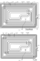
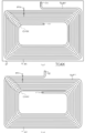
- FIG. 2 is a plan view (I) showing the structure of the coil of the second embodiment, (a) is the plan view (i), and (b) is the plan view (ii).
- 2 is a plan view (II) showing the structure of the coil of the second embodiment, (a) is the plan view (iii), and (b) is the plan view (iv).
- It is a circuit diagram which shows the outline structure of the power receiving coil included in the power transmission system of 3rd Embodiment.
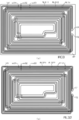
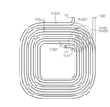
- 3A is a plan view (I) showing the structure of the coil of the third embodiment, (a) is the plan view (i), and (b) is the plan view (ii).
- 3A is a plan view (II) showing the structure of the coil of the third embodiment, (a) is the plan view (iii), and (b) is the plan view (iv).
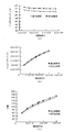
- It is a top view (v) which shows the structure of the coil of 3rd Embodiment. It is a figure which shows the relationship between the capacitance and the transmission efficiency as an effect by the structure of the power receiving coil of 3rd Embodiment.
- FIG. 1 It is a figure which shows the relationship between the capacitance and loss (copper loss) as an effect by the structure of the power receiving coil of 3rd Embodiment.
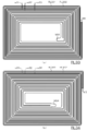
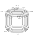
- 4 is a plan view showing the structure of the coil of the conventional example, (a) is the plan view (i), and (b) is the plan view (ii). It is a top view (iii) which shows the structure of the coil of the 4th conventional example.
- FIG. 1 It is a top view (iii) which shows the structure of the coil of the 5th conventional example. It is a figure which shows the effect by the structure of the coil of 5th Embodiment, (a) is a figure which shows the relationship between frequency and inductance as the effect, and (b) is the relationship between frequency and impedance as the effect. (C) is a diagram showing the relationship between the frequency and the Q value as the effect.
- each embodiment described below is a power transmission system in which electric power for charging a storage battery mounted on an electric vehicle is transmitted to an electric vehicle equipped with the storage battery in a non-contact manner by a magnetic field resonance method.
- the electric power transmission system based on the magnetic field resonance method of each embodiment is arranged so as to face (that is, face each other) the power transmission coil described later, which is separated from the power transmission coil, and is sent from the power transmission coil. It is equipped with a power receiving coil, which will be described later, to receive the generated power.
- FIG. 1 is a block diagram showing an outline configuration of the power transmission system of the first embodiment.
- the power transmission system S of the first embodiment includes a power receiving device R including a power receiving unit RV and the power receiving coil RC1, a power transmission device T including a power transmission unit TR and the power transmission coil TC1. It is composed of.
- the power receiving device R is mounted on the electric vehicle and is connected to a storage battery (not shown) mounted on the electric vehicle.
- the power transmission device T is installed on the ground where the electric vehicle moves or stops. Then, when charging the storage battery, the electric vehicle is operated or stopped so that the power receiving coil RC1 of the power receiving device R and the power transmission coil TC1 of the power transmission device T face each other.
- the power transmission device When charging the storage battery by the power transmission system S of the first embodiment, the power transmission device installed on the ground below the stop position of the power receiving device R mounted on the stopped electric vehicle. It can be configured to transmit electric power from the power transmission device T via the power transmission coil TC1 of T.
- the power transmission coil TC1 of a plurality of power transmission devices T installed in a certain distance section of the road on which the electric vehicle is moving is used. Therefore, it may be configured to continuously transmit electric power from the power transmission device T.
- the power transmission unit TR corresponds to an example of the "output means" of the present invention
- the power receiving unit RV corresponds to an example of the "input means" of the present invention.
- the electric power to be transmitted is input to the power transmission coil TC1 from the power transmission unit TR.
- the power receiving coil RC1 outputs the electric power received from the power transmission coil TC1 to the power receiving unit RV by the magnetic field resonance method.
- the power transmission coil TC1 or the power reception coil RC1 correspond to an example of the "coil" of the present invention, respectively.
- the power transmission unit TR of the power transmission device T outputs the power to be transmitted to the power reception device R to the power transmission coil TC1 while complying with the regulations such as the Radio Law in the country where the power transmission system S is used. ..
- the above-mentioned regulations and the like regulate the leakage magnetic field so as to be below a predetermined level in consideration of the influence on the human body, for example.
- the frequency or frequency band in the predetermined range must follow the recommendations of international organizations such as ISO (International Organization for Standardization) or IEC (International Electrotechnical Commission) as the above regulations. Further, since the lower limit value of the transmission efficiency considering the predetermined positional deviation between the power transmission coil TC1 and the power reception coil RC1 is also defined by the above-mentioned international organization, high power transmission efficiency is required for the power transmission system S as well. ..
- the power receiving coil RC1 of the power receiving device R that receives the power from the power transmission coil TC1 by the magnetic field resonance method outputs the received power to the power receiving unit RV.
- the power receiving unit RV converts the output corresponding to the electric power (for example, the high frequency power of 85 kilohertz) into a DC (direct current) current by a power conversion unit (not shown) and outputs the output to the storage battery of the electric vehicle. ..
- the storage battery is charged with a required amount of electric power.
- FIG. 1 (II) Configuration of power transmission coil TC1 (power receiving coil RC1)
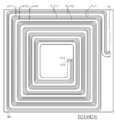
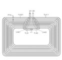
- FIG. 2 to 4 are plan views showing the structure of the power transmission coil TC1 of the first embodiment, and are a plan view of the power transmission device T when the power transmission coil TC is viewed from the power transmission unit TR side (see FIG. 1). Is.
- the power transmission coil TC1 of the first embodiment includes a power transmission loop coil TL11 composed of two parallel copper thin film wires TL111 and a copper thin film wire TL112, and FIG.
- a power transmission loop coil TL12 (not shown) is laminated in a direction perpendicular to the paper surface of FIG. 2 via an insulating film BF (details will be described later).
- the power transmission loop coil TL11 corresponds to an example of the "Volume 1 line" of the present invention
- the power transmission loop coil TL12 corresponds to an example of the "Volume 2 line" of the present invention.
- the copper thin film wire TL111 and the copper thin film wire TL112 correspond to an example of the "first parallel winding line" of the present invention.
- the film BF is used for the insulation between the power transmission loop coil TL11 and the power transmission loop coil TL12, but in addition to these, an insulating material such as a glass epoxy material may be used. can.
- an insulating material such as a glass epoxy material may be used.
- a thin film material in which ceramic particles and the like are dispersed can be used.
- an appropriate void-retaining material may be used so as to be laminated through the required voids.
- the winding center of the copper thin film wire TL111 and the copper thin film wire TL112 constituting the power transmission loop coil TL11 and the winding center of the copper thin film wire described later constituting the power transmission loop coil TL12 are the same or the same as each other. It is almost the same.
- the power transmission loop coil TL11 is a copper thin film wire TL111 and a copper thin film wire wound in parallel with each other in the same layer of the power transmission coil TC1 (the surface of the film BF exemplified in FIG. 2). It is composed of TL112, and has an external connection terminal O1 connected to the copper thin film wire TL111 and the copper thin film wire TL112 and connected to the power transmission unit TR on one side of the outermost peripheral portion thereof.
- the power transmission loop coil TL11 is configured by winding the copper thin film wire TL111 and the copper thin film wire TL112 six times (6 turns) in parallel in the counterclockwise direction from the outermost peripheral portion thereof in FIG.
- each of the copper thin film wire TL111 and the copper thin film wire TL112 are connected to the external connection terminal O1. Further, the inner peripheral ends of each of the copper thin film wire TL111 and the copper thin film wire TL112 (in the case shown in FIG. 2, the central end portion of the transmission coil TC1) are formed by the vias V11 and via V12 penetrating the film BF to form the copper thin film wires. Each of the TL111 and the copper thin film wire TL112 is connected to the copper thin film wire constituting the transmission loop coil TL12 formed on the back surface of the film BF.
- the copper thin film wire TL111 has the same width w11 (see FIG.
- the copper thin film wire TL112 also has the same width w12 (see FIG. 2) and the same thickness over the entire circumference of the power transmission loop coil TL11. Therefore, the width w10 (see FIG. 2) of each winding as the power transmission loop coil TL11 is also the same over the entire circumference of the power transmission loop coil TL11. Then, in the power transmission loop coil TL11, the width w12 of the copper thin film wire TL112 on the inner peripheral side in one winding is wider than the width w11 of the copper thin film wire TL111 on the outer peripheral side in the one winding over the entire circumference. It has been widened.
- each straight line portion is provided on each of the upper side portion, the lower side portion, the left side portion and the right side portion in FIG. 2, and each straight line portion is a curve having a substantially concentric arc shape. It is connected by a part.
- FIG. 3 is a plan view showing only the power transmission loop coil TL12 taken out.
- the power transmission loop coil TL12 laminated on the power transmission loop coil TL11 with the film BF in between is composed of two parallel, for example, copper thin film wires TL121 and copper thin film wires TL122.
- the copper thin film wire TL121 and the copper thin film wire TL122 correspond to an example of the "second parallel winding line" of the present invention.
- the center of the is the same as or substantially the same as each other.
- the overall shape of the power transmission loop coil TL12 is substantially square, which is the same as the overall shape of the power transmission loop coil TL11.
- the power transmission loop coil TL12 is the copper thin film wire TL121 and the copper thin film wire TL121 wound in parallel with each other in the same layer of the power transmission coil TC1 (the back surface of the film BF exemplified in FIG. 2). It is composed of a thin film wire TL122, and has an external connection terminal O2 connected to the copper thin film wire TL121 and the copper thin film wire TL122 and connected to the power transmission unit TR on one side of the outermost peripheral portion thereof.
- the power transmission loop coil TL12 is configured by winding the copper thin film wire TL121 and the copper thin film wire TL122 six times (6 turns) in parallel in the counterclockwise direction from the innermost peripheral portion of each in FIG.
- each of the copper thin film wire TL121 and the copper thin film wire TL122 are connected to the external connection terminal O2.
- the inner peripheral end of the copper thin film wire TL121 (in the case shown in FIG. 3, the central end of the power transmission coil TC1) is connected to the copper thin film wire TL111 of the power transmission loop coil TL11 by the via V12, and the copper thin film is also formed.
- the inner peripheral end of the wire TL122 is connected to the copper thin film wire TL112 of the power transmission loop coil TL11 by the via V11.
- the copper thin film wire TL121 has the same width w11 and the same thickness over the entire circumference of the power transmission loop coil TL12.
- the copper thin film wire TL122 also has the same width w12 and the same thickness over the entire circumference of the power transmission loop coil TL12. Therefore, the width w10 (see FIG. 3) of each winding of the power transmission loop coil TL12 is also the same over the entire circumference of the power transmission loop coil TL12. Then, in the power transmission loop coil TL12, the width w12 of the copper thin film wire TL122 on the inner peripheral side in one winding is wider than the width w11 of the copper thin film wire TL121 on the outer peripheral side in the one winding over the entire circumference. It has been widened. Further, in each of the copper thin film wire TL121 and the copper thin film wire TL122, a straight line portion is provided on each of the upper side portion, the lower side portion, the left side portion and the right side portion in FIG. It is connected by a part.
- FIG. 4 is a plan view showing the overlapping state of the power transmission loop coil TL11 and the power transmission loop coil TL12.
- the power transmission loop coil TL11 is shown by a solid line, and a film BF (not shown in FIG. 4) is provided directly below the power transmission loop coil TL11.
- the power transmission loop coils TL12 stacked via the wires are shown by broken lines.
- FIG. 4 it is composed of a copper thin film wire TL111 and a copper thin film wire TL112 wound in parallel from the outer circumference to the inner circumference, and at the innermost peripheral portion thereof, by via V11 and via V12.
- a solid line in FIG. 4 it is composed of a copper thin film wire TL111 and a copper thin film wire TL112 wound in parallel from the outer circumference to the inner circumference, and at the innermost peripheral portion thereof, by via V11 and via V12.
- the transmission loop coil TL11 connected to the copper thin film wire TL121 and the copper thin film wire TL122 constituting the transmission loop coil TL12, one of the four curved portions included in the one winding portion (for example, FIG. 4).
- each winding of the copper thin film wire TL111 and the copper thin film wire TL112 that is, each winding of the copper thin film wire TL111 and the copper thin film wire TL112 adjacent to each other on each side.
- the radial distance of the power transmission coil TC1 in the above. See FIG. 4).
- the copper thin film wire TL111 and the copper thin film wire TL112 are wound counterclockwise.
- the curved portion whose winding transitions to the inner peripheral side of one pitch PT1 is, for example, six curved portions CV11 arranged from the outer peripheral side to the inner peripheral side in the lower right corner portion in FIG. There will be.
- the copper thin film wire TL111 and the copper thin film wire TL112 constituting the transmission loop coil TL11, and the copper thin film wire TL121 and the copper thin film wire TL122 connected by the via V11 and the via V12 at the innermost peripheral portions thereof are connected from the inner circumference, respectively.
- the transmission loop coil TL12 which is wound in parallel toward the outer periphery, as shown by a broken line in FIG. 4, one of the four curved portions included in the one winding is curved (for example, FIG.
- the position of the straight portion is shifted to the outer peripheral side by one pitch PT1 in each winding of the copper thin film wire TL121 and the copper thin film wire TL122 (that is, the winding is on the outer peripheral side).
- the copper thin film wire TL121 and the copper thin film wire TL122 are wound counterclockwise (that is, in the same direction as the transmission loop coil TL11).
- the curved portions whose windings transition to the outer peripheral side by one pitch PT are, for example, six curved portions CV12 arranged from the inner peripheral side to the outer peripheral side in the lower right corner portion in FIG. It will be.
- the outermost peripheral portion of the power transmission loop coil TL11 on the right side in FIG. 4 is connected to the external connection terminal O1 having a shape protruding outward, and the outermost peripheral portion of the power transmission loop coil TL12 on the right side in FIG. 4 protrudes outward.
- the shape is such that it is connected to the external connection terminal O2.
- the positions of are the same except for the curved portion where each winding transitions and the connection portion to the external connection terminal O1 and the external connection terminal O2.
- the position of the copper thin film wire TL112 and the position of the copper thin film wire TL122 as viewed from the center of the power transmission coil TC1 are also the curved portion where each winding transitions and the connection portion to the external connection terminal O1 and the external connection terminal O2. It is the same except for.
- the power transmission loop coil TL11 and the power transmission loop coil TL12 sandwich the film BF in a state where at least each straight portion of the power transmission loop coil TL11 and at least each straight part of the power transmission loop coil TL12 overlap. It is laminated with.
- the power transmission loop is formed at the innermost peripheral portion of the power transmission loop coil TL11 so as to have the same winding direction with respect to the counterclockwise winding from the outermost peripheral portion (external connection terminal O1) to the innermost peripheral portion.
- the coil TL12 is connected, and the power transmission loop coil TL12 is wound from the innermost peripheral portion to the outermost peripheral portion while maintaining the winding direction.
- a current flows counterclockwise from the outermost peripheral portion to the innermost peripheral portion in the power transmission loop coil TL11, and the current flows in the innermost part in the power transmission loop coil TL12. It flows in the same counterclockwise direction from the peripheral part to the outermost part.
- the manufacturing method is basically the same as the conventional first manufacturing method including the following steps (a) -1 to (a) -6, or the following (b) -1 to (b) -12.
- a second manufacturing method or the like including each step of the above can be used.
- (a) First manufacturing method (a) -1: A copper thin film is formed on the entire both sides of the film BF (a) -2: A resist is placed on each of the copper thin films (both sides) formed in the above (a) -1.
- the width and thickness of each of the copper thin film wire TL111 and the copper thin film wire TL112 are the transmission loop coil TL11. It is the same from the outermost outermost end portion (connection portion to the external connection terminal O1 (external connection terminal O2)) of the (transmission loop coil TL12) to the innermost peripheral end portion where the via V11 and the via V12 are connected.
- Patterning (b) -6 Copper thin film wire TL121 and copper thin film wire TL122) are subjected to etching treatment after patterning of the above (b) -5, and external connection terminal O1 (external connection terminal O2), copper thin film wire TL111 and copper thin film are subjected to etching treatment.
- Forming wire TL112 copper thin film wire TL121 and copper thin film wire TL122
- (b) -7 External connection terminal O1 and external connection terminal O2 and transmission unit TR (in the case of power transmission device T) or power reception unit RV (power receiving device R) If) and connect
- the power transmission frequency of the power transmission system S using the power transmission coil TC1 or the power reception coil RC1 of the first embodiment having the configurations shown in FIGS. 2 to 4 is changed to change the power transmission frequency of the power transmission coil TC1 or the power reception coil RC1.
- the results of measuring the impedance will be described with reference to FIGS. 5 to 8 as the first embodiment in comparison with the power transmission coil (power receiving coil) of the first conventional example.
- 5 to 7 are plan views showing the structure of the coil of the first conventional example, respectively, and FIG. 8 shows the frequency and impedance as effects of the structure of the power transmission coil TC1 or the power receiving coil RC1 of the first embodiment. It is a figure which shows the relationship.
- FIGS. 5 to 7 are plan views showing the structure of the power transmission coil of the first conventional example when viewed from the same viewpoint as the power transmission coil TC1 of the first embodiment (see FIG. 1).
- the same members as those of the power transmission coil TC1 of the first embodiment are designated by the same member numbers, and detailed description thereof will be omitted.
- the power transmission coil TCX of the first conventional example includes a power transmission loop coil TLX composed of two parallel copper thin film wires TLX1 and a copper thin film wire TLX2, and is shown in FIG.
- the power transmission loop coil TLY which is not used, is laminated in the direction perpendicular to the paper surface of FIG. 5 via an insulating film BF similar to the power transmission coil TC1 of the first embodiment.
- the center of winding of the copper thin film wire TLX1 and the copper thin film wire TLX2 constituting the power transmission loop coil TLX and the center of winding of the copper thin film wire constituting the power transmission loop coil TLY will be the same or the same as each other. It is almost the same.
- the power transmission loop coil TLX is a copper thin film wire TLX1 and a copper thin film wire wound in parallel with each other in the same layer of the power transmission coil TCX (the surface of the film BF exemplified in FIG. 5). It is composed of TLX2, and has an external connection terminal O1 for connecting the copper thin film wire TLX1 and the copper thin film wire TLX2 on one side of the outermost peripheral portion thereof.
- the transmission loop coil TLX is configured by winding the copper thin film wire TLX1 and the copper thin film wire TLX2 six times (6 turns) in parallel in the counterclockwise direction from the outermost peripheral portion thereof in FIG.
- the outer peripheral end portions center of the right side portion in the case of FIG.
- each of the copper thin film wire TLX1 and the copper thin film wire TLX2 are connected to the external connection terminal O1. Further, the inner peripheral ends of the copper thin film wires TLX1 and the copper thin film wires TLX2 (in the case shown in FIG. 5, the central end of the transmission coil TCX) are formed by the vias V11 and via V12 penetrating the film BF to form the copper thin film wires. Each of the TLX1 and the copper thin film wire TLX2 is connected to the copper thin film wire constituting the transmission loop coil TLY formed on the back surface of the film BF.
- the copper thin film wire TLX1 has the same width w11 (see FIGS.
- the copper thin film wire TLX2 also has the same width w12 (see FIGS. 2 and 5) and the same thickness over the entire circumference of the power transmission loop coil TLX. Therefore, the width w10 of each winding as the power transmission loop coil TLX (see FIGS. 2 and 5) is also the same over the entire circumference of the power transmission loop coil TLX. In the power transmission loop coil TLX, the width w12 of the copper thin film wire TLX2 on the inner peripheral side in one winding is wider than the width w11 of the copper thin film wire TLX1 on the outer peripheral side in one winding over the entire circumference. Has been done.
- each straight line portion is provided on each of the upper side portion, the lower side portion, the left side portion and the right side portion in FIG. 5, and each straight line portion is a curve having a substantially concentric arc shape. It is connected by a part.
- FIG. 6 is a plan view showing only the power transmission loop coil TLY taken out.
- the power transmission loop coil TLY laminated on the power transmission loop coil TLX with the film BF in between is composed of two parallel copper thin film wires TLY1 and copper thin film wires TLY2. ing.
- the center of winding of the copper thin film wire TLY1 and the copper thin film wire TLY2 constituting the power transmission loop coil TLY and the winding center of the copper thin film wire TLX1 and the copper thin film wire TLX2 constituting the power transmission loop coil TLX are , Mutually identical or substantially identical.
- the overall shape of the power transmission loop coil TLY is substantially square, which is the same as the overall shape of the power transmission loop coil TLX.
- the power transmission loop coil TLY is the copper thin film wire TLY1 and the copper thin film wire TLY1 wound in parallel with each other in the same layer of the power transmission coil TCX (the back surface of the film BF exemplified in FIG. 5). It is composed of a thin film wire TLY2, and has an external connection terminal O2 for connecting the copper thin film wire TLY1 and the copper thin film wire TLY2 on one side of the outermost peripheral portion thereof.
- the power transmission loop coil TLY is configured by winding the copper thin film wire TLY1 and the copper thin film wire TLY2 six times (6 turns) in parallel in the counterclockwise direction from the innermost peripheral portion of each in FIG.
- the outer peripheral end portions center of the right side portion in the case of FIG.
- each of the copper thin film wire TLY1 and the copper thin film wire TLY2 are connected to the external connection terminal O2.
- the inner peripheral end portion of the copper thin film wire TLY1 (in the case shown in FIG. 6, the central end portion of the power transmission coil TCY) is connected to the copper thin film wire TLX1 of the power transmission loop coil TLX by the via V12, and the copper thin film is also formed.
- the inner peripheral end of the wire TLY2 is connected to the copper thin film wire TLX2 of the power transmission loop coil TLX by the via V11.
- the copper thin film wire TLY1 has the same width w11 and the same thickness over the entire circumference of the power transmission loop coil TLY.
- the copper thin film wire TLY2 also has the same width w12 and the same thickness over the entire circumference of the power transmission loop coil TLY. Therefore, the width w10 (see FIG. 6) of each winding as the power transmission loop coil TLY is also the same over the entire circumference of the power transmission loop coil TLY.
- the width w12 of the copper thin film wire TLY2 on the inner peripheral side in one winding is wider than the width w11 of the copper thin film wire TLY1 on the outer peripheral side in one winding over the entire circumference.
- a straight line portion is provided on each of the upper side portion, the lower side portion, the left side portion, and the right side portion in FIG. It is connected by a part.
- FIG. 7 is a plan view showing the overlapping state of the power transmission loop coil TLX and the power transmission loop coil TLY.
- the power transmission loop coil TLX is shown by a solid line, and a film BF (not shown in FIG. 7) is directly below the power transmission loop coil TLX.
- the power transmission loop coils TLY stacked via each are shown by broken lines.
- a solid line in FIG. 7 it is composed of a copper thin film wire TLX1 and a copper thin film wire TLX2 wound in parallel from the outer circumference to the inner circumference, and at the innermost peripheral portion thereof, by via V11 and via V12.
- the position of the straight line portion is inside by one quarter of the pitch PT1 for each quarter of the circumference.
- Each curved portion is formed so as to shift to the circumferential side (that is, the winding shifts to the inner peripheral side), and the copper thin film wire TLX1 and the copper thin film wire TLX2 are wound counterclockwise.
- the copper thin film wire TLX1 and the copper thin film wire TLX2 constituting the transmission loop coil TLX and the copper thin film wire TLY1 and the copper thin film wire TLY2 connected by the via V11 and the via V12 at the innermost peripheral portions thereof are connected from the inner circumference, respectively.
- the transmission loop coil TLY which is wound in parallel toward the outer circumference, as shown by the broken line in FIG. 7, the position of the straight line portion of the pitch PT1 is set by one quarter of the pitch PT1 for each quarter of the circumference.
- Each curved portion is formed so as to shift to the outer peripheral side (that is, the winding shifts to the outer peripheral side), and the copper thin film wire TLY1 and the copper thin film wire TLY2 are counterclockwise (that is, in the same direction as the transmission loop coil TLX). It is wound around. Then, the outermost peripheral portion on the right side in FIG. 7 of the power transmission loop coil TLX is connected to the external connection terminal O1 having a shape protruding outward, and the outermost peripheral portion on the right side in FIG. 7 of the power transmission loop coil TLY protrudes outward.
- the shape is such that it is connected to the external connection terminal O2.
- the position of the copper thin film wire TLX1 and the copper thin film wire TLY1 as seen from the center of the power transmission coil TCX are different as shown in FIG.
- the positions of the copper thin film wire TLX2 and the copper thin film wire TLY2 as seen from the center of the power transmission coil TCX are also different as shown in FIG. 7. Therefore, as the power transmission coil TCX, the power transmission loop coil TLX and the power transmission loop coil TLY are laminated so as to sandwich the film BF in a state where the power transmission loop coil TLX and the power transmission loop coil TLY do not overlap.
- the power transmission loop is formed at the innermost peripheral portion of the power transmission loop coil TLX so that the winding direction is the same as the counterclockwise winding from the outermost peripheral portion (external connection terminal O1) to the innermost peripheral portion.
- the coil TLY is connected, and the power transmission loop coil TLY is wound from the innermost peripheral portion to the outermost peripheral portion while maintaining the winding direction. Due to this structure, as the power transmission coil TCX of the first conventional example, a current flows counterclockwise from the outermost peripheral portion to the innermost peripheral portion in the power transmission loop coil TLX, and the current flows in the innermost part in the power transmission loop coil TLY. It flows in the same counterclockwise direction from the peripheral part to the outermost part.
- the other specifications of the power transmission coil TC1 of the first embodiment and the power transmission coil TCX of the first conventional example used in the experiment of the first embodiment are as follows. In the following description, the specifications of the power transmission coil TC1 and the power transmission coil TCX will be described, but the specifications of the power reception coil RC1 of the first embodiment used in the experiment are the same as the specifications of the power transmission coil TC1. The specifications of the power receiving coil of the first conventional example are the same as the specifications of the power transmission coil TCX.
- the impedance is about 2/3 lower than that when the power transmission coil TCX and the power reception coil are used.
- the impedance is preferably less than 0.5 ohm when the power transmission is performed at a frequency of 85 kilohertz. Even in light of this, it can be said that a configuration such as the transmission coil TC1 and the power receiving coil RC1 (that is, a configuration in which the copper thin film wires constituting each overlap) is more preferable for the reduction of impedance.
- the power transmission coil TC1 (power receiving coil RC1) has a plurality of straight lines.
- a power transmission loop coil TL11 (outer circumference ⁇ inner circumference winding) and a power transmission loop coil TL12 (inner circumference ⁇ outer circumference winding) made of a copper thin film wire TL111 or the like having a portion and a plurality of curved portions are laminated with the film BF interposed therebetween. It has a different configuration.
- the power transmission loop coil TL11 and the power transmission loop coil TL12 each have substantially square shapes (may be polygons other than squares) having the same overall shape in plan view, and the power transmission coil TC1 (power receiving) of each winding of the power transmission loop coil TL11.
- the position seen from the center of the coil RC1) and the position seen from the center of the power transmission coil TC1 (power receiving coil RC1) of each winding of the power transmission loop coil TL12 coincide with each other in a plan view (see FIG. 4).
- the winding transition for one winding is performed only in one curved portion (CV11 (see FIG. 4)) included in one winding, and the power transmission loop coil is also wound.
- the power transmission coil TC1 and the corresponding thin film conductor transmission coil TC1 and The positions of the power receiving coil RC1 as viewed from the center can be reliably aligned with each other in a plan view.
- the transmission loop coil TL11 is composed of the copper thin film wire TL111 and the copper thin film wire TL112
- the transmission loop coil TL12 is composed of the copper thin film wire TL121 and the copper thin film wire TL122, the impedance can be further reduced. By being able to do so, it is possible to further achieve both weight reduction and cost reduction, improvement of transmission efficiency, and prevention of an increase in operating temperature.
- the width w12 of the copper thin film wire TL112 (copper thin film wire TL122) on the inner peripheral side is wider than the width w11 of the copper thin film wire TL111 (copper thin film wire TL121) on the outer peripheral side, the impedance can be further reduced. This makes it possible to achieve both weight reduction and cost reduction, improvement of transmission efficiency, and prevention of an increase in operating temperature.
- FIGS. 9 and 10 are plan views showing the structure of the coil of the second embodiment, respectively.
- the case where it is configured has been described (see FIGS. 2 to 4).
- the first power transmission loop coil made of a copper thin film wire wound from the outer peripheral side to the inner peripheral side and the inner peripheral side thereof.
- the second power transmission loop coil which is a second power transmission loop coil made of a copper thin film wire wound around the outer peripheral side and is connected in series to the first power transmission loop coil, is a power transmission coil (and power reception). It is formed so as to fit in one layer of the coil), and two such layers are further laminated to form a power transmission coil (and a power reception coil).
- a coil for current adjustment hereinafter, "current adjustment coil" is connected in series with the first power transmission loop coil and the second power transmission loop coil. Is called) is connected.
- the configurations of the power transmission coil of the second embodiment and the power reception coil of the second embodiment are basically the same, and the power reception loop coil of the power reception coil of the second embodiment and the power transmission coil of the second embodiment have the same configuration.
- the configuration of each power transmission loop coil is the same.
- the configurations of the current adjusting coil in the power transmission coil of the second embodiment and the current adjusting coil in the power receiving coil of the second embodiment are also the same. Therefore, in the following description, the configuration of the power transmission coil of the second embodiment will be described only. At this time, the same constituent members as those of the power transmission coil TC1 of the first embodiment are designated by the same member numbers, and detailed description thereof will be omitted.
- the power transmission coil TC2 of the second embodiment is a power transmission loop coil TL21 composed of two parallel copper thin film wires TL211 and a copper thin film wire TL212.
- the first power transmission loop coil and the second power transmission loop coil (corresponding to the second power transmission loop coil) and the power transmission loop coil TL22 whose plan view is shown in FIG. It is configured by stacking in the direction perpendicular to the paper surface.
- the center of winding of the copper thin film wire TL211 and the copper thin film wire TL212 constituting the power transmission loop coil TL21, and the copper thin film wire TL221 and the copper thin film wire TL222 constituting the power transmission loop coil TL22 (see FIG. 9B).
- the center of winding is the same as or substantially the same as each other.
- the transmission loop coil TL21 is a copper thin film wound in the same layer of the transmission coil TC2 (the surface of the film BF exemplified in FIG. 9A) in parallel with each other. It is composed of a wire TL211 and a copper thin film wire TL212, and the copper thin film wire TL211 and the copper thin film wire TL212 are connected to one side of the outermost periphery thereof (center of the right side in the case shown in FIG. 9A) and power is transmitted.
- An external connection terminal O1 for connecting to the unit TR, and a connection terminal M1 and a connection terminal M2 for separately connecting the copper thin film wire TL211 and the copper thin film wire TL212 to the current adjusting coil of the second embodiment described later, respectively. have.
- the copper thin film wire TL211 and the copper thin film wire TL212 are arranged in parallel in the counterclockwise direction from the external connection terminal O1 at the outermost periphery thereof to the innermost peripheral portion thereof in FIG. 9A. It is wound half a turn (2.5 turns), and further, it is wound two and a half turns (2.5 turns) in parallel in the counterclockwise direction from the innermost peripheral portion to the connection terminal M1 and the connection terminal M2. It is configured.
- each of the copper thin film wire TL211 and the copper thin film wire TL212 is provided with a straight line portion on each of the upper side portion, the lower side portion, the left side portion and the right side portion in FIG. They are connected by concentric arcuate curved portions.
- the width w21 of the copper thin film wire TL211 is wider toward the inner peripheral side of the power transmission coil TC2.
- the width w21 is the same in each straight portion constituting the copper thin film wire TL211. In each curved portion connecting the straight portions, the width w21 is changed (that is, wider toward the inner peripheral side of the power transmission coil TC2). (Changed to be).
- the thickness of the copper thin film wire TL211 is the same over the entire circumference of the power transmission loop coil TL21.
- the width w22 of the copper thin film wire TL212 is also wider toward the inner peripheral side of the power transmission coil TC2, similarly to the width w21.
- This width w22 is the same in each straight portion constituting the copper thin film wire TL212, and the width w22 is changed (that is, wider toward the inner peripheral side of the power transmission coil TC2) in each curved portion connecting the straight portions. (Changed to be).
- the thickness of the copper thin film wire TL212 is the same over the entire circumference of the power transmission loop coil TL21. With the above configuration, the width w20 of each winding as the power transmission loop coil TL21 (see FIG. 9A) is also wider toward the inner peripheral side of the power transmission coil TC2.
- the width w22 of the copper thin film wire TL212 on the inner peripheral side in one turn is wider than the width w21 of the copper thin film wire TL211 on the outer peripheral side in the one turn. It has been widened.
- FIG. 9B is a plan view showing only the power transmission loop coil TL22 taken out.
- the overall shape of the power transmission loop coil TL22 is substantially rectangular, which is the same as the overall shape of the power transmission loop coil TL21.
- the transmission loop coil TL22 laminated on the transmission loop coil TL21 with the film BF in between is in the same layer of the transmission coil TC2 (FIG. 9A). It is composed of a copper thin film wire TL221 and a copper thin film wire TL222 wound in parallel with each other (the back surface of the illustrated film BF), and one side of the outermost peripheral portion thereof (the right side in the case of FIG. 9B).
- An external connection terminal O1 for connecting the copper thin film wire TL221 and the copper thin film wire TL222 and connecting to the transmission unit TR in parallel with the transmission loop coil TL21, and the copper thin film wire TL221 and the copper thin film wire TL222 are connected to the center).
- connection terminal M1 and a connection terminal M2 for separately connecting to the current adjusting coil of the second embodiment.
- the external connection terminal O1, the connection terminal M1 and the connection terminal M2 are the same as the external connection terminal O1 and the connection terminal M1 and the connection terminal M2 shown in FIG. 9A.
- the copper thin film wire TL221 and the copper thin film wire TL222 are two in parallel in the counterclockwise direction from the external connection terminal O1 at the outermost periphery thereof to the innermost peripheral portion thereof in FIG. 9B.
- each of the copper thin film wire TL221 and the copper thin film wire TL222 a straight line portion is provided on each of the upper side portion, the lower side portion, the left side portion and the right side portion in FIG. They are connected by concentric arcuate curved portions.
- the width w21 of the copper thin film wire TL221 is the same as the width w21 of the copper thin film wire TL211 shown in FIG. 9A, and is wider toward the inner peripheral side of the power transmission coil TC2.
- the width w21 is the same in each straight portion constituting the copper thin film wire TL221, and the width w21 is changed (that is, wider toward the inner peripheral side of the power transmission coil TC2) in each curved portion connecting the straight portions. (Changed to be).
- the thickness of the copper thin film wire TL221 is the same over the entire circumference of the power transmission loop coil TL22.
- the width w22 of the copper thin film wire TL222 is the same as the width w22 of the copper thin film wire TL212 of the power transmission loop coil TL21 shown in FIG. 9A, and is the same as the width w21 of the copper thin film wire TL221. It is wider toward the inner circumference of.
- This width w22 is the same in each straight portion constituting the copper thin film wire TL222, and the width w22 is changed (that is, wider toward the inner peripheral side of the power transmission coil TC2) in each curved portion connecting the straight portions. (Changed to be).
- the thickness of the copper thin film wire TL222 is the same over the entire circumference of the power transmission loop coil TL21.
- the width w20 of each winding as the power transmission loop coil TL22 is also the inner circumference of the power transmission coil TC2. It is wider toward the side.
- the width w22 of the copper thin film wire TL222 on the inner peripheral side in one winding is wider than the width w21 of the copper thin film wire TL221 on the outer peripheral side in the one winding over the entire circumference. It has been widened.
- FIG. 10A is a plan view showing only the current adjusting coil taken out. Further, the overall shape of the current adjusting coil is substantially rectangular, which is the same as the overall shape of each of the power transmission loop coil TL21 and the power transmission loop coil TL22.
- the current adjusting coil TL23 laminated with the film sandwiched directly under the transmission loop coil TL22 is wound in the same layer of the transmission coil TC2 in parallel with each other. It is composed of a copper thin film wire TL231 and a copper thin film wire TL232, and the outermost peripheral end thereof is a copper thin film wire TL231 and a copper thin film wire TL232, the copper thin film wire TL211 and the copper thin film wire TL212, and the copper thin film wire TL212.
- the connection terminal M1 and the connection terminal M2 for separately connecting to the TL221 and the copper thin film wire TL222, respectively.
- connection terminal M1 and the connection terminal M2 are the same as the connection terminal M1 and the connection terminal M2 shown in FIG. 9, respectively.
- the innermost peripheral end of the copper thin film wire TL231 and the copper thin film wire TL232 is an external connection terminal O2 for connecting the copper thin film wire TL231 and the copper thin film wire TL232 and connecting to the power transmission unit TR.
- the external connection terminal O2 penetrates the film between the current adjusting coil TL23 and the power transmission loop coil TL22 and the film BF between the power transmission loop coil TL22 and the power transmission loop coil TL21, and is external as shown in FIG. 9A. It is configured to be exposed on the same surface as the connection terminal O1.
- the copper thin film wire TL231 and the copper thin film wire TL232 are shown in FIG. 10A from the connection terminal M1 and the connection terminal M2 at the outermost periphery thereof to the external connection terminal O2 at the innermost periphery thereof. It is configured to be wound five times (5 turns) in parallel in the counterclockwise direction. As a result, the total number of turns (five rotations) of the power transmission loop coil TL21 and the power transmission loop coil TL22 is an integral multiple (one times) of the number of turns of the current adjustment coil TL23.
- each of the copper thin film wire TL231 and the copper thin film wire TL232 a straight line portion is provided on each of the upper side portion, the lower side portion, the left side portion and the right side portion in FIG. They are connected by concentric arcuate curved portions. Further, the center of winding of the copper thin film wire TL211 and the copper thin film wire TL212, the winding center of the copper thin film wire TL221 and the copper thin film wire TL222, and the winding of the copper thin film wire TL231 and the copper thin film wire TL232. The centers are the same or substantially the same as each other.
- the width w21 of the copper thin film wire TL231 is the width w21 of the copper thin film wire TL211 of the power transmission loop coil TL21 shown in FIG. 9A and the width w21 of the copper thin film wire TL221 of the power transmission loop coil TL22 shown in FIG. 9B. It is the same as the above, and is wider toward the inner peripheral side of the power transmission coil TC2.
- the width w21 is the same in each straight portion constituting the copper thin film wire TL231, and the width w21 is changed (that is, wider toward the inner peripheral side of the power transmission coil TC2) in each curved portion connecting the straight portions. (Changed to be).
- the thickness of the copper thin film wire TL231 is the same over the entire circumference of the current adjusting coil TL23.
- the width w22 of the copper thin film wire TL232 is the same as the width w22 of the copper thin film wire TL212 shown in FIG. 9A and the width w22 of the copper thin film wire TL222 shown in FIG. 9B, and the copper thin film wire TL231. Similar to the width w21 of, the width is wider toward the inner peripheral side of the transmission coil TC2.
- the width w23 is the same in each straight portion constituting the copper thin film wire TL232, and the width w22 is changed (that is, wider toward the inner peripheral side of the power transmission coil TC2) in each curved portion connecting the straight portions. (Changed to be).
- the thickness of the copper thin film wire TL232 is the same over the entire circumference of the current adjusting coil TL23.
- the width w22 of the copper thin film wire TL232 on the inner peripheral side in one winding is wider than the width w21 of the copper thin film wire TL231 on the outer peripheral side in the one winding over the entire circumference. It has been widened.
- FIG. 10B is a plan view showing the overlapping state of the transmission loop coil TL21, the transmission loop coil TL22 and the current adjustment coil TL23, and the transmission loop coil TL21 is shown by a solid line and the film BF is directly below the transmission loop coil TL21 (FIG. 10B). ),
- the transmission loop coil TL22 laminated via the transmission loop coil TL22 is shown by a broken line, and the current adjusting coil TL23 laminated via the film directly under the transmission loop coil TL22 is shown by a dotted chain line. ing.
- the four curved portions included in the one winding Only in one curved portion for example, the curved portion in the lower right corner portion in FIG. 10 (b)
- one pitch PT2 in each winding of the copper thin film wire TL211 and the copper thin film wire TL212 see FIG. 10 (b)
- the copper thin film wire TL211 and the copper thin film wire TL212 are connected to the external connection terminal O1 so that the position of the straight portion is shifted toward the outer peripheral side or the inner peripheral side (that is, the winding is transferred to the outer peripheral side or the inner peripheral side).
- the curved portion whose winding transitions to the outer peripheral side or the inner peripheral side by one pitch PT 2 minutes is included in, for example, the four curved portions in the lower right corner portion in FIG. 10B. It will be.
- the copper thin film wire TL211 and the copper thin film wire TL212 and the copper thin film wire TL221 and the copper thin film wire TL221 and the copper thin film wire TL221 and the copper thin film wire TL212 and the copper thin film wire TL212 and the copper thin film wire TL212 and the copper thin film wire TL212 and the copper thin film wire TL212 and the copper thin film wire TL212 which are connected to each other at the outermost periphery thereof by the external connection terminal O1 and the connection terminal M1 and the connection terminal M2, which constitute the transmission loop coil TL21, respectively.
- the transmission loop coil TL22 composed of the wire TL222, as shown by a broken line in FIG. 10B, in one of the four curved portions included in the winding, one of the curved portions (for example, in FIG.
- the position of the straight part is shifted to the outer peripheral side or the inner peripheral side by one pitch PT2 in each winding of the copper thin film wire TL221 and the copper thin film wire TL222 (that is, the winding is the outer circumference).
- the copper thin film wire TL221 and the copper thin film wire TL222 are wound counterclockwise (that is, in the same direction as the transmission loop coil TL21) so as to transition to the side or the inner peripheral side.
- the curved portion whose winding transitions to the outer peripheral side or the inner peripheral side by one pitch PT 2 minutes is included in, for example, the four curved portions in the lower right corner portion in FIG.
- the copper thin film wire TL211 and the copper thin film wire TL212, and the copper thin film wire TL231 and the copper thin film wire TL232 connected to the copper thin film wire TL221 and the copper thin film wire TL222 via the connection terminal M1 and the connection terminal M2 are from the outer circumference to the inner circumference.
- the current adjusting coil TL23 which is wound in parallel toward the above direction, as shown by a one-point chain line in FIG. 10B, one of the four curved portions included in the one winding portion (one of the curved portions ( For example, only in the curved portion of the lower right corner portion in FIG.
- the position of the straight portion is shifted to the inner peripheral side by one pitch PT2 in each winding of the copper thin film wire TL231 and the copper thin film wire TL232 ( That is, the copper thin film wire TL231 and the copper thin film wire TL232 are wound counterclockwise (that is, in the same direction as the transmission loop coil TL21 and the transmission loop coil TL22) so that the winding shifts to the inner peripheral side).
- the curved portion whose winding transitions to the inner peripheral side of one pitch PT2 is, for example, four curves arranged from the outer peripheral side to the inner peripheral side in the lower right corner portion in FIG. 10B. It will be a group.
- the outermost peripheral end of the current adjusting coil TL23 is the connection terminal M1 and the connection terminal M2, and the innermost peripheral end thereof is the external connection terminal O2.
- the power transmission loop coil TL21, the power transmission loop coil TL22, and the current adjustment coil TL23 having the above shapes are laminated as shown in FIG. 10B, so that the copper thin film wire seen from the center of the power transmission coil TC2. TL211 It is the same.
- the positions of the copper thin film wire TL212, the copper thin film wire TL222, and the copper thin film wire TL232 as viewed from the center of the power transmission coil TC2 are also the curved portions where the respective windings transition, and the external connection terminal O1 and the external connection terminal O2. It is the same except for the connection portion to the connection terminal M1 and the connection terminal M2.
- the power transmission coil TC2 at least each straight part of the power transmission loop coil TL21, at least each straight part of the power transmission loop coil TL22, and at least each straight part of the current adjustment coil TL23 are overlapped with each other.
- the TL21 to the current adjusting coil TL23 are laminated with the film BF and the like interposed therebetween.
- the outermost peripheral portion of the transmission loop coil TL21 and the outermost peripheral portion of the transmission loop coil TL22 (external connection terminal O1) ⁇ their innermost peripheral portions ⁇ the connection terminals M1 and the connection terminals M2 of their outermost peripheral portions are in this order.
- the copper thin film wire TL211 and the copper thin film wire TL212, the copper thin film wire TL221 and the copper thin film wire TL222 are wound counterclockwise. Then, the copper thin film wire TL231 and the copper thin film wire TL232 of the current adjusting coil TL23 are wound counterclockwise from the connection terminal M1 and the connection terminal M2 to the innermost peripheral portion thereof, and the innermost peripheral end portion thereof is the external connection terminal O2. It is connected to the.
- a current flows counterclockwise from the external connection terminal O1 to the connection terminal M1 and the connection terminal M2 in the power transmission loop coil TL21 and the power transmission loop coil TL22, and then the connection terminal.
- the current flows from M1 and the connection terminal M2 to the external connection terminal O2 in the current adjustment coil TL23 in the same counterclockwise direction.
- the manufacturing method of the power transmission coil TC2 and the power receiving coil RC2 of the second embodiment is basically the same as the manufacturing method of the power transmission coil TC1 and the power receiving coil RC1 of the first embodiment. Omit.
- the second conventional example to be compared with the second embodiment is the power transmission loop coil TL21 and the power transmission loop coil TL22 in the power transmission coil TC2 or the power reception coil RC2 of the second embodiment.
- the number of turns of the current adjusting coil TL23 is eight, and the other structures such as the number of turns of the current adjusting coil TL23 are the same as those of the power transmission coil TC2 or the power receiving coil RC2 of the second embodiment.
- the number of turns (8 rotations) of each power transmission loop coil included therein is an integral multiple of the number of turns (5 rotations) of the current adjustment coil RL23. Therefore, the positions of the copper thin film wires constituting the power transmission loop coil and the like and the current adjusting coil RL23 do not overlap each other when viewed from the center thereof.
- the other specifications of the power transmission coil TC2 of the second embodiment and the power transmission coil of the second conventional example used in the experiment of the second embodiment are as follows. In the following description, the specifications of the power transmission coil TC2 and the power transmission coil of the second conventional example will be described, but the specifications of the power reception coil RC2 of the second embodiment used in the experiment are the specifications of the power transmission coil TC2. It is the same, and the specifications of the power receiving coil of the second conventional example are the same as the specifications of the power transmission coil of the second conventional example.
- Distance between power transmission coil and power receiving coil 40 mm ⁇ Ferrite sheet with the same thickness as power transmission coil and power receiving coil, respectively, It is provided on the surface opposite to the facing surface of each coil.
- the power using the power transmission system S of the first embodiment is the width w21 and width w22 of the copper thin film wire TL211 and the copper thin film wire TL212, the copper thin film wire TL221 and the copper thin film wire TL222, and the copper thin film wire TL231 and the copper thin film wire TL232, respectively, are the power transmission coil TC2 and the like.
- the width of the copper thin film wire is wider toward the center of the power transmission coil TC2 or the like where the current is concentrated, so that the impedance of the power transmission coil TC2 or the like can be further reduced. can.
- FIGS. 11 to 16 are circuit diagram showing an outline configuration of a power receiving coil included in the power transmission system of the third embodiment
- FIGS. 12 to 14 are plan views showing the structure of the coil of the third embodiment
- FIG. 15 is a diagram showing the relationship between the capacitance as an effect due to the configuration of the power receiving coil of the third embodiment and the transmission efficiency
- FIG. 16 is a diagram showing the capacitance as an effect due to the structure of the power receiving coil of the third embodiment. It is a figure which shows the relationship with loss (copper loss).
- the power transmission coil TC1 (power receiving coil RC1) of the first embodiment described above, the case where the power transmission coil TC1 is composed of the two power transmission loop coil TL11 and the power transmission loop coil TL12 has been described (see FIGS. 2 to 4).
- the power receiving coil of the third embodiment described below includes the first power receiving loop coil having the same configuration as the power transmission loop coil TL21 of the second embodiment and the power transmission loop coil TL22 of the second embodiment.
- a second power receiving loop coil having the same configuration as the above, and a coil for current adjustment (hereinafter referred to as "current adjustment coil") independent of the first power receiving loop coil and the second power receiving loop coil are used. It is configured to be laminated.
- the power receiving coil of the third embodiment will be mainly described, but the power receiving coil of the third embodiment and the power transmission coil of the third embodiment may have the same configuration. Further, in the following description, the same component numbers as those of the power receiving coil RC1 (that is, the power transmission coil TC1) of the first embodiment are designated by the same member numbers, and detailed description thereof will be omitted.
- the power receiving coil RC3 of the third embodiment includes an external connection terminal O1 and an external connection terminal O2, two power receiving loop coils RL31 and a power receiving loop coil RL32, and two current adjusting coils RL33 and current adjusting. It is configured to include a coil RL34 and a capacitor Cp for adjusting a current.
- the current adjusting capacitor is simply referred to as a "current adjusting capacitor”.
- the current adjusting capacitor Cp corresponds to an example of the "capacitive means" of the present invention.
- the external connection terminal O1 and the external connection terminal O2 are external connection terminals for connecting the power receiving coil RC3 to the power receiving unit RV, respectively.
- the power receiving loop coil RL31 and the power receiving loop coil RL32 are connected in series to the external connection terminal O1 and the external connection terminal O2, and are connected to each other in parallel.
- the current adjusting coil RL33 and the current adjusting coil RL34 are insulated from the power receiving loop coil RL31 and the power receiving loop coil RL32, and are connected to each other in series by the connection terminal M3.
- the current adjusting capacitor Cp is connected to both ends of the current adjusting coil RL33 and the current adjusting coil RL34.
- the current adjusting capacitor Cp, the current adjusting coil RL33, the current adjusting coil having the same configuration as the current adjusting coil RL34, and the two current adjusting coils form the third embodiment of the power transmission system together with the power receiving coil RC3. It may be provided in the transmission coil of the embodiment.
- the current adjusting capacitor Cp, the current adjusting coil RL33, and the current adjusting coil RL34 mainly contribute to the reduction of impedance and the improvement of transmission efficiency.
- the power receiving loop coil RL31 of the third embodiment described below (corresponding to the first power receiving loop coil described above) is basically the same as the power transmission loop coil TL21 of the second embodiment except for the number of turns. It has a configuration.
- the power receiving loop coil RL32 of the third embodiment (corresponding to the second power receiving loop coil described above) has basically the same configuration as the power transmission loop coil TL22 of the second embodiment except for the number of turns thereof. ing.
- the power receiving coil RC3 of the third embodiment includes a power receiving loop coil RL31 composed of two parallel copper thin film wires RL311 and a copper thin film wire RL312.
- the power receiving loop coil RL32 whose plan view is shown in FIG. 12B is laminated via an insulating film BF in a direction perpendicular to the paper surface of FIG.
- the winding center of the copper thin film wire RL311 and the copper thin film wire RL312 and the winding center of the copper thin film wire RL321 and the copper thin film wire RL322 are the same or substantially the same as each other. Has been done.
- the power receiving loop coil RL31 is a copper thin film wound in the same layer of the power receiving coil RC3 (the surface of the film BF exemplified in FIG. 12 (a)) in parallel with each other. It is composed of wire RL311 and copper thin film wire RL312, and the copper thin film wire RL311 and the copper thin film wire RL312 are connected to one side of the outermost periphery thereof (center of the right side in the case shown in FIG. 12A) and power is transmitted. It has an external connection terminal O1 and an external connection terminal O2 for connecting to the unit TR.
- the copper thin film wire RL311 and the copper thin film wire RL312 are arranged in parallel in the counterclockwise direction from the external connection terminal O1 on the outermost peripheral portion thereof to the innermost peripheral portion thereof in FIG. 12 (a). It is rotated (4 turns) and further rotated 4 times (4 turns) in parallel in the counterclockwise direction from the innermost peripheral portion to the external connection terminal O2. Further, for the intersecting portion in the winding of the copper thin film wire RL311 and the copper thin film wire RL312, a laminated structure in which an insulating layer is sandwiched and the copper thin film wire RL311 and the copper thin film wire RL312 are conducted by a via VV, or a jumper wire is used.
- each of the copper thin film wire RL311 and the copper thin film wire RL312 a straight line portion is provided on each of the upper side portion, the lower side portion, the left side portion, and the right side portion in FIG. They are connected by concentric arcuate curved portions.
- the width w31 of the copper thin film wire RL311 is wider toward the inner peripheral side of the power receiving coil RC3.
- the width w31 is the same in each straight portion constituting the copper thin film wire RL311, and the width w31 is changed (that is, wider toward the inner peripheral side of the power receiving coil RC3) in each curved portion connecting the straight portions.
- the thickness of the copper thin film wire RL311 is the same over the entire circumference of the power receiving loop coil RL31.
- the width w32 of the copper thin film wire RL312 is also wider toward the inner peripheral side of the power receiving coil RC3, similarly to the width w31.
- the width w32 is the same in each straight portion constituting the copper thin film wire RL312, and the width w32 is changed (that is, wider toward the inner peripheral side of the power receiving coil RC3) in each curved portion connecting the straight portions. (Changed to be).
- the thickness of the copper thin film wire RL312 is the same over the entire circumference of the power receiving loop coil RL31.
- the width w30 of each winding as the power receiving loop coil RL31 is also wider toward the inner peripheral side of the power receiving coil RC3. Then, in the power receiving loop coil RL31, the width w32 of the copper thin film wire RL312 on the inner peripheral side in one winding is wider than the width w31 of the copper thin film wire RL311 on the outer peripheral side in the one winding over the entire circumference. It has been widened.
- FIG. 12B is a plan view showing only the power receiving loop coil RL32 taken out.
- the overall shape of the power receiving loop coil RL32 is substantially rectangular, which is the same as the overall shape of the power receiving loop coil RL31.
- the power receiving loop coil RL32 laminated on the power receiving loop coil RL31 with the film BF in between is in the same layer of the power receiving coil RC3 (FIG. 12A). It is composed of a copper thin film wire RL321 and a copper thin film wire RL322 wound in parallel with each other (the back surface of the illustrated film BF), and one side of the outermost peripheral portion thereof (the right side in the case of FIG. 12B).
- the center of the section) has an external connection terminal O1 and an external connection terminal O2 for connecting the copper thin film wire RL321 and the copper thin film wire RL322 and connecting to the power transmission section TR in parallel with the power receiving loop coil RL31.
- the external connection terminal O1 and the external connection terminal O2 are the same as the external connection terminal O1 and the external connection terminal O2 shown in FIG. 12 (a).
- the copper thin film wire RL321 and the copper thin film wire RL322 are arranged in parallel in the counterclockwise direction from the external connection terminal O1 on the outermost peripheral portion thereof to the innermost peripheral portion thereof in FIG. 12 (b). It is rotated (4 turns) and further rotated 4 times (4 turns) in parallel in the counterclockwise direction from the innermost peripheral portion to the external connection terminal O2.
- a laminated structure in which an insulating layer is sandwiched and the copper thin film wire RL321 and the copper thin film wire RL322 are conducted by a via VV, or a jumper wire is used. They are crossed at seven points (see FIG. 12B) while being insulated from each other by a method or the like. Further, in each of the copper thin film wire RL321 and the copper thin film wire RL322, a straight line portion is provided on each of the upper side portion, the lower side portion, the left side portion and the right side portion in FIG. They are connected by concentric arcuate curved portions.
- the width w31 of the copper thin film wire RL321 is the same as the width w31 of the copper thin film wire RL311, and is wider toward the inner peripheral side of the power receiving coil RC3.
- the width w31 is the same in each straight portion constituting the copper thin film wire RL321, and the width w31 is changed (that is, wider toward the inner peripheral side of the power receiving coil RC3) in each curved portion connecting the straight portions. (Changed to be).
- the thickness of the copper thin film wire RL321 is the same over the entire circumference of the power receiving loop coil RL32.
- the width w32 of the copper thin film wire RL322 is the same as the width w32 of the copper thin film wire RL312, and is wider toward the inner peripheral side of the power receiving coil RC3 as in the width w31.
- the width w32 is the same in each straight portion constituting the copper thin film wire RL322, and the width w32 is changed (that is, wider toward the inner peripheral side of the power receiving coil RC3) in each curved portion connecting the straight portions. (Changed to be).
- the thickness of the copper thin film wire RL322 is the same over the entire circumference of the power receiving loop coil RL32. With the above configuration, the width w30 of each winding as the power receiving loop coil RL32 (see FIG.
- the width w32 of the copper thin film wire RL322 on the inner peripheral side in one winding is wider than the width w31 of the copper thin film wire RL321 on the outer peripheral side in the one winding over the entire circumference. It has been widened.
- FIG. 13A is a plan view showing only the current adjusting coil RL33 taken out.
- the overall shape of the current adjusting coil RL33 and the current adjusting coil RL34 described later is substantially rectangular, which is the same as the overall shape of each of the power receiving loop coil RL31 and the power receiving loop coil RL32.
- the current adjusting coil RL33 laminated with the film sandwiched directly under the power receiving loop coil RL32 is wound in the same layer of the power receiving coil RC3 in parallel with each other.
- the copper thin film wire RL331 and the copper thin film wire RL332 are configured, and the outermost peripheral end thereof is a current adjusting coil RL34 for which the copper thin film wire RL331 and the copper thin film wire RL332 are described with reference to FIG. 13 (b). It is a connection terminal M3 for separately connecting in series to the copper thin film wire RL341 and the copper thin film wire RL342.
- the copper thin film wire RL331 to the copper thin film wire RL342 correspond to an example of the "adjusting winding line" of the present invention.
- the innermost peripheral end of the copper thin film wire RL331 and the copper thin film wire RL332 is a connection terminal M33 for connecting the copper thin film wire RL331 and the copper thin film wire RL332 and connecting the current adjusting capacitor Cp.
- the copper thin film wire RL331 and the copper thin film wire RL332 are parallel in the clockwise direction from the connection terminal M3 at the outermost periphery thereof to the connection terminal M33 at the innermost periphery thereof in FIG. 13A. It is composed of eight turns (8 turns).
- each of the copper thin film wire RL331 and the copper thin film wire RL332 a straight line portion is provided on each of the upper side portion, the lower side portion, the left side portion, and the right side portion in FIG. They are connected by concentric arcuate curved portions.
- the center of the winding of the copper thin film wire RL311 and the copper thin film wire RL312, the center of the winding of the copper thin film wire RL321 and the copper thin film wire RL322, and the center of the winding of the copper thin film wire RL331 and the copper thin film wire RL332. Are the same or substantially the same as each other.
- the width w31 of the copper thin film wire RL331 is the same as the width w31 of the copper thin film wire RL311 and the width w31 of the copper thin film wire RL321, and is wider toward the inner peripheral side of the power receiving coil RC3.
- the width w31 is the same in each straight portion constituting the copper thin film wire RL331, and the width w31 is changed (that is, wider toward the inner peripheral side of the power receiving coil RC3) in each curved portion connecting the straight portions. (Changed to be).
- the thickness of the copper thin film wire RL331 is the same over the entire circumference of the current adjusting coil RL33.
- the width w32 of the copper thin film wire RL332 is the width w32 of the copper thin film wire RL312 of the power receiving loop coil RL31 shown in FIG. 12 (a) and the width of the copper thin film wire RL322 of the power receiving loop coil RL32 shown in FIG. It is the same as w32, and is wider toward the inner peripheral side of the power receiving coil RC3, like the width w31 of the copper thin film wire RL331.
- the width w32 is the same in each straight portion constituting the copper thin film wire RL332, and the width w32 is changed (that is, wider toward the inner peripheral side of the power receiving coil RC3) in each curved portion connecting the straight portions. (Changed to be).
- the thickness of the copper thin film wire RL332 is the same over the entire circumference of the current adjusting coil RL33.
- the width w30 of each winding as the current adjusting coil RL33 (the same as the width w30 in the power receiving loop coil RL31 shown in FIG. 12A and the width w30 in the power receiving loop coil RL32 shown in FIG. 12B). 13 (a)) is also wider toward the inner peripheral side of the power receiving coil RC3.
- the width w32 of the copper thin film wire RL332 on the inner peripheral side in one winding is wider than the width w31 of the copper thin film wire RL331 on the outer peripheral side in the one winding over the entire circumference. It has been widened.
- FIG. 13B is a plan view showing only the current adjusting coil RL34 taken out.
- the current adjusting coil RL34 laminated with the film sandwiched directly under the current adjusting coil RL33 is wound in the same layer of the power receiving coil RC3 in parallel with each other. It is composed of a copper thin film wire RL341 and a copper thin film wire RL342, and the outermost peripheral end thereof is a copper thin film wire RL341 and a copper thin film wire RL342. It is said that the connection terminal M3 is used to connect the two separately in series. At this time, the connection terminal M3 is the same as the connection terminal M3 shown in FIG. 13 (a).
- the innermost peripheral end of the copper thin film wire RL341 and the copper thin film wire RL342 is a connection terminal M34 for connecting the copper thin film wire RL341 and the copper thin film wire RL342 and connecting the current adjusting capacitor Cp.
- the copper thin film wire RL341 and the copper thin film wire RL342 are parallel in the clockwise direction from the connection terminal M34 at the innermost peripheral portion thereof to the connection terminal M3 at the outermost peripheral portion thereof in FIG. 13B. It is composed of eight turns (8 turns).
- each of the copper thin film wire RL341 and the copper thin film wire RL342 a straight line portion is provided on each of the upper side portion, the lower side portion, the left side portion, and the right side portion in FIG. They are connected by concentric arcuate curved portions.
- the winding centers of the copper thin film wire RL341 and the copper thin film wire RL342 are the same or substantially the same as each other.
- the width w31 of the copper thin film wire RL341 is the same as the width w31 of the copper thin film wire RL311, the width w31 of the copper thin film wire RL321, and the width w31 of the copper thin film wire RL331. It's getting wider.
- the width w31 is the same in each straight portion constituting the copper thin film wire RL341, and the width w31 is changed (that is, wider toward the inner peripheral side of the power receiving coil RC3) in each curved portion connecting the straight portions. (Changed to be).
- the thickness of the copper thin film wire RL341 is the same over the entire circumference of the current adjusting coil RL34.
- the width w32 of the copper thin film wire RL342 is the same as the width w32 of the copper thin film wire RL312, the width w32 of the copper thin film wire RL322, and the width w32 of the copper thin film wire RL332, and the width of the copper thin film wire RL341. Similar to w31, it is wider toward the inner peripheral side of the power receiving coil RC3.
- the width w32 is the same in each straight portion constituting the copper thin film wire RL342, and the width w32 is changed (that is, wider toward the inner peripheral side of the power receiving coil RC3) in each curved portion connecting the straight portions. (Changed to be).
- the thickness of the copper thin film wire RL342 is the same over the entire circumference of the current adjusting coil RL34.
- the width w30 of each winding as the current adjusting coil RL34 width w30 in the power receiving loop coil RL31 shown in FIG. 12A, width w30 in the power receiving loop coil RL32 shown in FIG. 12B, and FIG. 13 ( It is the same as the width w30 in the current adjusting coil RL33 shown in a). See FIG. 13B), which is also wider toward the inner peripheral side of the power receiving coil RC3.
- the width w32 of the copper thin film wire RL342 on the inner peripheral side in one winding is wider than the width w31 of the copper thin film wire RL341 on the outer peripheral side in the one winding over the entire circumference. It has been widened.
- (Six rotations) is an integral multiple (double) of the (electrical) number of turns (eight rotations) of the combined power receiving loop coil TL31 and the power receiving loop coil TL32 connected in parallel.
- FIG. 14 is a plan view showing the overlapping state of the power receiving loop coil RL31, the power receiving loop coil RL32, the current adjusting coil RL33 and the current adjusting coil RL34.
- the power receiving loop coil RL32 laminated via the power receiving loop coil RL32 is shown by a broken line, and the current adjusting coil RL33 laminated via the film is connected directly below the power receiving loop coil RL32 by a single point chain wire.
- the current adjusting coil RL34 laminated directly under the RL33 via a film is shown by a two-point chain wire.
- one of the four curved portions included in the one winding Only in the curved portion (for example, the curved portion in the lower right corner portion in FIG. 14), one pitch PT3 (see FIGS. 12 (b) and 14) in each winding of the copper thin film wire RL311 and the copper thin film wire RL312 is a straight line thereof.
- the copper thin film wire RL311 and the copper thin film wire RL312 are externally connected from the external connection terminal O1 so that the position of the portion shifts to the outer peripheral side or the inner peripheral side (that is, the winding shifts to the outer peripheral side or the inner peripheral side). It is wound counterclockwise to the terminal O2.
- the curved portion whose winding transitions to the outer peripheral side or the inner peripheral side of one pitch PT3 minutes is included in, for example, the seven curved portions in the lower right corner portion in FIG. ..
- the copper thin film wire RL321 and the copper thin film wire RL322 are wound counterclockwise (that is, in the same direction as the power receiving loop coil RL31).
- the curved portion whose winding transitions to the outer peripheral side or the inner peripheral side of one pitch PT3 minutes is included in, for example, the four curved portions in the lower right corner portion in FIG. ..
- the outermost peripheral ends of the power receiving loop coil RL31 and the power receiving loop coil RL32 on the right side of FIG. 14 are connected to the external connection terminal O1 and the external connection terminal O2, respectively.
- the copper thin film wire RL33 is included in the one winding as shown by the one-point chain line in FIG. Only in one of the four curved portions (for example, the curved portion in the lower right corner portion in FIG. 14), one pitch PT3 in each winding of the copper thin film wire RL331 and the copper thin film wire RL332 of the straight portion thereof.
- the copper thin film wire RL331 and the copper thin film wire RL332 are wound clockwise so that the position shifts to the inner peripheral side (that is, the winding shifts to the inner peripheral side).
- the curved portion whose winding transitions to the inner peripheral side of one pitch PT3 is, for example, seven curved portions arranged from the outer peripheral side to the inner peripheral side in the lower right corner portion in FIG. There will be.
- the outermost peripheral end of the current adjusting coil RL33 is the connection terminal M3, and the innermost peripheral end thereof is the connection terminal M33.
- the curved portions whose windings transition to the outer peripheral side of one pitch PT 3 minutes are, for example, seven curved portions arranged from the outer peripheral side to the inner peripheral side in the lower right corner portion in FIG. It will be.
- the innermost peripheral end of the current adjusting coil RL34 is the connection terminal M34, and the outermost peripheral end thereof is the connection terminal M3.
- the power receiving loop coil RL31, the power receiving loop coil RL32, the current adjusting coil RL33, and the current adjusting coil RL34 having the above shapes are laminated as shown in FIG.
- the positions of the thin film wire RL311, the copper thin film wire RL321, the copper thin film wire RL331, and the copper thin film wire RL341 are the curved portion where each winding transitions, the external connection terminal O1 and the external connection terminal O2, the connection terminal M3, and the connection terminal M33. It is the same except for the connection portion to the connection terminal M34.
- the positions of the copper thin film wire RL312, the copper thin film wire RL322, the copper thin film wire RL332, and the copper thin film wire RL342 viewed from the center of the power receiving coil RC3 are also the curved portions where the windings change and the external connection terminal O1. It is the same except for the connection portion to the external connection terminal O2, the connection terminal M3, the connection terminal M33, and the connection terminal M34. Therefore, as the power receiving coil RC3, at least each straight portion of the power receiving loop coil RL31, at least each straight portion of the power receiving loop coil RL32, at least each straight portion of the current adjusting coil RL33, and at least each straight portion of the current adjusting coil RL34.
- the power receiving loop coil RL31 to the current adjusting coil RL34 are laminated with the film BF and the like interposed therebetween.
- the outermost peripheral portion of the power receiving loop coil RL31 and the outermost peripheral portion of the power receiving loop coil RL32 (external connection terminal O1) ⁇ their innermost peripheral portions ⁇ the external connection terminal O2 of their outermost peripheral portions are counterclockwise.
- the copper thin film wire RL311, the copper thin film wire RL312, the copper thin film wire RL321, and the copper thin film wire RL322 are wound in the direction.
- the copper thin film wire RL341 and the copper thin film wire RL342 of the current adjusting coil RL34 are wound clockwise from the connection terminal M34 to the connection terminal M3 at the outermost periphery thereof, and further, the current adjusting coil is clockwise from the connection terminal M3.
- the copper thin film wire RL331 and the copper thin film wire RL332 of the RL33 are wound up to the connection terminal M33 at the innermost peripheral portion thereof, and the current adjustment capacitor Cp is connected to the connection terminal M33 and the connection terminal M34.
- the optimum value of the capacity of the current adjusting capacitor Cp will be described later as a third embodiment.
- a current flows between the external connection terminal O1 and the external connection terminal O2 in the power receiving loop coil RL31 and the power receiving loop coil RL32, and the current value is the current adjusting coil. It is adjusted by the RL33, the current adjustment coil RL34, and the current adjustment capacitor Cp.
- the manufacturing method of the power transmission coil and the power receiving coil RC3 of the third embodiment is basically the same as the manufacturing method of the power transmission coil TC1 and the power receiving coil RC1 of the first embodiment, detailed description thereof will be omitted. do.
- the horizontal axis shows the capacity of the current adjustment capacitor Cp
- the vertical axis shows the loss (copper loss) in each of the current adjustment coil RL33 (current adjustment coil RL34) and the power receiving loop coil RL31 (power receiving loop coil RL32). Is shown.
- the power receiving coil RC3 of the third embodiment is different from the current adjusting coil RL33 and the current adjusting coil RL34.
- This part has the same configuration as the power receiving coil RC2 (power transmission coil TC2) of the second embodiment.
- the total number of turns (16 rotations) of the current adjusting coil RL33 and the current adjusting coil RL34 connected in series is the same as that of the transmission loop coil and the power receiving loop coil connected in parallel. It is not an integral multiple of the number of turns (ten turns), and therefore the positions of the copper thin film wires constituting the power receiving loop coil and the like and the current adjusting coil do not overlap when viewed from the center.
- the other specifications of the power receiving coil RC3 of the third embodiment and the power receiving coil of the third conventional example used in the experiment of the third embodiment are as follows.
- the transmission efficiency is lowered when the capacity of the current adjusting capacitor Cp is 20 microfarads or more.
- the copper loss in the power receiving loop coil RL31 power receiving loop coil RL32
- the capacitance of the current adjusting capacitor Cp at the above frequency is preferably 20 microfarads or less.
- the power transmission system S of the first embodiment and the power of the second embodiment are used.
- the current adjustment coil RL33 and the current adjustment coil RL34 are further provided, and the overall shape in the plan view is the same as the overall shape in the plan view of the power receiving loop coil RL31 and the power receiving loop coil RL32.
- the current adjusting coil RL33 and the current adjusting coil RL34 are laminated at the same positions as the power receiving loop coil RL31 and the power receiving loop coil RL32, the current flowing through the power receiving loop coil RL31 and the power receiving loop coil RL32 can be effectively adjusted. It is possible to achieve both weight reduction and cost reduction, improvement of transmission efficiency, and prevention of an increase in operating temperature.
- the current adjusting coil RL33 and the current adjusting coil RL34 are connected in series at the outermost peripheral end thereof, and the current adjusting capacitor Cp is connected to the innermost peripheral portion thereof, and its capacity is optimal for the frequency of power transmission. (It is said to be 20 microfarads or less), so even if a current adjustment capacitor Cp is provided, it is possible to achieve both weight reduction and cost reduction, improvement of transmission efficiency, and prevention of an increase in operating temperature. can.
- FIGS. 17 and 18 are plan views showing the structure of the coil of the fourth embodiment, respectively.
- the power transmission loop coil is such that the position of the straight line portion in the winding of the power transmission loop coil TL11 shifts to the outer peripheral side or the inner peripheral side (that is, the winding shifts to the outer peripheral side or the inner peripheral side).
- the copper thin film wire TL111 and the copper thin film wire TL112 constituting the TL11 were wound (see, for example, FIG. 4 or FIG. 10B).
- the transmission coil (and the power receiving coil) of the fourth embodiment described below one turn in the transmission loop coil (and the power receiving loop coil) which is laminated with each other to form the transmission coil (and the power receiving coil).
- the position of the straight part shifts to the outer peripheral side or the inner peripheral side by one pitch in the winding of the transmission loop coil (and the power receiving loop coil). (That is, the winding transitions to the outer peripheral side or the inner peripheral side), the copper thin film wire constituting the transmission loop coil (and the power receiving loop coil) is wound.
- the position of each winding of the stacked power transmission loop coils (and power receiving loop coil) as seen from the center of the power transmission coil (power receiving coil) is flat. It is configured so that the matching part in the visual view becomes wider.
- the configurations of the power transmission coil of the fourth embodiment and the power reception coil of the fourth embodiment are basically the same, and the power reception loop coil of the power reception coil of the fourth embodiment and the power transmission coil of the fourth embodiment have the same configuration.
- the configuration of each power transmission loop coil is the same. Therefore, in the following description, the configuration of the power transmission coil of the fourth embodiment will be described only. At this time, the same components as those of the power transmission coil TC1 of the first embodiment are designated by the same member numbers, and detailed description thereof will be omitted.
- the power transmission coil TC4 of the fourth embodiment has a power transmission loop coil TL41 configured by a copper thin film wire TL411 and a plan view thereof in FIG. 17 (b).
- the power transmission loop coil TL42 and the power transmission loop coil TL42 showing the above are laminated in a direction perpendicular to the paper surface of FIG. 17 via an insulating film BF.
- the winding center of the copper thin film wire TL411 constituting the power transmission loop coil TL41 and the winding center of the copper thin film wire TL421 (see FIG. 17B) constituting the power transmission loop coil TL42 are mutually identical. Or they are almost the same.
- the power transmission loop coil TL41 is composed of a copper thin film wire TL411 wound in one layer of the power transmission coil TC4 (the surface of the film BF exemplified in FIG. 17A).
- An external connection terminal O1 for connecting the copper thin film wire TL411 to a power transmission unit (not shown) is provided on one side of the outermost peripheral portion thereof.
- the power transmission loop coil TL41 is configured by winding the copper thin film wire TL411 clockwise six times (6 turns) from the outermost peripheral portion thereof in FIG. 17A, and is configured by winding the copper thin film wire TL411 at the outer peripheral end of the copper thin film wire TL411.
- a portion in the case of FIG.
- the center of the upper side portion is connected to the external connection terminal O1.
- the inner peripheral end portion of the copper thin film wire TL411 (in the case of FIG. 17A, the central end portion of the power transmission coil TC4) is formed on the back surface of the film BF by the via V11 penetrating the film BF. It is connected to a copper thin film wire constituting the power transmission loop coil TL42.
- the copper thin film wire TL411 has the same width and the same thickness over the entire circumference of the power transmission loop coil TL41.
- a straight line portion is provided on each of the upper side portion, the lower side portion, the left side portion and the right side portion in FIG. 17A, and each straight line portion is connected by a substantially concentric arcuate curved portion. ing.
- FIG. 17B is a plan view showing only the power transmission loop coil TL42 taken out.
- the power transmission loop coil TL42 laminated on the power transmission loop coil TL41 with the film BF in between is composed of, for example, a copper thin film wire TL421.
- the center of winding of the copper thin film wire TL421 constituting the power transmission loop coil TL42 and the center of winding of the copper thin film wire TL411 constituting the power transmission loop coil TL41 are the same or abbreviated to each other. It is the same.
- the overall shape of the power transmission loop coil TL42 is substantially rectangular, which is the same as the overall shape of the power transmission loop coil TL41.
- the power transmission loop coil TL42 is a copper thin film wire wound in another layer of the power transmission coil TC4 (the back surface of the film BF exemplified in FIG. 17A). It is composed of TL421, and has an external connection terminal O2 for connecting the copper thin film wire TL421 to the power transmission section (not shown above) on one side of the outermost peripheral portion thereof.
- the power transmission loop coil TL42 is configured by winding the copper thin film wire TL421 clockwise six times (6 turns) from the innermost peripheral portion thereof in FIG. 17B, and is configured by winding the copper thin film wire TL421 at the outer peripheral end of the copper thin film wire TL421. A portion (in the case of FIG.
- the center of the upper side portion is connected to the external connection terminal O2.
- the inner peripheral end portion of the copper thin film wire TL421 (in the case shown in FIG. 17B, the central end portion of the power transmission coil TC4) is connected to the copper thin film wire TL411 of the power transmission loop coil TL41 by the via V11. ..
- the copper thin film wire TL421 has the same width and the same thickness over the entire circumference of the power transmission loop coil TL42.
- a straight line portion is provided on each of the upper side portion, the lower side portion, the left side portion and the right side portion in FIG. 17B, and each straight line portion is connected by a substantially concentric arcuate curved portion. ing.
- FIG. 18 is a plan view showing the overlapping state of the power transmission loop coil TL41 and the power transmission loop coil TL42.
- the power transmission loop coil TL41 (copper thin film wire TL411) is shown as a solid line, and the film BF (shown in FIG. 18) is directly below the power transmission loop coil TL41.
- the power transmission loop coil TL42 (copper thin film wire TL421) laminated via (omitted) is shown by a broken line.
- a solid line in FIG. 18 it is composed of a copper thin film wire TL411 wound from the outer circumference to the inner circumference, and at the innermost peripheral portion thereof, a copper thin film wire TL421 constituting a transmission loop coil TL42 by a via V11.
- a copper thin film wire TL411 wound from the outer circumference to the inner circumference, and at the innermost peripheral portion thereof, a copper thin film wire TL421 constituting a transmission loop coil TL42 by a via V11.
- the straight portion for example, the upper side portion in FIG. 18.
- the copper thin film wire TL411 is rotated clockwise so that the position of the straight line portion of the pitch PT4 (see FIGS. 17 (a) and 18) shifts to the inner peripheral side (that is, the winding shifts to the inner peripheral side). It is wound around.
- the linear portion whose winding transitions to the inner peripheral side of one pitch PT4 is, for example, arranged from the outer peripheral side to the inner peripheral side on the upper side portion in FIGS. 17 (a) and 18; It will be one straight line portion LA41.
- the copper thin film wire TL411 constituting the transmission loop coil TL41 and the copper thin film wire TL421 connected at the innermost peripheral portion thereof by the via V11 are wound from the inner circumference toward the outer circumference.
- only one of the four straight lines included in the winding is the one in the winding of the copper thin film wire TL421.
- the copper thin film wire TL421 rotates clockwise (that is, power transmission) so that the position of the straight line portion shifts to the outer peripheral side (that is, the winding shifts to the outer peripheral side) by pitch PT4 (see FIGS. 17B and 18).
- the linear portions whose windings transition to the outer peripheral side of one pitch PT 4 minutes are, for example, six linear portions arranged from the inner peripheral side to the outer peripheral side on the upper side in FIGS. 17 (b) and 18. It will be the straight line portion LA42.
- the outermost peripheral portion of the uppermost side of the power transmission loop coil TL41 in FIG. 18 is connected to the external connection terminal O1 having a shape protruding outward, and the outermost peripheral portion of the power transmission loop coil TL42 on the right side of FIG. 18 protrudes outward.
- the shape is such that it is connected to the external connection terminal O2.
- the positions of are the same except for the linear portion where each winding transitions and the connection portion to the external connection terminal O1 and the external connection terminal O2. Therefore, as the power transmission coil TC4, each straight part (excluding the winding transition part) and each curved part of the power transmission loop coil TL41, each straight part (excluding the winding transition part) and each of the power transmission loop coil TL42.
- the power transmission loop coil TL41 and the power transmission loop coil TL42 are laminated so as to sandwich the film BF in a state where the curved portions are all overlapped.
- the power transmission loop coil at the innermost peripheral portion of the power transmission loop coil TL41 has the same winding direction as the clockwise winding from the outermost peripheral portion (external connection terminal O1) to the innermost peripheral portion.
- the TL42 is connected, and the power transmission loop coil TL42 is wound from the innermost peripheral portion to the outermost peripheral portion while maintaining the winding direction.
- a current flows clockwise from the outermost peripheral portion to the innermost peripheral portion of the power transmission loop coil TL41, and the current flows to the innermost circumference of the power transmission loop coil TL42. It flows in the same clockwise direction from the part to the outermost part.
- the method of manufacturing the power transmission coil TC4 (and the power receiving coil) of the fourth embodiment is basically the same as the above-mentioned manufacturing method of the power transmission coil TC1 and the power receiving coil RC1 of the first embodiment. Is omitted.
- FIGS. 19 to 21 are plan views showing the structure of the coil of the fourth comparative example
- FIG. 21 is a diagram showing the effect of the structure of the power transmission coil TC4 (or power receiving coil) of the fourth embodiment.
- FIGS. 19 and 20 are plan views showing the structure of the power transmission coil of the fourth comparative example when viewed from the same viewpoint as the power transmission coil TC4 of the fourth embodiment.
- the same members as those of the power transmission coil TC4 of the fourth embodiment are designated by the same member numbers, and detailed description thereof will be omitted.
- the power transmission coil TC4X of the fourth comparative example includes a power transmission loop coil TL4X composed of a copper thin film wire TL4X1 and a power transmission loop coil (not shown in FIG. 19 (a)).
- TL4Y and TL4Y are laminated in a direction perpendicular to the paper surface of FIG. 19 via an insulating film BF similar to the power transmission coil TC4 of the fourth embodiment.
- the center of winding of the copper thin film wire TL4X1 constituting the power transmission loop coil TL4X and the center of winding of the copper thin film wire constituting the power transmission loop coil TL4Y are set to be the same or substantially the same. There is.
- the power transmission loop coil TL4X is composed of a copper thin film wire TL4X1 wound in one layer of the power transmission coil TC4X (the surface of the film BF exemplified in FIG. 19A).
- An external connection terminal O1 for connecting the copper thin film wire TL4X1 to a power transmission unit (not shown) is provided on one side of the outermost peripheral portion thereof.
- the power transmission loop coil TL4X is configured by winding the copper thin film wire TL4X1 six times (6 turns) clockwise from the outermost peripheral portion thereof in FIG. 19 (a), and the outer peripheral end of the copper thin film wire TL4X1.
- a portion in the case of FIG.
- the center of the upper side portion is connected to the external connection terminal O1.
- the inner peripheral end portion of the copper thin film wire TL4X1 (the central end portion of the power transmission coil TC4X in the case shown in FIG. 19A) is formed on the back surface of the film BF by the via V11 penetrating the film BF. It is connected to the copper thin film wire constituting the power transmission loop coil TL4Y.
- the copper thin film wire TL4X1 has the same width and the same thickness over the entire circumference of the power transmission loop coil TL4X.
- a straight line portion is provided on each of the upper side portion, the lower side portion, the left side portion and the right side portion in FIG. 19A, and each straight line portion is connected by a substantially concentric arcuate curved portion. ing.
- FIG. 19B is a plan view showing only the power transmission loop coil TL4Y taken out.
- the power transmission loop coil TL4Y laminated on the power transmission loop coil TL4X with the film BF in between is composed of a copper thin film wire TL4Y1.
- the center of winding of the copper thin film wire TL4Y1 constituting the power transmission loop coil TL4Y and the center of winding of the copper thin film wire TL4X1 constituting the power transmission loop coil TL4X are the same or substantially the same as each other.
- the overall shape of the power transmission loop coil TL4Y is substantially rectangular, which is the same as the overall shape of the power transmission loop coil TL4X.
- the power transmission loop coil TL4Y is a copper thin film wire wound in another layer of the power transmission coil TC4X (the back surface of the film BF exemplified in FIG. 19A). It is composed of TL4Y1 and has an external connection terminal O2 for connecting the copper thin film wire TL4Y1 to a power transmission unit (not shown) on one side of the outermost peripheral portion thereof.
- the power transmission loop coil TL4Y is configured by winding the copper thin film wire TL4Y1 six times (6 turns) clockwise from the innermost peripheral portion thereof in FIG. 19 (b), and the outer peripheral end of the copper thin film wire TL4Y1. A portion (in the case of FIG.
- the center of the upper side portion is connected to the external connection terminal O2.
- the inner peripheral end portion of the copper thin film wire TL4Y1 (the central end portion of the power transmission coil TC4X in the case shown in FIG. 19B) is connected to the copper thin film wire TL4X1 of the power transmission loop coil TL4X by the via V11. ..
- the copper thin film wire TL4Y1 has the same width and the same thickness over the entire circumference of the power transmission loop coil TL4Y.
- a straight line portion is provided on each of the upper side portion, the lower side portion, the left side portion and the right side portion in FIG. 19B, and each straight line portion is connected by a substantially concentric arcuate curved portion. ing.
- FIG. 20 is a plan view showing the overlapping state of the power transmission loop coil TL4X and the power transmission loop coil TL4Y.
- the power transmission loop coil TL4X is shown by a solid line, and a film BF (not shown in FIG. 20) is provided immediately below the solid line.
- the power transmission loop coil TL4Y laminated via the bridge is shown by a broken line.
- a solid line in FIG. 20 it is composed of a copper thin film wire TL4X1 wound from the outer circumference to the inner circumference, and at the innermost peripheral portion thereof, a copper thin film wire TL4Y1 constituting a transmission loop coil TL4Y by a via V11.
- the transmission loop coil TL4X connected to the copper thin film wire TL4X1 only one of the four curved portions included in the winding (for example, the curved portion in the upper left corner portion in FIG. 20) is used.
- the copper thin film wire TL4X1 is wound clockwise so that the position of the straight line portion of each pitch PT4 in the winding shifts to the inner peripheral side (that is, the winding shifts to the inner peripheral side).
- the curved portion whose winding transitions to the inner peripheral side of one pitch PT4 is, for example, arranged from the outer peripheral side to the inner peripheral side at the upper left corner portion in FIGS. 19 (a) and 20. It will be six curved portions CV4X.
- the transmission loop coil TL4Y in which the copper thin film wire TL4X1 constituting the transmission loop coil TL4X and the copper thin film wire TL4Y1 connected at the innermost circumference thereof by the via V11 are wound from the inner circumference toward the outer circumference.
- only one of the four curved portions included in the winding (for example, the curved portion in the upper left corner portion in FIG. 20) is the copper thin film wire TL4Y1.
- the copper thin film wire TL4Y1 is wound clockwise so that the position of the straight line portion of each pitch PT4 in the winding shifts to the outer peripheral side (that is, the winding shifts to the outer peripheral side).
- the curved portion whose winding transitions to the outer peripheral side of one pitch PT4 is, for example, six arranged from the inner peripheral side to the outer peripheral side in the upper left corner portion in FIGS. 19 (b) and 20.
- the outermost peripheral portion of the uppermost side of the power transmission loop coil TL4X in FIG. 20 is connected to the external connection terminal O1 having a shape protruding outward, and the outermost peripheral portion of the uppermost side of the power transmission loop coil TL4Y in FIG. 20 protrudes outward.
- the shape is such that it is connected to the external connection terminal O2.
- the power transmission loop coil TL4X and the power transmission loop coil TL4Y having the above shapes as shown in FIG. 20, the position of the copper thin film wire TL4X1 and the copper thin film wire TL4Y1 as seen from the center of the power transmission coil TC4X. As shown in FIG. 20, the positions of are different in the two curved portions and the connection portions to the external connection terminal O1 and the external connection terminal O2. Therefore, as the power transmission coil TC4X, the power transmission loop coil TL4X and the power transmission loop coil TL4Y are formed in a state where the power transmission loop coil TL4X and the power transmission loop coil TL4Y do not overlap with each other more than the power transmission coil TC4 of the fourth embodiment.
- the power transmission loop coil at the innermost peripheral portion of the power transmission loop coil TL4X has the same winding direction as the clockwise winding from the outermost peripheral portion (external connection terminal O1) to the innermost peripheral portion.
- the TL4Y is connected, and the power transmission loop coil TL4Y is wound from the innermost peripheral portion to the outermost peripheral portion while maintaining the winding direction. Due to this structure, as the power transmission coil TC4X of the fourth comparative example, a current flows clockwise from the outermost peripheral portion to the innermost peripheral portion in the transmission loop coil TL4X, and the current flows in the innermost circumference in the transmission loop coil TL4Y. It flows in the same clockwise direction from the part to the outermost part.
- the other specifications of the power transmission coil TC4 of the fourth embodiment and the power transmission coil TC4X of the fourth comparative example used in the experiment of the fourth embodiment are as follows. In the following description, the specifications of the power transmission coil TC4 and the power transmission coil TC4X will be described, but the specifications of the power reception coil of the fourth embodiment used in the experiment are the same as the specifications of the power transmission coil TC4, and the specifications thereof are the same. 4 The specifications of the power receiving coil of the comparative example are the same as the specifications of the power transmission coil TC4X.
- the transmission coil TC4 and the power receiving coil of the fourth embodiment As shown in FIG. 21, in the vicinity of the frequency (85 kilohertz) used for power transmission by the power transmission system, it is better to use the transmission coil TC4 and the power receiving coil of the fourth embodiment as the transmission coil of the fourth comparative example.
- the impedance is lower than that when the TC4X and the power receiving coil are used, and therefore good characteristics are obtained for the Q value.
- the power transmission loop coil TL41 and the power transmission loop coil TL42 are viewed in plan.
- the overall shape is a substantially rectangular shape that is the same as each other, and the position seen from the center of the power transmission coil TC4 of each winding of the power transmission loop coil TL41 and the position seen from the center of the power transmission coil TC4 of each winding of the power transmission loop coil TL42. And are in agreement in plan view (see FIG. 18).
- FIGS. 22 and 23 are plan views showing the structure of the coil of the fifth embodiment, respectively.
- the copper thin film wire TL111 and the copper thin film wire TL112 constituting the power transmission loop coil TL11 and the copper constituting the power transmission loop coil TL12 are different from the position where The thin film wire TL121 and the copper thin film wire TL122 were wound respectively (see, for example, FIG. 4 or FIG. 10 (b)).
- the transmission coil (and the power receiving coil) of the fifth embodiment described below one turn in the transmission loop coil (and the power receiving loop coil) which is laminated with each other to form the transmission coil (and the power receiving coil).
- the position of the straight part is shifted to the outer peripheral side or the inner peripheral side by one pitch in the winding of the power transmission loop coil (and the power receiving loop coil). (That is, the winding transitions to the outer peripheral side or the inner peripheral side), the copper thin film wire constituting the transmission loop coil (and the power receiving loop coil) is wound.
- the position of one curved portion where the winding transition is performed is set to the same position as viewed from the center of the power transmission coil (and power receiving coil).
- a copper thin film wire constituting the power transmission loop coil (and the power reception loop coil) is wound around the coil.
- each winding of the stacked power transmission loop coils (and power receiving loop coils) has four straight lines and three curves in the one winding.
- the positions of each unit as viewed from the center of the power transmission coil (power receiving coil) are configured to match in a plan view.
- the configurations of the power transmission coil of the fifth embodiment and the power reception coil of the fifth embodiment are basically the same, and the power reception loop coil of the power reception coil of the fifth embodiment and the power transmission coil of the fifth embodiment have the same configuration.
- the configuration of each power transmission loop coil is the same. Therefore, in the following description, the configuration of the power transmission coil according to the fifth embodiment will be described only. At this time, the same components as those of the power transmission coil TC1 of the first embodiment are designated by the same member numbers, and detailed description thereof will be omitted.
- the power transmission coil TC5 of the fifth embodiment has a power transmission loop coil TL51 composed of a copper thin film wire TL511 and a plan view thereof in FIG. 22 (b).
- the power transmission loop coil TL52 and the power transmission loop coil TL52 are laminated in a direction perpendicular to the paper surface of FIG. 22 via an insulating film BF.
- the winding center of the copper thin film wire TL511 constituting the power transmission loop coil TL51 and the winding center of the copper thin film wire TL521 (see FIG. 22B) constituting the power transmission loop coil TL52 are mutually identical. Or they are almost the same.
- the power transmission loop coil TL51 is composed of a copper thin film wire TL511 wound in one layer of the power transmission coil TC5 (the surface of the film BF exemplified in FIG. 22A).
- An external connection terminal O1 for connecting the copper thin film wire TL511 to a power transmission unit (not shown) is provided on one side of the outermost peripheral portion thereof.
- the power transmission loop coil TL51 is configured such that the copper thin film wire TL511 is wound five times (5 turns) counterclockwise from the outermost peripheral portion thereof in FIG. 22A, and the outer circumference of the copper thin film wire T511 is wound.
- the end portion (the right end portion of the upper side portion in the case of FIG. 22A) is connected to the external connection terminal O1.
- the inner peripheral end portion of the copper thin film wire TL511 (in the case of FIG. 22A, the central end portion of the power transmission coil TC5) is formed on the back surface of the film BF by the via V11 penetrating the film BF. It is connected to a copper thin film wire constituting the power transmission loop coil TL52.
- the copper thin film wire TL511 has the same width and the same thickness over the entire circumference of the power transmission loop coil TL51.
- a straight line portion is provided on each of the upper side portion, the lower side portion, the left side portion and the right side portion in FIG. 22A, and each straight line portion is connected by a substantially concentric arcuate curved portion. ing.
- FIG. 22B is a plan view showing only the power transmission loop coil TL52 taken out.
- the power transmission loop coil TL52 laminated on the power transmission loop coil TL51 with the film BF in between is composed of, for example, a copper thin film wire TL521.
- the center of winding of the copper thin film wire TL521 constituting the power transmission loop coil TL52 and the center of winding of the copper thin film wire TL511 constituting the power transmission loop coil TL51 are the same or abbreviated to each other. It is the same.
- the overall shape of the power transmission loop coil TL52 is substantially square, which is the same as the overall shape of the power transmission loop coil TL41.
- the power transmission loop coil TL52 is a copper thin film wire wound in another layer of the power transmission coil TC5 (the back surface of the film BF exemplified in FIG. 22A). It is composed of TL521, and has an external connection terminal O2 for connecting the copper thin film wire TL521 to the power transmission unit (not shown above) on one side of the outermost peripheral portion thereof.
- the power transmission loop coil TL52 is configured by winding the copper thin film wire TL521 counterclockwise five times (5 turns) from the innermost peripheral portion thereof in FIG. 22B, and is configured by winding the copper thin film wire TL521 on the outer circumference of the copper thin film wire TL521.
- the end portion (upper right end portion in the case of FIG.
- the inner peripheral end portion of the copper thin film wire TL521 (the central end portion of the power transmission coil TC5 in the case shown in FIG. 22B) is connected to the copper thin film wire TL511 of the power transmission loop coil TL51 by the via V11. ..
- the copper thin film wire TL521 has the same width and the same thickness over the entire circumference of the power transmission loop coil TL52. Further, in the copper thin film wire TL521, a straight line portion is provided on each of the upper side portion, the lower side portion, the left side portion and the right side portion in FIG. 22B, and each straight line portion is connected by a substantially concentric arcuate curved portion. ing.
- FIG. 23 is a plan view showing the overlapping state of the power transmission loop coil TL51 and the power transmission loop coil TL52.
- the power transmission loop coil TL51 (copper thin film wire TL511) is a solid line, and the film BF (shown in FIG. 23) is directly below the power transmission loop coil TL51.
- the power transmission loop coil TL52 (copper thin film wire TL521) laminated via (omitted) is shown by a broken line.
- the copper thin film wire TL521 is composed of a copper thin film wire TL511 wound from the outer circumference to the inner circumference, and at the innermost peripheral portion thereof, a via V11 constitutes a transmission loop coil TL52.
- a via V11 constitutes a transmission loop coil TL52.
- only one of the four curved portions included in the one winding portion (for example, the upper right portion in FIG. 23) is one of the windings of the copper thin film wire TL511.
- the copper thin film wire TL511 is counterclockwise so that the position of the straight line portion of the pitch PT5 (see FIGS. 22A and 23) shifts to the inner peripheral side (that is, the winding shifts to the inner peripheral side). It is wound around.
- the linear portions whose windings transition to the inner peripheral side of one pitch PT 5 minutes are arranged from the outer peripheral side to the inner peripheral side in the upper right portion in FIGS. 22 (a) and 23, for example. It will be two curved portions CV51.
- the copper thin film wire TL511 constituting the transmission loop coil TL51 and the copper thin film wire TL521 connected at the innermost peripheral portion thereof by the via V11 are wound from the inner circumference toward the outer circumference.
- only one of the four curved portions included in the one winding portion (for example, the upper right portion in FIG. 18) is one in the winding of the copper thin film wire TL521.
- the copper thin film wire TL521 is counterclockwise (that is, so that the position of the straight line portion shifts toward the outer peripheral side (that is, the winding shifts to the outer peripheral side) by pitch PT5 (see FIGS. 22B and 23).
- the curved portions whose windings transition to the outer peripheral side of one pitch PT 5 minutes are, for example, five curved portions arranged from the inner peripheral side to the outer peripheral side in the upper right portion in FIGS. 22 (b) and 23. It will be the curved portion CV52.
- the right end of the upper right end of the power transmission loop coil TL51 in FIG. 23 is connected to the external connection terminal O1 having a shape protruding outward, and the upper right end of the power transmission loop coil TL52 in FIG. 23 is connected to the outside of the shape protruding outward.
- the shape is such that it is connected to the connection terminal O2.
- the positions of are the same except for one curved portion in which each winding transitions and the connection portion to the external connection terminal O1 and the external connection terminal O2. Therefore, as the power transmission coil TC5, each straight part and each curved part (excluding the winding transition part) of the power transmission loop coil TL51, and each straight part and each curved part (turning transition part) of the power transmission loop coil TL52 are used.
- the power transmission loop coil TL51 and the power transmission loop coil TL52 are laminated with the film BF in between, with the power transmission loop coil TL51 and the power transmission loop coil TL52 all overlapping each other.
- the power transmission loop is formed at the innermost peripheral portion of the power transmission loop coil TL51 so that the winding direction is the same as the counterclockwise winding from the outermost peripheral portion (external connection terminal O1) to the innermost peripheral portion.
- the coil TL52 is connected, and the power transmission loop coil TL52 is wound from the innermost peripheral portion to the outermost peripheral portion while maintaining the winding direction.
- a current flows counterclockwise from the outermost peripheral portion to the innermost peripheral portion in the power transmission loop coil TL51, and the current flows in the innermost part in the power transmission loop coil TL52. It flows in the same clockwise direction from the peripheral part to the outermost part.
- the method of manufacturing the power transmission coil TC5 (and the power receiving coil) of the fifth embodiment is basically the same as the above-mentioned manufacturing method of the power transmission coil TC1 and the power receiving coil RC1 of the first embodiment. Is omitted.
- FIGS. 24 and 25 are plan views showing the structure of the coil of the fifth comparative example
- FIG. 26 is a diagram showing the effect of the structure of the power transmission coil TC5 (or power receiving coil) of the fifth embodiment.
- FIGS. 24 and 25 are plan views showing the structure of the power transmission coil of the fifth comparative example when viewed from the same viewpoint as the power transmission coil TC5 of the fifth embodiment.
- the same members as those of the power transmission coil TC5 of the fifth embodiment are designated by the same member numbers, and detailed description thereof will be omitted.
- the power transmission coil TC5X of the fifth comparative example includes a power transmission loop coil TL5X composed of a copper thin film wire TL5X1 and a power transmission loop coil (not shown in FIG. 24A).
- the TL5Y and the TL5Y are laminated in the direction perpendicular to the paper surface of FIG. 24 via an insulating film BF similar to the power transmission coil TC5 of the fifth embodiment.
- the center of winding of the copper thin film wire TL5X1 constituting the power transmission loop coil TL5X and the center of winding of the copper thin film wire constituting the power transmission loop coil TL5Y are set to be the same or substantially the same. There is.
- the power transmission loop coil TL5X is composed of a copper thin film wire TL5X1 wound in one layer of the power transmission coil TC5X (the surface of the film BF exemplified in FIG. 24A).
- An external connection terminal O1 for connecting the copper thin film wire TL5X1 to a power transmission unit (not shown) is provided on one side of the outermost peripheral portion thereof.
- the power transmission loop coil TL5X is configured by winding the copper thin film wire TL5X1 five times (5 turns) counterclockwise from the outermost peripheral portion of the copper thin film wire TL5X1 in FIG. 24 (a).
- the end portion (center of the upper side portion in the case of FIG. 24A) is connected to the external connection terminal O1.
- the inner peripheral end portion of the copper thin film wire TL5X1 (the central end portion of the power transmission coil TC5X in the case shown in FIG. 24A) is formed on the back surface of the film BF by the via V11 penetrating the film BF. It is connected to the copper thin film wire constituting the power transmission loop coil TL5Y.
- the copper thin film wire TL5X1 has the same width and the same thickness over the entire circumference of the power transmission loop coil TL5X.
- a straight line portion is provided on each of the upper side portion, the lower side portion, the left side portion and the right side portion in FIG. 24A, and each straight line portion is connected by a substantially concentric arcuate curved portion. ing.
- FIG. 24B is a plan view showing only the power transmission loop coil TL5Y taken out.
- the power transmission loop coil TL5Y laminated on the power transmission loop coil TL5X with the film BF in between is composed of a copper thin film wire TL5Y1.
- the center of winding of the copper thin film wire TL5Y1 constituting the power transmission loop coil TL5Y and the center of winding of the copper thin film wire TL5X1 constituting the power transmission loop coil TL5X are the same or substantially the same as each other.
- the overall shape of the power transmission loop coil TL5Y is substantially square, which is the same as the overall shape of the power transmission loop coil TL5X.
- the power transmission loop coil TL5Y is a copper thin film wire wound in another layer of the power transmission coil TC5X (the back surface of the film BF exemplified in FIG. 24 (a)). It is composed of TL5Y1 and has an external connection terminal O2 for connecting the copper thin film wire TL5Y1 to a power transmission unit (not shown) on one side of the outermost peripheral portion thereof.
- the power transmission loop coil TL5Y is configured by winding the copper thin film wire TL5Y1 five times (5 turns) clockwise from the innermost peripheral portion thereof in FIG. 24 (b), and the outer peripheral end of the copper thin film wire TL5Y1. A portion (in the case of FIG.
- the center of the upper side portion is connected to the external connection terminal O2.
- the inner peripheral end portion of the copper thin film wire TL5Y1 (the central end portion of the power transmission coil TC5X in the case shown in FIG. 24B) is connected to the copper thin film wire TL5X1 of the power transmission loop coil TL5X by the via V11. ..
- the copper thin film wire TL5Y1 has the same width and the same thickness over the entire circumference of the power transmission loop coil TL5Y.
- a straight line portion is provided on each of the upper side portion, the lower side portion, the left side portion and the right side portion in FIG. 24B, and each straight line portion is connected by a substantially concentric arcuate curved portion. ing.
- FIG. 25 is a plan view showing the overlapping state of the power transmission loop coil TL5X and the power transmission loop coil TL5Y.
- the power transmission loop coil TL5X is shown by a solid line, and a film BF (not shown in FIG. 25) is provided immediately below the solid line.
- the power transmission loop coil TL5Y laminated via the bridge is shown by a broken line.
- a solid line in FIG. 25 it is composed of a copper thin film wire TL5X1 wound from the outer circumference to the inner circumference, and at the innermost peripheral portion thereof, a copper thin film wire TL5Y1 constituting a transmission loop coil TL5Y by a via V11.
- a copper thin film wire TL5X1 wound from the outer circumference to the inner circumference, and at the innermost peripheral portion thereof, a copper thin film wire TL5Y1 constituting a transmission loop coil TL5Y by a via V11.
- the power transmission loop coil TL5X connected to the copper thin film wire TL5X1 only one of the four curved portions included in the winding (for example, the curved portion in the upper right corner portion in FIG. 25) is used.
- the copper thin film wire TL5X1 is wound counterclockwise so that the position of the straight line portion shifts toward the inner circumference side by one pitch PT5 in the winding (that is, the winding shifts to the inner circumference side).
- the curved portion whose winding transitions to the inner peripheral side of one pitch PT 5 minutes is arranged from the outer peripheral side to the inner peripheral side at the upper left corner portion in FIGS. 24 (a) and 25, for example. It is a five-curve portion CV5X.
- the transmission loop coil TL5Y in which the copper thin film wire TL5X1 constituting the transmission loop coil TL5X and the copper thin film wire TL5Y1 connected at the innermost circumference thereof by the via V11 are wound from the inner circumference to the outer circumference.
- the copper thin film wire TL5Y1 is formed only in one of the four curved portions included in the winding (for example, the curved portion in the upper left corner portion in FIG. 25).
- the copper thin film wire TL5Y1 is wound clockwise so that the position of the straight line portion of each pitch PT5 in the winding shifts to the outer peripheral side (that is, the winding shifts to the outer peripheral side).
- the curved portion whose winding transitions to the outer peripheral side of one pitch PT 5 minutes is arranged from the inner peripheral side to the outer peripheral side in the upper left corner portion in FIGS. 24 (b) and 24, for example. It will be two curved portions CV5Y.
- the outermost peripheral portion of the uppermost side of the power transmission loop coil TL5X in FIG. 25 is connected to the external connection terminal O1 having a shape protruding outward, and the outermost peripheral portion of the uppermost side of the power transmission loop coil TL5Y in FIG. 25 protrudes outward.
- the shape is such that it is connected to the external connection terminal O2.
- the power transmission loop coil TL5X and the power transmission loop coil TL5Y having the above shapes As shown in FIG. 25, the positions of are different in the two curved portions and the connection portions to the external connection terminal O1 and the external connection terminal O2. Therefore, as the power transmission coil TC5X, the power transmission loop coil TL5X and the power transmission loop coil TL5Y are formed in a state where the power transmission loop coil TL5X and the power transmission loop coil TL5Y do not overlap with each other more than the power transmission coil TC5 of the fifth embodiment.
- the power transmission loop coil at the innermost peripheral portion of the power transmission loop coil TL5X has the same winding direction as the clockwise winding from the outermost peripheral portion (external connection terminal O1) to the innermost peripheral portion.
- the TL5Y is connected, and the power transmission loop coil TL5Y is wound from the innermost peripheral portion to the outermost peripheral portion while maintaining the winding direction. Due to this structure, as the power transmission coil TC5X of the fifth comparative example, a current flows clockwise from the outermost peripheral portion to the innermost peripheral portion in the transmission loop coil TL5X, and the current flows in the innermost circumference in the transmission loop coil TL5Y. It flows in the same clockwise direction from the part to the outermost part.
- the other specifications of the power transmission coil TC5 of the fifth embodiment and the power transmission coil TC5X of the fifth comparative example used in the experiment of the fifth embodiment are as follows. In the following description, the specifications of the power transmission coil TC5 and the power transmission coil TC5X will be described, but the specifications of the power reception coil of the fifth embodiment used in the experiment are the same as the specifications of the power transmission coil TC5. 5 The specifications of the power receiving coil of the comparative example are the same as the specifications of the power transmission coil TC5X.
- the power transmission coil TC5 and the power reception coil of the fifth embodiment As shown in FIG. 26, in the vicinity of the frequency (85 kilohertz) used for power transmission by the power transmission system, it is better to use the power transmission coil TC5 and the power reception coil of the fifth embodiment as the power transmission coil of the fifth comparative example. Compared with the case of using TC5X and the power receiving coil, the inductance is higher and the impedance is lower, so that good characteristics are obtained for the Q value.
- the power transmission loop coil TL51 and the power transmission loop coil TL52 are viewed in plan.
- the overall shape is a substantially square shape that is the same as each other, and the position seen from the center of the power transmission coil TC5 of each winding of the power transmission loop coil TL51 and the position seen from the center of the power transmission coil TC5 of each winding of the power transmission loop coil TL52. And are in agreement in plan view (see FIG. 23).
- the current adjusting coil TL23 is located at a position other than between the power transmission loop coil TL21 and the power transmission loop coil TL22.
- the power transmission coil TC2 it may be laminated on the power receiving device R side or may be laminated on the opposite side of the power receiving device R.
- the number of turns in which the power transmission loop coil TL21 and the power transmission loop coil TL22 of the second embodiment are connected in parallel is twice the number of turns of the current adjustment coil RL23. It may be an integral multiple of the above. Further, the number of turns in which the current adjusting coil RL33 and the current adjusting coil RL34 of the third embodiment are connected in series is an integral multiple of three times or more the number of turns in which the power receiving loop coil RL31 and the power receiving loop coil RL32 are connected in parallel. May be good. In either case, the copper thin film wires constituting each are overlapped, and the same effect as that of each embodiment can be expected.
- the present invention can be used in the field of non-contact power transmission, and is particularly remarkable when applied in the field of power transmission for charging a storage battery mounted on an electric vehicle. The effect is obtained.
Landscapes
- Engineering & Computer Science (AREA)
- Power Engineering (AREA)
- Computer Networks & Wireless Communication (AREA)
- Mechanical Engineering (AREA)
- Transportation (AREA)
- Physics & Mathematics (AREA)
- Electromagnetism (AREA)
- Coils Of Transformers For General Uses (AREA)
- Current-Collector Devices For Electrically Propelled Vehicles (AREA)
- Electric Propulsion And Braking For Vehicles (AREA)
Abstract
高周波の電流を用いる場合でもワイヤレス電力伝送としての効率を向上させること等が可能なコイル等を提供する。 非接触型電力伝送用の送電コイルTC1において、送電コイルTC1の外周側から内周側に向けて巻回された送電ループコイルTL11と、内周側から外周側に向けて巻回された送電ループコイルTL12と、を備え、送電ループコイルTL11及び送電ループコイルTL12の平面視全体形状が、相互に同一の四角形とされており、送電ループコイルTL11を構成する銅薄膜線TL111及び銅薄膜線TL112の中心から見た位置と、送電ループコイルTL12を構成する銅薄膜線TL121及び銅薄膜線TL122の中心から見た位置と、が平面視において一致している。
Description
本発明は、コイル、送電装置及び受電装置並びに電力伝送システムの技術分野に属し、より詳細には、非接触型電力伝送用のコイル及び当該コイルを用いた非接触型の送電装置及び受電装置並びに電力伝送システムの技術分野に属する。
近年、例えばリチウムイオン電池等からなる蓄電池を搭載した電気自動車が普及しつつある。このような電気自動車では、蓄電池に蓄えた電力を使ってモータを駆動して移動することとなるため、蓄電池への効率のよい充電が求められる。そこで、電気自動車に対して充電用プラグ等を物理的に接続することなくそれに搭載されている蓄電池を充電する方法として、互いに離隔して対向された受電コイルと送電コイルを用いる、いわゆるワイヤレス電力伝送に関する研究が行われている。ワイヤレス電力伝送の方式としては、一般には、電界結合方式、電磁誘導方式及び磁界共鳴方式等がある。これらの方式を、例えば送受電される電力の周波数、水平及び垂直それぞれの方向の位置自由度並びに伝送効率等の観点から比較した場合、電気自動車に搭載されている蓄電池を充電するためのワイヤレス電力伝送の方式としては、コンデンサを使った電界結合方式又はコイルを使った磁界共鳴方式が有望視されており、これらに対する研究開発も活発に行われている。このような背景技術を開示した先行技術文献としては、例えば下記特許文献1が挙げられる。この特許文献1には、一回巻き(1ターン)のループコイルと、五回半巻き(5.5ターン)のオープンコイルと、を用いて磁界共鳴方式により電力伝送を行うコイルが開示されている。
一方、上記ワイヤレス電力伝送により送受電される電力の周波数は、それを担う機器ごとに例えば法律により予め定められており、上記電気自動車に対する電力伝送の場合には85キロヘルツの高周波とされている。ここで一般に、高周波の電流を導体に流すと、その電流密度は、導体の表面で高く、表面からその中心に向かうほど低くなることが知られている。またこの点については、電流の周波数が高くなるほど電流が表面へ集中することとなるので、この結果として、その導体の交流抵抗は高くなってしまう。この現象は、いわゆる「導体の表皮効果」として知られているところである。なお以下の説明において、高周波の電流を導体に流す際の当該導体における交流抵抗を、単に「インピーダンス」と称する。
他方、電気自動車用の上述したワイヤレス電力伝送(非接触給電)では、高周波(例えば上記85キロヘルツ)の電流を用いつつ最小でも3.7キロワットの高出力の電力を伝送すること(即ちコイルに流すこと)が必要とされる。よって、この様な高出力の電力(電流)を流す結果として上記表皮効果によって導体(コイル)の抵抗が高くなると、ジュール熱の発生によりコイルとしての損失が大きくなり、ワイヤレス電力伝送としての効率を低下させてしまうという問題点があった。
また、上記表皮効果と同様にワイヤレス電力伝送としての効率を低下させてしまう電気的な現象としては、コイルとしての巻回において導体同士が近接することに起因する、いわゆる「導体の近接効果」が挙げられる。よって、この近接効果による抵抗の上昇についても、対策を講じる必要がある。
そこで本発明は、上記の問題点及び要請に鑑みて為されたもので、その課題の一例は、例えば85キロヘルツ等の高周波の電流を用いる場合でもワイヤレス電力伝送としての効率を向上させること等が可能なコイル及び当該コイルを用いた非接触型の送電装置及び受電装置並びに電力伝送システムを提供することにある。
上記の課題を解決するために、請求項1に記載の発明は、非接触型電力伝送用のコイルにおいて、薄膜導体が巻回されてなる第1巻回線であって、それぞれが直線形状である複数の第1直線部と、当該第1直線部同士を接続し且つそれぞれが曲線形状である複数の第1曲線部と、からなる第1巻回線と、薄膜導体が巻回されてなる第2巻回線であって、それぞれが直線形状である複数の第2直線部と、当該第2直線部同士を接続し且つそれぞれが曲線形状である複数の第2曲線部と、からなり、絶縁層を挟んで前記第1巻回線に積層された第2巻回線と、を備え、前記第1巻回線及び前記第2巻回線それぞれの平面視全体形状が、相互に同一の多角形とされており、各前記第1直線部の少なくとも一部の前記コイルの中心から見た位置と、当該各第1直線部の少なくとも一部にそれぞれ対応する各前記第2直線部の少なくとも一部の当該中心から見た位置と、が平面視において一致している。
請求項1に記載の発明によれば、複数の第1直線部と複数の第1曲線部を有し薄膜導体からなる第1巻回線と、複数の第2直線部と複数の第2曲線部を有し薄膜導体からなり且つ絶縁層を挟んで第1巻回線に積層された第2巻回線と、を備える。そして、第1巻回線及び第2巻回線それぞれ平面視全体形状が相互に同一の多角形とされており、各第1直線部の少なくとも一部のコイル中心から見た位置と、各第1直線部の少なくとも一部にそれぞれ対応する各第2直線部の少なくとも一部のコイル中心から見た位置が平面視において一致している。よって、軽量化及び低コスト化のために薄膜導体により巻回線を構成することに起因する、いわゆる表皮効果又は近接効果によるコイルとしての交流抵抗を低減することができ、軽量化及び低コスト化と、伝送効率の向上及び動作温度の上昇の防止と、を両立させることができる。
上記の課題を解決するために、請求項2に記載の発明は、請求項1に記載のコイルにおいて、前記第1巻回線の巻回においては、一の巻回に含まれる一の前記第1曲線部においてのみ、一巻回分の巻回遷移が行われており、前記第2巻回線の巻回においては、一の巻回に含まれる一の前記第2曲線部においてのみ、一巻回分の巻回遷移が行われている。
請求項2に記載の発明によれば、請求項1に記載の発明の作用に加えて、第1巻回線の巻回において、一の巻回に含まれる一の第1曲線部においてのみ一巻回分の巻回遷移が行われており、第2巻回線の巻回において、一の巻回に含まれる一の第2曲線部においてのみ一巻回分の巻回遷移が行われている。よって、対応する第1直線部と第2直線部のコイル中心から見た位置同士を、平面視において確実に一致させることができる。
上記の課題を解決するために、請求項3に記載の発明は、請求項2に記載のコイルにおいて、前記第1巻回線における前記巻回遷移が行われる前記第1曲線部の位置と、前記第2巻回線における前記巻回遷移が行われる前記第2曲線部の位置と、が、前記中心から見て同じ前記コイルの領域内にあるように構成される。
請求項3に記載の発明によれば、請求項3に記載の発明の作用に加えて、第1巻回線における巻回遷移が行われる第1曲線部の位置と、第2巻回線における巻回遷移が行われる第2曲線部の位置と、が、コイルの中心から見て同じ領域内にあるので、より多くの第1直線部と第2直線部のコイル中心から見た位置同士を、平面視において一致させることができる。
上記の課題を解決するために、請求項4に記載の発明は、請求項1に記載のコイルにおいて、前記第1巻回線の巻回においては、一の巻回に含まれる一の前記第1直線部においてのみ、一巻回分の巻回遷移が行われており、前記第2巻回線の巻回においては、一の巻回に含まれる一の前記第2直線部においてのみ、一巻回分の巻回遷移が行われている。
請求項4に記載の発明によれば、請求項1に記載の発明の作用に加えて、第1巻回線の巻回において、一の巻回に含まれる一の第1直線部においてのみ一巻回分の巻回遷移が行われており、第2巻回線の巻回において、一の巻回に含まれる一の第2直線部においてのみ一巻回分の巻回遷移が行われている。よって、対応する第1巻回線と第2巻回線のコイル中心から見た位置同士を、平面視において確実に一致させることができる。
上記の課題を解決するために、請求項5に記載の発明は、請求項4に記載のコイルにおいて、各前記第1曲線部の前記コイルの中心から見た位置と、当該各第1曲線部にそれぞれ対応する各前記第2曲線部の当該中心から見た位置と、が平面視において一致しているように構成されている。
請求項5に記載の発明によれば、請求項4に記載の発明の作用に加えて、各第1曲線部のコイルの中心から見た位置と、当該各第1曲線部にそれぞれ対応する各第2曲線部の当該中心から見た位置と、が平面視において一致しているので、平面視において位置が一致する第1巻回線と第2巻回線それぞれの部分が増えることで、軽量化及び低コスト化と、伝送効率の向上及び動作温度の上昇の防止と、をより両立させることができる。
上記の課題を解決するために、請求項6に記載の発明は、請求項1から請求項5のいずれか一項に記載のコイルにおいて、前記第1巻回線が、並行する二の第1並行巻回線により構成されており、前記第2巻回線が、並行する二の第2並行巻回線により構成されている。
請求項6に記載の発明によれば、請求項1から請求項5のいずれか一項に記載の発明の作用に加えて、第1巻回線が二の第1並行巻回線により構成されており、第2巻回線が二の第2並行巻回線により構成されているので、コイルとしての交流抵抗を低減することができることで、軽量化及び低コスト化と、伝送効率の向上及び動作温度の上昇の防止と、をより両立させることができる。
上記の課題を解決するために、請求項7に記載の発明は、請求項6に記載のコイルにおいて、前記第1巻回線の一巻回において、内周側の前記第1並行巻回線の幅が、外周側の前記第1並行巻回線の幅より広く、前記第2巻回線の一巻回において、内周側の前記第2並行巻回線の幅が、外周側の前記第2並行巻回線の幅より広いように構成されている。
請求項7に記載の発明によれば、請求項6に記載の発明の作用に加えて、内周側の第1並行巻回線の幅が外周側の第1並行巻回線の幅より広く、内周側の第2並行巻回線の幅が、外周側の第2並行巻回線の幅より広くなっている。よって、コイルとしての交流抵抗をより低減することができることで、軽量化及び低コスト化と、伝送効率の向上及び動作温度の上昇の防止と、をより両立させることができる。
上記の課題を解決するために、請求項8に記載の発明は、請求項1から請求項7のいずれか一項に記載のコイルにおいて、前記第1巻回線及び前記第2巻回線それぞれの幅が、前記中心に近い巻回ほど広いように構成されている。
請求項8に記載の発明によれば、請求項1から請求項7のいずれか一項に記載の発明の作用に加えて、第1巻回線及び第2巻回線それぞれの幅が、コイルの中心に近い巻回ほど広くなっている。よって、電流が集中するコイルの中心ほど巻回線としての幅が広くされていることで、コイルとしての交流抵抗をより低減することができる。
上記の課題を解決するために、請求項9に記載の発明は、請求項1から請求項8のいずれか一項に記載のコイルにおいて、前記第1巻回線の最内周部と、前記第2巻回線の最内周部と、が接続されており、電力の送電時には前記第1巻回線及び前記第2巻回線それぞれの最外周端部に対して送電すべき電力が供給され、電力の受電時には各前記最外周端部から受電された電力が出力され、前記第1巻回線及び前記第2巻回線に流れる電流を調整するための調整用巻回線であって、前記第1巻回線及び前記第2巻回線と同じ位置に積層される調整用巻回線を更に備え、当該調整用巻回線は、それぞれが直線形状である複数の調整用直線部と、当該調整用直線部同士を接続し且つそれぞれが曲線形状である複数の調整用曲線部と、からなり、当該調整用巻回線の平面視全体形状が、前記第1巻回線又は前記第2巻回線の平面視全体形状と同一の前記多角形とされており、各前記第1直線部の前記コイルの中心から見た位置と、当該各第1直線部にそれぞれ対応する各前記調整用直線部の当該中心から見た位置と、が平面視において一致しているように構成されている。
請求項9に記載の発明によれば、請求項1から請求項8のいずれか一項に記載の発明の作用に加えて、複数の調整用直線部と複数の調整用曲線部からなる調整用巻回線を更に備え、調整用巻回線の平面視全体形状が、第1巻回線又は第2巻回線の平面視全体形状と同一の多角形とされており、各第1直線部のコイルの中心から見た位置と、当該各第1直線部にそれぞれ対応する各調整用直線部の当該中心から見た位置と、が平面視において一致している。よって、調整用巻回線を備える場合でも、コイルとしての交流抵抗を低減することができ、軽量化及び低コスト化と、伝送効率の向上及び動作温度の上昇の防止と、を両立させることができる。
上記の課題を解決するために、請求項10に記載の発明は、請求項9に記載のコイルにおいて、複数の前記調整用巻回線が、前記第1巻回線及び前記第2巻回線と同じ位置に積層されている。
請求項10に記載の発明によれば、請求項9に記載の発明の作用に加えて、複数の調整用巻回線が第1巻回線及び第2巻回線と同じ位置に積層されているので、第1巻回線及び第2巻回線に流れる電流を効果的に調整しつつ、軽量化及び低コスト化と、伝送効率の向上及び動作温度の上昇の防止と、を両立させることができる。
上記の課題を解決するために、請求項11に記載の発明は、請求項10に記載のコイルにおいて、複数の前記調整用巻回線の最外周端部が接続されており、複数の前記調整用巻回線の最内周部に前記電流を調整するための容量手段が接続されており、当該容量手段の容量が、少なくとも前記コイルによる電力伝送の周波数に対応した閾値容量以下であるように構成される。
請求項11に記載の発明によれば、請求項10に記載の発明の作用に加えて、複数の調整用巻回線の最外周端部が接続されており、その最内周部に電流調整用の容量手段が接続されており、その容量が閾値容量以下であるので、電流調整用の容量手段を備える場合でも、軽量化及び低コスト化と、伝送効率の向上及び動作温度の上昇の防止と、を両立させることができる。
上記の課題を解決するために、請求項12に記載の発明は、送電装置と、当該送電装置から離隔した受電装置と、により構成され、前記送電装置から非接触で前記受電装置に電力を伝送する電力伝送システムに含まれる前記送電装置において、請求項1から請求項11のいずれか一項に記載の前記コイルである送電コイルであって、前記受電装置に対向して配置される送電コイルと、伝送すべき電力を前記送電コイルに出力する出力手段と、を備える。
上記の課題を解決するために、請求項13に記載の発明は、送電装置と、当該送電装置から離隔した受電装置と、により構成され、前記送電装置から非接触で前記受電装置に電力を伝送する電力伝送システムに含まれる前記受電装置において、請求項1から請求項11のいずれか一項に記載の前記コイルである受電コイルであって、前記送電装置に対向して配置される受電コイルと、当該受電コイルに接続された入力手段と、を備える。
上記の課題を解決するために、請求項14に記載の発明は、請求項12に記載の送電装置と、当該送電装置から離隔し、且つ前記送電コイルに対向して配置される受電装置であって、前記送電装置から送信された電力を受電する受電装置と、を備える。
上記の課題を解決するために、請求項15に記載の発明は、送電装置と、請求項13に記載の受電装置であって、前記送電装置から離隔し且つ前記受電コイルが当該送電装置に対向して配置され、前記送電装置から送信された電力を受電する受電装置と、を備える。
請求項12から請求項15のいずれか一項に記載の発明によれば、電力伝送システムを構成する送電装置に備えられた送電コイル又は受電装置に備えられた受電コイルの少なくともいずれか一方が請求項1から請求項11のいずれか一項に記載のコイルであるので、当該送電コイル又は当該受電コイルを対向させて非接触型の電力伝送を行った場合に、上記表皮効果又は近接効果によるコイルとしてのインピーダンスを低減することができ、軽量化及び低コスト化と、伝送効率の向上及び動作温度の上昇の防止と、を両立させることができる。
本発明によれば、複数の第1直線部と複数の第1曲線部を有し薄膜導体からなる第1巻回線と、複数の第2直線部と複数の第2曲線部を有し薄膜導体からなり且つ絶縁層を挟んで第1巻回線に積層された第2巻回線と、を備える。そして、第1巻回線及び第2巻回線それぞれ平面視全体形状が相互に同一の多角形とされており、各第1直線部の少なくとも一部のコイル中心から見た位置と、各第1直線部の少なくとも一部にそれぞれ対応する各第2直線部の少なくとも一部のコイル中心から見た位置が平面視において一致している。
従って、軽量化及び低コスト化のために薄膜導体により巻回線を構成することに起因する、いわゆる表皮効果又は近接効果によるコイルとしてのインピーダンスを低減することができ、軽量化及び低コスト化と、伝送効率の向上及び動作温度の上昇の防止と、を両立させることができる。
次に、本発明を実施するための形態について、図面に基づいて説明する。なお、以下に説明する各実施形態は、電気自動車に搭載されている蓄電池を充電するための電力を、当該蓄電池を備えた電気自動車に対して磁界共鳴方式により非接触で電送する電力伝送システムに対して、本発明を適用した場合の実施形態である。
ここで、各実施形態の磁界共鳴方式による電力伝送システムは、電力を送る後述の送電コイルと、当該送電コイルから離隔して向き合うように(即ち対向するように)配置され且つ送電コイルから送られた電力を受電する後述の受電コイルと、を備える。
(A)第1実施形態
初めに、本発明の第1実施形態について、図1乃至図8を用いて説明する。
初めに、本発明の第1実施形態について、図1乃至図8を用いて説明する。
(I)第1実施形態の電力伝送システムの全体構成及び動作について
先ず、第1実施形態の電力伝送システムの全体構成及び動作について、図1を用いて説明する。なお図1は、第1実施形態の電力伝送システムの概要構成を示すブロック図である。
先ず、第1実施形態の電力伝送システムの全体構成及び動作について、図1を用いて説明する。なお図1は、第1実施形態の電力伝送システムの概要構成を示すブロック図である。
図1に示すように、第1実施形態の電力伝送システムSは、受電部RV及び上記受電コイルRC1を備えた受電装置Rと、送電部TR及び上記送電コイルTC1を備えた送電装置Tと、により構成されている。このとき受電装置Rは上記電気自動車に搭載され、且つ当該電気自動車に搭載されている図示しない蓄電池に接続されている。一方送電装置Tは、当該電気自動車が移動又は停車する位置の地面に設置されている。そして、当該蓄電池を充電する場合、受電装置Rの受電コイルRC1と送電装置Tの送電コイルTC1とが対向するように電気自動車が運転又は停車される。なお、第1実施形態の電力伝送システムSによる上記蓄電池の充電に際しては、停車している電気自動車に搭載されている受電装置Rに対して、その停車位置の下方の地面に設置された送電装置Tの送電コイルTC1を介して、当該送電装置Tから電力を伝送するように構成することができる。またこの他、移動中の電気自動車に搭載されている受電装置Rに対して、その電気自動車が移動している道路の一定距離の区間に設置された複数の送電装置Tの送電コイルTC1を介して、当該送電装置Tから連続的に電力を伝送するように構成してもよい。このとき、送電部TRが本発明の「出力手段」の一例に相当し、受電部RVが本発明の「入力手段」の一例に相当する。
そして、上記送電コイルTC1には、送電すべき電力が送電部TRから入力される。そして受電コイルRC1は、磁界共鳴方式により送電コイルTC1から受電した電力を受電部RVに出力する。このとき、送電コイルTC1又は受電コイルRC1が本発明の「コイル」の一例にそれぞれ相当する。
以上の構成において、送電装置Tの送電部TRは、例えば電力伝送システムSが用いられる国における電波法等の法規等に対応しつつ、受電装置Rに伝送すべき電力を送電コイルTC1に出力する。このとき上記法規等は、例えば人体への影響を考慮して漏洩磁界が予め決められた所定のレベル以下になるように規制している。また、全ての送電装置Tと上記受電装置Rとの間における相互接続利用が可能となるためには、結果的に、両者が予め決められた所定範囲の周波数を利用する必要があり、このため上記所定範囲の周波数又は周波数帯域は、上記法規等としてのISO(International Organization for Standardization)又はIEC(International Electrotechnical Commission)等の国際機関の推奨に従う必要がある。また、送電コイルTC1と受電コイルRC1との間の所定の位置ずれも考慮した伝送効率の下限値も上記国際機関により規定されているため、電力伝送システムSとしても高い電力伝送効率が要求される。
一方、上記磁界共鳴方式により送電コイルTC1からの電力を受電した受電装置Rの受電コイルRC1は、当該受電した電力を受電部RVに出力する。これにより受電部RVは、当該電力に対応した出力(例えば、上記85キロヘルツの高周波電力となる)を、例えば図示しない電力変換ユニットによりDC(直流)電流に変換し、電気自動車の蓄電池に出力する。これにより当該蓄電池には、必要量の電力が充電される。
(II)送電コイルTC1(受電コイルRC1)の構成について
次に、上述した第1実施形態の電力伝送システムSに用いられる、第1実施形態の送電コイルTC1及び受電コイルRC1の構成について、図2乃至図4を用いて説明する。なお、第1実施形態の送電コイルTC1と受電コイルRC1とは、基本的に同じ構成を備える。よって以下の説明では、送電コイルTC1について、その構造を説明する。また、図2乃至図4は第1実施形態の送電コイルTC1の構造を示す平面図であり、送電装置Tにおいて、送電部TR側から送電コイルTCを見た場合(図1参照)の平面図である。
次に、上述した第1実施形態の電力伝送システムSに用いられる、第1実施形態の送電コイルTC1及び受電コイルRC1の構成について、図2乃至図4を用いて説明する。なお、第1実施形態の送電コイルTC1と受電コイルRC1とは、基本的に同じ構成を備える。よって以下の説明では、送電コイルTC1について、その構造を説明する。また、図2乃至図4は第1実施形態の送電コイルTC1の構造を示す平面図であり、送電装置Tにおいて、送電部TR側から送電コイルTCを見た場合(図1参照)の平面図である。
図2にその平面図を示すように、第1実施形態の送電コイルTC1は、並行する二本の例えば銅薄膜線TL111及び銅薄膜線TL112により構成されている送電ループコイルTL11と、図2において図示されない送電ループコイルTL12と、が、絶縁性のフィルムBF(詳細は後述する)を介して図2の紙面に垂直な方向に積層されて構成される。以上の構成において、送電ループコイルTL11が本発明の「第1巻回線」の一例に相当し、送電ループコイルTL12が本発明の「第2巻回線」の一例に相当する。また、銅薄膜線TL111及び銅薄膜線TL112が、本発明の「第1並行巻回線」の一例に相当する。なお第1実施形態では、送電ループコイルTL11と送電ループコイルTL12との間の絶縁のためにフィルムBFを用いているが、これらの他に、ガラスエポキシ材料等の絶縁性の材料を用いることもできる。また、送電コイルTC1として発生した熱を効率良く放熱するため、例えばセラミック粒子等を分散した薄膜化材料を用いることもできる。更に適切な空隙保持材を用いて、必要な空隙を介して積層するように構成してもよい。更にまた、送電ループコイルTL11を構成する銅薄膜線TL111及び銅薄膜線TL112の巻回の中心と、送電ループコイルTL12を構成する後述の銅薄膜線の巻回の中心とは、相互に同一又は略同一とされている。
図2に示すように、送電ループコイルTL11は、送電コイルTC1の同じ層内(図2に例示するフィルムBFの表面)を相互に並行して巻回されている銅薄膜線TL111及び銅薄膜線TL112により構成されており、その最外周部の一辺に、銅薄膜線TL111及び銅薄膜線TL112を接続すると共に送電部TRに接続される外部接続端子O1を有している。そして送電ループコイルTL11は、銅薄膜線TL111及び銅薄膜線TL112が、図2において、それらの最外周部から反時計方向に並行して六回転(6ターン)巻回されて構成されており、銅薄膜線TL111及び銅薄膜線TL112それぞれの外周端部(図2に示す場合は右辺部の中央)が上記外部接続端子O1に接続されている。また、銅薄膜線TL111及び銅薄膜線TL112それぞれの内周端部(図2に示す場合は送電コイルTC1の中心側端部)は、フィルムBFを貫通するビアV11及びビアV12により、銅薄膜線TL111及び銅薄膜線TL112ごとに、フィルムBFの裏面に形成されている送電ループコイルTL12を構成する銅薄膜線にそれぞれ接続されている。なお上記銅薄膜線TL111は、送電ループコイルTL11の全周に渡って同一幅w11(図2参照)及び同一厚さとされている。また、銅薄膜線TL112も、送電ループコイルTL11の全周に渡って同一幅w12(図2参照)及び同一厚さとされている。このため、送電ループコイルTL11としての各巻回の幅w10(図2参照)も、送電ループコイルTL11の全周に渡って同一とされている。そして、送電ループコイルTL11では、その全周に渡って、一巻回において内周側にある銅薄膜線TL112の幅w12がその一巻回において外周側にある銅薄膜線TL111の幅w11よりも広くされている。更に銅薄膜線TL111及び銅薄膜線TL112のそれぞれでは、図2におけるその上辺部、下辺部、左辺部及び右辺部それぞれに直線部が設けられており、それぞれの直線部が、略同心円弧状の曲線部により接続されている。
次に、上記フィルムBFを介して上記送電ループコイルTL11の直下に積層されている送電ループコイルTL12の構成について、図3を用いて説明する。なお図3は、当該送電ループコイルTL12のみを取り出して示す平面図である。
図3にその平面図を示すように、フィルムBFを間に挟んで上記送電ループコイルTL11に積層される送電ループコイルTL12は、並行する二本の例えば銅薄膜線TL121及び銅薄膜線TL122により構成されている。この構成において、銅薄膜線TL121及び銅薄膜線TL122が、本発明の「第2並行巻回線」の一例に相当する。このとき上述したように、送電ループコイルTL12を構成する銅薄膜線TL121及び銅薄膜線TL122の巻回の中心と、上記送電ループコイルTL11を構成する銅薄膜線TL111及び銅薄膜線TL112の巻回の中心とは、相互に同一又は略同一とされている。更に、送電ループコイルTL12の全体形状は、送電ループコイルTL11の全体形状と同一の略正方形状とされている。
図3に示すように、送電ループコイルTL12は、送電コイルTC1の同じ層内(図2に例示するフィルムBFの裏面)を相互に並行して巻回されている上記銅薄膜線TL121及び上記銅薄膜線TL122により構成されており、その最外周部の一辺に、銅薄膜線TL121及び銅薄膜線TL122を接続すると共に送電部TRに接続される外部接続端子O2を有している。そして送電ループコイルTL12は、銅薄膜線TL121及び銅薄膜線TL122が、図3においてそれぞれの最内周部から反時計方向に並行して六回転(6ターン)巻回されて構成されており、銅薄膜線TL121及び銅薄膜線TL122それぞれの外周端部(図3に示す場合は右辺部の中央)が上記外部接続端子O2に接続されている。一方、銅薄膜線TL121の内周端部(図3に示す場合は送電コイルTC1の中心側端部)は、上記ビアV12により送電ループコイルTL11の銅薄膜線TL111に接続され、また、銅薄膜線TL122の内周端部は、上記ビアV11により、送電ループコイルTL11の銅薄膜線TL112に接続されている。なお上記銅薄膜線TL121は、送電ループコイルTL12の全周に渡って同一幅w11及び同一厚さとされている。また、銅薄膜線TL122も、送電ループコイルTL12の全周に渡って同一幅w12及び同一厚さとされている。このため、送電ループコイルTL12としての各巻回の幅w10(図3参照)も、送電ループコイルTL12の全周に渡って同一とされている。そして、送電ループコイルTL12では、その全周に渡って、一巻回において内周側にある銅薄膜線TL122の幅w12がその一巻回において外周側にある銅薄膜線TL121の幅w11よりも広くされている。更に銅薄膜線TL121及び銅薄膜線TL122のそれぞれでは、図3におけるその上辺部、下辺部、左辺部及び右辺部それぞれに直線部が設けられており、それぞれの直線部が、略同心円弧状の曲線部により接続されている。
次に、上記銅薄膜線TL111及び上記銅薄膜線TL112からなる上記送電ループコイルTL11と、上記銅薄膜線TL121及び上記銅薄膜線TL122からなる上記送電ループコイルTL12と、の位置関係について、図4を用いて説明する。なお図4は、送電ループコイルTL11と送電ループコイルTL12との重なり状況を示す平面図であり、送電ループコイルTL11を実線で、その直下にフィルムBF(図4において図示を省略している)を介して積層されている送電ループコイルTL12を破線で、それぞれ示している。
図4に実線で示すように、外周から内周に向けて並行して巻回された銅薄膜線TL111及び銅薄膜線TL112からなり、且つその最内周部で、ビアV11及びビアV12により、送電ループコイルTL12を構成する銅薄膜線TL121及び銅薄膜線TL122と接続される送電ループコイルTL11では、その一巻回に含まれる四箇所の上記曲線部のうち一の曲線部(例えば、図4における右下角部分の曲線部CV11)のみにおいて、銅薄膜線TL111及び銅薄膜線TL112それぞれの巻回における一のピッチ(即ち、各辺において隣り合う銅薄膜線TL111及び銅薄膜線TL112の、各巻回における送電コイルTC1の径方向の距離。以下、同様。(図4参照))PT1ずつその直線部の位置が内周側にずれるように(即ち巻回が内周側に遷移するように)、銅薄膜線TL111及び銅薄膜線TL112が反時計回りに巻回されている。これにより、送電ループコイルTL11においてその巻回が一のピッチPT1分内周側に遷移する曲線部は、例えば、図4における右下角部分に外周側から内周側に並ぶ六つの曲線部CV11であることになる。
これに対し、送電ループコイルTL11を構成する銅薄膜線TL111及び銅薄膜線TL112とビアV11及びビアV12によりその最内周部でそれぞれ接続される銅薄膜線TL121及び銅薄膜線TL122が内周から外周に向けて並行して巻回されてなる送電ループコイルTL12では、図4に破線で示すように、その一巻回に含まれる四箇所の上記曲線部のうち一の曲線部(例えば、図4における右下角部分の曲線部CV12)のみにおいて、銅薄膜線TL121及び銅薄膜線TL122それぞれの巻回における一ピッチPT1ずつその直線部の位置が外周側にずれるように(即ち巻回が外周側に遷移するように)、銅薄膜線TL121及び銅薄膜線TL122が反時計回り(即ち送電ループコイルTL11と同方向)に巻回されている。これにより、送電ループコイルTL12においてその巻回が一のピッチPT1分外周側に遷移する曲線部は、例えば、図4における右下角部分に内周側から外周側に並ぶ六つの曲線部CV12であることになる。そして、送電ループコイルTL11の図4中右辺の最外周部が、外側に突出した形状の外部接続端子O1に接続され、送電ループコイルTL12の図4中右辺の最外周部が、外側に突出した形状の外部接続端子O2に接続された形状とされている。
以上のような形状をそれぞれ備える送電ループコイルTL11と送電ループコイルTL12が図4に示すように積層されていることで、送電コイルTC1の中心から見た銅薄膜線TL111の位置と銅薄膜線TL121の位置は、それぞれの巻回が遷移する曲線部並びに外部接続端子O1及び外部接続端子O2への接続部を除いて同一となっている。また同様に、送電コイルTC1の中心から見た銅薄膜線TL112の位置と銅薄膜線TL122の位置も、それぞれの巻回が遷移する曲線部並びに外部接続端子O1及び外部接続端子O2への接続部を除いて同一となっている。よって、送電コイルTC1としては、送電ループコイルTL11の少なくとも各直線部と、送電ループコイルTL12の少なくとも各直線部とが重なった状態で、送電ループコイルTL11と送電ループコイルTL12とがフィルムBFを挟んで積層されている。これにより、送電ループコイルTL11の最外周部(外部接続端子O1)から最内周部への反時計方向の巻回に対して、同じ巻回方向となるように当該最内周部で送電ループコイルTL12が接続され、その巻回方向を維持したまま、送電ループコイルTL12が最内周部から最外周部へ巻回されている。この構造により、第1実施形態の送電コイルTC1としては、送電ループコイルTL11において最外周部から最内周部に向けて反時計方向に電流が流れ、その電流が、送電ループコイルTL12において最内周部から最外周部に向けて同じ反時計方向に流れる。
(III)送電コイルTC1及び受電コイルRC1の製造方法について
次に、第1実施形態の送電コイルTC1及び受電コイルRC1の製造方法について、その概要を説明する。
次に、第1実施形態の送電コイルTC1及び受電コイルRC1の製造方法について、その概要を説明する。
当該製造方法としては、基本的には従来と同様の、下記(a)-1乃至(a)-6の各工程を含む第1製造方法、又は下記(b)-1乃至(b)-12の各工程を含む第2製造方法等を用いることができる。
(a)第1製造方法
(a)-1:フィルムBFの両面全体に銅薄膜を形成
(a)-2:上記(a)-1で形成された銅薄膜(両面)の上にそれぞれレジストを塗布
(a)-3:上記(a)-2で塗布したレジストを、それぞれの面について、送電ループコイルTL11(送電ループコイルTL12)を構成する銅薄膜線TL111及び銅薄膜線TL112(銅薄膜線TL121及び銅薄膜線TL122)にパターニング(このとき、銅薄膜線TL111及び銅薄膜線TL112(銅薄膜線TL121及び銅薄膜線TL122)それぞれの幅及び厚さが、上述したように、送電ループコイルTL11(送電ループコイルTL12)の最外周端部(外部接続端子O1(外部接続端子O2)への接続部)から最内周端部のビアV11及びビアV12が接続されている部分にかけて同じとなるようにパターニングする)
(a)-4:上記(a)-3のパターニング後にエッチング処理を施し、銅薄膜線TL111及び銅薄膜線TL112(銅薄膜線TL121及び銅薄膜線TL122)を形成
(a)-5:送電ループコイルTL11と送電ループコイルTL12とを接続するビアV11及びビアV12を形成し、外部接続端子O1及び外部接続端子O2を含む送電ループコイルTC1を形成
(a)-6:外部接続端子O1及び外部接続端子O2と、送電部TR(送電装置Tの場合)又は受電部RV(受電装置Rの場合)とを接続
(b)第2製造方法
(b)-1:フィルムBFの両面全体に銅薄膜を形成
(b)-2:ビアV11及びビアV12にそれぞれ相当する位置に、レーザ等により貫通穴を形成
(b)-3:当該貫通穴を含む全体に対して無電解銅めっき法及び電解銅めっき法による銅めっき処理を施し上記ビアV11及び上記V12を形成
(b)-4:上記(b)-3で形成された銅めっき(両面)の上にそれぞれレジストを塗布
(b)-5:上記(b)-4で塗布したレジストを、それぞれの面について、上記(a)-3と同様にして、送電ループコイルTL11(送電ループコイルTL12)を構成する銅薄膜線TL111及び銅薄膜線TL112(銅薄膜線TL121及び銅薄膜線TL122)にパターニング
(b)-6:上記(b)-5のパターニング後にエッチング処理を施し、外部接続端子O1(外部接続端子O2)及び銅薄膜線TL111及び銅薄膜線TL112(銅薄膜線TL121及び銅薄膜線TL122)を形成
(b)-7:外部接続端子O1及び外部接続端子O2と送電部TR(送電装置Tの場合)又は受電部RV(受電装置Rの場合)とを接続
(a)第1製造方法
(a)-1:フィルムBFの両面全体に銅薄膜を形成
(a)-2:上記(a)-1で形成された銅薄膜(両面)の上にそれぞれレジストを塗布
(a)-3:上記(a)-2で塗布したレジストを、それぞれの面について、送電ループコイルTL11(送電ループコイルTL12)を構成する銅薄膜線TL111及び銅薄膜線TL112(銅薄膜線TL121及び銅薄膜線TL122)にパターニング(このとき、銅薄膜線TL111及び銅薄膜線TL112(銅薄膜線TL121及び銅薄膜線TL122)それぞれの幅及び厚さが、上述したように、送電ループコイルTL11(送電ループコイルTL12)の最外周端部(外部接続端子O1(外部接続端子O2)への接続部)から最内周端部のビアV11及びビアV12が接続されている部分にかけて同じとなるようにパターニングする)
(a)-4:上記(a)-3のパターニング後にエッチング処理を施し、銅薄膜線TL111及び銅薄膜線TL112(銅薄膜線TL121及び銅薄膜線TL122)を形成
(a)-5:送電ループコイルTL11と送電ループコイルTL12とを接続するビアV11及びビアV12を形成し、外部接続端子O1及び外部接続端子O2を含む送電ループコイルTC1を形成
(a)-6:外部接続端子O1及び外部接続端子O2と、送電部TR(送電装置Tの場合)又は受電部RV(受電装置Rの場合)とを接続
(b)第2製造方法
(b)-1:フィルムBFの両面全体に銅薄膜を形成
(b)-2:ビアV11及びビアV12にそれぞれ相当する位置に、レーザ等により貫通穴を形成
(b)-3:当該貫通穴を含む全体に対して無電解銅めっき法及び電解銅めっき法による銅めっき処理を施し上記ビアV11及び上記V12を形成
(b)-4:上記(b)-3で形成された銅めっき(両面)の上にそれぞれレジストを塗布
(b)-5:上記(b)-4で塗布したレジストを、それぞれの面について、上記(a)-3と同様にして、送電ループコイルTL11(送電ループコイルTL12)を構成する銅薄膜線TL111及び銅薄膜線TL112(銅薄膜線TL121及び銅薄膜線TL122)にパターニング
(b)-6:上記(b)-5のパターニング後にエッチング処理を施し、外部接続端子O1(外部接続端子O2)及び銅薄膜線TL111及び銅薄膜線TL112(銅薄膜線TL121及び銅薄膜線TL122)を形成
(b)-7:外部接続端子O1及び外部接続端子O2と送電部TR(送電装置Tの場合)又は受電部RV(受電装置Rの場合)とを接続
次に、図2乃至図4に示す構成を有する第1実施形態の送電コイルTC1又は受電コイルRC1を用いた電力伝送システムSとしての電力伝送の周波数を変更して送電コイルTC1又は受電コイルRC1のインピーダンスを計測した結果(シミュレーション結果)について、第1従来例の送電コイル(受電コイル)との比較において、第1実施例として図5乃至図8を用いて説明する。なお、図5乃至図7は第1従来例のコイルの構造をそれぞれ示す平面図であり、図8は第1実施形態の送電コイルTC1又は受電コイルRC1の構造による効果としての周波数とインピーダンスとの関係を示す図である。
ここで、上記第1実施例を説明する前に、その比較対象たる第1従来例の送電コイル又は受電コイルの構成について、図5乃至図7を用いて、その概要を説明する。なお、第1従来例の送電コイルと受電コイルとは、基本的に同じ構成を備える。よって以下の説明では、第1従来例の送電コイルについて、その構造を説明する。また、図5乃至図7は、第1実施形態の送電コイルTC1と同じ視点から見た場合(図1参照)の、第1従来例の送電コイルの構造を示す平面図である。このとき、図5乃至図7において、第1実施形態の送電コイルTC1と同一の部材については、同一の部材番号を付して、細部の説明を省略する。
図5にその平面図を示すように、第1従来例の送電コイルTCXは、並行する二本の銅薄膜線TLX1及び銅薄膜線TLX2により構成されている送電ループコイルTLXと、図5において図示されない送電ループコイルTLYと、が、第1実施形態の送電コイルTC1と同様の絶縁性のフィルムBFを介して図5の紙面に垂直な方向に積層されて構成されている。このとき、送電ループコイルTLXを構成する銅薄膜線TLX1及び銅薄膜線TLX2の巻回の中心と、送電ループコイルTLYを構成する後述の銅薄膜線の巻回の中心とは、相互に同一又は略同一とされている。
図5に示すように、送電ループコイルTLXは、送電コイルTCXの同じ層内(図5に例示するフィルムBFの表面)を相互に並行して巻回されている銅薄膜線TLX1及び銅薄膜線TLX2により構成されており、その最外周部の一辺に、銅薄膜線TLX1及び銅薄膜線TLX2を接続する外部接続端子O1を有している。そして送電ループコイルTLXは、銅薄膜線TLX1及び銅薄膜線TLX2が、図5において、それらの最外周部から反時計方向に並行して六回転(6ターン)巻回されて構成されており、銅薄膜線TLX1及び銅薄膜線TLX2それぞれの外周端部(図5に示す場合は右辺部の中央)が上記外部接続端子O1に接続されている。また、銅薄膜線TLX1及び銅薄膜線TLX2それぞれの内周端部(図5に示す場合は送電コイルTCXの中心側端部)は、フィルムBFを貫通するビアV11及びビアV12により、銅薄膜線TLX1及び銅薄膜線TLX2ごとに、フィルムBFの裏面に形成されている送電ループコイルTLYを構成する銅薄膜線にそれぞれ接続されている。なお上記銅薄膜線TLX1は、送電ループコイルTLXの全周に渡って同一幅w11(図2及び図5参照)及び同一厚さとされている。また、銅薄膜線TLX2も、送電ループコイルTLXの全周に渡って同一幅w12(図2及び図5参照)及び同一厚さとされている。このため、送電ループコイルTLXとしての各巻回の幅w10(図2及び図5参照)も、送電ループコイルTLXの全周に渡って同一とされている。そして、送電ループコイルTLXでは、その全周に渡って、一巻回において内周側にある銅薄膜線TLX2の幅w12が一巻回において外周側にある銅薄膜線TLX1の幅w11よりも広くされている。更に銅薄膜線TLX1及び銅薄膜線TLX2のそれぞれでは、図5におけるその上辺部、下辺部、左辺部及び右辺部それぞれに直線部が設けられており、それぞれの直線部が、略同心円弧状の曲線部により接続されている。
次に、上記フィルムBFを介して上記送電ループコイルTLXの直下に積層されている送電ループコイルTLYの構成について、図6を用いて説明する。なお図6は、当該送電ループコイルTLYのみを取り出して示す平面図である。
図6にその平面図を示すように、フィルムBFを間に挟んで上記送電ループコイルTLXに積層される送電ループコイルTLYは、並行する二本の銅薄膜線TLY1及び銅薄膜線TLY2により構成されている。このとき、送電ループコイルTLYを構成する銅薄膜線TLY1及び銅薄膜線TLY2の巻回の中心と、上記送電ループコイルTLXを構成する銅薄膜線TLX1及び銅薄膜線TLX2の巻回の中心とは、相互に同一又は略同一とされている。更に、送電ループコイルTLYの全体形状は、送電ループコイルTLXの全体形状と同一の略正方形状とされている。
図6に示すように、送電ループコイルTLYは、送電コイルTCXの同じ層内(図5に例示するフィルムBFの裏面)を相互に並行して巻回されている上記銅薄膜線TLY1及び上記銅薄膜線TLY2により構成されており、その最外周部の一辺に、銅薄膜線TLY1及び銅薄膜線TLY2を接続する外部接続端子O2を有している。そして送電ループコイルTLYは、銅薄膜線TLY1及び銅薄膜線TLY2が、図6においてそれぞれの最内周部から反時計方向に並行して六回転(6ターン)巻回されて構成されており、銅薄膜線TLY1及び銅薄膜線TLY2それぞれの外周端部(図6に示す場合は右辺部の中央)が上記外部接続端子O2に接続されている。一方、銅薄膜線TLY1の内周端部(図6に示す場合は送電コイルTCYの中心側端部)は、上記ビアV12により送電ループコイルTLXの銅薄膜線TLX1に接続され、また、銅薄膜線TLY2の内周端部は、上記ビアV11により、送電ループコイルTLXの銅薄膜線TLX2に接続されている。なお上記銅薄膜線TLY1は、送電ループコイルTLYの全周に渡って同一幅w11及び同一厚さとされている。また、銅薄膜線TLY2も、送電ループコイルTLYの全周に渡って同一幅w12及び同一厚さとされている。このため、送電ループコイルTLYとしての各巻回の幅w10(図6参照)も、送電ループコイルTLYの全周に渡って同一とされている。そして、送電ループコイルTLYでは、その全周に渡って、一巻回において内周側にある銅薄膜線TLY2の幅w12が一巻回において外周側にある銅薄膜線TLY1の幅w11よりも広くされている。更に銅薄膜線TLY1及び銅薄膜線TLY2のそれぞれでは、図6におけるその上辺部、下辺部、左辺部及び右辺部それぞれに直線部が設けられており、それぞれの直線部が、略同心円弧状の曲線部により接続されている。
次に、上記銅薄膜線TLX1及び上記銅薄膜線TLX2からなる上記送電ループコイルTLXと、上記銅薄膜線TLY1及び上記銅薄膜線TLY2からなる上記送電ループコイルTLYと、の位置関係について、図7を用いて説明する。なお図7は、送電ループコイルTLXと送電ループコイルTLYとの重なり状況を示す平面図であり、送電ループコイルTLXを実線で、その直下にフィルムBF(図7において図示を省略している)を介して積層されている送電ループコイルTLYを破線で、それぞれ示している。
図7に実線で示すように、外周から内周に向けて並行して巻回された銅薄膜線TLX1及び銅薄膜線TLX2からなり、且つその最内周部で、ビアV11及びビアV12により、送電ループコイルTLYを構成する銅薄膜線TLY1及び銅薄膜線TLY2と接続される送電ループコイルTLXでは、その四分の一周ごとに、上記ピッチPT1の四分の一ずつその直線部の位置が内周側にずれるように(即ち巻回が内周側に遷移するように)各曲線部が形成されて、銅薄膜線TLX1及び銅薄膜線TLX2が反時計回りに巻回されている。
これに対し、送電ループコイルTLXを構成する銅薄膜線TLX1及び銅薄膜線TLX2とビアV11及びビアV12によりその最内周部でそれぞれ接続される銅薄膜線TLY1及び銅薄膜線TLY2が内周から外周に向けて並行して巻回されてなる送電ループコイルTLYでは、図7に破線で示すように、その四分の一周ごとに、上記ピッチPT1の四分の一ずつその直線部の位置が外周側にずれるように(即ち巻回が外周側に遷移するように)各曲線部が形成されて、銅薄膜線TLY1及び銅薄膜線TLY2が反時計回り(即ち送電ループコイルTLXと同方向)に巻回されている。そして、送電ループコイルTLXの図7中右辺の最外周部が、外側に突出した形状の外部接続端子O1に接続され、送電ループコイルTLYの図7中右辺の最外周部が、外側に突出した形状の外部接続端子O2に接続された形状とされている。
以上のような形状をそれぞれ備える送電ループコイルTLXと送電ループコイルTLYが図7に示すように積層されていることで、送電コイルTCXの中心から見た銅薄膜線TLX1の位置と銅薄膜線TLY1の位置は、図7に示すように異なっている。また同様に、送電コイルTCXの中心から見た銅薄膜線TLX2の位置と銅薄膜線TLY2の位置も、図7に示すように異なっている。よって、送電コイルTCXとしては、送電ループコイルTLXと、送電ループコイルTLYとは重ならない状態で、送電ループコイルTLXと送電ループコイルTLYとがフィルムBFを挟んで積層されている。これにより、送電ループコイルTLXの最外周部(外部接続端子O1)から最内周部への反時計方向の巻回に対して、同じ巻回方向となるように当該最内周部で送電ループコイルTLYが接続され、その巻回方向を維持したまま、送電ループコイルTLYが最内周部から最外周部へ巻回されている。この構造により、第1従来例の送電コイルTCXとしては、送電ループコイルTLXにおいて最外周部から最内周部に向けて反時計方向に電流が流れ、その電流が、送電ループコイルTLYにおいて最内周部から最外周部に向けて同じ反時計方向に流れる。
そして、第1実施例の実験に供される第1実施形態の送電コイルTC1及び第1従来例の送電コイルTCXそれぞれのその他の諸元は、以下の通りである。なお以下の説明では、送電コイルTC1及び送電コイルTCXについての諸元を説明するが、実験に用いられた第1実施形態の受電コイルRC1の諸元は送電コイルTC1の諸元と同一であり、第1従来例の受電コイルの諸元は送電コイルTCXの諸元と同一である。
・送電コイルTC1(受電コイルRC1)及び送電コイルTCX(及び第1従来例の受電コイル)の大きさ:280ミリメートル×280ミリメートル
・ピッチPT1:15ミリメートル
・銅薄膜線TL111等における銅薄膜線の厚さ:0.2ミリメートル
・ピッチPT1:15ミリメートル
・銅薄膜線TL111等における銅薄膜線の厚さ:0.2ミリメートル
そして図8に示すように、電力伝送システムSによる電力伝送に用いられる周波数(85キロヘルツ)の近辺では、第1実施形態の送電コイルTC1及び受電コイルRC1を用いた方が、第1従来例の送電コイルTCX及び受電コイルを用いる場合よりもインピーダンスが2/3程度低いことが判る。この点につき、上記電力伝送が85キロヘルツの周波数で行われるとき、当該インピーダンスとしては、0.5オーム未満とするのが好ましいことが本願の発明者により発見されているところであるが、この点を踏まえても、上記送電コイルTC1及び上記受電コイルRC1のような構成(即ち、それぞれを構成する銅薄膜線が重なる構成)の方が、インピーダンスの低減についてより好ましいと言える。
以上それぞれ説明したように、第1実施形態の送電コイルTC1及び受電コイルRC1を含む実施形態の電力伝送システムSを用いた電力伝送によれば、送電コイルTC1(受電コイルRC1)が、複数の直線部及び複数の曲線部を有する銅薄膜線TL111等からなる送電ループコイルTL11(外周→内周の巻回)及び送電ループコイルTL12(内周→外周の巻回)がフィルムBFを挟んで積層された構成を備える。そして、送電ループコイルTL11と送電ループコイルTL12それぞれ平面視全体形状が相互に同一の略正方形(正方形以外の多角形でもよい)とされており、送電ループコイルTL11の各巻回の送電コイルTC1(受電コイルRC1)の中心から見た位置と、送電ループコイルTL12の各巻回の送電コイルTC1(受電コイルRC1)の中心から見た位置と、が平面視において一致している(図4参照)。よって、軽量化及び低コスト化のために銅薄膜線により送電コイルTC1及び受電コイルRC1を構成することに起因する、いわゆる表皮効果又は近接効果によるインピーダンスを低減することができ、軽量化及び低コスト化と、伝送効率の向上及び動作温度の上昇の防止と、を両立させることができる。
また、送電ループコイルTL11の巻回において、一の巻回に含まれる一の曲線部(CV11(図4参照))においてのみ一巻回分の巻回遷移が行われており、また、送電ループコイルTL12の巻回において、一の巻回に含まれる一の曲線部(CV12(図4参照))においてのみ一巻回分の巻回遷移が行われているので、対応する薄膜導体の送電コイルTC1及び受電コイルRC1の中心から見た位置同士を、平面視において確実に一致させることができる。
更に、送電ループコイルTL11が銅薄膜線TL111及び銅薄膜線TL112により構成されており、送電ループコイルTL12が銅薄膜線TL121及び銅薄膜線TL122により構成されているので、インピーダンスを更に低減することができることで、軽量化及び低コスト化と、伝送効率の向上及び動作温度の上昇の防止と、をより両立させることができる。
更にまた、内周側の銅薄膜線TL112(銅薄膜線TL122)の幅w12が外周側の銅薄膜線TL111(銅薄膜線TL121)の幅w11より広くなっているので、インピーダンスをより低減することができることで、軽量化及び低コスト化と、伝送効率の向上及び動作温度の上昇の防止と、をより両立させることができる。
(B)第2実施形態
次に、本発明の第2実施形態について、図9及び図10を用いて説明する。なお、図9及び図10は第2実施形態のコイルの構造をそれぞれ示す平面図である。
次に、本発明の第2実施形態について、図9及び図10を用いて説明する。なお、図9及び図10は第2実施形態のコイルの構造をそれぞれ示す平面図である。
上述した第1実施形態の送電コイルTC1(受電コイルRC1)では、送電ループコイルTL11が送電コイルTC1における一の層(フィルムBFの表面)内で並行して巻回される銅薄膜線TL111及び銅薄膜線TL121で構成されており、また、送電ループコイルTL12が送電コイルTC1における他の一の層(フィルムBFの裏面)内で並行して巻回される銅薄膜線TL121及び銅薄膜線TL122で構成されている場合について説明した(図2乃至図4参照)。これに対し、以下に説明する第2実施形態の送電コイル(及び受電コイル)では、外周側から内周側に巻回された銅薄膜線からなる第1の送電ループコイルと、当該内周側から当該外周側に巻回された銅薄膜線からなる第2の送電ループコイルであって上記第1の送電ループコイルに直列接続された第2の送電ループコイルと、が、送電コイル(及び受電コイル)における一の層内に合わせて形成されており、更に、そのような層が二層積層されて送電コイル(及び受電コイル)が構成されている。これらに加えて、第2実施形態の送電コイル(及び受電コイル)では、上記第1の送電ループコイル及び第2の送電ループコイルに直列に、電流調整用のコイル(以下、「電流調整コイル」と称する)が接続されている。
なお、第2実施形態の送電コイル及び第2実施形態の受電コイルそれぞれの構成は基本的に同一であり、また、第2実施形態の受電コイルにおける受電ループコイル及び第2実施形態の送電コイルにおける送電ループコイルそれぞれの構成は同一である。更に、第2実施形態の送電コイルにおける電流調整コイル及び第2実施形態の受電コイルにおける電流調整コイルそれぞれの構成も同一である。よって以下の説明では、第2実施形態の送電コイルについてのみ、その構成について説明する。このとき、第1実施形態の送電コイルTC1と同一の構成部材については、同一の部材番号を付して細部の説明を省略する。
即ち、図9(a)にその平面図を示すように、第2実施形態の送電コイルTC2は、並行する二本の銅薄膜線TL211及び銅薄膜線TL212により構成されている送電ループコイルTL21(上記第1の送電ループコイル及び上記第2の送電ループコイルに相当)と、図9(b)にその平面図を示す送電ループコイルTL22と、が、絶縁性のフィルムBFを介して図9の紙面に垂直な方向に積層されて構成される。また、送電ループコイルTL21を構成する銅薄膜線TL211及び銅薄膜線TL212の巻回の中心と、送電ループコイルTL22を構成する銅薄膜線TL221及び銅薄膜線TL222(図9(b)参照)の巻回の中心とは、相互に同一又は略同一とされている。
図9(a)に示すように、送電ループコイルTL21は、送電コイルTC2の同じ層内(図9(a)に例示するフィルムBFの表面)を相互に並行して巻回されている銅薄膜線TL211及び銅薄膜線TL212により構成されており、その最外周部の一辺(図9(a)に示す場合は右辺部の中央)に、銅薄膜線TL211及び銅薄膜線TL212を接続すると共に送電部TRに接続するための外部接続端子O1と、銅薄膜線TL211及び銅薄膜線TL212を後述する第2実施形態の電流調整コイルにそれぞれ別個に接続するための接続端子M1及び接続端子M2と、を有している。そして送電ループコイルTL21は、銅薄膜線TL211及び銅薄膜線TL212が、図9(a)において、それらの最外周部の外部接続端子O1からその最内周部まで反時計方向に並行して二回転半(2.5ターン)巻回され、更に、当該最内周部から接続端子M1及び接続端子M2まで同様に反時計方向に並行して二回転半(2.5ターン)巻回されて構成されている。また、銅薄膜線TL211及び銅薄膜線TL212の巻回における交差部分は、絶縁層を挟み且つビアVVにより当該銅薄膜線TL211及び銅薄膜線TL212ごとに導通された積層構造、又はジャンパ線を用いる方法等により、相互に絶縁されつつ、四箇所(図9(a)参照)で交差されている。更に、銅薄膜線TL211及び銅薄膜線TL212のそれぞれでは、図9(a)におけるその上辺部、下辺部、左辺部及び右辺部それぞれに直線部が設けられており、それぞれの直線部が、略同心円弧状の曲線部により接続されている。なお上記銅薄膜線TL211の幅w21は、送電コイルTC2の内周側ほど広くなっている。この幅w21は、銅薄膜線TL211を構成する各直線部では同一とされており、当該直線部を接続する各曲線部において、当該幅w21が変更(即ち、送電コイルTC2の内周側ほど広くなるように変更)されている。一方、上記銅薄膜線TL211の厚さは、送電ループコイルTL21の全周に渡って同一とされている。他方、上記銅薄膜線TL212の幅w22も、幅w21と同様に、送電コイルTC2の内周側ほど広くなっている。この幅w22は、銅薄膜線TL212を構成する各直線部では同一とされており、当該直線部を接続する各曲線部において、当該幅w22が変更(即ち、送電コイルTC2の内周側ほど広くなるように変更)されている。一方、上記銅薄膜線TL212の厚さは、送電ループコイルTL21の全周に渡って同一とされている。以上の構成により、送電ループコイルTL21としての各巻回の幅w20(図9(a)参照)も、送電コイルTC2の内周側ほど広くなっている。そして、送電ループコイルTL21では、その全周に渡って、一巻回において内周側にある銅薄膜線TL212の幅w22がその一巻回において外周側にある銅薄膜線TL211の幅w21よりも広くされている。
次に、上記フィルムBFを介して上記送電ループコイルTL21の直下に積層されている送電ループコイルTL22の構成について、図9(b)を用いて説明する。なお図9(b)は、当該送電ループコイルTL22のみを取り出して示す平面図である。送電ループコイルTL22の全体形状は、送電ループコイルTL21の全体形状と同一の略長方形状とされている。
図9(b)にその平面図を示すように、フィルムBFを間に挟んで上記送電ループコイルTL21に積層される送電ループコイルTL22は、送電コイルTC2の同じ層内(図9(a)に例示するフィルムBFの裏面)を相互に並行して巻回されている銅薄膜線TL221及び銅薄膜線TL222により構成されており、その最外周部の一辺(図9(b)に示す場合は右辺部の中央)に、銅薄膜線TL221及び銅薄膜線TL222を接続すると共に送電ループコイルTL21と並列に送電部TRに接続するための外部接続端子O1と、銅薄膜線TL221及び銅薄膜線TL222を第2実施形態の電流調整コイルにそれぞれ別個に接続するための接続端子M1及び接続端子M2と、を有している。このとき、上記外部接続端子O1並びに接続端子M1及び接続端子M2は、図9(a)に示す外部接続端子O1並びに接続端子M1及び接続端子M2と同一である。そして送電ループコイルTL22は、銅薄膜線TL221及び銅薄膜線TL222が、図9(b)において、それらの最外周部の外部接続端子O1からその最内周部まで反時計方向に並行して二回転半(2.5ターン)巻回され、更に、当該最内周部から接続端子M1及び接続端子M2まで同様に反時計方向に並行して二回転半(2.5ターン)巻回されて構成されている。また、銅薄膜線TL221及び銅薄膜線TL222の巻回における交差部分は、絶縁層を挟み且つビアVVにより当該銅薄膜線TL221及び銅薄膜線TL222ごとに導通された積層構造又はジャンパ線を用いる方法等により、相互に絶縁されつつ、四箇所(図9(b)参照)で交差されている。更に、銅薄膜線TL221及び銅薄膜線TL222のそれぞれでは、図9(b)におけるその上辺部、下辺部、左辺部及び右辺部それぞれに直線部が設けられており、それぞれの直線部が、略同心円弧状の曲線部により接続されている。なお上記銅薄膜線TL221の幅w21は、図9(a)に示す銅薄膜線TL211の幅w21と同一であり、送電コイルTC2の内周側ほど広くなっている。この幅w21は、銅薄膜線TL221を構成する各直線部では同一とされており、当該直線部を接続する各曲線部において、当該幅w21が変更(即ち、送電コイルTC2の内周側ほど広くなるように変更)されている。一方、上記銅薄膜線TL221の厚さは、送電ループコイルTL22の全周に渡って同一とされている。他方、上記銅薄膜線TL222の幅w22は、図9(a)に示す送電ループコイルTL21の銅薄膜線TL212の幅w22と同一であり、銅薄膜線TL221の幅w21と同様に、送電コイルTC2の内周側ほど広くなっている。この幅w22は、銅薄膜線TL222を構成する各直線部では同一とされており、当該直線部を接続する各曲線部において、当該幅w22が変更(即ち、送電コイルTC2の内周側ほど広くなるように変更)されている。一方、上記銅薄膜線TL222の厚さは、送電ループコイルTL21の全周に渡って同一とされている。以上の構成により、送電ループコイルTL22としての各巻回の幅w20(図9(a)に示す送電ループコイルTL21における幅w20と同一。図9(b)参照。)も、送電コイルTC2の内周側ほど広くなっている。そして、送電ループコイルTL22では、その全周に渡って、一巻回において内周側にある銅薄膜線TL222の幅w22がその一巻回において外周側にある銅薄膜線TL221の幅w21よりも広くされている。
次に、第2実施形態の送電コイルTC2において、図示しないフィルム(上記フィルムBFと同じ材料等により構成されている)を介して上記送電ループコイルTL22の直下に更に積層されている電流調整コイルの構成について、図10(a)を用いて説明する。なお図10(a)は、当該電流調整コイルのみを取り出して示す平面図である。また、電流調整コイルの全体形状は、送電ループコイルTL21及び送電ループコイルTL22それぞれの全体形状と同一の略長方形状とされている。
図10(a)にその平面図を示すように、上記送電ループコイルTL22の直下にフィルムを挟んで積層される電流調整コイルTL23は、送電コイルTC2の同じ層内を相互に並行して巻回されている銅薄膜線TL231及び銅薄膜線TL232により構成されており、その最外周端部が、銅薄膜線TL231及び銅薄膜線TL232を上記銅薄膜線TL211及び銅薄膜線TL212並びに上記銅薄膜線TL221及び銅薄膜線TL222にそれぞれ別個に接続するための接続端子M1及び接続端子M2とされている。このとき、上記接続端子M1及び接続端子M2は、図9にそれぞれ示す接続端子M1及び接続端子M2と同一である。一方、銅薄膜線TL231及び銅薄膜線TL232の最内周端部は、銅薄膜線TL231及び銅薄膜線TL232を接続すると共に送電部TRに接続するための外部接続端子O2とされている。この外部接続端子O2は、電流調整コイルTL23と送電ループコイルTL22との間のフィルム及び送電ループコイルTL22と送電ループコイルTL21との間のフィルムBFを貫通して、図9(a)に示す外部接続端子O1と同じ面に露出するように構成されている。そして電流調整コイルTL23は、銅薄膜線TL231及び銅薄膜線TL232が、図10(a)において、それらの最外周部の接続端子M1及び接続端子M2からその最内周部の外部接続端子O2まで反時計方向に並行して五回転(5ターン)巻回されて構成されている。この結果、送電ループコイルTL21と送電ループコイルTL22とを合わせた電気的な巻回数(五回転)は、電流調整コイルTL23の巻回数の整数倍(一倍)となっている。更に、銅薄膜線TL231及び銅薄膜線TL232のそれぞれでは、図10(a)におけるその上辺部、下辺部、左辺部及び右辺部それぞれに直線部が設けられており、それぞれの直線部が、略同心円弧状の曲線部により接続されている。また、上記銅薄膜線TL211及び銅薄膜線TL212の巻回の中心、上記銅薄膜線TL221及び銅薄膜線TL222の巻回の中心、及び、上記銅薄膜線TL231及び銅薄膜線TL232の巻回の中心は、相互に同一又は略同一とされている。なお上記銅薄膜線TL231の幅w21は、図9(a)に示す送電ループコイルTL21の銅薄膜線TL211の幅w21及び図9(b)に示す送電ループコイルTL22の銅薄膜線TL221の幅w21と同一であり、送電コイルTC2の内周側ほど広くなっている。この幅w21は、銅薄膜線TL231を構成する各直線部では同一とされており、当該直線部を接続する各曲線部において、当該幅w21が変更(即ち、送電コイルTC2の内周側ほど広くなるように変更)されている。一方、上記銅薄膜線TL231の厚さは、電流調整コイルTL23の全周に渡って同一とされている。他方、上記銅薄膜線TL232の幅w22は、図9(a)に示す銅薄膜線TL212の幅w22及び図9(b)に示す銅薄膜線TL222の幅w22と同一であり、銅薄膜線TL231の幅w21と同様に、送電コイルTC2の内周側ほど広くなっている。この幅w23は、銅薄膜線TL232を構成する各直線部では同一とされており、当該直線部を接続する各曲線部において、当該幅w22が変更(即ち、送電コイルTC2の内周側ほど広くなるように変更)されている。一方、上記銅薄膜線TL232の厚さは、電流調整コイルTL23の全周に渡って同一とされている。以上の構成により、電流調整コイルTL23としての各巻回の幅w20(図9(a)に示す送電ループコイルTL21における幅w20及び図9(b)に示す送電ループコイルTL22における幅w20と同一。図10(a)参照。)も、送電コイルTC2の内周側ほど広くなっている。そして、電流調整コイルTL23では、その全周に渡って、一巻回において内周側にある銅薄膜線TL232の幅w22がその一巻回において外周側にある銅薄膜線TL231の幅w21よりも広くされている。
次に、上記銅薄膜線TL211及び上記銅薄膜線TL212からなる上記送電ループコイルTL21と、上記銅薄膜線TL221及び上記銅薄膜線TL222からなる上記送電ループコイルTL22と、上記銅薄膜線TL231及び上記銅薄膜線TL232からなる上記電流調整コイルTL23と、の位置関係について、図10(b)を用いて説明する。なお図10(b)は、送電ループコイルTL21、送電ループコイルTL22及び電流調整コイルTL23の重なり状況を示す平面図であり、送電ループコイルTL21を実線で、その直下にフィルムBF(図10(b)において図示を省略している)を介して積層されている送電ループコイルTL22を破線で、送電ループコイルTL22の直下にフィルムを介して積層されている電流調整コイルTL23を一点鎖線で、それぞれ示している。
図10(b)に実線で示すように、並行して巻回された銅薄膜線TL211及び銅薄膜線TL212からなる送電ループコイルTL21では、その一巻回に含まれる四箇所の上記曲線部のうち一の曲線部(例えば、図10(b)における右下角部分の曲線部)のみにおいて、銅薄膜線TL211及び銅薄膜線TL212それぞれの巻回における一のピッチPT2(図10(b)参照)ずつその直線部の位置が外周側又は内周側にずれるように(即ち巻回が外周側又は内周側に遷移するように)、銅薄膜線TL211及び銅薄膜線TL212が、外部接続端子O1から接続端子M1及び接続端子M2まで反時計回りに巻回されている。これにより、送電ループコイルTL21においてその巻回が一のピッチPT2分外周側又は内周側に遷移する曲線部は、例えば、図10(b)における右下角部分の四つの曲線部群に含まれることになる。
これに対し、送電ループコイルTL21を構成する銅薄膜線TL211及び銅薄膜線TL212と外部接続端子O1並びに接続端子M1及び接続端子M2によりその最外周部でそれぞれ接続される銅薄膜線TL221及び銅薄膜線TL222からなる送電ループコイルTL22では、図10(b)に破線で示すように、その一巻回に含まれる四箇所の上記曲線部のうち一の曲線部(例えば、図10(b)における右下角部分の曲線部)のみにおいて、銅薄膜線TL221及び銅薄膜線TL222それぞれの巻回における一ピッチPT2ずつその直線部の位置が外周側又は内周側にずれるように(即ち巻回が外周側又は内周側に遷移するように)、銅薄膜線TL221及び銅薄膜線TL222が反時計回り(即ち送電ループコイルTL21と同方向)に巻回されている。これにより、送電ループコイルTL22においてその巻回が一のピッチPT2分外周側又は内周側に遷移する曲線部は、例えば、図10(b)における右下角部分の四つの曲線部群に含まれることになる。そして、送電ループコイルTL21及び送電ループコイルTL22の図10(b)中右辺の最外周の一端が、外側に突出した形状の外部接続端子O1に接続され、送電ループコイルTL21及び送電ループコイルTL22の図10(b)中右辺の最外周の他端が、接続端子M1及び接続端子M2とされている。
更に、銅薄膜線TL211及び銅薄膜線TL212、並びに銅薄膜線TL221及び銅薄膜線TL222に接続端子M1及び接続端子M2を介して接続される銅薄膜線TL231及び銅薄膜線TL232が外周から内周に向けて並行して巻回されてなる電流調整コイルTL23では、図10(b)に一点鎖線で示すように、その一巻回に含まれる四箇所の上記曲線部のうち一の曲線部(例えば、図10(b)における右下角部分の曲線部)のみにおいて、銅薄膜線TL231及び銅薄膜線TL232それぞれの巻回における一ピッチPT2ずつその直線部の位置が内周側にずれるように(即ち巻回が内周側に遷移するように)、銅薄膜線TL231及び銅薄膜線TL232が反時計回り(即ち送電ループコイルTL21及び送電ループコイルTL22と同方向)に巻回されている。これにより、電流調整コイルTL23においてその巻回が一のピッチPT2分内周側に遷移する曲線部は、例えば、図10(b)における右下角部分に外周側から内周側に並ぶ四つの曲線部群であることになる。そして、電流調整コイルTL23の最外周端部が接続端子M1及び接続端子M2とされており、その最内周端部が外部接続端子O2とされている。
以上のような形状をそれぞれ備える送電ループコイルTL21、送電ループコイルTL22及び電流調整コイルTL23が図10(b)に示すように積層されていることで、送電コイルTC2の中心から見た銅薄膜線TL211、銅薄膜線TL221及び銅薄膜線TL231それぞれの位置は、それぞれの巻回が遷移する曲線部並びに外部接続端子O1及び外部接続端子O2並びに接続端子M1及び接続端子M2への接続部を除いて同一となっている。また同様に、送電コイルTC2の中心から見た銅薄膜線TL212、銅薄膜線TL222及び銅薄膜線TL232それぞれの位置も、それぞれの巻回が遷移する曲線部並びに外部接続端子O1及び外部接続端子O2並びに接続端子M1及び接続端子M2への接続部を除いて同一となっている。よって、送電コイルTC2としては、送電ループコイルTL21の少なくとも各直線部と、送電ループコイルTL22の少なくとも各直線部と、電流調整コイルTL23の少なくとも各直線部と、が重なった状態で、送電ループコイルTL21乃至電流調整コイルTL23がフィルムBF等を挟んで積層されている。これにより、送電ループコイルTL21の最外周部及び送電ループコイルTL22の最外周部(外部接続端子O1)→それらの最内周部→それらの最外周部の接続端子M1及び接続端子M2、の順で反時計方向に銅薄膜線TL211、銅薄膜線TL212、銅薄膜線TL221及び銅薄膜線TL222が巻回されている。そして、接続端子M1及び接続端子M2から反時計方向に電流調整コイルTL23の銅薄膜線TL231及び銅薄膜線TL232がその最内周部まで巻回され、当該最内周端部が外部接続端子O2に接続されている。この構造により、第2実施形態の送電コイルTC2としては、送電ループコイルTL21及び送電ループコイルTL22において外部接続端子O1から接続端子M1及び接続端子M2まで反時計方向に電流が流れ、その後、接続端子M1及び接続端子M2から電流調整コイルTL23において外部接続端子O2まで同じ反時計方向に流れる。
なお、第2実施形態の送電コイルTC2及び受電コイルRC2の製造方法は、基本的には、第1実施形態の送電コイルTC1及び受電コイルRC1の上記製造方法と同様であるので、細部の説明は省略する。
次に、図9及び図10に示す構成を有する第2実施形態の送電コイルTC2又は受電コイルRC2を用いた電力伝送システムにおいて、送電コイル又は受電コイルの構成を変更した場合のインピーダンス等の計測結果(シミュレーション結果)について、第2実施例として以下の表1を用いて説明する。なお表1は、第2実施形態の送電コイルTC2又は受電コイルRC2の構造による効果としてのインピーダンス等を示しており、後述する第3実施形態の送電コイル又は受電コイルの構造による効果としてのインピーダンス等も併せて記載している。

ここで、上記第2実施例との比較対象である第2従来例は、表1に例示するように、第2実施形態の送電コイルTC2又は受電コイルRC2における送電ループコイルTL21及び送電ループコイルTL22の巻回数をそれぞれ八回としたものであり、その他の、電流調整コイルTL23の巻回数等の構造は、第2実施形態の送電コイルTC2又は受電コイルRC2と同様である。この結果、第2従来例の送電コイル及び受電コイルでは、それらに含まれる各送電ループコイルの巻回数(八回転)が、電流調整コイルRL23の巻回数(五回転)の整数倍になっておらず、よって、送電ループコイル等及び電流調整コイルRL23を構成する銅薄膜線同士の位置が、その中心から見て重なる構成とはなっていない。
また、第2実施例の実験に供される第2実施形態の送電コイルTC2及び第2従来例の送電コイルそれぞれのその他の諸元は、以下の通りである。なお以下の説明では、送電コイルTC2及び第2従来例の送電コイルについての諸元を説明するが、実験に用いられた第2実施形態の受電コイルRC2の諸元は送電コイルTC2の諸元と同一であり、第2従来例の受電コイルの諸元は第2従来例の送電コイルの諸元と同一である。
・送電コイルTC2(受電コイルRC2)及び第2従来例の送電コイル及び受電コイルの大きさ:長辺266ミリメートル×短辺160ミリメートル
・ピッチPT2(図10(b)参照):5.5ミリメートル(最外周部)~9.5ミリメートル(最内周部)
・銅薄膜線TL211等における銅薄膜線の厚さ:0.2ミリメートル
・送電コイルと受電コイルとの距離:40ミリメートル
・送電コイル及び受電コイルそれぞれと同じ厚さのフェライトシートを、送電コイル及び受電コイルそれぞれの対向面と反対の面に備えている。
・ピッチPT2(図10(b)参照):5.5ミリメートル(最外周部)~9.5ミリメートル(最内周部)
・銅薄膜線TL211等における銅薄膜線の厚さ:0.2ミリメートル
・送電コイルと受電コイルとの距離:40ミリメートル
・送電コイル及び受電コイルそれぞれと同じ厚さのフェライトシートを、送電コイル及び受電コイルそれぞれの対向面と反対の面に備えている。
そして表1にハッチングで示すように、第2実施形態の電力伝送システムによる電力伝送に用いられる周波数(85キロヘルツ)では、第2実施形態の送電コイルTC2及び受電コイルRC2を用いた方が、第2従来例の送電コイル及び受電コイルを用いる場合よりも、インピーダンス及びQ値において良好な性能であることが判る。即ち、上記送電コイルTC2及び上記受電コイルRC2のような構成(それぞれを構成する銅薄膜線が重なる構成)の方が、インピーダンス及びインダクタンスそれぞれの低減並びにQ値の向上について、より好ましいと言える。
以上説明したように、第2実施形態の送電コイルTC2及び受電コイルRC2を含む第2実施形態の電力伝送システムを用いた電力伝送によれば、第1実施形態の電力伝送システムSを用いた電力伝送による効果に加えて、銅薄膜線TL211及び銅薄膜線TL212、銅薄膜線TL221及び銅薄膜線TL222並びに銅薄膜線TL231及び銅薄膜線TL232それぞれの幅w21及び幅w22が、送電コイルTC2等の中心に近い巻回ほど広くなっているので、電流が集中する送電コイルTC2等の中心ほど銅薄膜線としての幅が広くされていることで、送電コイルTC2等としてのインピーダンスをより低減することができる。
(C)第3実施形態
次に、本発明の第3実施形態について、図11乃至図16を用いて説明する。なお、図11は第3実施形態の電力伝送システムに含まれる受電コイルの概要構成を示す回路図であり、図12乃至図14は第3実施形態のコイルの構造を示す平面図であり、図15は第3実施形態の受電コイルの構成による効果としての静電容量と伝送効率との関係を示す図であり、図16は第3実施形態の受電コイルの構造による効果としての静電容量と損失(銅損)との関係を示す図である。
次に、本発明の第3実施形態について、図11乃至図16を用いて説明する。なお、図11は第3実施形態の電力伝送システムに含まれる受電コイルの概要構成を示す回路図であり、図12乃至図14は第3実施形態のコイルの構造を示す平面図であり、図15は第3実施形態の受電コイルの構成による効果としての静電容量と伝送効率との関係を示す図であり、図16は第3実施形態の受電コイルの構造による効果としての静電容量と損失(銅損)との関係を示す図である。
上述した第1実施形態の送電コイルTC1(受電コイルRC1)では、二つの送電ループコイルTL11及び送電ループコイルTL12から送電コイルTC1が構成されている場合について説明した(図2乃至図4参照)。これに対し、以下に説明する第3実施形態の受電コイルは、第2実施形態の上記送電ループコイルTL21と同様の構成の第1の受電ループコイルと、第2実施形態の上記送電ループコイルTL22と同様の構成の第2の受電ループコイルと、当該第1の受電ループコイル及び第2の受電ループコイルからは独立した電流調整用のコイル(以下、「電流調整コイル」と称する)と、が積層された構成されている。
なお、以下の説明では、第3実施形態の受電コイルを中心として説明するが、第3実施形態の受電コイルと第3実施形態の送電コイルとが同一の構成を備えていてもよい。また、以下の説明では、第1実施形態の受電コイルRC1(即ち送電コイルTC1)と同一の構成部材については、同一の部材番号を付して細部の説明を省略する。
初めに、第3実施形態の受電コイルの回路構成について、図11を用いて説明する。第3実施形態の受電コイルRC3は、図11に示すように、外部接続端子O1及び外部接続端子O2と、二つの受電ループコイルRL31及び受電ループコイルRL32と、二つの電流調整コイルRL33及び電流調整コイルRL34と、電流調整用のコンデンサCpと、を備えて構成されている。なお以下の説明において、上記電流調整用のコンデンサを、単に「電流調整コンデンサ」と称する。また、電流調整用コンデンサCpが、本発明の「容量手段」の一例に相当する。以上の構成において、外部接続端子O1及び外部接続端子O2は、それぞれ、受電コイルRC3を受電部RVに接続するための外部接続端子である。また、受電ループコイルRL31及び受電ループコイルRL32は、外部接続端子O1及び外部接続端子O2に直列に接続され且つ相互は並列に接続されている。更に、電流調整コイルRL33及び電流調整コイルRL34は、受電ループコイルRL31及び受電ループコイルRL32からは絶縁され且つ相互に接続端子M3により直列に接続されている。電流調整コンデンサCpは、電流調整コイルRL33及び電流調整コイルRL34の両端部に接続されている。なお、電流調整コンデンサCp並びに電流調整コイルRL33及び電流調整コイルRL34と同様の構成を備える電流調整コンデンサ及び二つの電流調整コイルは、受電コイルRC3と共に第3実施形態の電力伝送システムを構成する第3実施形態の送電コイルに備えられていてもよい。このとき、電流調整コンデンサCp並びに電流調整コイルRL33及び電流調整コイルRL34は、主として、インピーダンスの低減及び伝送効率の向上に資するものである。
次に、第3実施形態の受電コイルRC3の具体的な構成ついて、図12乃至図14を用いて説明する。このとき、以下に説明する第3実施形態の受電ループコイルRL31(上記第1の受電ループコイルに相当)は、その巻回数を除き、第2実施形態の送電ループコイルTL21と基本的に同様の構成を備えている。また同様に、第3実施形態の受電ループコイルRL32(上記第2の受電ループコイルに相当)は、その巻回数を除き、第2実施形態の送電ループコイルTL22と基本的に同様の構成を備えている。
即ち、図12(a)にその平面図を示すように、第3実施形態の受電コイルRC3は、並行する二本の銅薄膜線RL311及び銅薄膜線RL312により構成されている受電ループコイルRL31と、図12(b)にその平面図を示す受電ループコイルRL32と、が、絶縁性のフィルムBFを介して図12の紙面に垂直な方向に積層されて構成される。また、銅薄膜線RL311及び銅薄膜線RL312の巻回の中心と、銅薄膜線RL321及び銅薄膜線RL322(図12(b)参照)の巻回の中心とは、相互に同一又は略同一とされている。
図12(a)に示すように、受電ループコイルRL31は、受電コイルRC3の同じ層内(図12(a)に例示するフィルムBFの表面)を相互に並行して巻回されている銅薄膜線RL311及び銅薄膜線RL312により構成されており、その最外周部の一辺(図12(a)に示す場合は右辺部の中央)に、銅薄膜線RL311及び銅薄膜線RL312を接続すると共に送電部TRに接続するための外部接続端子O1及び外部接続端子O2を有している。そして受電ループコイルRL31は、銅薄膜線RL311及び銅薄膜線RL312が、図12(a)において、それらの最外周部の外部接続端子O1からその最内周部まで反時計方向に並行して四回転(4ターン)巻回され、更に、当該最内周部から外部接続端子O2まで同様に反時計方向に並行して四回転(4ターン)巻回されて構成されている。また、銅薄膜線RL311及び銅薄膜線RL312の巻回における交差部分は、絶縁層を挟み且つビアVVにより当該銅薄膜線RL311及び銅薄膜線RL312ごとに導通された積層構造、又はジャンパ線を用いる方法等により、相互に絶縁されつつ、七箇所(図12(a)参照)で交差されている。更に、銅薄膜線RL311及び銅薄膜線RL312のそれぞれでは、図12(a)におけるその上辺部、下辺部、左辺部及び右辺部それぞれに直線部が設けられており、それぞれの直線部が、略同心円弧状の曲線部により接続されている。なお上記銅薄膜線RL311の幅w31は、受電コイルRC3の内周側ほど広くなっている。この幅w31は、銅薄膜線RL311を構成する各直線部では同一とされており、当該直線部を接続する各曲線部において、当該幅w31が変更(即ち、受電コイルRC3の内周側ほど広くなるように変更)されている。一方、上記銅薄膜線RL311の厚さは、受電ループコイルRL31の全周に渡って同一とされている。他方、上記銅薄膜線RL312の幅w32も、幅w31と同様に、受電コイルRC3の内周側ほど広くなっている。この幅w32は、銅薄膜線RL312を構成する各直線部では同一とされており、当該直線部を接続する各曲線部において、当該幅w32が変更(即ち、受電コイルRC3の内周側ほど広くなるように変更)されている。一方、上記銅薄膜線RL312の厚さは、受電ループコイルRL31の全周に渡って同一とされている。以上の構成により、受電ループコイルRL31としての各巻回の幅w30(図12(a)参照)も、受電コイルRC3の内周側ほど広くなっている。そして、受電ループコイルRL31では、その全周に渡って、一巻回において内周側にある銅薄膜線RL312の幅w32がその一巻回において外周側にある銅薄膜線RL311の幅w31よりも広くされている。
次に、上記フィルムBFを介して上記受電ループコイルRL31の直下に積層されている受電ループコイルRL32の構成について、図12(b)を用いて説明する。なお図12(b)は、当該受電ループコイルRL32のみを取り出して示す平面図である。受電ループコイルRL32の全体形状は、受電ループコイルRL31の全体形状と同一の略長方形状とされている。
図12(b)にその平面図を示すように、フィルムBFを間に挟んで上記受電ループコイルRL31に積層される受電ループコイルRL32は、受電コイルRC3の同じ層内(図12(a)に例示するフィルムBFの裏面)を相互に並行して巻回されている銅薄膜線RL321及び銅薄膜線RL322により構成されており、その最外周部の一辺(図12(b)に示す場合は右辺部の中央)に、銅薄膜線RL321及び銅薄膜線RL322を接続すると共に受電ループコイルRL31と並列に送電部TRに接続するための外部接続端子O1及び外部接続端子O2を有している。このとき、上記外部接続端子O1及び上記外部接続端子O2は、図12(a)に示す外部接続端子O1及び外部接続端子O2と同一である。そして受電ループコイルRL32は、銅薄膜線RL321及び銅薄膜線RL322が、図12(b)において、それらの最外周部の外部接続端子O1からその最内周部まで反時計方向に並行して四回転(4ターン)巻回され、更に、当該最内周部から外部接続端子O2まで同様に反時計方向に並行して四回転(4ターン)巻回されて構成されている。また、銅薄膜線RL321及び銅薄膜線RL322の巻回における交差部分は、絶縁層を挟み且つビアVVにより当該銅薄膜線RL321及び銅薄膜線RL322ごとに導通された積層構造、又はジャンパ線を用いる方法等により、相互に絶縁されつつ、七箇所(図12(b)参照)で交差されている。更に、銅薄膜線RL321及び銅薄膜線RL322のそれぞれでは、図12(b)におけるその上辺部、下辺部、左辺部及び右辺部それぞれに直線部が設けられており、それぞれの直線部が、略同心円弧状の曲線部により接続されている。なお上記銅薄膜線RL321の幅w31は、上記銅薄膜線RL311の幅w31と同一であり、受電コイルRC3の内周側ほど広くなっている。この幅w31は、銅薄膜線RL321を構成する各直線部では同一とされており、当該直線部を接続する各曲線部において、当該幅w31が変更(即ち、受電コイルRC3の内周側ほど広くなるように変更)されている。一方、上記銅薄膜線RL321の厚さは、受電ループコイルRL32の全周に渡って同一とされている。他方、上記銅薄膜線RL322の幅w32は、上記銅薄膜線RL312の幅w32と同一であり、幅w31と同様に、受電コイルRC3の内周側ほど広くなっている。この幅w32は、銅薄膜線RL322を構成する各直線部では同一とされており、当該直線部を接続する各曲線部において、当該幅w32が変更(即ち、受電コイルRC3の内周側ほど広くなるように変更)されている。一方、上記銅薄膜線RL322の厚さは、受電ループコイルRL32の全周に渡って同一とされている。以上の構成により、受電ループコイルRL32としての各巻回の幅w30(図12(b)参照)も、受電コイルRC3の内周側ほど広くなっている。そして、受電ループコイルRL32では、その全周に渡って、一巻回において内周側にある銅薄膜線RL322の幅w32がその一巻回において外周側にある銅薄膜線RL321の幅w31よりも広くされている。
次に、第3実施形態の受電コイルRC3において、図示しないフィルム(上記フィルムBFと同じ材料等により構成されている)を介して上記受電ループコイルRL32の直下に更に積層されている電流調整コイルRL33の構成について、図13(a)を用いて説明する。なお図13(a)は、当該電流調整コイルRL33のみを取り出して示す平面図である。電流調整コイルRL33及び後述する電流調整コイルRL34の全体形状は、受電ループコイルRL31及び受電ループコイルRL32それぞれの全体形状と同一の略長方形状とされている。
図13(a)にその平面図を示すように、上記受電ループコイルRL32の直下にフィルムを挟んで積層される電流調整コイルRL33は、受電コイルRC3の同じ層内を相互に並行して巻回されている銅薄膜線RL331及び銅薄膜線RL332により構成されており、その最外周端部が、銅薄膜線RL331及び銅薄膜線RL332を、図13(b)を用いて説明する電流調整コイルRL34の銅薄膜線RL341及び銅薄膜線RL342にそれぞれ別個に直列に接続するための接続端子M3とされている。このとき、上記銅薄膜線RL331乃至銅薄膜線RL342が、本発明の「調整用巻回線」の一例に相当する。一方、銅薄膜線RL331及び銅薄膜線RL332の最内周端部は、銅薄膜線RL331及び銅薄膜線RL332を接続すると共に上記電流調整コンデンサCpを接続するための接続端子M33とされている。そして電流調整コイルRL33は、銅薄膜線RL331及び銅薄膜線RL332が、図13(a)において、それらの最外周部の接続端子M3からその最内周部の接続端子M33まで時計方向に並行して八回転(8ターン)巻回されて構成されている。更に、銅薄膜線RL331及び銅薄膜線RL332のそれぞれでは、図13(a)におけるその上辺部、下辺部、左辺部及び右辺部それぞれに直線部が設けられており、それぞれの直線部が、略同心円弧状の曲線部により接続されている。また上記銅薄膜線RL311及び銅薄膜線RL312の巻回の中心、上記銅薄膜線RL321及び銅薄膜線RL322の巻回の中心、及び、上記銅薄膜線RL331及び銅薄膜線RL332の巻回の中心は、相互に同一又は略同一とされている。なお上記銅薄膜線RL331の幅w31は、上記銅薄膜線RL311の幅w31及び上記銅薄膜線RL321の幅w31と同一であり、受電コイルRC3の内周側ほど広くなっている。この幅w31は、銅薄膜線RL331を構成する各直線部では同一とされており、当該直線部を接続する各曲線部において、当該幅w31が変更(即ち、受電コイルRC3の内周側ほど広くなるように変更)されている。一方、上記銅薄膜線RL331の厚さは、電流調整コイルRL33の全周に渡って同一とされている。他方、上記銅薄膜線RL332の幅w32は、図12(a)に示す受電ループコイルRL31の銅薄膜線RL312の幅w32及び図12(b)に示す受電ループコイルRL32の銅薄膜線RL322の幅w32と同一であり、銅薄膜線RL331の幅w31と同様に、受電コイルRC3の内周側ほど広くなっている。この幅w32は、銅薄膜線RL332を構成する各直線部では同一とされており、当該直線部を接続する各曲線部において、当該幅w32が変更(即ち、受電コイルRC3の内周側ほど広くなるように変更)されている。一方、上記銅薄膜線RL332の厚さは、電流調整コイルRL33の全周に渡って同一とされている。以上の構成により、電流調整コイルRL33としての各巻回の幅w30(図12(a)に示す受電ループコイルRL31における幅w30及び図12(b)に示す受電ループコイルRL32における幅w30と同一。図13(a)参照。)も、受電コイルRC3の内周側ほど広くなっている。そして、電流調整コイルRL33では、その全周に渡って、一巻回において内周側にある銅薄膜線RL332の幅w32がその一巻回において外周側にある銅薄膜線RL331の幅w31よりも広くされている。
次に、第3実施形態の受電コイルRC3において、図示しないフィルム(上記フィルムBFと同じ材料等により構成されている)を介して上記電流調整コイルRL33の直下に更に積層されている電流調整コイルRL34の構成について、図13(b)を用いて説明する。なお図13(b)は、当該電流調整コイルRL34のみを取り出して示す平面図である。
図13(b)にその平面図を示すように、上記電流調整コイルRL33の直下にフィルムを挟んで積層される電流調整コイルRL34は、受電コイルRC3の同じ層内を相互に並行して巻回されている銅薄膜線RL341及び銅薄膜線RL342により構成されており、その最外周端部が、銅薄膜線RL341及び銅薄膜線RL342を上記電流調整コイルRL33の銅薄膜線RL331及び銅薄膜線RL332にそれぞれ別個に直列に接続するための上記接続端子M3とされている。このとき、当該接続端子M3は、図13(a)に示す接続端子M3と同一である。一方、銅薄膜線RL341及び銅薄膜線RL342の最内周端部は、銅薄膜線RL341及び銅薄膜線RL342を接続すると共に上記電流調整コンデンサCpを接続するための接続端子M34とされている。そして電流調整コイルRL34は、銅薄膜線RL341及び銅薄膜線RL342が、図13(b)において、それらの最内周部の接続端子M34からその最外周部の接続端子M3まで時計方向に並行して八回転(8ターン)巻回されて構成されている。更に、銅薄膜線RL341及び銅薄膜線RL342のそれぞれでは、図13(b)におけるその上辺部、下辺部、左辺部及び右辺部それぞれに直線部が設けられており、それぞれの直線部が、略同心円弧状の曲線部により接続されている。また上記銅薄膜線RL311及び銅薄膜線RL312の巻回の中心、上記銅薄膜線RL321及び銅薄膜線RL322の巻回の中心、上記銅薄膜線RL331及び銅薄膜線RL332の巻回の中心、及び、上記銅薄膜線RL341及び銅薄膜線RL342の巻回の中心、は、相互に同一又は略同一とされている。なお上記銅薄膜線RL341の幅w31は、上記銅薄膜線RL311の幅w31、上記銅薄膜線RL321の幅w31及び上記銅薄膜線RL331の幅w31と同一であり、受電コイルRC3の内周側ほど広くなっている。この幅w31は、銅薄膜線RL341を構成する各直線部では同一とされており、当該直線部を接続する各曲線部において、当該幅w31が変更(即ち、受電コイルRC3の内周側ほど広くなるように変更)されている。一方、上記銅薄膜線RL341の厚さは、電流調整コイルRL34の全周に渡って同一とされている。他方、上記銅薄膜線RL342の幅w32は、上記銅薄膜線RL312の幅w32、上記銅薄膜線RL322の幅w32、及び上記銅薄膜線RL332の幅w32と同一であり、銅薄膜線RL341の幅w31と同様に、受電コイルRC3の内周側ほど広くなっている。この幅w32は、銅薄膜線RL342を構成する各直線部では同一とされており、当該直線部を接続する各曲線部において、当該幅w32が変更(即ち、受電コイルRC3の内周側ほど広くなるように変更)されている。一方、上記銅薄膜線RL342の厚さは、電流調整コイルRL34の全周に渡って同一とされている。以上の構成により、電流調整コイルRL34としての各巻回の幅w30(図12(a)に示す受電ループコイルRL31における幅w30、図12(b)に示す受電ループコイルRL32における幅w30及び図13(a)に示す電流調整コイルRL33における幅w30と同一。図13(b)参照。)も、受電コイルRC3の内周側ほど広くなっている。そして、電流調整コイルRL34では、その全周に渡って、一巻回において内周側にある銅薄膜線RL342の幅w32がその一巻回において外周側にある銅薄膜線RL341の幅w31よりも広くされている。
以上説明したような電流調整コイルRL33及び電流調整コイルRL34、並びに受電ループコイルRL31及び受電ループコイルRL32それぞれの構成により、直列接続された電流調整コイルTL33及び電流調整コイルRL34を合わせた巻回数(十六回転)は、並列接続された受電ループコイルTL31と受電ループコイルTL32とを合わせた(電気的な)巻回数(八回転)の整数倍(二倍)となっている。
次に、上記銅薄膜線RL311及び上記銅薄膜線RL312からなる上記受電ループコイルRL31と、上記銅薄膜線RL321及び上記銅薄膜線RL322からなる上記受電ループコイルRL32と、上記銅薄膜線RL331及び上記銅薄膜線RL332からなる上記電流調整コイルRL33と、上記銅薄膜線RL341及び上記銅薄膜線RL342からなる上記電流調整コイルRL34と、の位置関係について、図14を用いて説明する。なお図14は、受電ループコイルRL31、受電ループコイルRL32、電流調整コイルRL33及び電流調整コイルRL34の重なり状況を示す平面図であり、受電ループコイルRL31を実線で、その直下にフィルムBF(図14において図示を省略している)を介して積層されている受電ループコイルRL32を破線で、受電ループコイルRL32の直下にフィルムを介して積層されている電流調整コイルRL33を一点鎖線で、電流調整コイルRL33の直下にフィルムを介して積層されている電流調整コイルRL34を二点鎖線で、それぞれ示している。
図14に実線で示すように、並行して巻回された銅薄膜線RL311及び銅薄膜線RL312からなる受電ループコイルRL31では、その一巻回に含まれる四箇所の上記曲線部のうち一の曲線部(例えば、図14における右下角部分の曲線部)のみにおいて、銅薄膜線RL311及び銅薄膜線RL312それぞれの巻回における一のピッチPT3(図12(b)及び図14参照)ずつその直線部の位置が外周側又は内周側にずれるように(即ち巻回が外周側又は内周側に遷移するように)、銅薄膜線RL311及び銅薄膜線RL312が、外部接続端子O1から外部接続端子O2まで反時計回りに巻回されている。これにより、受電ループコイルRL31においてその巻回が一のピッチPT3分外周側又は内周側に遷移する曲線部は、例えば、図14における右下角部分の七つ曲線部群に含まれることになる。
これに対し、受電ループコイルRL31を構成する銅薄膜線RL311及び銅薄膜線RL312と外部接続端子O1及び外部接続端子O2によりその最外周部でそれぞれ接続される銅薄膜線RL321及び銅薄膜線RL322からなる受電ループコイルRL32では、図14に破線で示すように、その一巻回に含まれる四箇所の上記曲線部のうち一の曲線部(例えば、図14における右下角部分の曲線部)のみにおいて、銅薄膜線RL321及び銅薄膜線RL322それぞれの巻回における一ピッチPT3ずつその直線部の位置が外周側又は内周側にずれるように(即ち巻回が外周側又は内周側に遷移するように)、銅薄膜線RL321及び銅薄膜線RL322が反時計回り(即ち受電ループコイルRL31と同方向)に巻回されている。これにより、受電ループコイルRL32においてその巻回が一のピッチPT3分外周側又は内周側に遷移する曲線部は、例えば、図14における右下角部分の四つの曲線部群に含まれることになる。そして、受電ループコイルRL31及び受電ループコイルRL32の図14中右辺の最外周の各端部が外部接続端子O1及び外部接続端子O2にそれぞれ接続されている。
更に、銅薄膜線RL331及び銅薄膜線RL332が外周から内周に向けて並行して巻回されてなる電流調整コイルRL33では、図14に一点鎖線で示すように、その一巻回に含まれる四箇所の上記曲線部のうち一の曲線部(例えば、図14における右下角部分の曲線部)のみにおいて、銅薄膜線RL331及び銅薄膜線RL332それぞれの巻回における一ピッチPT3ずつその直線部の位置が内周側にずれるように(即ち巻回が内周側に遷移するように)、銅薄膜線RL331及び銅薄膜線RL332が時計回りに巻回されている。これにより、電流調整コイルRL33においてその巻回が一のピッチPT3分内周側に遷移する曲線部は、例えば、図14における右下角部分に外周側から内周側に並ぶ七つの曲線部群であることになる。そして、電流調整コイルRL33の最外周端部が接続端子M3とされており、その最内周端部が接続端子M33とされている。
最後に、銅薄膜線RL341及び銅薄膜線RL342が内周から外周に向けて並行して巻回されてなる電流調整コイルRL34では、図14に二点鎖線で示すように、その一巻回に含まれる四箇所の上記曲線部のうち一の曲線部(例えば、図14における右下角部分の曲線部)のみにおいて、銅薄膜線RL341及び銅薄膜線RL342それぞれの巻回における一ピッチPT3ずつその直線部の位置が外周側にずれるように(即ち巻回が外周側に遷移するように)、銅薄膜線RL341及び銅薄膜線RL342が時計回りに巻回されている。これにより、電流調整コイルRL34においてその巻回が一のピッチPT3分外周側に遷移する曲線部は、例えば、図14における右下角部分に外周側から内周側に並ぶ七つの曲線部群であることになる。そして、電流調整コイルRL34の最内周端部が接続端子M34とされており、その最外周端部が接続端子M3とされている。
以上のような形状をそれぞれ備える受電ループコイルRL31、受電ループコイルRL32、電流調整コイルRL33及び電流調整コイルRL34が図14に示すように積層されていることで、受電コイルRC3の中心から見た銅薄膜線RL311、銅薄膜線RL321、銅薄膜線RL331及び銅薄膜線RL341それぞれの位置は、それぞれの巻回が遷移する曲線部、外部接続端子O1及び外部接続端子O2、接続端子M3並びに接続端子M33及び接続端子M34への接続部を除いて同一となっている。また同様に、受電コイルRC3の中心から見た銅薄膜線RL312、銅薄膜線RL322、銅薄膜線RL332及び銅薄膜線RL342それぞれの位置も、それぞれの巻回が遷移する曲線部、外部接続端子O1及び外部接続端子O2、接続端子M3並びに接続端子M33及び接続端子M34への接続部を除いて同一となっている。よって、受電コイルRC3としては、受電ループコイルRL31の少なくとも各直線部と、受電ループコイルRL32の少なくとも各直線部と、電流調整コイルRL33の少なくとも各直線部と、電流調整コイルRL34の少なくとも各直線部と、が重なった状態で、受電ループコイルRL31乃至電流調整コイルRL34がフィルムBF等を挟んで積層されている。これにより、受電ループコイルRL31の最外周部及び受電ループコイルRL32の最外周部(外部接続端子O1)→それらの最内周部→それらの最外周部の外部接続端子O2、の順で反時計方向に銅薄膜線RL311、銅薄膜線RL312、銅薄膜線RL321及び銅薄膜線RL322が巻回されている。そして、接続端子M34から時計方向に電流調整コイルRL34の銅薄膜線RL341及び銅薄膜線RL342がその最外周部の接続端子M3まで巻回され、更に、当該接続端子M3から時計方向に電流調整コイルRL33の銅薄膜線RL331及び銅薄膜線RL332がその最内周部の接続端子M33まで巻回され、接続端子M33及び接続端子M34に電流調整コンデンサCpが接続されている。なお、この電流調整コンデンサCpの容量の最適値については、後ほど第3実施例として説明する。以上の構造により、第3実施形態の受電コイルRC3としては、受電ループコイルRL31及び受電ループコイルRL32において外部接続端子O1と外部接続端子O2との間で電流が流れ、その電流値が電流調整コイルRL33及び電流調整コイルRL34並びに電流調整コンデンサCpにより調整される。
なお、第3実施形態の送電コイル及び受電コイルRC3の製造方法は、基本的には、第1実施形態の送電コイルTC1及び受電コイルRC1の上記製造方法と同様であるので、細部の説明は省略する。
次に、図12乃至図14に示す構成を有する第3実施形態の受電コイルRC3を用いた電力伝送システムにおいて、受電コイルの構成を変更した場合のインピーダンス等の計測結果(シミュレーション結果)について、第3実施例として上記表1を用いて説明する。また、当該受電コイルRC3を用いた電力伝送システムにおいて、電流調整コンデンサCpの容量を最適化するための実験結果(シミュレーション結果)についても、第3実施例として図15及び図16を用いて説明する。なお図15において、横軸は電流調整コンデンサCpの容量を示し、縦軸は受電コイルRC3としての伝送効率を示している。また図16において、横軸は電流調整コンデンサCpの容量を示しており、縦軸は電流調整コイルRL33(電流調整コイルRL34)及び受電ループコイルRL31(受電ループコイルRL32)それぞれにおける損失(銅損)を示している。
ここで、上記第3実施例との比較対象である第3従来例は、表1に例示するように、第3実施形態の受電コイルRC3に対して、電流調整コイルRL33及び電流調整コイルRL34以外の部分を、第2実施形態の受電コイルRC2(送電コイルTC2)と同様の構成としたものである。この結果、第3従来例の受電コイルでは、直列接続された電流調整コイルRL33及び電流調整コイルRL34を合わせた巻回数(十六回転)が、並列接続された送電ループコイル及び受電ループコイル等の巻回数(十回転)の整数倍になっておらず、よって、受電ループコイル等及び電流調整コイルを構成する銅薄膜線同士の位置が、その中心から見て重なる構成とはなっていない。
また、第3実施例の実験に供される第3実施形態の受電コイルRC3及び第3従来例の受電コイルそれぞれのその他の諸元は、以下の通りである。
・受電コイルRC3及び第3従来例の受電コイルの大きさ:長辺266ミリメートル×短辺160ミリメートル
・ピッチPT3(図12(b)及び図14参照):5.0ミリメートル(最外周部)~8.0ミリメートル(最内周部)
・銅薄膜線RL311等における銅薄膜線の厚さ:0.2ミリメートル
・送電コイルと受電コイルとの距離:40ミリメートル
・送電コイル及び受電コイルそれぞれと同じ厚さのフェライトシートを、送電コイル及び受電コイルそれぞれの対向面と反対の面に備えている。
・ピッチPT3(図12(b)及び図14参照):5.0ミリメートル(最外周部)~8.0ミリメートル(最内周部)
・銅薄膜線RL311等における銅薄膜線の厚さ:0.2ミリメートル
・送電コイルと受電コイルとの距離:40ミリメートル
・送電コイル及び受電コイルそれぞれと同じ厚さのフェライトシートを、送電コイル及び受電コイルそれぞれの対向面と反対の面に備えている。
そして表1にハッチングで示すように、第3実施形態の電力伝送システムによる電力伝送に用いられる周波数(85キロヘルツ)では、第3実施形態の受電コイルRC3を用いた方が、第3従来例の送電コイル及び受電コイルを用いる場合よりも、インピーダンス及びQ値において良好な性能であることが判る。即ち、上記受電コイルRC3のような構成(それぞれを構成する銅薄膜線が重なる構成)の方が、インピーダンス及びインダクタンスそれぞれの低減並びにQ値の向上について、より好ましいと言える。
また、図15及び図16にそれぞれ示すように、第3実施形態の電力伝送システムによる電力伝送に用いられる上記周波数では、電流調整コンデンサCpの容量が20マイクロファラッド以上である場合に、伝送効率が低下し、一方受電ループコイルRL31(受電ループコイルRL32)における銅損が減少している。以上のことから、上記周波数における電流調整コンデンサCpの容量としては、20マイクロファラッド以下であることが望ましいと言える。
以上それぞれ説明したように、第3実施形態の受電コイルRC3を含む第3実施形態の電力伝送システムを用いた電力伝送によれば、第1実施形態の電力伝送システムS及び第2実施形態の電力伝送システムを用いた電力伝送による効果に加えて、電流調整コイルRL33及び電流調整コイルRL34を更に備え、その平面視全体形状が、受電ループコイルRL31及び受電ループコイルRL32の平面視全体形状と同一の多角形(長方形)とされており、銅薄膜線TL311等を構成する少なくとも直線部の受電コイルRC3の中心から見た位置と、対応する銅薄膜線TL331等を構成する少なくとも直線部の当該中心から見た位置と、が平面視において一致している。よって、電流調整コイルRL33及び電流調整コイルRL34を備える場合でも、インピーダンスを低減することができ、軽量化及び低コスト化と、伝送効率の向上及び動作温度の上昇の防止と、を両立させることができる。
また、電流調整コイルRL33及び電流調整コイルRL34が受電ループコイルRL31及び受電ループコイルRL32と同じ位置に積層されているので、受電ループコイルRL31及び受電ループコイルRL32に流れる電流を効果的に調整しつつ、軽量化及び低コスト化と、伝送効率の向上及び動作温度の上昇の防止と、を両立させることができる。
更に、電流調整コイルRL33と電流調整コイルRL34とがその最外周端部で直列接続されており、その最内周部に電流調整コンデンサCpが接続されており、その容量が電力伝送の周波数に最適化されている(20マイクロファラッド以下とされている)ので、電流調整コンデンサCpを備える場合でも、軽量化及び低コスト化と、伝送効率の向上及び動作温度の上昇の防止と、を両立させることができる。
(D)第4実施形態
次に、本発明の第4実施形態について、図17及び図18を用いて説明する。なお、図17及び図18は第4実施形態のコイルの構造をそれぞれ示す平面図である。
次に、本発明の第4実施形態について、図17及び図18を用いて説明する。なお、図17及び図18は第4実施形態のコイルの構造をそれぞれ示す平面図である。
上述した第1実施形態乃至第3実施形態の送電コイルTC1等(受電コイルRC1等)では、例えば送電ループコイルTL11における一巻回に含まれる四箇所の曲線部のうち一の曲線部のみにおいて、当該送電ループコイルTL11の巻回における一ピッチずつその直線部の位置が外周側又は内周側にずれるように(即ち巻回が外周側又は内周側に遷移するように)、当該送電ループコイルTL11を構成する銅薄膜線TL111及び銅薄膜線TL112が巻回されていた(例えば図4又は図10(b)参照)。これらに対し、以下に説明する第4実施形態の送電コイル(及び受電コイル)では、相互に積層されて送電コイル(及び受電コイル)を構成する送電ループコイル(及び受電ループコイル)における一巻回に含まれる四箇所の直線部のうち一の直線部のみにおいて、当該送電ループコイル(及び当該受電ループコイル)の巻回における一ピッチずつその直線部の位置が外周側又は内周側にずれるように(即ち巻回が外周側又は内周側に遷移するように)、当該送電ループコイル(及び当該受電ループコイル)を構成する銅薄膜線が巻回されている。これにより、第4実施形態の送電コイル(及び受電コイル)では、積層される送電ループコイル(及び受電ループコイル)同士の各巻回の、当該送電コイル(受電コイル)の中心から見た位置が平面視において一致する部分がより広くなるように構成されている。
なお、第4実施形態の送電コイル及び第4実施形態の受電コイルそれぞれの構成は基本的に同一であり、また、第4実施形態の受電コイルにおける受電ループコイル及び第4実施形態の送電コイルにおける送電ループコイルそれぞれの構成は同一である。よって以下の説明では、第4実施形態の送電コイルについてのみ、その構成について説明する。このとき、第1実施形態の送電コイルTC1と同一の構成部材については、同一の部材番号を付して細部の説明を省略する。
即ち、図17(a)にその平面図を示すように、第4実施形態の送電コイルTC4は、銅薄膜線TL411により構成されている送電ループコイルTL41と、図17(b)にその平面図を示す送電ループコイルTL42と、が、絶縁性のフィルムBFを介して図17の紙面に垂直な方向に積層されて構成される。また、送電ループコイルTL41を構成する銅薄膜線TL411の巻回の中心と、送電ループコイルTL42を構成する銅薄膜線TL421(図17(b)参照)の巻回の中心とは、相互に同一又は略同一とされている。
図17(a)に示すように、送電ループコイルTL41は、送電コイルTC4の一の層内(図17(a)に例示するフィルムBFの表面)で巻回されている銅薄膜線TL411により構成されており、その最外周部の一辺に、銅薄膜線TL411を図示しない送電部に接続する外部接続端子O1を有している。そして送電ループコイルTL41は、銅薄膜線TL411が、図17(a)において、その最外周部から時計方向に六回転(6ターン)巻回されて構成されており、銅薄膜線TL411の外周端部(図17(a)に示す場合は上辺部の中央)が上記外部接続端子O1に接続されている。また、銅薄膜線TL411の内周端部(図17(a)に示す場合は送電コイルTC4の中心側端部)は、フィルムBFを貫通するビアV11により、フィルムBFの裏面に形成されている送電ループコイルTL42を構成する銅薄膜線に接続されている。なお上記銅薄膜線TL411は、送電ループコイルTL41の全周に渡って同一幅及び同一厚さとされている。更に銅薄膜線TL411では、図17(a)におけるその上辺部、下辺部、左辺部及び右辺部それぞれに直線部が設けられており、それぞれの直線部が、略同心円弧状の曲線部により接続されている。
次に、上記フィルムBFを介して上記送電ループコイルTL41の直下に積層されている送電ループコイルTL42の構成について、図17(b)を用いて説明する。なお図17(b)は、当該送電ループコイルTL42のみを取り出して示す平面図である。
図17(b)にその平面図を示すように、フィルムBFを間に挟んで上記送電ループコイルTL41に積層される送電ループコイルTL42は、例えば銅薄膜線TL421により構成されている。このとき上述したように、送電ループコイルTL42を構成する銅薄膜線TL421の巻回の中心と、上記送電ループコイルTL41を構成する銅薄膜線TL411の巻回の中心とは、相互に同一又は略同一とされている。更に、送電ループコイルTL42の全体形状は、送電ループコイルTL41の全体形状と同一の略長方形状とされている。
図17(b)に示すように、送電ループコイルTL42は、送電コイルTC4の他の一の層内(図17(a)に例示するフィルムBFの裏面)で巻回されている上記銅薄膜線TL421により構成されており、その最外周部の一辺に、銅薄膜線TL421を上記図示しない送電部に接続する外部接続端子O2を有している。そして送電ループコイルTL42は、銅薄膜線TL421が、図17(b)においてその最内周部から時計方向に六回転(6ターン)巻回されて構成されており、銅薄膜線TL421の外周端部(図17(b)に示す場合は上辺部の中央)が上記外部接続端子O2に接続されている。一方、銅薄膜線TL421の内周端部(図17(b)に示す場合は送電コイルTC4の中心側端部)は、上記ビアV11により送電ループコイルTL41の銅薄膜線TL411に接続されている。なお上記銅薄膜線TL421は、送電ループコイルTL42の全周に渡って同一幅及び同一厚さとされている。更に銅薄膜線TL421では、図17(b)におけるその上辺部、下辺部、左辺部及び右辺部それぞれに直線部が設けられており、それぞれの直線部が、略同心円弧状の曲線部により接続されている。
次に、上記銅薄膜線TL411からなる上記送電ループコイルTL41と、上記銅薄膜線TL421からなる上記送電ループコイルTL42と、の位置関係について、図18を用いて説明する。なお図18は、送電ループコイルTL41と送電ループコイルTL42との重なり状況を示す平面図であり、送電ループコイルTL41(銅薄膜線TL411)を実線で、その直下にフィルムBF(図18において図示を省略している)を介して積層されている送電ループコイルTL42(銅薄膜線TL421)を破線で、それぞれ示している。
図18に実線で示すように、外周から内周に向けて巻回された銅薄膜線TL411からなり、且つその最内周部で、ビアV11により、送電ループコイルTL42を構成する銅薄膜線TL421と接続される送電ループコイルTL41では、その一巻回に含まれる四箇所の上記直線部のうち一の直線部(例えば、図18における上辺部)のみにおいて、銅薄膜線TL411の巻回における一のピッチPT4(図17(a)及び図18参照)ずつその直線部の位置が内周側にずれるように(即ち巻回が内周側に遷移するように)、銅薄膜線TL411が時計回りに巻回されている。これにより、送電ループコイルTL41においてその巻回が一のピッチPT4分内周側に遷移する直線部は、例えば、図17(a)及び図18における上辺部に外周側から内周側に並ぶ六つの直線部LA41であることになる。
これに対し、送電ループコイルTL41を構成する銅薄膜線TL411とビアV11によりその最内周部で接続される銅薄膜線TL421が内周から外周に向けて巻回されてなる送電ループコイルTL42では、図18に破線で示すように、その一巻回に含まれる四箇所の上記直線部のうち一の直線部(例えば、図18における上辺部)のみにおいて、銅薄膜線TL421の巻回における一ピッチPT4(図17(b)及び図18参照)ずつその直線部の位置が外周側にずれるように(即ち巻回が外周側に遷移するように)、銅薄膜線TL421が時計回り(即ち送電ループコイルTL41と同方向)に巻回されている。これにより、送電ループコイルTL42においてその巻回が一のピッチPT4分外周側に遷移する直線部は、例えば、図17(b)及び図18における上辺部に内周側から外周側に並ぶ六つの直線部LA42であることになる。そして、送電ループコイルTL41の図18中上辺の最外周部が、外側に突出した形状の外部接続端子O1に接続され、送電ループコイルTL42の図18中右辺の最外周部が、外側に突出した形状の外部接続端子O2に接続された形状とされている。
以上のような形状をそれぞれ備える送電ループコイルTL41と送電ループコイルTL42が図18に示すように積層されていることで、送電コイルTC4の中心から見た銅薄膜線TL411の位置と銅薄膜線TL421の位置は、それぞれの巻回が遷移する直線部並びに外部接続端子O1及び外部接続端子O2への接続部を除いて同一となっている。よって、送電コイルTC4としては、送電ループコイルTL41の各直線部(巻回の遷移部分を除く)及び各曲線部と、送電ループコイルTL42の各直線部(巻回の遷移部分を除く)及び各曲線部とが全て重なった状態で、送電ループコイルTL41と送電ループコイルTL42とがフィルムBFを挟んで積層されている。これにより、送電ループコイルTL41の最外周部(外部接続端子O1)から最内周部への時計方向の巻回に対して、同じ巻回方向となるように当該最内周部で送電ループコイルTL42が接続され、その巻回方向を維持したまま、送電ループコイルTL42が最内周部から最外周部へ巻回されている。この構造により、第4実施形態の送電コイルTC4としては、送電ループコイルTL41において最外周部から最内周部に向けて時計方向に電流が流れ、その電流が、送電ループコイルTL42において最内周部から最外周部に向けて同じ時計方向に流れる。
なお、第4実施形態の送電コイルTC4(及び受電コイル)の製造方法は、基本的には、第1実施形態の送電コイルTC1及び受電コイルRC1の上記製造方法と同様であるので、細部の説明は省略する。
次に、図17及び図18に示す構成を有する第4実施形態の送電コイルTC4(又は受電コイル)を用いた電力伝送システムとしての電力伝送の周波数を変更して送電コイルTC4(又は受電コイル)のQ値及びインピーダンスをそれぞれ計測した結果(シミュレーション結果)について、第4比較例の送電コイル(受電コイル)との比較において、第4実施例として図19乃至図21を用いて説明する。なお、図19及び図20は第4比較例のコイルの構造を示す平面図であり、図21は第4実施形態の送電コイルTC4(又は受電コイル)の構造による効果を示す図である。
ここで、上記第4実施例を説明する前に、その比較対象たる第4比較例の送電コイル又は受電コイルの構成について、図19及び図20を用いて、その概要を説明する。なお、第4比較例の送電コイルと受電コイルとは、基本的に同じ構成を備える。よって以下の説明では、第4比較例の送電コイルについて、その構造を説明する。また、図19及び図20は、第4実施形態の送電コイルTC4と同じ視点から見た場合の、第4比較例の送電コイルの構造を示す平面図である。このとき、図19及び図20において、第4実施形態の送電コイルTC4と同一の部材については、同一の部材番号を付して、細部の説明を省略する。
図19(a)にその平面図を示すように、第4比較例の送電コイルTC4Xは、銅薄膜線TL4X1により構成されている送電ループコイルTL4Xと、図19(a)において図示されない送電ループコイルTL4Yと、が、第4実施形態の送電コイルTC4と同様の絶縁性のフィルムBFを介して図19の紙面に垂直な方向に積層されて構成されている。このとき、送電ループコイルTL4Xを構成する銅薄膜線TL4X1の巻回の中心と、送電ループコイルTL4Yを構成する後述の銅薄膜線の巻回の中心とは、相互に同一又は略同一とされている。
図19(a)に示すように、送電ループコイルTL4Xは、送電コイルTC4Xの一の層内(図19(a)に例示するフィルムBFの表面)で巻回されている銅薄膜線TL4X1により構成されており、その最外周部の一辺に銅薄膜線TL4X1を図示しない送電部に接続する外部接続端子O1を有している。そして送電ループコイルTL4Xは、銅薄膜線TL4X1が、図19(a)において、その最外周部から時計方向に六回転(6ターン)巻回されて構成されており、銅薄膜線TL4X1の外周端部(図19(a)に示す場合は上辺部の中央)が上記外部接続端子O1に接続されている。また、銅薄膜線TL4X1の内周端部(図19(a)に示す場合は送電コイルTC4Xの中心側端部)は、フィルムBFを貫通するビアV11により、フィルムBFの裏面に形成されている送電ループコイルTL4Yを構成する銅薄膜線に接続されている。なお上記銅薄膜線TL4X1は、送電ループコイルTL4Xの全周に渡って同一幅及び同一厚さとされている。更に銅薄膜線TL4X1では、図19(a)におけるその上辺部、下辺部、左辺部及び右辺部それぞれに直線部が設けられており、それぞれの直線部が、略同心円弧状の曲線部により接続されている。
次に、上記フィルムBFを介して上記送電ループコイルTL4Xの直下に積層されている送電ループコイルTL4Yの構成について、図19(b)を用いて説明する。なお図19(b)は、当該送電ループコイルTL4Yのみを取り出して示す平面図である。
図19(b)にその平面図を示すように、フィルムBFを間に挟んで上記送電ループコイルTL4Xに積層される送電ループコイルTL4Yは、銅薄膜線TL4Y1により構成されている。このとき、送電ループコイルTL4Yを構成する銅薄膜線TL4Y1の巻回の中心と、上記送電ループコイルTL4Xを構成する銅薄膜線TL4X1の巻回の中心とは、相互に同一又は略同一とされている。更に、送電ループコイルTL4Yの全体形状は、送電ループコイルTL4Xの全体形状と同一の略長方形状とされている。
図19(b)に示すように、送電ループコイルTL4Yは、送電コイルTC4Xの他の一の層内(図19(a)に例示するフィルムBFの裏面)で巻回されている上記銅薄膜線TL4Y1により構成されており、その最外周部の一辺に、銅薄膜線TL4Y1を図示しない送電部に接続する外部接続端子O2を有している。そして送電ループコイルTL4Yは、銅薄膜線TL4Y1が、図19(b)においてその最内周部から時計方向に六回転(6ターン)巻回されて構成されており、銅薄膜線TL4Y1の外周端部(図19(b)に示す場合は上辺部の中央)が上記外部接続端子O2に接続されている。一方、銅薄膜線TL4Y1の内周端部(図19(b)に示す場合は送電コイルTC4Xの中心側端部)は、上記ビアV11により送電ループコイルTL4Xの銅薄膜線TL4X1に接続されている。なお上記銅薄膜線TL4Y1は、送電ループコイルTL4Yの全周に渡って同一幅及び同一厚さとされている。更に銅薄膜線TL4Y1では、図19(b)におけるその上辺部、下辺部、左辺部及び右辺部それぞれに直線部が設けられており、それぞれの直線部が、略同心円弧状の曲線部により接続されている。
次に、上記銅薄膜線TL4X1からなる上記送電ループコイルTL4Xと、上記銅薄膜線TL4Y1からなる上記送電ループコイルTL4Yと、の位置関係について、図20を用いて説明する。なお図20は、送電ループコイルTL4Xと送電ループコイルTL4Yとの重なり状況を示す平面図であり、送電ループコイルTL4Xを実線で、その直下にフィルムBF(図20において図示を省略している)を介して積層されている送電ループコイルTL4Yを破線で、それぞれ示している。
図20に実線で示すように、外周から内周に向けて巻回された銅薄膜線TL4X1からなり、且つその最内周部で、ビアV11により、送電ループコイルTL4Yを構成する銅薄膜線TL4Y1と接続される送電ループコイルTL4Xでは、その一巻回に含まれる四箇所の上記曲線部のうち一の曲線部(例えば、図20における左上角部分の曲線部)のみにおいて、銅薄膜線TL4X1の巻回における一のピッチPT4ずつその直線部の位置が内周側にずれるように(即ち巻回が内周側に遷移するように)、銅薄膜線TL4X1が時計回りに巻回されている。これにより、送電ループコイルTL4Xにおいてその巻回が一のピッチPT4分内周側に遷移する曲線部は、例えば、図19(a)及び図20における左上角部分に外周側から内周側に並ぶ六つの曲線部CV4Xであることになる。
これに対し、送電ループコイルTL4Xを構成する銅薄膜線TL4X1とビアV11によりその最内周部で接続される銅薄膜線TL4Y1が内周から外周に向けて巻回されてなる送電ループコイルTL4Yでは、図20に破線で示すように、その一巻回に含まれる四箇所の上記曲線部のうち一の曲線部(例えば、図20における左上角部分の曲線部)のみにおいて、銅薄膜線TL4Y1の巻回における一のピッチPT4ずつその直線部の位置が外周側にずれるように(即ち巻回が外周側に遷移するように)、銅薄膜線TL4Y1が時計回りに巻回されている。これにより、送電ループコイルTL4Yにおいてその巻回が一のピッチPT4分外周側に遷移する曲線部は、例えば、図19(b)及び図20における左上角部分に内周側から外周側に並ぶ六つの曲線部CV4Yであることになる。そして、送電ループコイルTL4Xの図20中上辺の最外周部が、外側に突出した形状の外部接続端子O1に接続され、送電ループコイルTL4Yの図20中上辺の最外周部が、外側に突出した形状の外部接続端子O2に接続された形状とされている。
以上のような形状をそれぞれ備える送電ループコイルTL4Xと送電ループコイルTL4Yが図20に示すように積層されていることで、送電コイルTC4Xの中心から見た銅薄膜線TL4X1の位置と銅薄膜線TL4Y1の位置は、図20に示すように二カ所の曲線部並びに外部接続端子O1及び外部接続端子O2への接続部において異なっている。よって、送電コイルTC4Xとしては、送電ループコイルTL4Xと、送電ループコイルTL4Yとが重ならない部分が第4実施形態の送電コイルTC4よりも多い状態で、送電ループコイルTL4Xと送電ループコイルTL4YとがフィルムBFを挟んで積層されている。これにより、送電ループコイルTL4Xの最外周部(外部接続端子O1)から最内周部への時計方向の巻回に対して、同じ巻回方向となるように当該最内周部で送電ループコイルTL4Yが接続され、その巻回方向を維持したまま、送電ループコイルTL4Yが最内周部から最外周部へ巻回されている。この構造により、第4比較例の送電コイルTC4Xとしては、送電ループコイルTL4Xにおいて最外周部から最内周部に向けて時計方向に電流が流れ、その電流が、送電ループコイルTL4Yにおいて最内周部から最外周部に向けて同じ時計方向に流れる。
そして、第4実施例の実験に供される第4実施形態の送電コイルTC4及び第4比較例の送電コイルTC4Xそれぞれのその他の諸元は、以下の通りである。なお以下の説明では、送電コイルTC4及び送電コイルTC4Xについての諸元を説明するが、実験に用いられた第4実施形態の受電コイルの諸元は送電コイルTC4の諸元と同一であり、第4比較例の受電コイルの諸元は送電コイルTC4Xの諸元と同一である。
・送電コイルTC4(及び第4実施形態の受電コイル)並びに送電コイルTC4X(及び第4従来例の受電コイル)の大きさ:160ミリメートル×260ミリメートル
・ピッチPT4:8ミリメートル
・銅薄膜線TL411等における銅薄膜線の厚さ:0.2ミリメートル
・ピッチPT4:8ミリメートル
・銅薄膜線TL411等における銅薄膜線の厚さ:0.2ミリメートル
そして図21に示すように、電力伝送システムによる電力伝送に用いられる周波数(85キロヘルツ)の近辺では、第4実施形態の送電コイルTC4及び受電コイルを用いた方が、第4比較例の送電コイルTC4X及び受電コイルを用いる場合よりも、インピーダンスについて低くなり、よってQ値について良好な特性が得られている。
以上それぞれ説明したように、第4実施形態の送電コイルTC4及び第4実施形態の受電コイルを含む電力伝送システムを用いた電力伝送によれば、送電ループコイルTL41と送電ループコイルTL42それぞれの平面視全体形状が相互に同一の略長方形とされており、送電ループコイルTL41の各巻回の送電コイルTC4の中心から見た位置と、送電ループコイルTL42の各巻回の送電コイルTC4の中心から見た位置と、が平面視において一致している(図18参照)。よって、軽量化及び低コスト化のために銅薄膜線により送電コイルTC4及び第4実施形態の受電コイルを構成することに起因する、いわゆる表皮効果又は近接効果によるインピーダンスを低減することができ、軽量化及び低コスト化と、伝送効率の向上及び動作温度の上昇の防止と、を両立させることができる。
(E)第5実施形態
次に、本発明の第5実施形態について、図22及び図23を用いて説明する。なお、図22及び図23は第5実施形態のコイルの構造をそれぞれ示す平面図である。
次に、本発明の第5実施形態について、図22及び図23を用いて説明する。なお、図22及び図23は第5実施形態のコイルの構造をそれぞれ示す平面図である。
上述した第1実施形態乃至第4実施形態の送電コイルTC1等(受電コイルRC1等)では、例えば送電ループコイルTL11におけるその巻回が一ピッチ分遷移する位置と、送電ループコイルTL12におけるその巻回が一ピッチ分遷移する位置と、が、送電コイルTC1の中心から見て異なるように、当該送電ループコイルTL11を構成する銅薄膜線TL111及び銅薄膜線TL112並びに当該送電ループコイルTL12を構成する銅薄膜線TL121及び銅薄膜線TL122がそれぞれ巻回されていた(例えば図4又は図10(b)参照)。これらに対し、以下に説明する第5実施形態の送電コイル(及び受電コイル)では、相互に積層されて送電コイル(及び受電コイル)を構成する送電ループコイル(及び受電ループコイル)における一巻回に含まれる四箇所の曲線部のうち一の曲線部のみにおいて、当該送電ループコイル(及び当該受電ループコイル)の巻回における一ピッチずつその直線部の位置が外周側又は内周側にずれるように(即ち巻回が外周側又は内周側に遷移するように)、当該送電ループコイル(及び当該受電ループコイル)を構成する銅薄膜線が巻回されている。これに加えて、第5実施形態の送電コイル(及び受電コイル)では、上記巻回遷移が行われる一の曲線部の位置が、送電コイル(及び受電コイル)の中心からみて同じ位置となるように、当該送電ループコイル(及び当該受電ループコイル)を構成する銅薄膜線が巻回されている。これにより、第5実施形態の送電コイル(及び受電コイル)では、積層される送電ループコイル(及び受電ループコイル)同士の各巻回の、当該一巻回における四箇所の直線部と三箇所の曲線部それぞれの当該送電コイル(受電コイル)の中心から見た位置が、平面視において一致するように構成されている。
なお、第5実施形態の送電コイル及び第5実施形態の受電コイルそれぞれの構成は基本的に同一であり、また、第5実施形態の受電コイルにおける受電ループコイル及び第5実施形態の送電コイルにおける送電ループコイルそれぞれの構成は同一である。よって以下の説明では、第5実施形態の送電コイルについてのみ、その構成について説明する。このとき、第1実施形態の送電コイルTC1と同一の構成部材については、同一の部材番号を付して細部の説明を省略する。
即ち、図22(a)にその平面図を示すように、第5実施形態の送電コイルTC5は、銅薄膜線TL511により構成されている送電ループコイルTL51と、図22(b)にその平面図を示す送電ループコイルTL52と、が、絶縁性のフィルムBFを介して図22の紙面に垂直な方向に積層されて構成される。また、送電ループコイルTL51を構成する銅薄膜線TL511の巻回の中心と、送電ループコイルTL52を構成する銅薄膜線TL521(図22(b)参照)の巻回の中心とは、相互に同一又は略同一とされている。
図22(a)に示すように、送電ループコイルTL51は、送電コイルTC5の一の層内(図22(a)に例示するフィルムBFの表面)で巻回されている銅薄膜線TL511により構成されており、その最外周部の一辺に、銅薄膜線TL511を図示しない送電部に接続する外部接続端子O1を有している。そして送電ループコイルTL51は、銅薄膜線TL511が、図22(a)において、その最外周部から反時計方向に五回転(5ターン)巻回されて構成されており、銅薄膜線T511の外周端部(図22(a)に示す場合は上辺部の右端部)が上記外部接続端子O1に接続されている。また、銅薄膜線TL511の内周端部(図22(a)に示す場合は送電コイルTC5の中心側端部)は、フィルムBFを貫通するビアV11により、フィルムBFの裏面に形成されている送電ループコイルTL52を構成する銅薄膜線に接続されている。なお上記銅薄膜線TL511は、送電ループコイルTL51の全周に渡って同一幅及び同一厚さとされている。更に銅薄膜線TL511では、図22(a)におけるその上辺部、下辺部、左辺部及び右辺部それぞれに直線部が設けられており、それぞれの直線部が、略同心円弧状の曲線部により接続されている。
次に、上記フィルムBFを介して上記送電ループコイルTL51の直下に積層されている送電ループコイルTL52の構成について、図22(b)を用いて説明する。なお図22(b)は、当該送電ループコイルTL52のみを取り出して示す平面図である。
図22(b)にその平面図を示すように、フィルムBFを間に挟んで上記送電ループコイルTL51に積層される送電ループコイルTL52は、例えば銅薄膜線TL521により構成されている。このとき上述したように、送電ループコイルTL52を構成する銅薄膜線TL521の巻回の中心と、上記送電ループコイルTL51を構成する銅薄膜線TL511の巻回の中心とは、相互に同一又は略同一とされている。更に、送電ループコイルTL52の全体形状は、送電ループコイルTL41の全体形状と同一の略正方形状とされている。
図22(b)に示すように、送電ループコイルTL52は、送電コイルTC5の他の一の層内(図22(a)に例示するフィルムBFの裏面)で巻回されている上記銅薄膜線TL521により構成されており、その最外周部の一辺に、銅薄膜線TL521を上記図示しない送電部に接続する外部接続端子O2を有している。そして送電ループコイルTL52は、銅薄膜線TL521が、図22(b)においてその最内周部から反時計方向に五回転(5ターン)巻回されて構成されており、銅薄膜線TL521の外周端部(図22(b)に示す場合は上右端部)が上記外部接続端子O2に接続されている。一方、銅薄膜線TL521の内周端部(図22(b)に示す場合は送電コイルTC5の中心側端部)は、上記ビアV11により送電ループコイルTL51の銅薄膜線TL511に接続されている。なお上記銅薄膜線TL521は、送電ループコイルTL52の全周に渡って同一幅及び同一厚さとされている。更に銅薄膜線TL521では、図22(b)におけるその上辺部、下辺部、左辺部及び右辺部それぞれに直線部が設けられており、それぞれの直線部が、略同心円弧状の曲線部により接続されている。
次に、上記銅薄膜線TL511からなる上記送電ループコイルTL51と、上記銅薄膜線TL521からなる上記送電ループコイルTL52と、の位置関係について、図23を用いて説明する。なお図23は、送電ループコイルTL51と送電ループコイルTL52との重なり状況を示す平面図であり、送電ループコイルTL51(銅薄膜線TL511)を実線で、その直下にフィルムBF(図23において図示を省略している)を介して積層されている送電ループコイルTL52(銅薄膜線TL521)を破線で、それぞれ示している。
図23に実線で示すように、外周から内周に向けて巻回された銅薄膜線TL511からなり、且つその最内周部で、ビアV11により、送電ループコイルTL52を構成する銅薄膜線TL521と接続される送電ループコイルTL51では、その一巻回に含まれる四箇所の上記曲線部のうち一の曲線部(例えば、図23における右上部)のみにおいて、銅薄膜線TL511の巻回における一のピッチPT5(図22(a)及び図23参照)ずつその直線部の位置が内周側にずれるように(即ち巻回が内周側に遷移するように)、銅薄膜線TL511が反時計回りに巻回されている。これにより、送電ループコイルTL51においてその巻回が一のピッチPT5分内周側に遷移する直線部は、例えば、図22(a)及び図23における右上部に外周側から内周側に並ぶ五つの曲線部CV51であることになる。
これに対し、送電ループコイルTL51を構成する銅薄膜線TL511とビアV11によりその最内周部で接続される銅薄膜線TL521が内周から外周に向けて巻回されてなる送電ループコイルTL52では、図23に破線で示すように、その一巻回に含まれる四箇所の上記曲線部のうち一の曲線部(例えば、図18における右上部)のみにおいて、銅薄膜線TL521の巻回における一ピッチPT5(図22(b)及び図23参照)ずつその直線部の位置が外周側にずれるように(即ち巻回が外周側に遷移するように)、銅薄膜線TL521が反時計回り(即ち送電ループコイルTL51と同方向)に巻回されている。これにより、送電ループコイルTL52においてその巻回が一のピッチPT5分外周側に遷移する曲線部は、例えば、図22(b)及び図23における右上部に内周側から外周側に並ぶ五つの曲線部CV52であることになる。そして、送電ループコイルTL51の図23中上辺の右端部が、外側に突出した形状の外部接続端子O1に接続され、送電ループコイルTL52の図23中上右端部が、外側に突出した形状の外部接続端子O2に接続された形状とされている。
以上のような形状をそれぞれ備える送電ループコイルTL51と送電ループコイルTL52が図23に示すように積層されていることで、送電コイルTC5の中心から見た銅薄膜線TL511の位置と銅薄膜線TL521の位置は、それぞれの巻回が遷移する一の曲線部並びに外部接続端子O1及び外部接続端子O2への接続部を除いて同一となっている。よって、送電コイルTC5としては、送電ループコイルTL51の各直線部及び各曲線部(巻回の遷移部分を除く)と、送電ループコイルTL52の各直線部及び各曲線部(巻回の遷移部分を除く)とが全て重なった状態で、送電ループコイルTL51と送電ループコイルTL52とがフィルムBFを挟んで積層されている。これにより、送電ループコイルTL51の最外周部(外部接続端子O1)から最内周部への反時計方向の巻回に対して、同じ巻回方向となるように当該最内周部で送電ループコイルTL52が接続され、その巻回方向を維持したまま、送電ループコイルTL52が最内周部から最外周部へ巻回されている。この構造により、第5実施形態の送電コイルTC5としては、送電ループコイルTL51において最外周部から最内周部に向けて反時計方向に電流が流れ、その電流が、送電ループコイルTL52において最内周部から最外周部に向けて同じ時計方向に流れる。
なお、第5実施形態の送電コイルTC5(及び受電コイル)の製造方法は、基本的には、第1実施形態の送電コイルTC1及び受電コイルRC1の上記製造方法と同様であるので、細部の説明は省略する。
次に、図22及び図23に示す構成を有する第5実施形態の送電コイルTC5(又は受電コイル)を用いた電力伝送システムとしての電力伝送の周波数を変更して送電コイルTC5(又は受電コイル)のインダクタンス、インピーダンス及びQ値をそれぞれ計測した結果(シミュレーション結果)について、第5比較例の送電コイル(受電コイル)との比較において、第5実施例として図24乃至図26を用いて説明する。なお、図24及び図25は第5比較例のコイルの構造を示す平面図であり、図26は第5実施形態の送電コイルTC5(又は受電コイル)の構造による効果を示す図である。
ここで、上記第5実施例を説明する前に、その比較対象たる第5比較例の送電コイル又は受電コイルの構成について、図24及び図25を用いて、その概要を説明する。なお、第5比較例の送電コイルと受電コイルとは、基本的に同じ構成を備える。よって以下の説明では、第5比較例の送電コイルについて、その構造を説明する。また、図24及び図25は、第5実施形態の送電コイルTC5と同じ視点から見た場合の、第5比較例の送電コイルの構造を示す平面図である。このとき、図24及び図25において、第5実施形態の送電コイルTC5と同一の部材については、同一の部材番号を付して、細部の説明を省略する。
図24(a)にその平面図を示すように、第5比較例の送電コイルTC5Xは、銅薄膜線TL5X1により構成されている送電ループコイルTL5Xと、図24(a)において図示されない送電ループコイルTL5Yと、が、第5実施形態の送電コイルTC5と同様の絶縁性のフィルムBFを介して図24の紙面に垂直な方向に積層されて構成されている。このとき、送電ループコイルTL5Xを構成する銅薄膜線TL5X1の巻回の中心と、送電ループコイルTL5Yを構成する後述の銅薄膜線の巻回の中心とは、相互に同一又は略同一とされている。
図24(a)に示すように、送電ループコイルTL5Xは、送電コイルTC5Xの一の層内(図24(a)に例示するフィルムBFの表面)で巻回されている銅薄膜線TL5X1により構成されており、その最外周部の一辺に銅薄膜線TL5X1を図示しない送電部に接続する外部接続端子O1を有している。そして送電ループコイルTL5Xは、銅薄膜線TL5X1が、図24(a)において、その最外周部から反時計方向に五回転(5ターン)巻回されて構成されており、銅薄膜線TL5X1の外周端部(図24(a)に示す場合は上辺部の中央)が上記外部接続端子O1に接続されている。また、銅薄膜線TL5X1の内周端部(図24(a)に示す場合は送電コイルTC5Xの中心側端部)は、フィルムBFを貫通するビアV11により、フィルムBFの裏面に形成されている送電ループコイルTL5Yを構成する銅薄膜線に接続されている。なお上記銅薄膜線TL5X1は、送電ループコイルTL5Xの全周に渡って同一幅及び同一厚さとされている。更に銅薄膜線TL5X1では、図24(a)におけるその上辺部、下辺部、左辺部及び右辺部それぞれに直線部が設けられており、それぞれの直線部が、略同心円弧状の曲線部により接続されている。
次に、上記フィルムBFを介して上記送電ループコイルTL5Xの直下に積層されている送電ループコイルTL5Yの構成について、図24(b)を用いて説明する。なお図24(b)は、当該送電ループコイルTL5Yのみを取り出して示す平面図である。
図24(b)にその平面図を示すように、フィルムBFを間に挟んで上記送電ループコイルTL5Xに積層される送電ループコイルTL5Yは、銅薄膜線TL5Y1により構成されている。このとき、送電ループコイルTL5Yを構成する銅薄膜線TL5Y1の巻回の中心と、上記送電ループコイルTL5Xを構成する銅薄膜線TL5X1の巻回の中心とは、相互に同一又は略同一とされている。更に、送電ループコイルTL5Yの全体形状は、送電ループコイルTL5Xの全体形状と同一の略正方形状とされている。
図24(b)に示すように、送電ループコイルTL5Yは、送電コイルTC5Xの他の一の層内(図24(a)に例示するフィルムBFの裏面)で巻回されている上記銅薄膜線TL5Y1により構成されており、その最外周部の一辺に、銅薄膜線TL5Y1を図示しない送電部に接続する外部接続端子O2を有している。そして送電ループコイルTL5Yは、銅薄膜線TL5Y1が、図24(b)においてその最内周部から時計方向に五回転(5ターン)巻回されて構成されており、銅薄膜線TL5Y1の外周端部(図24(b)に示す場合は上辺部の中央)が上記外部接続端子O2に接続されている。一方、銅薄膜線TL5Y1の内周端部(図24(b)に示す場合は送電コイルTC5Xの中心側端部)は、上記ビアV11により送電ループコイルTL5Xの銅薄膜線TL5X1に接続されている。なお上記銅薄膜線TL5Y1は、送電ループコイルTL5Yの全周に渡って同一幅及び同一厚さとされている。更に銅薄膜線TL5Y1では、図24(b)におけるその上辺部、下辺部、左辺部及び右辺部それぞれに直線部が設けられており、それぞれの直線部が、略同心円弧状の曲線部により接続されている。
次に、上記銅薄膜線TL5X1からなる上記送電ループコイルTL5Xと、上記銅薄膜線TL5Y1からなる上記送電ループコイルTL5Yと、の位置関係について、図25を用いて説明する。なお図25は、送電ループコイルTL5Xと送電ループコイルTL5Yとの重なり状況を示す平面図であり、送電ループコイルTL5Xを実線で、その直下にフィルムBF(図25において図示を省略している)を介して積層されている送電ループコイルTL5Yを破線で、それぞれ示している。
図25に実線で示すように、外周から内周に向けて巻回された銅薄膜線TL5X1からなり、且つその最内周部で、ビアV11により、送電ループコイルTL5Yを構成する銅薄膜線TL5Y1と接続される送電ループコイルTL5Xでは、その一巻回に含まれる四箇所の上記曲線部のうち一の曲線部(例えば、図25における右上角部分の曲線部)のみにおいて、銅薄膜線TL5X1の巻回における一のピッチPT5ずつその直線部の位置が内周側にずれるように(即ち巻回が内周側に遷移するように)、銅薄膜線TL5X1が反時計回りに巻回されている。これにより、送電ループコイルTL5Xにおいてその巻回が一のピッチPT5分内周側に遷移する曲線部は、例えば、図24(a)及び図25における左上角部分に外周側から内周側に並ぶ五つ曲線部CV5Xであることになる。
これに対し、送電ループコイルTL5Xを構成する銅薄膜線TL5X1とビアV11によりその最内周部で接続される銅薄膜線TL5Y1が内周から外周に向けて巻回されてなる送電ループコイルTL5Yでは、図25に破線で示すように、その一巻回に含まれる四箇所の上記曲線部のうち一の曲線部(例えば、図25における左上角部分の曲線部)のみにおいて、銅薄膜線TL5Y1の巻回における一のピッチPT5ずつその直線部の位置が外周側にずれるように(即ち巻回が外周側に遷移するように)、銅薄膜線TL5Y1が時計回りに巻回されている。これにより、送電ループコイルTL5Yにおいてその巻回が一のピッチPT5分外周側に遷移する曲線部は、例えば、図24(b)及び図24における左上角部分に内周側から外周側に並ぶ五つの曲線部CV5Yであることになる。そして、送電ループコイルTL5Xの図25中上辺の最外周部が、外側に突出した形状の外部接続端子O1に接続され、送電ループコイルTL5Yの図25中上辺の最外周部が、外側に突出した形状の外部接続端子O2に接続された形状とされている。
以上のような形状をそれぞれ備える送電ループコイルTL5Xと送電ループコイルTL5Yが図25に示すように積層されていることで、送電コイルTC5Xの中心から見た銅薄膜線TL5X1の位置と銅薄膜線TL5Y1の位置は、図25に示すように二カ所の曲線部並びに外部接続端子O1及び外部接続端子O2への接続部において異なっている。よって、送電コイルTC5Xとしては、送電ループコイルTL5Xと、送電ループコイルTL5Yとが重ならない部分が第5実施形態の送電コイルTC5よりも多い状態で、送電ループコイルTL5Xと送電ループコイルTL5YとがフィルムBFを挟んで積層されている。これにより、送電ループコイルTL5Xの最外周部(外部接続端子O1)から最内周部への時計方向の巻回に対して、同じ巻回方向となるように当該最内周部で送電ループコイルTL5Yが接続され、その巻回方向を維持したまま、送電ループコイルTL5Yが最内周部から最外周部へ巻回されている。この構造により、第5比較例の送電コイルTC5Xとしては、送電ループコイルTL5Xにおいて最外周部から最内周部に向けて時計方向に電流が流れ、その電流が、送電ループコイルTL5Yにおいて最内周部から最外周部に向けて同じ時計方向に流れる。
そして、第5実施例の実験に供される第5実施形態の送電コイルTC5及び第5比較例の送電コイルTC5Xそれぞれのその他の諸元は、以下の通りである。なお以下の説明では、送電コイルTC5及び送電コイルTC5Xについての諸元を説明するが、実験に用いられた第5実施形態の受電コイルの諸元は送電コイルTC5の諸元と同一であり、第5比較例の受電コイルの諸元は送電コイルTC5Xの諸元と同一である。
・送電コイルTC5(及び第5実施形態の受電コイル)並びに送電コイルTC5X(及び第5従来例の受電コイル)の大きさ:300ミリメートル×300ミリメートル
・ピッチPT5:18ミリメートル
・銅薄膜線TL511等における銅薄膜線の厚さ:0.2ミリメートル
・ピッチPT5:18ミリメートル
・銅薄膜線TL511等における銅薄膜線の厚さ:0.2ミリメートル
そして図26に示すように、電力伝送システムによる電力伝送に用いられる周波数(85キロヘルツ)の近辺では、第5実施形態の送電コイルTC5及び受電コイルを用いた方が、第5比較例の送電コイルTC5X及び受電コイルを用いる場合よりも、インダクタンスにおいて高く、またインピーダンスについて低くなり、よってQ値について良好な特性が得られている。
以上それぞれ説明したように、第5実施形態の送電コイルTC5及び第5実施形態の受電コイルを含む電力伝送システムを用いた電力伝送によれば、送電ループコイルTL51と送電ループコイルTL52それぞれの平面視全体形状が相互に同一の略正方形とされており、送電ループコイルTL51の各巻回の送電コイルTC5の中心から見た位置と、送電ループコイルTL52の各巻回の送電コイルTC5の中心から見た位置と、が平面視において一致している(図23参照)。よって、軽量化及び低コスト化のために銅薄膜線により送電コイルTC5及び第5実施形態の受電コイルを構成することに起因する、いわゆる表皮効果又は近接効果によるインピーダンスを低減することができ、軽量化及び低コスト化と、伝送効率の向上及び動作温度の上昇の防止と、を両立させることができる。
次に、本発明の変形形態について説明する。上述した各実施形態の電力伝送システムの構成については、以下の(A)及び(B)に示すような変形を加えてもよい。本発明では、当該各変形を加えても、上記電力伝送システムと同等の効果を奏し得る。
(A)第1変形形態
初めに、第1変形形態として、第2実施形態の電力伝送システムにおいて、電流調整コイルTL23は、送電ループコイルTL21と送電ループコイルTL22の間以外の位置であれば、送電コイルTC2において受電装置R側に積層されていてもよいし、受電装置Rと反対側に積層されていてもよい。
初めに、第1変形形態として、第2実施形態の電力伝送システムにおいて、電流調整コイルTL23は、送電ループコイルTL21と送電ループコイルTL22の間以外の位置であれば、送電コイルTC2において受電装置R側に積層されていてもよいし、受電装置Rと反対側に積層されていてもよい。
(B)第2変形形態
次に、第2変形形態として、第3実施形態の電流調整コイルRL33及び電流調整用コイルRL34と、受電ループコイルRL31及び受電ループコイルRL32の位置関係については、受電ループコイルRL31及び受電ループコイルRL32が電流調整コイルRL33及び電流調整用コイルRL34に対して送電装置T側(即ち対向する側)に積層されているのが好ましい。
次に、第2変形形態として、第3実施形態の電流調整コイルRL33及び電流調整用コイルRL34と、受電ループコイルRL31及び受電ループコイルRL32の位置関係については、受電ループコイルRL31及び受電ループコイルRL32が電流調整コイルRL33及び電流調整用コイルRL34に対して送電装置T側(即ち対向する側)に積層されているのが好ましい。
(C)第3変形形態
次に、第3変形形態として、第2実施形態の送電ループコイルTL21と送電ループコイルTL22を並列接続した巻回数が、電流調整コイルRL23の巻回数に対して二倍以上の整数倍であってもよい。また、第3実施形態の電流調整コイルRL33及び電流調整用コイルRL34を直列接続した巻回数が、受電ループコイルRL31と受電ループコイルRL32を並列接続した巻回数の三倍以上の整数倍であってもよい。いずれの場合でも、それぞれを構成する銅薄膜線が重なる構成となり、各実施形態と同様の効果が期待できる。
次に、第3変形形態として、第2実施形態の送電ループコイルTL21と送電ループコイルTL22を並列接続した巻回数が、電流調整コイルRL23の巻回数に対して二倍以上の整数倍であってもよい。また、第3実施形態の電流調整コイルRL33及び電流調整用コイルRL34を直列接続した巻回数が、受電ループコイルRL31と受電ループコイルRL32を並列接続した巻回数の三倍以上の整数倍であってもよい。いずれの場合でも、それぞれを構成する銅薄膜線が重なる構成となり、各実施形態と同様の効果が期待できる。
以上それぞれ説明したように、本発明は非接触の電力伝送の分野に利用することが可能であり、特に電気自動車に搭載された蓄電池を充電するための電力伝送の分野に適用すれば特に顕著な効果が得られる。
S 電力伝送システム
T 送電装置
TR 送電部
R 受電装置
RV 受電部
BF フィルム
O1、O2 外部接続端子
M1、M2、M3 接続端子
RC1、RC2、RC3 受電コイル
TC1、TCX、TC2、TC4、TC4X、TC5、TC5X 送電コイル
TL111、TL112、TL121、TL122、TLX1、TLX2、TLY1、TLY2、TL211、TL212、TL221、TL222、TL231、TL232、TL411、TL412、TL4X1、TL4Y1、TL511、TL512、TL5X1、TL5Y1、RL311、RL312、RL321、RL322、RL331、RL332、RL341、RL342 銅薄膜線
TL11、TL12、TLX、TLY、TL21、TL22、TL41、TL42、TL4X、TL4Y、TL51、TL52、TL5X、TL5Y 送電ループコイル
RL31、RL32 受電ループコイル
V11、V12、VV ビア
CV11、CV12、CV51、CV52、CV4X、CV4Y、CV5X、CV5Y
曲線部
LA41、LA42 直線部
TL23、RL33、RL34 電流調整コイル
Cp コンデンサ
T 送電装置
TR 送電部
R 受電装置
RV 受電部
BF フィルム
O1、O2 外部接続端子
M1、M2、M3 接続端子
RC1、RC2、RC3 受電コイル
TC1、TCX、TC2、TC4、TC4X、TC5、TC5X 送電コイル
TL111、TL112、TL121、TL122、TLX1、TLX2、TLY1、TLY2、TL211、TL212、TL221、TL222、TL231、TL232、TL411、TL412、TL4X1、TL4Y1、TL511、TL512、TL5X1、TL5Y1、RL311、RL312、RL321、RL322、RL331、RL332、RL341、RL342 銅薄膜線
TL11、TL12、TLX、TLY、TL21、TL22、TL41、TL42、TL4X、TL4Y、TL51、TL52、TL5X、TL5Y 送電ループコイル
RL31、RL32 受電ループコイル
V11、V12、VV ビア
CV11、CV12、CV51、CV52、CV4X、CV4Y、CV5X、CV5Y
曲線部
LA41、LA42 直線部
TL23、RL33、RL34 電流調整コイル
Cp コンデンサ
Claims (15)
- 非接触型電力伝送用のコイルにおいて、
薄膜導体が巻回されてなる第1巻回線であって、それぞれが直線形状である複数の第1直線部と、当該第1直線部同士を接続し且つそれぞれが曲線形状である複数の第1曲線部と、からなる第1巻回線と、
薄膜導体が巻回されてなる第2巻回線であって、それぞれが直線形状である複数の第2直線部と、当該第2直線部同士を接続し且つそれぞれが曲線形状である複数の第2曲線部と、からなり、絶縁層を挟んで前記第1巻回線に積層された第2巻回線と、
を備え、
前記第1巻回線及び前記第2巻回線それぞれの平面視全体形状が、相互に同一の多角形とされており、
各前記第1直線部の少なくとも一部の前記コイルの中心から見た位置と、当該各第1直線部の少なくとも一部にそれぞれ対応する各前記第2直線部の少なくとも一部の当該中心から見た位置と、が平面視において一致していることを特徴とするコイル。 - 請求項1に記載のコイルにおいて、
前記第1巻回線の巻回においては、一の巻回に含まれる一の前記第1曲線部においてのみ、一巻回分の巻回遷移が行われており、
前記第2巻回線の巻回においては、一の巻回に含まれる一の前記第2曲線部においてのみ、一巻回分の巻回遷移が行われていることを特徴とするコイル。 - 請求項2に記載のコイルにおいて、
前記第1巻回線における前記巻回遷移が行われる前記第1曲線部の位置と、前記第2巻回線における前記巻回遷移が行われる前記第2曲線部の位置と、が、前記中心から見て同じ前記コイルの領域内にあることを特徴とするコイル。 - 請求項1に記載のコイルにおいて、
前記第1巻回線の巻回においては、一の巻回に含まれる一の前記第1直線部においてのみ、一巻回分の巻回遷移が行われており、
前記第2巻回線の巻回においては、一の巻回に含まれる一の前記第2直線部においてのみ、一巻回分の巻回遷移が行われていることを特徴とするコイル。 - 請求項4に記載のコイルにおいて、
各前記第1曲線部の前記コイルの中心から見た位置と、当該各第1曲線部にそれぞれ対応する各前記第2曲線部の当該中心から見た位置と、が平面視において一致していることを特徴とするコイル。 - 請求項1から請求項5のいずれか一項に記載のコイルにおいて、
前記第1巻回線が、並行する二の第1並行巻回線により構成されており、
前記第2巻回線が、並行する二の第2並行巻回線により構成されていることを特徴とするコイル。 - 請求項6に記載のコイルにおいて、
前記第1巻回線の一巻回において、内周側の前記第1並行巻回線の幅が、外周側の前記第1並行巻回線の幅より広く、
前記第2巻回線の一巻回において、内周側の前記第2並行巻回線の幅が、外周側の前記第2並行巻回線の幅より広いことを特徴とするコイル。 - 請求項1から請求項5のいずれか一項に記載のコイルにおいて、
前記第1巻回線及び前記第2巻回線それぞれの幅が、前記中心に近い巻回ほど広いことを特徴とするコイル。 - 請求項1から請求項8のいずれか一項に記載のコイルにおいて、
前記第1巻回線の最内周部と、前記第2巻回線の最内周部と、が接続されており、
電力の送電時には前記第1巻回線及び前記第2巻回線それぞれの最外周端部に対して送電すべき電力が供給され、電力の受電時には各前記最外周端部から受電された電力が出力され、
前記第1巻回線及び前記第2巻回線に流れる電流を調整するための調整用巻回線であって、前記第1巻回線及び前記第2巻回線と同じ位置に積層される調整用巻回線を更に備え、
当該調整用巻回線は、それぞれが直線形状である複数の調整用直線部と、当該調整用直線部同士を接続し且つそれぞれが曲線形状である複数の調整用曲線部と、からなり、
当該調整用巻回線の平面視全体形状が、前記第1巻回線又は前記第2巻回線の平面視全体形状と同一の前記多角形とされており、
各前記第1直線部の前記コイルの中心から見た位置と、当該各第1直線部にそれぞれ対応する各前記調整用直線部の当該中心から見た位置と、が平面視において一致していることを特徴とするコイル。 - 請求項9に記載のコイルにおいて、
複数の前記調整用巻回線が、前記第1巻回線及び前記第2巻回線と同じ位置に積層されていることを特徴とするコイル。 - 請求項10に記載のコイルにおいて、
複数の前記調整用巻回線の最外周端部が接続されており、
複数の前記調整用巻回線の最内周部に前記電流を調整するための容量手段が接続されており、
当該容量手段の容量が、少なくとも前記コイルによる電力伝送の周波数に対応した閾値容量以下であることを特徴とするコイル。 - 送電装置と、当該送電装置から離隔した受電装置と、により構成され、前記送電装置から非接触で前記受電装置に電力を伝送する電力伝送システムに含まれる前記送電装置において、
請求項1から請求項11のいずれか一項に記載の前記コイルである送電コイルであって、前記受電装置に対向して配置される送電コイルと、
伝送すべき電力を前記送電コイルに出力する出力手段と、
を備えることを特徴とする送電装置。 - 送電装置と、当該送電装置から離隔した受電装置と、により構成され、前記送電装置から非接触で前記受電装置に電力を伝送する電力伝送システムに含まれる前記受電装置において、
請求項1から請求項11のいずれか一項に記載の前記コイルである受電コイルであって、前記送電装置に対向して配置される受電コイルと、
当該受電コイルに接続された入力手段と、
を備えることを特徴とする受電装置。 - 請求項12に記載の送電装置と、
当該送電装置から離隔し、且つ前記送電コイルに対向して配置される受電装置であって、前記送電装置から送信された電力を受電する受電装置と、
を備えることを特徴とする非接触型の電力伝送システム。 - 送電装置と、
請求項13に記載の受電装置であって、前記送電装置から離隔し且つ前記受電コイルが当該送電装置に対向して配置され、前記送電装置から送信された電力を受電する受電装置と、
を備えることを特徴とする非接触型の電力伝送システム。
Priority Applications (3)
| Application Number | Priority Date | Filing Date | Title |
|---|---|---|---|
| CN202180051485.5A CN116056939A (zh) | 2020-06-29 | 2021-06-28 | 线圈、送电装置、受电装置以及电力传输系统 |
| US18/013,506 US20230307951A1 (en) | 2020-06-29 | 2021-06-28 | Coil, power transmission device, power reception device, and power transmission system |
| EP21834188.1A EP4173876A4 (en) | 2020-06-29 | 2021-06-28 | COIL, ENERGY TRANSMISSION DEVICE, ENERGY RECEIVING DEVICE AND ENERGY TRANSMISSION SYSTEM |
Applications Claiming Priority (4)
| Application Number | Priority Date | Filing Date | Title |
|---|---|---|---|
| JP2020-111374 | 2020-06-29 | ||
| JP2020111374 | 2020-06-29 | ||
| JP2020-210596 | 2020-12-18 | ||
| JP2020210596A JP7658081B2 (ja) | 2020-06-29 | 2020-12-18 | コイル、送電装置及び受電装置並びに電力伝送システム |
Publications (1)
| Publication Number | Publication Date |
|---|---|
| WO2022004676A1 true WO2022004676A1 (ja) | 2022-01-06 |
Family
ID=79316280
Family Applications (1)
| Application Number | Title | Priority Date | Filing Date |
|---|---|---|---|
| PCT/JP2021/024417 Ceased WO2022004676A1 (ja) | 2020-06-29 | 2021-06-28 | コイル、送電装置及び受電装置並びに電力伝送システム |
Country Status (5)
| Country | Link |
|---|---|
| US (1) | US20230307951A1 (ja) |
| EP (1) | EP4173876A4 (ja) |
| JP (2) | JP7658081B2 (ja) |
| CN (1) | CN116056939A (ja) |
| WO (1) | WO2022004676A1 (ja) |
Families Citing this family (3)
| Publication number | Priority date | Publication date | Assignee | Title |
|---|---|---|---|---|
| CN115133674A (zh) * | 2021-03-25 | 2022-09-30 | 北京小米移动软件有限公司 | 无线充电接收端及系统、无线充电控制方法及装置 |
| US20240204566A1 (en) * | 2022-07-21 | 2024-06-20 | Renesas Electronics America Inc. | Inter-layer twisted coil for wireless power transfer |
| JP2024072077A (ja) * | 2022-11-15 | 2024-05-27 | 大日本印刷株式会社 | コイル部品及びその製造方法、送電装置、受電装置、並びに電力伝送システム |
Citations (4)
| Publication number | Priority date | Publication date | Assignee | Title |
|---|---|---|---|---|
| JP2011200045A (ja) | 2010-03-20 | 2011-10-06 | Toyota Central R&D Labs Inc | 電磁共鳴電力伝送装置 |
| JP2015126228A (ja) * | 2013-12-26 | 2015-07-06 | バイウィン ストレージ テクノロジー リミテッドBiwin Storage Technology Limited | 一体化パッケージ型ワイヤレス充電装置 |
| WO2019172331A1 (ja) * | 2018-03-06 | 2019-09-12 | 大日本印刷株式会社 | コイル、コイル対、送電装置及び受電装置並びに電力伝送システム |
| JP2020092225A (ja) * | 2018-12-07 | 2020-06-11 | 大日本印刷株式会社 | コイル対、送電装置及び受電装置並びに電力伝送システム |
Family Cites Families (11)
| Publication number | Priority date | Publication date | Assignee | Title |
|---|---|---|---|---|
| CN105576715B (zh) * | 2014-11-01 | 2018-12-04 | 松下知识产权经营株式会社 | 送电装置、搭载有送电装置的车辆以及无线电力传输系统 |
| JP6520567B2 (ja) * | 2015-08-25 | 2019-05-29 | 船井電機株式会社 | 給電装置 |
| US10923957B2 (en) * | 2015-11-18 | 2021-02-16 | The University Of Hong Kong | Wireless power transfer system |
| WO2018012378A1 (ja) * | 2016-07-15 | 2018-01-18 | 株式会社村田製作所 | コイルモジュール |
| KR20180017687A (ko) * | 2016-08-10 | 2018-02-21 | 삼성전기주식회사 | 코일 조립체 |
| CN106208408B (zh) * | 2016-09-13 | 2019-04-30 | 宁波柔印电子科技有限责任公司 | 无线充电接收线圈及其制备方法 |
| US11283295B2 (en) * | 2017-05-26 | 2022-03-22 | Nucurrent, Inc. | Device orientation independent wireless transmission system |
| JP7082775B2 (ja) * | 2017-05-30 | 2022-06-09 | モーメンタム ダイナミックス コーポレーション | ワイヤレス電力伝送薄型コイルアセンブリ |
| CN114520547A (zh) * | 2017-11-20 | 2022-05-20 | 华为技术有限公司 | 一种线圈及无线充电接收装置、与发射装置与系统 |
| JP7222675B2 (ja) * | 2017-11-21 | 2023-02-15 | 台湾東電化股▲ふん▼有限公司 | 無線装置 |
| JP7148842B2 (ja) * | 2018-09-21 | 2022-10-06 | 大日本印刷株式会社 | コイル対、送電装置及び受電装置並びに電力伝送システム |
-
2020
- 2020-12-18 JP JP2020210596A patent/JP7658081B2/ja active Active
-
2021
- 2021-06-28 WO PCT/JP2021/024417 patent/WO2022004676A1/ja not_active Ceased
- 2021-06-28 EP EP21834188.1A patent/EP4173876A4/en active Pending
- 2021-06-28 US US18/013,506 patent/US20230307951A1/en active Pending
- 2021-06-28 CN CN202180051485.5A patent/CN116056939A/zh active Pending
-
2025
- 2025-03-26 JP JP2025052445A patent/JP2025089504A/ja active Pending
Patent Citations (4)
| Publication number | Priority date | Publication date | Assignee | Title |
|---|---|---|---|---|
| JP2011200045A (ja) | 2010-03-20 | 2011-10-06 | Toyota Central R&D Labs Inc | 電磁共鳴電力伝送装置 |
| JP2015126228A (ja) * | 2013-12-26 | 2015-07-06 | バイウィン ストレージ テクノロジー リミテッドBiwin Storage Technology Limited | 一体化パッケージ型ワイヤレス充電装置 |
| WO2019172331A1 (ja) * | 2018-03-06 | 2019-09-12 | 大日本印刷株式会社 | コイル、コイル対、送電装置及び受電装置並びに電力伝送システム |
| JP2020092225A (ja) * | 2018-12-07 | 2020-06-11 | 大日本印刷株式会社 | コイル対、送電装置及び受電装置並びに電力伝送システム |
Non-Patent Citations (1)
| Title |
|---|
| See also references of EP4173876A4 |
Also Published As
| Publication number | Publication date |
|---|---|
| JP2025089504A (ja) | 2025-06-12 |
| CN116056939A (zh) | 2023-05-02 |
| EP4173876A4 (en) | 2024-07-10 |
| US20230307951A1 (en) | 2023-09-28 |
| EP4173876A1 (en) | 2023-05-03 |
| JP7658081B2 (ja) | 2025-04-08 |
| JP2022022950A (ja) | 2022-02-07 |
Similar Documents
| Publication | Publication Date | Title |
|---|---|---|
| JP2025089504A (ja) | コイル、送電装置及び受電装置並びに電力伝送システム | |
| SG11202108170UA (en) | Wireless power transfer based on magnetic induction | |
| JP2022072731A (ja) | コイル装置、送電装置及び受電装置並びに電力伝送システム | |
| CN106952710B (zh) | 一种用于多负载的无线充电磁耦合结构及其电路 | |
| KR101474149B1 (ko) | 차폐 부재, 차폐 부재의 제조 방법 및 이를 구비하는 무접점 전력 전송 장치 | |
| WO2011030539A1 (ja) | 電磁誘導コイルユニットおよび電磁誘導装置 | |
| JP7264150B2 (ja) | コイル、コイル対、送電装置及び受電装置並びに電力伝送システム | |
| JP2022012461A (ja) | コイル、送電装置及び受電装置並びに電力伝送システム | |
| JP7196436B2 (ja) | コイル対、送電装置及び受電装置並びに電力伝送システム | |
| JP7547935B2 (ja) | コイル及びその製造方法、送電装置及び受電装置並びに電力伝送システム | |
| JP7148842B2 (ja) | コイル対、送電装置及び受電装置並びに電力伝送システム | |
| JP7167677B2 (ja) | コイル対、送電装置及び受電装置並びに電力伝送システム | |
| JP7604794B2 (ja) | コイル、送電装置及び受電装置並びに電力伝送システム | |
| US20180286576A1 (en) | Pancake coils for wireless energy transmission to electric vehicles | |
| JP7574562B2 (ja) | コイルの製造方法 | |
| JP2022071537A (ja) | コイル、送電装置及び受電装置並びに電力伝送システム | |
| JP2021012939A (ja) | コイル対、送電装置及び受電装置並びに電力伝送システム | |
| JP2024127953A (ja) | コイル、送電装置及び受電装置並びに電力伝送システム | |
| JP2020150056A (ja) | コイル及びコイル対、送電装置及び受電装置並びに電力伝送システム及びコイルの製造方法 | |
| JP2021012965A (ja) | コイル対、送電装置及び受電装置並びに電力伝送システム | |
| US20250308769A1 (en) | Highly scalable multi-layer buried-via-free optimized woven copper trace design for wireless charging | |
| KR102786935B1 (ko) | 다층 인덕터 | |
| US20230142295A1 (en) | Coil and coil pair, power transmission apparatus and power reception apparatus, and power transmission system | |
| CN121748133A (zh) | 一种用全向抗偏移的紧凑型复合式传能通信线圈 | |
| EP4423782A2 (en) | High performance capacitors and current path arrangements |
Legal Events
| Date | Code | Title | Description |
|---|---|---|---|
| 121 | Ep: the epo has been informed by wipo that ep was designated in this application |
Ref document number: 21834188 Country of ref document: EP Kind code of ref document: A1 |
|
| NENP | Non-entry into the national phase |
Ref country code: DE |
|
| ENP | Entry into the national phase |
Ref document number: 2021834188 Country of ref document: EP Effective date: 20230130 |