WO2022009530A1 - 撮像装置及び電子機器 - Google Patents
撮像装置及び電子機器 Download PDFInfo
- Publication number
- WO2022009530A1 WO2022009530A1 PCT/JP2021/018890 JP2021018890W WO2022009530A1 WO 2022009530 A1 WO2022009530 A1 WO 2022009530A1 JP 2021018890 W JP2021018890 W JP 2021018890W WO 2022009530 A1 WO2022009530 A1 WO 2022009530A1
- Authority
- WO
- WIPO (PCT)
- Prior art keywords
- semiconductor chip
- analog
- layer
- unit
- pixel
- Prior art date
- Legal status (The legal status is an assumption and is not a legal conclusion. Google has not performed a legal analysis and makes no representation as to the accuracy of the status listed.)
- Ceased
Links
Images





Classifications
-
- H—ELECTRICITY
- H04—ELECTRIC COMMUNICATION TECHNIQUE
- H04N—PICTORIAL COMMUNICATION, e.g. TELEVISION
- H04N25/00—Circuitry of solid-state image sensors [SSIS]; Control thereof
- H04N25/70—SSIS architectures; Circuits associated therewith
- H04N25/76—Addressed sensors, e.g. MOS or CMOS sensors
- H04N25/77—Pixel circuitry, e.g. memories, A/D converters, pixel amplifiers, shared circuits or shared components
- H04N25/772—Pixel circuitry, e.g. memories, A/D converters, pixel amplifiers, shared circuits or shared components comprising A/D, V/T, V/F, I/T or I/F converters
-
- H—ELECTRICITY
- H04—ELECTRIC COMMUNICATION TECHNIQUE
- H04N—PICTORIAL COMMUNICATION, e.g. TELEVISION
- H04N25/00—Circuitry of solid-state image sensors [SSIS]; Control thereof
- H04N25/70—SSIS architectures; Circuits associated therewith
- H04N25/76—Addressed sensors, e.g. MOS or CMOS sensors
- H04N25/78—Readout circuits for addressed sensors, e.g. output amplifiers or A/D converters
-
- H—ELECTRICITY
- H04—ELECTRIC COMMUNICATION TECHNIQUE
- H04N—PICTORIAL COMMUNICATION, e.g. TELEVISION
- H04N25/00—Circuitry of solid-state image sensors [SSIS]; Control thereof
- H04N25/70—SSIS architectures; Circuits associated therewith
- H04N25/79—Arrangements of circuitry being divided between different or multiple substrates, chips or circuit boards, e.g. stacked image sensors
-
- H—ELECTRICITY
- H10—SEMICONDUCTOR DEVICES; ELECTRIC SOLID-STATE DEVICES NOT OTHERWISE PROVIDED FOR
- H10F—INORGANIC SEMICONDUCTOR DEVICES SENSITIVE TO INFRARED RADIATION, LIGHT, ELECTROMAGNETIC RADIATION OF SHORTER WAVELENGTH OR CORPUSCULAR RADIATION
- H10F39/00—Integrated devices, or assemblies of multiple devices, comprising at least one element covered by group H10F30/00, e.g. radiation detectors comprising photodiode arrays
- H10F39/80—Constructional details of image sensors
- H10F39/809—Constructional details of image sensors of hybrid image sensors
Definitions
- the analog-digital conversion unit is an analog pixel signal read in parallel from each pixel in a plurality of pixel rows of the pixel array unit. It can be configured to include a plurality of analog-digital conversion units including a first analog-digital conversion unit and a second analog-digital conversion unit, each of which is converted into a digital pixel signal. Then, the signal line is divided into a plurality of signal lines including the first signal line and the second signal line in the length direction corresponding to the analog-to-digital conversion unit of a plurality of systems for each pixel sequence. Can be configured as
- the second connection portion that connects the signal line and the second analog-to-digital conversion unit may be configured to be provided close to each other in the area of the pixel array unit. Further, the first connection portion and the second connection portion can be configured to connect the semiconductor chip of the first layer and the semiconductor chip of the second layer by direct bonding using a Cu electrode.
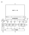
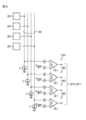
- the load current source unit 13 is composed of a set of a plurality of load current sources I (see FIG. 2) connected to each of the signal lines 32 1 to 32 n for each pixel row.
- the load current source I is composed of, for example, a MOS type field effect transistor (FET), and each of the signal lines 32 1 to 32 n for each pixel 20 of the pixel row selectively scanned by the row selection unit 12. Bias current is supplied through.
- FET MOS type field effect transistor
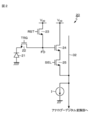
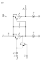
- a transfer signal TRG in which a high level (for example, V DD level) is active is given to the gate electrode of the transfer transistor 22 from the row selection unit 12.
- the transfer transistor 22 becomes conductive in response to the transfer signal TRG, is photoelectrically converted by the photodiode 21, and transfers the optical charge stored in the photodiode 21 to the floating diffusion FD.
- the reset transistor 23 is connected between the node of the high potential side power supply voltage V DD and the floating diffusion FD.
- a reset signal RST that activates a high level is given to the gate electrode of the reset transistor 23 from the row selection unit 12.
- the reset transistor 23 becomes conductive in response to the reset signal RST, and resets the floating diffusion FD by discarding the charge of the floating diffusion FD to the node of the voltage V DD.
- the pixel 20 is composed of a transfer transistor 22, a reset transistor 23, an amplification transistor 24, and a selection transistor 25, that is, a 4Tr configuration composed of four transistors (Tr) is given as an example.
- the selection transistor 25 may be omitted, and the amplification transistor 24 may have a 3Tr configuration in which the function of the selection transistor 25 is provided. If necessary, the number of transistors may be increased to a configuration of 5Tr or more. ..
- the comparator 141 uses the analog pixel signal V VSL read from the pixel 20 as a comparison input and the reference signal V RAMP of the lamp wave generated by the reference signal generation unit 17 as a reference input, and compares both signals. Then, for example, when the reference signal V RAMP is larger than the pixel signal V VSL , the output of the comparator 141 is in the first state (for example, high level), and when the reference signal V RAMP is equal to or less than the pixel signal V VSL. The output is in the second state (eg, low level). As a result, the comparator 141 outputs a pulse signal having a pulse width corresponding to the signal level of the pixel signal VVSL, specifically, the magnitude of the signal level, as a comparison result.
- comparator 141 of the analog-to-digital converter 140 As the comparator 141 of the analog-to-digital converter 140, a comparator having various configurations can be used. Hereinafter, a specific circuit configuration example of the comparator that can be used as the comparator 141 of the analog-to-digital converter 140 will be described.
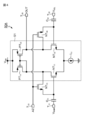
- the common connection node N 11 between the second differential transistor NT 12 and the second load transistor PT 12 is an output node of the differential amplifier 51, and the output signal OUT from the output node through the output terminal T 10. Is derived.
- Each source electrode of the first load transistor PT 11 and the second load transistor PT 12 is connected to a node of the power supply voltage V DD.
- the first switch transistor NT 13 is connected between the gate electrode and the drain electrode of the first differential transistor NT 11.
- the second switch transistor NT 14 is connected between the gate electrode and the drain electrode of the second differential transistor NT 12.
- the first switch transistor NT 13 and the second switch transistor NT 14 are turned on (conducting) / off (non-conducting) by the drive signal AZ input from the timing control unit 16 shown in FIG. 1 via the input terminal T 13. By being controlled, auto-zero (initialization operation) is selectively performed.
- FIG. 5 is a circuit diagram showing the circuit configuration of the comparator according to the circuit configuration example 2.
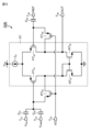
- the comparator 50B according to the circuit configuration example 2 includes a differential amplifier 51, a first capacitive element C 21 , a second capacitive element C 22 , a third capacitive element C 23 , a first switch transistor PT 23 , and It is configured to include a second switch transistor PT 24.
- the third capacitive element C 23 is connected between the gate electrode of the second differential transistor PT 22 and the input terminal T 24 of a predetermined voltage REF.
- the second differential transistor PT 22 takes a predetermined voltage REF applied through the terminal T 24 as a gate input via the third capacitive element C 23.
- the predetermined voltage REF is an arbitrary constant voltage such as a power supply voltage V DD and a GND (ground) level.
- the predetermined voltage REF is set to the GND level.
- the input voltage of the differential amplifier 51 at the time of inverting the output signal OUT of the differential amplifier 51 does not fluctuate and is constant regardless of the signal amount of the pixel 20. Therefore, it is possible to reduce the power supply voltage VDD (for example, about 1.3V). As a result, the power consumption of the analog-to-digital conversion unit 14 can be reduced, so that the power consumption of the CMOS image sensor 1A can be reduced.
- VDD for example, about 1.3V
- the input transistor PT 41 is composed of a P-channel MOS transistor and is connected between the signal line 32 and the input side load current source I 41. Specifically, the source electrode of the input transistor PT 41 is connected to the signal line 32, and the drain electrode is connected to one end of the input side load current source I 41. As a result, the pixel signal VVSL is input to the source electrode of the input transistor PT 41 through the signal line 32.
- the input transistor PT 41 amplifies the difference between the reference signal V RAMP input to the gate electrode and the pixel signal V VSL input to the source electrode, that is, the gate-source voltage V gs of the input transistor PT 41. It is output as a drain voltage from the drain electrode. In the input transistor PT 41 , it is desirable that the back gate electrode and the source electrode are short-circuited in order to suppress the back gate effect.
- the circuit configuration of the comparator 50D according to the circuit configuration example 4 exemplified here is an example, and is not limited to this circuit configuration.
- the circuit configuration of the subsequent input transistor PT 41 for example, suppressing clamp transistor lowering the drain voltage when the non-conductive state of the input transistor PT 41, provided in parallel to the input transistor PT 41 It can be configured.
- the clamp transistor to limit the lower limit of the drain voltage of the input transistor PT 41 it can be configured to provided in parallel to the input transistor PT 41.
- the pixel array unit 11 in which the pixels 20 are arranged in a matrix is divided into, for example, two regions 11A and 11B in the column direction.
- the signal lines 32 are the first signal line 32A (32A 1 to 32A n ) and the second signal line 32B (32B 1 to) in the length direction (column direction) for each pixel row. It is divided into 32B n).
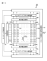
- the two divided regions 11A and 11B of the pixel array unit 11 in which the pixels 20 are two-dimensionally arranged in a matrix form electricity with the semiconductor chip 42 of the second layer. It is formed so as to sandwich the connection portions (VIA) 54A and 54B for making a target connection. Further, for example, pads 51 for external connection and power supply are provided at both left and right ends of the first layer semiconductor chip 41.
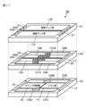
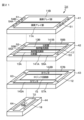
- the analog circuit unit of the analog-to-digital conversion unit 14, specifically, the comparators 141A and 141B of the analog-to-digital converter 140 are arranged on the semiconductor chip 42 of the second layer. Further, the load current source portions 13A and 13B are arranged on the second layer semiconductor chip 42 with the connection portions (VIA) 55A and 55B for electrical connection with the first layer semiconductor chip 41 interposed therebetween.
- the arrangement of the comparators 141A and 141B of the analog-to-digital converter 140 on the second layer semiconductor chip 42 shown in FIG. 11, the load current source units 13A and 13B, and the reference signal generation unit 17 is an example. Therefore, it is not limited to this arrangement example.
- the comparators 141A and 141B arranged on the second layer semiconductor chip 42 corresponding to the two regions 11A and 11B and the counters 142A and 142B arranged on the third layer semiconductor chip 43 are two layers. It is electrically connected for each pixel row through the connection portions 56A and 56B of the eyes and the connection portions 57A and 57B of the third layer.
- Examples of the connecting portions 54A and 54B, the connecting portions 55A and 55B, the connecting portions 56A and 56B, and the connecting portions 57A and 57B include a through silicon via (TSV), a metal-metal junction including a Cu-Cu junction, and the like. Can be done.
- TSV through silicon via
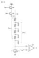
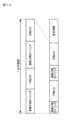
- FIG. 14 shows a timing diagram for one horizontal period (1H). If the parasitic resistance R VSL and the parasitic capacitance C VSL can be halved, the pixel P-phase / D-phase settling time (signal line potential settling time) can be shortened, so that the time required to read the pixel signal of one line can be shortened, and the frame can be shortened. The rate can be improved. Further, since the settling time can be shortened and a free time is generated within one horizontal period as shown in FIG. 14, power consumption can be reduced by stopping the circuit operation during the free time. Alternatively, the current I LM flowing through the load current source I may be reduced by the amount that the parasitic resistance R VSL and the parasitic capacitance C VSL are reduced while maintaining the same one horizontal period without shortening the settling time. ..
- FIG. 15 is a block diagram schematically showing an outline of a system configuration of a CMOS image sensor which is an example of an image pickup apparatus according to a third embodiment to which the technique according to the present disclosure is applied.
- the CMOS image sensor 1C according to the third embodiment also has the same as the case of the CMOS image sensor 1A according to the first embodiment, the first layer semiconductor chip 41 and the second layer semiconductor chip 42. And, it has a laminated chip structure in which at least three semiconductor chips of the third layer semiconductor chip 43 are laminated.
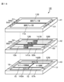
- the analog circuit unit of the analog-to-digital conversion unit 14, specifically, the comparators 141A and 141B of the analog-to-digital converter 140 are arranged on the semiconductor chip 43 of the third layer. On the outside of the comparators 141A and 141B, connection portions 57A and 57B for electrically connecting to the second layer semiconductor chip 42 are provided.
- the laminated chip structure is a three-layer laminated structure
- the laminated structure is not limited to the three-layer laminated structure, and may be a four-layer or more laminated structure.
- the analog circuit unit and the digital circuit unit of the analog-to-digital conversion unit 14 can be distributed and arranged on the semiconductor chips of the second and subsequent layers.
- a process suitable for manufacturing the digital circuit unit of the analog-to-digital conversion unit 14 (for example, a 22 nm process) can be applied to the semiconductor chip 42 of the second layer, and the three layers can be applied. Since a low-cost process (for example, a 55 nm process) suitable for manufacturing the analog circuit unit of the analog-to-digital converter 14 can be applied to the semiconductor chip 43 of the eye, the characteristics and cost can be optimized. In particular, advanced processes can be applied to the production of digital circuit units.
- the interface 18 is provided on the semiconductor chip 42 of the second layer, the interface 18 is provided as compared with the case where the interface 18 is provided on the semiconductor chip 43 of the third layer. It is possible to reduce the parasitic resistance and the parasitic capacitance attached to the output of.
- the output of the interface 18 is a high-speed signal, and it is important in design that the parasitic resistance and the parasitic capacitance for one layer can be reduced.
- the first layer semiconductor chip 41 and the second layer The configuration of the semiconductor chip 42 of the eye is the same as that of the CMOS image sensor 1B according to the second embodiment.
- the CMOS image sensor 1F includes a first-layer semiconductor chip 41, a second-layer semiconductor chip 42, a third-layer semiconductor chip 43, and a fourth-layer semiconductor. It has a laminated chip structure in which four semiconductor chips of the chip 44 are laminated.
- the configurations of the first-layer semiconductor chip 41, the second-layer semiconductor chip 42, and the third-layer semiconductor chip 43 are the same as in the case of the CMOS image sensor 1B according to the second embodiment. That is, the semiconductor chip 41 of the first layer is formed with two divided regions 11A, 11B, etc. of the pixel array unit 11, and the semiconductor chip 42 of the second layer is a comparator of the analog-digital converter 140. 141A, 141B, load current source units 13A, 13B, reference signal generation unit 17, and the like are arranged. The first-layer semiconductor chip 41 and the second-layer semiconductor chip 42 are electrically connected to each other through the first-layer connection portions 54A and 54B and the second-layer connection portions 55A and 55B.
- a memory unit 71 and an interface 18 are arranged on the semiconductor chip 44 of the fourth layer.
- the semiconductor chip 43 of the third layer and the semiconductor chip 44 of the fourth layer are connected by, for example, CoW (Chip on Wafer).
- the logic circuit unit 15 on the third-layer semiconductor chip 43 and the memory unit 71 on the fourth-layer semiconductor chip 44 are electrically connected to each other through the third-layer connection unit 63 and the fourth-layer connection unit 64. Will be done.
- the memory unit 71 can be used, for example, in the logic circuit unit 15 to temporarily hold data in the process of desired signal processing.
- the CMOS image sensor 1G according to the seventh embodiment also has the same as the CMOS image sensor 1E according to the sixth embodiment, the first layer semiconductor chip 41, the second layer semiconductor chip 42, and 3. It has a laminated chip structure in which four semiconductor chips of the semiconductor chip 43 of the layer and the semiconductor chip 44 of the fourth layer are laminated.
- an advanced process for example, a 12 nm process
- the size of the semiconductor chip 44 of the fourth layer is smaller than the size of the other semiconductor chips 41, 42, 43, many semiconductor chips 44 can be manufactured from one wafer, so that the cost can be reduced. Can be done.
- the image pickup optical system 101 takes in incident light (image light) from the subject and forms an image on the image pickup surface of the image pickup unit 102.
- the image pickup unit 102 converts the amount of incident light imaged on the image pickup surface by the optical system 101 into an electric signal in pixel units and outputs it as a pixel signal.
- the DSP circuit 103 performs general camera signal processing, for example, white balance processing, demosaic processing, gamma correction processing, and the like.
- the operation system 107 issues operation commands for various functions of the image pickup apparatus 100 under the operation of the user.
- the power supply system 108 appropriately supplies various power sources that serve as operating power sources for the DSP circuit 103, the frame memory 104, the display device 105, the recording device 106, and the operation system 107 to these supply targets.
- the body system control unit 12020 controls the operation of various devices mounted on the vehicle body according to various programs.
- the body system control unit 12020 functions as a keyless entry system, a smart key system, a power window device, or a control device for various lamps such as headlamps, back lamps, brake lamps, turn signals or fog lamps.
- the body system control unit 12020 may be input with radio waves transmitted from a portable device that substitutes for the key or signals of various switches.
- the body system control unit 12020 receives inputs of these radio waves or signals and controls a vehicle door lock device, a power window device, a lamp, and the like.
- the vehicle outside information detection unit 12030 detects information outside the vehicle equipped with the vehicle control system 12000.
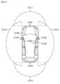
- the image pickup unit 12031 is connected to the vehicle outside information detection unit 12030.
- the vehicle outside information detection unit 12030 causes the image pickup unit 12031 to capture an image of the outside of the vehicle and receives the captured image.
- the out-of-vehicle information detection unit 12030 may perform object detection processing or distance detection processing such as a person, a vehicle, an obstacle, a sign, or a character on the road surface based on the received image.
- the in-vehicle information detection unit 12040 detects the in-vehicle information.
- a driver state detection unit 12041 that detects the driver's state is connected to the in-vehicle information detection unit 12040.
- the driver state detection unit 12041 includes, for example, a camera that images the driver, and the in-vehicle information detection unit 12040 determines the degree of fatigue or concentration of the driver based on the detection information input from the driver state detection unit 12041. It may be calculated, or it may be determined whether the driver has fallen asleep.
- the microcomputer 12051 controls the driving force generating device, the steering mechanism, the braking device, and the like based on the information around the vehicle acquired by the vehicle exterior information detection unit 12030 or the vehicle interior information detection unit 12040. It is possible to perform coordinated control for the purpose of automatic driving that runs autonomously without depending on the operation.
Landscapes
- Engineering & Computer Science (AREA)
- Multimedia (AREA)
- Signal Processing (AREA)
- Transforming Light Signals Into Electric Signals (AREA)
- Solid State Image Pick-Up Elements (AREA)
Abstract
Description
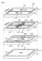
1層目の半導体チップ、2層目の半導体チップ、及び、3層目の半導体チップの少なくとも3つの半導体チップが積層された積層チップ構造を有し、
1層目の半導体チップには、画素が行列状に2次元配置されて成る画素アレイ部が形成されており、
2層目の半導体チップ及び3層目の半導体チップの一方には、画素アレイ部の各画素から信号線を通して読み出されるアナログの画素信号をデジタルの画素信号に変換するアナログ-デジタル変換部のアナログ回路部が配置されており、
2層目の半導体チップ及び3層目の半導体チップの他方には、アナログ-デジタル変換部のデジタル回路部が配置されている。
1.本開示の撮像装置及び電子機器、全般に関する説明
2.第1実施形態に係る撮像装置
2-1.CMOSイメージセンサの構成例
2-2.画素の回路構成例
2-3.アナログ-デジタル変換部の構成例
2-4.比較器の回路構成例
2-4-1.回路構成例1
2-4-2.回路構成例2
2-4-3.回路構成例3
2-4-4.回路構成例4
2-5.積層チップ構造
3.第2実施形態に係る撮像装置
3-1.CMOSイメージセンサの構成例
3-2.積層チップ構造
3-3.半導体チップ間の電気的接続構造
3-3-1.電気的接続構造例1
3-3-2.電気的接続構造例2
4.第3実施形態に係る撮像装置
4-1.CMOSイメージセンサの構成例
4-2.積層チップ構造
5.第4実施形態に係る撮像装置
6.第5実施形態に係る撮像装置
7.第6実施形態に係る撮像装置
8.第7実施形態に係る撮像装置
9.第8実施形態に係る撮像装置
10.変形例
11.応用例
12.本開示に係る技術の適用例
12-1.本開示の電子機器(撮像システムの例)
12-2.移動体への応用例
13.本開示がとることができる構成
本開示の撮像装置及び電子機器にあっては、アナログ-デジタル変換部について、画素アレイ部の画素列に対応して設けられた複数のアナログ-デジタル変換器から成り、アナログ-デジタル変換器について、アナログの画素信号とランプ波の参照信号とを比較する比較器、及び、参照信号の発生タイミングから、アナログの画素信号とランプ波の参照信号とが交差するまでの時間を計測するカウンタを有する構成とすることができる。そして、2層目の半導体チップ及び3層目の半導体チップの一方には、アナログ-デジタル変換部の比較器が配置されており、2層目の半導体チップ及び3層目の半導体チップの他方には、アナログ-デジタル変換部のカウンタが配置されている構成とすることができる。
本開示に係る技術が適用される第1実施形態に係る撮像装置として、X-Yアドレス方式の撮像装置の一種であるCMOS(Complementary Metal Oxide Semiconductor)イメージセンサを例に挙げて説明する。この点については、後述する実施形態においても同様である。CMOSイメージセンサは、CMOSプロセスを応用して、又は、部分的に使用して作製されたイメージセンサである。
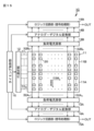
図1は、本開示に係る技術が適用される第1実施形態に係る撮像装置の一例であるCMOSイメージセンサのシステム構成の概略を模式的に示すブロック図である。
図2は、画素20の回路構成の一例を示す回路図である。画素20は、受光素子である光電変換素子として、例えば、フォトダイオード21を有している。画素20は、フォトダイオード21の他に、転送トランジスタ22、リセットトランジスタ23、増幅トランジスタ24、及び、選択トランジスタ25を有する構成となっている。
続いて、アナログ-デジタル変換部14の構成の一例について説明する。ここでは、アナログ-デジタル変換部14の各アナログ-デジタル変換器として、シングルスロープ型アナログ-デジタル変換器を用いる場合を例に挙げて説明する。
アナログ-デジタル変換器140の比較器141としては、種々の構成の比較器を用いることができる。以下に、アナログ-デジタル変換器140の比較器141として用いることができる比較器の具体的な回路構成例について説明する。
図4は、回路構成例1に係る比較器の回路構成を示す回路図である。回路構成例1に係る比較器50Aは、差動アンプ51、第1の容量素子C11、第2の容量素子C12、第1のスイッチトランジスタNT13、及び、第2のスイッチトランジスタNT14を備える構成となっている。
図5は、回路構成例2に係る比較器の回路構成を示す回路図である。回路構成例2に係る比較器50Bは、差動アンプ51、第1の容量素子C21、第2の容量素子C22、第3の容量素子C23、第1のスイッチトランジスタPT23、及び、第2のスイッチトランジスタPT24を備える構成となっている。
図6は、回路構成例3に係る比較器の回路構成を示す回路図である。回路構成例3に係る比較器50Cは、第1の容量素子C31、第2の容量素子C32、入力トランジスタPT31、スイッチトランジスタPT32、第1の電流源トランジスタNT31、及び、第2の電流源トランジスタNT32を備える構成となっている。
図7は、回路構成例4に係る比較器の回路構成を示す回路図である。回路構成例4に係る比較器50Dは、第1の容量素子C41、入力トランジスタPT41、入力側負荷電流源I41、第2の容量素子C42、出力トランジスタPT42、出力側負荷電流源I42、及び、スイッチトランジスタPT43を備える構成となっている。
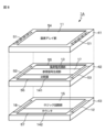
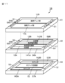
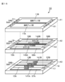
第1実施形態に係るCMOSイメージセンサ1Aは、1層目の半導体チップ、2層目の半導体チップ、及び、3層目の半導体チップの少なくとも3つの半導体チップが積層された積層チップ構造を有している。第1実施形態に係るCMOSイメージセンサ1Aの積層チップ構造の模式的な分解斜視図を図8に示す。
本開示に係る技術が適用される第2実施形態に係る撮像装置は、第1実施形態の場合と同様に、CMOSイメージセンサから成る。そして、画素アレイ部11が、列方向において複数の領域、例えば2つの領域に分割され、これに対応して信号線32が、長さ方向(列方向)において、複数の信号線に分断(例えば、2分割)された構成となっている。
図10は、本開示に係る技術が適用される第2実施形態に係る撮像装置の一例であるCMOSイメージセンサのシステム構成の概略を模式的に示すブロック図である。
第2実施形態に係るCMOSイメージセンサ1Bの積層チップ構造の模式的な分解斜視図を図11に示す。
続いて、1層目の半導体チップ41-2層目の半導体チップ42間、及び、2層目の半導体チップ42-3層目の半導体チップ43間の電気的接続構造について説明する。
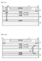
半導体チップ間の電気的接続構造例1の場合の切断部端面図を図12Aに示す。電気的接続構造例1は、半導体チップ間の電気的接続部としてシリコン貫通電極(TSV)を用いる例である。図12Aに示すように、画素アレイ部(画素領域)11が形成された1層目の半導体チップ41の左右両端部には、外部接続用や電源用のパッド51用の開口61が形成されている。
半導体チップ間の電気的接続構造例2の場合の切断部端面図を図12Bに示す。電気的接続構造例2では、1層目の半導体チップ41-2層目の半導体チップ42間の画素アレイ部11中の接続部54A(54B)-55A(55B)として、Cu-Cu接合を用いている。2層目の半導体チップ42-3層目の半導体チップ43間の画素アレイ部11外の接続部については、シリコン貫通電極62を用いてもよいし、Cu-Cu接合を用いてもよい。
第2実施形態に係る撮像装置は、2層目の半導体チップ42にアナログ-デジタル変換部14のアナログ回路部を形成し、3層目の半導体チップ43にアナログ-デジタル変換部14のデジタル回路部を形成した構成となっている。これに対し、第3実施形態に係る撮像装置は、2層目の半導体チップ42にアナログ-デジタル変換部14のデジタル回路部を形成し、3層目の半導体チップ43にアナログ-デジタル変換部14のアナログ回路部を形成した構成となっている。
図15は、本開示に係る技術が適用される第3実施形態に係る撮像装置の一例であるCMOSイメージセンサのシステム構成の概略を模式的に示すブロック図である。
第3実施形態に係るCMOSイメージセンサ1Cの積層チップ構造の模式的な分解斜視図を図16に示す。
第4実施形態は、第2実施形態の変形例であり、3層目の半導体チップにメモリ領域を確保する例である。
第5実施形態は、第4実施形態の変形例であり、3層目の半導体チップにメモリ領域に代えて、AI(Artificial Intelligence)領域を確保する例である。
第6実施形態は、第2実施形態の変形例であり、積層チップ構造が4層の積層構造の例である。
第7実施形態は、第6実施形態の変形例であり、4層目の半導体チップにメモリ領域に代えて、AI領域を確保する例である。
第8実施形態は、第7実施形態の変形例であり、4層目の半導体チップのサイズを他のの半導体チップのサイズよりも小さくした例である。
以上、本開示に係る技術について、好ましい実施形態に基づき説明したが、本開示に係る技術は当該実施形態に限定されるものではない。上記の実施形態において説明した撮像装置の構成、構造は例示であり、適宜、変更することができる。
以上説明した本実施形態に係る撮像装置は、例えば図22に示すように、可視光、赤外光、紫外光、X線等の光をセンシングする様々な装置に使用することができる。様々な装置の具体例について以下に列挙する。
・自動停止等の安全運転や、運転者の状態の認識等のために、自動車の前方や後方、周囲、車内等を撮影する車載用センサ、走行車両や道路を監視する監視カメラ、車両間等の測距を行う測距センサ等の、交通の用に供される装置
・ユーザのジェスチャを撮影して、そのジェスチャに従った機器操作を行うために、TVや、冷蔵庫、エアーコンディショナ等の家電に供される装置
・内視鏡や、赤外光の受光による血管撮影を行う装置等の、医療やヘルスケアの用に供される装置
・防犯用途の監視カメラや、人物認証用途のカメラ等の、セキュリティの用に供される装置
・肌を撮影する肌測定器や、頭皮を撮影するマイクロスコープ等の、美容の用に供され装置
・スポーツ用途等向けのアクションカメラやウェアラブルカメラ等の、スポーツの用に供される装置
・畑や作物の状態を監視するためのカメラ等の、農業の用に供される装置
本開示に係る技術は、様々な製品に適用することができる。以下に、より具体的な適用例について説明する。
ここでは、デジタルスチルカメラやビデオカメラ等の撮像システムや、携帯電話機などの撮像機能を有する携帯端末装置や、画像読取部に撮像装置を用いる複写機などの電子機器に適用する場合について説明する。
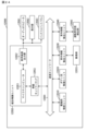
図23は、本開示の電子機器の一例である撮像システムの構成例を示すブロック図である。
本開示に係る技術(本技術)は、様々な製品へ応用することができる。例えば、本開示に係る技術は、自動車、電気自動車、ハイブリッド電気自動車、自動二輪車、自転車、パーソナルモビリティ、飛行機、ドローン、船舶、ロボット、建設機械、農業機械(トラクター)などのいずれかの種類の移動体に搭載される撮像装置として実現されてもよい。
尚、本開示は、以下のような構成をとることもできる。
[A-01]
1層目の半導体チップ、2層目の半導体チップ、及び、3層目の半導体チップの少なくとも3つの半導体チップが積層された積層チップ構造を有し、
1層目の半導体チップには、画素が行列状に2次元配置されて成る画素アレイ部が形成されており、
2層目の半導体チップ及び3層目の半導体チップの一方には、画素アレイ部の各画素から信号線を通して読み出されるアナログの画素信号をデジタルの画素信号に変換するアナログ-デジタル変換部のアナログ回路部が配置されており、
2層目の半導体チップ及び3層目の半導体チップの他方には、アナログ-デジタル変換部のデジタル回路部が配置されている、
撮像装置。
[A-02]
アナログ-デジタル変換部は、画素アレイ部の画素列に対応して設けられた複数のアナログ-デジタル変換器から成り、
アナログ-デジタル変換器は、
アナログの画素信号とランプ波の参照信号とを比較する比較器、及び、
参照信号の発生タイミングから、アナログの画素信号とランプ波の参照信号とが交差するまでの時間を計測するカウンタを有し、
2層目の半導体チップ及び3層目の半導体チップの一方には、アナログ-デジタル変換部の比較器が配置されており、
2層目の半導体チップ及び3層目の半導体チップの他方には、アナログ-デジタル変換部のカウンタが配置されている、
上記[A-01]に記載の撮像装置。
[A-03]
2層目の半導体チップには、アナログ-デジタル変換部の比較器、及び、信号線に接続された負荷電流源が配置されており、
3層目の半導体チップには、アナログ-デジタル変換部のカウンタ、ロジック回路部、及び、インタフェースが配置されている、
上記[A-02]に記載の撮像装置。
[A-04]
3層目の半導体チップには、アナログ-デジタル変換部のカウンタ、ロジック回路部、及び、インタフェースの他に、メモリ部が配置されている、
上記[A-03]に記載の撮像装置。
[A-05]
3層目の半導体チップには、アナログ-デジタル変換部のカウンタ、ロジック回路部、及び、インタフェースの他に、AI回路が配置されている、
上記[A-03]に記載の撮像装置。
[A-06]
4層目の半導体チップを有し、
4層目の半導体チップには、メモリ部が配置されている、
上記[A-03]に記載の撮像装置。
[A-07]
4層目の半導体チップを有し、
4層目の半導体チップには、AI回路が配置されている、
上記[A-03]に記載の撮像装置。
[A-08]
4層目の半導体チップは、サイズが他の層の半導体チップのサイズよりも小さい、
上記[A-07]に記載の撮像装置。
[A-09]
2層目の半導体チップには、アナログ-デジタル変換部のカウンタ、ロジック回路部、及び、インタフェースが配置されており、
3層目の半導体チップには、アナログ-デジタル変換部の比較器、及び、信号線に接続された負荷電流源が配置されている、
上記[A-02]に記載の撮像装置。
[A-10]
アナログ-デジタル変換部は、画素アレイ部の複数の画素行の各画素から並列的に読み出されるアナログの画素信号のそれぞれをデジタルの画素信号に変換する、第1のアナログ-デジタル変換部及び第2のアナログ-デジタル変換部を含む複数系統のアナログ-デジタル変換部から成る、
上記[A-01]乃至上記[A-09]のいずれかに記載の撮像装置。
[A-11]
信号線は、その長さ方向において、画素列毎に、複数系統のアナログ-デジタル変換部に対応して、第1の信号線及び第2の信号線を含む複数の信号線に分断されている、
上記[A-10]に記載の撮像装置。
[A-12]
第1の信号線と第1のアナログ-デジタル変換部とを接続する第1の接続部、及び、第2の信号線と第2のアナログ-デジタル変換部とを接続する第2の接続部は、画素アレイ部の領域内に近接して設けられている、
上記[A-11]に記載の撮像装置。
[A-13]
第1の接続部及び第2の接続部は、Cu電極を用いた直接接合により、1層目の半導体チップと2層目の半導体チップとを接続する、
上記[A-12]に記載の撮像装置。
[B-01]
1層目の半導体チップ、2層目の半導体チップ、及び、3層目の半導体チップの少なくとも3つの半導体チップが積層された積層チップ構造を有し、
1層目の半導体チップには、画素が行列状に2次元配置されて成る画素アレイ部が形成されており、
2層目の半導体チップ及び3層目の半導体チップの一方には、画素アレイ部の各画素から信号線を通して読み出されるアナログの画素信号をデジタルの画素信号に変換するアナログ-デジタル変換部のアナログ回路部が配置されており、
2層目の半導体チップ及び3層目の半導体チップの他方には、アナログ-デジタル変換部のデジタル回路部が配置されている、
撮像装置を有する電子機器。
[B-02]
アナログ-デジタル変換部は、画素アレイ部の画素列に対応して設けられた複数のアナログ-デジタル変換器から成り、
アナログ-デジタル変換器は、
アナログの画素信号とランプ波の参照信号とを比較する比較器、及び、
参照信号の発生タイミングから、アナログの画素信号とランプ波の参照信号とが交差するまでの時間を計測するカウンタを有し、
2層目の半導体チップ及び3層目の半導体チップの一方には、アナログ-デジタル変換部の比較器が配置されており、
2層目の半導体チップ及び3層目の半導体チップの他方には、アナログ-デジタル変換部のカウンタが配置されている、
上記[B-01]に記載の電子機器。
[B-03]
2層目の半導体チップには、アナログ-デジタル変換部の比較器、及び、信号線に接続された負荷電流源が配置されており、
3層目の半導体チップには、アナログ-デジタル変換部のカウンタ、ロジック回路部、及び、インタフェースが配置されている、
上記[B-02]に記載の電子機器。
[B-04]
3層目の半導体チップには、アナログ-デジタル変換部のカウンタ、ロジック回路部、及び、インタフェースの他に、メモリ部が配置されている、
上記[B-03]に記載の電子機器。
[B-05]
3層目の半導体チップには、アナログ-デジタル変換部のカウンタ、ロジック回路部、及び、インタフェースの他に、AI回路が配置されている、
上記[B-03]に記載の電子機器。
[B-06]
4層目の半導体チップを有し、
4層目の半導体チップには、メモリ部が配置されている、
上記[B-03]に記載の電子機器。
[B-07]
4層目の半導体チップを有し、
4層目の半導体チップには、AI回路が配置されている、
上記[B-03]に記載の電子機器。
[B-08]
4層目の半導体チップは、サイズが他の層の半導体チップのサイズよりも小さい、
上記[B-07]に記載の電子機器。
[B-09]
2層目の半導体チップには、アナログ-デジタル変換部のカウンタ、ロジック回路部、及び、インタフェースが配置されており、
3層目の半導体チップには、アナログ-デジタル変換部の比較器、及び、信号線に接続された負荷電流源が配置されている、
上記[B-02]に記載の電子機器。
[B-10]
アナログ-デジタル変換部は、画素アレイ部の複数の画素行の各画素から並列的に読み出されるアナログの画素信号のそれぞれをデジタルの画素信号に変換する、第1のアナログ-デジタル変換部及び第2のアナログ-デジタル変換部を含む複数系統のアナログ-デジタル変換部から成る、
上記[B-01]乃至上記[B-09]のいずれかに記載の電子機器。
[B-11]
信号線は、その長さ方向において、画素列毎に、複数系統のアナログ-デジタル変換部に対応して、第1の信号線及び第2の信号線を含む複数の信号線に分断されている、
上記[B-10]に記載の電子機器。
[B-12]
第1の信号線と第1のアナログ-デジタル変換部とを接続する第1の接続部、及び、第2の信号線と第2のアナログ-デジタル変換部とを接続する第2の接続部は、画素アレイ部の領域内に近接して設けられている、
上記[B-11]に記載の電子機器。
[B-13]
第1の接続部及び第2の接続部は、Cu電極を用いた直接接合により、1層目の半導体チップと2層目の半導体チップとを接続する、
上記[B-12]に記載の電子機器。
Claims (14)
- 1層目の半導体チップ、2層目の半導体チップ、及び、3層目の半導体チップの少なくとも3つの半導体チップが積層された積層チップ構造を有し、
1層目の半導体チップには、画素が行列状に2次元配置されて成る画素アレイ部が形成されており、
2層目の半導体チップ及び3層目の半導体チップの一方には、画素アレイ部の各画素から信号線を通して読み出されるアナログの画素信号をデジタルの画素信号に変換するアナログ-デジタル変換部のアナログ回路部が配置されており、
2層目の半導体チップ及び3層目の半導体チップの他方には、アナログ-デジタル変換部のデジタル回路部が配置されている、
撮像装置。 - アナログ-デジタル変換部は、画素アレイ部の画素列に対応して設けられた複数のアナログ-デジタル変換器から成り、
アナログ-デジタル変換器は、
アナログの画素信号とランプ波の参照信号とを比較する比較器、及び、
参照信号の発生タイミングから、アナログの画素信号とランプ波の参照信号とが交差するまでの時間を計測するカウンタを有し、
2層目の半導体チップ及び3層目の半導体チップの一方には、アナログ-デジタル変換部の比較器が配置されており、
2層目の半導体チップ及び3層目の半導体チップの他方には、アナログ-デジタル変換部のカウンタが配置されている、
請求項1に記載の撮像装置。 - 2層目の半導体チップには、アナログ-デジタル変換部の比較器、及び、信号線に接続された負荷電流源が配置されており、
3層目の半導体チップには、アナログ-デジタル変換部のカウンタ、ロジック回路部、及び、インタフェースが配置されている、
請求項2に記載の撮像装置。 - 3層目の半導体チップには、アナログ-デジタル変換部のカウンタ、ロジック回路部、及び、インタフェースの他に、メモリ部が配置されている、
請求項3に記載の撮像装置。 - 3層目の半導体チップには、アナログ-デジタル変換部のカウンタ、ロジック回路部、及び、インタフェースの他に、AI回路が配置されている、
請求項3に記載の撮像装置。 - 4層目の半導体チップを有し、
4層目の半導体チップには、メモリ部が配置されている、
請求項3に記載の撮像装置。 - 4層目の半導体チップを有し、
4層目の半導体チップには、AI回路が配置されている、
請求項3に記載の撮像装置。 - 4層目の半導体チップは、サイズが他の層の半導体チップのサイズよりも小さい、
請求項7に記載の撮像装置。 - 2層目の半導体チップには、アナログ-デジタル変換部のカウンタ、ロジック回路部、及び、インタフェースが配置されており、
3層目の半導体チップには、アナログ-デジタル変換部の比較器、及び、信号線に接続された負荷電流源が配置されている、
請求項2に記載の撮像装置。 - アナログ-デジタル変換部は、画素アレイ部の複数の画素行の各画素から並列的に読み出されるアナログの画素信号のそれぞれをデジタルの画素信号に変換する、第1のアナログ-デジタル変換部及び第2のアナログ-デジタル変換部を含む複数系統のアナログ-デジタル変換部から成る、
請求項1に記載の撮像装置。 - 信号線は、その長さ方向において、画素列毎に、複数系統のアナログ-デジタル変換部に対応して、第1の信号線及び第2の信号線を含む複数の信号線に分断されている、
請求項10に記載の撮像装置。 - 第1の信号線と第1のアナログ-デジタル変換部とを接続する第1の接続部、及び、第2の信号線と第2のアナログ-デジタル変換部とを接続する第2の接続部は、画素アレイ部の領域内に近接して設けられている、
請求項11に記載の撮像装置。 - 第1の接続部及び第2の接続部は、Cu電極を用いた直接接合により、1層目の半導体チップと2層目の半導体チップとを接続する、
請求項12に記載の撮像装置。 - 1層目の半導体チップ、2層目の半導体チップ、及び、3層目の半導体チップの少なくとも3つの半導体チップが積層された積層チップ構造を有し、
1層目の半導体チップには、画素が行列状に2次元配置されて成る画素アレイ部が形成されており、
2層目の半導体チップ及び3層目の半導体チップの一方には、画素アレイ部の各画素から信号線を通して読み出されるアナログの画素信号をデジタルの画素信号に変換するアナログ-デジタル変換部のアナログ回路部が配置されており、
2層目の半導体チップ及び3層目の半導体チップの他方には、アナログ-デジタル変換部のデジタル回路部が配置されている、
撮像装置を有する電子機器。
Priority Applications (7)
| Application Number | Priority Date | Filing Date | Title |
|---|---|---|---|
| KR1020237003041A KR20230035058A (ko) | 2020-07-07 | 2021-05-19 | 촬상 장치 및 전자기기 |
| CN202512002030.7A CN121967922A (zh) | 2020-07-07 | 2021-05-19 | 摄像装置和电子设备 |
| US17/928,478 US12185012B2 (en) | 2020-07-07 | 2021-05-19 | Imaging device and electronic apparatus |
| JP2022534930A JP7695245B2 (ja) | 2020-07-07 | 2021-05-19 | 撮像装置及び電子機器 |
| EP21838841.1A EP4181502A4 (en) | 2020-07-07 | 2021-05-19 | IMAGING DEVICE AND ELECTRONIC DEVICE |
| CN202180037056.2A CN115699793B (zh) | 2020-07-07 | 2021-05-19 | 摄像装置和电子设备 |
| US18/954,853 US20250193557A1 (en) | 2020-07-07 | 2024-11-21 | Imaging device and electronic apparatus |
Applications Claiming Priority (2)
| Application Number | Priority Date | Filing Date | Title |
|---|---|---|---|
| JP2020-116898 | 2020-07-07 | ||
| JP2020116898 | 2020-07-07 |
Related Child Applications (2)
| Application Number | Title | Priority Date | Filing Date |
|---|---|---|---|
| US17/928,478 A-371-Of-International US12185012B2 (en) | 2020-07-07 | 2021-05-19 | Imaging device and electronic apparatus |
| US18/954,853 Continuation US20250193557A1 (en) | 2020-07-07 | 2024-11-21 | Imaging device and electronic apparatus |
Publications (1)
| Publication Number | Publication Date |
|---|---|
| WO2022009530A1 true WO2022009530A1 (ja) | 2022-01-13 |
Family
ID=79552861
Family Applications (1)
| Application Number | Title | Priority Date | Filing Date |
|---|---|---|---|
| PCT/JP2021/018890 Ceased WO2022009530A1 (ja) | 2020-07-07 | 2021-05-19 | 撮像装置及び電子機器 |
Country Status (7)
| Country | Link |
|---|---|
| US (2) | US12185012B2 (ja) |
| EP (1) | EP4181502A4 (ja) |
| JP (1) | JP7695245B2 (ja) |
| KR (1) | KR20230035058A (ja) |
| CN (2) | CN115699793B (ja) |
| TW (1) | TWI895446B (ja) |
| WO (1) | WO2022009530A1 (ja) |
Cited By (1)
| Publication number | Priority date | Publication date | Assignee | Title |
|---|---|---|---|---|
| WO2024214526A1 (ja) * | 2023-04-12 | 2024-10-17 | ソニーセミコンダクタソリューションズ株式会社 | 撮像装置 |
Families Citing this family (3)
| Publication number | Priority date | Publication date | Assignee | Title |
|---|---|---|---|---|
| EP4181502A4 (en) * | 2020-07-07 | 2023-08-16 | Sony Semiconductor Solutions Corporation | IMAGING DEVICE AND ELECTRONIC DEVICE |
| JP2022038476A (ja) * | 2020-08-26 | 2022-03-10 | ソニーセミコンダクタソリューションズ株式会社 | 撮像装置および電子機器 |
| JP2022119375A (ja) * | 2021-02-04 | 2022-08-17 | キヤノン株式会社 | 光電変換装置 |
Citations (8)
| Publication number | Priority date | Publication date | Assignee | Title |
|---|---|---|---|---|
| JP2013179313A (ja) * | 2005-06-02 | 2013-09-09 | Sony Corp | 半導体イメージセンサ・モジュール |
| WO2014007004A1 (ja) | 2012-07-06 | 2014-01-09 | ソニー株式会社 | 固体撮像装置及び固体撮像装置の駆動方法、並びに、電子機器 |
| WO2015159728A1 (ja) * | 2014-04-15 | 2015-10-22 | ソニー株式会社 | 撮像素子、電子機器 |
| JP2018148567A (ja) * | 2018-04-26 | 2018-09-20 | ソニー株式会社 | 半導体装置、固体撮像装置、およびカメラシステム |
| WO2019087764A1 (ja) * | 2017-10-30 | 2019-05-09 | ソニーセミコンダクタソリューションズ株式会社 | 裏面照射型の固体撮像装置、および裏面照射型の固体撮像装置の製造方法、撮像装置、並びに電子機器 |
| WO2019124113A1 (ja) * | 2017-12-21 | 2019-06-27 | ソニーセミコンダクタソリューションズ株式会社 | 電磁波処理装置 |
| JP2020072410A (ja) * | 2018-10-31 | 2020-05-07 | ソニーセミコンダクタソリューションズ株式会社 | 固体撮像装置及び電子機器 |
| JP2020102816A (ja) * | 2018-12-25 | 2020-07-02 | キヤノン株式会社 | 撮像装置および撮像装置の制御方法 |
Family Cites Families (11)
| Publication number | Priority date | Publication date | Assignee | Title |
|---|---|---|---|---|
| JP4349232B2 (ja) * | 2004-07-30 | 2009-10-21 | ソニー株式会社 | 半導体モジュール及びmos型固体撮像装置 |
| EP3018894A1 (en) | 2014-11-06 | 2016-05-11 | IMEC vzw | Image sensor |
| JP2017117828A (ja) * | 2015-12-21 | 2017-06-29 | ソニー株式会社 | 固体撮像素子および電子装置 |
| JP6939568B2 (ja) * | 2016-01-15 | 2021-09-22 | ソニーグループ株式会社 | 半導体装置および撮像装置 |
| WO2018117662A1 (en) * | 2016-12-22 | 2018-06-28 | Samsung Electronics Co., Ltd. | Apparatus and method for processing image |
| US20180220093A1 (en) * | 2017-02-01 | 2018-08-02 | Renesas Electronics Corporation | Image sensor |
| WO2018142707A1 (ja) * | 2017-02-01 | 2018-08-09 | ソニーセミコンダクタソリューションズ株式会社 | 撮像システム及び撮像装置 |
| JP6953274B2 (ja) * | 2017-02-01 | 2021-10-27 | ソニーセミコンダクタソリューションズ株式会社 | 撮像システム及び撮像装置 |
| WO2019087597A1 (ja) | 2017-11-06 | 2019-05-09 | ソニーセミコンダクタソリューションズ株式会社 | 電圧変換回路、固体撮像素子および電圧変換回路の制御方法 |
| JP7286309B2 (ja) * | 2018-12-18 | 2023-06-05 | キヤノン株式会社 | 光電変換装置、光電変換システムおよび信号処理装置 |
| EP4181502A4 (en) * | 2020-07-07 | 2023-08-16 | Sony Semiconductor Solutions Corporation | IMAGING DEVICE AND ELECTRONIC DEVICE |
-
2021
- 2021-05-19 EP EP21838841.1A patent/EP4181502A4/en active Pending
- 2021-05-19 JP JP2022534930A patent/JP7695245B2/ja active Active
- 2021-05-19 CN CN202180037056.2A patent/CN115699793B/zh active Active
- 2021-05-19 US US17/928,478 patent/US12185012B2/en active Active
- 2021-05-19 CN CN202512002030.7A patent/CN121967922A/zh active Pending
- 2021-05-19 WO PCT/JP2021/018890 patent/WO2022009530A1/ja not_active Ceased
- 2021-05-19 KR KR1020237003041A patent/KR20230035058A/ko active Pending
- 2021-06-18 TW TW110122284A patent/TWI895446B/zh active
-
2024
- 2024-11-21 US US18/954,853 patent/US20250193557A1/en active Pending
Patent Citations (8)
| Publication number | Priority date | Publication date | Assignee | Title |
|---|---|---|---|---|
| JP2013179313A (ja) * | 2005-06-02 | 2013-09-09 | Sony Corp | 半導体イメージセンサ・モジュール |
| WO2014007004A1 (ja) | 2012-07-06 | 2014-01-09 | ソニー株式会社 | 固体撮像装置及び固体撮像装置の駆動方法、並びに、電子機器 |
| WO2015159728A1 (ja) * | 2014-04-15 | 2015-10-22 | ソニー株式会社 | 撮像素子、電子機器 |
| WO2019087764A1 (ja) * | 2017-10-30 | 2019-05-09 | ソニーセミコンダクタソリューションズ株式会社 | 裏面照射型の固体撮像装置、および裏面照射型の固体撮像装置の製造方法、撮像装置、並びに電子機器 |
| WO2019124113A1 (ja) * | 2017-12-21 | 2019-06-27 | ソニーセミコンダクタソリューションズ株式会社 | 電磁波処理装置 |
| JP2018148567A (ja) * | 2018-04-26 | 2018-09-20 | ソニー株式会社 | 半導体装置、固体撮像装置、およびカメラシステム |
| JP2020072410A (ja) * | 2018-10-31 | 2020-05-07 | ソニーセミコンダクタソリューションズ株式会社 | 固体撮像装置及び電子機器 |
| JP2020102816A (ja) * | 2018-12-25 | 2020-07-02 | キヤノン株式会社 | 撮像装置および撮像装置の制御方法 |
Non-Patent Citations (1)
| Title |
|---|
| See also references of EP4181502A4 |
Cited By (1)
| Publication number | Priority date | Publication date | Assignee | Title |
|---|---|---|---|---|
| WO2024214526A1 (ja) * | 2023-04-12 | 2024-10-17 | ソニーセミコンダクタソリューションズ株式会社 | 撮像装置 |
Also Published As
| Publication number | Publication date |
|---|---|
| US20230209227A1 (en) | 2023-06-29 |
| JP7695245B2 (ja) | 2025-06-18 |
| JPWO2022009530A1 (ja) | 2022-01-13 |
| US20250193557A1 (en) | 2025-06-12 |
| US12185012B2 (en) | 2024-12-31 |
| TW202205848A (zh) | 2022-02-01 |
| CN115699793A (zh) | 2023-02-03 |
| KR20230035058A (ko) | 2023-03-10 |
| EP4181502A1 (en) | 2023-05-17 |
| CN115699793B (zh) | 2025-12-16 |
| CN121967922A (zh) | 2026-05-01 |
| EP4181502A4 (en) | 2023-08-16 |
| TWI895446B (zh) | 2025-09-01 |
Similar Documents
| Publication | Publication Date | Title |
|---|---|---|
| KR102520518B1 (ko) | 촬상 소자, 촬상 소자의 제어 방법, 및 전자기기 | |
| JP7695245B2 (ja) | 撮像装置及び電子機器 | |
| JP7331180B2 (ja) | 撮像素子及び電子機器 | |
| JP7659385B2 (ja) | 撮像装置及び電子機器 | |
| JP7098346B2 (ja) | 撮像装置および撮像システム | |
| JP2022017676A (ja) | 撮像装置及び電子機器 | |
| TW202147826A (zh) | 固態攝像元件 | |
| WO2022030207A1 (ja) | 撮像装置及び電子機器 | |
| JP7242551B2 (ja) | 撮像装置 | |
| TW202103486A (zh) | 固態攝像裝置、電子機器及固態攝像裝置之控制方法 | |
| TW202320535A (zh) | 攝像裝置 | |
| JP2019134318A (ja) | 撮像装置およびキャリブレーション方法 | |
| US11381764B2 (en) | Sensor element and electronic device | |
| WO2022118630A1 (ja) | 撮像装置及び電子機器 | |
| WO2021157263A1 (ja) | 撮像装置及び電子機器 | |
| US12587756B2 (en) | Imaging device and electronic apparatus | |
| CN116195268A (zh) | 固态摄像装置 |
Legal Events
| Date | Code | Title | Description |
|---|---|---|---|
| 121 | Ep: the epo has been informed by wipo that ep was designated in this application |
Ref document number: 21838841 Country of ref document: EP Kind code of ref document: A1 |
|
| ENP | Entry into the national phase |
Ref document number: 2022534930 Country of ref document: JP Kind code of ref document: A |
|
| ENP | Entry into the national phase |
Ref document number: 20237003041 Country of ref document: KR Kind code of ref document: A |
|
| NENP | Non-entry into the national phase |
Ref country code: DE |
|
| ENP | Entry into the national phase |
Ref document number: 2021838841 Country of ref document: EP Effective date: 20230207 |