WO2022019299A1 - 電極 - Google Patents
電極 Download PDFInfo
- Publication number
- WO2022019299A1 WO2022019299A1 PCT/JP2021/027108 JP2021027108W WO2022019299A1 WO 2022019299 A1 WO2022019299 A1 WO 2022019299A1 JP 2021027108 W JP2021027108 W JP 2021027108W WO 2022019299 A1 WO2022019299 A1 WO 2022019299A1
- Authority
- WO
- WIPO (PCT)
- Prior art keywords
- electrode
- layer
- oxide layer
- metal
- conductive carbon
- Prior art date
- Legal status (The legal status is an assumption and is not a legal conclusion. Google has not performed a legal analysis and makes no representation as to the accuracy of the status listed.)
- Ceased
Links
Images


Classifications
-
- G—PHYSICS
- G01—MEASURING; TESTING
- G01N—INVESTIGATING OR ANALYSING MATERIALS BY DETERMINING THEIR CHEMICAL OR PHYSICAL PROPERTIES
- G01N27/00—Investigating or analysing materials by the use of electric, electrochemical, or magnetic means
- G01N27/26—Investigating or analysing materials by the use of electric, electrochemical, or magnetic means by investigating electrochemical variables; by using electrolysis or electrophoresis
- G01N27/28—Electrolytic cell components
- G01N27/30—Electrodes, e.g. test electrodes; Half-cells
- G01N27/308—Electrodes, e.g. test electrodes; Half-cells at least partially made of carbon
Definitions
- the present invention relates to electrodes.
- the titanium thin film improves the conductivity and the chemical stability in a short time.
- the electrode may be immersed in the electrolytic solution for a long period of time.
- the electrodes are required to suppress damage in the above cases. That is, the electrode is required to have excellent electrolyte durability.
- Patent Document 1 has a problem that it does not have the above-mentioned excellent electrolyte durability.
- the present invention provides an electrode having excellent electrolyte durability.
- the present invention (1) includes an electrode including a base film, an inorganic oxide layer, a metal base layer, and a conductive carbon layer in order toward one side in the thickness direction.
- the present invention (2) includes the electrode according to (1), wherein the metal underlayer is capable of forming carbon and carbides of the conductive carbon layer.
- the present invention (3) includes the electrode according to (1) or (2), wherein the inorganic oxide layer is a metal oxide layer or a metalloid oxide layer.
- the present invention (4) includes the electrode according to (3), wherein the metal oxide layer and the metal underlayer contain the same metal element.
- the present invention (5) includes the electrode according to (4), wherein the metal element is titanium.
- the present invention (6) includes the electrode according to any one of (3) to (5), wherein the metalloid oxide layer contains silicon dioxide.
- the present invention (7) includes the electrode according to any one of (1) to (6), wherein the thickness of the metal oxide layer is 5 nm or more.
- the present invention (8) includes the electrode according to any one of (1) to (7), which is an electrode for electrochemical measurement.
- the electrode of the present invention has excellent electrolyte durability.
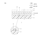
- FIG. 1 is a cross-sectional view of an embodiment of the electrode of the present invention.
- FIG. 2 is a cross-sectional view of an electrode in which a pinhole is formed.
- FIG. 3 is a cross-sectional view of the electrode of Comparative Example 1.
- FIG. 4 is a cross-sectional view of the electrode of Comparative Example 2.
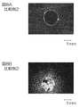
- 5A to 5B are OM images of the electrodes of Example 1.
- FIG. 5A shows the electrodes before being immersed in the electrolytic solution.
- FIG. 5B shows the electrodes after being immersed in the electrolytic solution.
- 6A to 6B are OM images of the electrodes of the second embodiment.
- FIG. 6A shows the electrodes before being immersed in the electrolytic solution.
- FIG. 6B shows the electrodes after being immersed in the electrolytic solution.
- FIG. 7A to 7B are OM images of the electrodes of Comparative Example 1.
- FIG. 7A shows an electrode before being immersed in the electrolytic solution.
- FIG. 7B shows an electrode after being immersed in the electrolytic solution.
- 8A to 8B are OM images of the electrodes of Comparative Example 2.
- FIG. 8A shows an electrode before being immersed in the electrolytic solution.
- FIG. 8B shows the electrodes after being immersed in the electrolytic solution.
- the electrode 1 has a predetermined thickness.
- the electrode 1 has a film shape (including a sheet shape).
- the electrode 1 includes a base film 2, an inorganic oxide layer 3, a metal base layer 4, and a conductive carbon layer 5 in this order toward one side in the thickness direction.
- the electrode 1 includes only the base film 2, the inorganic oxide layer 3, the metal base layer 4, and the conductive carbon layer 5.
- the base film 2 has a predetermined thickness.
- the material of the base film 2 include an inorganic material and an organic material. These can be used alone or in combination.
- Examples of the inorganic material include silicon and glass. These can be used alone or in combination.
- Examples of the organic material include a resin material.
- Examples of the resin material include polyester resin, acetate resin, polyether sulfone resin, polycarbonate resin, polyamide resin, polyimide resin, polyolefin resin, acrylic resin, polyvinyl chloride resin, polyvinylidene chloride resin, polystyrene resin, and polyvinyl alcohol resin. Examples thereof include polyarylate resin and polyphenylene sulfide resin. These can be used alone or in combination.
- the material of the base film 2 is preferably an organic material, and more preferably a polyester resin.
- the polyester resin include polyethylene terephthalate and polyethylene naphthalate.
- polyethylene terephthalate is preferable.
- the thickness of the base film 2 is not particularly limited.
- the thickness of the base film 2 is, for example, 2 ⁇ m or more, preferably 20 ⁇ m or more, and for example, 1000 ⁇ m or less, preferably 500 ⁇ m or less.
- the inorganic oxide layer 3 is arranged on one side of the base film 2 in the thickness direction. Specifically, the inorganic oxide layer 3 is in contact with all of one surface of the base film 2 in the thickness direction.
- the inorganic oxide layer 3 has a predetermined thickness.
- Examples of the inorganic oxide layer 3 include a metal oxide layer 3A or a metalloid oxide layer 3B.
- the metal oxide layer 3A is passivated.
- the passivation consists of metal oxides.
- the metal oxide include nickel oxide, cobalt oxide, chromium oxide, titanium oxide, aluminum oxide, tungsten oxide, molybdenum oxide, and composite oxides thereof. These can be used alone or in combination. Titanium oxide is preferably used from the viewpoint of further improving the durability of the electrolytic solution.
- the metalloid oxide layer 3B is made of a metalloid oxide.
- Metalloids are not limited. Examples of metalloids include silicon, antimony, germanium, and bismuth.
- the metalloid is preferably silicon.
- examples of metalloid oxides include silicon oxide, antimony oxide, germanium oxide, and bismuth oxide.
- examples of the metalloid oxide include glass such as borosilicate glass.
- silicon oxide is preferably used from the viewpoint of further improving the durability of the electrolytic solution. Examples of the silicon oxide include silicon dioxide (silica) and silicon monoxide, and silicon dioxide is preferable.
- the thickness of the inorganic oxide layer 3 is not particularly limited.
- the thickness of the inorganic oxide layer 3 is, for example, 1 nm or more, preferably 5 nm or more, more preferably 5 nm or more, and for example, 50 nm or less, preferably 25 nm or less.
- the inorganic oxide layer 3 is excellent in uniformity over the plane direction.
- the plane direction is a direction orthogonal to the thickness direction. Therefore, the inorganic oxide layer 3 becomes a continuous film, and the effect of improving the electrode durability can be expected.
- the inorganic oxide layer 3 is equal to or less than the above-mentioned upper limit, the inorganic oxide layer 3 (particularly, the metal oxide layer 3A) is also excellent in conductivity.
- the metal base layer 4 is arranged on one side of the inorganic oxide layer 3 in the thickness direction. Specifically, the metal base layer 4 is in contact with all of one surface of the inorganic oxide layer 3 in the thickness direction.
- the metal base layer 4 has a predetermined thickness.
- the material of the metal base layer 4 is metal.
- a metal is preferably capable of forming carbides with the carbon of the conductive carbon layer 5 described below.
- Specific examples of such metals include Group 2 elements in the periodic table, Group 4 to Group 14 elements, and alloys thereof. These can be used alone or in combination.
- metal base layer 4 and the metal oxide layer 3A contain, for example, the same metal element.
- Group 4 elements are preferably mentioned, and titanium and zirconium are more preferable. More preferably, titanium is mentioned.
- the metal oxide layer 3A and the metal base layer 4 contain titanium as an element.
- the metal oxide layer 3A and the metal base layer 4 are advantageous because the adhesion between the metal oxide layer 3A and the metal base layer 4 can be improved by including titanium.
- the material of the metal oxide layer 3A is titanium oxide.
- the material of the metal base layer 4 is titanium as a metal.
- the conductive carbon layer 5 is arranged on one side of the metal base layer 4 in the thickness direction. Specifically, the conductive carbon layer 5 is in contact with all of one surface of the metal base layer 4 in the thickness direction.
- the conductive carbon layer 5 has a predetermined thickness.
- the material of the conductive carbon layer 5 is carbon, preferably carbon having sp 2 and sp 3 bonds. Carbon with sp 2 and sp 3 bonds has a graphite-type structure and a diamond structure.
- the ratio of the number of atoms having sp 3 bonds to the sum of the number of atoms having sp 3 bonds and the number of atoms having sp 2 bonds (sp 3 / sp 3 + sp 2 ) is not particularly limited.
- the above-mentioned ratio (sp 3 / sp 3 + sp 2 ) is, for example, 0.1 or more, preferably 0.2 or more, and for example, 0.9 or less, preferably 0.5 or less.
- the ratio (sp 3 / sp 3 + sp 2 ) is the peak intensity of the sp 2 bond and the peak intensity of the sp 3 bond in the spectrum obtained by measuring one side of the conductive carbon layer 5 in the thickness direction by X-ray photoelectron spectroscopy. Calculated based on.
- the concentration ratio (O / C) of oxygen to carbon on one side of the conductive carbon layer 5 in the thickness direction is not particularly limited.
- the above-mentioned concentration ratio (O / C) is, for example, 0.15 or less, preferably 0.10 or less, and for example, 0.00 or more, 0.01 or more, or 0.02 or more. Furthermore, it is 0.03 or more.
- the concentration ratio is calculated based on the peak area of C1s and the peak area of O1s in the spectrum obtained by measuring one side of the conductive carbon layer 5 in the thickness direction by X-ray photoelectron spectroscopy.
- the surface resistance value of the conductive carbon layer 5 on one surface in the thickness direction is not particularly limited.
- the surface resistance of the conductive carbon layer 5 is, for example, 1.0 ⁇ 10 4 ⁇ / ⁇ or less, preferably 1.0 ⁇ 10 3 ⁇ / ⁇ or less.
- the surface resistance can be measured by the 4-terminal method according to JIS K 7194.
- the thickness of the conductive carbon layer 5 is not particularly limited.
- the thickness of the conductive carbon layer 5 is, for example, 5 nm or more, more preferably 10 nm or more, and for example, 200 nm or less, more preferably 100 nm or less.
- the thickness of the conductive carbon layer 5 is calculated by measuring the X-ray reflectance.
- a carbide layer (not shown) is preferably formed at the interface between the conductive carbon layer 5 and the metal base layer 4.
- the carbide layer is composed of a carbide which is a compound of the metal of the metal base layer 4 and the carbon of the conductive carbon layer 5.
- the carbide layer improves the adhesion between the conductive carbon layer 5 and the metal base layer 4.
- the electrode 1 includes a base film 2, an inorganic oxide layer 3, a metal base layer 4, a carbide layer (not shown), and a conductive carbon layer 5 in order toward one side in the thickness direction. ..
- the manufacturing method of the electrode 1 will be described.
- the base film 2 is prepared.
- the inorganic oxide layer 3, the metal base layer 4, and the conductive carbon layer 5 are sequentially formed on one side of the base film 2 in the thickness direction.
- Examples of the method for forming the inorganic oxide layer 3 include a dry method and a wet method.
- a dry method is preferable.
- Examples of the dry method include a PVD method (physical vapor deposition method) and a CVD method (chemical vapor deposition method).
- the PVD method is preferably mentioned.
- Examples of the PVD method include a sputtering method, a vacuum vapor deposition method, a laser vapor deposition method, and an ion plating method (arc vapor deposition method).
- the PVD method preferably includes a sputtering method.
- the sputtering method is not particularly limited.
- the sputtering method for example, an unbalanced magnetron sputtering method (UBM sputtering method), a high power pulse sputtering method, an electronic cyclotron resonance sputtering method, an RF sputtering method, a DC sputtering method (DC magnetron sputtering method), a DC pulse sputtering method. , And the ion beam sputtering method.
- UBM sputtering method unbalanced magnetron sputtering method
- a high power pulse sputtering method for example, an electronic cyclotron resonance sputtering method, an RF sputtering method, a DC sputtering method (DC magnetron sputtering method), a DC pulse sputtering method.
- DC magnetron sputtering method DC magnetron sputtering method
- DC pulse sputtering method a DC pulse sputtering method
- a sputtering gas containing oxygen and an inert gas and a target made of an inorganic substance are used.
- the inert gas examples include argon.
- the flow rate ratio of oxygen to the total flow rate of the sputtering gas is, for example, 0.01 or more, preferably 0.05, and for example, less than 0.5, preferably 0.2 or less.
- inorganic substances examples include metals and metalloids.
- Examples of the metal include metal elements that form metal oxides.
- Examples of the metal include nickel, cobalt, chromium, titanium, aluminum, tungsten, molybdenum, and alloys thereof. Titanium is preferably mentioned from the viewpoint of chemical stability.
- metalloid examples include the above-mentioned metalloids, preferably silicon.
- Examples of the method for forming the metal base layer 4 include the same method as the above-mentioned forming method for the inorganic oxide layer 3. However, when the metal base layer 4 is formed by the sputtering method, a sputtering gas containing only an inert gas without oxygen is used.
- the target material preferably, the same target material as the target material used in forming the metal oxide layer 3A can be mentioned, and more preferably, titanium can be mentioned. Since the target made of titanium can be shared between the formation of the metal oxide layer 3A and the formation of the metal base layer 4, the design of the manufacturing equipment becomes easy.
- Examples of the method for forming the conductive carbon layer 5 include the same method as the above-mentioned method for forming the inorganic oxide layer 3. However, when the conductive carbon layer 5 is formed by the sputtering method, a sputtering gas containing only an inert gas without oxygen is used. When the conductive carbon layer 5 is formed by a sputtering method, for example, carbon, preferably sintered carbon, is used as the target material. Then, if necessary, the conductive carbon layer 5 can be surface-treated.
- the electrode 1 is provided with the base film 2, the inorganic oxide layer 3, the metal base layer 4, and the conductive carbon layer 5 in order toward one side in the thickness direction, the electrode 1 is excellent in electrolytic solution durability. ..
- a pinhole 6 may be unavoidably formed on the electrode 1 due to its manufacture.
- the pinhole 6 is a hole that penetrates the inorganic oxide layer 3, the metal base layer 4, and the conductive carbon layer 5 in the thickness direction.
- the oxide layer 3, the metal base layer 4, and the conductive carbon layer 5 are formed. Since the adhesion between the foreign matter and the base film 2 is remarkably low, when the foreign matter is detached from one surface in the thickness direction of the base film 2, the inorganic oxide layer 3 and the metal base layer 4 are combined. The corresponding portion of the conductive carbon layer 5 and the conductive carbon layer 5 is also detached. As a result, the pinhole 6 described above is inevitably formed.
- the pinhole 6 is filled with the electrolytic solution.
- the electrolytic solution is based on the pinhole 6 and the metal base layer 4. It penetrates into the interface with the material film 2. Therefore, the metal base layer 4 is easily peeled off from one side of the base film 2 in the thickness direction. Therefore, the electrode 1 in FIG. 3 does not have sufficient durability of the electrolytic solution.
- the electrolytic solution durability means that the conductive carbon layer 5 is not easily damaged when the electrode 1 is immersed in the electrolytic solution for a long period of time.
- the electrolyte durability is defined when the electrode 1 is immersed in the electrolyte for, for example, 5 days or more, further 10 days or more, further 15 days or more, and further 20 days or more. This means that the conductive carbon layer 5 is not easily damaged.
- the metal base layer 4 comes into contact with one surface of the base film 2 in the thickness direction. ing. Therefore, as shown by the arrow in FIG. 4, the electrolytic solution penetrates from the pinhole 6 into the interface between the metal base layer 4 and the base film 2.
- the inorganic oxide layer 3 is provided between the metal base layer 4 and the base film 2. Has been done. Therefore, the inorganic oxide layer 3 can prevent the electrolytic solution from infiltrating between the metal base layer 4 and the base film 2. That is, the inorganic oxide layer 3 can function as a barrier layer against the electrolytic solution. Specifically, in the inorganic oxide layer 3, the inner peripheral surface 7 facing the pinhole 6 serves as a stopper portion.
- the electrolytic solution may infiltrate the interface between the conductive carbon layer 5 and the metal base layer 4 and peel off the conductive carbon layer 5 from the metal base layer 4.
- a carbide layer is formed at the interface between the conductive carbon layer 5 and the metal base layer 4. Therefore, the adhesive force between the conductive carbon layer 5 and the metal base layer 4 is improved, and the above-mentioned infiltration can be suppressed. Therefore, peeling of the conductive carbon layer 5 from the metal base layer 4 can be suppressed.
- the adhesion between the metal oxide layer 3A and the metal base layer 4 can be improved. Further, since the metal oxide layer 3A and the metal base layer 4 can use a target made of the same metal element, a common film forming chamber can be used. Therefore, the electrode 1 can be manufactured by a compact manufacturing facility.
- the metal oxide layer 3A and the metal base layer 4 both contain titanium as an element, the chemical stability of the electrode 1 is excellent. Further, since the target made of titanium is common in the formation of the metal oxide layer 3A and the formation of the metal base layer 4, the design of the manufacturing equipment becomes easy.
- the inorganic oxide layer 3 is a metalloid oxide layer 3B, therefore, it is effective for the metalloid oxide layer 3B to allow the electrolytic solution to penetrate between the metal base layer 4 and the base film 2. Can be suppressed. Therefore, the electrode 1 provided with the metalloid oxide layer 3B has excellent electrolyte durability.
- the thickness of the inorganic oxide layer 3 is 5 nm or more, the uniformity of the inorganic oxide layer 3 over the plane direction is excellent.
- the use of the electrode 1 is not particularly limited.
- Examples of the use of the electrode 1 include an electrode for electrochemical measurement. Specifically, it is provided in an electrochemical measurement system including an electrode 1 as a working electrode.
- Examples and comparative examples are shown below, and the present invention will be described in more detail.
- the present invention is not limited to Examples and Comparative Examples.
- specific numerical values such as the compounding ratio (content ratio), physical property values, parameters, etc. used in the following description are described in the above-mentioned "form for carrying out the invention", and the compounding ratios corresponding to them (Substitute the upper limit value (value defined as “less than or equal to” or “less than”) or the lower limit value (value defined as "greater than or equal to” or “excess”) such as content ratio), physical property value, parameter, etc. be able to.
- Example 1 A base film 2 having a thickness of 50 ⁇ m made of polyethylene terephthalate was prepared.
- a metal oxide layer 3A (inorganic oxide layer 3) made of titanium oxide was formed on one side of the base film 2 in the thickness direction.
- the conditions of the magnetron sputtering method are as follows.
- Target material Titanium Target power: 100W Sputtering gas: Argon and oxygen (flow ratio 9: 1) Sputtering chamber pressure: 0.2Pa The thickness of the metal oxide layer 3A was 5 nm.
- a metal base layer 4 made of titanium was formed on one side of the metal oxide layer 3A in the thickness direction.
- the conditions of the magnetron sputtering method are as follows.
- Titanium Target power 100W
- Sputtering gas Argon Sputtering chamber pressure: 0.2Pa
- the thickness of the metal base layer 4 was 12 nm.
- the conductive carbon layer 5 was formed on one surface of the metal base layer 4 in the thickness direction by the DC pulse sputtering method.
- the conditions of the DC pulse sputtering method are as follows.
- Target material Sintered carbon Argon gas pressure: 0.4 Pa
- Target power 3.3 W / cm 2
- Temperature 120 ° C or less
- the surface resistance of the conductive carbon layer 5 was 130 ⁇ / ⁇ .
- the ratio (sp 3 / sp 3 + sp 2 ) in the conductive carbon layer 5 was 0.35.
- the concentration ratio (O / C) of oxygen to carbon was 0.06.
- the thickness of the conductive carbon layer 5 was 30 nm.
- an electrode 1 having a base film 2, a metal oxide layer 3A, a metal base layer 4, and a conductive carbon layer 5 in order toward one side in the thickness direction was manufactured.
- Example 2 The treatment was carried out in the same manner as in Example 1 except that the thickness of the metal oxide layer 3A was changed to 2 nm.
- Example 3 The treatment was carried out in the same manner as in Example 1 except that the metalloid oxide layer 3B was formed instead of the metal oxide layer 3A. That is, a metalloid oxide layer 3B (inorganic oxide layer 3) made of silicon dioxide was formed on one side of the base film 2 in the thickness direction by a magnetron sputtering method.
- the conditions of the magnetron sputtering method are as follows.
- Target material Silicon Target power: 700W
- Sputtering gas Argon and oxygen (flow ratio, 7: 3)
- Sputtering pressure 0.3Pa
- the thickness of the metalloid oxide layer 3B was 10 nm.
- Example 4 The treatment was carried out in the same manner as in Example 1 except that the thickness of the metalloid oxide layer 3B was changed to 5 nm.
- Comparative Example 1 The treatment was carried out in the same manner as in Example 1 except that the metal oxide layer 3A was not formed. That is, as shown in FIG. 3, the electrode 1 is provided with the base film 2, the metal base layer 4, and the conductive carbon layer 5 in order toward one side in the thickness direction.
- Comparative Example 2 The treatment was carried out in the same manner as in Example 1 except that the formation order of the metal oxide layer 3A and the metal base layer 4 was changed. That is, as shown in FIG. 4, the electrode 1 includes a base film 2, a metal base layer 4, a metal oxide layer 3A, and a conductive carbon layer 5 in order toward one side in the thickness direction. ..
- an insulating tape 9 was attached to one surface of the conductive carbon layer 5 in the thickness direction.
- the insulating tape 9 has an opening 8 having a diameter of 2 mm.
- the electrode 1 and the insulating tape 9 were immersed in a 0.1 M nitric acid solution for 56 days.
- FIGS. 5A to 8B Optical microscope images (hereinafter referred to as OM image images) of the electrode 1 and the insulating tape 9 before and after immersion are shown in FIGS. 5A to 8B.
- 5 to 8 are Comparative Examples 1 to 2, respectively.
- FIG. 5A is the electrode 1 before immersion in Example 1.
- FIG. 5B is the electrode 1 after immersion in Example 1.
- 6A to 8B are the same as those of FIGS. 5A to 5B described above.
- the durability of the electrolytic solution was evaluated based on the following criteria.
- ⁇ As can be seen from FIG. 5B, almost no damaged portion due to pinhole formation was observed. ⁇ : As can be seen from FIG. 6B, a few damaged parts due to pinhole formation were observed. X: As can be seen from FIGS. 7B and 8B, damage spots due to pinhole formation were observed to a considerable extent.
- the potential window of the electrode 1 of each comparative example was measured using a potentiostat. Thereby, the electrode characteristic of the electrode 1 was evaluated.
- the potential window means a voltage range in which no current flows even when a voltage is applied, and the wider the range, the better the electrode characteristics of the electrode 1.
- Electrode 1 As a working electrode was constructed.
- This electrochemical measurement system includes an Ag / AgCl electrode as a reference electrode and a Pt electrode as a counter electrode.
- the electrode 1 was immersed in a 0.1 M sulfuric acid solution. Subsequently, the potential was swept with respect to the electrode 1, and the width of the potential when the potential reached 500 ⁇ A / cm 2 was defined as the potential window.
- Electrodes are used, for example, for electrochemical measurements.
- Electrode 2 Base film 3 Inorganic oxide layer 3A Metal oxide layer 3B Metalloid oxide layer 4 Metal base layer 5 Conductive carbon layer
Landscapes
- Chemical & Material Sciences (AREA)
- Life Sciences & Earth Sciences (AREA)
- Health & Medical Sciences (AREA)
- Biochemistry (AREA)
- General Physics & Mathematics (AREA)
- Electrochemistry (AREA)
- Physics & Mathematics (AREA)
- Analytical Chemistry (AREA)
- Molecular Biology (AREA)
- General Health & Medical Sciences (AREA)
- Chemical Kinetics & Catalysis (AREA)
- Immunology (AREA)
- Pathology (AREA)
- Hybrid Cells (AREA)
- Fuel Cell (AREA)
- Electrodes For Compound Or Non-Metal Manufacture (AREA)
- Battery Electrode And Active Subsutance (AREA)
- Laminated Bodies (AREA)
Abstract
Description
本発明の電極の一実施形態を、図1から図2を参照して説明する。
そして、この電極1は、基材フィルム2と、無機酸化物層3と、金属下地層4と、導電性カーボン層5とを厚み方向一方側に向かって順に備えるので、電解液耐久性に優れる。
電極1の用途は、特に限定されない。電極1の用途としては、例えば、電気化学測定用の電極が挙げられる。具体的には、電極1を作用電極として含む電気化学測定システムに備えられる。
ポリエチレンテレフタレートからなる厚み50μmの基材フィルム2を準備した。
ターゲットパワー:100W
スパッタリングガス:アルゴンと酸素(流量比で、9:1)
スパッタリング室の圧力:0.2Pa
金属酸化物層3Aの厚みは、5nmであった。
ターゲットパワー:100W
スパッタリングガス:アルゴン
スパッタリング室の圧力:0.2Pa
金属下地層4の厚みは、12nmであった。
ターゲット材:焼結カーボン
アルゴンガス圧:0.4Pa
ターゲットパワー:3.3W/cm2
温度:120℃以下
金属酸化物層3Aの厚みを2nmに変更した以外は、実施例1と同様に処理した。
金属酸化物層3Aに代えて、半金属酸化物層3Bを形成した以外は、実施例1と同様に処理した。すなわち、マグネトロンスパッタ法によって、二酸化ケイ素からなる半金属酸化物層3B(無機酸化物層3)を基材フィルム2の厚み方向一方面に形成した。マグネトロンスパッタリング法の条件は、以下の通りである。
ターゲットパワー:700W
スパッタリングガス:アルゴンと酸素(流量比で、7:3)
スパッタリングの圧力:0.3Pa
半金属酸化物層3Bの厚みは、10nmであった。
半金属酸化物層3Bの厚みを5nmに変更を形成した以外はした以外は、実施例1と同様に処理した。
金属酸化物層3Aを形成しなかった以外は、実施例1と同様に処理した。つまり、図3に示すように、この電極1は、基材フィルム2と、金属下地層4と、導電性カーボン層5とを厚み方向一方側に向かって順に備えた。
金属酸化物層3Aと、金属下地層4との形成順序を入れ替えた以外は、実施例1と同様に処理した。つまり、図4に示すように、この電極1は、基材フィルム2と、金属下地層4と、金属酸化物層3Aと、導電性カーボン層5とを厚み方向一方側に向かって順に備えた。
各実施例から各比較例の電極1について、次の事項を評価した。それらの結果を表1に示す。
導電性カーボン層5の厚み方向一方面に、図1、図3および図4のそれぞれの仮想線で示すように、絶縁テープ9を貼着した。絶縁テープ9は、直径が2mmである開口部8を有する。
△:図6Bから分かるように、ピンホール形成に起因する損傷箇所が、わずかに観察された。
×:図7Bおよび図8Bから分かるように、ピンホール形成に起因する損傷箇所が、相当程度、観察された。
各実施例から各比較例の電極1の電位窓を、ポテンショスタットを用いて測定した。これによって、電極1の電極特性を評価した。電位窓は、電圧をかけても電流が流れない電圧範囲を意味し、その範囲が広いほど、電極1の電極特性が良好であることを意味する。

2 基材フィルム
3 無機酸化物層
3A 金属酸化物層
3B 半金属酸化物層
4 金属下地層
5 導電性カーボン層
Claims (12)
- 基材フィルムと、無機酸化物層と、金属下地層と、導電性カーボン層とを厚み方向一方側に向かって順に備えることを特徴とする、電極。
- 前記金属下地層は、前記導電性カーボン層の炭素と炭化物を形成可能であることを特徴とする、請求項1に記載の電極。
- 前記無機酸化物層は、金属酸化物層または半金属酸化物層であることを特徴とする、請求項1または2に記載の電極。
- 前記金属酸化物層と、前記金属下地層とは、同一の金属元素を含むことを特徴とする、請求項3に記載の電極。
- 前記金属元素が、チタンであることを特徴とする、請求項4に記載の電極。
- 前記半金属酸化物層は、二酸化ケイ素を含むことを特徴とする、請求項3~5のいずれか一項に記載の電極。
- 前記無機酸化物層の厚みが、5nm以上であることを特徴とする、請求項1から5のいずれか一項に記載の電極。
- 前記無機酸化物層の厚みが、5nm以上であることを特徴とする、請求項6に記載の電極。
- 電気化学測定用の電極であることを特徴とする、請求項1~5のいずれか一項に記載の電極。
- 電気化学測定用の電極であることを特徴とする、請求項6に記載の電極。
- 電気化学測定用の電極であることを特徴とする、請求項7に記載の電極。
- 電気化学測定用の電極であることを特徴とする、請求項8に記載の電極。
Priority Applications (4)
| Application Number | Priority Date | Filing Date | Title |
|---|---|---|---|
| JP2022538018A JP7658973B2 (ja) | 2020-07-22 | 2021-07-20 | 電極 |
| EP21846785.0A EP4187239A4 (en) | 2020-07-22 | 2021-07-20 | ELECTRODE |
| CN202180060705.0A CN116134306A (zh) | 2020-07-22 | 2021-07-20 | 电极 |
| US18/017,389 US12578295B2 (en) | 2020-07-22 | 2021-07-20 | Electrode having carbon layer with SP3/SP2 bonding |
Applications Claiming Priority (2)
| Application Number | Priority Date | Filing Date | Title |
|---|---|---|---|
| JP2020125152 | 2020-07-22 | ||
| JP2020-125152 | 2020-07-22 |
Publications (1)
| Publication Number | Publication Date |
|---|---|
| WO2022019299A1 true WO2022019299A1 (ja) | 2022-01-27 |
Family
ID=79729157
Family Applications (1)
| Application Number | Title | Priority Date | Filing Date |
|---|---|---|---|
| PCT/JP2021/027108 Ceased WO2022019299A1 (ja) | 2020-07-22 | 2021-07-20 | 電極 |
Country Status (6)
| Country | Link |
|---|---|
| US (1) | US12578295B2 (ja) |
| EP (1) | EP4187239A4 (ja) |
| JP (1) | JP7658973B2 (ja) |
| CN (1) | CN116134306A (ja) |
| TW (1) | TWI899290B (ja) |
| WO (1) | WO2022019299A1 (ja) |
Cited By (1)
| Publication number | Priority date | Publication date | Assignee | Title |
|---|---|---|---|---|
| WO2024203071A1 (ja) | 2023-03-27 | 2024-10-03 | 日東電工株式会社 | 電極 |
Families Citing this family (1)
| Publication number | Priority date | Publication date | Assignee | Title |
|---|---|---|---|---|
| US12578295B2 (en) * | 2020-07-22 | 2026-03-17 | Nitto Denko Corporation | Electrode having carbon layer with SP3/SP2 bonding |
Citations (6)
| Publication number | Priority date | Publication date | Assignee | Title |
|---|---|---|---|---|
| JP2010204029A (ja) * | 2009-03-05 | 2010-09-16 | Kobe Steel Ltd | 中空構造素子 |
| JP2013185991A (ja) * | 2012-03-08 | 2013-09-19 | Dainippon Printing Co Ltd | 濃度測定センサ及びその製造方法 |
| US20140322608A1 (en) * | 2011-08-15 | 2014-10-30 | Purdue Research Foundation | Modified graphitic electrodes for electrochemical energy storage enhancement |
| WO2016013478A1 (ja) | 2014-07-22 | 2016-01-28 | 東洋紡株式会社 | 薄膜積層フィルム |
| JP2019105637A (ja) * | 2017-12-11 | 2019-06-27 | 日東電工株式会社 | 電極フィルムおよび電気化学測定システム |
| WO2021009845A1 (ja) * | 2019-07-16 | 2021-01-21 | 株式会社オプトラン | 電極及び電極チップ |
Family Cites Families (10)
| Publication number | Priority date | Publication date | Assignee | Title |
|---|---|---|---|---|
| KR101435999B1 (ko) * | 2007-12-07 | 2014-08-29 | 삼성전자주식회사 | 도펀트로 도핑된 산화그라펜의 환원물, 이를 포함하는 박막및 투명전극 |
| JP5353205B2 (ja) * | 2008-11-27 | 2013-11-27 | 日産自動車株式会社 | 導電部材、その製造方法、ならびにこれを用いた燃料電池用セパレータおよび固体高分子形燃料電池 |
| KR101119916B1 (ko) * | 2009-08-24 | 2012-03-13 | 삼성전자주식회사 | 그래핀 전극과 유기물/무기물 복합소재를 사용한 전자 소자 및 그 제조 방법 |
| WO2013126888A1 (en) * | 2012-02-23 | 2013-08-29 | Northwestern University | Nanostructured carbon electrode, methods of fabricating and applications of the same |
| CN107210092B (zh) * | 2015-03-04 | 2019-06-18 | 株式会社钟化 | 带导电层的基板、触摸面板用带透明电极的基板及它们的制造方法 |
| WO2018102175A1 (en) | 2016-11-30 | 2018-06-07 | Saint-Gobain Performance Plastics Corporation | Electrode and method for making an electrode |
| CN108232204A (zh) * | 2016-12-10 | 2018-06-29 | 中国科学院大连化学物理研究所 | 一种硅基有序化电极及其制备方法和应用 |
| CN107167507B (zh) * | 2017-05-16 | 2019-04-19 | 重庆石墨烯研究院有限公司 | 带dna分子探针的石墨烯微电极电化学检测传感器 |
| US12578295B2 (en) * | 2020-07-22 | 2026-03-17 | Nitto Denko Corporation | Electrode having carbon layer with SP3/SP2 bonding |
| US12344928B2 (en) * | 2021-03-23 | 2025-07-01 | Nitto Denko Corporation | Electrode and method of producing the electrode |
-
2021
- 2021-07-20 US US18/017,389 patent/US12578295B2/en active Active
- 2021-07-20 WO PCT/JP2021/027108 patent/WO2022019299A1/ja not_active Ceased
- 2021-07-20 JP JP2022538018A patent/JP7658973B2/ja active Active
- 2021-07-20 CN CN202180060705.0A patent/CN116134306A/zh active Pending
- 2021-07-20 EP EP21846785.0A patent/EP4187239A4/en active Pending
- 2021-07-22 TW TW110126958A patent/TWI899290B/zh active
Patent Citations (6)
| Publication number | Priority date | Publication date | Assignee | Title |
|---|---|---|---|---|
| JP2010204029A (ja) * | 2009-03-05 | 2010-09-16 | Kobe Steel Ltd | 中空構造素子 |
| US20140322608A1 (en) * | 2011-08-15 | 2014-10-30 | Purdue Research Foundation | Modified graphitic electrodes for electrochemical energy storage enhancement |
| JP2013185991A (ja) * | 2012-03-08 | 2013-09-19 | Dainippon Printing Co Ltd | 濃度測定センサ及びその製造方法 |
| WO2016013478A1 (ja) | 2014-07-22 | 2016-01-28 | 東洋紡株式会社 | 薄膜積層フィルム |
| JP2019105637A (ja) * | 2017-12-11 | 2019-06-27 | 日東電工株式会社 | 電極フィルムおよび電気化学測定システム |
| WO2021009845A1 (ja) * | 2019-07-16 | 2021-01-21 | 株式会社オプトラン | 電極及び電極チップ |
Non-Patent Citations (1)
| Title |
|---|
| See also references of EP4187239A4 |
Cited By (2)
| Publication number | Priority date | Publication date | Assignee | Title |
|---|---|---|---|---|
| WO2024203071A1 (ja) | 2023-03-27 | 2024-10-03 | 日東電工株式会社 | 電極 |
| EP4692775A1 (en) | 2023-03-27 | 2026-02-11 | Nitto Denko Corporation | Electrode |
Also Published As
| Publication number | Publication date |
|---|---|
| JPWO2022019299A1 (ja) | 2022-01-27 |
| TWI899290B (zh) | 2025-10-01 |
| TW202217298A (zh) | 2022-05-01 |
| US20230266263A1 (en) | 2023-08-24 |
| CN116134306A (zh) | 2023-05-16 |
| US12578295B2 (en) | 2026-03-17 |
| EP4187239A4 (en) | 2024-08-28 |
| EP4187239A1 (en) | 2023-05-31 |
| JP7658973B2 (ja) | 2025-04-08 |
Similar Documents
| Publication | Publication Date | Title |
|---|---|---|
| JP2019105637A (ja) | 電極フィルムおよび電気化学測定システム | |
| EP2157645B1 (en) | Metallic separator for fuel cell and process for producing the metallic separator | |
| EP2124278A1 (en) | Fuel cell separator, fuel cell separator manufacturing method and fuel cell | |
| JP7658973B2 (ja) | 電極 | |
| JP2010126801A (ja) | 錫被覆アルミニウム材料 | |
| CN115398217A (zh) | 电极 | |
| WO2019117112A1 (ja) | 電極フィルムおよび電気化学測定システム | |
| WO2016166935A1 (ja) | 固体高分子形燃料電池のセパレータ用金属板 | |
| TWI890866B (zh) | 電極 | |
| JP2009224152A (ja) | 透明電極、透明導電性基板および透明タッチパネル | |
| JP4516628B2 (ja) | 燃料電池用金属セパレータおよびその製造方法 | |
| US20140042017A1 (en) | Sensor elements with a tantalum- or niobium-containing base layer and methods of producing the same | |
| CN101287335A (zh) | 高导热电路基板 | |
| US20020127460A1 (en) | Protective coatings for fuel cell interconnect | |
| WO2024111533A1 (ja) | 配線基板およびその製造方法 | |
| JP2023152904A (ja) | 電極および電気化学測定システム | |
| WO2022210387A1 (ja) | 電極 | |
| WO2024203071A1 (ja) | 電極 | |
| WO2024180988A1 (ja) | 電極および電気化学測定システム | |
| JP7484760B2 (ja) | セパレータの製造方法 | |
| JP7352234B2 (ja) | 金属基板上に形成された薄膜の電気抵抗率の測定方法、並びに当該測定方法を利用する電子部品の製造方法及び電子部品の製造装置 | |
| WO2026063266A1 (ja) | 電極、電気化学センサー、バイオセンサーおよび電極の製造方法 | |
| WO2023153315A1 (ja) | 電極 | |
| JPH06228783A (ja) | 白金被膜電極及びその製造方法 |
Legal Events
| Date | Code | Title | Description |
|---|---|---|---|
| 121 | Ep: the epo has been informed by wipo that ep was designated in this application |
Ref document number: 21846785 Country of ref document: EP Kind code of ref document: A1 |
|
| ENP | Entry into the national phase |
Ref document number: 2022538018 Country of ref document: JP Kind code of ref document: A |
|
| NENP | Non-entry into the national phase |
Ref country code: DE |
|
| ENP | Entry into the national phase |
Ref document number: 2021846785 Country of ref document: EP Effective date: 20230222 |
|
| WWG | Wipo information: grant in national office |
Ref document number: 18017389 Country of ref document: US |