WO2022024907A1 - 回路基板およびその製造方法 - Google Patents
回路基板およびその製造方法 Download PDFInfo
- Publication number
- WO2022024907A1 WO2022024907A1 PCT/JP2021/027274 JP2021027274W WO2022024907A1 WO 2022024907 A1 WO2022024907 A1 WO 2022024907A1 JP 2021027274 W JP2021027274 W JP 2021027274W WO 2022024907 A1 WO2022024907 A1 WO 2022024907A1
- Authority
- WO
- WIPO (PCT)
- Prior art keywords
- metal
- main surface
- circuit board
- hole
- polishing
- Prior art date
- Legal status (The legal status is an assumption and is not a legal conclusion. Google has not performed a legal analysis and makes no representation as to the accuracy of the status listed.)
- Ceased
Links
Images


Classifications
-
- H—ELECTRICITY
- H05—ELECTRIC TECHNIQUES NOT OTHERWISE PROVIDED FOR
- H05K—PRINTED CIRCUITS; CASINGS OR CONSTRUCTIONAL DETAILS OF ELECTRIC APPARATUS; MANUFACTURE OF ASSEMBLAGES OF ELECTRICAL COMPONENTS
- H05K3/00—Apparatus or processes for manufacturing printed circuits
- H05K3/40—Forming printed elements for providing electric connections to or between printed circuits
- H05K3/42—Plated through-holes or plated via connections
- H05K3/425—Plated through-holes or plated via connections characterised by the sequence of steps for plating the through-holes or via connections in relation to the conductive pattern
- H05K3/426—Plated through-holes or plated via connections characterised by the sequence of steps for plating the through-holes or via connections in relation to the conductive pattern initial plating of through-holes in substrates without metal
-
- H—ELECTRICITY
- H05—ELECTRIC TECHNIQUES NOT OTHERWISE PROVIDED FOR
- H05K—PRINTED CIRCUITS; CASINGS OR CONSTRUCTIONAL DETAILS OF ELECTRIC APPARATUS; MANUFACTURE OF ASSEMBLAGES OF ELECTRICAL COMPONENTS
- H05K1/00—Printed circuits
- H05K1/02—Details
- H05K1/11—Printed elements for providing electric connections to or between printed circuits
- H05K1/115—Via connections; Lands around holes or via connections
-
- H—ELECTRICITY
- H05—ELECTRIC TECHNIQUES NOT OTHERWISE PROVIDED FOR
- H05K—PRINTED CIRCUITS; CASINGS OR CONSTRUCTIONAL DETAILS OF ELECTRIC APPARATUS; MANUFACTURE OF ASSEMBLAGES OF ELECTRICAL COMPONENTS
- H05K3/00—Apparatus or processes for manufacturing printed circuits
- H05K3/40—Forming printed elements for providing electric connections to or between printed circuits
- H05K3/42—Plated through-holes or plated via connections
- H05K3/423—Plated through-holes or plated via connections characterised by electroplating method
-
- H—ELECTRICITY
- H05—ELECTRIC TECHNIQUES NOT OTHERWISE PROVIDED FOR
- H05K—PRINTED CIRCUITS; CASINGS OR CONSTRUCTIONAL DETAILS OF ELECTRIC APPARATUS; MANUFACTURE OF ASSEMBLAGES OF ELECTRICAL COMPONENTS
- H05K2201/00—Indexing scheme relating to printed circuits covered by H05K1/00
- H05K2201/09—Shape and layout
- H05K2201/09209—Shape and layout details of conductors
- H05K2201/095—Conductive through-holes or vias
- H05K2201/09563—Metal filled via
-
- H—ELECTRICITY
- H05—ELECTRIC TECHNIQUES NOT OTHERWISE PROVIDED FOR
- H05K—PRINTED CIRCUITS; CASINGS OR CONSTRUCTIONAL DETAILS OF ELECTRIC APPARATUS; MANUFACTURE OF ASSEMBLAGES OF ELECTRICAL COMPONENTS
- H05K2203/00—Indexing scheme relating to apparatus or processes for manufacturing printed circuits covered by H05K3/00
- H05K2203/07—Treatments involving liquids, e.g. plating, rinsing
- H05K2203/0703—Plating
- H05K2203/0723—Electroplating, e.g. finish plating
-
- H—ELECTRICITY
- H05—ELECTRIC TECHNIQUES NOT OTHERWISE PROVIDED FOR
- H05K—PRINTED CIRCUITS; CASINGS OR CONSTRUCTIONAL DETAILS OF ELECTRIC APPARATUS; MANUFACTURE OF ASSEMBLAGES OF ELECTRICAL COMPONENTS
- H05K2203/00—Indexing scheme relating to apparatus or processes for manufacturing printed circuits covered by H05K3/00
- H05K2203/13—Moulding and encapsulation; Deposition techniques; Protective layers
- H05K2203/1377—Protective layers
- H05K2203/1394—Covering open PTHs, e.g. by dry film resist or by metal disc
-
- H—ELECTRICITY
- H05—ELECTRIC TECHNIQUES NOT OTHERWISE PROVIDED FOR
- H05K—PRINTED CIRCUITS; CASINGS OR CONSTRUCTIONAL DETAILS OF ELECTRIC APPARATUS; MANUFACTURE OF ASSEMBLAGES OF ELECTRICAL COMPONENTS
- H05K2203/00—Indexing scheme relating to apparatus or processes for manufacturing printed circuits covered by H05K3/00
- H05K2203/14—Related to the order of processing steps
- H05K2203/1476—Same or similar kind of process performed in phases, e.g. coarse patterning followed by fine patterning
Definitions
- the present invention relates to a circuit board and a method for manufacturing the same, and more particularly to a via metal that conducts through both main surfaces of an insulating substrate and a method for forming the via metal.
- a circuit board in which wirings formed on both main surfaces of an insulating substrate are connected by via metal penetrating both main surfaces is used. It is used.
- via metal either a method of forming a via hole in the insulating substrate and then filling it with metal, or filling a non-through hole formed from the first main surface of the insulating substrate with metal and then polishing the second main surface. It is formed by exposing the via metal.
- a method of filling the via hole or the non-through hole with metal a method by plating and a method of firing a paste containing metal particles are used (Patent Documents 1 to 3).
- JP-A-2015-43391A Japanese Unexamined Patent Publication No. 2006-66658 Japanese Unexamined Patent Publication No. 2001-291946
- the method for manufacturing a circuit board according to the present disclosure is a circuit board having an insulating substrate having a plurality of via holes penetrating the first main surface and the second main surface which are facing each other, and a metal filled with the via holes. It is a manufacturing method.
- the method for manufacturing a circuit board according to the present disclosure includes a hole forming step of forming a via hole or a non-through hole that opens only on the second main surface of the insulating substrate; and a filling step of filling the via hole or the non-through hole with the metal.
- a first polishing step of polishing at least one of the main surface metals to form a step between the metal and the insulating substrate; and a coating step of covering the polished surface of the metal by plating; 1 Includes a second polishing step of polishing the metal on the main surface and the second main surface.
- the circuit board of the present disclosure includes an insulating substrate having a plurality of via holes penetrating the first main surface and the second main surface which are facing main surfaces, a second metal layer filling the via holes, and a second metal. It has a third metal layer that covers the entire surface of the.
- the method using paste requires firing at a relatively high temperature. Therefore, thermal stress due to shrinkage after firing causes deformation and cracks.
- the firing temperature is higher than the melting point of the via metal, the influence of shrinkage due to the phase transformation is also added.
- the firing temperature is equal to or lower than the melting point of the metal, the metal becomes porous. As a result, many voids or glass components are contained in the metal, and it becomes difficult to reduce the surface roughness of the polished surface.
- the plating method can be formed at a relatively low temperature and is less likely to be deformed or cracked.
- a dense metal with few voids can be formed, and the surface roughness of the polished surface can be easily reduced.
- voids are likely to be formed near the center line where the metal grown from the inner wall surface of the via hole joins.
- Patent Document 3 also proposes a method of filling vias with a paste and covering with plating.
- the via metal formed by paste firing has the above-mentioned problems.
- the plating solution may remain in a large number of voids, which may adversely affect the characteristics of subsequent processes or products.
- circuit board that is dense, has a via metal with few voids on the surface, and is less likely to be deformed or cracked.
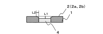
- the circuit board 10 has an insulating substrate 1 having a via hole 3 penetrating two opposing main surfaces 2 (first main surface 2a and a second main surface 2b), and a via metal 4 filling the via hole 3 (hereinafter, simply “. It may be described as “metal 4").
- the main surface 2 of the insulating substrate 1 and the surface of the via metal 4 are processed to have substantially the same height, and a wiring metal (not shown) connected to the via metal 4 is arranged on the main surface 2.
- the method for manufacturing the circuit board 10 of the present disclosure includes a hole forming step of forming a via hole 3 that opens in both main surfaces 2 or a non-through hole 6 that opens only in the second main surface 2b in the insulating substrate 1.
- FIG. 1 is a schematic diagram showing a first embodiment of the present disclosure.
- the first embodiment includes a hole forming step (FIG. 1A) for forming a via hole 3 in the insulating substrate 1; and a seed layer forming step (FIG. 1B) for forming a seed layer 5 on the first main surface 2a; by electroplating.
- a closing step (FIG. 1C) in which the first main surface 2a side of the via hole 3 is closed by the first metal layer 4a; and a filling step (FIG. 1D) in which the via hole 3 is filled with the second metal layer 4b by electroplating.
- a first polishing step (FIG.
- FIG. 1E shows an embodiment in which one main surface 2 (second main surface 2b) is polished in the first polishing step and both main surfaces 2 are polished in the second step.
- the insulating substrate 1 is made of ceramic, a single crystal, or the like, for example, sapphire. Sapphire is a single crystal of alumina.
- the dimensions of the insulating substrate 1 are, for example, a diameter of 50 mm or more and 200 mm or less, and a thickness of 0.2 mm or more and 1.0 mm or less.
- the via hole 3 is formed by a known method such as mechanical processing by a drill or the like, laser processing, etching, or the like. After drilling, heat treatment may be performed to alleviate crystal defects and stress caused by the drilling.
- the diameter of the via hole 3 is, for example, 100 ⁇ m or more and 500 ⁇ m or less.
- the material of the metal 4 is not particularly limited. Silver, copper, gold and alloys containing them as main components are suitable because of their high electrical conductivity. Platinum group elements, titanium, niobium, tantalum and alloys containing them as main components are suitable because they have high corrosion resistance.
- the third metal layer 4c is formed by electroplating.
- the first metal layer 4a and the second metal layer 4b are also preferably formed by electroplating, but may be formed by filling and firing a paste containing a metal component (in that case, forming the first metal layer 4a). Is unnecessary).
- Metal formation using paste requires firing at a relatively high temperature, and thermal stress due to shrinkage after firing causes deformation and cracks.
- the firing temperature is equal to or lower than the melting point of the metal, the metal becomes porous containing a large amount of voids and the surface roughness (arithmetic mean roughness) of the polished surface becomes large.
- the metal 4 can be formed by plating at a relatively low temperature, and is less likely to be deformed or cracked. A dense metal 4 with few voids can be formed, and the surface roughness of the polished surface can be easily reduced.
- the second metal layer 4b which is the main part of the metal 4
- the third metal layer 4c which is the surface of the metal 4, by plating, a dense and desired surface roughness surface can be obtained. Plating on a paste-fired metal with a large number of voids may cause residual plating solution, whereas plating on a plated metal with a small number of voids reduces such a concern.
- the seed layer 5 is formed on the first main surface 2a of the insulating substrate 1 by a method such as electroless plating or thin film deposition.
- the seed layer 5 is made of, for example, nickel, titanium, chromium, palladium or the like.
- Metal 4 is formed by electroplating starting from the seed layer 5.
- the seed layer 5 is used as a cathode, and an anode (metal source) is arranged on the first main surface 2a side.
- an anode metal source
- the first metal layer (closed layer) 4a is formed, and the first main surface 2a side of the via hole 3 is closed (closed step). Even if the via hole 3 is not completely closed, it may be closed until the opening area is about half or less of the cross-sectional area of the via hole 3.
- the first metal layer 4a is used as a cathode, and the anode is arranged on the second main surface 2b side. Then, as shown in FIG. 1D, a second metal layer (filled layer) 4b is formed and the via hole 3 is filled with the metal 4 (filling step).
- the film forming speed of the second metal layer 4b is higher than the film forming rate of the first metal 4a, it is preferable from the viewpoint of productivity. For example, the film forming speed can be increased by increasing the current density during electroplating.
- the packed bed 4b grows in the via hole 3 in the thickness direction (direction from the first main surface 2a toward the second main surface 2b) and also in the radial direction (direction from the inner wall surface toward the center line). Therefore, voids are likely to be formed in the vicinity of the center line where the grown metals 4 meet.
- the circuit board 10 if voids exist as open pores on the surface of the metal 4 or as closed pores near the surface, in the manufacturing process of the product using the circuit board 10, the wiring electrode It causes peeling. Further, the chemical solution used in the manufacturing process remains, which causes an adverse effect on the product.
- the second main surface 2b is polished using a lapping device or the like, and as shown in FIG. 1E, the metal 4 protruding from the second main surface 2b is removed (first polishing step).
- the metal 4 is softer and easier to polish than the insulating substrate 1 made of a ceramic such as alumina or an oxide single crystal such as sapphire. Therefore, a step L1 can be formed between the main surface 2 and the metal 4 after polishing (the surface of the metal 4 is lowered).
- the size of the step L1 can be adjusted by various conditions such as the material, shape, particle size of the abrasive grains, the pH of the slurry, the processing pressure, and the processing time.
- the surface of the metal 4 after polishing (that is, the interface between the second metal layer 4b and the third metal layer 4c) is flat and has a uniform surface roughness as compared with the non-polished surface.
- an anode is arranged on the polished surface side of the metal 4, and as shown in FIG. 1F, a third metal layer 4c is formed to cover the polished surface (coating step).
- the anode may be arranged on only one side. It is preferable that the third metal layer 4c is denser, that is, has less voids than the second metal layer 4b.
- the film forming speed of the third metal layer 4b is smaller than the film forming rate of the second metal 4b, the surface of the metal layer 4 is covered with a denser film, which is preferable. For example, by lowering the current density, the film forming speed can be reduced.
- the third metal layer 4c having a finer density or less voids, the open pores on the surface of the metal 4 and the closed pores near the surface can be used for subsequent processes and device performance.
- the adverse effect can be reduced.
- the third metal layer 4c is harder than the second metal layer 4b (for example, the Vickers hardness is high), it is easy to reduce the step with the main surface 2 and reduce the surface roughness.
- the third metal layer 4c may have a different constituent metal element from the second metal layer, or may have a different composition of the constituent metal element.
- the hardness, denseness, and composition of constituent elements of the second metal layer 4b and the third metal layer 4c may be changed in a continuous (linear or curvilinear) or discontinuous stepwise manner within the layer.
- the third metal layer 4c which is denser and harder than the second metal layer 4b, can be formed while continuously or stepwise adjusting the physical properties of the metal layer 4 (for example, the coefficient of thermal expansion and the conductivity). ..
- the step L1 between the surface of the metal 4 (second metal layer 4b) after the first polishing step and the main surface 2 is the surface of the metal 4 (third metal layer 4c) after the second polishing step and the main surface 2. It is preferably larger than the step L1. Thereby, the third metal layer 4c can not only cover the voids on the surface of the second metal layer 4b, but also cover the entire surface of the second metal layer 4b.
- the step L1 between the surface of the metal 4 and the main surface 2 after the first polishing step is preferably 1 ⁇ m or more and 10 ⁇ m or less (the surface of the metal 4 is 1 to 10 ⁇ m lower than the main surface 2).
- the third metal layer 4c needs to have a thickness sufficient to sufficiently cover the voids on the surface of the second metal layer 4b.
- the step L1 By setting the step L1 to 1 ⁇ m or more, the surface of the second metal layer 4b and the voids exposed on the surface can be covered with the third metal layer 4c in the subsequent coating step. Since the dense third metal layer 4c is formed, the film forming speed of the third metal layer 4c tends to be low. In order to form the metal layer 4 with good productivity, it is preferable that the third metal layer 4c is thin. By setting the step L1 to 10 ⁇ m or less, the thickness of the third metal layer 4c formed in the subsequent coating step can be reduced.
- the third metal layer 4c having a sufficient thickness necessary for covering the voids on the surface of the second metal layer 4b can be formed. For example, by increasing the pressing force during polishing or lengthening the processing time, it is possible to increase the step L1 between the surface of the metal 4 and the main surface 2 after polishing. If the arithmetic average roughness Ra of the surface (polished surface) of the second metal layer 4b after the first polishing step is about 0.1 ⁇ m or more and 0.5 ⁇ m or less, the adhesion with the third metal layer 4c to be formed thereafter It is good because it has high power.
- the first polishing step is further carried out on the first main surface 2a, and the metal 4 and the seed layer protruding from the first main surface 2a are further carried out.
- 5 may be removed and a coating step may be carried out on the second main surface 2b to form the third metal layer 4c on both the first main surface 2a side and the second main surface 2b side of the metal 4.
- the metal 4 can be easily energized in the coating process on the second main surface 2b side. Become.
- the coating step may be performed by electroless plating, or the main surface 2 may be coated.
- a metal film for energization may be formed on either of them and then electroplated.
- both main surfaces 2 are polished using a double-sided lapping device to remove the metal 4 and the seed layer 5 protruding from the main surface 2, and then in the coating step, both main surfaces 2 are subjected to polishing.
- the third metal layer 4c may be formed.
- both main surfaces 2 are polished using a lapping device or the like, and as shown in FIG. 1G, the metal 4 protruding from the main surface 2 is polished (and the seed layer 5 if the seed layer 5 remains). And remove it (second polishing step). It is preferable to polish the two main surfaces 2 at the same time using a double-sided lapping device because the productivity is good.
- FIG. 3 shows a schematic cross-sectional view of the vicinity of the main surface 2 of the circuit board 10 of the present disclosure.
- the third metal layer 4c may cover the entire surface of the second metal layer 4b.
- the step L1 between the surface of the metal 4 and the main surface 2 is preferably 1 ⁇ m or less.
- the thickness of the third metal layer 4c is preferably 0.1 ⁇ m or more. It is preferable that the arithmetic average roughness Ra of the main surface 2 of the insulating substrate 1 and the metal 4 is both 0.3 ⁇ m or less, and the difference is 0.2 ⁇ m or less. As a result, the connection with the wiring metal is good, and it becomes difficult to break the wire.
- the wiring metal has a relatively gentle inclination on the main surface 2 and the metal 4. Since it is connected with, it is difficult to break the wire.
- FIG. 2 is a schematic diagram showing a second embodiment of the present disclosure.
- a second embodiment includes a hole forming step (FIG. 2A) for forming a non-through hole 6 that opens only in the second main surface 2b on the insulating substrate 1; and forming a seed layer 5 on the inner wall of the non-through hole 6.
- a seed layer forming step (FIG. 2B); a filling step of filling the non-through hole 6 with the second metal layer 4b by electroplating (FIG. 2C); Polishing step (FIG. 2D); Coating step of covering the polished surface of the metal 4 with the third metal layer 4c by plating (FIG. 2E); Polishing the metal 4 of the first main surface 2a and the second main surface 2b. It has a second polishing step (FIG. 2F).
- the metal 4 has a second metal layer (packed layer) 4b and a third metal layer (coating layer) 4c.
- the seed layer 5 is formed on the inner wall of the non-through hole 6 and the second main surface 2b.
- the first main surface 2a of the insulating substrate 1 on the non-opening side (the metal 4 is not exposed) is polished in the first polishing step or the second polishing step to expose the metal 4 to form a via hole 3. do.
- FIG. 2 shows an embodiment in which both main surfaces 2 are polished in the first polishing step.
- the first main surface 2a is covered with a mask such as resin to form a non-through hole 6, which is the same as in the second embodiment.
- the mask may be removed after forming the second metal layer 4a and the third metal layer 4c.
- the first main surface 2a is covered with a mask such as resin to completely close the first main surface 2a.
- the mask may be removed after forming the two metal layers 4a and the third metal layer 4c.
- the polishing process means a process of removing the metal 4 protruding from the main surface 2 to flatten the main surface 2. Grinding, which increases the surface roughness before and after processing, and CMP processing, which combines mechanical processing and chemical processing, are also included in the polishing process.
Landscapes
- Engineering & Computer Science (AREA)
- Microelectronics & Electronic Packaging (AREA)
- Manufacturing & Machinery (AREA)
- Printing Elements For Providing Electric Connections Between Printed Circuits (AREA)
- Structure Of Printed Boards (AREA)
Abstract
Description
2 主面
2a 第1主面
2b 第2主面
3 ビアホール
4 ビア金属(金属)
4a 第1金属層(閉塞層)
4b 第2金属層(充填層)
4c 第3金属層(被覆層)
5 シード層
6 非貫通穴
10 回路基板
Claims (12)
- 対向する主面である第1主面と第2主面とを貫通する複数のビアホールを有する絶縁基板と、前記ビアホールを充填した金属とを有する回路基板の製造方法であって、
前記絶縁基板に、前記ビアホールまたは前記第2主面のみに開口する非貫通穴を形成する穴形成工程と、
前記ビアホールまたは前記非貫通穴を前記金属で充填する充填工程と、
少なくともいずれかの前記主面の前記金属を研磨して、前記金属と前記絶縁基板との間に段差を形成する第1研磨工程と、
めっきによって、前記金属の研磨面を被覆する被覆工程と、
前記第1主面と前記第2主面との前記金属を研磨する第2研磨工程と、
を含有する、回路基板の製造方法。 - 前記充填工程において、前記金属をめっきによって形成する、請求項1に記載の回路基板の製造方法。
- 前記穴加工工程において、前記第1主面と前記第2主面を貫通する前記ビアホールを形成し、
前記第1主面にシード層を形成するシード層形成工程と、電気めっきによって前記ビアホールの前記第1主面側を前記金属で閉塞させる閉塞工程とを実施した後に、
電気めっきによって前記充填工程を実施する、請求項2に記載の回路基板の製造方法。 - 前記穴加工工程において、前記非貫通穴を形成し、
前記非貫通穴の内壁にシード層を形成するシード層形成工程を実施した後に、
電気めっきによって前記充填工程を実施する、請求項1に記載の回路基板の製造方法。 - 前記絶縁基板は、セラミックまたは単結晶からなる、請求項1~4のいずれかに記載の回路基板の製造方法。
- 前記第1研磨工程後の主面と前記金属の表面との段差が、前記第2研磨工程後の前記主面と前記金属の表面との段差よりも大きい、請求項1~5のいずれかに記載の回路基板の製造方法。
- 対向する主面である第1主面と第2主面とを貫通する複数のビアホールを有する絶縁基板と、前記ビアホールを充填する第2金属層と、前記第2金属の表面全体を被覆する第3金属層とを有する回路基板。
- 前記第3金属層の厚みは0.1μm以上である、請求項7に記載の回路基板。
- 前記第3金属層は前記第2金属層よりも緻密で硬い、請求項7または8に記載の回路基板。
- 前記主面と前記金属の表面との段差が1μm以下である、請求項7~9のいずれかに記載の回路基板。
- 前記主面と前記金属の表面の算術平均粗さRaがともに0.3μm以下で、かつ差が0.2μm以下である、請求項7~10のいずれかに記載の回路基板。
- 前記主面と前記ビアホールとの接続部分のロールオフの幅が1μm以下である、請求項7~11のいずれかに記載の回路基板。
Priority Applications (3)
| Application Number | Priority Date | Filing Date | Title |
|---|---|---|---|
| EP21851384.4A EP4192202A4 (en) | 2020-07-29 | 2021-07-21 | CIRCUIT SUBSTRATE AND MANUFACTURING METHOD THEREOF |
| US18/018,522 US12446153B2 (en) | 2020-07-29 | 2021-07-21 | Circuit substrate and method for manufacturing the same |
| JP2022540238A JP7525612B2 (ja) | 2020-07-29 | 2021-07-21 | 回路基板およびその製造方法 |
Applications Claiming Priority (2)
| Application Number | Priority Date | Filing Date | Title |
|---|---|---|---|
| JP2020128334 | 2020-07-29 | ||
| JP2020-128334 | 2020-07-29 |
Publications (1)
| Publication Number | Publication Date |
|---|---|
| WO2022024907A1 true WO2022024907A1 (ja) | 2022-02-03 |
Family
ID=80036863
Family Applications (1)
| Application Number | Title | Priority Date | Filing Date |
|---|---|---|---|
| PCT/JP2021/027274 Ceased WO2022024907A1 (ja) | 2020-07-29 | 2021-07-21 | 回路基板およびその製造方法 |
Country Status (4)
| Country | Link |
|---|---|
| US (1) | US12446153B2 (ja) |
| EP (1) | EP4192202A4 (ja) |
| JP (1) | JP7525612B2 (ja) |
| WO (1) | WO2022024907A1 (ja) |
Cited By (1)
| Publication number | Priority date | Publication date | Assignee | Title |
|---|---|---|---|---|
| JP2023134328A (ja) * | 2022-03-14 | 2023-09-27 | 巨擘科技股▲ふん▼有限公司 | パッケージ基板構造 |
Families Citing this family (1)
| Publication number | Priority date | Publication date | Assignee | Title |
|---|---|---|---|---|
| WO2022024907A1 (ja) * | 2020-07-29 | 2022-02-03 | 京セラ株式会社 | 回路基板およびその製造方法 |
Citations (7)
| Publication number | Priority date | Publication date | Assignee | Title |
|---|---|---|---|---|
| JPH05315752A (ja) * | 1992-05-06 | 1993-11-26 | Fujitsu Ltd | セラミックスプリント基板の製造方法 |
| JP2001274548A (ja) * | 2000-03-27 | 2001-10-05 | Kyocera Corp | セラミック配線基板の製造方法 |
| JP2001291946A (ja) | 2000-04-04 | 2001-10-19 | Fujitsu Ltd | 薄膜配線基板の製造方法および薄膜配線基板 |
| JP2006066658A (ja) | 2004-08-27 | 2006-03-09 | Kyocera Corp | 回路基板の製造方法 |
| JP2015043391A (ja) | 2013-08-26 | 2015-03-05 | 清川メッキ工業株式会社 | 配線用基板の製造方法 |
| WO2018092480A1 (ja) * | 2016-11-17 | 2018-05-24 | 大日本印刷株式会社 | 貫通電極基板、貫通電極基板を用いた半導体装置、および貫通電極基板の製造方法 |
| JP2018148086A (ja) * | 2017-03-07 | 2018-09-20 | 大日本印刷株式会社 | 貫通電極基板の製造方法及び貫通電極基板 |
Family Cites Families (83)
| Publication number | Priority date | Publication date | Assignee | Title |
|---|---|---|---|---|
| US5027062A (en) * | 1988-06-20 | 1991-06-25 | General Dynamics Corporation, Air Defense Systems Division | Electroformed chemically milled probes for chip testing |
| US5487999A (en) * | 1991-06-04 | 1996-01-30 | Micron Technology, Inc. | Method for fabricating a penetration limited contact having a rough textured surface |
| US5517758A (en) * | 1992-05-29 | 1996-05-21 | Matsushita Electric Industrial Co., Ltd. | Plating method and method for producing a multi-layered printed wiring board using the same |
| US5403672A (en) * | 1992-08-17 | 1995-04-04 | Hitachi Chemical Co., Ltd. | Metal foil for printed wiring board and production thereof |
| TW369672B (en) * | 1997-07-28 | 1999-09-11 | Hitachi Ltd | Wiring board and its manufacturing process, and electrolysis-free electroplating method |
| MY120077A (en) * | 1998-06-26 | 2005-08-30 | Ibiden Co Ltd | Multilayer printed wiring board having a roughened inner conductor layer and production method thereof |
| EP1744609B1 (en) * | 1999-06-02 | 2012-12-12 | Ibiden Co., Ltd. | Multi-layer printed circuit board and method of manufacturing multi-layer printed circuit board |
| JP2001007468A (ja) * | 1999-06-24 | 2001-01-12 | Nec Kansai Ltd | 配線基板,多層配線基板およびその製造方法 |
| TW512653B (en) * | 1999-11-26 | 2002-12-01 | Ibiden Co Ltd | Multilayer circuit board and semiconductor device |
| JP3986743B2 (ja) * | 2000-10-03 | 2007-10-03 | 株式会社日立製作所 | 配線基板とその製造方法及びそれに用いる無電解銅めっき液 |
| JP2002111185A (ja) * | 2000-10-03 | 2002-04-12 | Sony Chem Corp | バンプ付き配線回路基板及びその製造方法 |
| WO2003007370A1 (fr) | 2001-07-12 | 2003-01-23 | Hitachi, Ltd. | Substrat de cablage en verre et procede de fabrication associe, pate conductrice et module de semi-conducteurs utilises pour ce substrat de cablage en verre, ainsi que procede de formation d'un substrat de cablage et d'un conducteur |
| US6610417B2 (en) * | 2001-10-04 | 2003-08-26 | Oak-Mitsui, Inc. | Nickel coated copper as electrodes for embedded passive devices |
| US20050118448A1 (en) * | 2002-12-05 | 2005-06-02 | Olin Corporation, A Corporation Of The Commonwealth Of Virginia | Laser ablation resistant copper foil |
| KR100772946B1 (ko) * | 2003-04-03 | 2007-11-02 | 후쿠다 킨조쿠 하쿠훈 코교 가부시키가이샤 | 저조면 전착 동박 및 그 제조 방법 |
| JP2004342750A (ja) * | 2003-05-14 | 2004-12-02 | Toshiba Corp | 電子デバイスの製造方法 |
| TWI236714B (en) * | 2004-03-17 | 2005-07-21 | Nan Ya Printed Circuit Board C | Method for fabricating a packaging substrate |
| JP4634735B2 (ja) * | 2004-04-20 | 2011-02-16 | 大日本印刷株式会社 | 多層配線基板の製造方法 |
| US20060042832A1 (en) * | 2004-08-27 | 2006-03-02 | Kiyoshi Sato | Multilayer circuit board and method of producing the same |
| KR100632552B1 (ko) * | 2004-12-30 | 2006-10-11 | 삼성전기주식회사 | 내부 비아홀의 필 도금 구조 및 그 제조 방법 |
| KR100722599B1 (ko) * | 2005-09-26 | 2007-05-28 | 삼성전기주식회사 | 필 도금을 이용한 전층 이너비아홀 인쇄회로기판 및 그제조방법 |
| TWI278265B (en) * | 2006-01-09 | 2007-04-01 | Phoenix Prec Technology Corp | Method for fabricating circuit board with electrically conducting structure and the same |
| DE102006001602A1 (de) * | 2006-01-11 | 2007-05-24 | Infineon Technologies Ag | Halbleiterbauteil und Verfahren zu seiner Herstellung |
| KR100813441B1 (ko) * | 2007-01-16 | 2008-03-13 | 대덕전자 주식회사 | 회로 선폭 및 피치를 미세화한 다층 인쇄 회로 기판 제조방법 |
| KR101135332B1 (ko) * | 2007-03-15 | 2012-04-17 | 닛코킨조쿠 가부시키가이샤 | 구리전해액 및 그것을 이용하여 얻어진 2층 플렉시블 기판 |
| JP4881211B2 (ja) * | 2007-04-13 | 2012-02-22 | 新光電気工業株式会社 | 配線基板の製造方法及び半導体装置の製造方法及び配線基板 |
| WO2008142770A1 (ja) * | 2007-05-21 | 2008-11-27 | C. Uyemura & Co., Ltd. | 電気銅めっき浴 |
| JP2009010276A (ja) * | 2007-06-29 | 2009-01-15 | C Uyemura & Co Ltd | 配線基板の製造方法 |
| JP4706690B2 (ja) * | 2007-11-05 | 2011-06-22 | パナソニック電工株式会社 | 回路基板及びその製造方法 |
| US20100006334A1 (en) * | 2008-07-07 | 2010-01-14 | Ibiden Co., Ltd | Printed wiring board and method for manufacturing the same |
| JP5142862B2 (ja) | 2008-07-10 | 2013-02-13 | 新光電気工業株式会社 | 配線基板の製造方法 |
| US8692135B2 (en) * | 2008-08-27 | 2014-04-08 | Nec Corporation | Wiring board capable of containing functional element and method for manufacturing same |
| JP5203108B2 (ja) * | 2008-09-12 | 2013-06-05 | 新光電気工業株式会社 | 配線基板及びその製造方法 |
| KR101034089B1 (ko) * | 2008-10-21 | 2011-05-13 | 엘지이노텍 주식회사 | 배선 기판 및 그 제조 방법 |
| KR101426038B1 (ko) * | 2008-11-13 | 2014-08-01 | 주식회사 엠디에스 | 인쇄회로기판 및 그 제조방법 |
| KR20110121616A (ko) * | 2009-02-12 | 2011-11-07 | 스미토모 베이클리트 컴퍼니 리미티드 | 배선판용 수지 조성물, 배선판용 수지 시트, 복합체, 복합체의 제조 방법 및 반도체 장치 |
| JP5350830B2 (ja) * | 2009-02-16 | 2013-11-27 | 日本特殊陶業株式会社 | 多層配線基板及びその製造方法 |
| WO2010117383A1 (en) * | 2009-04-08 | 2010-10-14 | National Ict Australia Limited (Nicta) | Bonded hermetic feed through for an active implantable medical device |
| JP5436662B2 (ja) * | 2010-03-31 | 2014-03-05 | 京セラ株式会社 | 実装基板およびデバイス |
| KR101262486B1 (ko) * | 2010-12-24 | 2013-05-08 | 엘지이노텍 주식회사 | 인쇄회로기판 및 그의 제조 방법 |
| JP5565950B2 (ja) * | 2010-08-23 | 2014-08-06 | 京セラSlcテクノロジー株式会社 | 配線基板の製造方法 |
| KR101184487B1 (ko) * | 2010-09-06 | 2012-09-19 | 삼성전기주식회사 | 인쇄회로기판의 제조방법 |
| KR20120040892A (ko) * | 2010-10-20 | 2012-04-30 | 엘지이노텍 주식회사 | 인쇄회로기판 및 그의 제조 방법 |
| JP5855905B2 (ja) * | 2010-12-16 | 2016-02-09 | 日本特殊陶業株式会社 | 多層配線基板及びその製造方法 |
| WO2012151500A1 (en) * | 2011-05-04 | 2012-11-08 | Liquid X Printed Metals, Inc. | Metal alloys from molecular inks |
| KR101231362B1 (ko) * | 2011-06-10 | 2013-02-07 | 엘지이노텍 주식회사 | 인쇄회로기판 및 그의 제조 방법 |
| WO2013032277A2 (en) * | 2011-09-02 | 2013-03-07 | Lg Innotek Co., Ltd. | Method of manufacturing substrate for chip packages and method of manufacturing chip package |
| JP2013080904A (ja) * | 2011-09-22 | 2013-05-02 | Hoya Corp | 基板製造方法、配線基板の製造方法、ガラス基板および配線基板 |
| KR20130087148A (ko) * | 2012-01-27 | 2013-08-06 | 주식회사 아모그린텍 | 비아를 포함하는 다층 인쇄 회로 기판 및 이의 제조 방법 |
| JP5868274B2 (ja) * | 2012-06-29 | 2016-02-24 | 京セラサーキットソリューションズ株式会社 | 配線基板およびそれを用いた電子装置 |
| JP6162458B2 (ja) * | 2013-04-05 | 2017-07-12 | 新光電気工業株式会社 | 配線基板、半導体装置及び配線基板の製造方法 |
| KR101442423B1 (ko) * | 2013-08-14 | 2014-09-17 | 삼성전기주식회사 | 전자부품 내장기판 제조 방법 및 전자부품 내장기판 |
| JP2015041718A (ja) * | 2013-08-23 | 2015-03-02 | マイクロン テクノロジー, インク. | 半導体装置及びその製造方法 |
| JP6228785B2 (ja) * | 2013-09-02 | 2017-11-08 | 新光電気工業株式会社 | 配線基板、半導体装置及び配線基板の製造方法 |
| JP6133227B2 (ja) * | 2014-03-27 | 2017-05-24 | 新光電気工業株式会社 | 配線基板及びその製造方法 |
| JP6142831B2 (ja) * | 2014-03-27 | 2017-06-07 | ソニー株式会社 | 実装用基板及びその製造方法、並びに、部品実装方法 |
| JP6324876B2 (ja) * | 2014-07-16 | 2018-05-16 | 新光電気工業株式会社 | 配線基板、半導体装置及び配線基板の製造方法 |
| JP6508589B2 (ja) * | 2014-10-24 | 2019-05-08 | 住友電工プリントサーキット株式会社 | フレキシブルプリント配線板及びその製造方法 |
| JP2016092292A (ja) * | 2014-11-07 | 2016-05-23 | イビデン株式会社 | 配線板およびその製造方法 |
| WO2017003789A1 (en) * | 2015-06-30 | 2017-01-05 | 3M Innovative Properties Company | Electronic devices comprising a via and methods of forming such electronic devices |
| KR101629285B1 (ko) * | 2015-07-08 | 2016-06-22 | 두두테크 주식회사 | 자동차용 브레이크 페달 코일 인쇄 회로 기판의 제조 방법 |
| JP2017098402A (ja) * | 2015-11-24 | 2017-06-01 | 大日本印刷株式会社 | 貫通電極基板及びその製造方法 |
| JP2017123377A (ja) * | 2016-01-05 | 2017-07-13 | イビデン株式会社 | プリント配線板及びプリント配線板の製造方法 |
| CN208597204U (zh) * | 2016-01-07 | 2019-03-12 | 株式会社村田制作所 | 多层基板以及电子设备 |
| JP2017193778A (ja) * | 2016-04-15 | 2017-10-26 | Jx金属株式会社 | 銅箔、高周波回路用銅箔、キャリア付銅箔、高周波回路用キャリア付銅箔、積層体、プリント配線板の製造方法及び電子機器の製造方法 |
| US20170367194A1 (en) * | 2016-06-17 | 2017-12-21 | Nanoshield Technology Co. Ltd. | Method for coating device and resulting device |
| KR102414973B1 (ko) * | 2017-03-03 | 2022-07-05 | 주식회사 잉크테크 | 미세 회로 형성방법 및 에칭액 조성물 |
| JP7356209B2 (ja) * | 2017-03-31 | 2023-10-04 | Jx金属株式会社 | 表面処理銅箔、樹脂層付き表面処理銅箔、キャリア付銅箔、積層体、プリント配線板の製造方法及び電子機器の製造方法 |
| US10950768B2 (en) * | 2017-04-27 | 2021-03-16 | Kyocera Corporation | Circuit board and light-emitting device provided with same |
| KR102421980B1 (ko) * | 2017-07-26 | 2022-07-18 | 삼성전기주식회사 | 인쇄회로기판 |
| KR102321438B1 (ko) * | 2017-07-28 | 2021-11-04 | 엘지이노텍 주식회사 | 인쇄회로기판 |
| WO2019024973A1 (en) * | 2017-07-31 | 2019-02-07 | Circuit Foil Luxembourg, Sàrl | SURFACE TREATED COPPER FOIL AND COPPER LAMINATE |
| JP6963174B2 (ja) * | 2017-09-29 | 2021-11-05 | 日亜化学工業株式会社 | プリント基板、光源装置および半導体装置、ならびにそれらの製造方法 |
| CN108200734B (zh) * | 2018-01-17 | 2020-01-31 | 江门崇达电路技术有限公司 | 一种生产正凹蚀印制电路板的方法 |
| KR102158711B1 (ko) * | 2018-07-12 | 2020-09-22 | 삼성전기주식회사 | 인쇄회로기판 |
| KR102214641B1 (ko) * | 2018-07-16 | 2021-02-10 | 삼성전기주식회사 | 인쇄회로기판 |
| JP6446155B1 (ja) * | 2018-07-17 | 2018-12-26 | 株式会社日立パワーソリューションズ | 両面回路非酸化物系セラミックス基板およびその製造方法 |
| US20200315023A1 (en) * | 2019-03-25 | 2020-10-01 | Intel Corporation | Copper interface features for high speed interconnect applications |
| KR102554287B1 (ko) * | 2019-03-26 | 2023-07-12 | 미쓰이금속광업주식회사 | 프린트 배선판의 제조 방법 |
| WO2022024907A1 (ja) * | 2020-07-29 | 2022-02-03 | 京セラ株式会社 | 回路基板およびその製造方法 |
| KR102836401B1 (ko) * | 2020-09-07 | 2025-07-21 | 삼성전자주식회사 | 절연 구조물 및 이를 포함하는 인쇄회로기판 |
| JP7664135B2 (ja) * | 2021-09-22 | 2025-04-17 | 新光電気工業株式会社 | 配線基板及び配線基板の製造方法 |
| KR20230063753A (ko) * | 2021-11-02 | 2023-05-09 | 엘지이노텍 주식회사 | 회로 기판 및 이를 포함하는 칩 패키지 |
-
2021
- 2021-07-21 WO PCT/JP2021/027274 patent/WO2022024907A1/ja not_active Ceased
- 2021-07-21 EP EP21851384.4A patent/EP4192202A4/en active Pending
- 2021-07-21 JP JP2022540238A patent/JP7525612B2/ja active Active
- 2021-07-21 US US18/018,522 patent/US12446153B2/en active Active
Patent Citations (7)
| Publication number | Priority date | Publication date | Assignee | Title |
|---|---|---|---|---|
| JPH05315752A (ja) * | 1992-05-06 | 1993-11-26 | Fujitsu Ltd | セラミックスプリント基板の製造方法 |
| JP2001274548A (ja) * | 2000-03-27 | 2001-10-05 | Kyocera Corp | セラミック配線基板の製造方法 |
| JP2001291946A (ja) | 2000-04-04 | 2001-10-19 | Fujitsu Ltd | 薄膜配線基板の製造方法および薄膜配線基板 |
| JP2006066658A (ja) | 2004-08-27 | 2006-03-09 | Kyocera Corp | 回路基板の製造方法 |
| JP2015043391A (ja) | 2013-08-26 | 2015-03-05 | 清川メッキ工業株式会社 | 配線用基板の製造方法 |
| WO2018092480A1 (ja) * | 2016-11-17 | 2018-05-24 | 大日本印刷株式会社 | 貫通電極基板、貫通電極基板を用いた半導体装置、および貫通電極基板の製造方法 |
| JP2018148086A (ja) * | 2017-03-07 | 2018-09-20 | 大日本印刷株式会社 | 貫通電極基板の製造方法及び貫通電極基板 |
Non-Patent Citations (1)
| Title |
|---|
| See also references of EP4192202A4 |
Cited By (2)
| Publication number | Priority date | Publication date | Assignee | Title |
|---|---|---|---|---|
| JP2023134328A (ja) * | 2022-03-14 | 2023-09-27 | 巨擘科技股▲ふん▼有限公司 | パッケージ基板構造 |
| US12412818B2 (en) | 2022-03-14 | 2025-09-09 | Princo Corp. | Structure of package substrate |
Also Published As
| Publication number | Publication date |
|---|---|
| US20230300983A1 (en) | 2023-09-21 |
| JPWO2022024907A1 (ja) | 2022-02-03 |
| US12446153B2 (en) | 2025-10-14 |
| EP4192202A4 (en) | 2024-09-04 |
| JP7525612B2 (ja) | 2024-07-30 |
| EP4192202A1 (en) | 2023-06-07 |
Similar Documents
| Publication | Publication Date | Title |
|---|---|---|
| US20250022752A1 (en) | Flat metal features for microelectronics applications | |
| US5100714A (en) | Metallized ceramic substrate and method therefor | |
| US5058799A (en) | Metallized ceramic substrate and method therefor | |
| US10804151B2 (en) | Systems and methods for producing flat surfaces in interconnect structures | |
| US4954313A (en) | Method and apparatus for filling high density vias | |
| JP4771526B2 (ja) | 軟金属導体 | |
| US20040219779A1 (en) | Method and structure to improve reliability of copper interconnects | |
| JP3631392B2 (ja) | 配線膜の形成方法 | |
| US20040052930A1 (en) | Conductive structure fabrication process using novel layered structure and conductive structure fabricated thereby for use in multi-level metallization | |
| JP2004533123A (ja) | 銅接続用の障壁エンハンスメント工程 | |
| JP7525612B2 (ja) | 回路基板およびその製造方法 | |
| KR20230146557A (ko) | 관통 전극 기판 | |
| JPH07321111A (ja) | 無電解メッキによる集積回路の配線方法 | |
| JP2005057234A (ja) | 静電チャック | |
| JP3685645B2 (ja) | 半導体装置の製造方法 | |
| JPH11172462A (ja) | セラミック−金属層からなる複合部材の製造方法 | |
| JP2002164425A (ja) | ウエハ支持部材 | |
| JP2012531732A (ja) | 金属結晶領域、特に集積回路における金属結晶領域を生成する方法 | |
| KR20260032302A (ko) | 열내구성 tgv 기판 및 이의 제조 방법 | |
| JPS61101481A (ja) | 炭化ケイ素系セラミツク焼結体のメタライズ方法 | |
| JP2001274548A (ja) | セラミック配線基板の製造方法 | |
| JP2008159969A (ja) | 回路基板、電子装置および回路基板の製造方法 | |
| CN120751572A (zh) | 一种低界面应力的导热基板及其制备方法 | |
| JP2001244626A (ja) | セラミック配線基板の製造方法 | |
| JP2013143442A (ja) | デバイスの製造方法および製造装置 |
Legal Events
| Date | Code | Title | Description |
|---|---|---|---|
| 121 | Ep: the epo has been informed by wipo that ep was designated in this application |
Ref document number: 21851384 Country of ref document: EP Kind code of ref document: A1 |
|
| ENP | Entry into the national phase |
Ref document number: 2022540238 Country of ref document: JP Kind code of ref document: A |
|
| WWE | Wipo information: entry into national phase |
Ref document number: 2021851384 Country of ref document: EP |
|
| ENP | Entry into the national phase |
Ref document number: 2021851384 Country of ref document: EP Effective date: 20230228 |
|
| NENP | Non-entry into the national phase |
Ref country code: DE |
|
| WWG | Wipo information: grant in national office |
Ref document number: 18018522 Country of ref document: US |