WO2022029952A1 - データレコーダおよびデータレコーダの使用方法 - Google Patents
データレコーダおよびデータレコーダの使用方法 Download PDFInfo
- Publication number
- WO2022029952A1 WO2022029952A1 PCT/JP2020/030134 JP2020030134W WO2022029952A1 WO 2022029952 A1 WO2022029952 A1 WO 2022029952A1 JP 2020030134 W JP2020030134 W JP 2020030134W WO 2022029952 A1 WO2022029952 A1 WO 2022029952A1
- Authority
- WO
- WIPO (PCT)
- Prior art keywords
- data
- volatile memory
- power supply
- control unit
- data recorder
- Prior art date
- Legal status (The legal status is an assumption and is not a legal conclusion. Google has not performed a legal analysis and makes no representation as to the accuracy of the status listed.)
- Ceased
Links
Images








Classifications
-
- G—PHYSICS
- G06—COMPUTING OR CALCULATING; COUNTING
- G06F—ELECTRIC DIGITAL DATA PROCESSING
- G06F12/00—Accessing, addressing or allocating within memory systems or architectures
- G06F12/02—Addressing or allocation; Relocation
- G06F12/0223—User address space allocation, e.g. contiguous or non contiguous base addressing
- G06F12/023—Free address space management
- G06F12/0238—Memory management in non-volatile memory, e.g. resistive RAM or ferroelectric memory
- G06F12/0246—Memory management in non-volatile memory, e.g. resistive RAM or ferroelectric memory in block erasable memory, e.g. flash memory
-
- G—PHYSICS
- G06—COMPUTING OR CALCULATING; COUNTING
- G06F—ELECTRIC DIGITAL DATA PROCESSING
- G06F11/00—Error detection; Error correction; Monitoring
- G06F11/07—Responding to the occurrence of a fault, e.g. fault tolerance
- G06F11/0703—Error or fault processing not based on redundancy, i.e. by taking additional measures to deal with the error or fault not making use of redundancy in operation, in hardware, or in data representation
- G06F11/0793—Remedial or corrective actions
-
- G—PHYSICS
- G06—COMPUTING OR CALCULATING; COUNTING
- G06F—ELECTRIC DIGITAL DATA PROCESSING
- G06F11/00—Error detection; Error correction; Monitoring
- G06F11/07—Responding to the occurrence of a fault, e.g. fault tolerance
- G06F11/0703—Error or fault processing not based on redundancy, i.e. by taking additional measures to deal with the error or fault not making use of redundancy in operation, in hardware, or in data representation
- G06F11/0706—Error or fault processing not based on redundancy, i.e. by taking additional measures to deal with the error or fault not making use of redundancy in operation, in hardware, or in data representation the processing taking place on a specific hardware platform or in a specific software environment
- G06F11/073—Error or fault processing not based on redundancy, i.e. by taking additional measures to deal with the error or fault not making use of redundancy in operation, in hardware, or in data representation the processing taking place on a specific hardware platform or in a specific software environment in a memory management context, e.g. virtual memory or cache management
-
- G—PHYSICS
- G06—COMPUTING OR CALCULATING; COUNTING
- G06F—ELECTRIC DIGITAL DATA PROCESSING
- G06F2212/00—Indexing scheme relating to accessing, addressing or allocation within memory systems or architectures
- G06F2212/10—Providing a specific technical effect
- G06F2212/1028—Power efficiency
-
- G—PHYSICS
- G06—COMPUTING OR CALCULATING; COUNTING
- G06F—ELECTRIC DIGITAL DATA PROCESSING
- G06F2212/00—Indexing scheme relating to accessing, addressing or allocation within memory systems or architectures
- G06F2212/72—Details relating to flash memory management
- G06F2212/7203—Temporary buffering, e.g. using volatile buffer or dedicated buffer blocks
Definitions
- This disclosure relates to a data recorder and how to use the data recorder.
- Patent Document 1 discloses a configuration in which a data recorder controls the power supply of the non-volatile memory module of the data recorder in order to realize power saving.
- the power supply control disclosed in Patent Document 1 has room for improvement from the viewpoint of countermeasures against adverse effects of radiation.
- the present disclosure is to solve such a problem, and an object of the present invention is to provide a data recorder capable of suppressing adverse effects of radiation, and to provide a method of using a data recorder capable of suppressing adverse effects of radiation. ..
- the data recorder of one aspect of the present disclosure includes an input interface, a storage unit, and a control unit, and the storage unit is a non-volatile memory for storing data and a power supply for the non-volatile memory, and the control unit controls on and off.
- the input interface is provided with a first buffer memory, the input interface receives data input from the outside and records it in the first buffer memory, and the control unit is a first buffer.
- the power supply for the non-volatile memory is switched on at the timing determined based on the amount of data recorded in the memory and the mode of data input from the outside via the input interface, and the input interface is the non-volatile memory.
- the control unit transfers the data recorded in the first buffer memory to the non-volatile memory. After that, it is a data recorder that switches off the power supply for non-volatile memory.
- another aspect of the data recorder of the present disclosure includes an output interface, a storage unit, and a control unit, and the storage unit is a non-volatile memory for storing data and a power supply for the non-volatile memory, and is turned on to the control unit.
- the output interface is provided with a second buffer memory, and the control unit transfers the data to be output stored in the non-volatile memory via the second buffer memory. Part of the period from the start of transfer of the data to be output to the second buffer memory to the end of transfer of the data to be output to the second buffer memory when outputting to the outside.
- This is a data recorder that turns off the power supply for non-volatile memory during the period of.
- the data recorder of still another aspect of the present disclosure includes an input interface, an output interface, a storage unit, and a control unit, and the storage unit is a non-volatile memory for storing data and a power supply for the non-volatile memory.
- the control unit is equipped with a power supply for non-volatile memory that can be turned on and off, the input interface is equipped with a first buffer memory, the output interface is equipped with a second buffer memory, and the input interface receives data input from the outside. The timing is determined based on the amount of data recorded in the first buffer memory and the mode of data input from the outside via the input interface.
- the power supply for the non-volatile memory is switched on, and the input interface transfers the data recorded in the first buffer memory to the non-volatile memory when the power supply for the non-volatile memory is on, and the control unit. Transfers the data recorded in the first buffer memory to the non-volatile memory, then switches off the power supply for the non-volatile memory, and the control unit transfers the data to be output stored in the non-volatile memory to the first. When outputting to the outside via the second buffer memory, between the start of transfer of the data to be output to the second buffer memory and the end of transfer of the data to be output to the second buffer memory.
- a data recorder that turns off the power supply for non-volatile memory during a part of the period.
- the method of using the data recorder in one aspect of the present disclosure is a method of using the data recorder, which is a method of using the data recorder of the present disclosure, in which the data recorder is placed in the radiation environment and the data is stored in the data recorder. How to use a data recorder to replay data recorded or recorded in a data recorder.
- the control unit has a timing determined based on the amount of data recorded in the first buffer memory and the mode of data input from the outside via the input interface. , The power supply for non-volatile memory is switched on, the input interface transfers the data recorded in the first buffer memory to the non-volatile memory when the power supply for non-volatile memory is on, and the control unit After transferring the data recorded in the first buffer memory to the non-volatile memory, the power supply for the non-volatile memory is switched off. This provides a data recorder capable of suppressing the adverse effects of radiation.
- the control unit when the control unit outputs the data to be output stored in the non-volatile memory to the outside via the second buffer memory, the control unit outputs the data to be output.
- the power for the non-volatile memory is turned off during a part of the period from the start of the transfer to the second buffer memory to the end of the transfer of the data to be output to the second buffer memory. Make it a state. This provides a data recorder capable of suppressing the adverse effects of radiation.
- the control unit is based on the amount of data recorded in the first buffer memory and the aspect of data input from the outside via the input interface.
- the power supply for the non-volatile memory is switched on, and the input interface transfers the data recorded in the first buffer memory to the non-volatile memory when the power supply for the non-volatile memory is on.
- the control unit switches off the power supply for the non-volatile memory, and the control unit is the output target stored in the non-volatile memory.
- the data of The power for the non-volatile memory is turned off during a part of the period up to. This provides a data recorder capable of suppressing the adverse effects of radiation.
- the method of using the data recorder in one aspect of the present disclosure is a method of using the data recorder, which is a method of using the data recorder of the present disclosure, in which the data recorder is placed in the radiation environment and the data is stored in the data recorder. How to use a data recorder to replay data recorded or recorded in a data recorder. This provides a method of using a data recorder that can suppress the adverse effects of radiation.
- FIG. It is a block diagram which shows the structure of the data recorder of Embodiment 1.
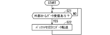
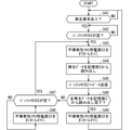
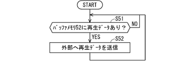
- FIG. It is a flowchart of the data reception processing of the data recorder of Embodiment 1. It is a flowchart of the storage process of the data recorder of Embodiment 1. It is a flowchart of the reproduction data reading process of the data recorder of Embodiment 1. It is a flowchart of the reproduction processing of the data recorder of Embodiment 1.
- FIG. It is a figure for demonstrating operation of the data recorder of Embodiment 2.
- FIG. It is a figure for demonstrating operation of the data recorder of Embodiment 2.
- FIG. 1 is a block diagram showing a configuration of a data recorder 1 which is a data recorder according to the first embodiment.
- the data recorder 1 includes an input interface 2, a storage unit 3, a control unit 4, and an output interface 5.
- the input interface 2 includes a data transmission / reception unit 21 and a buffer memory 22 (first buffer memory).
- the input interface 2 receives data transmitted from the outside of the data recorder 1 and transfers the data to the storage unit 3.
- the input interface 2 temporarily stores the data received from the outside in the buffer memory 22. By temporarily storing the data received from the outside in the buffer memory 22, there is a grace period for turning off the power supply 33 for the non-volatile memory provided in the storage unit 3 as described later.
- the storage unit 3 includes a data transmission / reception unit 31, a non-volatile memory 32, a power supply 33 for the non-volatile memory, and a power supply control signal reception unit 34.
- the data transmission / reception unit 31 receives the data transferred from the input interface 2 and stores it in the non-volatile memory 32. Further, when the data is reproduced, the data is read from the non-volatile memory 32 and the data is transferred to the output interface 5.
- the non-volatile memory 32 is a non-volatile semiconductor memory such as a flash memory, an MRAM, or an EEPROM.
- the power supply 33 for the non-volatile memory is a power supply that supplies power to the non-volatile memory 32, and is switched on and off by the control signal of the power supply transferred from the power supply control signal receiving unit 34.
- the power supply control signal receiving unit 34 receives the power supply control signal transmitted from the control unit 4, and transfers the received power supply control signal to the power supply 33 for the non-volatile memory. In this way, the control unit 4 controls the on / off of the non-volatile memory power supply 33 via the power supply control signal receiving unit 34.
- the control unit 4 includes a command receiving unit 41, a data amount monitoring unit 42, and a power supply control signal transmitting unit 43.
- the command receiving unit 41 receives a command indicating the start of communication.
- the command includes information on whether the communication is recording or playback.
- the command is a command instructing reproduction, the command also includes, for example, information specifying data to be reproduced.
- the data amount monitoring unit 42 monitors the amount of data stored in the buffer memory 22 included in the input interface 2 and the buffer memory 52 included in the output interface 5.
- the power supply control signal transmission unit 43 transmits a power supply control signal to the power supply control signal reception unit 34 included in the storage unit 3.
- the control unit 4 monitors the amount of data stored in the buffer memory 22 by the data amount monitoring unit 42, and when the threshold value (first threshold value, hereinafter referred to as the threshold value 400) is exceeded, the power supply control signal transmission unit 43 A power supply control signal instructing the power supply 33 for the non-volatile memory to be turned on is transmitted to the power supply control signal receiving unit 34.
- the threshold value 400 is predetermined and stored in the control unit 4.
- the method for determining the threshold value 400 is not limited, but may be, for example, the ratio of the amount of data stored in the buffer memory 22 to the capacity of the buffer memory 22 (for example, 80%). Further, even if it is set based on the write speed to the buffer memory 22 and the time required for the non-volatile memory power supply 33 to be writable when the non-volatile memory power supply 33 is switched from off to on. good.
- the output interface 5 has the same structure as the input interface 2, and the output interface 5 includes a data transmission / reception unit 51 and a buffer memory 52 (second buffer memory).
- the output interface 5 has a function of receiving data from the storage unit 3 and transmitting the data to the outside of the data recorder 1.
- the buffer memories 22 and 52 include non-volatile or volatile semiconductor memories such as RAM (Random Access Memory), flash memory, MRAM, and EEPROM, magnetic disks, flexible disks, optical disks, compact disks, mini disks, and DVDs. Etc., any of the rewritable memories, or a combination thereof.
- the buffer memories 22 and 52 may have a smaller storage capacity than the non-volatile memory 32, and may be configured to be less susceptible to the adverse effects of radiation as compared with the non-volatile memory 32, or may be a package including a plurality of memory modules. With a certain configuration, etc., it is easy to suppress the influence when a partial failure occurs due to the adverse effect of radiation.
- the adverse effect of radiation on a semiconductor device is called a single event effect (SEE).
- the main examples of the single event effect are a single event upset (hereinafter referred to as an upset) in which the data stored by radiation is rewritten, and a single event latch-up in which an overcurrent flows. , SEL, hereinafter referred to as latch-up).
- a CMOS IC Complementary metal-axis-semiconductor Integrated Circuit
- the CMOS IC is exposed to radiation and latches up, it becomes uncontrollable. The current may continue to flow and destroy the circuit.
- As a countermeasure against latch-up by turning off the power of the data recorder 1 or its component, it is possible to prevent the occurrence of latch-up in the data recorder 1 or its component.
- FIG. 2 is a flowchart of the data reception process of the data recorder 1.
- the input interface 2 attempts to receive the data transmitted from the outside of the data recorder 1 (step S21), and if the data is received from the outside (step S21: YES), the input interface 2 sequentially receives the data.
- the transferred data is transferred to the buffer memory 22, and the transferred data is erased (step S22). If the data is not received from the outside in step S21 (step S21: NO), the attempt to receive the data transmitted from the outside is repeated in step S21. Further, after step S22, the process proceeds to step S21 again.
- FIG. 3 shows a flowchart of the storage process of the data recorder 1.
- the control unit 4 monitors the amount of data stored in the buffer memory 22 by the data amount monitoring unit 42, and determines whether or not the threshold value 400 has been exceeded (step S31). When the amount of data stored in the buffer memory 22 exceeds the threshold value 400 (step S31: YES), the control unit 4 sends the power supply control signal to the power supply control signal receiving unit 34 by the power supply control signal transmitting unit 43, and is non-volatile. The power supply of the power source 33 for sex memory is switched from the off state to the on (step S32).
- the data transmission / reception unit 21 reads the data from the buffer memory 22 and transfers the data to the storage unit 3 (step S33). ). The data transferred to the storage unit 3 is written in the non-volatile memory 32.
- the data amount monitoring unit 42 monitors the amount of data stored in the buffer memory 22 again, and determines whether or not the buffer memory 22 is empty (step S34). If the buffer memory 22 is not empty in step S34 (step S34: NO), that is, if the data stored in the buffer memory 22 remains, the process proceeds to step S33, and the data transfer to the storage unit 3 is repeated. ..
- step S34 If all the data in the buffer memory 22 is transferred and the buffer memory 22 is empty (step S34: YES), the control unit 4 transmits a power control signal to the power control signal receiving unit 34 by the power control signal transmitting unit 43. The power supply of the non-volatile memory power supply 33 is switched off (step S35).
- the data recorder 1 receives data from the outside and stores it in the non-volatile memory 32 by the data reception process and the storage process described above. At that time, the control unit 4 turns on the power supply 33 for the non-volatile memory at a timing determined based on the amount of data recorded in the buffer memory 22, as in steps S31 and S32 of the flowchart of FIG.
- the switching and input interface 2 transfers the data recorded in the non-volatile memory 22 to the non-volatile memory 32 when the power supply 33 for the non-volatile memory is on, and the control unit 4 is recorded in the buffer memory 22. After the transfer of the data to the non-volatile memory 32 is completed, the power supply 33 for the non-volatile memory is switched off.
- the adverse effects of radiation can be suppressed, and the power consumption of the data recorder 1 can be reduced.
- the adverse effect of radiation can be suppressed by turning off the non-volatile memory 32.
- the data recorder 1 can be power-saving.
- FIG. 4 is a flowchart of the reproduction data reading process.
- the reproduction data reading process is a process of reading the reproduction data from the non-volatile memory 32 to the buffer memory 52 for the reproduction process described later. Further, the reproduction data is the data to be output of the data recorder 1, that is, the data to be reproduced, and is, for example, the data designated to be reproduced by the reproduction request command received by the command receiving unit 41.
- step S41 The control unit 4 confirms whether the command receiving unit 41 has received the playback request command (step S41). If there is a reproduction request command received by the command receiving unit 41 (step S41: YES), the process proceeds to step S42. If there is no playback request command received by the command receiving unit 41 (step S41: NO), step S41 is repeated.
- step S42 it is confirmed whether the buffer memory 52 is empty (step S42). If the buffer memory 52 is not empty (step S42: NO), step S42 is repeated until the reproduction of the data remaining in the buffer memory 52 is completed and the buffer memory 52 becomes empty.
- step S42 If the buffer memory 52 is empty (step S42: YES), the control unit 4 transmits a power supply control signal to the power supply control signal receiving unit 34 by the power supply control signal transmitting unit 43, and turns off the power supply of the non-volatile memory power supply 33. To switch on (step S43).
- the data transmission / reception unit 31 included in the storage unit 3 reads the reproduced data from the non-volatile memory 32 of the storage unit 3 and transmits the reproduction data to the data transmission / reception unit 51 provided in the output interface 5 (step S44).
- the data transmission / reception unit 51 writes the reproduction data received from the data transmission / reception unit 31 to the buffer memory 52 (step S45).
- steps S44 and S45 when the amount of regenerated data that has not yet been read from the non-volatile memory 32 is larger than the capacity of the non-volatile memory 32, the regenerated data that can be stored in the non-volatile memory 32 is the non-volatile memory 32. Is read from and transmitted to the buffer memory 52 via the data transmission / reception unit 31 and the data transmission / reception unit 51.
- control unit 4 determines whether all the reproduced data has been read from the non-volatile memory 32 of the storage unit 3 and transmitted to the buffer memory 52 (step S46).
- step S46 If the reading of some of the reproduced data from the non-volatile memory 32 and the transmission to the buffer memory 52 have not been completed (step S46: NO), the process proceeds to step S47.
- step S47 the control unit 4 confirms whether the buffer memory 52 is empty (step S47).
- step S47 NO
- the control unit 4 turns off the power supply 33 for the non-volatile memory (step S48) until the buffer memory 52 becomes empty by the reproduction process described later.
- step S47 is repeated.
- the control unit 4 is switched off by the power control signal transmission unit 43 when the non-volatile memory power supply 33 is originally on, and is turned off when the non-volatile memory power supply 33 is originally off. Leave it as it is.
- step S47 If the buffer memory 52 is empty in step S47 (step S47: YES), the process proceeds to step S43.
- step S46 when all the reproduced data has been read from the non-volatile memory 32 and transmitted to the buffer memory 52 (step S46: YES), the control unit 4 is used for the non-volatile memory by the power supply control signal transmission unit 43.
- the power supply of the power supply 33 is switched from on to off (step S49), and the process proceeds to step S41.
- FIG. 5 is a flowchart of the reproduction process.
- the reproduction process is a process of transmitting the reproduction data read from the non-volatile memory 32 and transmitted to the buffer memory 52 in the reproduction data reading process to the outside via the output interface 5.
- the data transmission / reception unit 51 determines whether or not there is reproduction data in the buffer memory 52 (step S51), and if there is reproduction data in the buffer memory 52 (step S51: YES), the reproduction data in the buffer memory 52 is used. It is transmitted to the outside, and the reproduced data that has been transmitted is erased from the buffer memory 52 (step S52). After step S52, step S51 is repeated.
- step S51 If there is no reproduction data in the buffer memory 52 in step S51 (step S51: NO), step S51 is repeated.
- the data recorder 1 saves the reproduction data stored in the non-volatile memory 32 via the buffer memory 52, that is, once stored in the buffer memory 52 by the reproduction data reading process and the reproduction process described above, and then from the buffer memory 52. Read and output to the outside.
- the control unit 4 has a grace period to turn off the power supply 33 for the non-volatile memory during data reproduction, the control unit 4 starts transferring the reproduced data to the buffer memory 52 in step S48 of the flowchart of FIG.
- the power supply 33 for the non-volatile memory is turned off during a part of the period from the start to the transfer of the reproduced data to the buffer memory 52.
- the control unit 4 powers the non-volatile memory power supply 33 during a part of the period from the start of transfer of the reproduction data to the buffer memory 52 to the end of the transfer of the reproduction data to the buffer memory 52. Turn it off. As a result, the adverse effects of radiation can be suppressed.
- the data recorder 1 is used for the non-volatile memory while executing data input from the outside, instead of controlling the on / off of the power supply 33 for the non-volatile memory in steps S32 and S35.
- the configuration may be such that the power supply 33 is turned on and the power supply 33 for the non-volatile memory is turned off except when data input from the outside is being executed. Even in the data recorder 1 having such a configuration, ⁇ A-3. Effect> The effect described in is obtained.
- step S42 and step S47 the control unit 4 determines whether or not the buffer memory 52 is empty, but instead of determining whether or not the buffer memory 52 is empty, the amount of data stored in the buffer memory 52 is a threshold value ( It may be determined whether or not the value is less than the second threshold value (hereinafter referred to as the threshold value 401).
- the threshold value 401 is, for example, a range in which the buffer memory 52 is not emptied before the non-volatile memory power supply 33 is switched on and reading from the non-volatile memory 32 becomes possible in consideration of the rise time of the non-volatile memory 32. Therefore, it is set as a value as small as possible and stored in the control unit 4.
- the control unit 4 turns off the power supply 33 for the non-volatile memory during a part of the period until the reproduction data is completely transferred to the buffer memory 52.
- the control unit 4 turns off the power supply 33 for the non-volatile memory during a part of the period until the reproduction data is completely transferred to the buffer memory 52.
- steps S42 and S47 if the amount of reproduced data that has not yet been read from the non-volatile memory 32 is equal to or less than the free capacity of the buffer memory 52, the process proceeds to step S43 and the data has not been read yet.
- the reproduction data may be transferred to the buffer memory 52.
- control unit 4 writes to the non-volatile memory 32 and / or writes to the non-volatile memory 32 so that the writing to the non-volatile memory 32 and / or reading from the non-volatile memory 32 during execution is not hindered.
- the power supply 33 for the non-volatile memory is switched off only at the timing when the reading from is not performed.
- step S35 of the flowchart of the storage process shown in FIG. 3 control is performed at the timing when writing to the non-volatile memory 32 and / or reading from the non-volatile memory 32 is performed in a process other than the storage process.
- the unit 4 does not switch off the power supply 33 for the non-volatile memory, and proceeds to step S31.
- the timing at which writing to the non-volatile memory 32 and / or reading from the non-volatile memory 32 in a process other than the storage process is performed is, for example, step S44 of the flowchart of the reproduction data read process shown in FIG. It is the timing when the processing of is being performed.
- step S35 at the timing when the writing to the non-volatile memory 32 and the reading from the non-volatile memory 32 are not performed in the processing other than the storage processing, ⁇ A-2.
- the control unit 4 switches off the power supply 33 for the non-volatile memory and proceeds to step S31.
- the control unit 4 turns off the power supply 33 for the non-volatile memory even at the timing when writing to the non-volatile memory 32 and / or reading from the non-volatile memory 32 is performed in a predetermined situation, and the control unit 4 is determined in advance.
- the power supply 33 for the non-volatile memory may be turned off only at the timing when the writing to the non-volatile memory 32 and the reading from the non-volatile memory 32 are not performed.
- the predetermined situation is, for example, a situation in which a command for forcibly turning off the power supply 33 for the non-volatile memory is received from the outside via the command receiving unit 41.
- the predetermined situation is determined. For example, when the overcurrent of the non-volatile memory power supply 33 is detected, the non-volatile memory power supply 33 is turned off.
- Embodiment 2 In the data recorder 1 of the first embodiment, when the amount of data stored in the buffer memory 22 provided in the input interface 2 exceeds the threshold value, the power supply 33 for the non-volatile memory is changed from off to on.
- the threshold value 400 used in the first embodiment as the threshold value of the amount of data stored in the buffer memory 22 is a fixed value and does not fluctuate. However, when the communication speed at which the data recorder receives or transmits data from the outside is not constant, it is desirable to be able to dynamically change the threshold value from the viewpoint of radiation countermeasures and power saving.
- FIG. 6 is a block diagram showing a configuration of a data recorder 1b, which is a data recorder according to the second embodiment.
- the data recorder 1b is different from the data recorder 1 which is the data recorder according to the first embodiment in that the control unit 4 is the control unit 4b.
- the input interface 2 and the output interface 5 are limited to be able to communicate with the outside at a plurality of communication speeds, but will be described as the input interface 2 and the output interface 5 which are the same interfaces as the first embodiment. ..
- the configuration of the data recorder 1b is the same as that of the data recorder 1b.
- the communication speed with the outside is the speed of data input when data is input to the data recorder 1b from the outside, and the speed of data output when data is output from the data recorder 1b to the outside.
- the data recorder 1b may not only be able to communicate with the outside at a plurality of communication speeds, but may also have a configuration in which the communication speed differs between the input and the output.
- the control unit 4b further includes a threshold control unit 44 as compared with the control unit 4. Similar to the control unit 4 of the first embodiment, the control unit 4b monitors the amount of data stored in the buffer memory 22 by the data amount monitoring unit 42, and when the threshold value 400 is exceeded, the power supply control signal transmission unit 43 transmits a power supply control signal instructing the power supply control signal receiving unit 34 to turn on the power supply 33 for the non-volatile memory. In the present embodiment, the threshold control unit 44 controls the threshold value 400.
- the command indicating the start of communication received by the command receiving unit 41 included in the control unit 4b includes information on the communication speed. Other than that, the configuration of the control unit 4b is the same as that of the control unit 4.
- the communication with low communication speed is defined as low-speed data communication, and the other is defined as high-speed data communication.
- the threshold value 400 is set to be suitable for low-speed data communication, that is, the buffer memory 22 does not overflow and the buffer memory 22 can be fully utilized in the case of low-speed data communication, the threshold value 400 of the same value is used.
- the buffer memory 22 may overflow.
- the threshold value 400 is set to be suitable for high-speed data communication, that is, the buffer memory 22 does not overflow and the buffer memory 22 can be fully utilized in the case of high-speed data communication, the threshold value 400 of the same value is set.
- the buffer memory 22 has free space, that is, the power supply 33 for the non-volatile memory is turned on while there is a grace period for keeping the power supply 33 for the non-volatile memory turned off. Will switch to. That is, there is room to extend the time in which the non-volatile memory power supply 33 is off, and there is room for more effective radiation countermeasures and power saving.
- the storage capacity of the buffer memory 22 is defined as MB [Gbit], and the amount of data stored in the buffer memory 22 is defined as MW [Gbit].
- the rise time of the non-volatile memory 32 is T POW [s]
- the communication speed of the input from the outside is A [Gbps].
- the communication speed A is either the communication speed A0 in high-speed data communication or the communication speed A1 in low-speed data communication, but it is considered that the communication speed A is fixed to either one in a series of communication.
- a 0 and A 1 satisfy A 0 > A 1 .
- TOVR (MB ⁇ MW ) / A.
- MLIM MB ⁇ A ⁇ T POW .
- MB 5 Gbit
- a 0 2 Gbps
- a 1 1 Gbps
- T POW 1s
- the data transfer speed from the buffer memory 22 to the non-volatile memory 32 is the data input from the outside.
- the values given here are examples and can be changed according to the design of the data recorder 1b.
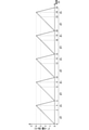
- FIG. 7 shows the variation of MW when the threshold value 400 is M 0 LIM .
- FIG. 8 shows the variation of MW when the threshold value 400 is M 1 LIM .
- the time during which the non-volatile memory power supply 33 is on can be reduced by setting the threshold value 400 to a larger value.
- the threshold value 400 is M 1 LIM
- the buffer memory 22 can be used effectively as compared with the case where the threshold value 400 is M 0 LIM , so that the number of times of switching the power supply 33 for the non-volatile memory 33 can be reduced. You can reduce the amount of time you are on. In the example of FIG. 7, the time that the non-volatile memory power supply 33 is on due to the rise time of the non-volatile memory 32 is 5 seconds out of 25 seconds, but in the example of FIG.
- the non-volatile memory power supply 33 is turned on. Since the number of switchings between and off is reduced, the time that the power supply 33 for the non-volatile memory is on due to the rise time of the non-volatile memory 32 is 4 seconds out of 25 seconds.
- the threshold value of the maximum value is M 0 LIM for high-speed data communication and M 0 LIM for low-speed data communication within the range where the non-volatile memory 32 does not overflow so as not to interfere with data input from the outside. Is M 1 LIM and is different. Therefore, in the data recorder 1b of the present embodiment, the threshold control unit 44 sets the threshold value 400 to M 0 LIM in the case of high-speed data communication and M 0 LIM in the case of low-speed data communication based on the speed of data input from the outside.
- the threshold 400 is set to M 1 LIM .
- the threshold value 400 is set slightly smaller than M 0 LIM or M 1 LIM in consideration of the fluctuation.
- the control unit 4b is based on the amount of data recorded in the buffer memory 22 and the speed of data input from the outside via the input interface 2.
- the power supply 33 for the non-volatile memory is switched on.
- the threshold control unit 44 included in the control unit 4b determines the threshold value 400 based on the speed of data input from the outside, and the control unit 4b is shown in steps S31 and S32 of the flowchart of FIG.
- the power supply 33 for the non-volatile memory is switched on.
- the input interface 2 transfers the data recorded in the non-volatile memory 22 to the non-volatile memory 32 when the power supply 33 for the non-volatile memory is on, and the control unit 4 records the data in the buffer memory 22. After transferring the data to the non-volatile memory 32, the power supply 33 for the non-volatile memory is switched off. With such a configuration, since the time that the non-volatile memory power supply 33 is in the ON state is reduced, the adverse effect of radiation can be further suppressed, and the data recorder 1b can be further reduced in power consumption.
- the adverse effect of radiation can be further suppressed, and the adverse effect of radiation can be further suppressed.
- the data recorder 1b can be further reduced in power consumption.
- the threshold control unit 44 when the power supply 33 for non-volatile memory is turned off from on, it is assumed that the writing to the power supply 33 for non-volatile memory can be turned off instantly after the writing is completed. If it takes time for the power supply 33 for non-volatile memory to turn off after writing to the power supply 33 for non-volatile memory is completed, the threshold control unit 44 also bases the time for that amount on the speed of data input from the outside. By switching the non-volatile memory power supply 33 on at the predetermined timing, it can be reduced as the number of times the non-volatile memory power supply 33 is switched on and off decreases.
- FIGS. 7 and 8 have been described assuming a situation where the data input speed is constant during a series of data input, the data input speed may change during the series of data input.
- the control unit 4b is recorded in the buffer memory 22.
- the change in the data input speed is permitted after the amount of the existing data becomes the threshold value of 400 or less, which is determined based on the changed data input speed.
- the threshold control unit 44 uses the speed of data input from the outside as a command from the outside received by the command receiving unit 41. It can also be obtained by monitoring the information on the included communication speed, the information on the operating status of the data transmission / reception unit 21, and the fluctuation speed of the amount of data stored in the buffer memory 22, and even in these cases, it is practically possible. In addition, it can be said that the threshold control unit 44 controls the threshold 400 based on the speed of data input.
- the control unit 4b turns on the power supply 33 for the non-volatile memory at a timing determined based on the amount of data recorded in the buffer memory 22 and the speed of data input from the outside via the input interface 2. Although described as switching, more generally, it may be based on the mode of data entry rather than the speed of data entry. For example, if it is known from the command received by the command receiving unit 41 that the data is input intermittently at intervals of a certain amount or less, for example, the free space is fixed based on the fixed amount.
- the threshold value 400 may be controlled so that the data is transferred to the non-volatile memory 32 when the amount is less than or equal to the amount.
- the control unit 4b is for the non-volatile memory at a timing determined based on the amount of data recorded in the buffer memory 22 and the speed of data input from the outside via the input interface 2.
- the power supply 33 is switched on, the input interface 2 transfers the data recorded in the buffer memory 22 to the non-volatile memory 32 when the power supply 33 for the non-volatile memory is on, and the control unit 4 transfers the buffer.
- the non-volatile memory power supply 33 is switched off. As a result, the adverse effects of radiation can be suppressed.
- the control unit 4b is, for example, ⁇ A-5.
- the threshold value 401 described in the modification 2> is controlled based on the mode of data output to the outside.
- the threshold control unit 44 sets, for example, the smallest possible threshold value in the threshold value so that the buffer memory 52 does not become empty before the data can be read from the non-volatile memory 32 after step S43, and the mode of data output during execution. For example, it is set according to the speed of data output.
- it is possible to prevent the data output from being hindered by controlling the on / off of the power supply 33 for the non-volatile memory, and to suppress the time during which the power supply 33 for the non-volatile memory is on, which is adversely affected by radiation.
- the power saving of the data recorder 1 can be achieved. In particular, when data reproduction continues for a long time and an amount of data equal to or larger than the capacity of the buffer memory 52 is reproduced, adverse effects due to radiation can be suppressed, and power saving of the data recorder 1 can be achieved.
- the non-volatile memory power supply 33 is turned off when it is not necessary to turn it on, thereby suppressing the frequency of latch-up caused by radiation, for example.
- the data recorder 1c which is the data recorder according to the third embodiment, the current value of the non-volatile memory power supply 33 is monitored as a countermeasure against the occurrence of latch-up, and when an overcurrent is detected, the non-volatile memory power supply 33 is detected. Power is switched off.
- FIG. 9 is a block diagram showing the configuration of the data recorder 1c.
- the data recorder 1c is different from the data recorder 1 which is the data recorder according to the first embodiment in that the control unit 4 is the control unit 4c. Other than that, the configuration of the data recorder 1c is the same as that of the data recorder 1c.
- the control unit 4c further includes a current value monitoring unit 45 as compared with the control unit 4.
- the current value monitoring unit 45 acquires and monitors the current value of the non-volatile memory power supply 33.
- the current value monitoring unit 45 acquires the current value of the non-volatile memory power supply 33 from, for example, an ammeter provided in the non-volatile memory power supply 33.
- a current threshold value (third threshold value, hereinafter, current threshold value 60), which is a safe current value in terms of specifications of the non-volatile memory 32 and the non-volatile memory power supply 33, is recorded in advance. Further, the control unit 4c is described in ⁇ C-2. The process for detecting latch-up and preventing failure or suppressing the frequency of failure, as described in Operation>, is performed.
- the control unit 4c has the same configuration as the control unit 4 except that the control unit 4c has the same configuration as the control unit 4.
- the control unit 4c is further provided with the current value monitoring unit 45 as compared with the control unit 4, but the control unit 4c is further provided with the current value monitoring unit 45 as compared with the control unit 4b, and the data recorder 1c is ⁇ B-2.
- the same operation as the operation> may be performed.
- the data recorder 1c is the same as the data recorder 1 ⁇ A-2. Operation> is performed. However, ⁇ A-2. In the description of operation>, the control unit 4 is read as the control unit 4c.
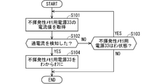
- FIG. 10 is a flowchart showing a process for the data recorder 1c to detect latch-up and prevent a failure or suppress the frequency of failures.
- the current value monitoring unit 45 acquires the value of the current flowing through the non-volatile memory power supply 33 when the power of the non-volatile memory power supply 33 is turned on (step S101).
- the value of the current flowing through the non-volatile memory power supply 33 measured by the current value monitoring unit 45 is hereinafter referred to as a measured current value.
- the current value monitoring unit 45 determines whether the measured current value exceeds the current threshold value 60 (step S102). If the measured current value does not exceed the current threshold value 60, that is, if no overcurrent is detected (step S102: NO), the process proceeds to step S103.
- step S103 the control unit 4c confirms whether the state of the non-volatile memory power supply 33 is on, and if the non-volatile memory power supply 33 is in the off state (step S103: NO), it is shown in FIG. Ends the operation of the flow chart. If the non-volatile memory power supply 33 is in the ON state in step S103 (step S103: YES), the process proceeds to step S101.
- the current value monitoring unit 45 sets the current threshold value 60 for the value of the current flowing through the non-volatile memory power supply 33 while the non-volatile memory power supply 33 is on. Continue to monitor for excess.
- step S102 when the current value monitoring unit 45 determines that the measured current value exceeds the current threshold value 60, that is, when an overcurrent is detected (step S102: YES), the control unit 4c is the power supply control signal transmission unit.
- the power supply 33 for the non-volatile memory is switched off by 43 (step S104).
- the non-volatile memory power supply 33 includes a plurality of power supply devices and the plurality of power supply devices each supply power to the non-volatile memory 32, only the power supply device in which an abnormality is detected is switched off. May be good.
- step S104 When the non-volatile memory power supply 33 is turned off in step S104, the operation of the flowchart shown in FIG. 10 ends.
- control unit 4c switches off the power supply of the non-volatile memory power supply 33 at the timing determined by the current value monitoring unit 45 based on the measured current value. Specifically, when the measured current value exceeds the current threshold value 60, the power supply of the non-volatile memory power supply 33 is switched off. As a result, it is possible to detect the occurrence of latch-up that may occur when the non-volatile memory power supply 33 is on, and prevent the data recorder 1c from failing due to the latch-up or suppress the frequency of failures.
- the control unit 4c includes a current value monitoring unit 45, and the control unit 4c turns off the power supply of the non-volatile memory power supply 33 at a timing determined by the current value monitoring unit 45 based on the measured current value. Switch.
- the data recorder 1c can detect the occurrence of latch-up and prevent the data recorder 1c from failing due to the latch-up or suppress the frequency of failures.
- Embodiment 4 The data recorder 1, the data recorder 1b, and the data recorder 1c described in the first to third embodiments suppress the occurrence of upset and latch-up by switching the power supply 33 for the non-volatile memory on and off. Was.
- the data recorder 1d which is the data recorder according to the present embodiment, suppresses the occurrence of uncorrectable soft errors by reading the data and writing back the corrected data.
- FIG. 11 is a block diagram showing the configuration of the data recorder 1d.
- the lines representing the operations of the command receiving unit 41, the data amount monitoring unit 42, and the power supply control signal transmitting unit 43 are omitted.
- the data recorder 1d is different from the data recorder 1 which is the data recorder according to the first embodiment in that the storage unit 3 is the storage unit 3d and the control unit 4 is the control unit 4d. Other than that, the configuration of the data recorder 1d is the same as that of the data recorder 1d.
- the non-volatile memory 32 is a non-volatile memory 32d as compared with the storage unit 3. In other respects, the storage unit 3d is the same as the storage unit 3.
- the non-volatile memory 32d When storing the data, the non-volatile memory 32d also stores the error correction code of the data.
- the error correction code may be stored in a memory other than the non-volatile memory 32. Further, the error correction code may be of any format as long as the error of the data stored in the non-volatile memory 32 can be corrected.
- the control unit 4d further includes a storage data update unit 46 as compared with the control unit 4.
- the storage data update unit 46 is described in ⁇ D-2. Perform the storage data update process described in Operation>. Other than that, the configuration of the control unit 4d is the same as that of the control unit 4.
- control unit 4d has been described as further including a storage data update unit 46 as compared with the control unit 4, the control unit 4d may further include a current value monitoring unit 45 as compared with the control unit 4b or the control unit 4c.
- data recorder 1d is ⁇ B-2. Operation> or ⁇ C-2. Operation> or both may be performed in the same manner.
- the data recorder 1d is the same as the data recorder 1 ⁇ A-2. Operation> is performed. However, ⁇ A-2.
- the storage unit 3 is read as a storage unit 3d
- the non-volatile memory 32 is read as a non-volatile memory 32d
- the control unit 4 is read as a control unit 4d.
- the storage data update unit 46 determines whether or not there is a margin for reading data from the non-volatile memory 32 based on the access status of writing and reading to the non-volatile memory 32, and the non-volatile memory 32 has a margin for reading. Occasionally, the stored data, which is the data stored in the non-volatile memory 32, is read from the non-volatile memory 32. At this time, the error correction code of the stored data is also acquired, and the presence or absence of a soft error in the stored data is determined. If no soft error is detected, it is not necessary to write back to the non-volatile memory 32. When a soft error is detected, the data corrected by the soft error is written back to the non-volatile memory 32 when there is a margin for writing in the access status of the non-volatile memory 32.
- the data stored in the non-volatile memory 32 is read from the non-volatile memory 32, and if a soft error occurs, the data after the soft error correction is written back to the non-volatile memory 32.
- the storage data update process it is possible to prevent or suppress the frequency of soft errors that exceed the correction capability of the error correction code and prevent the errors from being corrected in the stored data of the non-volatile memory 32, and the non-volatile memory is non-volatile.
- the reliability of the data stored in the sex memory 32 can be improved.
- the determination of whether or not there is a margin for reading data or writing data for example, it can be determined that there is a margin when the power supply 33 for the non-volatile memory is off. However, it may be determined whether or not the data can be read or the data can be written by another method. Further, in order to allow the non-volatile memory 32 to have a margin for reading or writing data, the data transfer rate between the buffer memory 22 or the buffer memory 52 and the non-volatile memory 32 may be lowered.
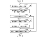
- the operation procedure of the stored data updating unit 46 in the data recorder 1d according to the fourth embodiment described above will be described according to the flowchart shown in FIG.
- the operation of the storage data updating unit 46 starts the operation of the flowchart shown in FIG. 12, for example, periodically or by a command via the user's command receiving unit 41.
- the storage data update unit 46 first confirms whether the non-volatile memory 32 has a margin for reading, that is, whether it can be read (step S121). If it is not readable (step S121: NO), step S121 is repeated, and the confirmation work is continued until readable.
- the storage data update unit 46 reads the storage data of a predetermined size from the non-volatile memory 32, and corrects the error in the read storage data.
- the code is also acquired (step S122).
- the predetermined size may be an arbitrarily set size.
- the control unit 4e turns on the non-volatile memory power supply 33 by the power control signal transmission unit 43, and then the storage data update unit 46 is non-volatile. Read data from the non-volatile memory 32.
- the storage data update unit 46 determines the presence or absence of a soft error based on the read storage data and the acquired error correction code (step S123). As a result, if no soft error is detected (step S123: NO), it is not necessary to rewrite the data read in step S122 to the non-volatile memory 32, so the process proceeds to step S126.
- step S123 If a soft error is detected in step S123 (step S123: YES), the read data needs to be written again to the non-volatile memory 32 after the soft error is corrected, so that the storage data update unit 46 performs the non-volatile memory 32. Check if it is writable to (step S124).
- step S124 If it is not writable to the non-volatile memory 32 (step S124: NO), the storage data update unit 46 repeats step S124 until it becomes writable, and continues the confirmation work.
- step S124 When the data can be written to the non-volatile memory 32 (step S124: YES), the storage data update unit 46 writes back the data after the soft error correction to the non-volatile memory 32 (step S125), and after the writing is completed, the data is written back to the non-volatile memory 32. The process proceeds to step S126.
- step S126 the storage data update unit 46 determines whether or not to end the storage data update process. For example, if all the update processing for the data stored in the non-volatile memory 32 at the start of the storage data update processing is completed, the process ends, and if not, the process returns to step S121.
- step S126 when the storage data update process is completed, if the data is not reproduced or recorded, the control unit 4e turns off the power supply 33 for the non-volatile memory by the power supply control signal transmission unit 43, and then the control unit 4e turns off the power supply 33 for the non-volatile memory. The storage data update process is completed.
- the storage data update unit 46 performs the storage data update process.
- the storage data update unit 46 performs the storage data update process.
- Embodiment 5 In the data recorder 1d according to the fourth embodiment, for example, by periodically reading out the stored data, detecting an error, and writing back the corrected data, an error can be obtained even if an error correction code is used. Was prevented from becoming uncorrectable. However, the frequency of soft errors caused by upsets and the like depends on the environment. Therefore, it is desirable that the frequency of reading the data, detecting the error, writing back the error-corrected data, and performing the storage data update process can be dynamically changed.
- the data recorder 1e which is a data recorder according to the present embodiment, monitors the frequency of soft error occurrence and dynamically changes the frequency of the stored data update process to suppress the execution of unnecessary stored data update process. In addition, it suppresses the occurrence of errors that cannot be corrected due to changes in the environment.
- FIG. 13 is a block diagram showing the configuration of the data recorder 1e.
- the lines representing the operations of the command receiving unit 41, the data amount monitoring unit 42, and the power supply control signal transmitting unit 43 are omitted.
- the data recorder 1e includes a control unit 4e instead of the control unit 4d as compared with the data recorder 1d according to the fourth embodiment. Other than that, the configuration of the data recorder 1e is the same as the configuration of the data recorder 1d.
- the control unit 4e further includes a storage data update plan determination unit 47 as compared with the control unit 4d.
- the configuration of the control unit 4e is the same as the configuration of the control unit 4d.
- the storage data update plan determination unit 47 obtains error information regarding the occurrence mode of the soft error obtained in the storage data update process from the storage data update unit 46, for example, the number of detected errors or the number of errors per data amount. get.
- the storage data update plan determination unit 47 determines an update plan, which is a plan for the storage data update process, based on the mode in which a soft error occurs, and the storage data update unit 47 determines the storage data update process based on the update plan. Instruct 46.
- the number of errors that can be corrected for a certain amount of data is usually determined by the format of the error correction code.
- the maximum value of the number of errors that can be corrected for a certain amount of data is Nemax .
- the storage data update plan determination unit 47 specifically determines the plan for the storage data update process by, for example, the following operation.
- the storage data update plan determination unit 47 acquires the number of errors detected in the storage data update process from the storage data update unit 46, and calculates the average value Nave of the number of occurrences per certain amount of data.
- the average value Nave is, for example, the average of the most recent one-time or multiple-time storage data update processing.
- the storage data update plan determination unit 47 determines, for example, a predetermined ratio of the Nave value expected in the next storage data update process to Nemax when it is assumed that the number of errors generated per hour does not change.
- the frequency of storage data update processing should be as low as possible within the range of the following values. As a result, assuming that the environment changes more slowly than the storage data update processing interval, if many soft errors occur, it will occur every time the storage data update processing is performed by increasing the frequency of the storage data update processing. If the expected value of the number of uncorrectable errors is preferably kept below a certain level and soft errors rarely occur, unnecessary storage data update processing can be omitted.
- the predetermined ratio can be arbitrarily set as a design value, but may be specified by the user via the command receiving unit 41.
- the stored data is kept below a certain value so that the expected value of the number of uncorrectable errors that occur per hour is kept below a certain value.
- the frequency of update processing may be determined.
- the storage data update plan determination unit 47 may, for example, use the time interval between the storage data update processes. The maximum value of may be set.
- the minimum value of the time interval between the storage data update processes is set. And so on.
- the stored data update plan determination unit 47 determines a plan for the stored data update process based on the mode of occurrence of the soft error detected in the stored data update process. As a result, the reliability of the data stored in the non-volatile memory 32 can be improved, and the time during which the non-volatile memory power supply 33 is on can be suppressed, for example, the occurrence of latch-up can be suppressed.
- Embodiment 6 In the present embodiment, the hardware configuration of the data recorders 1 to the data recorders 1e described in the first to fifth embodiments will be described.
- FIG. 14 is a diagram showing the hardware configurations of the data transmission / reception unit 21, the data transmission / reception unit 31, the data transmission / reception unit 51, the power supply control signal reception unit 34, and the control units 4, 4b, 4c, 4d, 4e.
- the buffer memories 22, 52, the non-volatile memory 32, the non-volatile memory power supply 33, and the like are not shown.
- Each function of the data transmission / reception unit 21, the data transmission / reception unit 31, the data transmission / reception unit 51, the power supply control signal reception unit 34, and the control units 4, 4b, 4c, 4d, 4e is realized by the processing circuit HW1.
- Each function of the update unit 46 and the storage data update plan determination unit 47 is realized by the processing circuit HW1.
- the processing circuit HW1 may be dedicated hardware or a CPU (central processing unit) that executes a program stored in the memory HW2.
- the processing circuit HW1 may be, for example, a single circuit, a composite circuit, a programmed processor, a parallel programmed processor, an ASIC (Application Specific Integrated Circuit), or an FPGA (Field-Programmable). Gate Array) or a combination of these is applicable.
- the functions of the data transmission / reception unit 21, the data transmission / reception unit 31, the data transmission / reception unit 51, the power supply control signal reception unit 34, and the control units 4, 4b, 4c, 4d, and 4e are software and firmware. , Or a combination of software and firmware. Software and firmware are described as programs and stored in the memory HW2.
- the processing circuit HW1 reads and executes the program stored in the memory HW2 to read and execute the data transmission / reception unit 21, the data transmission / reception unit 31, the data transmission / reception unit 51, the power supply control signal reception unit 34, and the control units 4, 4b, 4c. , 4d, 4e functions are realized.
- the functions of the data transmission / reception unit 21, the data transmission / reception unit 31, the data transmission / reception unit 51, the power supply control signal reception unit 34, and the control units 4, 4b, 4c, 4d, and 4e are partially realized by dedicated hardware. The rest may be implemented in software or firmware.
- the memory HW2 is, for example, a non-volatile semiconductor memory such as a flash memory, an MRAM, or an EEPROM, any one of a magnetic disk, a flexible disk, an optical disk, a compact disk, a mini disk, a DVD, or a combination thereof.
- the memory HW2 is, for example, a memory different from the buffer memory 22, the buffer memory 52, and the non-volatile memory 32, but the memory HW2 may be the buffer memory 22 or the non-volatile memory 32.
- FIG. 15 is a data recorder 100 of the present embodiment.
- the data recorder 100 includes an input interface 200, a storage unit 300, and a control unit 4000.
- the storage unit 300 includes a non-volatile memory 32 for storing data and a non-volatile memory power supply 33 which is a power supply for the non-volatile memory 32 and whose on / off control is controlled by the control unit 4000.
- the input interface 200 includes a buffer memory 22 which is a first buffer memory.
- the input interface 200 receives data input from the outside and records it in the buffer memory 22.
- the control unit 4000 turns on the power supply 33 for the non-volatile memory at a timing determined based on the amount of data recorded in the buffer memory 22 and the mode of data input from the outside via the input interface 200.
- the switching and input interface 200 transfers the data recorded in the non-volatile memory 22 to the non-volatile memory 32 when the power supply 33 for the non-volatile memory is on, and the control unit 4000 is recorded in the buffer memory 22. After transferring the data to the non-volatile memory 32, the power supply 33 for the non-volatile memory is switched off. As a result, the data recorder 100 can suppress the adverse effects of radiation.
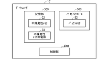
- FIG. 16 is a data recorder 101 of the present embodiment.
- the data recorder 101 includes an output interface 500, a storage unit 300, and a control unit 4001.
- the storage unit 300 includes a non-volatile memory 32 for storing data and a non-volatile memory power supply 33 which is a power supply for the non-volatile memory 32 and whose on / off control is controlled by the control unit 4001.
- the output interface 500 includes a buffer memory 52 which is a second buffer memory.
- the control unit 4001 When the output target data stored in the non-volatile memory 32 is output to the outside via the buffer memory 52, the control unit 4001 starts transferring the output target data to the buffer memory 52 and then outputs the output target.
- the non-volatile memory power supply 33 is turned off during a part of the period until the data is transferred to the buffer memory 52. As a result, the data recorder 101 can suppress the adverse effects of radiation.
- FIG. 17 is a data recorder 102 of the present embodiment.
- the data recorder 102 includes an input interface 200, an output interface 500, a storage unit 300, and a control unit 4002.
- the storage unit 300 includes a non-volatile memory 32 for storing data and a non-volatile memory power supply 33 which is a power supply for the non-volatile memory 32 and whose on / off control is controlled by the control unit 4002.
- the input interface 200 includes a buffer memory 22 which is a first buffer memory.
- the output interface 500 includes a buffer memory 52 which is a second buffer memory.
- the input interface 200 receives data input from the outside and records it in the buffer memory 22.
- the control unit 4002 turns on the power supply 33 for the non-volatile memory at a timing determined based on the amount of data recorded in the buffer memory 22 and the mode of data input from the outside via the input interface 200.
- the switching and input interface 200 transfers the data recorded in the non-volatile memory 22 to the non-volatile memory 32 when the power supply 33 for the non-volatile memory is on, and the control unit 4002 is recorded in the buffer memory 22. After transferring the data to the non-volatile memory 32, the power supply 33 for the non-volatile memory is switched off.
- the data recorder 102 can thereby suppress the adverse effects of radiation.
- the control unit 4002 When the output target data stored in the non-volatile memory 32 is output to the outside via the buffer memory 52, the control unit 4002 starts transferring the output target data to the buffer memory 52 and then outputs the output target.
- the non-volatile memory power supply 33 is turned off during a part of the period until the data is transferred to the buffer memory 52.
- the data recorder 102 can thereby suppress the adverse effects of radiation.
- Embodiment 8> In the present embodiment, how to use the data recorder 1, the data recorder 1b, the data recorder 1c, the data recorder 1d, the data recorder 1e, the data recorder 100, the data recorder 101, and the data recorder 102, respectively, described in the first to sixth embodiments. Will be explained.
- the data recorder 1, the data recorder 1b, the data recorder 1c, the data recorder 1d, the data recorder 1e, the data recorder 100, the data recorder 101, and the data recorder 102 described in the first to fifth embodiments each have a power supply 33 for a non-volatile memory. It is a data recorder with improved radiation resistance by providing a period to turn it off.
- the radiation environment refers to an environment in which the radiation dose is sufficiently higher than the natural environment on the ground, for example, an environment having a radiation dose equivalent to 50 millisieverts or more per year, and the radiation environment is realized in space, for example.
- a radiation environment can be realized on the ground, for example, at a nuclear power plant.
- a data recorder place one of the data recorders in a radiation environment and record the data in either of the data recorders or replay the data recorded in either of the data recorders. This makes it possible to record or reproduce data more stably in a radiation environment. For example, in an observation satellite, a recording request to a data recorder always occurs in a radiation environment, but even in such a case, the data recorder 1 (excluding the configuration of ⁇ A-4.
- Modification 1> and the data recorder.
- the adverse effect of radiation can be suppressed and data can be recorded stably.
Landscapes
- Engineering & Computer Science (AREA)
- Theoretical Computer Science (AREA)
- Physics & Mathematics (AREA)
- General Engineering & Computer Science (AREA)
- General Physics & Mathematics (AREA)
- Quality & Reliability (AREA)
- Techniques For Improving Reliability Of Storages (AREA)
- Memory System (AREA)
Abstract
Description
<A-1.構成>
図1は実施の形態1に係るデータレコーダであるデータレコーダ1の構成を示すブロック図である。
まず、放射線によるデータレコーダ1への悪影響の例について、説明する。放射線による半導体素子への悪影響は、シングルイベント効果(Single Event Effect、SEE)と呼ばれている。シングルイベント効果の主たる例として、放射線によって記憶しているデータが書き換わるシングルイベントアップセット(Single Event Upset、以下、アップセットと記載する)、過電流が流れるシングルイベントラッチアップ(Single Event Latch-up、SEL、以下、ラッチアップと記載する)が挙げられる。例えばデータレコーダ1にCMOS IC(Complementary metal-oxide-semiconductor Integrated Circuit、相補型金属酸化物半導体集積回路)が使われており、CMOS ICに放射線が当たりラッチアップが起これば、制御不能状態となり過電流が流れ続け回路を破壊してしまう可能性がある。ラッチアップへの対策としては、データレコーダ1またはその構成要素の電源をオフとすることにより、データレコーダ1または当該その構成要素でのラッチアップ発生を防止することができる。
図2はデータレコーダ1のデータ受信処理のフローチャートである。
図4は、再生データ読み出し処理のフローチャートである。再生データ読み出し処理は、後述の再生処理のために、再生データを不揮発性メモリ32からバッファメモリ52に読み出す処理のことである。また、再生データは、データレコーダ1の出力対象のデータ、つまり再生しようとするデータであり、例えばコマンド受信部41が受信した再生要求のコマンドで再生するよう指定されたデータのことである。
制御部4は、再生データのバッファメモリ52への転送を開始してから再生データをバッファメモリ52へ転送し終わるまでの間の期間のうちの一部の期間に、不揮発性メモリ用電源33をオフの状態とする。これにより、放射線による悪影響を抑制できる。
上記の<A-2.動作>の項目では、<A-2-1.データ受信処理および記憶処理の動作>において、データレコーダ1へのデータ入力時、制御部4は、バッファメモリ22に記録されているデータの量に基づいて決めたタイミングで、不揮発性メモリ用電源33をオンに切り替え、また、バッファメモリ22に記録されているデータの不揮発性メモリ32への転送が終わった後に、不揮発性メモリ用電源33をオフに切り替えるとして説明した。しかし、データレコーダ1は、図3のフローチャートにおいて、ステップS32およびステップS35の不揮発性メモリ用電源33のオンとオフの制御がなされる代わりに、外部からのデータ入力を実行中は不揮発性メモリ用電源33をオンにし、外部からのデータ入力を実行中以外は不揮発性メモリ用電源33をオフにする、という制御がされる、という構成でもよい。そのような構成のデータレコーダ1においても、<A-3.効果>に記載の効果が得られる。
ステップS42、およびステップS47では、制御部4はバッファメモリ52が空かどうかを判定したが、バッファメモリ52が空かどうかを判定する代わりに、バッファメモリ52の記憶しているデータ量が閾値(第2の閾値、以下、閾値401とする)未満になったかどうか、を判定してもよい。閾値401は、例えば、不揮発性メモリ32の立ち上がり時間を考慮して、不揮発性メモリ用電源33をオンに切り替えて不揮発性メモリ32からの読出しが可能になる前にバッファメモリ52が空にならない範囲で、なるべく小さい値として定められ、制御部4に記憶される。制御部4は、このような構成により、再生データをバッファメモリ52へ転送し終わるまでの間の期間のうちの一部の期間に、不揮発性メモリ用電源33をオフの状態とする。これにより、データレコーダ1へは、外部へのデータ出力に支障をきたすことなく、不揮発性メモリ用電源33をオフの状態の時間を増やし、放射線による悪影響を抑制でき、また、データレコーダ1を省電力化できる。
上記の<A-2.動作>では、記憶処理および再生データ読み出し処理のそれぞれについて、説明中の処理以外では不揮発性メモリ32への書き込みおよび不揮発性メモリ32からの読み出しが行われていない状況を想定して説明をした。しかし、記憶処理または再生データ読み出し処理で不揮発性メモリ用電源33をオフにしようとした際、同時に行われている他の処理において、不揮発性メモリ32への書き込みまたは不揮発性メモリ32からの読み出しまたはその両方が行われている場合も考えられる。そのような場合に、実行中の不揮発性メモリ32への書き込みまたは不揮発性メモリ32からの読み出しまたはその両方が妨げられないよう、制御部4は、不揮発性メモリ32への書き込みおよび不揮発性メモリ32からの読み出しが行われていないタイミングでのみ、不揮発性メモリ用電源33をオフに切り替える。
実施の形態1のデータレコーダ1では、入力インタフェース2の備えるバッファメモリ22に記憶されているデータの量が閾値を超過した場合に、不揮発性メモリ用電源33はオフからオンに変更された。バッファメモリ22に記憶されているデータの量の閾値として実施の形態1で用いた閾値400は固定値であり変動することはない。しかし、データレコーダが外部からのデータを受信、または外部へ送信する通信速度が一定でない場合、放射線対策や省電力化の観点から閾値を動的に変更できることが望ましい。
図6は実施の形態2に係るデータレコーダであるデータレコーダ1bの構成を示すブロック図である。
データレコーダ1bへのデータ入力時のデータレコーダ1bのデータ受信処理および記憶処理の動作はそれぞれ、閾値400が閾値制御部44に制御されるものであることを除けば、実施の形態1の<A-2-1.データ受信処理および記憶処理の動作>で説明した動作と同様である。また、データレコーダ1bのデータ再生時の再生データ読み出し処理および再生処理の動作は、実施の形態1の<A-2-2.再生データ読み出し処理および再生処理の動作>で説明した動作と同様である。但し、実施の形態1の説明の制御部4は制御部4bと読み替える。
データレコーダ1bにおいて、制御部4bは、バッファメモリ22に記録されているデータの量と、入力インタフェース2を介した外部からのデータ入力の速度と、に基づいて決めたタイミングで、不揮発性メモリ用電源33をオンに切り替え、入力インタフェース2は、不揮発性メモリ用電源33がオンの状態の場合に、バッファメモリ22に記録されているデータを不揮発性メモリ32に転送し、制御部4は、バッファメモリ22に記録されているデータを不揮発性メモリ32に転送した後に、不揮発性メモリ用電源33をオフに切り替える。これにより、放射線による悪影響を抑制できる。
実施の形態2では外部からデータレコーダ1bにデータ入力を行う際に不揮発性メモリ用電源33をオンに切り替えるタイミングについて説明した。制御部4bは、データを再生する際に、不揮発性メモリ用電源33をオンに切り替えるタイミングも同様に、バッファメモリ52に記録されているデータの量と、外部へのデータ出力の態様と、に、基づいて、制御してもよい。
上記の<B-2.動作>では、データレコーダ1bのデータ再生時の再生データ読み出し処理および再生処理の動作は、実施の形態1の<A-2-2.再生データ読み出し処理および再生処理の動作>で説明した動作と同様である、として説明した。しかし、データレコーダ1bの制御部4は、再生データのバッファメモリ52への転送を開始してから再生データをバッファメモリ52へ転送し終わるまでの間は、不揮発性メモリ用電源33をオンの状態とし続ける、つまり図4のフローチャートにおいてステップS48の動作を行わない、という構成でもよい。本変形例のデータレコーダ1bによっても、<B-3.効果>に記載の効果が得られる。
実施の形態1および2は不揮発性メモリ用電源33をオンにする必要が無い場合にオフにすることで、例えば放射線起因のラッチアップの頻度を抑制していた。しかし、不揮発性メモリ32が稼働中に放射線起因のラッチアップが起きる可能性はあるため、不揮発性メモリ用電源33がオンの際にラッチアップが発生した場合の対策もあることがより望ましい。実施の形態3に係るデータレコーダであるデータレコーダ1cでは、ラッチアップ発生時の対策のため、不揮発性メモリ用電源33の電流値が監視され、過電流が検知されたら、不揮発性メモリ用電源33の電源がオフに切り替えられる。
図9はデータレコーダ1cの構成を示すブロック図である。
データレコーダ1cはデータレコーダ1と同様、<A-2.動作>の動作を行う。但し、<A-2.動作>の説明において、制御部4は制御部4cと読み替える。
データレコーダ1cにおいて、制御部4cは電流値監視部45を備え、制御部4cは、電流値監視部45が計測電流値に基づいて決めたタイミングで、不揮発性メモリ用電源33の電源をオフに切り替える。これにより、データレコーダ1cは、ラッチアップの発生を検出し、ラッチアップに起因するデータレコーダ1cの故障を防止または故障の頻度を抑制することができる。
実施の形態1から3で説明したデータレコーダ1、データレコーダ1b、およびデータレコーダ1cは、いずれも、不揮発性メモリ用電源33のオンとオフを切替えることで、アップセットやラッチアップの発生を抑制していた。
図11は、データレコーダ1dの構成を示すブロック図である。図11では、見やすいように、コマンド受信部41、データ量監視部42、および電源制御信号送信部43の動作を表す線は省略されている。
データレコーダ1dはデータレコーダ1と同様、<A-2.動作>の動作を行う。但し、<A-2.動作>の説明において、記憶部3は、記憶部3dと、不揮発性メモリ32は不揮発性メモリ32dと、制御部4は制御部4dと、読み替える。
データレコーダ1dにおいて、記憶データ更新部46は記憶データ更新処理を行う。これにより、放射線などの影響によりアップセットが発生しうる環境において、アップセットに起因するソフトエラーが誤り訂正符号を用いても訂正できないまで蓄積することを防止またはその頻度を抑制でき、不揮発性メモリ32に記憶されているデータの信頼性を向上させることができる。
実施の形態4に係るデータレコーダ1dでは、例えば定期的に、記憶しているデータの読出し、誤りの検出、および訂正されたデータの書き戻し、を行うことで、誤り訂正符号を用いても誤りを訂正できなくなることを防止していた。しかしながら、アップセット等に起因するソフトエラーが発生する頻度は環境に依存する。このため、データを読み出し、誤りを検出し、誤り訂正後のデータを書き戻す、記憶データ更新処理を実施する頻度は、動的に変更可能であることが望ましい。
図13は、データレコーダ1eの構成を示すブロック図である。図13では、見やすいように、コマンド受信部41、データ量監視部42、および電源制御信号送信部43の動作を表す線は省略されている。
記憶データ更新計画決定部47は、記憶データ更新部46から、記憶データ更新処理において得られたソフトエラーの発生態様に関するエラー情報、例えば、検出した誤りの数、もしくはデータ量当たりの誤りの数を取得する。記憶データ更新計画決定部47は、ソフトエラーの発生態様に基づいて、記憶データ更新処理の計画である更新計画を決定し、当該更新計画に基づいて記憶データ更新処理を実施するよう記憶データ更新部46に指示する。
データレコーダ1eにおいて、記憶データ更新計画決定部47は、記憶データ更新処理において検知されたソフトエラーの発生態様に基づいて、記憶データ更新処理の計画を決定する。これにより、不揮発性メモリ32に記憶されているデータの信頼性を向上しつつ、不揮発性メモリ用電源33がオンである時間を抑制でき、例えばラッチアップの発生を抑制できる。
本実施の形態では、実施の形態1から5で説明されたデータレコーダ1からデータレコーダ1eについて、ハードウェア構成を説明する。
<G-1.データレコーダ100>
図15は本実施の形態のデータレコーダ100である。
図16は本実施の形態のデータレコーダ101である。
図17は本実施の形態のデータレコーダ102である。
本実施の形態では、実施の形態1から6でそれぞれ説明したデータレコーダ1、データレコーダ1b、データレコーダ1c、データレコーダ1d、データレコーダ1e、データレコーダ100、データレコーダ101、データレコーダ102の使用方法について説明する。
Claims (17)
- 入力インタフェースと記憶部と制御部とを備え、
前記記憶部はデータを記憶する不揮発性メモリと前記不揮発性メモリ用の電源であって前記制御部にオンとオフを制御される不揮発性メモリ用電源とを備え、
前記入力インタフェースは第1のバッファメモリを備え、
前記入力インタフェースは外部からのデータ入力を受け付けて前記第1のバッファメモリに記録し、
前記制御部は、前記第1のバッファメモリに記録されているデータの量と、前記入力インタフェースを介した外部からの前記データ入力の態様と、に基づいて決めたタイミングで、前記不揮発性メモリ用電源をオンに切り替え、
前記入力インタフェースは、前記不揮発性メモリ用電源がオンの状態の場合に、前記第1のバッファメモリに記録されているデータを前記不揮発性メモリに転送し、
前記制御部は、前記第1のバッファメモリに記録されているデータを前記不揮発性メモリに転送した後に、前記不揮発性メモリ用電源をオフに切り替える、
データレコーダ。 - 出力インタフェースと記憶部と制御部とを備え、
前記記憶部はデータを記憶する不揮発性メモリと前記不揮発性メモリ用の電源であって前記制御部にオンとオフを制御される不揮発性メモリ用電源とを備え、
前記出力インタフェースは第2のバッファメモリを備え、
前記制御部は、前記不揮発性メモリが記憶している出力対象のデータを前記第2のバッファメモリを介して外部へ出力する際に、前記出力対象のデータの前記第2のバッファメモリへの転送を開始してから前記出力対象のデータを前記第2のバッファメモリへ転送し終わるまでの間の期間のうちの一部の期間に、前記不揮発性メモリ用電源をオフの状態とする、
データレコーダ。 - 入力インタフェースと出力インタフェースと記憶部と制御部とを備え、
前記記憶部はデータを記憶する不揮発性メモリと前記不揮発性メモリ用の電源であって前記制御部にオンとオフを制御される不揮発性メモリ用電源とを備え、
前記入力インタフェースは第1のバッファメモリを備え、
前記出力インタフェースは第2のバッファメモリを備え、
前記入力インタフェースは外部からのデータ入力を受け付けて前記第1のバッファメモリに記録し、
前記制御部は、前記第1のバッファメモリに記録されているデータの量と、前記入力インタフェースを介した外部からの前記データ入力の態様と、に基づいて決めたタイミングで、前記不揮発性メモリ用電源をオンに切り替え、
前記入力インタフェースは、前記不揮発性メモリ用電源がオンの状態の場合に、前記第1のバッファメモリに記録されているデータを前記不揮発性メモリに転送し、
前記制御部は、前記第1のバッファメモリに記録されているデータを前記不揮発性メモリに転送した後に、前記不揮発性メモリ用電源をオフに切り替え、
前記制御部は、前記不揮発性メモリが記憶している出力対象のデータを前記第2のバッファメモリを介して外部へ出力する際に、前記出力対象のデータの前記第2のバッファメモリへの転送を開始してから前記出力対象のデータを前記第2のバッファメモリへ転送し終わるまでの間の期間のうちの一部の期間に、前記不揮発性メモリ用電源をオフの状態とする、
データレコーダ。 - 請求項1または3に記載のデータレコーダであって、
前記制御部は、前記第1のバッファメモリに記録されているデータの量と、前記入力インタフェースを介した外部からの前記データ入力の前記態様に基づいて、前記第1のバッファメモリに記録されているデータの量が、前記入力インタフェースを介した外部からの前記データ入力の前記態様に基づいて決まる第1の閾値を超過した場合に、前記不揮発性メモリ用電源をオンに切り替える、
データレコーダ。 - 請求項4に記載のデータレコーダであって、
前記入力インタフェースを介した外部からの前記データ入力の前記態様は、前記入力インタフェースを介した外部からの前記データ入力の速度である、
データレコーダ。 - 請求項2または3に記載のデータレコーダであって、
前記不揮発性メモリ用電源をオフの状態とする前記一部の期間の終わりに前記不揮発性メモリ用電源をオンにする際、前記制御部は、前記第2のバッファメモリに記録されているデータの量に基づいて決めたタイミングで、前記不揮発性メモリ用電源をオンに切り替える、
データレコーダ。 - 請求項6に記載のデータレコーダであって、
前記不揮発性メモリ用電源をオフの状態とする前記一部の期間の終わりに前記不揮発性メモリ用電源をオンにする際、前記制御部は、前記第2のバッファメモリに記録されているデータの量と、前記出力インタフェースを介した外部へのデータ出力の態様とに基づいて決めたタイミングで、前記不揮発性メモリ用電源をオンに切り替える、
データレコーダ。 - 請求項7に記載のデータレコーダであって、
前記不揮発性メモリ用電源をオフの状態とする前記一部の期間の終わりに前記不揮発性メモリ用電源をオンにする際、前記制御部は、前記第2のバッファメモリに記録されているデータの量と、前記出力インタフェースを介した外部への前記データ出力の前記態様とに基づいて、前記第2のバッファメモリに記録されているデータの量が、前記出力インタフェースを介した外部への前記データ出力の前記態様に基づいて決まる第2の閾値を超過した場合に、前記不揮発性メモリ用電源をオンに切り替える、
データレコーダ。 - 請求項7または8に記載のデータレコーダであって、
前記出力インタフェースを介した外部への前記データ出力の態様は、前記出力インタフェースを介した外部への前記データ出力の速度である、
データレコーダ。 - 請求項1から9のいずれかに記載のデータレコーダであって、
前記制御部は、前記不揮発性メモリへの書き込みおよび前記不揮発性メモリからの読み出しが行われていないタイミングでのみ、前記不揮発性メモリ用電源をオフに切り替える、
データレコーダ。 - 請求項1から9のいずれかに記載のデータレコーダであって、
前記制御部は前記不揮発性メモリ用電源の電流値を監視する電流値監視部をさらに備え、
前記制御部は、前記電流値監視部が前記不揮発性メモリ用電源の電流値に基づいて決めたタイミングで、前記不揮発性メモリ用電源の電源をオフに切り替える、
データレコーダ。 - 請求項11に記載のデータレコーダであって、
前記制御部は、前記電流値が予め定められた第3の閾値を超過した場合に、前記不揮発性メモリ用電源の電源をオフに切り替える、
データレコーダ。 - 請求項1から12のいずれかに記載のデータレコーダであって、
前記制御部は、記憶データ更新処理を行う記憶データ更新部をさらに備え、
前記記憶データ更新処理は、前記不揮発性メモリが記憶しているデータを前記不揮発性メモリから読み出し、ソフトエラーが発生している場合は、前記ソフトエラー訂正後のデータを前記不揮発性メモリに書き戻す、という処理である、
データレコーダ。 - 請求項13に記載のデータレコーダであって、
前記制御部は、記憶データ更新計画決定部をさらに備え、
前記記憶データ更新計画決定部は、前記記憶データ更新処理において検知された前記ソフトエラーの発生態様に基づいて、前記記憶データ更新処理の計画を決定し、前記記憶データ更新部に前記記憶データ更新処理の前記計画を実施するよう指示する、
データレコーダ。 - 請求項1から14のいずれかに記載のデータレコーダであって、
前記不揮発性メモリ用電源をオフとする期間を設けたことにより、耐放射線性を高めた、
データレコーダ。 - 請求項1から15のいずれかに記載のデータレコーダであって、
放射線環境下で用いられる、
データレコーダ。 - 請求項1から16のいずれかに記載のデータレコーダを使用する方法であるデータレコーダの使用方法であって、
放射線環境に前記データレコーダを配置して、前記データレコーダにデータを記録または前記データレコーダに記録されたデータを再生する、
データレコーダの使用方法。
Priority Applications (4)
| Application Number | Priority Date | Filing Date | Title |
|---|---|---|---|
| EP20948635.6A EP4195053B1 (en) | 2020-08-06 | 2020-08-06 | Data recorder and method for using data recorder |
| PCT/JP2020/030134 WO2022029952A1 (ja) | 2020-08-06 | 2020-08-06 | データレコーダおよびデータレコーダの使用方法 |
| US18/014,754 US12287701B2 (en) | 2020-08-06 | 2020-08-06 | Data recorder and method for using data recorder |
| JP2022541038A JP7374331B2 (ja) | 2020-08-06 | 2020-08-06 | データレコーダ |
Applications Claiming Priority (1)
| Application Number | Priority Date | Filing Date | Title |
|---|---|---|---|
| PCT/JP2020/030134 WO2022029952A1 (ja) | 2020-08-06 | 2020-08-06 | データレコーダおよびデータレコーダの使用方法 |
Publications (1)
| Publication Number | Publication Date |
|---|---|
| WO2022029952A1 true WO2022029952A1 (ja) | 2022-02-10 |
Family
ID=80117823
Family Applications (1)
| Application Number | Title | Priority Date | Filing Date |
|---|---|---|---|
| PCT/JP2020/030134 Ceased WO2022029952A1 (ja) | 2020-08-06 | 2020-08-06 | データレコーダおよびデータレコーダの使用方法 |
Country Status (4)
| Country | Link |
|---|---|
| US (1) | US12287701B2 (ja) |
| EP (1) | EP4195053B1 (ja) |
| JP (1) | JP7374331B2 (ja) |
| WO (1) | WO2022029952A1 (ja) |
Families Citing this family (1)
| Publication number | Priority date | Publication date | Assignee | Title |
|---|---|---|---|---|
| US11989428B2 (en) * | 2022-04-29 | 2024-05-21 | Seagate Technology Llc | Radiation-resistant data storage device |
Citations (4)
| Publication number | Priority date | Publication date | Assignee | Title |
|---|---|---|---|---|
| JPH08279295A (ja) * | 1995-04-05 | 1996-10-22 | Toshiba Corp | 不揮発性半導体記憶部を含む記憶システム |
| JP2005190187A (ja) * | 2003-12-25 | 2005-07-14 | Toshiba Corp | 記憶装置 |
| JP2009026271A (ja) | 2007-07-24 | 2009-02-05 | Hitachi Ltd | 記憶制御装置及びその制御方法 |
| JP2012204880A (ja) * | 2011-03-23 | 2012-10-22 | Toshiba Corp | メモリ装置及びその制御方法 |
Family Cites Families (8)
| Publication number | Priority date | Publication date | Assignee | Title |
|---|---|---|---|---|
| US7249282B2 (en) * | 2002-04-29 | 2007-07-24 | Thomson Licensing | Eeprom enable |
| JP5002719B1 (ja) * | 2011-03-10 | 2012-08-15 | 株式会社東芝 | 情報処理装置、外部記憶装置、ホスト装置、中継装置、制御プログラム及び情報処理装置の制御方法 |
| US20160103478A1 (en) * | 2014-10-08 | 2016-04-14 | Kabushiki Kaisha Toshiba | Memory system and memory controller |
| TWI611410B (zh) * | 2016-05-13 | 2018-01-11 | 群聯電子股份有限公司 | 資料寫入方法、記憶體控制電路單元與記憶體儲存裝置 |
| JP6524126B2 (ja) | 2017-02-22 | 2019-06-05 | 三菱電機株式会社 | メモリ制御装置及びメモリ制御方法 |
| JP2020047001A (ja) * | 2018-09-19 | 2020-03-26 | キオクシア株式会社 | メモリシステムおよびその制御方法 |
| TWI712045B (zh) * | 2020-01-16 | 2020-12-01 | 慧榮科技股份有限公司 | 資料儲存裝置修復方法 |
| JP2024083859A (ja) * | 2022-12-12 | 2024-06-24 | キオクシア株式会社 | メモリシステム |
-
2020
- 2020-08-06 JP JP2022541038A patent/JP7374331B2/ja active Active
- 2020-08-06 EP EP20948635.6A patent/EP4195053B1/en active Active
- 2020-08-06 WO PCT/JP2020/030134 patent/WO2022029952A1/ja not_active Ceased
- 2020-08-06 US US18/014,754 patent/US12287701B2/en active Active
Patent Citations (4)
| Publication number | Priority date | Publication date | Assignee | Title |
|---|---|---|---|---|
| JPH08279295A (ja) * | 1995-04-05 | 1996-10-22 | Toshiba Corp | 不揮発性半導体記憶部を含む記憶システム |
| JP2005190187A (ja) * | 2003-12-25 | 2005-07-14 | Toshiba Corp | 記憶装置 |
| JP2009026271A (ja) | 2007-07-24 | 2009-02-05 | Hitachi Ltd | 記憶制御装置及びその制御方法 |
| JP2012204880A (ja) * | 2011-03-23 | 2012-10-22 | Toshiba Corp | メモリ装置及びその制御方法 |
Non-Patent Citations (1)
| Title |
|---|
| See also references of EP4195053A4 |
Also Published As
| Publication number | Publication date |
|---|---|
| EP4195053A1 (en) | 2023-06-14 |
| US12287701B2 (en) | 2025-04-29 |
| EP4195053B1 (en) | 2024-05-22 |
| EP4195053A4 (en) | 2023-09-20 |
| JP7374331B2 (ja) | 2023-11-06 |
| JPWO2022029952A1 (ja) | 2022-02-10 |
| US20230289257A1 (en) | 2023-09-14 |
Similar Documents
| Publication | Publication Date | Title |
|---|---|---|
| USRE50205E1 (en) | Computing system with adaptive back-up mechanism and method of operation thereof | |
| US7624298B2 (en) | Memory card, data processor, memory card control method and memory card setting | |
| JP3937214B2 (ja) | エラー訂正回数を記録する記憶装置 | |
| KR100305311B1 (ko) | 리프레시 간격 제어 장치와 방법 및 컴퓨터 | |
| KR101588293B1 (ko) | 비휘발성 메모리 장치의 읽기 방법 | |
| US10528270B2 (en) | Memory system having nonvolatile memory and volatile memory and processor system | |
| US9449684B2 (en) | Storage control device, storage device, information processing system, and storage control method | |
| US20140082457A1 (en) | Error correcting for improving reliability by combination of storage system and flash memory device | |
| US12360867B2 (en) | Memory fault recovery method and system, and memory | |
| US7072232B2 (en) | Nonvolatile memory system | |
| US7484133B2 (en) | Watch-dog instruction embedded in microcode | |
| US9910775B2 (en) | Computing system with adaptive back-up mechanism and method of operation thereof | |
| US8811106B2 (en) | Device and method for protecting data in non-volatile memory | |
| JP2007310916A (ja) | メモリカード | |
| WO2022029952A1 (ja) | データレコーダおよびデータレコーダの使用方法 | |
| US7886211B2 (en) | Memory controller | |
| US20200233604A1 (en) | Information processing apparatus, storage control apparatus, and recording medium | |
| JP2013131095A (ja) | メモリコントローラ、記憶装置およびメモリ制御方法 | |
| US9588567B2 (en) | Control apparatus, computer-readable storage medium, and information processing apparatus | |
| US12287979B2 (en) | Data storage apparatus and operating method thereof | |
| JP2011018371A (ja) | メモリ記憶装置 | |
| JP4544167B2 (ja) | メモリコントローラおよびフラッシュメモリシステム | |
| USRE50130E1 (en) | Computing system with adaptive back-up mechanism and method of operation thereof | |
| JP2025132745A (ja) | 情報処理装置及び情報処理方法 | |
| CN121636390A (zh) | 存储器控制器及微控制器芯片 |
Legal Events
| Date | Code | Title | Description |
|---|---|---|---|
| 121 | Ep: the epo has been informed by wipo that ep was designated in this application |
Ref document number: 20948635 Country of ref document: EP Kind code of ref document: A1 |
|
| ENP | Entry into the national phase |
Ref document number: 2022541038 Country of ref document: JP Kind code of ref document: A |
|
| WWE | Wipo information: entry into national phase |
Ref document number: 2020948635 Country of ref document: EP |
|
| NENP | Non-entry into the national phase |
Ref country code: DE |
|
| WWG | Wipo information: grant in national office |
Ref document number: 18014754 Country of ref document: US |