WO2022030370A1 - 熱硬化性樹脂組成物及び半導体装置 - Google Patents
熱硬化性樹脂組成物及び半導体装置 Download PDFInfo
- Publication number
- WO2022030370A1 WO2022030370A1 PCT/JP2021/028227 JP2021028227W WO2022030370A1 WO 2022030370 A1 WO2022030370 A1 WO 2022030370A1 JP 2021028227 W JP2021028227 W JP 2021028227W WO 2022030370 A1 WO2022030370 A1 WO 2022030370A1
- Authority
- WO
- WIPO (PCT)
- Prior art keywords
- coupling agent
- thermosetting resin
- resin composition
- functional group
- cured product
- Prior art date
- Legal status (The legal status is an assumption and is not a legal conclusion. Google has not performed a legal analysis and makes no representation as to the accuracy of the status listed.)
- Ceased
Links
- YNQLUTRBYVCPMQ-UHFFFAOYSA-N CCc1ccccc1 Chemical compound CCc1ccccc1 YNQLUTRBYVCPMQ-UHFFFAOYSA-N 0.000 description 6
- CJWYPPSHTYMRPQ-UHFFFAOYSA-N C(C(CC1C2)=[I]C2C(C2C3)C1C3C1C2C=CC1)c1ccccc1 Chemical compound C(C(CC1C2)=[I]C2C(C2C3)C1C3C1C2C=CC1)c1ccccc1 CJWYPPSHTYMRPQ-UHFFFAOYSA-N 0.000 description 1
- RJBUTHXQFUTSPR-UHFFFAOYSA-N C(C1(CC2CC1)C1C2C2C3C=CCC3C1C2)c1ccccc1 Chemical compound C(C1(CC2CC1)C1C2C2C3C=CCC3C1C2)c1ccccc1 RJBUTHXQFUTSPR-UHFFFAOYSA-N 0.000 description 1
Classifications
-
- C—CHEMISTRY; METALLURGY
- C08—ORGANIC MACROMOLECULAR COMPOUNDS; THEIR PREPARATION OR CHEMICAL WORKING-UP; COMPOSITIONS BASED THEREON
- C08K—Use of inorganic or non-macromolecular organic substances as compounding ingredients
- C08K3/00—Use of inorganic substances as compounding ingredients
- C08K3/18—Oxygen-containing compounds, e.g. metal carbonyls
- C08K3/20—Oxides; Hydroxides
- C08K3/22—Oxides; Hydroxides of metals
-
- H—ELECTRICITY
- H10—SEMICONDUCTOR DEVICES; ELECTRIC SOLID-STATE DEVICES NOT OTHERWISE PROVIDED FOR
- H10W—GENERIC PACKAGES, INTERCONNECTIONS, CONNECTORS OR OTHER CONSTRUCTIONAL DETAILS OF DEVICES COVERED BY CLASS H10
- H10W74/00—Encapsulations, e.g. protective coatings
- H10W74/40—Encapsulations, e.g. protective coatings characterised by their materials
- H10W74/47—Encapsulations, e.g. protective coatings characterised by their materials comprising organic materials, e.g. plastics or resins
-
- C—CHEMISTRY; METALLURGY
- C08—ORGANIC MACROMOLECULAR COMPOUNDS; THEIR PREPARATION OR CHEMICAL WORKING-UP; COMPOSITIONS BASED THEREON
- C08L—COMPOSITIONS OF MACROMOLECULAR COMPOUNDS
- C08L63/00—Compositions of epoxy resins; Compositions of derivatives of epoxy resins
-
- C—CHEMISTRY; METALLURGY
- C08—ORGANIC MACROMOLECULAR COMPOUNDS; THEIR PREPARATION OR CHEMICAL WORKING-UP; COMPOSITIONS BASED THEREON
- C08K—Use of inorganic or non-macromolecular organic substances as compounding ingredients
- C08K3/00—Use of inorganic substances as compounding ingredients
- C08K3/34—Silicon-containing compounds
- C08K3/36—Silica
-
- C—CHEMISTRY; METALLURGY
- C08—ORGANIC MACROMOLECULAR COMPOUNDS; THEIR PREPARATION OR CHEMICAL WORKING-UP; COMPOSITIONS BASED THEREON
- C08K—Use of inorganic or non-macromolecular organic substances as compounding ingredients
- C08K5/00—Use of organic ingredients
- C08K5/54—Silicon-containing compounds
- C08K5/541—Silicon-containing compounds containing oxygen
-
- C—CHEMISTRY; METALLURGY
- C08—ORGANIC MACROMOLECULAR COMPOUNDS; THEIR PREPARATION OR CHEMICAL WORKING-UP; COMPOSITIONS BASED THEREON
- C08K—Use of inorganic or non-macromolecular organic substances as compounding ingredients
- C08K5/00—Use of organic ingredients
- C08K5/54—Silicon-containing compounds
- C08K5/544—Silicon-containing compounds containing nitrogen
- C08K5/5477—Silicon-containing compounds containing nitrogen containing nitrogen in a heterocyclic ring
-
- C—CHEMISTRY; METALLURGY
- C08—ORGANIC MACROMOLECULAR COMPOUNDS; THEIR PREPARATION OR CHEMICAL WORKING-UP; COMPOSITIONS BASED THEREON
- C08L—COMPOSITIONS OF MACROMOLECULAR COMPOUNDS
- C08L45/00—Compositions of homopolymers or copolymers of compounds having no unsaturated aliphatic radicals in side chain, and having one or more carbon-to-carbon double bonds in a carbocyclic or in a heterocyclic ring system; Compositions of derivatives of such polymers
-
- C—CHEMISTRY; METALLURGY
- C08—ORGANIC MACROMOLECULAR COMPOUNDS; THEIR PREPARATION OR CHEMICAL WORKING-UP; COMPOSITIONS BASED THEREON
- C08L—COMPOSITIONS OF MACROMOLECULAR COMPOUNDS
- C08L79/00—Compositions of macromolecular compounds obtained by reactions forming in the main chain of the macromolecule a linkage containing nitrogen with or without oxygen or carbon only, not provided for in groups C08L61/00 - C08L77/00
- C08L79/04—Polycondensates having nitrogen-containing heterocyclic rings in the main chain; Polyhydrazides; Polyamide acids or similar polyimide precursors
-
- H—ELECTRICITY
- H10—SEMICONDUCTOR DEVICES; ELECTRIC SOLID-STATE DEVICES NOT OTHERWISE PROVIDED FOR
- H10W—GENERIC PACKAGES, INTERCONNECTIONS, CONNECTORS OR OTHER CONSTRUCTIONAL DETAILS OF DEVICES COVERED BY CLASS H10
- H10W74/00—Encapsulations, e.g. protective coatings
- H10W74/10—Encapsulations, e.g. protective coatings characterised by their shape or disposition
- H10W74/111—Encapsulations, e.g. protective coatings characterised by their shape or disposition the semiconductor body being completely enclosed
- H10W74/127—Encapsulations, e.g. protective coatings characterised by their shape or disposition the semiconductor body being completely enclosed characterised by arrangements for sealing or adhesion
-
- H—ELECTRICITY
- H10—SEMICONDUCTOR DEVICES; ELECTRIC SOLID-STATE DEVICES NOT OTHERWISE PROVIDED FOR
- H10W—GENERIC PACKAGES, INTERCONNECTIONS, CONNECTORS OR OTHER CONSTRUCTIONAL DETAILS OF DEVICES COVERED BY CLASS H10
- H10W74/00—Encapsulations, e.g. protective coatings
- H10W74/40—Encapsulations, e.g. protective coatings characterised by their materials
- H10W74/47—Encapsulations, e.g. protective coatings characterised by their materials comprising organic materials, e.g. plastics or resins
- H10W74/473—Encapsulations, e.g. protective coatings characterised by their materials comprising organic materials, e.g. plastics or resins containing a filler
-
- C—CHEMISTRY; METALLURGY
- C08—ORGANIC MACROMOLECULAR COMPOUNDS; THEIR PREPARATION OR CHEMICAL WORKING-UP; COMPOSITIONS BASED THEREON
- C08K—Use of inorganic or non-macromolecular organic substances as compounding ingredients
- C08K2201/00—Specific properties of additives
- C08K2201/019—Specific properties of additives the composition being defined by the absence of a certain additive
-
- C—CHEMISTRY; METALLURGY
- C08—ORGANIC MACROMOLECULAR COMPOUNDS; THEIR PREPARATION OR CHEMICAL WORKING-UP; COMPOSITIONS BASED THEREON
- C08K—Use of inorganic or non-macromolecular organic substances as compounding ingredients
- C08K5/00—Use of organic ingredients
- C08K5/54—Silicon-containing compounds
- C08K5/541—Silicon-containing compounds containing oxygen
- C08K5/5425—Silicon-containing compounds containing oxygen containing at least one C=C bond
-
- C—CHEMISTRY; METALLURGY
- C08—ORGANIC MACROMOLECULAR COMPOUNDS; THEIR PREPARATION OR CHEMICAL WORKING-UP; COMPOSITIONS BASED THEREON
- C08K—Use of inorganic or non-macromolecular organic substances as compounding ingredients
- C08K5/00—Use of organic ingredients
- C08K5/54—Silicon-containing compounds
- C08K5/541—Silicon-containing compounds containing oxygen
- C08K5/5435—Silicon-containing compounds containing oxygen containing oxygen in a ring
-
- C—CHEMISTRY; METALLURGY
- C08—ORGANIC MACROMOLECULAR COMPOUNDS; THEIR PREPARATION OR CHEMICAL WORKING-UP; COMPOSITIONS BASED THEREON
- C08K—Use of inorganic or non-macromolecular organic substances as compounding ingredients
- C08K5/00—Use of organic ingredients
- C08K5/54—Silicon-containing compounds
- C08K5/544—Silicon-containing compounds containing nitrogen
- C08K5/5445—Silicon-containing compounds containing nitrogen containing at least one Si-N bond
-
- C—CHEMISTRY; METALLURGY
- C08—ORGANIC MACROMOLECULAR COMPOUNDS; THEIR PREPARATION OR CHEMICAL WORKING-UP; COMPOSITIONS BASED THEREON
- C08K—Use of inorganic or non-macromolecular organic substances as compounding ingredients
- C08K5/00—Use of organic ingredients
- C08K5/54—Silicon-containing compounds
- C08K5/544—Silicon-containing compounds containing nitrogen
- C08K5/5455—Silicon-containing compounds containing nitrogen containing at least one group
-
- C—CHEMISTRY; METALLURGY
- C08—ORGANIC MACROMOLECULAR COMPOUNDS; THEIR PREPARATION OR CHEMICAL WORKING-UP; COMPOSITIONS BASED THEREON
- C08K—Use of inorganic or non-macromolecular organic substances as compounding ingredients
- C08K5/00—Use of organic ingredients
- C08K5/54—Silicon-containing compounds
- C08K5/544—Silicon-containing compounds containing nitrogen
- C08K5/5465—Silicon-containing compounds containing nitrogen containing at least one C=N bond
-
- C—CHEMISTRY; METALLURGY
- C08—ORGANIC MACROMOLECULAR COMPOUNDS; THEIR PREPARATION OR CHEMICAL WORKING-UP; COMPOSITIONS BASED THEREON
- C08L—COMPOSITIONS OF MACROMOLECULAR COMPOUNDS
- C08L2203/00—Applications
- C08L2203/20—Applications use in electrical or conductive gadgets
Definitions
- the present invention relates to a thermosetting resin composition capable of producing a coating layer or a wiring layer on the surface of a cured product, a cross section of the cured product, and an opening by electroless plating, the cured product thereof, and a semiconductor device having the cured product. ..
- Semiconductor devices installed in communication devices such as mobile phones and smartphones need to have electromagnetic wave shielding properties in order to prevent malfunctions due to electromagnetic noise generated by the devices.
- a method of imparting electromagnetic wave shielding property to a semiconductor device there are a method of using sheet metal, a method of depositing a metal layer on the semiconductor surface by sputtering, and the like.
- the method of providing electromagnetic wave shielding by sheet metal is not suitable for making communication equipment thinner and smaller, and the method of depositing a metal layer by sputtering requires a high vacuum in the process, which enables continuous production. It is inferior in productivity.
- semiconductor devices are also required to be thinner. Therefore, by forming a metal wiring pattern by plating on the surface of the semiconductor encapsulant, a new semiconductor device can be directly manufactured on the semiconductor device.
- miniaturization of semiconductor devices for communication equipment is also being attempted by forming an antenna on the surface of the semiconductor encapsulant.
- LDS laser direct structuring
- an LDS additive is added to a thermoplastic resin, and the cured product is activated by a laser, so that a plating layer (metal layer) can be formed only on the irradiated portion.
- This technique is characterized in that a metal layer can be formed on the surface, cross section, or opening of a cured product without using an adhesive layer or a resist (Patent Documents 2 and 3).
- thermosetting resins In addition to thermoplastic resins, LDS additives have been added to thermosetting resins to develop thermosetting resin compositions for LDS with excellent plating characteristics, and three-dimensional molded circuit parts using them (). Patent Document 4).
- the metal wiring after plating is peeled off from the cured product and a problem that cracks are generated in the cured product. It is considered that the cause is that the bond between the LDS additive, which is the core of the precipitation of the plated metal, and the thermosetting resin is weak, and the bond between the deposited metal and the thermosetting resin is weak.
- the bond is not sufficient, there are micron-order gaps at the interface between the LDS additive and the thermosetting resin and the interface between the precipitated plated metal and the thermosetting resin in the LDS activation step by laser irradiation and the alkaline electroless plating step. Is generated, and the metal layer after plating is easily peeled off from the cured product. It is also considered that when mechanical stress or thermal stress is applied to the cured product, cracks are generated starting from the gap.
- thermosetting resin composition is such that the plated layer formed on the surface, cross section, or opening of the cured product of the composition is a cured product. It is an object of the present invention to provide a thermosetting resin composition which does not peel off from the surface and does not cause cracks in the cured product.
- thermosetting resin composition containing (C) an inorganic filler and (D) a coupling agent.
- the (D) coupling agent is a triazine functional group type silane coupling agent, an isocyanate functional group type silane coupling agent, an isocyanuric acid functional group type silane coupling agent, a benzotriazole functional group type silane coupling agent, an acid anhydride.
- thermosetting resin composition Containing at least one selected from the group consisting of a functional group type silane coupling agent, a azasilacyclopentane functional group type silane coupling agent, an imidazole functional group type silane coupling agent and an unsaturated group-containing silane coupling agent, and Provided is a thermosetting resin composition, wherein the (D) coupling agent is other than a mercaptosilane coupling agent, an aminosilane coupling agent and an epoxysilane coupling agent.
- the plating layer formed on the surface, cross section, or opening of the cured product does not peel off from the cured product, and cracks do not occur in the cured product.
- the component (B) is the following formula (1).
- A is one or more metal elements selected from iron, copper, nickel, cobalt, zinc, magnesium and manganese
- B is iron, chromium or tungsten, where A and B are simultaneous. Not iron
- It is preferably a metal oxide having a spinel structure, which is represented by the average composition formula of.
- thermoplastic resin composition as an LDS additive
- the cured product is activated by a laser or the like, so that a plated layer (metal layer) is efficiently applied only to the irradiated portion. Can be formed.
- the content of hexavalent chromium in the component (B) is preferably less than 100 ppm.
- thermosetting resin composition containing such a component (B) complies with the European Union (EU) Restriction of Hazardous Substances (RoHS Directive) regarding restrictions on the use of specific hazardous substances in electronic and electrical equipment, and waste electricity and electrons. Equipment can be easily recycled.
- EU European Union
- RoHS Directive Restriction of Hazardous Substances
- the component (B) is a laser direct structuring additive which has not been surface-treated.
- the (A) thermosetting resin is (i) an epoxy resin, (ii) one or more dimer acid skeletons in one molecule, and one or more linear alkylene having 6 or more carbon atoms.
- R represents a group selected from an alkyl group having 1 to 6 carbon atoms, an alkenyl group having 2 to 6 carbon atoms, and an aryl group having 6 to 10 carbon atoms, and n is an integer of 1 to 4 carbon atoms.
- x1 and x2 are independently 0, 1 or 2, where x1 is 1 or 2 and 1 ⁇ x1 + x2 ⁇ 4 if R represents an alkyl or aryl group). It is preferable that the compound contains one or more selected from the cyclopentadiene compound represented by (1) and / or an oligomer thereof.
- Such a resin can be suitably used as the component (A).
- the present invention provides a cured product characterized in that the thermosetting resin composition is cured.
- Such a cured product is a communication device that requires electromagnetic wave shielding properties because the plating layer formed on the surface, cross section, or opening of the cured product does not peel off from the cured product and cracks do not occur in the cured product. It is also useful as a sealing material for semiconductor devices and the like provided with an antenna or a wiring layer.
- the present invention provides a semiconductor device characterized by having the above-mentioned cured product.
- the semiconductor device of the present invention has the above-mentioned cured product, it has excellent adhesion to metal layers such as antennas and wiring layers, and can be continuously produced, and is excellent in productivity.
- a metal layer is selectively and efficiently formed on the surface, cross section, or opening of the cured product without using an adhesive layer or a resist, and the plating is peeled off or cured. Since the object does not crack, it is highly reliable.
- the present invention is a method for manufacturing a semiconductor device, which comprises a step of plating a part or all of the cured product, wherein the plating treatment is applied to a laser irradiation site.
- a manufacturing method for manufacturing a semiconductor device, which comprises a step of plating a part or all of the cured product, wherein the plating treatment is applied to a laser irradiation site.
- the thermosetting resin composition of the present invention is a composition that gives a cured product having a strong bond at the interface between the LDS additive and the precipitated plated metal and the thermosetting resin, and is a cured product obtained by electroless plating or the like.
- a metal layer (plating layer, etc.) can be selectively and easily formed on the surface or inside. This metal layer (plating layer, etc.) has a strong bond with the cured product and does not easily come off. In addition, cracks do not occur due to mechanical stress or thermal stress. Therefore, the thermosetting resin composition of the present invention is suitable as a encapsulant for a small and thin communication device that requires electromagnetic wave shielding properties, a semiconductor device provided with an antenna, a semiconductor device provided with a wiring layer, and the like. Further, the semiconductor device having the cured product of the composition of the present invention can be continuously produced and is excellent in productivity.
- thermosetting resin composition that gives a cured product having a strong bond at the interface between the LDS additive and the formed metal layer and the thermosetting resin.
- the present inventors have conducted diligent research to obtain an LDS additive and a thermosetting resin by using a silane coupling agent having a specific structure in a thermosetting resin composition containing an LDS additive.
- the present invention has been completed by finding that the bonding of the interface can be enhanced. That is, the present invention provides the following thermosetting resin composition, a cured product of the composition, and a semiconductor device having the cured product.
- thermosetting resin composition of the present invention is a thermosetting resin composition containing (A) a thermosetting resin, (B) a laser direct structuring additive, (C) an inorganic filler, and (D) a coupling agent.
- the (D) coupling agent is a triazine functional group type silane coupling agent, an isocyanate functional group type silane coupling agent, an isocyanuric acid functional group type silane coupling agent, and a benzotriazole functional group type silane coupling agent.
- thermosetting resin composition of the present invention contains (A) a thermosetting resin.
- thermosetting resin include an epoxy resin, a phenol resin, and at least one dimer acid skeleton, at least one linear alkylene group having 6 or more carbon atoms, and at least two cyclic imide groups in one molecule.
- Cyclic imide compound contained, cyanate ester compound having two or more cyanato groups in one molecule, cyclopentadiene compound and / or oligomer thereof, oxetane resin, (meth) acrylate resin, terminal (meth) acrylic group-modified polyphenylene ether resin.
- epoxy resin (i) one molecule contains one or more dimer acid skeletons, one or more linear alkylene groups having 6 or more carbon atoms, and two or more cyclic imide groups. It is preferable that the cyclic imide compound (iii) contains a cyanate ester compound having two or more cyanato groups in one molecule, (iv) a cyclopentadiene compound and / or an oligomer thereof.
- the epoxy resin is not particularly limited, and examples thereof include epoxy resins conventionally used in the technical field of epoxy resin compositions for semiconductor encapsulation.
- examples of such epoxy resins include phenol novolac type epoxy resin, orthocresol novolac type epoxy resin, naphthol novolac type epoxy resin, biphenyl type epoxy resin, bisphenol type epoxy resin, stylben type epoxy resin, dihydroanthracenediol type epoxy resin and the like.
- Polyfunctional epoxy resins such as crystalline epoxy resin, triphenol methane type epoxy resin, alkyl-modified triphenol methane type epoxy resin, phenol aralkyl type epoxy resin having a phenylene skeleton, biphenyl aralkyl type epoxy resin having a biphenylene skeleton, and phenylene skeleton.
- Naftor type epoxy resin such as naphthol aralkyl type epoxy resin, naphthol biphenyl aralkyl type epoxy resin having biphenylene skeleton, dihydroxynaphthalene type epoxy resin, naphthol type epoxy such as epoxy resin obtained by glycidyl etherification of dihydroxynaphthalene dimer
- naphthol type epoxy such as epoxy resin obtained by glycidyl etherification of dihydroxynaphthalene dimer
- examples thereof include triazine nucleus-containing epoxy resins such as resins, triglycidyl isocyanurate and monoallyl diglycidyl isocyanurate, and cyclic hydrocarbon compound-modified phenol-type epoxy resins such as dicyclopentadiene-modified phenol-type epoxy resins. Or two or more of them may be used in combination.
- novolak-type epoxy resins such as orthocresol novolak-type epoxy resins, aralkyl-type epoxy resins such as biphenyl aralkyl-type epoxy resins, and biphenyl-type epoxy resins are preferable in order to keep the viscosity of the composition low.
- Epoxy resin can be used in combination with a curing agent.
- a phenol resin an acid anhydride, an amine, an active ester or the like can be used.
- phenolic resin is preferable because of its heat resistance and moisture resistance.
- the phenol resin include novolac type phenol resin, naphthalene ring-containing phenol resin, aralkyl type biphenyl resin, aralkyl type phenol resin, triphenol alkane type phenol resin, biphenyl type phenol resin, alicyclic phenol resin, heterocyclic phenol resin, and the like.
- Examples thereof include bisphenol type phenol resins such as naphthalene ring-containing phenol resins, bisphenol A type phenol resins, and bisphenol F type phenol resins, and these may be used alone or in combination of two or more.
- bisphenol type phenol resins such as naphthalene ring-containing phenol resins, bisphenol A type phenol resins, and bisphenol F type phenol resins, and these may be used alone or in combination of two or more.
- a novolak-type phenol resin, an aralkyl-type biphenyl resin, an aralkyl-type phenol resin, and a biphenyl-aralkyl-type phenol resin are preferable, and an aralkyl-type phenol resin is particularly preferable.
- the mixing ratio of the epoxy resin and the curing agent is preferably 0.5 or more and 1.5 or less, and more preferably 0.8 or more and 1.2 or less in terms of equivalent ratio. Within this blending ratio, the curing agent is appropriate and economically advantageous, and curing is not insufficient.
- Examples of the curing accelerator for the epoxy resin and the phenol resin include 2-methylimidazole, 2-ethyl-4-methylimidazole, 2-methyl-4-ethylimidazole, 2-phenylimidazole, 2-methyl-4-methylimidazole and the like.
- Classes and microencapsulated products of these N, N, N', N'-tetramethylurea, N'-phenyl-N, N-dimethylurea, N, N-diethylurea, N'-[3 -[[[(Dimethylamino) carbonyl] amino] methyl] -3,5,5-trimethylcyclohexyl] -N, N-dimethylurea, N, N "-(4-methyl-1,3-phenylene)
- Examples thereof include compounds having a urea structure such as bis (N', N'-dimethylurea), and these may be used alone or in combination of two or more.
- N, N-diethylurea, N'-[3-[[(dimethylamino) carbonyl] amino] methyl] -3,5 , 5-trimethylcyclohexyl] -N, N-dimethylurea is preferred.
- the amount of the curing accelerator added is preferably 0.5 to 10.0 parts by mass, more preferably 1.5 to 6.0 parts by mass, based on 100 parts by mass of the total of (A) epoxy resin and phenol resin component. preferable. Within this range, the epoxy group and the phenolic hydroxyl group react rapidly, and a cured product can be easily obtained.
- the cyclic imide compound is not particularly limited, but a cyclic compound containing one or more dimer acid skeletons, one or more linear alkylene groups having 6 or more carbon atoms, and two or more cyclic imide groups in one molecule.
- Examples include imide compounds.
- a maleimide compound is preferable, and among them, a maleimide compound represented by the following general formula (3) is more preferable.
- a and B in the following formula shall be applied only in this formula.
- A independently represents a tetravalent organic group containing an aromatic ring or an aliphatic ring.
- B is from 6 carbon atoms having an aliphatic ring which may contain a divalent heteroatom.
- Q independently indicates a linear alkylene group having 6 or more carbon atoms.
- R'independently indicates a linear or branched alkyl group having 6 or more carbon atoms.
- L is 1 to 1. Represents a number of 10.
- M represents a number from 0 to 10.
- Q of the general formula (3) is a linear alkylene group, and the number of carbon atoms thereof is 6 or more, preferably 6 or more and 20 or less, and more preferably 7 or more and 15 or less.
- R'in the general formula (3) is an alkyl group, which may be a linear alkyl group or a branched alkyl group, and the number of carbon atoms thereof is 6 or more, preferably 6 or more and 12 or less.
- a in the general formula (3) represents a tetravalent organic group containing an aromatic ring or an aliphatic ring, and is particularly preferably any of the tetravalent organic groups represented by the following structural formula. (Note that the bond to which the substituent in the above structural formula is not bonded is one that bonds to the carbonyl carbon forming the cyclic imide structure in the general formula (3).)
- B in the general formula (3) is an alkylene group having 6 to 18 carbon atoms having an aliphatic ring which may contain a divalent heteroatom, and the carbon number of the alkylene group is preferably 8 or more and 15 carbon atoms. It is as follows. B in the general formula (3) is preferably any of the alkylene groups having an aliphatic ring represented by the following structural formula. (Note that the bond to which the substituent in the above structural formula is not bonded is one that bonds to the nitrogen atom forming the cyclic imide structure in the general formula (3).)
- L in the general formula (3) is a number of 1 to 10, preferably a number of 2 to 7.
- m is a number of 0 to 10, preferably a number of 0 to 7.
- the weight average molecular weight (Mw) of the cyclic imide compound is not particularly limited including the properties at room temperature (25 ° C.), but the weight average molecular weight converted to the polystyrene standard by gel permeation chromatography (GPC) measurement is 70,000. It is preferably 1,000 or more, and more preferably 1,000 or more and 50,000 or less. When the molecular weight is 70,000 or less, the obtained composition does not have a possibility that the viscosity becomes too high and the fluidity decreases, and the moldability such as laminating molding becomes good.
- the weight average molecular weight (Mw) referred to in the present invention refers to the weight average molecular weight using polystyrene obtained by GPC measured under the following conditions as a standard substance.
- Measurement condition Developing solvent: Tetrahydrofuran Flow rate: 0.35 mL / min Detector: RI
- the cyclic imide compound may be synthesized by a polymerization reaction of the corresponding acid anhydride and diamine, or BMI-1500, BMI-3000, BMI-5000 (all manufactured by Designer Moleculars Inc.), SLK-1500, and the like.
- BMI-1500, BMI-3000, BMI-5000 all manufactured by Designer Moleculars Inc.
- SLK-1500, and the like Commercially available products such as SLK-3000 and SLK-2600 (all manufactured by Shin-Etsu Chemical Industry Co., Ltd.) may be used.
- the cyclic imide compound may be used alone or in combination of two or more.
- a polymerization initiator can be added to the cyclic imide compound, if necessary.
- the polymerization initiator include dicumyl peroxide, diisobutyl peroxide, di-t-butyl peroxide, 2,5-dimethyl-2,5-bis (t-butylperoxy) hexane, and di (2-t-butyl).
- Peroxyisopropyl) benzene and the like can be mentioned, and these may be used alone or in combination of two or more.
- the amount of the polymerization initiator (curing agent) added is not particularly limited, but is 0.2 to 5 parts by mass, preferably 0.5 to 3 parts by mass with respect to 100 parts by mass of the component (A).
- the cyanate ester compound is not particularly limited as long as it has two or more cyanate groups in one molecule, and generally known compounds can be used.
- the cyanate ester compound can be represented by, for example, the following general formula (4).
- R 1 and R 2 are independent of each other, a hydrogen atom or an alkyl group having 1 to 4 carbon atoms, and R 3 is independent of each other and is one of the following.
- R 4 is a hydrogen atom or a methyl group.
- K is an integer from 0 to 10.
- cyanate ester compound examples include bis (4-cyanatophenyl) methane, bis (3-methyl-4-cyanatophenyl) methane, bis (3-ethyl-4-cyanatophenyl) methane, and bis (3,).
- those having a small equivalent of cyanate groups that is, those having a small molecular weight between functional groups, have a small curing shrinkage, and a cured product having low thermal expansion and high Tg can be obtained.
- those with a large cyanate group equivalent have a slightly lower Tg, but the triazine cross-linking interval becomes flexible, and low elasticity, high toughness, and low water absorption can be expected.
- the amount of chlorine bound or remaining in the cyanate ester compound is preferably 50 ppm or less, more preferably 20 ppm or less.
- chlorine or chlorine ions released by thermal decomposition when left at high temperature for a long period of time corrode the oxidized Cu frame, Cu wire, and Ag plating, and peel off the cured product and electricity. It does not cause a defect and does not reduce the insulating property of the resin.
- a curing agent can be added to the cyanate ester compound as needed.
- the curing agent the above-mentioned phenol resin can be used.
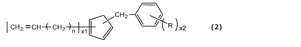
- the cyclopentadiene compound and / or its oligomer is not particularly limited, and examples of the cyclopentadiene compound include a cyclopentadiene compound represented by the following formula (2).
- R represents a group selected from an alkyl group having 1 to 6 carbon atoms, an alkenyl group having 2 to 6 carbon atoms, and an aryl group having 6 to 10 carbon atoms, and n is an integer of 1 to 4 carbon atoms.
- x1 and x2 are independently 0, 1 or 2, where if R represents an alkyl or aryl group, then x1 is 1 or 2 and 1 ⁇ x1 + x2 ⁇ 4.
- n is an integer of 1 to 4, preferably 1 to 2, and particularly preferably 1.
- x1 is 0, 1 or 2, preferably 0 or 1.
- x2 is 0, 1 or 2, preferably 1 or 2.
- R indicates a group selected from an alkyl group having 1 to 6 carbon atoms, an alkenyl group having 2 to 6 carbon atoms, and an aryl group having 6 to 10 carbon atoms.
- alkyl groups include methyl group, ethyl group, propyl group, isopropyl group, n-butyl group, isobutyl group, t-butyl group, n-pentyl group, isopentyl group, neopentyl group, t-pentyl group and n-.
- alkyl groups include methyl group, ethyl group, propyl group, isopropyl group, n-butyl group, isobutyl group, t-butyl group, n-pentyl group, isopentyl group, neopentyl group, t-pentyl group and n-.
- examples thereof include a hexyl group, an isohexyl
- alkenyl group examples include a vinyl group, an allyl group, an isopropenyl group, a butenyl group, a pentenyl group, a hexenyl group and the like.
- examples of the aryl group include a phenyl group, a tolyl group, a xylyl group, a mesityl group, a benzyl group, a biphenyl group, a naphthyl group and the like.
- R is preferably an alkenyl group, and a vinyl group and an allyl group are particularly preferable.
- x1 is 1 or 2, preferably 1 and 1 ⁇ x1 + x2 ⁇ 4, preferably 1 ⁇ x1 + x2 ⁇ 2.
- the compound represented by the formula (2) Since the cyclopentadiene ring of the compound represented by the formula (2) is highly reactive, the compound represented by the formula (2) is easily dimerized and / or trimerized by the Diels-Alder reaction to dimerize. Produces a body and / or a trimer.
- the dimerization or trimerization reaction may be a reaction of cyclopentadiene compounds having the same structure or a reaction of cyclopentadiene compounds having different structures from each other.
- the dimer ratio and oligomer ratio of the compound represented by the formula (2) are calculated from the area ratio of the peak measured by gel permeation chromatography (GPC).
- the oligomer of the compound represented by the formula (2) preferably has a dicyclopentadiene ring structure.
- the reaction in which the cyclopentadiene rings of the compound of the formula (2) react to form a dicyclopentadiene ring is cyclopentadiene. Since it is more likely to occur than the reaction between the ring and another Diels-Alder reactive carbon-carbon double bond, it is considered that the compound having the dicyclopentadiene ring is contained in a large amount in the component.
- the oligomer is a compound represented by the formula (2) at 50 to 200 ° C., preferably 60 to 180 ° C., more preferably 70 to 160 ° C., for 20 to 180 minutes, preferably 40 to 150 minutes. It is preferably obtained by heating for 60 to 120 minutes. This reaction is preferably carried out under vacuum.
- the heating of the compound represented by the formula (2) may be solvent-free, and may be carried out in a high boiling point solvent such as toluene, xylene or anisole if necessary.
- the compound represented by the formula (2) is prepared at 70 to 160 ° C. for 1 hour to 2 hours. It is preferable to heat under vacuum.
- the cyclopentadiene compound and / or its oligomer may be used alone or in combination of two or more.
- a polymerization initiator can be added to the cyclopentadiene compound and / or its oligomer, if necessary.
- the polymerization initiator include dicumyl peroxide, diisobutyl peroxide, di-t-butyl peroxide, 2,5-dimethyl-2,5-bis (t-butylperoxy) hexane, and di (2-t-butyl).
- Peroxyisopropyl) benzene and the like can be mentioned, and these may be used alone or in combination of two or more.
- the amount of the polymerization initiator (curing agent) added is not particularly limited, but is 0.2 to 5 parts by mass, preferably 0.5 to 3 parts by mass with respect to 100 parts by mass of the component (A).
- LDS additive Laser direct structuring additive
- the laser direct structuring additive (LDS additive) is added to a thermosetting resin, and the cured product is activated by an active energy ray such as a laser, so that only the irradiated portion is covered with a plating layer (B).
- a metal layer can be formed.
- the LDS additive is irradiated with an active energy ray such as a YAG laser having an absorbable wavelength region, the metal nuclei are activated (for example, reduced) to generate metal nuclei capable of metal plating. It is believed that.
- thermosetting resin composition in which the LDS additive is dispersed is irradiated with the above-mentioned active energy rays, a seed region having a metal nucleus capable of metal plating is formed on the irradiated surface. Will be done. By utilizing the obtained seed region, it becomes possible to form a plating pattern such as a circuit on the surface of the cured product of the thermosetting resin composition.
- the LDS additive is not particularly limited as long as it can form a metal core by irradiation with active energy rays, and for example, those described in Patent Documents 2 to 4 can be used.
- the following formula (1) is preferable.
- A is one or more metal elements selected from iron, copper, nickel, cobalt, zinc, magnesium and manganese
- B is iron, chromium or tungsten, where A and B are simultaneous. Not iron
- It is a metal oxide having a spinel structure, which is represented by the average composition formula of.
- the method for producing the metal oxide as these LDS additives is not limited, and those produced by firing the metal oxide mixed powder, oxidizing the metal powder mixture, chemically synthesizing, etc. may be used.
- the shape of the LDS additive is preferably fine particles, and the average particle size (median diameter (D50)) thereof is 0.01 to 5 ⁇ m in the volume particle size distribution measurement value measured by the laser diffraction type particle size distribution meter. Is preferable, and those in the range of 0.05 to 3.0 ⁇ m are particularly preferable.
- the average particle size of the LDS additive is 0.01 to 5 ⁇ m, the LDS additive is evenly distributed throughout the resin, and the generation of metal species that serve as a plating catalyst when the package surface is irradiated with a laser is promoted. The plating property is improved.
- the blending amount of the LDS additive is preferably 20 to 100 parts by mass, more preferably 30 to 80 parts by mass with respect to 100 parts by mass of the component (A).
- the amount is 20 parts by mass or more, the generation of metal nuclei serving as a plating catalyst when irradiated with a laser is sufficient, and the plating property is preferable. If it is 100 parts by mass or less, there is no possibility that parts other than the laser irradiation will be plated. Further, the proportion of the metal oxide particles having a small particle size becomes appropriate, and the fluidity and moldability of the composition become preferable.
- ⁇ Hexavalent chromium analysis method Dissolve 20 g of sodium hydroxide and 30 g of sodium carbonate in ion-exchanged water to prepare 1 liter of alkaline aqueous solution. The pH is 11.5 or higher. Weigh 2.5 g of the LDS additive into a clean container, add 1 mL of 40% magnesium chloride aqueous solution, 1 M phosphate buffer, and 50 mL of alkaline aqueous solution, and stir for 5 to 10 minutes. Shake in a water bath at 90-95 ° C. for 1 hour and let stand at room temperature for 20-40 minutes. Absorb 12 mL or more of the solution into a 30 mL syringe and filter with a 0.45 ⁇ m filter.
- Some grades of LDS additives are surface-treated with an inorganic material in order to improve dispersibility, but if a surface-treated product is used, the plating layer may be peeled off and the mechanical strength may be reduced. Therefore, a grade without surface treatment is desirable.
- Inorganic filler includes fused silica, crystalline silica, cristobalite, alumina, silicon nitride, aluminum nitride, boron nitride, titanium oxide, glass fiber, alumina fiber, zinc oxide, talc, calcium carbide and the like. Materials (however, excluding the above-mentioned component (B)) can be used. Two or more of these may be used in combination.
- the top cut diameter of the inorganic filler is preferably 5 to 25 ⁇ m, more preferably 10 to 20 ⁇ m in the wet sieving method, and the average particle size D50 is the volume particle size distribution measured value measured by the laser diffraction type particle size distribution meter. It is preferably 1 to 10 ⁇ m, more preferably 3 to 7 ⁇ m.
- the top cut diameter referred to here represents the mesh size of the sieve used in the classification of the manufactured inorganic filler by the wet sieving method, and the volume particle size measured by the laser diffraction method is the proportion of particles larger than the mesh size. A value that is 2% by volume or less in the distribution measurement value. If the top cut diameter is 25 ⁇ m or less, the exposed part of the surface of the inorganic filler will not be plated when irradiated with a laser or the like, or the plated metal layer and the inorganic filler will not be sufficiently bonded and will be easily peeled off. No problem occurs, and there is no risk of hindering the wiring layer or via production.
- the amount of the (C) inorganic filler added is preferably 50 to 1,500 parts by mass, more preferably 150 to 1,200 parts by mass with respect to 100 parts by mass of the component (A).
- the coupling agent of the component (D) is a triazine functional group type silane coupling agent, an isocyanate functional group type silane coupling agent, an isocyanuric acid functional group type silane coupling agent, and a benzotriazole functional group type silane. Selected from the group consisting of coupling agents, acid anhydride functional group type silane coupling agents, azasilacyclopentane functional group type silane coupling agents, imidazole functional group type silane coupling agents and unsaturated group-containing silane coupling agents.
- the (D) coupling agent is other than the mercaptosilane coupling agent, the aminosilane coupling agent and the epoxysilane coupling agent.
- Coupling agents with these functional groups are easy to coordinate with metal atoms contained in LDS additives such as copper and metal ions to be precipitated in the plating solution, and crosslink with thermosetting resins. It is useful for strengthening the bond of thermosetting resin. Further, since the alkoxy group bonded to the silicon atom can undergo a condensation reaction or hydrogen bond with the inorganic filler, it can also be bonded to the surface of the inorganic filler. Therefore, the plated metal layer has a strong bond with the cured product and does not easily come off. In addition, cracks do not occur due to mechanical stress and thermal stress.
- the isocyanate functional group in the isocyanate functional group type silane coupling agent may be a protected group (so-called blocked isocyanate group) or an unprotected group.
- the unsaturated group in the unsaturated group-containing silane coupling agent include an alkenyl group such as a vinyl group and an allyl group, a styryl group, a (meth) acrylic group, and a (meth) acrylic oxy group.
- Some coupling agents may be mixed with the inorganic component (C) in advance to treat the surface of the inorganic filler in advance.
- the amount of the component (D) added can be 0.3 parts by mass or more, for example, 0.5 to 8.0 parts by mass with respect to 100 parts by mass of the component (A). It is preferably 1.0 to 6.0 parts by mass, and more preferably 1.5 to 5.0 parts by mass. When the addition amount is 0.3 parts by mass or more, the bond formation with the metal in the LDS additive and the metal ion in the plating solution is sufficient. If it is 8.0 parts by mass or less, the amount of alcohol generated from the alkoxy group is not large, so that voids do not occur frequently and the electrical characteristics do not deteriorate.
- the resin composition of the present invention may further contain a mold release agent, a flame retardant, an ion trapping agent, a flexibility-imparting agent, a colorant and other additives, if necessary. ..
- waxes such as carnauba wax, rice wax, polyethylene, polyethylene oxide, montanic acid, montanic acid and saturated alcohol, 2- (2-hydroxyethylamino) -ethanol, ethylene glycol, ester compounds with glycerin and the like.
- examples thereof include stearic acid, stearic acid ester, stearic acid amide, ethylene bisstearic acid amide, and a copolymer of ethylene and vinyl acetate, which may be used alone or in combination of two or more.
- the flame retardant examples include halogenated epoxy resin, phosphazene compound, silicone compound, zinc molybdate-supported talc, zinc molybdate-supported zinc oxide, aluminum hydroxide, magnesium hydroxide, molybdenum oxide, antimony trioxide and the like. These flame retardants may be used alone or in combination of two or more, but a phosphazene compound, zinc molybdate-supported zinc oxide, and molybdenum oxide are preferably used from the viewpoint of environmental load and ensuring fluidity.
- Examples of the ion trapping agent include hydrotalcite compounds, bismuth compounds, zirconium compounds and the like, and these may be used alone or in combination of two or more.
- the flexibility-imparting agent examples include silicone compounds such as silicone oil, silicone resin, silicone-modified epoxy resin, and silicone-modified phenol resin, and thermoplastic elastomers such as styrene resin and acrylic resin. It may be used or two or more kinds may be used in combination.
- colorant examples include carbon black, titanium black, titanium oxide and the like, and these may be used alone or in combination of two or more.
- the content of these other additives in the resin composition may be appropriately determined within a range in which the functions of each additive are satisfactorily exhibited. For example, 0.1 with respect to 100 parts by mass of the component (A). It is in the range of 20 parts by mass or more and 20 parts by mass or less.
- thermosetting resin composition of the present invention is produced, for example, as follows. That is, a predetermined amount of each of a thermosetting resin, an LDS additive, an inorganic filler, a coupling agent and other materials is blended, and after sufficiently uniformly mixing with a mixer or the like, a heat roll, a kneader, an extruder or the like is used. It may be melt-mixed, then cooled and solidified, and pulverized to an appropriate size, and the obtained composition can be used as a molding material. It can also be locked and used as a tablet shape.
- the inorganic filler and the coupling agent may be mixed in whole or in part in advance.
- thermosetting resin composition of the present invention is a transistor type, a module type, a DIP type, an SO type, a flat pack type, a ball grid array type, a chip size package, a wafer level package, and a fan out. It is effective as a sealing resin for semiconductor devices such as packages.
- the method for sealing the semiconductor device with the thermosetting resin composition of the present invention is not particularly limited, and conventional molding methods such as transfer molding, injection molding, compression molding, and casting methods may be used.
- thermosetting resin composition of the present invention are not particularly limited, but are preferably 120 to 190 ° C. for 90 to 300 seconds. Further, it is preferable to perform post-cure at 170 to 250 ° C. for 2 to 16 hours.
- a metal layer can be easily and selectively provided by electroless plating by laser direct structuring on the surface or inside of the cured product of the thermosetting resin composition of the present invention, a communication device requiring electromagnetic wave shielding property.
- Devices that require an antenna circuit, devices that have a line circuit in a sealing resin layer instead of an organic substrate, and the like can be suitably used.
- the semiconductor device of the present invention has a cured product of the thermosetting resin composition of the present invention, and it is preferable that a part or all of the cured product is plated.
- the method of applying the plating treatment is not particularly limited, but an example will be described below.
- the surface of the cured product is irradiated with a laser beam selected from, for example, wavelengths of 185 nm, 248 nm, 254 nm, 308 nm, 355 nm, 532 nm, 1,064 nm or 10,600 nm so as to have a desired wiring and depth.
- the depth from the surface is 0 to 30 ⁇ m, preferably 0 to 20 ⁇ m.
- a laser beam selected from wavelengths of 185 nm, 248 nm, 254 nm, 308 nm, 355 nm, 532 nm, 1,064 nm or 10,600 nm is applied to a desired depth.
- irradiate so that the pore size is reached. Examples thereof include a method of immersing in a plating solution containing a target metal component such as Cu, Ni, and Ag after laser irradiation.
- the output of the laser is preferably 0.01 to 15 W, and the scanning speed of the laser is preferably in the range of 1 to 1,000 mm / s.
- the plating solution a solution containing a complexing agent, a pH adjuster, a conductivity salt, a reducing agent, etc., in addition to the target metal component, which is generally commercially available can be used.
- the temperature of the plating solution is 50 to 80 ° C., and the immersion time is 20 to 120 minutes.
- a metal layer is selectively and efficiently formed on the surface, cross section, or opening of the cured product without using an adhesive layer or an additional material such as a resist. Since the plating does not peel off and the cured product does not crack, the reliability is high.
- the semiconductor device of the present invention can be manufactured by a known LDS technique using the thermosetting resin composition of the present invention.
- LDS technology for example, those described in Patent Documents 2 to 4 and Japanese Patent No. 6423418 can be adopted.
- a semiconductor device in which a part or all of the cured product is plated can be manufactured by including a step of plating a part or all of the cured product and applying the plating treatment to a laser irradiation site. can.
- the plating process may be performed as described above.
- Such a method for manufacturing a semiconductor device is excellent in productivity because continuous production can be performed more effectively.
- Thermosetting resin / epoxy resin 1 Orthocresol novolac type epoxy resin: "Epicron N655EXP-S” manufactured by DIC (epoxy equivalent 210) -Epoxy resin 2: Biphenyl aralkyl type epoxy resin: "NC-3000” manufactured by Nippon Kayaku Co., Ltd. (epoxy equivalent 273) -Cyclic imide compound: Bismaleimide resin: "SLK-3000” manufactured by Shin-Etsu Chemical Co., Ltd.
- -Phenol resin 1 Novolac type phenol resin: "TD-2093Y” manufactured by DIC (phenol equivalent 110)
- -Phenol resin 2 Aralkyl type phenol resin: "MEHC-7851SS” manufactured by Meiwa Kasei Co., Ltd. (phenol equivalent 175)
- -Curing accelerator N'-[3-[[[(dimethylamino) carbonyl] amino] methyl] -3,5,5-trimethylcyclohexyl] -N, N-dimethylurea: "U-” manufactured by San-Apro. cat 3513N " -Polymerization initiator: Dicumyl peroxide: "Park Mill D” manufactured by NOF CORPORATION
- LDS additive / LDS additive 1 Shepherd Color Japan, Inc.
- LDS Additive 2 Made by Shepherd Color Japan Inc.
- EX-1815 (CuW 2 O 4 : Hexavalent chromium content less than 10 ppm): Average particle size 0.7 ⁇ m, no surface treatment
- LDS Additive 3 Made by Shepherd Color Japan Inc.
- Black 30C965 (CuCr 2 O 4 : Hexavalent chromium content 263 ppm): Average particle size 0.9 ⁇ m, with surface treatment]
- Inorganic filler / silica particles 1 "MUF-4" manufactured by Ryumori Co., Ltd. (average particle size 4 ⁇ m, top cut diameter 10 ⁇ m)
- Alumina particles 1 “AC9104-SXE” manufactured by Admatex (average particle size 4 ⁇ m, top cut diameter 10 ⁇ m)
- Examples 1 to 12 Comparative Examples 1 to 8
- Tables 1 and 2 The above components were blended according to the compositions (parts by mass) shown in Tables 1 and 2, and each component was melt-mixed, cooled and pulverized with respect to Examples 1 to 10 and Comparative Examples 1 to 7 to obtain a composition.
- each component was mixed with a sinky mixer and then kneaded with three rolls to obtain a viscous liquid.
- Tables 1 and 2 Each composition was evaluated according to the method shown below, and the results are shown in Tables 1 and 2.
- a glass epoxy printed wiring board having a thickness of 32 mm ⁇ 32 mm and a thickness of 1.6 mm was prepared by mounting a silicon chip having a thickness of 10 mm ⁇ 10 mm and a thickness of 0.75 mm.
- molding was performed under transfer conditions of 175 ° C., 6.9 N / mm 2 , and a cure time of 2 minutes, and then post-cure was performed at 175 ° C. for 2 hours to heat cure.
- a semiconductor device having a molding size of 28 mm ⁇ 28 mm and a molding thickness of 1.2 mm was produced.
- Comparative Example 8 was cast in a 28 mm ⁇ 28 mm Teflon (registered trademark) frame installed on a simulated semiconductor device, and cast at 300 ° C. at a temperature rise of 1 ° C./min under a nitrogen atmosphere.
- a semiconductor device having a thermosetting resin size of 28 mm ⁇ 28 mm and a thickness of 1.2 mm was produced.
- a YVO 4 laser marker manufactured by KEYENCE, 1064 nm
- 10 lines having a line width of 50 ⁇ m and a length of 10 mm were marked on the surface of the cured product at 1 mm intervals under the conditions of a speed of 1,000 mm / s and an output of 13 W. ..
- the semiconductor device was immersed in an electroless Cu plating solution heated to 65 ° C.: MID Copper 100XB (manufactured by MacDermid) for 20 minutes with stirring. After washing with water and drying, the resistance values at both ends of the plated wiring having a line width of 50 ⁇ m and a length of 10 mm formed on the surface of the cured product were measured, and the average value of 10 wires was recorded. It was also observed whether the wiring was short-circuited by plating other than the laser irradiation part.
- the cured product of the thermosetting resin composition of the present invention contains a specific (D) coupling agent, it has excellent conductivity of plated wiring, no short circuit between wirings (excellent surface plating property), and plating is possible. It did not peel off (excellent adhesion between the plating layer and the cured product), cracks did not occur in the semiconductor device in the temperature cycle test, and the plating property inside the through hole was also good.
- the component (D) having a specific functional group strengthens the bond between the LDS additive and the thermosetting resin and also bonds with the surface of the inorganic filler containing the alkoxy group bonded to the silicon atom. Therefore, the plated metal layer forms a strong bond with the cured product and does not easily detach.
- the composition of the present invention can form a metal layer with good adhesion on the surface of the cured product by electroless plating, and is compatible with crack resistance. Therefore, communication devices and antennas that require electromagnetic wave shielding properties. It is suitable for a semiconductor device including the above, and a semiconductor device for which it is necessary to form a wiring layer.
- the present invention is not limited to the above embodiment.
- the above-described embodiment is an example, and any of the above-described embodiments having substantially the same configuration as the technical idea described in the claims of the present invention and having the same effect and effect is the present invention. Is included in the technical scope of.
Landscapes
- Chemical & Material Sciences (AREA)
- Health & Medical Sciences (AREA)
- Chemical Kinetics & Catalysis (AREA)
- Medicinal Chemistry (AREA)
- Polymers & Plastics (AREA)
- Organic Chemistry (AREA)
- Compositions Of Macromolecular Compounds (AREA)
- Structures Or Materials For Encapsulating Or Coating Semiconductor Devices Or Solid State Devices (AREA)
Abstract
本発明は、(A)熱硬化性樹脂、(B)レーザーダイレクトストラクチャリング添加剤、(C)無機充填材、及び(D)カップリング剤を含む熱硬化性樹脂組成物であって、前記(D)カップリング剤が、トリアジン官能基型、イソシアネート官能基型、イソシアヌル酸官能基型、ベンゾトリアゾール官能基型、酸無水物官能基型、アザシラシクロペンタン官能基型、イミダゾール官能基型及び不飽和基含有シランカップリング剤からなる群から選択される一種以上を含み、かつ、メルカプトシランカップリング剤、アミノシランカップリング剤及びエポキシシランカップリング剤以外のものであることを特徴とする熱硬化性樹脂組成物である。これにより、硬化物の表面に形成されたメッキ層が硬化物から剥がれず、またクラックも発生しない硬化物を与える熱硬化性樹脂組成物が提供される。
Description
本発明は、無電解メッキなどにより硬化物表面、硬化物断面及び開口部に、被覆層又は配線層を作製可能な、熱硬化性樹脂組成物、その硬化物及び該硬化物を有する半導体装置に関する。
携帯電話、スマートフォン等の通信機器に搭載される半導体装置では、機器が発する電磁ノイズによる誤動作を防ぐため、電磁波シールド性を持たせる必要がある。
半導体装置に電磁波シールド性をもたせる方法として、板金による方法、スパッタにより半導体表面に金属層を蒸着する方法等がある。しかし、板金により電磁波シールド性をもたせる方法は、通信機器の薄型化・小型化に適さず、またスパッタにより金属層を蒸着する方法は、その過程で高真空にする必要があり、連続生産ができず生産性に劣るものである。
半導体装置に電磁波シールド性をもたせる方法として、板金による方法、スパッタにより半導体表面に金属層を蒸着する方法等がある。しかし、板金により電磁波シールド性をもたせる方法は、通信機器の薄型化・小型化に適さず、またスパッタにより金属層を蒸着する方法は、その過程で高真空にする必要があり、連続生産ができず生産性に劣るものである。
また、ウェアラブルデバイス等の発展に伴い、半導体装置もさらなる薄型化が要求されている。そこで、半導体封止材の表面にメッキによる金属配線パターンを形成することで、半導体装置の上に新たな半導体装置を直接作製可能となる。
また、配線以外にも半導体封止材の表面にアンテナを形成することで通信機器向け半導体装置の小型化も試みられている。
そうした開発の一環として、近年ではウェハーレベル封止のチップサイズパッケージにおいて、再配線層をチップの外側に設けることで、複数のチップ間を高密度の配線で接続できる技術が開発されている。しかし、現在の再配線に用いられる方式としては、銅電解メッキなどが主流であり、レジストの塗布、パターン形成、洗浄、スパッタ、レジストの除去、電解メッキと工程が非常に煩雑である。また電解メッキによる方法では、樹脂やチップに対しても耐薬品性が求められている。
そうした中、選択的にメッキパターンを構築する方法として、レーザーダイレクトストラクチャリング(以下「LDS」と記載する)という技術が開発されている(特許文献1)。この技術ではLDS添加剤を熱可塑性樹脂に添加し、その硬化物をレーザーにて活性化することで、照射した部分のみにメッキ層(金属層)を形成できる。この技術では接着層や、レジスト等を用いずに硬化物表面、断面、または開口部に金属層の形成が可能という特徴がある(特許文献2、3)。
また熱可塑樹脂だけではなく熱硬化性樹脂にLDS添加剤を添加し、メッキ付き特性に優れたLDS用熱硬化性樹脂組成物や、それを用いた三次元成形回路部品も開発されている(特許文献4)。
しかしながらメッキ後の金属配線が硬化物から剥がれてしまうという問題や、硬化物にクラックが発生するという問題も生じる。原因として、メッキ金属析出の核となるLDS添加剤と熱硬化性樹脂の結合が弱いこと、及び析出したメッキ金属と熱硬化性樹脂の結合が弱いことが考えられる。結合が十分でないと、レーザー照射によるLDS活性化工程、及びアルカリ性無電解メッキの工程でLDS添加剤と熱硬化性樹脂の界面、及び析出したメッキ金属と熱硬化性樹脂の界面にミクロンオーダーの隙間が生じ、メッキ後の金属層が硬化物から剥離しやすくなる。また硬化物に機械応力、または熱応力がかかった時、隙間を起点にクラックが発生するためと考えられる。
しかしながらメッキ後の金属配線が硬化物から剥がれてしまうという問題や、硬化物にクラックが発生するという問題も生じる。原因として、メッキ金属析出の核となるLDS添加剤と熱硬化性樹脂の結合が弱いこと、及び析出したメッキ金属と熱硬化性樹脂の結合が弱いことが考えられる。結合が十分でないと、レーザー照射によるLDS活性化工程、及びアルカリ性無電解メッキの工程でLDS添加剤と熱硬化性樹脂の界面、及び析出したメッキ金属と熱硬化性樹脂の界面にミクロンオーダーの隙間が生じ、メッキ後の金属層が硬化物から剥離しやすくなる。また硬化物に機械応力、または熱応力がかかった時、隙間を起点にクラックが発生するためと考えられる。
本発明は、上記問題を解決するためになされたものであり、熱硬化性樹脂組成物であって、該組成物の硬化物の表面、断面、又は開口部に形成されたメッキ層は硬化物から剥がれることがなく、また、硬化物にクラックも発生しない熱硬化性樹脂組成物の提供を目的とする。
上記課題を解決するために、本発明では、
(A)熱硬化性樹脂、
(B)レーザーダイレクトストラクチャリング添加剤、
(C)無機充填材、及び
(D)カップリング剤
を含む熱硬化性樹脂組成物であって、
前記(D)カップリング剤が、トリアジン官能基型シランカップリング剤、イソシアネート官能基型シランカップリング剤、イソシアヌル酸官能基型シランカップリング剤、ベンゾトリアゾール官能基型シランカップリング剤、酸無水物官能基型シランカップリング剤、アザシラシクロペンタン官能基型シランカップリング剤、イミダゾール官能基型シランカップリング剤及び不飽和基含有シランカップリング剤からなる群から選択される一種以上を含み、かつ、前記(D)カップリング剤が、メルカプトシランカップリング剤、アミノシランカップリング剤及びエポキシシランカップリング剤以外のものであることを特徴とする熱硬化性樹脂組成物を提供する。
本発明の熱硬化性樹脂組成物であれば、その硬化物の表面、断面、又は開口部に形成されたメッキ層は硬化物から剥がれることがなく、また、硬化物にクラックも発生しない。
また、本発明では、前記(B)成分が、下記式(1)
AB2O4 (1)
(式中、Aは鉄、銅、ニッケル、コバルト、亜鉛、マグネシウム及びマンガンから選ばれる1種もしくは2種以上の金属元素であり、Bは鉄、クロム又はタングステンであり、ただしA及びBは同時に鉄ではない)
の平均組成式で示され、スピネル構造を有する金属酸化物であることが好ましい。
AB2O4 (1)
(式中、Aは鉄、銅、ニッケル、コバルト、亜鉛、マグネシウム及びマンガンから選ばれる1種もしくは2種以上の金属元素であり、Bは鉄、クロム又はタングステンであり、ただしA及びBは同時に鉄ではない)
の平均組成式で示され、スピネル構造を有する金属酸化物であることが好ましい。
このような(B)成分は、LDS添加剤として熱可塑性樹脂組成物に添加すると、その硬化物をレーザー等にて活性化することで、照射した部分のみにメッキ層(金属層)を効率よく形成できる。
また、本発明では、前記(B)成分中の6価クロムの含有量が100ppm未満であることが好ましい。
このような(B)成分を含む熱硬化性樹脂組成物であれば、電子電気機器における特定有害物質の使用制限についての欧州連合(EU)による指令(RoHS指令)に適合し、廃電気・電子機器のリサイクルを容易にすることができる。
また、本発明では、前記(B)成分が表面処理されていないレーザーダイレクトストラクチャリング添加剤であることが好ましい。
このような(B)成分は、表面処理がなされていないため、メッキ層の剥離、機械強度の低下を引き起こしにくい。
また、本発明では、前記(A)熱硬化性樹脂が、(i)エポキシ樹脂、(ii)1分子中に、1つ以上のダイマー酸骨格、1つ以上の炭素数6以上の直鎖アルキレン基、及び2つ以上の環状イミド基を含有する環状イミド化合物、(iii)1分子中に2個以上のシアナト基を有するシアネートエステル化合物、(iv)下記式(2)

(式(2)中、Rは炭素数1~6のアルキル基、炭素数2~6のアルケニル基、及び炭素数6~10のアリール基から選ばれる基を示し、nは1~4の整数であり、x1及びx2は独立して0、1又は2であり、ただし、Rがアルキル基又はアリール基を示す場合は、x1は1又は2であり、かつ、1≦x1+x2≦4である)
で示されるシクロペンタジエン化合物及び/又はそのオリゴマーから選択される一種類または二種類以上を含むものであることが好ましい。
で示されるシクロペンタジエン化合物及び/又はそのオリゴマーから選択される一種類または二種類以上を含むものであることが好ましい。
このような樹脂が(A)成分として好適に使用できる。
また、本発明は上記熱硬化性樹脂組成物が硬化してなるものであることを特徴とする硬化物を提供する。
このような硬化物は、その表面、断面、又は開口部に形成されたメッキ層が硬化物から剥がれることがなく、また、硬化物にクラックも発生しないため、電磁波シールド性を必要とする通信デバイスや、アンテナ若しくは配線層を備える半導体装置等の封止材として有用である。
また、本発明は、上記硬化物を有するものであることを特徴とする半導体装置を提供する。
本発明の半導体装置は、上記硬化物を有するためアンテナや配線層等の金属層の密着性に優れるとともに、連続生産が可能であり、生産性に優れている。
この場合、前記硬化物の一部または全部がメッキ処理されているものであることが好ましい。
このようなものであれば、接着層や、レジスト等を用いずに硬化物の表面、断面、または開口部に金属層の形成が選択的かつ効率的になされるとともに、メッキの剥がれや、硬化物にクラックが生じることもないため、信頼性の高いものとなる。
さらに本発明は、上記半導体装置の製造方法であって、前記硬化物の一部または全部をメッキ処理する工程を含み、前記メッキ処理がレーザー照射箇所に施されることを特徴とする半導体装置の製造方法を提供する。
このような半導体装置の製造方法であれば、連続生産がより効果的に行えるため、生産性に優れている。
本発明の熱硬化性樹脂組成物は、LDS添加剤及び析出したメッキ金属と熱硬化性樹脂の界面の結合が強い硬化物を与える組成物であって、無電解メッキ処理等によりその硬化物の表面又は内部に金属層(メッキ層等)を、選択的かつ容易に形成できる。この金属層(メッキ層等)は硬化物と強固な結合を有しており容易に脱離しない。また機械的応力や熱応力によってクラックが発生しない。したがって、本発明の熱硬化性樹脂組成物は、小型で薄型の、電磁波シールド性を必要とする通信デバイス、アンテナを備える半導体装置及び配線層を備える半導体装置等の封止材として好適である。また、本発明の組成物の硬化物を有する半導体装置は、連続生産が可能であり、生産性に優れる。
上述のように、LDS添加剤及び形成した金属層と熱硬化性樹脂の界面の結合が強い硬化物を与える熱硬化性樹脂組成物の開発が求められていた。
本発明者らは、上記課題解決のため鋭意研究したところ、LDS添加剤を含む熱硬化性樹脂組成物において、特定構造のシランカップリング剤を用いることで、LDS添加剤と熱硬化性樹脂の界面の結合を高めることができることを見出し、本発明を完成させた。
すなわち、本発明は、下記熱硬化性樹脂組成物と該組成物の硬化物、及び該硬化物を有する半導体装置を提供するものである。
すなわち、本発明は、下記熱硬化性樹脂組成物と該組成物の硬化物、及び該硬化物を有する半導体装置を提供するものである。
以下、本発明について詳細に説明するが、本発明はこれらに限定されるものではない。
本発明の熱硬化性樹脂組成物は、(A)熱硬化性樹脂、(B)レーザーダイレクトストラクチャリング添加剤、(C)無機充填材、及び(D)カップリング剤を含む熱硬化性樹脂組成物であって、前記(D)カップリング剤が、トリアジン官能基型シランカップリング剤、イソシアネート官能基型シランカップリング剤、イソシアヌル酸官能基型シランカップリング剤、ベンゾトリアゾール官能基型シランカップリング剤、酸無水物官能基型シランカップリング剤、アザシラシクロペンタン官能基型シランカップリング剤、イミダゾール官能基型シランカップリング剤及び不飽和基含有シランカップリング剤からなる群から選択される一種以上を含み、かつ、前記(D)カップリング剤が、メルカプトシランカップリング剤、アミノシランカップリング剤及びエポキシシランカップリング剤以外のものであることを特徴とする。必要に応じて上記(A)~(D)成分以外の成分を更に含むことができる。
以下、各成分について説明する。
以下、各成分について説明する。
[(A)熱硬化性樹脂]
本発明の熱硬化性樹脂組成物は、(A)熱硬化性樹脂を含有するものである。
上記熱硬化性樹脂としては、例えば、たとえばエポキシ樹脂、フェノール樹脂、1分子中に、少なくとも1つのダイマー酸骨格、少なくとも1つの炭素数6以上の直鎖アルキレン基、及び少なくとも2つの環状イミド基を含有する環状イミド化合物、1分子中に2個以上のシアナト基を有するシアネートエステル化合物、シクロペンタジエン化合物及び/又はそのオリゴマー、オキセタン樹脂、(メタ)アクリレート樹脂、末端(メタ)アクリル基変性ポリフェニレンエーテル樹脂、不飽和ポリエステル樹脂、ジアリルフタレート樹脂、およびマレイミド樹脂等から選択される一種類または二種類以上を含む樹脂とすることができる。
これらの中でも、(i)エポキシ樹脂、(ii)1分子中に、1つ以上のダイマー酸骨格、1つ以上の炭素数6以上の直鎖アルキレン基、及び2つ以上の環状イミド基を含有する環状イミド化合物、(iii)1分子中に2個以上のシアナト基を有するシアネートエステル化合物、(iv)シクロペンタジエン化合物及び/又はそのオリゴマーを含むものであることが好ましい。
エポキシ樹脂としては、特に限定されないが、半導体封止用エポキシ樹脂組成物の技術分野で従来使用されるエポキシ樹脂が挙げられる。このようなエポキシ樹脂としては、フェノールノボラック型エポキシ樹脂、オルソクレゾールノボラック型エポキシ樹脂、ナフトールノボラック型エポキシ樹脂、ビフェニル型エポキシ樹脂、ビスフェノール型エポキシ樹脂、スチルベン型エポキシ樹脂、ジヒドロアントラセンジオール型エポキシ樹脂等の結晶性エポキシ樹脂、トリフェノールメタン型エポキシ樹脂、アルキル変性トリフェノールメタン型エポキシ樹脂等の多官能エポキシ樹脂、フェニレン骨格を有するフェノールアラルキル型エポキシ樹脂、ビフェニレン骨格を有するビフェニルアラルキル型エポキシ樹脂、フェニレン骨格を有するナフトールアラルキル型エポキシ樹脂、ビフェニレン骨格を有するナフトールビフェニルアラルキル型エポキシ樹脂等のアラルキル型エポキシ樹脂、ジヒドロキシナフタレン型エポキシ樹脂、ジヒドロキシナフタレンの二量体をグリシジルエーテル化して得られるエポキシ樹脂等のナフトール型エポキシ樹脂、トリグリシジルイソシアヌレート、モノアリルジグリシジルイソシアヌレート等のトリアジン核含有エポキシ樹脂、ジシクロペンタジエン変性フェノール型エポキシ樹脂等の環状炭化水素化合物変性フェノール型エポキシ樹脂等が挙げられ、これらは1種単独で用いても2種以上を併用してもよい。これらのうち、組成物の粘度を低く抑えるため、オルソクレゾールノボラック型エポキシ樹脂等のノボラック型エポキシ樹脂、ビフェニルアラルキル型エポキシ樹脂等のアラルキル型エポキシ樹脂及びビフェニル型エポキシ樹脂が好ましい。
エポキシ樹脂は硬化剤を併用することができる。硬化剤としては、フェノール樹脂、酸無水物、アミン、活性エステル等を使用することができる。この中でも耐熱性、耐湿性からフェノール樹脂が好ましい。フェノール樹脂としては、ノボラック型フェノール樹脂、ナフタレン環含有フェノール樹脂、アラルキル型ビフェニル樹脂、アラルキル型フェノール樹脂、トリフェノールアルカン型フェノール樹脂、ビフェニル型フェノール樹脂、脂環式フェノール樹脂、複素環型フェノール樹脂、ナフタレン環含有フェノール樹脂、ビスフェノールA型フェノール樹脂、ビスフェノールF型フェノール樹脂等のビスフェノール型フェノール樹脂が挙げられ、これらは1種単独で用いても2種以上を併用してもよい。これらのうち、好ましくはノボラック型フェノール樹脂、アラルキル型ビフェニル樹脂、アラルキル型フェノール樹脂、ビフェニルアラルキル型フェノール樹脂であり、特に好ましくはアラルキル型フェノール樹脂である。
エポキシ樹脂と硬化剤との配合割合(エポキシ基/フェノール性水酸基)は、当量比で、0.5以上1.5以下が好ましく、0.8以上1.2以下がより好ましい。この配合割合の範囲であれば、硬化剤が適切で経済的に有利となり、硬化不足にならない。
エポキシ樹脂とフェノール樹脂の硬化促進剤としては、2-メチルイミダゾール、2-エチル-4-メチルイミダゾール、2-メチル-4-エチルイミダゾール、2-フェニルイミダゾール、2-メチル-4-メチルイミダゾール等のイミダゾール類;1,8-ジアザビシクロ[5.4.0]ウンデセン-7、トリエチレンジアミン、ベンジルジメチルアミン等の三級アミン類;トリフェニルホスフィン、トリブチルホスフィン、テトラフェニルホスホニウム・テトラフェニルボレート等の有機ホスフィン類等及び、これらをマイクロカプセル化したもの、N,N,N’,N’-テトラメチルウレア、N’-フェニル-N,N-ジメチルウレア、N,N-ジエチルウレア、N’-[3-[[[(ジメチルアミノ)カルボニル]アミノ]メチル]-3,5,5-トリメチルシクロへキシル]-N,N-ジメチルウレア、N,N”-(4-メチル-1,3-フェニレン)ビス(N’,N’-ジメチルウレア)等ウレア構造を有する化合物が挙げられ、これらは1種単独で用いても、2種以上を併用してもよい。
中でも、一定の温度に達してはじめて硬化反応を起こす潜在性を有することから、N,N-ジエチルウレア、N’-[3-[[[(ジメチルアミノ)カルボニル]アミノ]メチル]-3,5,5-トリメチルシクロへキシル]-N,N-ジメチルウレアが好ましい。
硬化促進剤の添加量としては、(A)エポキシ樹脂とフェノール樹脂成分の合計100質量部に対して、0.5~10.0質量部が好ましく、1.5~6.0質量部がより好ましい。この範囲内であれば、エポキシ基とフェノール性水酸基が速やかに反応し、容易に硬化物を得ることができる。
環状イミド化合物としては、特に限定されないが、1分子中に、1つ以上のダイマー酸骨格、1つ以上の炭素数6以上の直鎖アルキレン基、及び2つ以上の環状イミド基を含有する環状イミド化合物が挙げられる。また、環状イミド化合物としてはマレイミド化合物が好ましく、中でも下記一般式(3)で表されるマレイミド化合物がより好ましい。なお、下記式中のA、Bはこの式においてのみ適用されるものとする。

(一般式(3)中、Aは独立して芳香族環又は脂肪族環を含む4価の有機基を示す。Bは2価のヘテロ原子を含んでもよい脂肪族環を有する炭素数6から18のアルキレン基である。Qは独立して炭素数6以上の直鎖アルキレン基を示す。R’は夫々独立に炭素数6以上の直鎖又は分岐鎖のアルキル基を示す。lは1~10の数を表す。mは0~10の数を表す。)
一般式(3)のQは直鎖のアルキレン基であり、これらの炭素数は6以上であるが、好ましくは6以上20以下であり、より好ましくは7以上15以下である。
また、一般式(3)中のR’はアルキル基であり、直鎖のアルキル基でも分岐のアルキル基でもよく、これらの炭素数は6以上であるが、好ましくは6以上12以下である。
また、一般式(3)中のR’はアルキル基であり、直鎖のアルキル基でも分岐のアルキル基でもよく、これらの炭素数は6以上であるが、好ましくは6以上12以下である。
一般式(3)中のAは芳香族環又は脂肪族環を含む4価の有機基を示し、特に、下記構造式で示される4価の有機基のいずれかであることが好ましい。

(なお、上記構造式中の置換基が結合していない結合手は、一般式(3)において環状イミド構造を形成するカルボニル炭素と結合するものである。)
また、一般式(3)中のBは2価のヘテロ原子を含んでもよい脂肪族環を有する炭素数6から18のアルキレン基であり、該アルキレン基の炭素数は好ましくは炭素数8以上15以下である。一般式(3)中のBは下記構造式で示される脂肪族環を有するアルキレン基のいずれかであることが好ましい。

(なお、上記構造式中の置換基が結合していない結合手は、一般式(3)において環状イミド構造を形成する窒素原子と結合するものである。)
一般式(3)中のlは1~10の数であり、好ましくは2~7の数である。一般式(3)中のmは0~10の数であり、好ましくは0~7の数である。
環状イミド化合物の重量平均分子量(Mw)は、室温(25℃)での性状を含めて特に制限はないが、ゲルパーミエーションクロマトグラフィ(GPC)測定によるポリスチレン標準で換算した重量平均分子量が70,000以下であることが好ましく、より好ましくは1,000以上50,000以下である。該分子量が70,000以下であれば、得られる組成物は粘度が高くなりすぎて流動性が低下するおそれがなく、ラミネート成形などの成形性が良好となる。
なお、本発明中で言及する重量平均分子量(Mw)とは、下記条件で測定したGPCによるポリスチレンを標準物質とした重量平均分子量を指すこととする。
[測定条件]
展開溶媒:テトラヒドロフラン
流量:0.35mL/min
検出器:RI
カラム:TSK-GEL Hタイプ(東ソー株式会社製)
カラム温度:40℃
試料注入量:5μL
[測定条件]
展開溶媒:テトラヒドロフラン
流量:0.35mL/min
検出器:RI
カラム:TSK-GEL Hタイプ(東ソー株式会社製)
カラム温度:40℃
試料注入量:5μL
環状イミド化合物としては、相当する酸無水物とジアミンとの重合反応により合成してもよいし、BMI-1500、BMI-3000、BMI-5000(以上、Designer Molecules Inc.製)、SLK-1500、SLK-3000、SLK-2600(以上、信越化学工業(株)製)等の市販品を用いてもよい。また、環状イミド化合物は1種単独で使用しても、2種類以上を併用しても構わない。
環状イミド化合物には、必要に応じて重合開始剤を添加することができる。
重合開始剤としては、ジクミルパーオキシド、ジイソブチルパーオキサイド、ジ-t-ブチルパーオキサイド、2,5-ジメチル-2,5-ビス(t-ブチルパーオキシ)ヘキサン、ジ(2-t-ブチルパーオキシイソプロピル)ベンゼン等が挙げられ、これらは1種単独で用いても2種以上を併用してもよい。
重合開始剤としては、ジクミルパーオキシド、ジイソブチルパーオキサイド、ジ-t-ブチルパーオキサイド、2,5-ジメチル-2,5-ビス(t-ブチルパーオキシ)ヘキサン、ジ(2-t-ブチルパーオキシイソプロピル)ベンゼン等が挙げられ、これらは1種単独で用いても2種以上を併用してもよい。
重合開始剤(硬化剤)の添加量は特に制限されないが、(A)成分100質量部に対し、0.2~5質量部、好ましくは0.5~3質量部である。
シアネートエステル化合物は、特に限定されないが、1分子中に2個以上のシアナト基を有するものであればよく、一般に公知のものが使用できる。該シアネートエステル化合物は、例えば下記一般式(4)で表すことができる。

(式中、R1及びR2は、互いに独立に、水素原子または炭素数1~4のアルキル基であり、R3は、互いに独立に、下記のいずれかである。

(式中、R4は水素原子またはメチル基である。kは0~10の整数である。)
シアネートエステル化合物としては、例えば、ビス(4-シアナトフェニル)メタン、ビス(3-メチル-4-シアナトフェニル)メタン、ビス(3-エチル-4-シアナトフェニル)メタン、ビス(3,5-ジメチル-4-シアナトフェニル)メタン、1,1-ビス(4-シアナトフェニル)エタン、2,2-ビス(4-シアナトフェニル)プロパン、2,2-ビス(4-シアナトフェニル)-1,1,1,3,3,3-ヘキサフルオロプロパン、1,3-および1,4-ジシアナトベンゼン、2-tert-ブチル-1,4-ジシアナトベンゼン、2,4-ジメチル-1,3-ジシアナトベンゼン、2,5-ジ-tert-ブチル-1,4-ジシアナトベンゼン、テトラメチル-1,4-ジシアナトベンゼン、1,3,5-トリシアナトベンゼン、2,2’-または4,4’-ジシアナトビフェニル、3,3’,5,5’-テトラメチル-4,4’-ジシアナトビフェニル、1,3-、1,4-、1,5-、1,6-、1,8-、2,6-、または2,7-ジシアナトナフタレン、1,3,6-トリシアナトナフタレン、1,1,1-トリス(4-シアナトフェニル)エタン、ビス(4-シアナトフェニル)エーテル、4,4’-(1,3-フェニレンジイソプロピリデン)ジフェニルシアネート、ビス(4-シアナトフェニル)チオエーテル、ビス(4-シアナトフェニル)スルホン、トリス(4-シアナト-フェニル)ホスフィン、トリス(4-シアナトフェニル)ホスフェート、フェノールノボラック型シアネート、クレゾールノボラック型シアネート、ジシクロペンタジエンノボラック型シアネート、フェニルアラルキル型シアネートエステル、ビフェニルアラルキル型シアネートエステル、ナフタレンアラルキル型シアネートエステルなどが挙げられる。これらのシアネートエステル化合物は1種または2種以上混合して用いることができる。
また、シアネート基の当量が小さいもの、即ち官能基間分子量が小さいものは硬化収縮が小さく、低熱膨張、高Tgの硬化物を得ることができる。シアネート基当量が大きいものは若干Tgが低下するが、トリアジン架橋間隔がフレキシブルになり、低弾性化、高強靭化、低吸水化が期待できる。シアネートエステル化合物中に結合あるいは残存している塩素は50ppm以下、より好ましくは20ppm以下であることが好適である。塩素の量が50ppm以下であれば高温下に長期間置いたときに熱分解により遊離した塩素あるいは塩素イオンが、酸化されたCuフレームやCuワイヤー、Agメッキを腐食し、硬化物の剥離や電気的不良を引き起こすことがなく、また樹脂の絶縁性も低下しない。
シアネートエステル化合物には必要に応じて硬化剤を添加することができる。
硬化剤としては前述のフェノール樹脂を用いることができる。
硬化剤としては前述のフェノール樹脂を用いることができる。
シクロペンタジエン化合物及び/又はそのオリゴマーとしては、特に限定されないが、シクロペンタジエン化合物としては下記式(2)で示されるシクロペンタジエン化合物を挙げることができる。
(式(2)中、Rは炭素数1~6のアルキル基、炭素数2~6のアルケニル基、及び炭素数6~10のアリール基から選ばれる基を示し、nは1~4の整数であり、x1及びx2は独立して0、1又は2であり、ただし、Rがアルキル基又はアリール基を示す場合は、x1は1又は2であり、かつ、1≦x1+x2≦4である。)
前記式(2)において、nは1~4の整数であり、好ましくは1~2であり、特に好ましくは1である。x1は0、1又は2であり、好ましくは0又は1である。x2は0、1又は2であり、好ましくは1又は2である。
また、Rは炭素数1~6のアルキル基、炭素数2~6のアルケニル基、及び炭素数6~10のアリール基から選ばれる基を示す。アルキル基の例としては、メチル基、エチル基、プロピル基、イソプロピル基、n-ブチル基、イソブチル基、t-ブチル基、n-ペンチル基、イソペンチル基、ネオペンチル基、t-ペンチル基、n-ヘキシル基、イソヘキシル基、シクロペンチル基、シクロヘキシル基等が挙げられる。
また、アルケニル基の例としては、ビニル基、アリル基、イソプロペニル基、ブテニル基、ペンテニル基、ヘキセニル基等が挙げられる。
さらに、アリール基の例としては、フェニル基、トリル基、キシリル基、メシチル基、ベンジル基、ビフェニル基、ナフチル基等が挙げられる。
中でも、Rはアルケニル基であることが好ましく、ビニル基、アリル基が特に好ましい。
なお、Rがアルキル基又はアリール基を示す場合は、x1は1又は2であり、好ましくは1であり、かつ、1≦x1+x2≦4であり、好ましくは1≦x1+x2≦2である。
なお、Rがアルキル基又はアリール基を示す場合は、x1は1又は2であり、好ましくは1であり、かつ、1≦x1+x2≦4であり、好ましくは1≦x1+x2≦2である。
前記式(2)で示される化合物のシクロペンタジエン環は反応性に富むため、前記式(2)で示される化合物は、Diels-Alder反応により、容易に二量化及び/又は三量化し、二量体及び/又は三量体を生成する。なお、前記二量化や三量化の反応は、同じ構造のシクロペンタジエン化合物の反応であっても、互いに異なった構造のシクロペンタジエン化合物の反応であってもよい。
なお、式(2)で示される化合物の二量体割合及びオリゴマー割合は、ゲルパーミエーションクロマトグラフィ(GPC)測定によるピークの面積比から算出したものである。
なお、式(2)で示される化合物の二量体割合及びオリゴマー割合は、ゲルパーミエーションクロマトグラフィ(GPC)測定によるピークの面積比から算出したものである。
また、式(2)で示される化合物のオリゴマーは、ジシクロペンタジエン環構造を有するものが好ましい。
前記式(2)の化合物のシクロペンタジエン環が反応してジシクロペンタジエン環を形成する反応、すなわち、2分子の式(2)の化合物中のシクロペンタジエン環同士のDiels-Alder反応は、シクロペンタジエン環と他のDiels-Alder反応可能な炭素-炭素二重結合との反応よりも起こりやすいため、前記ジシクロペンタジエン環を有する化合物は、成分中に多く含まれていると考えられる。
前記オリゴマーの構造としては、下記式のようなものが例示できる。

(式中、R、n、x1、及びx2はそれぞれ前記と同じである。)


前記オリゴマーは、式(2)で示される化合物を、50~200℃、好ましくは60~180℃、より好ましくは70~160℃で、20分~180分間、好ましくは40分~150分間、より好ましくは60分~120分間加熱することにより得られる。この反応は、真空下で行なうことが好ましい。
また、式(2)で示される化合物の加熱は、無溶媒でよく、必要であればトルエン、キシレン、アニソールなどの高沸点溶媒中で行うことができる。
成分中、式(2)で示されるシクロペンタジエン化合物の二量体を3質量%以上とするためには、式(2)で示される化合物を、70~160℃で、1時間~2時間、真空下で加熱することが好ましい。
シクロペンタジエン化合物及び/又はそのオリゴマーは1種単独で使用しても2種類以上を併用しても構わない。
シクロペンタジエン化合物及び/又はそのオリゴマーには、必要に応じて重合開始剤を添加することができる。
重合開始剤としては、ジクミルパーオキシド、ジイソブチルパーオキサイド、ジ-t-ブチルパーオキサイド、2,5-ジメチル-2,5-ビス(t-ブチルパーオキシ)ヘキサン、ジ(2-t-ブチルパーオキシイソプロピル)ベンゼン等が挙げられ、これらは1種単独で用いても2種以上を併用してもよい。
重合開始剤としては、ジクミルパーオキシド、ジイソブチルパーオキサイド、ジ-t-ブチルパーオキサイド、2,5-ジメチル-2,5-ビス(t-ブチルパーオキシ)ヘキサン、ジ(2-t-ブチルパーオキシイソプロピル)ベンゼン等が挙げられ、これらは1種単独で用いても2種以上を併用してもよい。
重合開始剤(硬化剤)の添加量は特に制限されないが、(A)成分100質量部に対し、0.2~5質量部、好ましくは0.5~3質量部である。
(B)レーザーダイレクトストラクチャリング添加剤(LDS添加剤)
(B)レーザーダイレクトストラクチャリング添加剤(LDS添加剤)は、熱硬化性樹脂に添加し、その硬化物をレーザー等の活性エネルギー線にて活性化することで、照射した部分のみにメッキ層(金属層)を形成可能とするものである。LDS添加剤は、吸収可能な波長領域を有するYAGレーザー等の活性エネルギー線が照射されると、金属核が活性化して(例えば、還元されて)、金属めっきが可能な金属核が生成されると考えられている。そして、LDS添加剤が分散された熱硬化性樹脂組成物の硬化物の表面に対して上記活性エネルギー線を照射すると、その照射面に、金属メッキを可能とする金属核を有するシード領域が形成される。得られたシード領域を利用することにより、熱硬化性樹脂組成物の硬化物の表面に、回路などのめっきパターンを形成することが可能になる。
(B)レーザーダイレクトストラクチャリング添加剤(LDS添加剤)は、熱硬化性樹脂に添加し、その硬化物をレーザー等の活性エネルギー線にて活性化することで、照射した部分のみにメッキ層(金属層)を形成可能とするものである。LDS添加剤は、吸収可能な波長領域を有するYAGレーザー等の活性エネルギー線が照射されると、金属核が活性化して(例えば、還元されて)、金属めっきが可能な金属核が生成されると考えられている。そして、LDS添加剤が分散された熱硬化性樹脂組成物の硬化物の表面に対して上記活性エネルギー線を照射すると、その照射面に、金属メッキを可能とする金属核を有するシード領域が形成される。得られたシード領域を利用することにより、熱硬化性樹脂組成物の硬化物の表面に、回路などのめっきパターンを形成することが可能になる。
(B)LDS添加剤は、活性エネルギー線の照射により金属核を形成できるものであれば特に限定されないが、例えば、特許文献2~4に記載のものを用いることができる。好ましくは下記式(1)
AB2O4 (1)
(式中、Aは鉄、銅、ニッケル、コバルト、亜鉛、マグネシウム及びマンガンから選ばれる1種もしくは2種以上の金属元素であり、Bは鉄、クロム又はタングステンであり、ただしA及びBは同時に鉄ではない)
の平均組成式で示され、スピネル構造を有する金属酸化物である。
AB2O4 (1)
(式中、Aは鉄、銅、ニッケル、コバルト、亜鉛、マグネシウム及びマンガンから選ばれる1種もしくは2種以上の金属元素であり、Bは鉄、クロム又はタングステンであり、ただしA及びBは同時に鉄ではない)
の平均組成式で示され、スピネル構造を有する金属酸化物である。
具体的には、FeCr2O4、CuCr2O4、NiCr2O4、CoCr2O4、ZnCr2O4、MgCr2O4、MnCr2O4、CuFe2O4、NiFe2O4、CoFe2O4、ZnFe2O4、MgFe2O4、MnFe2O4、CuW2O4などが挙げられる。
これらLDS添加剤である金属酸化物の製造方法は限定されず、金属酸化物混合粉の焼成、金属粉混合物の酸化、化学合成等で製造されたものを使用すればよい。
LDS添加剤の形状は、微粒子であることが好ましく、その平均粒径(メジアン径(D50))は、レーザー回折式粒度分布計で測定した体積粒度分布測定値において、0.01~5μmのものが好ましく、特に0.05~3.0μmの範囲に入るものが好ましい。LDS添加剤の平均粒径が0.01~5μmであれば、LDS添加剤が樹脂全体に均一に分布し、パッケージ表面にレーザーを照射した際のメッキ触媒となる金属種の発生が促され、メッキ性が向上する。
LDS添加剤の配合量は(A)成分100質量部に対して20~100質量部が好ましく、30~80質量部がより好ましい。20質量部以上であれば、レーザーを照射した際のメッキ触媒となる金属核の発生が十分となり、メッキ性が好ましいものとなる。100質量部以下であれば、レーザー照射以外の箇所もメッキされる恐れがない。また粒径の小さな金属酸化物粒子の割合が適切になり、組成物の流動性及び成型性が好ましいものとなる。
また、電気電子機器業界では、近年、世界的にグリーン調達・グリーン設計の流れが強く、より安全な材料が望まれており、例えば、欧州においては、電子電気機器における特定有害物質の使用制限についての欧州連合(EU)による指令(RoHS指令)が施行されている。このため、前記AB2O4において特にBがクロムの場合、含有される6価クロムの量はRoHS指令に適合して、廃電気・電子機器のリサイクルを容易にするため、また、最終的に埋立てや焼却処分されるときに、ヒトや環境に影響を与えないように900ppm未満とすることが望ましく、更に好ましくは100ppm未満である。6価クロム量は少ないほど好ましいので下限は特に限定されないが、例えば0ppmを挙げることができる。なお、6価クロムの分析方法は以下のとおりである。
<6価クロム分析方法>
20gの水酸化ナトリウムと30gの炭酸ナトリウムをイオン交換水に溶かし、1リットルのアルカリ水溶液を調製する。pHは11.5以上とする。
LDS添加剤2.5gを清浄な容器に秤量し、1mLの40%塩化マグネシウム水溶液、1Mのリン酸緩衝液、50mLのアルカリ水溶液を加え、5~10分撹拌する。
90~95℃のウオーターバス内で1時間振盪し、室温で20~40分静置する。
30mLのシリンジに12mL以上の溶液を吸い取り、0.45μmのフィルターでろ過。ろ液を50mLの使い捨てビーカーに入れる。
ろ過した抽出液をピペットで10mLはかり、50mLのメスフラスコに入れる。1.5~2.0mLの濃硝酸を加えた後、イオン交換水を加え50mLにする。
調製した液を蛍光X線にて測定し、事前に準備してある6価クロムの検量線により定量する。
LDS添加剤は、分散性を向上させるため、無機系材料で表面処理してあるグレードもあるが、表面処理品を用いると、メッキ層の剥離、機械強度の低下を引き起こす場合がある。従って、表面処理していないグレードが望ましい。
(C)無機充填材
(C)無機充填材は溶融シリカ、結晶シリカ、クリストバライト、アルミナ、窒化ケイ素、窒化アルミニウム、窒化ホウ素、酸化チタン、ガラス繊維、アルミナ繊維、酸化亜鉛、タルク、炭化カルシウム等の材料(但し、上述した(B)成分を除く)を使用することができる。これらを2種以上併用してもよい。(C)無機充填材のトップカット径は湿式篩法において5~25μmが好ましく、より好ましくは10~20μmであり、平均粒径D50はレーザー回折式粒度分布計で測定した体積粒度分布測定値において1~10μmが好ましく、より好ましくは3~7μmである。
(C)無機充填材は溶融シリカ、結晶シリカ、クリストバライト、アルミナ、窒化ケイ素、窒化アルミニウム、窒化ホウ素、酸化チタン、ガラス繊維、アルミナ繊維、酸化亜鉛、タルク、炭化カルシウム等の材料(但し、上述した(B)成分を除く)を使用することができる。これらを2種以上併用してもよい。(C)無機充填材のトップカット径は湿式篩法において5~25μmが好ましく、より好ましくは10~20μmであり、平均粒径D50はレーザー回折式粒度分布計で測定した体積粒度分布測定値において1~10μmが好ましく、より好ましくは3~7μmである。
ここでいうトップカット径とは、製造された無機充填材が湿式篩法による分級で用いられた篩の目開きを表し、該目開きよりも大きい粒子の割合がレーザー回折法により測定した体積粒度分布測定値において2体積%以下となる値をいう。トップカット径が25μm以下であればレーザー等を照射した際に無機充填材表面が露出した部分がメッキされない、もしくはメッキされた金属層と無機充填剤の結合が不十分で剥離しやすくなる等の問題が生じず、配線層やビア作製の障害となるおそれがない。
(C)無機充填材の添加量は、(A)成分100質量部に対して50~1,500質量部が好ましく、150~1,200質量部がより好ましい。
(D)カップリング剤
(D)成分のカップリング剤は、トリアジン官能基型シランカップリング剤、イソシアネート官能基型シランカップリング剤、イソシアヌル酸官能基型シランカップリング剤、ベンゾトリアゾール官能基型シランカップリング剤、酸無水物官能基型シランカップリング剤、アザシラシクロペンタン官能基型シランカップリング剤、イミダゾール官能基型シランカップリング剤及び不飽和基含有シランカップリング剤からなる群から選択される一種以上を含み、かつ、前記(D)カップリング剤が、メルカプトシランカップリング剤、アミノシランカップリング剤及びエポキシシランカップリング剤以外のものである。
(D)成分のカップリング剤は、トリアジン官能基型シランカップリング剤、イソシアネート官能基型シランカップリング剤、イソシアヌル酸官能基型シランカップリング剤、ベンゾトリアゾール官能基型シランカップリング剤、酸無水物官能基型シランカップリング剤、アザシラシクロペンタン官能基型シランカップリング剤、イミダゾール官能基型シランカップリング剤及び不飽和基含有シランカップリング剤からなる群から選択される一種以上を含み、かつ、前記(D)カップリング剤が、メルカプトシランカップリング剤、アミノシランカップリング剤及びエポキシシランカップリング剤以外のものである。
これらの官能基を持つカップリング剤は銅などLDS添加剤に含まれる金属原子やメッキ液中の析出させたい金属イオンと配位しやすく、かつ熱硬化性樹脂と架橋するため、LDS添加剤と熱硬化性樹脂の結合を強固にするために有用である。また珪素原子に結合したアルコキシ基は無機充填材と縮合反応や水素結合することが出来るため、無機充填材の表面とも結合することが出来る。そのため、メッキ金属層は硬化物と強固な結合を有しており容易に脱離しない。また機械的応力、熱応力によってクラックが発生しない。
なお、イソシアネート官能基型シランカップリング剤におけるイソシアネート官能基は、保護されたもの(いわゆるブロックイソシアネート基)でも、されていないものでも良い。また、不飽和基含有シランカップリング剤における不飽和基としては、ビニル基、アリル基等のアルケニル基、スチリル基、(メタ)アクリル基、(メタ)アクリルオキシ基を挙げることができる。
(D)カップリング剤の一例を以下に示すがこれらに限定されるものではない。
N-[3-(トリメトキシシリル)プロピル]-[1,3,5]トリアジン-2,4,6-トリアミン、N-[3-(トリエトキシシリル)プロピル]-[1,3,5]トリアジン-2,4,6-トリアミン、(1-{2-[4,6-ジアミノ-(1,3,5)トリアジン-2-イル]-エチル}-3-[3-(トリメトキシシリル)プロピル]ウレア、1-{2-[4,6-ジアミノ-(1,3,5)トリアジン-2-イル]-エチル}-3-[3-(トリエトキシシリル)プロピル]ウレア、3-イソシアネートプロピルトリエトキシシラン、3―ウレイドプロピルトリエトキシシラン、トリス-(トリメトキシシリルプロピル)イソシアヌレート、トリス-(トリエチルシリルプロピル)イソシアヌレート、1-(3-(トリメトキシシリル)プロピル)-3,5-ジ-2-プロペニル-1,3,5-トリアジン-2,4,6(1H,3H,5H)-トリオン、1,3,5-トリス(3-(トリメトキシシリル)プロピル)1,3,5-トリアジン-2,4,6(1H,3H,5H)-トリオン、N-[5-(トリメトキシシリル)-2-アザ-1-オキソペンチル]カプロラクタム、N-[5-(トリエトキシシリル)-2-アザ-1-オキソペンチル]カプロラクタム、N-[3-(トリエトキシシリル)プロピル]-カルバミン酸エチルエステル、N-[3-(トリメトキシシリル)プロピル]-カルバミン酸エチルエステル、3,5-ジメチル-N-[3-(トリメトキシシリル)プロピル]-1H-ピラゾール-1-カルボキシアミド、3,5-ジメチル-N-[3-(トリエトキシシリル)プロピル]-1H-ピラゾール-1-カルボキシアミド、2-[3-(トリメトキシシリル)プロピル]コハク酸無水物、2-[3-(トリエトキシシリル)プロピル]コハク酸無水物、N-(トリメトキシシリル-プロピル)-1H-ベンゾトリアゾール-1-カルボジアミド、ジヒドロ-3-(トリメトキシシリル-プロピル)-2,5-フランジオン、2,2-ジメトキシ-1-フェニル-1-アザ-2-シラシクロペンタン、N-2-ピリジニル-N-(トリエトキシシリル-プロピル)-ウレア、3-[(トリメトキシシリル)プロピル]-1H-イミダゾール、3-メタクリロキシプロピルトリメトキシシラン、3-メタクリロキシプロピルトリエトキシシラン、3-メタクリロキシプロピルメチルジメトキシシラン、3-メタクリロキシプロピルメチルジエトキシシラン、3-アクリロキシプロピルトリメトキシシラン、3-アクリロキシプロピルトリエトキシシラン、p-スチリルトリメトキシシラン、ビニルトリメトキシシラン、ビニルトリエトキシシランが挙げられる。
N-[3-(トリメトキシシリル)プロピル]-[1,3,5]トリアジン-2,4,6-トリアミン、N-[3-(トリエトキシシリル)プロピル]-[1,3,5]トリアジン-2,4,6-トリアミン、(1-{2-[4,6-ジアミノ-(1,3,5)トリアジン-2-イル]-エチル}-3-[3-(トリメトキシシリル)プロピル]ウレア、1-{2-[4,6-ジアミノ-(1,3,5)トリアジン-2-イル]-エチル}-3-[3-(トリエトキシシリル)プロピル]ウレア、3-イソシアネートプロピルトリエトキシシラン、3―ウレイドプロピルトリエトキシシラン、トリス-(トリメトキシシリルプロピル)イソシアヌレート、トリス-(トリエチルシリルプロピル)イソシアヌレート、1-(3-(トリメトキシシリル)プロピル)-3,5-ジ-2-プロペニル-1,3,5-トリアジン-2,4,6(1H,3H,5H)-トリオン、1,3,5-トリス(3-(トリメトキシシリル)プロピル)1,3,5-トリアジン-2,4,6(1H,3H,5H)-トリオン、N-[5-(トリメトキシシリル)-2-アザ-1-オキソペンチル]カプロラクタム、N-[5-(トリエトキシシリル)-2-アザ-1-オキソペンチル]カプロラクタム、N-[3-(トリエトキシシリル)プロピル]-カルバミン酸エチルエステル、N-[3-(トリメトキシシリル)プロピル]-カルバミン酸エチルエステル、3,5-ジメチル-N-[3-(トリメトキシシリル)プロピル]-1H-ピラゾール-1-カルボキシアミド、3,5-ジメチル-N-[3-(トリエトキシシリル)プロピル]-1H-ピラゾール-1-カルボキシアミド、2-[3-(トリメトキシシリル)プロピル]コハク酸無水物、2-[3-(トリエトキシシリル)プロピル]コハク酸無水物、N-(トリメトキシシリル-プロピル)-1H-ベンゾトリアゾール-1-カルボジアミド、ジヒドロ-3-(トリメトキシシリル-プロピル)-2,5-フランジオン、2,2-ジメトキシ-1-フェニル-1-アザ-2-シラシクロペンタン、N-2-ピリジニル-N-(トリエトキシシリル-プロピル)-ウレア、3-[(トリメトキシシリル)プロピル]-1H-イミダゾール、3-メタクリロキシプロピルトリメトキシシラン、3-メタクリロキシプロピルトリエトキシシラン、3-メタクリロキシプロピルメチルジメトキシシラン、3-メタクリロキシプロピルメチルジエトキシシラン、3-アクリロキシプロピルトリメトキシシラン、3-アクリロキシプロピルトリエトキシシラン、p-スチリルトリメトキシシラン、ビニルトリメトキシシラン、ビニルトリエトキシシランが挙げられる。
特に、N-[3-トリエトキシシリル)プロピル]-[1,3,5]トリアジン-2,4,6-トリアミン、3-イソシアネートプロピルトリエトキシシラン、1-(3-(トリメトキシシリル)プロピル)3,5-ジ-2-プロペニル-1,3,5-トリアジン-2,4,6(1H,3H,5H)-トリオン、N-[5-(トリメトキシシリル)-2-アザ-1-オキソペンチル]カプロラクタム、2-[3-(トリメトキシシリル)プロピル]コハク酸無水物、N-(トリメトキシシリル-プロピル)-1H-ベンゾトリアゾール-1-カルボジアミド、2、2-ジメトキシ-1-フェニル-1-アザ-2-シラシクロペンタン、3-[(トリメトキシシリル)プロピル]-1H-イミダゾール、のシランカップリング剤が好ましい。
これらは1種単独で用いても、2種以上を併用してもよい。また一部のカップリング剤は事前に(C)無機成分と混合し、予め無機充填材の表面を処理しても良い。
(D)成分の添加量としては(A)成分100質量部に対し、0.3質量部以上、例えば0.5~8.0質量部とすることができる。好ましくは1.0~6.0質量部、更に好ましくは1.5~5.0質量部である。添加量が0.3質量部以上であれば、LDS添加剤中の金属やメッキ液中の金属イオンとの結合形成が十分になる。8.0質量部以下であれば、アルコキシ基から発生するアルコール量が多くないため、ボイド多発、電気特性の低下などが起こらない。
・その他の添加剤
本発明の樹脂組成物には、更に、必要に応じて、離型剤、難燃剤、イオントラップ剤、可撓性付与剤、着色剤その他の添加剤を含有してもよい。
本発明の樹脂組成物には、更に、必要に応じて、離型剤、難燃剤、イオントラップ剤、可撓性付与剤、着色剤その他の添加剤を含有してもよい。
離型剤としては、カルナバワックス、ライスワックス、ポリエチレン、酸化ポリエチレン、モンタン酸、モンタン酸と飽和アルコール、2-(2-ヒドロキシエチルアミノ)-エタノール、エチレングリコール、グリセリン等とのエステル化合物等のワックス;ステアリン酸、ステアリン酸エステル、ステアリン酸アミド、エチレンビスステアリン酸アミド、エチレンと酢酸ビニルとの共重合体等が挙げられ、1種単独で用いても2種以上を併用してもよい。
難燃剤としては、ハロゲン化エポキシ樹脂、ホスファゼン化合物、シリコーン化合物、モリブデン酸亜鉛担持タルク、モリブデン酸亜鉛担持酸化亜鉛、水酸化アルミニウム、水酸化マグネシウム、酸化モリブデン、三酸化アンチモン等が挙げられる。これらの難燃剤は単独で用いても2種以上を組み合わせて用いてもよいが、環境負荷や流動性確保の観点からホスファゼン化合物、モリブデン酸亜鉛担持酸化亜鉛、酸化モリブデンが好適に用いられる。
イオントラップ剤としては、ハイドロタルサイト化合物、ビスマス化合物、ジルコニウム化合物等が挙げられ、これらは1種単独で用いても2種以上を併用してもよい。
可撓性付与剤としては、シリコーンオイル、シリコーンレジン、シリコーン変性エポキシ樹脂、シリコーン変性フェノール樹脂等のシリコーン化合物や、スチレン樹脂、アクリル樹脂等の熱可塑性エラストマー等が挙げられ、これらは1種単独で用いても2種以上を併用してもよい。
着色剤としてはカーボンブラック、チタンブラック、酸化チタン等が挙げられ、これらは1種単独で用いても2種以上を併用してもよい。
これらのその他の添加剤の樹脂組成物中の含有量は、各添加剤の機能を良好に発揮させる範囲内で適宜決定すればよいが、例えば(A)成分100質量部に対して0.1質量部以上20質量部以下の範囲である。
・熱硬化性樹脂組成物の製造方法
本発明の熱硬化性樹脂組成物は例えば次のようにして製造される。すなわち、熱硬化性樹脂、LDS添加剤、無機充填材、カップリング剤及びその他の材料をそれぞれ所定の量ずつ配合し、ミキサー等によって十分均一に混合した後、熱ロール、ニーダー、エクストルーダー等による溶融混合処理を行い、次いで冷却固化させ、適当な大きさに粉砕すればよく、得られた組成物は成形材料として使用できる。また、さらに打錠しタブレット形状としても使用できる。
無機充填材とカップリング剤の全量または一部を予め混合処理を行っておいても良い。
本発明の熱硬化性樹脂組成物は例えば次のようにして製造される。すなわち、熱硬化性樹脂、LDS添加剤、無機充填材、カップリング剤及びその他の材料をそれぞれ所定の量ずつ配合し、ミキサー等によって十分均一に混合した後、熱ロール、ニーダー、エクストルーダー等による溶融混合処理を行い、次いで冷却固化させ、適当な大きさに粉砕すればよく、得られた組成物は成形材料として使用できる。また、さらに打錠しタブレット形状としても使用できる。
無機充填材とカップリング剤の全量または一部を予め混合処理を行っておいても良い。
・熱硬化性樹脂組成物の用途
本発明の熱硬化性樹脂組成物はトランジスタ型、モジュール型、DIP型、SO型、フラットパック型、ボールグリッドアレイ型、チップサイズパッケージ、ウエハーレベルパッケージ、ファンアウトパッケージ等の半導体装置の封止樹脂として有効である。本発明の熱硬化性樹脂組成物による半導体装置の封止方法は特に制限されるものでなく、従来の成形法、例えばトランスファー成形、インジェクション成形、コンプレッション成形、注型法等を利用すればよい。
本発明の熱硬化性樹脂組成物はトランジスタ型、モジュール型、DIP型、SO型、フラットパック型、ボールグリッドアレイ型、チップサイズパッケージ、ウエハーレベルパッケージ、ファンアウトパッケージ等の半導体装置の封止樹脂として有効である。本発明の熱硬化性樹脂組成物による半導体装置の封止方法は特に制限されるものでなく、従来の成形法、例えばトランスファー成形、インジェクション成形、コンプレッション成形、注型法等を利用すればよい。
・熱硬化性樹脂組成物の硬化物
本発明の熱硬化性樹脂組成物の成形(硬化)条件は特に規制されるものでないが、120~190℃で90~300秒間が好ましい。さらに、ポストキュアを170~250℃で2~16時間行うことが好ましい。
本発明の熱硬化性樹脂組成物の成形(硬化)条件は特に規制されるものでないが、120~190℃で90~300秒間が好ましい。さらに、ポストキュアを170~250℃で2~16時間行うことが好ましい。
本発明の熱硬化性樹脂組成物の硬化物の表面又は内部に容易かつ選択的にレーザーダイレクトストラクチャリングによる無電解メッキにより金属層を設けることができることから、電磁波シールド性を必要とする通信用デバイス、アンテナ回路を必要とするデバイス、有機基板の代わりに封止樹脂層に回線回路を持つデバイス等に好適に使用できる。
・半導体装置
本発明の半導体装置は、本発明の熱硬化性樹脂組成物の硬化物を有するものであり、前記硬化物の一部または全部がメッキ処理されていることが好ましい。メッキ処理を施す方法としては、特に限定されないが、一例を以下に記す。
硬化物の表面に、例えば波長185nm,248nm、254nm、308nm、355nm、532nm、1,064nm又は10,600nmから選ばれるレーザー光を、所望の配線、深さになるように照射する。表面からの深さは0~30μm、好ましくは0~20μmである。
本発明の半導体装置は、本発明の熱硬化性樹脂組成物の硬化物を有するものであり、前記硬化物の一部または全部がメッキ処理されていることが好ましい。メッキ処理を施す方法としては、特に限定されないが、一例を以下に記す。
硬化物の表面に、例えば波長185nm,248nm、254nm、308nm、355nm、532nm、1,064nm又は10,600nmから選ばれるレーザー光を、所望の配線、深さになるように照射する。表面からの深さは0~30μm、好ましくは0~20μmである。
硬化物の切断面、および硬化物の開口部にメッキする場合も同様に、波長185nm,248nm、254nm、308nm、355nm、532nm、1,064nm又は10,600nmから選ばれるレーザー光を、所望の深さ、孔径になるように照射する。レーザー照射後、Cu、Ni、Agなど目的とする金属成分を含むメッキ液に浸漬する方法が挙げられる。レーザーの出力は0.01~15W、レーザーの走査速度は1~1,000mm/sの範囲が好ましい。メッキ液は目的とする金属成分の他、錯化剤、pH調整剤、電導度塩、還元剤などを含む溶液で、一般的に市販しているものを用いることができる。メッキ液の温度は50~80℃、浸漬時間は20~120分である。
このような本発明の半導体装置は、接着層や、レジスト等の追加的材料を用いずに硬化物の表面、断面、または開口部に金属層の形成が選択的かつ効率的になされるとともに、メッキの剥がれや、硬化物にクラックが生じることもないため、信頼性の高いものとなる。
・半導体装置の製造方法
本発明の半導体装置は、本発明の熱硬化性樹脂組成物を用い、公知のLDS技術により製造することができる。LDS技術としては、例えば、特許文献2~4や、特許第6423418号公報に記載のものを採用することができる。
本発明の半導体装置は、本発明の熱硬化性樹脂組成物を用い、公知のLDS技術により製造することができる。LDS技術としては、例えば、特許文献2~4や、特許第6423418号公報に記載のものを採用することができる。
上記硬化物の一部または全部がメッキ処理されている半導体装置は、硬化物の一部または全部をメッキ処理する工程を含み、前記メッキ処理がレーザー照射箇所に施されることで製造することができる。メッキ処理は上記のように行えばよい。
このような半導体装置の製造方法であれば、連続生産がより効果的に行えるため、生産性に優れている。
このような半導体装置の製造方法であれば、連続生産がより効果的に行えるため、生産性に優れている。
以下に実施例及び比較例を示し、本発明をより詳細に説明するが、本発明は下記実施例に制限されるものではない。
実施例及び比較例に使用した材料を以下に示す。なお、6価クロム含有量、平均粒径、トップカット径は上述の方法により求めた値である。
実施例及び比較例に使用した材料を以下に示す。なお、6価クロム含有量、平均粒径、トップカット径は上述の方法により求めた値である。
(A)熱硬化性樹脂
・エポキシ樹脂1:オルソクレゾールノボラック型エポキシ樹脂:DIC社製「エピクロンN655EXP-S」(エポキシ当量210)
・エポキシ樹脂2:ビフェニルアラルキル型エポキシ樹脂:日本化薬社製「NC-3000」(エポキシ当量273)
・環状イミド化合物:ビスマレイミド樹脂:信越化学社製「SLK-3000」
・シアネートエステル化合物:ノボラック型シアネートエステル化合物:ロンザ製「プリマセットPT-60」
・シクロペンタジエン化合物:信越化学社製「SLK-250」
・エポキシ樹脂1:オルソクレゾールノボラック型エポキシ樹脂:DIC社製「エピクロンN655EXP-S」(エポキシ当量210)
・エポキシ樹脂2:ビフェニルアラルキル型エポキシ樹脂:日本化薬社製「NC-3000」(エポキシ当量273)
・環状イミド化合物:ビスマレイミド樹脂:信越化学社製「SLK-3000」
・シアネートエステル化合物:ノボラック型シアネートエステル化合物:ロンザ製「プリマセットPT-60」
・シクロペンタジエン化合物:信越化学社製「SLK-250」
また、必要に応じて以下の成分を添加した。
・フェノール樹脂1:ノボラック型フェノール樹脂:DIC社製「TD-2093Y」(フェノール当量110)
・フェノール樹脂2:アラルキル型フェノール樹脂:明和化成社製「MEHC-7851SS」(フェノール当量175)
・硬化促進剤:N’-[3-[[[(ジメチルアミノ)カルボニル]アミノ]メチル]-3,5,5-トリメチルシクロへキシル]-N,N-ジメチルウレア:サンアプロ社製「U-cat 3513N」
・重合開始剤:ジクミルパーオキサイド:日油社製「パークミルD」
・フェノール樹脂1:ノボラック型フェノール樹脂:DIC社製「TD-2093Y」(フェノール当量110)
・フェノール樹脂2:アラルキル型フェノール樹脂:明和化成社製「MEHC-7851SS」(フェノール当量175)
・硬化促進剤:N’-[3-[[[(ジメチルアミノ)カルボニル]アミノ]メチル]-3,5,5-トリメチルシクロへキシル]-N,N-ジメチルウレア:サンアプロ社製「U-cat 3513N」
・重合開始剤:ジクミルパーオキサイド:日油社製「パークミルD」
(B)LDS添加剤
・LDS添加剤1:シェファードカラージャパンインク社製[LD38S:(CuCr2O4:6価クロム含有量88ppm):平均粒径1.0μm、表面処理なし]
・LDS添加剤2:シェファードカラージャパンインク社製[EX-1815:(CuW2O4:6価クロム含有量10ppm未満):平均粒径0.7μm、表面処理なし]
・LDS添加剤3:シェファードカラージャパンインク社製[Black 30C965:(CuCr2O4:6価クロム含有量263ppm):平均粒径0.9μm、表面処理あり]
・LDS添加剤1:シェファードカラージャパンインク社製[LD38S:(CuCr2O4:6価クロム含有量88ppm):平均粒径1.0μm、表面処理なし]
・LDS添加剤2:シェファードカラージャパンインク社製[EX-1815:(CuW2O4:6価クロム含有量10ppm未満):平均粒径0.7μm、表面処理なし]
・LDS添加剤3:シェファードカラージャパンインク社製[Black 30C965:(CuCr2O4:6価クロム含有量263ppm):平均粒径0.9μm、表面処理あり]
(C)無機充填材
・シリカ粒子1:龍森社製「MUF-4」(平均粒径4μm、トップカット径10μm)
・アルミナ粒子1:アドマテックス社製「AC9104-SXE」(平均粒径4μm、トップカット径10μm)
・シリカ粒子1:龍森社製「MUF-4」(平均粒径4μm、トップカット径10μm)
・アルミナ粒子1:アドマテックス社製「AC9104-SXE」(平均粒径4μm、トップカット径10μm)
(D)カップリング剤
・トリアジン官能基型シランカップリング剤:N-[3-トリエトキシシリル)プロピル]-[1,3,5]トリアジン-2,4,6-トリアミン;四国化成社製「VD-5」
・イソシアネート官能基型シランカップリング剤:3-イソシアネートプロピルトリエトキシシラン:信越化学社製 [KBE9007N]
・イソシアヌル酸官能基型シランカップリング剤:1-(3-(トリメトキシシリル)プロピル)3,5-ジ-2-プロペニル-1,3,5-トリアジン-2,4,6(1H,3H,5H)-トリオン:信越化学社製[X-12-1290]
・ベンゾトリアゾール官能基型シランカップリング剤:N-(トリメトキシシリル-プロピル)-1H-ベンゾトリアゾール-1-カルボジアミド:信越化学社製[X-12-1214A]
・酸無水物官能基型シランカップリング剤:信越化学社製:2-[3-(トリメトキシシリル)プロピル]コハク酸無水物:[X-12-167C]
・アザシラシクロペンタン官能基型シランカップリング剤:2,2-ジメトキシ-1-フェニル-1-アザ-2-シラシクロペンタン:[信越化学社製、X-88-398]
・イミダゾール官能基型シランカップリング剤:3-[(トリメトキシシリル)プロピル]-1H-イミダゾール:[日鉱金属社製、IS-1000]
・メルカプト官能基型シランカップリング剤:3-メルカプトプロピルトリメトキシシラン[信越化学社製、KBM-803]
・アミノ官能基型シランカップリング剤:N-フェニル-3-アミノプロピルトリメトキシシラン[信越化学社製、KBM-573]
・エポキシ官能基型シランカップリング剤:3-グリシドキシプロピルトリメトキシシラン[信越化学社製、KBM-403]
・不飽和基含有シランカップリング剤:p-ビニルフェニルトリメトキシシラン[信越化学社製、KBM-1403]
[離型剤]
・ポリエチレンワックス:「クラリアント社製、リコワックスPE-520」
・ポリエチレンワックス:「クラリアント社製、リコワックスPE-520」
[着色剤]
・アセチレンブラック:「デンカ社製、デンカブラック」
・アセチレンブラック:「デンカ社製、デンカブラック」
[実施例1~12、比較例1~8]
上記成分を表1~2に記載の組成(質量部)に従い配合し、実施例1~10、比較例1~7に関して各成分を溶融混合し、冷却、粉砕して組成物を得た。実施例11、12、比較例8に関しては各成分をシンキーミキサーで混合後、3本ロールで混練したところ、粘稠な液体が得られた。各組成物を以下に示す方法に従い評価し、その結果を表1、2に示した。
上記成分を表1~2に記載の組成(質量部)に従い配合し、実施例1~10、比較例1~7に関して各成分を溶融混合し、冷却、粉砕して組成物を得た。実施例11、12、比較例8に関しては各成分をシンキーミキサーで混合後、3本ロールで混練したところ、粘稠な液体が得られた。各組成物を以下に示す方法に従い評価し、その結果を表1、2に示した。
[硬化物のメッキ性評価]
(表面メッキ性評価)
32mm×32mm、厚み1.6mm厚のガラスエポキシプリント配線基板に10mm×10mm、厚み0.75mmのシリコンチップを搭載したもの準備した。
実施例1~10、比較例1~7に関しては、175℃、6.9N/mm2、キュア時間2分間のトランスファー条件で成形し、その後175℃で2時間、ポストキュアを行って、熱硬化性樹脂の成形サイズが28mm×28mm、成形厚さが1.2mmの半導体装置を作製した。
実施例11、12、比較例8に関しては、模擬半導体装置上に28mm×28mmのテフロン(登録商標)製枠を設置した中に注型し、窒素雰囲気下、昇温1℃/分で300℃まで昇温し熱硬化性樹脂のサイズが28mm×28mmで厚さが1.2mmの半導体装置を作製した。
YVO4レーザーマーカー(KEYENCE社製、1064nm)を用いて、速度1,000mm/s、出力13W、の条件で、硬化物表面に線幅50μm、長さ10mmの線を1mm間隔で10本マーキングした。半導体装置を、65℃に加温した無電解Cuメッキ液:MID Copper 100XB(マクダーミッド社製)に撹拌しながら20分間浸漬した。水洗、乾燥後、硬化物表面に形成された線幅50μm、長さ10mmのメッキ配線の両端の抵抗値を測定し、10本の平均値を記録した。
またレーザー照射部以外にもメッキされ、配線間がショートしているかどうかも観察した。
(メッキ層と硬化物の密着性評価)
メッキ配線された硬化物表面に3Mスコッチテープ(スリーエムジャパン製)によるピール試験を実施した。引きはがしたスコッチテープに10本のメッキ配線中、配線、または配線の一部が付着した(メッキがはがれた)本数を記録した。
メッキ配線された硬化物表面に3Mスコッチテープ(スリーエムジャパン製)によるピール試験を実施した。引きはがしたスコッチテープに10本のメッキ配線中、配線、または配線の一部が付着した(メッキがはがれた)本数を記録した。
(温度サイクル試験)
半導体装置の温度サイクル試験を実施した。設定条件:下限温度-40℃/30分、上限温度150℃/30分とした。1,000サイクル後、半導体装置にクラックが発生しているか目視で観察した。
半導体装置の温度サイクル試験を実施した。設定条件:下限温度-40℃/30分、上限温度150℃/30分とした。1,000サイクル後、半導体装置にクラックが発生しているか目視で観察した。
(内部メッキ性評価)
レーザー基板切断機MicroLine5820P(LPKF製)を用いて厚さ0.20mmの硬化物に200μmφの貫通孔を10個形成した。
この成形物を前記メッキ液に65℃で30分浸漬し貫通孔にメッキした。内部メッキ性の確認は、貫通孔を断面研磨し、顕微鏡にてメッキ性を確認した。
レーザー基板切断機MicroLine5820P(LPKF製)を用いて厚さ0.20mmの硬化物に200μmφの貫通孔を10個形成した。
この成形物を前記メッキ液に65℃で30分浸漬し貫通孔にメッキした。内部メッキ性の確認は、貫通孔を断面研磨し、顕微鏡にてメッキ性を確認した。


本発明の熱硬化性樹脂組成物の硬化物は、特定の(D)カップリング剤を含むため、メッキ配線の導通性に優れ、配線間のショートもなく(表面メッキ性に優れ)、メッキがはがれることなく(メッキ層と硬化物の密着性に優れ)、温度サイクル試験において半導体装置にクラックが発生せず、貫通孔内部のメッキ性も良好であった。このように、特定の官能基を持つ(D)成分は、LDS添加剤と熱硬化性樹脂の結合が強固になるとともに、珪素原子に結合したアルコキシ基が配合された無機充填材の表面とも結合するため、メッキ金属層は硬化物と強固な結合を形成して容易に脱離しない。特に、LDS添加剤の表面処理をしていても、メッキ層と硬化物の密着性に優れ、機械的応力、熱応力によってクラックが発生しない(実施例4)。このため、採用できるLDS添加剤の選択範囲が広がる。一方、上記(D)成分と異なるカップリング剤を含む組成物を硬化した比較例1~8では、メッキ層と硬化物の密着性が劣るうえ、温度サイクル試験において半導体装置にクラックが発生する場合があり(比較例1,2,4,7,8)、密着性と耐クラック性とを両立できない。
以上の結果から、本発明の組成物は硬化物表面に無電解メッキ処理により密着性良好な金属層を形成でき、耐クラック性と両立できることから、電磁波シールド性を必要とする通信デバイスや、アンテナを備える半導体装置、配線層を形成する必要がある半導体装置に好適である。
なお、本発明は、上記実施形態に限定されるものではない。上記実施形態は例示であり、本発明の特許請求の範囲に記載された技術的思想と実質的に同一な構成を有し、同様な作用効果を奏するものは、いかなるものであっても本発明の技術的範囲に包含される。
Claims (12)
- (A)熱硬化性樹脂、
(B)レーザーダイレクトストラクチャリング添加剤、
(C)無機充填材、及び
(D)カップリング剤
を含む熱硬化性樹脂組成物であって、
前記(D)カップリング剤が、トリアジン官能基型シランカップリング剤、イソシアネート官能基型シランカップリング剤、イソシアヌル酸官能基型シランカップリング剤、ベンゾトリアゾール官能基型シランカップリング剤、酸無水物官能基型シランカップリング剤、アザシラシクロペンタン官能基型シランカップリング剤、イミダゾール官能基型シランカップリング剤及び不飽和基含有シランカップリング剤からなる群から選択される一種以上を含み、かつ、前記(D)カップリング剤が、メルカプトシランカップリング剤、アミノシランカップリング剤及びエポキシシランカップリング剤以外のものであることを特徴とする熱硬化性樹脂組成物。 - 前記(B)成分が、下記式(1)
AB2O4 (1)
(式中、Aは鉄、銅、ニッケル、コバルト、亜鉛、マグネシウム及びマンガンから選ばれる1種もしくは2種以上の金属元素であり、Bは鉄、クロム又はタングステンであり、ただしA及びBは同時に鉄ではない)
の平均組成式で示され、スピネル構造を有する金属酸化物であることを特徴とする請求項1に記載の熱硬化性樹脂組成物。 - 前記(B)成分中の6価クロムの含有量が100ppm未満であることを特徴とする請求項1または請求項2に記載の熱硬化性樹脂組成物。
- 前記(B)成分が表面処理されていないレーザーダイレクトストラクチャリング添加剤であることを特徴とする請求項1から請求項3のいずれか1項に記載の熱硬化性樹脂組成物。
- 前記(A)熱硬化性樹脂がエポキシ樹脂を含むものであることを特徴とする請求項1から請求項4のいずれか1項に記載の熱硬化性樹脂組成物。
- 前記(A)熱硬化性樹脂が1分子中に、1つ以上のダイマー酸骨格、1つ以上の炭素数6以上の直鎖アルキレン基、及び2つ以上の環状イミド基を含有する環状イミド化合物を含むものであることを特徴とする請求項1から請求項5のいずれか1項に記載の熱硬化性樹脂組成物。
- 前記(A)熱硬化性樹脂が1分子中に2個以上のシアナト基を有するシアネートエステル化合物を含むものであることを特徴とする請求項1から請求項6のいずれか1項に記載の熱硬化性樹脂組成物。
- 前記(A)熱硬化性樹脂が下記式(2)

で示されるシクロペンタジエン化合物及び/又はそのオリゴマーを含むものであることを特徴とする請求項1から請求項7のいずれか1項に記載の熱硬化性樹脂組成物。 - 請求項1から請求項8のいずれか1項に記載の熱硬化性樹脂組成物が硬化してなるものであることを特徴とする硬化物。
- 請求項9に記載の硬化物を有するものであることを特徴とする半導体装置。
- 前記硬化物の一部または全部がメッキ処理されているものであることを特徴とする請求項10に記載の半導体装置。
- 請求項11に記載の半導体装置の製造方法であって、前記硬化物の一部または全部をメッキ処理する工程を含み、前記メッキ処理がレーザー照射箇所に施されることを特徴とする半導体装置の製造方法。
Priority Applications (4)
| Application Number | Priority Date | Filing Date | Title |
|---|---|---|---|
| KR1020237003838A KR20230047105A (ko) | 2020-08-05 | 2021-07-30 | 열경화성 수지 조성물 및 반도체장치 |
| EP21853449.3A EP4195255A4 (en) | 2020-08-05 | 2021-07-30 | Heat-curable resin composition and semiconductor device |
| US18/019,283 US20230312909A1 (en) | 2020-08-05 | 2021-07-30 | Thermosetting resin composition and semiconductor device |
| CN202180057679.6A CN116157915B (zh) | 2020-08-05 | 2021-07-30 | 热固性树脂组合物及半导体装置 |
Applications Claiming Priority (2)
| Application Number | Priority Date | Filing Date | Title |
|---|---|---|---|
| JP2020-132827 | 2020-08-05 | ||
| JP2020132827A JP6907393B1 (ja) | 2020-08-05 | 2020-08-05 | 熱硬化性樹脂組成物及び半導体装置 |
Publications (1)
| Publication Number | Publication Date |
|---|---|
| WO2022030370A1 true WO2022030370A1 (ja) | 2022-02-10 |
Family
ID=76918314
Family Applications (1)
| Application Number | Title | Priority Date | Filing Date |
|---|---|---|---|
| PCT/JP2021/028227 Ceased WO2022030370A1 (ja) | 2020-08-05 | 2021-07-30 | 熱硬化性樹脂組成物及び半導体装置 |
Country Status (6)
| Country | Link |
|---|---|
| US (1) | US20230312909A1 (ja) |
| EP (1) | EP4195255A4 (ja) |
| JP (1) | JP6907393B1 (ja) |
| KR (1) | KR20230047105A (ja) |
| CN (1) | CN116157915B (ja) |
| WO (1) | WO2022030370A1 (ja) |
Cited By (1)
| Publication number | Priority date | Publication date | Assignee | Title |
|---|---|---|---|---|
| JP2023151327A (ja) * | 2022-03-31 | 2023-10-16 | 住友ベークライト株式会社 | 低誘電樹脂組成物、プリプレグ、積層板、配線板 |
Families Citing this family (6)
| Publication number | Priority date | Publication date | Assignee | Title |
|---|---|---|---|---|
| JP6907393B1 (ja) * | 2020-08-05 | 2021-07-21 | 信越化学工業株式会社 | 熱硬化性樹脂組成物及び半導体装置 |
| JP7815820B2 (ja) * | 2022-02-04 | 2026-02-18 | Agc株式会社 | 組成物 |
| JP2024007477A (ja) * | 2022-07-05 | 2024-01-18 | 味の素株式会社 | 樹脂組成物 |
| WO2024157694A1 (ja) * | 2023-01-26 | 2024-08-02 | パナソニックIpマネジメント株式会社 | 樹脂組成物、アンダーフィル材、オーバーモールド封止材、半導体装置、シート状絶縁材料、金属張積層板、回路基板、多層基板、及び多層回路基板 |
| JP7823627B2 (ja) * | 2023-05-19 | 2026-03-04 | 味の素株式会社 | 樹脂組成物 |
| CN120173370A (zh) * | 2025-05-23 | 2025-06-20 | 江苏华海诚科新材料股份有限公司 | 一种环氧树脂组合物及其制备方法 |
Citations (7)
| Publication number | Priority date | Publication date | Assignee | Title |
|---|---|---|---|---|
| JP2004534408A (ja) | 2001-07-05 | 2004-11-11 | エル・ピー・ケー・エフ・レーザー・ウント・エレクトロニクス・アクチエンゲゼルシヤフト | コンダクタートラック構造物およびその製造方法 |
| WO2015033295A1 (en) | 2013-09-06 | 2015-03-12 | Sabic Global Technologies B.V. | Improved plating performance using combination metal oxide and metal powder as additives |
| JP2015108123A (ja) | 2013-10-24 | 2015-06-11 | 三菱エンジニアリングプラスチックス株式会社 | 樹脂組成物、樹脂成形品、および樹脂成形品の製造方法 |
| CN105504686A (zh) * | 2015-12-30 | 2016-04-20 | 广东生益科技股份有限公司 | 一种热固性树脂组合物以及含有它的预浸料、层压板和电路载体 |
| JP6265308B1 (ja) | 2016-05-18 | 2018-01-24 | 住友ベークライト株式会社 | Lds用熱硬化性樹脂組成物、樹脂成形品および三次元成形回路部品 |
| JP6423418B2 (ja) | 2013-05-07 | 2018-11-14 | メルク パテント ゲゼルシャフト ミット ベシュレンクテル ハフツングMerck Patent Gesellschaft mit beschraenkter Haftung | Ldsプラスチック用添加剤 |
| JP6907393B1 (ja) * | 2020-08-05 | 2021-07-21 | 信越化学工業株式会社 | 熱硬化性樹脂組成物及び半導体装置 |
Family Cites Families (16)
| Publication number | Priority date | Publication date | Assignee | Title |
|---|---|---|---|---|
| JP2007204673A (ja) * | 2006-02-03 | 2007-08-16 | Sumitomo Electric Ind Ltd | エポキシ樹脂組成物とそれを用いた導電性接着剤および異方導電膜 |
| JP5462099B2 (ja) * | 2010-07-27 | 2014-04-02 | 富士フイルム株式会社 | レーザー彫刻用樹脂組成物、レーザー彫刻用レリーフ印刷版原版及びその製造方法、並びに、レリーフ印刷版及びその製版方法 |
| KR20140043437A (ko) * | 2011-07-28 | 2014-04-09 | 후지필름 가부시키가이샤 | 레이저 조각용 수지 조성물, 레이저 조각용 릴리프 인쇄판 원판, 레이저 조각용 릴리프 인쇄판 원판의 제조 방법, 릴리프 인쇄판의 제판 방법, 및 릴리프 인쇄판 |
| JP5433668B2 (ja) * | 2011-11-28 | 2014-03-05 | 富士フイルム株式会社 | レーザー彫刻用樹脂組成物、レーザー彫刻用フレキソ印刷版原版及びその製造方法、並びに、フレキソ印刷版及びその製版方法 |
| JP5367901B2 (ja) * | 2011-12-15 | 2013-12-11 | 株式会社トクヤマデンタル | 樹脂複合材料、歯科用材料および樹脂複合材料の製造方法 |
| CN102911491A (zh) * | 2012-11-19 | 2013-02-06 | 邓文 | 一种热塑性组合物及其制备方法及用途 |
| CN105264013B (zh) * | 2013-06-03 | 2018-07-03 | 三菱瓦斯化学株式会社 | 印刷电路板材料用树脂组合物、以及使用其的预浸料、树脂片、覆金属箔层叠板和印刷电路板 |
| CN105358624B (zh) * | 2013-07-04 | 2017-06-06 | 松下知识产权经营株式会社 | 树脂组合物、预浸料和层压板 |
| US20160298242A1 (en) * | 2013-11-18 | 2016-10-13 | Mitsubishi Engineering-Plastics Corporation | Processes for manufacturing resin molded articles |
| JP6489795B2 (ja) * | 2013-12-17 | 2019-03-27 | 三菱エンジニアリングプラスチックス株式会社 | 繊維強化樹脂材料、樹脂成形品、メッキ層付樹脂成形品、メッキ層付樹脂成形品の製造方法、および繊維強化樹脂材料の製造方法 |
| US9902695B1 (en) * | 2016-12-16 | 2018-02-27 | Novoset Llc | Resin compositions |
| JP7284462B2 (ja) * | 2017-12-11 | 2023-05-31 | 日産化学株式会社 | 窒素含有環を含むシラン化合物を含むコーティング組成物 |
| WO2019176859A1 (ja) * | 2018-03-16 | 2019-09-19 | 日立化成株式会社 | エポキシ樹脂組成物、及び電子部品装置 |
| KR20210019009A (ko) * | 2018-06-12 | 2021-02-19 | 세키스이가가쿠 고교가부시키가이샤 | 수지 재료 및 다층 프린트 배선판 |
| US20220064402A1 (en) * | 2018-12-18 | 2022-03-03 | Sumitomo Bakelite Co., Ltd. | Thermosetting resin composition for lds and method for manufacturing semiconductor device |
| CN110128791B (zh) * | 2019-05-30 | 2022-02-15 | 江苏华海诚科新材料股份有限公司 | 一种环氧树脂组合物及其制备方法 |
-
2020
- 2020-08-05 JP JP2020132827A patent/JP6907393B1/ja active Active
-
2021
- 2021-07-30 WO PCT/JP2021/028227 patent/WO2022030370A1/ja not_active Ceased
- 2021-07-30 EP EP21853449.3A patent/EP4195255A4/en active Pending
- 2021-07-30 US US18/019,283 patent/US20230312909A1/en active Pending
- 2021-07-30 KR KR1020237003838A patent/KR20230047105A/ko active Pending
- 2021-07-30 CN CN202180057679.6A patent/CN116157915B/zh active Active
Patent Citations (7)
| Publication number | Priority date | Publication date | Assignee | Title |
|---|---|---|---|---|
| JP2004534408A (ja) | 2001-07-05 | 2004-11-11 | エル・ピー・ケー・エフ・レーザー・ウント・エレクトロニクス・アクチエンゲゼルシヤフト | コンダクタートラック構造物およびその製造方法 |
| JP6423418B2 (ja) | 2013-05-07 | 2018-11-14 | メルク パテント ゲゼルシャフト ミット ベシュレンクテル ハフツングMerck Patent Gesellschaft mit beschraenkter Haftung | Ldsプラスチック用添加剤 |
| WO2015033295A1 (en) | 2013-09-06 | 2015-03-12 | Sabic Global Technologies B.V. | Improved plating performance using combination metal oxide and metal powder as additives |
| JP2015108123A (ja) | 2013-10-24 | 2015-06-11 | 三菱エンジニアリングプラスチックス株式会社 | 樹脂組成物、樹脂成形品、および樹脂成形品の製造方法 |
| CN105504686A (zh) * | 2015-12-30 | 2016-04-20 | 广东生益科技股份有限公司 | 一种热固性树脂组合物以及含有它的预浸料、层压板和电路载体 |
| JP6265308B1 (ja) | 2016-05-18 | 2018-01-24 | 住友ベークライト株式会社 | Lds用熱硬化性樹脂組成物、樹脂成形品および三次元成形回路部品 |
| JP6907393B1 (ja) * | 2020-08-05 | 2021-07-21 | 信越化学工業株式会社 | 熱硬化性樹脂組成物及び半導体装置 |
Non-Patent Citations (1)
| Title |
|---|
| See also references of EP4195255A4 |
Cited By (1)
| Publication number | Priority date | Publication date | Assignee | Title |
|---|---|---|---|---|
| JP2023151327A (ja) * | 2022-03-31 | 2023-10-16 | 住友ベークライト株式会社 | 低誘電樹脂組成物、プリプレグ、積層板、配線板 |
Also Published As
| Publication number | Publication date |
|---|---|
| JP6907393B1 (ja) | 2021-07-21 |
| CN116157915A (zh) | 2023-05-23 |
| US20230312909A1 (en) | 2023-10-05 |
| EP4195255A4 (en) | 2024-07-24 |
| CN116157915B (zh) | 2024-09-24 |
| JP2022029527A (ja) | 2022-02-18 |
| EP4195255A1 (en) | 2023-06-14 |
| KR20230047105A (ko) | 2023-04-06 |
Similar Documents
| Publication | Publication Date | Title |
|---|---|---|
| JP6907393B1 (ja) | 熱硬化性樹脂組成物及び半導体装置 | |
| KR102040766B1 (ko) | Lds용 열경화성 수지 조성물, 수지 성형품 및 3차원 성형 회로 부품 | |
| JP7078138B2 (ja) | 半導体装置の製造方法 | |
| TWI755402B (zh) | 半導體裝置、半導體裝置的製造方法、半導體密封用環氧樹脂組成物及樹脂組 | |
| WO2013136769A1 (ja) | 封止用樹脂組成物およびこれを用いる電子装置 | |
| JP7188309B2 (ja) | 熱硬化性マレイミド樹脂組成物及び半導体装置 | |
| CN109196598A (zh) | 用于通过毛细管流动在电子封装体中或之间进行间隙涂覆和/或填充的组合物及其使用方法 | |
| JPH05331263A (ja) | 樹脂組成物 | |
| US12305036B2 (en) | Epoxy resin composition for semiconductor encapsulation and semiconductor device | |
| JP7396246B2 (ja) | 封止用途の樹脂組成物 | |
| JP7501117B2 (ja) | 難燃性樹脂組成物、及び構造体 | |
| JP7852657B2 (ja) | 樹脂組成物 | |
| JP7476589B2 (ja) | 半導体装置の製造方法 | |
| JPH06157754A (ja) | 樹脂組成物 | |
| JP7501131B2 (ja) | Lds用熱硬化性樹脂組成物および構造体 | |
| JP2025119200A (ja) | 樹脂組成物 | |
| KR20260058163A (ko) | 열 경화성 수지 조성물 및 반도체 장치 | |
| JP2021102728A (ja) | Lds用熱硬化性樹脂組成物 | |
| JP2022096238A (ja) | Lds用熱硬化性樹脂組成物および電子デバイス |
Legal Events
| Date | Code | Title | Description |
|---|---|---|---|
| 121 | Ep: the epo has been informed by wipo that ep was designated in this application |
Ref document number: 21853449 Country of ref document: EP Kind code of ref document: A1 |
|
| WWE | Wipo information: entry into national phase |
Ref document number: 2021853449 Country of ref document: EP |
|
| NENP | Non-entry into the national phase |
Ref country code: DE |