WO2022044522A1 - 基板処理方法、および基板処理装置 - Google Patents
基板処理方法、および基板処理装置 Download PDFInfo
- Publication number
- WO2022044522A1 WO2022044522A1 PCT/JP2021/024080 JP2021024080W WO2022044522A1 WO 2022044522 A1 WO2022044522 A1 WO 2022044522A1 JP 2021024080 W JP2021024080 W JP 2021024080W WO 2022044522 A1 WO2022044522 A1 WO 2022044522A1
- Authority
- WO
- WIPO (PCT)
- Prior art keywords
- filler
- substrate
- gap
- wafer
- substrate processing
- Prior art date
- Legal status (The legal status is an assumption and is not a legal conclusion. Google has not performed a legal analysis and makes no representation as to the accuracy of the status listed.)
- Ceased
Links
Images


Classifications
-
- H—ELECTRICITY
- H10—SEMICONDUCTOR DEVICES; ELECTRIC SOLID-STATE DEVICES NOT OTHERWISE PROVIDED FOR
- H10P—GENERIC PROCESSES OR APPARATUS FOR THE MANUFACTURE OR TREATMENT OF DEVICES COVERED BY CLASS H10
- H10P10/00—Bonding of wafers, substrates or parts of devices
- H10P10/12—Bonding of semiconductor wafers or semiconductor substrates to semiconductor wafers or semiconductor substrates
- H10P10/128—Bonding of semiconductor wafers or semiconductor substrates to semiconductor wafers or semiconductor substrates by direct semiconductor to semiconductor bonding
-
- H—ELECTRICITY
- H10—SEMICONDUCTOR DEVICES; ELECTRIC SOLID-STATE DEVICES NOT OTHERWISE PROVIDED FOR
- H10P—GENERIC PROCESSES OR APPARATUS FOR THE MANUFACTURE OR TREATMENT OF DEVICES COVERED BY CLASS H10
- H10P72/00—Handling or holding of wafers, substrates or devices during manufacture or treatment thereof
- H10P72/04—Apparatus for manufacture or treatment
- H10P72/0428—Apparatus for mechanical treatment or grinding or cutting
-
- H—ELECTRICITY
- H10—SEMICONDUCTOR DEVICES; ELECTRIC SOLID-STATE DEVICES NOT OTHERWISE PROVIDED FOR
- H10P—GENERIC PROCESSES OR APPARATUS FOR THE MANUFACTURE OR TREATMENT OF DEVICES COVERED BY CLASS H10
- H10P10/00—Bonding of wafers, substrates or parts of devices
- H10P10/12—Bonding of semiconductor wafers or semiconductor substrates to semiconductor wafers or semiconductor substrates
-
- H—ELECTRICITY
- H10—SEMICONDUCTOR DEVICES; ELECTRIC SOLID-STATE DEVICES NOT OTHERWISE PROVIDED FOR
- H10P—GENERIC PROCESSES OR APPARATUS FOR THE MANUFACTURE OR TREATMENT OF DEVICES COVERED BY CLASS H10
- H10P72/00—Handling or holding of wafers, substrates or devices during manufacture or treatment thereof
- H10P72/04—Apparatus for manufacture or treatment
- H10P72/0431—Apparatus for thermal treatment
- H10P72/0434—Apparatus for thermal treatment mainly by convection
-
- H—ELECTRICITY
- H10—SEMICONDUCTOR DEVICES; ELECTRIC SOLID-STATE DEVICES NOT OTHERWISE PROVIDED FOR
- H10P—GENERIC PROCESSES OR APPARATUS FOR THE MANUFACTURE OR TREATMENT OF DEVICES COVERED BY CLASS H10
- H10P72/00—Handling or holding of wafers, substrates or devices during manufacture or treatment thereof
- H10P72/04—Apparatus for manufacture or treatment
- H10P72/0431—Apparatus for thermal treatment
- H10P72/0436—Apparatus for thermal treatment mainly by radiation
-
- H—ELECTRICITY
- H10—SEMICONDUCTOR DEVICES; ELECTRIC SOLID-STATE DEVICES NOT OTHERWISE PROVIDED FOR
- H10P—GENERIC PROCESSES OR APPARATUS FOR THE MANUFACTURE OR TREATMENT OF DEVICES COVERED BY CLASS H10
- H10P72/00—Handling or holding of wafers, substrates or devices during manufacture or treatment thereof
- H10P72/04—Apparatus for manufacture or treatment
- H10P72/0448—Apparatus for applying a liquid, a resin, an ink or the like
-
- H—ELECTRICITY
- H10—SEMICONDUCTOR DEVICES; ELECTRIC SOLID-STATE DEVICES NOT OTHERWISE PROVIDED FOR
- H10P—GENERIC PROCESSES OR APPARATUS FOR THE MANUFACTURE OR TREATMENT OF DEVICES COVERED BY CLASS H10
- H10P72/00—Handling or holding of wafers, substrates or devices during manufacture or treatment thereof
- H10P72/70—Handling or holding of wafers, substrates or devices during manufacture or treatment thereof for supporting or gripping
- H10P72/76—Handling or holding of wafers, substrates or devices during manufacture or treatment thereof for supporting or gripping using mechanical means, e.g. clamps or pinches
- H10P72/7604—Handling or holding of wafers, substrates or devices during manufacture or treatment thereof for supporting or gripping using mechanical means, e.g. clamps or pinches the wafers being placed on a susceptor, stage or support
- H10P72/7626—Handling or holding of wafers, substrates or devices during manufacture or treatment thereof for supporting or gripping using mechanical means, e.g. clamps or pinches the wafers being placed on a susceptor, stage or support characterised by the construction of the shaft
-
- H—ELECTRICITY
- H10—SEMICONDUCTOR DEVICES; ELECTRIC SOLID-STATE DEVICES NOT OTHERWISE PROVIDED FOR
- H10P—GENERIC PROCESSES OR APPARATUS FOR THE MANUFACTURE OR TREATMENT OF DEVICES COVERED BY CLASS H10
- H10P90/00—Preparation of wafers not covered by a single main group of this subclass, e.g. wafer reinforcement
-
- H—ELECTRICITY
- H10—SEMICONDUCTOR DEVICES; ELECTRIC SOLID-STATE DEVICES NOT OTHERWISE PROVIDED FOR
- H10W—GENERIC PACKAGES, INTERCONNECTIONS, CONNECTORS OR OTHER CONSTRUCTIONAL DETAILS OF DEVICES COVERED BY CLASS H10
- H10W74/00—Encapsulations, e.g. protective coatings
- H10W74/01—Manufacture or treatment
-
- H—ELECTRICITY
- H10—SEMICONDUCTOR DEVICES; ELECTRIC SOLID-STATE DEVICES NOT OTHERWISE PROVIDED FOR
- H10P—GENERIC PROCESSES OR APPARATUS FOR THE MANUFACTURE OR TREATMENT OF DEVICES COVERED BY CLASS H10
- H10P52/00—Grinding, lapping or polishing of wafers, substrates or parts of devices
-
- H—ELECTRICITY
- H10—SEMICONDUCTOR DEVICES; ELECTRIC SOLID-STATE DEVICES NOT OTHERWISE PROVIDED FOR
- H10P—GENERIC PROCESSES OR APPARATUS FOR THE MANUFACTURE OR TREATMENT OF DEVICES COVERED BY CLASS H10
- H10P72/00—Handling or holding of wafers, substrates or devices during manufacture or treatment thereof
- H10P72/70—Handling or holding of wafers, substrates or devices during manufacture or treatment thereof for supporting or gripping
- H10P72/74—Handling or holding of wafers, substrates or devices during manufacture or treatment thereof for supporting or gripping using temporarily an auxiliary support
- H10P72/7416—Handling or holding of wafers, substrates or devices during manufacture or treatment thereof for supporting or gripping using temporarily an auxiliary support used during dicing or grinding
-
- H—ELECTRICITY
- H10—SEMICONDUCTOR DEVICES; ELECTRIC SOLID-STATE DEVICES NOT OTHERWISE PROVIDED FOR
- H10W—GENERIC PACKAGES, INTERCONNECTIONS, CONNECTORS OR OTHER CONSTRUCTIONAL DETAILS OF DEVICES COVERED BY CLASS H10
- H10W90/00—Package configurations
Definitions
- the present invention relates to a substrate processing method for suppressing cracking and chipping of a laminated substrate manufactured by joining a plurality of substrates. Furthermore, the present invention relates to a substrate processing apparatus capable of carrying out such a substrate processing method.
- the development of three-dimensional mounting technology for stacking multiple substrates and integrating them three-dimensionally is progressing.
- the device surface of the first board on which the integrated circuit and the electric wiring are formed is joined to the device surface of the second board on which the integrated circuit and the electric wiring are similarly formed.
- the second substrate is thinned by a polishing device or a grinding device. In this way, the integrated circuits can be stacked in the direction perpendicular to the device surface of the first substrate and the second substrate.
- the third substrate may be bonded to the second substrate and the third substrate may be booked.
- the form of a plurality of substrates bonded to each other may be referred to as a "laminated substrate".
- the outer peripheral surface of the substrate is pre-polished into a rounded shape in order to prevent cracks and chipping.
- Grinding a second substrate having such a rounded outer peripheral surface results in the formation of sharp edges on the second substrate.
- This acute-angled end portion (hereinafter referred to as a knife edge portion) is formed by the back surface of the ground second substrate and the outer peripheral surface of the second substrate.
- Such a knife edge portion is easily chipped by physical contact, and the laminated substrate itself may be damaged during transportation of the laminated substrate. Further, if the bonding between the first substrate and the second substrate is not sufficient, the second substrate may be cracked during grinding.
- a laminated substrate manufactured by joining a first substrate and a second substrate is rotated, and thermosetting is applied to a gap between the peripheral edge portion of the first substrate and the peripheral edge portion of the second substrate.
- a substrate processing method in which a step of applying a filler to have the filler, curing the filler, and applying the filler and a step of curing the filler are continuously performed in the same processing chamber. ..
- the step of applying the filler is a step of injecting the filler into the gap using a syringe mechanism
- the syringe mechanism includes a syringe body filled with the filler and the syringe body. It has a piston that can move inside, and the tip opening of the syringe body faces the gap.
- the step of applying the filler is a step of injecting the filler into the gap using an injection mechanism, wherein the injection mechanism has an injection machine filled with the filler. The injection machine has an injection port facing the gap.
- the step of applying the filler is a step of transporting the filler to the gap by using a transport mechanism, and the transport mechanism has a discharge port and is a tube filled with the filler.
- a filler transport member that extends from the discharge port and is close to or in contact with the gap.
- the step of curing the filler is a step of curing the filler with a lamp heater.
- the lamp heater irradiates the filler with light having a wavelength of 1 ⁇ m or more from above or below the laminated substrate.
- the step of curing the filler is a step of curing the filler with a heat gun.
- a substrate holding portion for holding and rotating a laminated substrate manufactured by joining a first substrate and a second substrate, a peripheral portion of the first substrate, and a peripheral edge portion of the second substrate.
- a coating module for applying a thermosetting filler to the gaps between the two, a curing module for curing the filler, and a processing chamber in which the substrate holding portion, the coating module, and the curing module are arranged are provided.
- a substrate processing apparatus in which the coating and curing of the filler are continuously performed while rotating the laminated substrate in the processing chamber.
- the coating module comprises a syringe mechanism, the syringe mechanism comprising a syringe body filled with the filler and a piston movable within the syringe body. The tip opening of is opposed to the gap.
- the coating module comprises an injection mechanism, the injection mechanism having an injection machine filled with the filler, the injection machine having an injection port facing the gap.
- the coating module comprises a transport mechanism, the transport mechanism having a discharge port, extending from the filler-filled tube and the discharge port and in close proximity to the gap. Alternatively, it has a filler transporting member that comes into contact with it.
- the curing module comprises a lamp heater, the lamp heater comprising a lamp and an optical instrument that directs heat from the lamp to a filler applied to the gap. ..
- the lamp is configured to emit light having a wavelength of 1 ⁇ m or greater, and the lamp heater is located above or below the laminated substrate.
- the curing module comprises a heat gun that blows hot air towards the filler.
- the knife edge portion formed on the peripheral edge portion of the second substrate is protected by the filler cured in the gap between the peripheral edge portion of the first substrate and the peripheral edge portion of the second substrate.
- the filler cured in the gap between the peripheral edge portion of the first substrate and the peripheral edge portion of the second substrate As a result, cracking and chipping of the laminated substrate can be suppressed.
- the peripheral edge of the first substrate and the peripheral edge of the second substrate are supported by each other via a cured filler. As a result, the strength of the laminated substrate is increased, and it is possible to effectively suppress the occurrence of cracking and chipping of the laminated substrate when the second substrate is thinned.
- FIG. 1A is an enlarged cross-sectional view showing a peripheral portion of a substrate.
- FIG. 1B is an enlarged cross-sectional view showing a peripheral portion of a substrate.
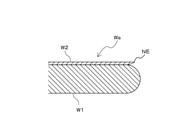
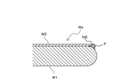
- FIG. 2A is a schematic diagram showing an example of a laminated substrate in which two wafers are bonded.
- FIG. 2B is a schematic view showing a laminated substrate after the second wafer shown in FIG. 2A is thinned.
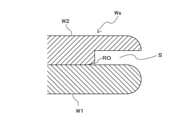
- FIG. 3A is a schematic view showing another example of a laminated substrate in which two wafers are bonded.
- FIG. 3B is a schematic view showing a laminated substrate after the second wafer shown in FIG. 3A is thinned.
- FIG. 4 is a plan view schematically showing the substrate processing apparatus according to the embodiment.
- FIG. 4 is a plan view schematically showing the substrate processing apparatus according to the embodiment.
- FIG. 5 is a vertical sectional view schematically showing the substrate processing apparatus shown in FIG.
- FIG. 6 is a schematic view showing a coating module according to an embodiment.
- FIG. 7 is a schematic diagram showing a curing module according to an embodiment.
- FIG. 8A is a schematic view showing a filler cured in the gap between the peripheral edge portion of the first wafer and the peripheral edge portion of the second wafer of the laminated substrate shown in FIG. 2A.
- FIG. 8B is a schematic view showing a state in which the second wafer of the laminated substrate shown in FIG. 8A is thinned.
- FIG. 9A is a schematic view showing a filler cured in the gap between the peripheral edge portion of the first wafer and the peripheral edge portion of the second wafer of the laminated substrate shown in FIG.
- FIG. 9B is a schematic view showing a state in which the second wafer of the laminated substrate shown in FIG. 9A is thinned.
- FIG. 10 is a schematic view showing a coating module according to another embodiment.
- FIG. 11 is a schematic view showing a coating module according to still another embodiment.
- FIG. 12 is a schematic diagram showing a curing module according to another embodiment.
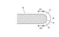
- FIG. 1A and 1B are enlarged cross-sectional views showing a peripheral portion of a wafer which is an example of a substrate. More specifically, FIG. 1A is a cross-sectional view of a so-called straight type wafer, and FIG. 1B is a cross-sectional view of a so-called round type wafer.
- the bevel portion is the outermost peripheral surface of the wafer W composed of an upper inclined portion (upper bevel portion) P, a lower inclined portion (lower bevel portion) Q, and a side portion (apex) R. (Represented by reference numeral B).
- the bevel portion is a portion having a curved cross section (indicated by reference numeral B) constituting the outermost peripheral surface of the wafer W.
- the top edge portion E1 is a region located radially inside the bevel portion B and is a flat portion located radially outside the region D in which the device is formed.
- the top edge portion E1 may include a region in which the device is formed.
- the bottom edge portion E2 is a flat portion located on the opposite side of the top edge portion E1 and radially inside the bevel portion B.
- the top edge portion E1 and the bottom edge portion E2 may be collectively referred to as a near edge portion.
- FIG. 2A is a schematic diagram showing an example of a laminated substrate in which two wafers are bonded
- FIG. 2B is a schematic diagram showing a laminated substrate after the second wafer shown in FIG. 2A is thinned.
- the laminated substrate Ws shown in FIG. 2A is manufactured by joining the round type first wafer W1 and the second wafer W2 shown in FIG. 1B.
- a knife edge portion NE is formed on the peripheral edge portion of the second wafer W2.
- the knife edge portion NE is easily chipped due to physical contact, and may cause the laminated substrate Ws to be cracked or chipped during transportation of the laminated substrate Ws and further process processing of the laminated substrate Ws. Further, if the bonding between the first wafer W1 and the second wafer W2 is not sufficient, the second wafer W2 may be cracked or chipped during the grinding process (that is, the thinning process) of the second wafer W2. .. Even when the laminated substrate Ws is manufactured by joining the square type first wafer W1 and the second wafer W2 shown in FIG. 1A, when the second wafer W2 is thinned, a knife is formed on the peripheral edge of the second wafer W2. An edge portion is formed.
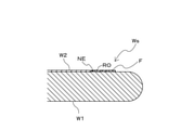
- FIG. 3A is a schematic diagram showing another example of a laminated substrate in which two wafers are bonded
- FIG. 3B is a schematic diagram showing a laminated substrate after the second wafer shown in FIG. 3A is thinned.
- the laminated substrate Ws shown in FIG. 3A is also manufactured by joining the round type first wafer W1 and the second wafer W2 shown in FIG. 1B, and the peripheral edge portion of the second wafer W2 is the second wafer W2. Is polished before being bonded to the first wafer W1. Therefore, a step portion S is formed on the peripheral edge portion of the second wafer W2 over the entire circumference thereof. Further, when the peripheral edge portion of the second wafer W2 is polished to form the step portion S, the roll-off portion RO may be formed on the surface of the second wafer W2 radially inside the step portion S. be.
- this roll-off portion RO can become a knife edge portion NE which is an acute-angled end portion after the second wafer W2 is thinned. Therefore, even if the peripheral edge portion of the second wafer W2 is polished in advance, it is not sufficient to suppress cracking and chipping of the laminated substrate Ws.
- a filler is applied between the first wafer W1 and the second wafer W2 of the laminated substrate Ws, and the filler is cured to effectively protect the knife edge portion NE.
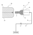
- FIG. 4 is a plan view schematically showing the substrate processing apparatus according to the embodiment
- FIG. 5 is a vertical cross-sectional view schematically showing the substrate processing apparatus shown in FIG.
- the substrate processing apparatus shown in FIGS. 4 and 5 is an apparatus that applies a filler to the gaps formed between the wafers W1 and W2 of the laminated substrate Ws and further cures the filler. Note that FIG. 5 omits the illustration of the coating module 1A and the curing module 1B, which will be described later.
- the substrate processing apparatus 100 horizontally holds a laminated substrate Ws (see FIG. 2A or FIG. 3A) in which a plurality of wafers W1 and W2 are laminated in a central portion thereof, and rotates. It is provided with a rotation holding mechanism (board holding portion) 3 for causing the rotation to be held.
- FIG. 4 shows a state in which the rotation holding mechanism 3 holds the laminated substrate Ws.
- the rotation holding mechanism 3 includes a dish-shaped holding stage 4 that holds the back surface of the laminated substrate Ws by vacuum suction, a hollow shaft 5 connected to the central portion of the holding stage 4, and a motor M1 that rotates the hollow shaft 5. It is equipped with.
- the laminated substrate Ws is placed on the holding stage 4 by a hand (not shown) of the transport mechanism so that the center of the laminated substrate Ws coincides with the axis of the hollow shaft 5.
- the hollow shaft 5 is supported by a ball spline bearing (linear motion bearing) 6 so as to be vertically movable.
- a groove 4a is formed on the upper surface of the holding stage 4, and the groove 4a communicates with a communication passage 7 extending through the hollow shaft 5.
- the communication passage 7 is connected to the vacuum line 9 via a rotary joint 8 attached to the lower end of the hollow shaft 5.
- the communication passage 7 is also connected to a nitrogen gas supply line 10 for separating the treated laminated substrate Ws from the holding stage 4. By switching between these vacuum lines 9 and the nitrogen gas supply line 10, the laminated substrate Ws is vacuum-adsorbed to the upper surface of the holding stage 4 and detached.
- the hollow shaft 5 is rotated by the motor M1 via a pulley p1 connected to the hollow shaft 5, a pulley p2 attached to the rotation shaft of the motor M1, and a belt b1 hung on the pulleys p1 and p2. ..
- the rotation shaft of the motor M1 extends parallel to the hollow shaft 5. With such a configuration, the laminated substrate Ws held on the upper surface of the holding stage 4 is rotated by the motor M1.
- the ball spline bearing 6 is a bearing that allows the hollow shaft 5 to move freely in the longitudinal direction thereof.
- the ball spline bearing 6 is fixed to the cylindrical casing 12. Therefore, in the present embodiment, the hollow shaft 5 is configured to be able to operate linearly up and down with respect to the casing 12, and the hollow shaft 5 and the casing 12 rotate integrally.
- the hollow shaft 5 is connected to an air cylinder (elevating mechanism) 15, and the hollow shaft 5 and the holding stage 4 can be raised and lowered by the air cylinder 15.
- a radial bearing 18 is interposed between the casing 12 and the cylindrical casing 14 arranged concentrically on the outside thereof, and the casing 12 is rotatably supported by the bearing 18.
- the rotation holding mechanism 3 can rotate the laminated substrate Ws around its central axis Cr and raise and lower the laminated substrate Ws along the central axis Cr.
- the substrate processing apparatus 100 includes a coating joule (coating portion) 1A arranged around the laminated substrate Ws held by the rotation holding mechanism 3 and a curing module (curing portion) 1B. ing.
- the curing module 1B is located on the downstream side of the coating module 1B in the rotation direction of the laminated substrate Ws.
- the coating module 1A is a device for applying a filler to the gap between the peripheral edge portion of the first wafer W1 and the peripheral edge portion of the second wafer W2, and the curing module 1B is supplied to the laminated substrate Ws by the coating module 1A. It is a device that cures the filler.
- the filler is a thermosetting filler. Examples of such fillers include thermosetting resins.
- the coating module 1A and the curing module 1B are arranged in the processing chamber 21 partitioned by the partition wall 20, and the processing chamber 21 is separated from the outside by the partition wall 20.
- the coating module 1A, the curing module 1B, and the holding stage 4 are arranged in the processing chamber 21. That is, the laminated substrate Ws being processed is housed in the processing chamber 21.
- FIG. 5 shows a state in which the hollow shaft 5 is lowered, and shows that the holding stage 4 is in the processing position. After the filler is applied and cured, the wafer W is raised to the transfer position together with the holding stage 4 and the hollow shaft 5 by the air cylinder 15, and the wafer W is separated from the holding stage 4 at this transfer position.
- the partition wall 20 is provided with a transport port 20b for loading and unloading the laminated substrate Ws into and out of the processing chamber 21.
- the transport port 20b is formed as a notch extending horizontally. Therefore, the laminated substrate Ws gripped by the transport mechanism can cross the inside of the processing chamber 21 through the transport port 20b while maintaining a horizontal state.
- An opening 20c and a louver 40 are provided on the upper surface of the partition wall 20, and an exhaust port (not shown) is provided on the lower surface.
- the transport port 20b is closed by a shutter (not shown). Therefore, a downflow of clean air is formed inside the processing chamber 21 by exhausting air from the exhaust port by a fan mechanism (not shown). This fan mechanism functions as a pressure adjusting device that keeps the pressure in the processing chamber 21 positive. Since the laminated substrate Ws is processed in this state, the laminated substrate Ws can be processed while keeping the upper space of the processing chamber 21 clean.
- FIG. 6 is a schematic diagram showing a coating module according to an embodiment.
- the coating module 1A shown in FIG. 6 has a syringe mechanism 45 for injecting a filler into a gap between the first wafer W1 and the second wafer W2, and a horizontal moving mechanism for moving the syringe mechanism 45 close to or away from the laminated substrate Ws. (Not shown).
- the horizontal movement mechanism may be omitted.
- the position of the syringe mechanism 45 with respect to the holding stage 4 is predetermined so that the filler can be appropriately injected into the gap between the first wafer W1 and the second wafer W2.
- the syringe mechanism 45 includes a syringe body 46 having a hollow structure and a piston 48 capable of reciprocating in the syringe body 46.
- the syringe body 46 is connected to the gas supply source via the gas supply line 50.
- a gas for example, dry air or nitrogen gas
- the piston 48 advances in the syringe body 46.
- the syringe body 46 has a tip opening facing the gap between the peripheral edge portion of the first wafer W1 and the peripheral edge portion of the second wafer W2.
- the syringe body 46 is pre-filled with the filler F, and by advancing the piston 48, the gap between the peripheral edge of the first wafer W1 and the peripheral edge of the second wafer W2 is formed from the tip opening of the syringe body 46. Filler F is injected.
- a pressure regulator (for example, a pressure reducing valve) 51 and a flow rate regulator (for example, a mass flow controller) 53 are arranged in the gas supply line 50.
- a pressure regulator for example, a pressure reducing valve
- a flow rate regulator for example, a mass flow controller
- the holding stage 4 holding the laminated substrate Ws is rotated at a predetermined rotation speed.
- the syringe mechanism 45 is brought close to the laminated substrate Ws, and gas is further supplied to the syringe body 46 from the gas supply source.
- the filler F is injected into the gap between the peripheral edge portion of the first wafer W1 and the peripheral edge portion of the second wafer W2 of the rotating laminated substrate Ws.
- the filler F injected from the syringe mechanism 45 into the gap between the peripheral edge of the first wafer W1 and the peripheral edge of the second wafer W2 is too large, the filler F overflowing from the gap will be discharged from the laminated substrate Ws. There is a risk of contaminating the top and bottom surfaces. If the amount of filler F injected from the syringe mechanism 45 into the gap between the peripheral edge of the first wafer W1 and the peripheral edge of the second wafer W2 is too small, a sufficient amount of filler F is applied to the gap. May not be possible.
- the necessary and sufficient amount of the filler F is supplied to the gap between the peripheral edge portion of the first wafer W1 and the peripheral edge portion of the second wafer W2 of the rotating laminated substrate Ws.
- the flow rate of the filler F discharged from the syringe body 46 and the rotation speed of the holding stage 4 are adjusted in advance.
- FIG. 7 is a schematic diagram showing a curing module according to an embodiment.
- the curing module 1B shown in FIG. 7 is configured as an optical heating module having a lamp heater 55.
- the lamp heater 55 includes a lamp 83 and an optical device 85 that directs heat (radiant heat) from the lamp 83 to the filler F applied to the gap between the first wafer W1 and the second wafer W2.
- the optical instrument 85 is composed of, for example, a mirror and / or a lens.
- the lamp heater 55 shown in FIG. 7 is arranged above the second wafer W2 of the laminated substrate Ws, and the lamp 83 irradiates light having a wavelength of 1 ⁇ m or more from above the laminated substrate Ws via the optical device 85. ..
- the lamp 83 irradiates light having a wavelength of 1 ⁇ m or more
- the light emitted from the lamp 83 passes through the second wafer W2, so that the peripheral portion of the first wafer W1 and the peripheral portion of the second wafer W2
- the filler F applied to the gap between them can be directly heated.
- the optical heating module having the lamp 83 has high thermal efficiency and can heat and cure the filler F in a short time. Therefore, the throughput of the substrate processing apparatus 100 can be improved.
- the position of the lamp heater 55 with respect to the laminated substrate Ws is arbitrary.
- the lamp heater 55 may be arranged below the first wafer W1. In this case, the light emitted from the lamp 83 passes through the first wafer W1 and directly heats the filler F.
- the lamp heater 55 is arranged so that the lamp 83 faces the gap between the peripheral edge portion of the first wafer W1 and the peripheral edge portion of the second wafer W2. May be good. In this case, the lamp 83 heats the filler F from the side of the laminated substrate Ws. Therefore, since it is not necessary for the light emitted from the lamp 83 to pass through the first wafer W1 or the second wafer W2, any lamp can be used as the lamp 83.
- the laminated substrate Ws is first held by the holding stage 4 of the rotation holding mechanism 3 by vacuum suction. Next, the laminated substrate Ws is rotated together with the holding stage 4. Next, the filler F is applied to the gap between the peripheral edge portion of the first wafer W1 and the peripheral edge portion of the second wafer W2 of the laminated substrate Ws by the coating module 1A, and the filler F is further cured by the curing module 1B. ..
- the coating treatment and the curing treatment of the filler F are continuously performed in the same treatment chamber 21. Therefore, the substrate processing for suppressing the cracking and chipping of the laminated substrate Ws can be performed in a very short time.
- the laminated substrate Ws is carried out from the substrate processing apparatus 100, and the second wafer W2 of the laminated substrate Ws is thinned by another semiconductor manufacturing apparatus.
- FIG. 8A is a schematic view showing a filler cured in the gap between the peripheral edge portion of the first wafer and the peripheral edge portion of the second wafer of the laminated substrate shown in FIG. 2A
- FIG. 8B is a schematic view of the laminated substrate shown in FIG. 8A. It is a schematic diagram which shows the state which the 2nd wafer is thinned. As shown in FIG. 8B, even if the second wafer W2 is thinned, the second wafer W2 is covered with the filler F cured in the gap between the peripheral edge portion of the first wafer W1 and the peripheral edge portion of the second wafer W2. The knife edge portion NE formed on the peripheral portion is protected.
- the peripheral edge portion of the first wafer W1 and the peripheral edge portion of the second wafer W2 are supported by each other via the cured filler F.
- the strength of the laminated substrate Ws is increased, and it is possible to effectively suppress the occurrence of cracking and chipping of the laminated substrate Ws when the second wafer W2 is thinned.
- FIG. 9A is a schematic view showing a filler cured in the gap between the peripheral edge portion of the first wafer and the peripheral edge portion of the second wafer of the laminated substrate shown in FIG. 3A
- FIG. 9B is a schematic view of the laminated substrate shown in FIG. 9A. It is a schematic diagram which shows the state which the 2nd wafer is thinned.
- the filler F is cured in the gap between the peripheral edge portion of the first wafer W1 and the peripheral edge portion of the second wafer W2, including the step portion S and the roll-off portion RO.
- the strength of the laminated substrate Ws is increased, and it is possible to effectively suppress the occurrence of cracking and chipping of the laminated substrate Ws when the second wafer W2 is thinned.
- the filler F protects the knife edge portion NE formed on the peripheral edge portion of the second wafer W2. To. As a result, cracking and chipping of the laminated substrate Ws can be suppressed.
- the coating module 1A has a syringe mechanism 45, but the present embodiment is not limited to this example.
- the configuration of the coating module 1A is arbitrary as long as the filler F can be applied to the gap between the peripheral edge of the first wafer W1 of the laminated substrate Ws and the peripheral edge of W2 of the second wafer.
- FIG. 10 is a schematic diagram showing a coating module according to another embodiment.
- the coating module 1A shown in FIG. 10 has an injection mechanism 60 that ejects the filler F into the gap between the peripheral portion of the first wafer and the peripheral portion of the second wafer of the laminated substrate Ws instead of the syringe mechanism 45. It differs from the coating module 1A shown in FIG. 6 in that it is different from the coating module 1A shown in FIG.
- the injection mechanism 60 shown in FIG. 10 has a tubular injection machine 61 having an injection port 61a.
- the injection port 61a faces the gap between the peripheral edge portion of the first wafer and the peripheral edge portion of the second wafer of the laminated substrate Ws.
- the injection machine 61 has a filler F filled therein in advance, and is connected to the gas supply source via the gas supply line 50.
- a gas for example, dry air or nitrogen gas
- the filler F is formed in the gap between the peripheral edge of the first wafer W1 and the peripheral edge of the second wafer W2 from the injection port 61a. Is continuously ejected.
- the injection machine 61 may be a piston cylinder device.
- the gas supplied from the gas supply source to the injection machine 61 causes the piston to move forward in the cylinder, and the filler F filled in the cylinder is continuously injected from the injection port 61a.
- a pressure regulator (for example, a pressure reducing valve) 51 and a flow rate regulator (for example, a mass flow controller) 53 are arranged in the gas supply line 50.
- a pressure regulator for example, a pressure reducing valve
- a flow rate regulator for example, a mass flow controller
- the injection port is provided so that a necessary and sufficient amount of the filler F is supplied to the gap between the peripheral edge portion of the first wafer W1 and the peripheral edge portion of the second wafer W2 of the rotating laminated substrate Ws.
- the flow rate of the filler F ejected from 61a and the rotation speed of the holding stage 4 are adjusted in advance.
- FIG. 11 is a schematic diagram showing a coating module according to still another embodiment.
- the coating module 1A shown in FIG. 11 differs from the coating module 1A shown in FIG. 6 in that it has a carrier 65 for the filler F instead of the syringe mechanism 45.
- the transport mechanism 65 shown in FIG. 11 includes a tube 66 having a discharge port 66a and a filler transport member 68 connected to the discharge port 66a.
- the filler transport member 68 is a rod-shaped member extending diagonally downward from the lower end of the discharge port 66a, and the tip of the filler transport member 68 is a peripheral portion of the first wafer W1 and the second wafer W2 of the laminated substrate Ws. Close to or in contact with the gap between the edges.
- the filler transport member 68 is formed of a hydrophilic material. In one embodiment, the surface of the filler transport member 68 may be subjected to a hydrophilic treatment such as coating of a hydrophilic material.
- the filler transport member 68 has a thickness that can be inserted into the gap between the peripheral edge portion of the first wafer W1 and the peripheral edge portion of the second wafer W2, for example.
- the filler transport member 68 preferably has flexibility so as not to damage the laminated substrate Ws.
- the tube 66 has a filler F filled therein in advance, and is connected to a gas supply source via a gas supply line 50.
- a gas for example, dry air or nitrogen gas
- the filler F flows out from the discharge port 66a and flows on the surface of the filler transport member 68. Since the tip of the filler transport member 68 is close to or in contact with the gap between the peripheral edge portion of the first wafer W1 and the peripheral edge portion of the second wafer W2, the filler F is transferred to the filler transport member. It can be conveyed to the gap between the peripheral edge portion of the first wafer W1 and the peripheral edge portion of the second wafer W2 via 68.
- the tube 66 is provided so that a necessary and sufficient amount of filler F is supplied to the gap between the peripheral edge portion of the first wafer W1 and the peripheral edge portion of the second wafer W2 of the rotating laminated substrate Ws.
- the flow rate of the filler F flowing out of the filler F and the rotation speed of the holding stage 4 are adjusted in advance. According to such a configuration, the amount of the filler F supplied to the gap between the peripheral edge portion of the first wafer W1 and the peripheral edge portion of the second wafer W2 can be controlled more precisely.
- the transport mechanism 65 may have a piston cylinder device instead of the tube 66.
- the filler transport member 68 is connected to the tip opening of the cylinder of the piston cylinder device.
- the curing module 1B is configured as a light heating module having a lamp 83, but the present embodiment is not limited to this example.
- the configuration of the coating module 1B is arbitrary as long as it is possible to cure the filler F applied to the gap between the peripheral portion of the first wafer W1 of the laminated substrate Ws and the peripheral portion of W2 of the second wafer.
- FIG. 12 is a schematic diagram showing a curing module according to another embodiment.
- the curing module 1B shown in FIG. 12 is a heat gun that blows hot air toward the filler F applied to the gap between the peripheral edge portion of the first wafer W1 and the peripheral edge portion of the second wafer W2 instead of the lamp heater 55. It differs from the curing module 1B shown in FIG. 7 in that it has 87.
- the heat gun 87 shown in FIG. 12 has an injection port 87a facing the filler F applied to the gap between the peripheral edge portion of the first wafer W1 and the peripheral edge portion of the W2 of the second wafer of the laminated substrate Ws. Further, the heat gun 87 has a heater (not shown) arranged inside the heat gun 87, and a fan device (not shown) that sends the gas heated by the heater toward the injection port 87a. The heat gun 87 cures the filler F while pressing the filler F toward the center of the laminated substrate Ws by the hot air ejected from the injection port 87a.
- the filler F applied to the gap between the peripheral edge portion of the first wafer W1 and the peripheral edge portion of the second wafer W2 of the laminated substrate Ws. Can be instantly heated and cured.
- the filler F may evaporate rapidly and voids may be formed in the filler F after curing.
- the heat gun 87 is configured so that the amount of hot air blown from the injection port 87a and the temperature of the hot air can be adjusted. Therefore, the heat gun 87 can heat the filler F more slowly than the light heating of the lamp 83, and can appropriately press the filler F toward the center of the laminated substrate Ws by hot air. By this action of the heat gun 87, it is possible to effectively suppress the formation of voids in the filler F after curing.
- the present invention can be used as a substrate processing method for suppressing cracking and chipping of a laminated substrate manufactured by joining a plurality of substrates. Further, the present invention can be used for a substrate processing apparatus capable of carrying out such a substrate processing method.
Landscapes
- Container, Conveyance, Adherence, Positioning, Of Wafer (AREA)
- Health & Medical Sciences (AREA)
- Toxicology (AREA)
- Mechanical Treatment Of Semiconductor (AREA)
- Production Of Multi-Layered Print Wiring Board (AREA)
- Application Of Or Painting With Fluid Materials (AREA)
- Coating Apparatus (AREA)
Abstract
Description
また、本発明は、上記方法を実施可能な基板処理装置を提供することを目的とする。
一態様では、前記充填剤を塗布する工程は、射出機構を用いて前記充填剤を前記隙間に射出する工程であり、前記射出機構は、前記充填剤が充填された射出機を有し、前記射出機は、前記隙間に対向する射出口を有する。
一態様では、前記充填剤を塗布する工程は、搬送機構を用いて前記充填剤を前記隙間に搬送する工程であり、前記搬送機構は、吐出口を有し、充填剤が充填されたチューブと、前記吐出口から延びて、前記隙間に近接するか、または接触する充填剤搬送部材と、を有する。
一態様では、前記ランプヒータは、1μm以上の波長を有する光を、前記積層基板の上方または下方から前記充填剤に向けて照射させる。
一態様では、前記充填剤を硬化させる工程は、ヒートガンによって前記充填剤を硬化させる工程である。
一態様では、前記塗布モジュールは、射出機構を備えており、前記射出機構は、前記充填剤が充填された射出機を有し、前記射出機は、前記隙間に対向する射出口を有する。
一態様では、前記塗布モジュールは、搬送機構を備えており、前記搬送機構は、吐出口を有し、充填剤が充填されたチューブと、前記吐出口から延びて、前記隙間に近接するか、または接触する充填剤搬送部材と、を有する。
一態様では、前記ランプは、1μm以上の波長を有する光を発するように構成されており、前記ランプヒータは、前記積層基板の上方または下方に配置される。
一態様では、前記硬化モジュールは、前記充填剤に向けて熱風を吹き付けるヒートガンを備える。
図1Aおよび図1Bは、基板の一例であるウエハの周縁部を示す拡大断面図である。より詳しくは、図1Aはいわゆるストレート型のウエハの断面図であり、図1Bはいわゆるラウンド型のウエハの断面図である。図1AのウエハWにおいて、ベベル部は、上側傾斜部(上側ベベル部)P、下側傾斜部(下側ベベル部)Q、および側部(アペックス)Rから構成されるウエハWの最外周面(符号Bで示す)である。
1B 硬化モジュール
3 回転保持機構(基板保持部)
4 保持ステージ
20 隔壁
21 処理室
45 シリンジ機構
46 シリンジ本体
48 ピストン
50 気体供給ライン
51 圧力調整装置
53 流量調整装置
55 ランプヒータ
60 射出機構
61 射出機
65 搬送機構
66 チューブ
68 充填剤搬送部材
83 ランプ
85 光学機器
87 ヒートガン
100 基板処理装置
Claims (14)
- 第1基板と第2基板を接合して製造される積層基板を回転させ、
前記第1基板の周縁部と、前記第2基板の周縁部との間の隙間に熱硬化性を有する充填剤を塗布し、
前記充填剤を硬化させ、
前記充填剤を塗布する工程と、前記充填剤を硬化させる工程は、同一の処理室内で連続して行われる、基板処理方法。 - 前記充填剤を塗布する工程は、シリンジ機構を用いて前記充填剤を前記隙間に注入する工程であり、
前記シリンジ機構は、
前記充填剤が充填されたシリンジ本体と、
前記シリンジ本体内を移動可能なピストンと、を有し、
前記シリンジ本体の先端開口は、前記隙間に対向している、請求項1に記載の基板処理方法。 - 前記充填剤を塗布する工程は、射出機構を用いて前記充填剤を前記隙間に射出する工程であり、
前記射出機構は、前記充填剤が充填された射出機を有し、
前記射出機は、前記隙間に対向する射出口を有する、請求項1に記載の基板処理方法。 - 前記充填剤を塗布する工程は、搬送機構を用いて前記充填剤を前記隙間に搬送する工程であり、
前記搬送機構は、
吐出口を有し、充填剤が充填されたチューブと、
前記吐出口から延びて、前記隙間に近接するか、または接触する充填剤搬送部材と、を有する、請求項1に記載の基板処理方法。 - 前記充填剤を硬化させる工程は、ランプヒータによって前記充填剤を硬化させる工程である、請求項1乃至4のいずれか一項に記載の基板処理方法。
- 前記ランプヒータは、1μm以上の波長を有する光を、前記積層基板の上方または下方から前記充填剤に向けて照射させる、請求項5に記載の基板処理方法。
- 前記充填剤を硬化させる工程は、ヒートガンによって前記充填剤を硬化させる工程である、請求項1乃至4のいずれか一項に記載の基板処理方法。
- 第1基板と第2基板を接合して製造される積層基板を保持し、回転させる基板保持部と、
前記第1基板の周縁部と、前記第2基板の周縁部との間の隙間に熱硬化性を有する充填剤を塗布する塗布モジュールと、
前記充填剤を硬化させる硬化モジュールと、
前記基板保持部、前記塗布モジュール、および前記硬化モジュールが配置された処理室と、を備え、
前記充填剤の塗布および硬化は、前記処理室内で前記積層基板を回転させながら連続して行われる、基板処理装置。 - 前記塗布モジュールは、シリンジ機構を備えており、
前記シリンジ機構は、
前記充填剤が充填されたシリンジ本体と、
前記シリンジ本体内を移動可能なピストンと、を有し、
前記シリンジ本体の先端開口は、前記隙間に対向している、請求項8に記載の基板処理装置。 - 前記塗布モジュールは、射出機構を備えており、
前記射出機構は、前記充填剤が充填された射出機を有し、
前記射出機は、前記隙間に対向する射出口を有する、請求項8に記載の基板処理装置。 - 前記塗布モジュールは、搬送機構を備えており、
前記搬送機構は、
吐出口を有し、充填剤が充填されたチューブと、
前記吐出口から延びて、前記隙間に近接するか、または接触する充填剤搬送部材と、を有する、請求項8に記載の基板処理装置。 - 前記硬化モジュールは、ランプヒータを備えており、
前記ランプヒータは、
ランプと、
前記ランプからの熱を、前記隙間に塗布された充填剤に向ける光学機器と、を有している、請求項8乃至11のいずれか一項に記載の基板処理装置。 - 前記ランプは、1μm以上の波長を有する光を発するように構成されており、
前記ランプヒータは、前記積層基板の上方または下方に配置される、請求項12に記載の基板処理装置。 - 前記硬化モジュールは、前記充填剤に向けて熱風を吹き付けるヒートガンを備える、請求項8乃至11のいずれか一項に記載の基板処理装置。
Priority Applications (4)
| Application Number | Priority Date | Filing Date | Title |
|---|---|---|---|
| KR1020237009330A KR20230054415A (ko) | 2020-08-27 | 2021-06-25 | 기판 처리 방법 및 기판 처리 장치 |
| US18/041,256 US20230326757A1 (en) | 2020-08-27 | 2021-06-25 | Substrate processing method and substrate processing apparatus |
| CN202180052111.5A CN115885367A (zh) | 2020-08-27 | 2021-06-25 | 基板处理方法及基板处理装置 |
| EP21860952.7A EP4207246A4 (en) | 2020-08-27 | 2021-06-25 | SUBSTRATE PROCESSING METHOD AND SUBSTRATE PROCESSING DEVICE |
Applications Claiming Priority (2)
| Application Number | Priority Date | Filing Date | Title |
|---|---|---|---|
| JP2020-143517 | 2020-08-27 | ||
| JP2020143517A JP7535891B2 (ja) | 2020-08-27 | 2020-08-27 | 基板処理方法、および基板処理装置 |
Publications (1)
| Publication Number | Publication Date |
|---|---|
| WO2022044522A1 true WO2022044522A1 (ja) | 2022-03-03 |
Family
ID=80354907
Family Applications (1)
| Application Number | Title | Priority Date | Filing Date |
|---|---|---|---|
| PCT/JP2021/024080 Ceased WO2022044522A1 (ja) | 2020-08-27 | 2021-06-25 | 基板処理方法、および基板処理装置 |
Country Status (7)
| Country | Link |
|---|---|
| US (1) | US20230326757A1 (ja) |
| EP (1) | EP4207246A4 (ja) |
| JP (1) | JP7535891B2 (ja) |
| KR (1) | KR20230054415A (ja) |
| CN (1) | CN115885367A (ja) |
| TW (1) | TWI894340B (ja) |
| WO (1) | WO2022044522A1 (ja) |
Families Citing this family (8)
| Publication number | Priority date | Publication date | Assignee | Title |
|---|---|---|---|---|
| JP2024010745A (ja) * | 2022-07-13 | 2024-01-25 | 株式会社荏原製作所 | 基板製造方法および基板製造装置 |
| JP2024010749A (ja) | 2022-07-13 | 2024-01-25 | 株式会社荏原製作所 | 基板保持装置、基板製造装置、および基板製造方法 |
| JP2024022110A (ja) * | 2022-08-05 | 2024-02-16 | 株式会社荏原製作所 | 充填剤塗布装置 |
| JP2024060666A (ja) * | 2022-10-20 | 2024-05-07 | 株式会社荏原製作所 | 基板処理装置および基板処理方法 |
| JP2024090377A (ja) * | 2022-12-23 | 2024-07-04 | 株式会社荏原製作所 | 積層構造体製造装置および積層構造体の製造方法 |
| JP2024111881A (ja) * | 2023-02-07 | 2024-08-20 | 株式会社荏原製作所 | 基板処理装置 |
| JP2025115434A (ja) * | 2024-01-26 | 2025-08-07 | 株式会社荏原製作所 | 基板処理装置および基板処理方法 |
| US20260011607A1 (en) * | 2024-07-03 | 2026-01-08 | Applied Materials, Inc. | Substrate for Semiconductor Fabrication Having Selectively Treated Perimeter and Method of Treating |
Citations (3)
| Publication number | Priority date | Publication date | Assignee | Title |
|---|---|---|---|---|
| JP2006352078A (ja) * | 2005-05-16 | 2006-12-28 | Fuji Electric Holdings Co Ltd | 半導体装置の製造方法 |
| JP2014063955A (ja) | 2012-09-24 | 2014-04-10 | Ebara Corp | 研磨方法 |
| JP2014167966A (ja) * | 2013-02-28 | 2014-09-11 | Toshiba Corp | 半導体装置の製造方法及び製造装置 |
Family Cites Families (12)
| Publication number | Priority date | Publication date | Assignee | Title |
|---|---|---|---|---|
| NL6816121A (ja) * | 1968-11-12 | 1970-05-14 | ||
| JP4313874B2 (ja) * | 1999-02-02 | 2009-08-12 | キヤノン株式会社 | 基板の製造方法 |
| CN101327572B (zh) * | 2007-06-22 | 2012-01-25 | 中芯国际集成电路制造(上海)有限公司 | 晶圆背面减薄工艺 |
| US9111981B2 (en) * | 2008-01-24 | 2015-08-18 | Brewer Science Inc. | Method for reversibly mounting a device wafer to a carrier substrate |
| JP3142547U (ja) * | 2008-03-10 | 2008-06-19 | 稔 中村 | 液体吐出用シリンジ |
| EP2315663B1 (en) * | 2008-08-12 | 2020-09-23 | 3M Innovative Properties Company | Adhesives compatible with corrosion sensitive layers |
| WO2011014446A1 (en) * | 2009-07-31 | 2011-02-03 | Nantero, Inc. | Anisotropic nanotube fabric layers and films and methods of forming same |
| FR2983346B1 (fr) * | 2011-11-25 | 2016-12-09 | Soitec Silicon On Insulator | Procede de prevention d'une panne electrique dans un empilement de couches semi-conductrices, cellule photovoltaïque a concentration a substrat mince, et assemblage de cellule solaire |
| US9157014B2 (en) * | 2012-11-29 | 2015-10-13 | Micron Technology, Inc. | Adhesives including a filler material and related methods |
| US10067499B2 (en) * | 2015-03-13 | 2018-09-04 | Arevo, Inc. | System and method for additive manufacturing of thermoset polymers |
| KR102508077B1 (ko) * | 2015-06-09 | 2023-03-10 | 루미리즈 홀딩 비.브이. | 고굴절률 접착제들을 이용한 led 제조 |
| JP6635860B2 (ja) * | 2016-04-07 | 2020-01-29 | 株式会社ディスコ | 加工方法 |
-
2020
- 2020-08-27 JP JP2020143517A patent/JP7535891B2/ja active Active
-
2021
- 2021-06-25 KR KR1020237009330A patent/KR20230054415A/ko active Pending
- 2021-06-25 EP EP21860952.7A patent/EP4207246A4/en active Pending
- 2021-06-25 CN CN202180052111.5A patent/CN115885367A/zh active Pending
- 2021-06-25 US US18/041,256 patent/US20230326757A1/en active Pending
- 2021-06-25 WO PCT/JP2021/024080 patent/WO2022044522A1/ja not_active Ceased
- 2021-08-24 TW TW110131224A patent/TWI894340B/zh active
Patent Citations (3)
| Publication number | Priority date | Publication date | Assignee | Title |
|---|---|---|---|---|
| JP2006352078A (ja) * | 2005-05-16 | 2006-12-28 | Fuji Electric Holdings Co Ltd | 半導体装置の製造方法 |
| JP2014063955A (ja) | 2012-09-24 | 2014-04-10 | Ebara Corp | 研磨方法 |
| JP2014167966A (ja) * | 2013-02-28 | 2014-09-11 | Toshiba Corp | 半導体装置の製造方法及び製造装置 |
Non-Patent Citations (1)
| Title |
|---|
| See also references of EP4207246A4 |
Also Published As
| Publication number | Publication date |
|---|---|
| CN115885367A (zh) | 2023-03-31 |
| EP4207246A1 (en) | 2023-07-05 |
| US20230326757A1 (en) | 2023-10-12 |
| KR20230054415A (ko) | 2023-04-24 |
| JP7535891B2 (ja) | 2024-08-19 |
| TWI894340B (zh) | 2025-08-21 |
| TW202226336A (zh) | 2022-07-01 |
| EP4207246A4 (en) | 2024-11-06 |
| JP2022038834A (ja) | 2022-03-10 |
Similar Documents
| Publication | Publication Date | Title |
|---|---|---|
| WO2022044522A1 (ja) | 基板処理方法、および基板処理装置 | |
| KR102760744B1 (ko) | 기판 처리 시스템 및 기판 처리 방법 | |
| JP7289579B2 (ja) | チップ接合システムおよびチップ接合方法 | |
| US10658204B2 (en) | Spin chuck with concentrated center and radial heating | |
| JP6277021B2 (ja) | ウエーハ処理装置及びウエーハの処理方法 | |
| KR20240049338A (ko) | 기판 처리 방법 및 기판 처리 장치 | |
| CN110609447A (zh) | 涂布膜形成方法和涂布膜形成装置 | |
| JP7521978B2 (ja) | 保護部材形成装置 | |
| WO2023042547A1 (ja) | 基板処理装置、および基板処理方法 | |
| JP2005064234A (ja) | プラズマエッチング方法及びプラズマエッチング装置 | |
| JP6401988B2 (ja) | 加工装置及びウエーハの加工方法 | |
| JP2016157718A (ja) | ウエーハの搬送方法及びウエーハの搬送機構 | |
| CN117157740A (zh) | 晶圆的制造方法 | |
| US12544994B2 (en) | Substrate processing method | |
| JP2022017700A (ja) | 基板処理方法、および基板処理装置 | |
| JP2023042561A (ja) | 基板処理装置、および基板処理方法 | |
| JP7830209B2 (ja) | 搬送パッド | |
| CN119631165A (zh) | 填充剂涂布装置 | |
| US20250014889A1 (en) | Processing method of wafer | |
| CN117957639A (zh) | 基板处理装置及基板处理方法 | |
| KR20040025841A (ko) | 기판처리장치, 기판처리방법, 도포방법 및 도포장치 | |
| US20240136193A1 (en) | Method of processing wafer | |
| CN117916859A (zh) | 基板处理方法 | |
| WO2024014223A1 (ja) | 基板保持装置、基板製造装置、および基板製造方法 | |
| JP2024062297A (ja) | ウエーハの加工方法 |
Legal Events
| Date | Code | Title | Description |
|---|---|---|---|
| 121 | Ep: the epo has been informed by wipo that ep was designated in this application |
Ref document number: 21860952 Country of ref document: EP Kind code of ref document: A1 |
|
| ENP | Entry into the national phase |
Ref document number: 20237009330 Country of ref document: KR Kind code of ref document: A |
|
| NENP | Non-entry into the national phase |
Ref country code: DE |
|
| ENP | Entry into the national phase |
Ref document number: 2021860952 Country of ref document: EP Effective date: 20230327 |
|
| WWG | Wipo information: grant in national office |
Ref document number: 11202300964S Country of ref document: SG |
|
| WWP | Wipo information: published in national office |
Ref document number: 11202300964S Country of ref document: SG |