WO2022054155A1 - 電力変換装置及び電力変換装置を搭載した航空機 - Google Patents
電力変換装置及び電力変換装置を搭載した航空機 Download PDFInfo
- Publication number
- WO2022054155A1 WO2022054155A1 PCT/JP2020/034055 JP2020034055W WO2022054155A1 WO 2022054155 A1 WO2022054155 A1 WO 2022054155A1 JP 2020034055 W JP2020034055 W JP 2020034055W WO 2022054155 A1 WO2022054155 A1 WO 2022054155A1
- Authority
- WO
- WIPO (PCT)
- Prior art keywords
- voltage
- phase
- semiconductor
- switching element
- inverter
- Prior art date
- Legal status (The legal status is an assumption and is not a legal conclusion. Google has not performed a legal analysis and makes no representation as to the accuracy of the status listed.)
- Ceased
Links
Images





Classifications
-
- H—ELECTRICITY
- H02—GENERATION; CONVERSION OR DISTRIBUTION OF ELECTRIC POWER
- H02M—APPARATUS FOR CONVERSION BETWEEN AC AND AC, BETWEEN AC AND DC, OR BETWEEN DC AND DC, AND FOR USE WITH MAINS OR SIMILAR POWER SUPPLY SYSTEMS; CONVERSION OF DC OR AC INPUT POWER INTO SURGE OUTPUT POWER; CONTROL OR REGULATION THEREOF
- H02M1/00—Details of apparatus for conversion
- H02M1/0095—Hybrid converter topologies, e.g. NPC mixed with flying capacitor, thyristor converter mixed with MMC or charge pump mixed with buck
-
- B—PERFORMING OPERATIONS; TRANSPORTING
- B60—VEHICLES IN GENERAL
- B60L—PROPULSION OF ELECTRICALLY-PROPELLED VEHICLES; SUPPLYING ELECTRIC POWER FOR AUXILIARY EQUIPMENT OF ELECTRICALLY-PROPELLED VEHICLES; ELECTRODYNAMIC BRAKE SYSTEMS FOR VEHICLES IN GENERAL; MAGNETIC SUSPENSION OR LEVITATION FOR VEHICLES; MONITORING OPERATING VARIABLES OF ELECTRICALLY-PROPELLED VEHICLES; ELECTRIC SAFETY DEVICES FOR ELECTRICALLY-PROPELLED VEHICLES
- B60L3/00—Electric devices on electrically-propelled vehicles for safety purposes; Monitoring operating variables, e.g. speed, deceleration or energy consumption
- B60L3/0023—Detecting, eliminating, remedying or compensating for drive train abnormalities, e.g. failures within the drive train
- B60L3/003—Detecting, eliminating, remedying or compensating for drive train abnormalities, e.g. failures within the drive train relating to inverters
-
- B—PERFORMING OPERATIONS; TRANSPORTING
- B60—VEHICLES IN GENERAL
- B60L—PROPULSION OF ELECTRICALLY-PROPELLED VEHICLES; SUPPLYING ELECTRIC POWER FOR AUXILIARY EQUIPMENT OF ELECTRICALLY-PROPELLED VEHICLES; ELECTRODYNAMIC BRAKE SYSTEMS FOR VEHICLES IN GENERAL; MAGNETIC SUSPENSION OR LEVITATION FOR VEHICLES; MONITORING OPERATING VARIABLES OF ELECTRICALLY-PROPELLED VEHICLES; ELECTRIC SAFETY DEVICES FOR ELECTRICALLY-PROPELLED VEHICLES
- B60L3/00—Electric devices on electrically-propelled vehicles for safety purposes; Monitoring operating variables, e.g. speed, deceleration or energy consumption
- B60L3/12—Recording operating variables ; Monitoring of operating variables
-
- B—PERFORMING OPERATIONS; TRANSPORTING
- B60—VEHICLES IN GENERAL
- B60L—PROPULSION OF ELECTRICALLY-PROPELLED VEHICLES; SUPPLYING ELECTRIC POWER FOR AUXILIARY EQUIPMENT OF ELECTRICALLY-PROPELLED VEHICLES; ELECTRODYNAMIC BRAKE SYSTEMS FOR VEHICLES IN GENERAL; MAGNETIC SUSPENSION OR LEVITATION FOR VEHICLES; MONITORING OPERATING VARIABLES OF ELECTRICALLY-PROPELLED VEHICLES; ELECTRIC SAFETY DEVICES FOR ELECTRICALLY-PROPELLED VEHICLES
- B60L53/00—Methods of charging batteries, specially adapted for electric vehicles; Charging stations or on-board charging equipment therefor; Exchange of energy storage elements in electric vehicles
- B60L53/20—Methods of charging batteries, specially adapted for electric vehicles; Charging stations or on-board charging equipment therefor; Exchange of energy storage elements in electric vehicles characterised by converters located in the vehicle
-
- B—PERFORMING OPERATIONS; TRANSPORTING
- B64—AIRCRAFT; AVIATION; COSMONAUTICS
- B64D—EQUIPMENT FOR FITTING IN OR TO AIRCRAFT; FLIGHT SUITS; PARACHUTES; ARRANGEMENT OR MOUNTING OF POWER PLANTS OR PROPULSION TRANSMISSIONS IN AIRCRAFT
- B64D47/00—Equipment not otherwise provided for
-
- H—ELECTRICITY
- H02—GENERATION; CONVERSION OR DISTRIBUTION OF ELECTRIC POWER
- H02M—APPARATUS FOR CONVERSION BETWEEN AC AND AC, BETWEEN AC AND DC, OR BETWEEN DC AND DC, AND FOR USE WITH MAINS OR SIMILAR POWER SUPPLY SYSTEMS; CONVERSION OF DC OR AC INPUT POWER INTO SURGE OUTPUT POWER; CONTROL OR REGULATION THEREOF
- H02M1/00—Details of apparatus for conversion
- H02M1/32—Means for protecting converters other than automatic disconnection
-
- H—ELECTRICITY
- H02—GENERATION; CONVERSION OR DISTRIBUTION OF ELECTRIC POWER
- H02M—APPARATUS FOR CONVERSION BETWEEN AC AND AC, BETWEEN AC AND DC, OR BETWEEN DC AND DC, AND FOR USE WITH MAINS OR SIMILAR POWER SUPPLY SYSTEMS; CONVERSION OF DC OR AC INPUT POWER INTO SURGE OUTPUT POWER; CONTROL OR REGULATION THEREOF
- H02M7/00—Conversion of AC power input into DC power output; Conversion of DC power input into AC power output
- H02M7/42—Conversion of DC power input into AC power output without possibility of reversal
- H02M7/44—Conversion of DC power input into AC power output without possibility of reversal by static converters
- H02M7/48—Conversion of DC power input into AC power output without possibility of reversal by static converters using discharge tubes with control electrode or semiconductor devices with control electrode
- H02M7/53—Conversion of DC power input into AC power output without possibility of reversal by static converters using discharge tubes with control electrode or semiconductor devices with control electrode using devices of a triode or transistor type requiring continuous application of a control signal
- H02M7/537—Conversion of DC power input into AC power output without possibility of reversal by static converters using discharge tubes with control electrode or semiconductor devices with control electrode using devices of a triode or transistor type requiring continuous application of a control signal using semiconductor devices only, e.g. single switched pulse inverters
- H02M7/5387—Conversion of DC power input into AC power output without possibility of reversal by static converters using discharge tubes with control electrode or semiconductor devices with control electrode using devices of a triode or transistor type requiring continuous application of a control signal using semiconductor devices only, e.g. single switched pulse inverters in a bridge configuration
- H02M7/53871—Conversion of DC power input into AC power output without possibility of reversal by static converters using discharge tubes with control electrode or semiconductor devices with control electrode using devices of a triode or transistor type requiring continuous application of a control signal using semiconductor devices only, e.g. single switched pulse inverters in a bridge configuration with automatic control of output voltage or current
-
- B—PERFORMING OPERATIONS; TRANSPORTING
- B60—VEHICLES IN GENERAL
- B60L—PROPULSION OF ELECTRICALLY-PROPELLED VEHICLES; SUPPLYING ELECTRIC POWER FOR AUXILIARY EQUIPMENT OF ELECTRICALLY-PROPELLED VEHICLES; ELECTRODYNAMIC BRAKE SYSTEMS FOR VEHICLES IN GENERAL; MAGNETIC SUSPENSION OR LEVITATION FOR VEHICLES; MONITORING OPERATING VARIABLES OF ELECTRICALLY-PROPELLED VEHICLES; ELECTRIC SAFETY DEVICES FOR ELECTRICALLY-PROPELLED VEHICLES
- B60L2200/00—Type of vehicles
- B60L2200/10—Air crafts
-
- B—PERFORMING OPERATIONS; TRANSPORTING
- B60—VEHICLES IN GENERAL
- B60L—PROPULSION OF ELECTRICALLY-PROPELLED VEHICLES; SUPPLYING ELECTRIC POWER FOR AUXILIARY EQUIPMENT OF ELECTRICALLY-PROPELLED VEHICLES; ELECTRODYNAMIC BRAKE SYSTEMS FOR VEHICLES IN GENERAL; MAGNETIC SUSPENSION OR LEVITATION FOR VEHICLES; MONITORING OPERATING VARIABLES OF ELECTRICALLY-PROPELLED VEHICLES; ELECTRIC SAFETY DEVICES FOR ELECTRICALLY-PROPELLED VEHICLES
- B60L2210/00—Converter types
- B60L2210/40—DC to AC converters
-
- B—PERFORMING OPERATIONS; TRANSPORTING
- B64—AIRCRAFT; AVIATION; COSMONAUTICS
- B64D—EQUIPMENT FOR FITTING IN OR TO AIRCRAFT; FLIGHT SUITS; PARACHUTES; ARRANGEMENT OR MOUNTING OF POWER PLANTS OR PROPULSION TRANSMISSIONS IN AIRCRAFT
- B64D2221/00—Electric power distribution systems onboard aircraft
-
- B—PERFORMING OPERATIONS; TRANSPORTING
- B64—AIRCRAFT; AVIATION; COSMONAUTICS
- B64D—EQUIPMENT FOR FITTING IN OR TO AIRCRAFT; FLIGHT SUITS; PARACHUTES; ARRANGEMENT OR MOUNTING OF POWER PLANTS OR PROPULSION TRANSMISSIONS IN AIRCRAFT
- B64D27/00—Arrangement or mounting of power plants in aircraft; Aircraft characterised by the type or position of power plants
- B64D27/02—Aircraft characterised by the type or position of power plants
- B64D27/30—Aircraft characterised by electric power plants
- B64D27/35—Arrangements for on-board electric energy production, distribution, recovery or storage
- B64D27/359—Arrangements for on-board electric energy production, distribution, recovery or storage using capacitors
-
- H—ELECTRICITY
- H02—GENERATION; CONVERSION OR DISTRIBUTION OF ELECTRIC POWER
- H02M—APPARATUS FOR CONVERSION BETWEEN AC AND AC, BETWEEN AC AND DC, OR BETWEEN DC AND DC, AND FOR USE WITH MAINS OR SIMILAR POWER SUPPLY SYSTEMS; CONVERSION OF DC OR AC INPUT POWER INTO SURGE OUTPUT POWER; CONTROL OR REGULATION THEREOF
- H02M7/00—Conversion of AC power input into DC power output; Conversion of DC power input into AC power output
- H02M7/42—Conversion of DC power input into AC power output without possibility of reversal
- H02M7/44—Conversion of DC power input into AC power output without possibility of reversal by static converters
- H02M7/48—Conversion of DC power input into AC power output without possibility of reversal by static converters using discharge tubes with control electrode or semiconductor devices with control electrode
- H02M7/483—Converters with outputs that each can have more than two voltages levels
- H02M7/4835—Converters with outputs that each can have more than two voltages levels comprising two or more cells, each including a switchable capacitor, the capacitors having a nominal charge voltage which corresponds to a given fraction of the input voltage, and the capacitors being selectively connected in series to determine the instantaneous output voltage
-
- H—ELECTRICITY
- H02—GENERATION; CONVERSION OR DISTRIBUTION OF ELECTRIC POWER
- H02M—APPARATUS FOR CONVERSION BETWEEN AC AND AC, BETWEEN AC AND DC, OR BETWEEN DC AND DC, AND FOR USE WITH MAINS OR SIMILAR POWER SUPPLY SYSTEMS; CONVERSION OF DC OR AC INPUT POWER INTO SURGE OUTPUT POWER; CONTROL OR REGULATION THEREOF
- H02M7/00—Conversion of AC power input into DC power output; Conversion of DC power input into AC power output
- H02M7/42—Conversion of DC power input into AC power output without possibility of reversal
- H02M7/44—Conversion of DC power input into AC power output without possibility of reversal by static converters
- H02M7/48—Conversion of DC power input into AC power output without possibility of reversal by static converters using discharge tubes with control electrode or semiconductor devices with control electrode
- H02M7/483—Converters with outputs that each can have more than two voltages levels
- H02M7/487—Neutral point clamped inverters
-
- H—ELECTRICITY
- H02—GENERATION; CONVERSION OR DISTRIBUTION OF ELECTRIC POWER
- H02M—APPARATUS FOR CONVERSION BETWEEN AC AND AC, BETWEEN AC AND DC, OR BETWEEN DC AND DC, AND FOR USE WITH MAINS OR SIMILAR POWER SUPPLY SYSTEMS; CONVERSION OF DC OR AC INPUT POWER INTO SURGE OUTPUT POWER; CONTROL OR REGULATION THEREOF
- H02M7/00—Conversion of AC power input into DC power output; Conversion of DC power input into AC power output
- H02M7/42—Conversion of DC power input into AC power output without possibility of reversal
- H02M7/44—Conversion of DC power input into AC power output without possibility of reversal by static converters
- H02M7/48—Conversion of DC power input into AC power output without possibility of reversal by static converters using discharge tubes with control electrode or semiconductor devices with control electrode
- H02M7/53—Conversion of DC power input into AC power output without possibility of reversal by static converters using discharge tubes with control electrode or semiconductor devices with control electrode using devices of a triode or transistor type requiring continuous application of a control signal
- H02M7/537—Conversion of DC power input into AC power output without possibility of reversal by static converters using discharge tubes with control electrode or semiconductor devices with control electrode using devices of a triode or transistor type requiring continuous application of a control signal using semiconductor devices only, e.g. single switched pulse inverters
- H02M7/5387—Conversion of DC power input into AC power output without possibility of reversal by static converters using discharge tubes with control electrode or semiconductor devices with control electrode using devices of a triode or transistor type requiring continuous application of a control signal using semiconductor devices only, e.g. single switched pulse inverters in a bridge configuration
- H02M7/5388—Conversion of DC power input into AC power output without possibility of reversal by static converters using discharge tubes with control electrode or semiconductor devices with control electrode using devices of a triode or transistor type requiring continuous application of a control signal using semiconductor devices only, e.g. single switched pulse inverters in a bridge configuration with asymmetrical configuration of switches
Definitions
- This application relates to a power conversion device and an aircraft equipped with a power conversion device.
- the power conversion device is composed of a multi-level inverter and the applied voltage supplied to the inverter is adjusted according to the altitude to prevent accidental failure due to neutron rays (for example, Patent Document). See 1). Further, as a multi-level inverter, one in which a three-phase inverter and a single-phase inverter are connected in series is known (see, for example, Patent Document 2).
- Non-Patent Document 1 the failure probability of a semiconductor element due to a neutron beam has a correlation with the type of the semiconductor element and the applied voltage (see, for example, Non-Patent Document 1).
- Patent Document 1 when the aircraft reaches an altitude exceeding the threshold value, it is possible to suppress the failure by lowering the applied voltage.
- a power conversion device such as a multi-level inverter includes many semiconductor elements.
- the failure probability due to the neutron beam from space differs depending on the type of the semiconductor element, it is not easy to control the applied voltage so that all the semiconductor elements do not fail. do not have.
- preparing a semiconductor element in anticipation of an excessive withstand voltage may increase the size and weight of the power conversion device.
- the present application discloses a technique for solving the above-mentioned problems, and an object thereof is to provide a power conversion device capable of preventing failure due to a neutron beam, suppressing an increase in size of the device, and reducing the weight. do.
- the power conversion device disclosed in the present application is a power conversion device that is arranged between a power supply and a load, converts power from the power supply and supplies the load, and is a semiconductor element controlled by a drive signal.
- a plurality of switching elements each provided and a control device for generating the drive signal are provided, and a plurality of the semiconductor elements are applied with a voltage based on the drive signal generated by the control device, and a plurality of the semiconductor elements are provided.
- the semiconductor device includes those having different failure probabilities due to neutron rays when the same voltage is applied, and the plurality of the semiconductor elements are due to neutron rays for each of the voltages applied based on the drive signal. The failure probabilities are the same.
- the power conversion device disclosed in the present application it is possible to prevent a failure due to a neutron beam, suppress an increase in size of the device, and reduce the weight.
- an aircraft equipped with this power conversion device can improve fuel efficiency as well as reliability.
- FIG. It is a schematic block diagram which shows the structure of the power conversion system which concerns on Embodiment 1.
- FIG. It is a figure which shows an example of the circuit structure of the power conversion apparatus which concerns on Embodiment 1.
- FIG. It is a figure which shows another example of the circuit structure of the power conversion apparatus which concerns on Embodiment 1.
- FIG. It is a figure which shows an example of the switching element used in the power conversion apparatus which concerns on Embodiment 1.
- FIG. It is a figure which shows another example of the switching element used in the power conversion apparatus which concerns on Embodiment 1.
- FIG. It is a figure which shows still another example of the switching element used in the power conversion apparatus which concerns on Embodiment 1.
- FIG. 1 It is a figure which shows the output command value of the power conversion apparatus which concerns on Embodiment 1.
- FIG. It is a figure which shows the output command value of the 3 phase 3 level inverter among the power conversion apparatus which concerns on Embodiment 1.
- FIG. It is a figure which shows the output command value of the single-phase inverter among the power conversion apparatus which concerns on Embodiment 1.
- FIG. It is a figure which shows the gate drive signal for driving the switching element which constitutes the three-phase three-level inverter among the power conversion apparatus which concerns on Embodiment 1.
- FIG. It is a figure which shows the gate drive signal for driving the switching element which constitutes a single-phase inverter among the power conversion apparatus which concerns on Embodiment 1.
- FIG. 2 It is a figure which shows the relationship between the voltage applied to a semiconductor element, and the failure probability about the semiconductor element which has a different element withstand voltage. It is a figure which shows the relationship between the voltage applied to a semiconductor element, and the failure probability about different kinds of semiconductor elements.
- FIG. 2 It is a figure which shows an example of the circuit structure of the non-insulated step-down chopper circuit which concerns on Embodiment 2.
- FIG. It is a figure which shows the gate drive signal of the switching element which constitutes the non-insulated step-down chopper circuit which concerns on Embodiment 2, and the voltage of a link capacitor.
- FIG. It is a schematic block diagram which shows the aircraft which concerns on Embodiment 5. It is a schematic block diagram which shows the aircraft which concerns on Embodiment 6. It is a hardware block diagram of the control apparatus which concerns on Embodiments 1 to 6.
- FIG. 1 is a schematic configuration diagram showing an example of a power conversion system using the power conversion device 3 according to the first embodiment.
- the DC link capacitor 2 and the power conversion device 3 are connected in parallel between the power supply 1 and the load 4.
- the power conversion device 3 includes an inverter 10 which is a power conversion unit that converts power from a power source 1 which is a DC power supply into predetermined power and outputs the power to a load 4, and a control device 20 which is a control unit thereof.
- a DC / AC inverter will be described as an example of the inverter 10.
- FIG. 2A and 2B are diagrams showing an example of the circuit configuration of the inverter 10, and the DC / AC inverter 10 includes a three-phase three-level inverter 30 and a single-phase inverter 40.
- the switching elements Q1 to Q12 constituting the three-phase three-level inverter 30 have a structure in which a diode is connected in antiparallel to an IGBT (Integrated Gate Bipolar Transistor) which is a semiconductor element, and constitutes a single-phase inverter 40.
- IGBT Integrated Gate Bipolar Transistor
- the switching elements Q13 to Q24 are examples having a structure in which a diode is connected in antiparallel to a MOSFET (Metal-Oxide-Semiconductor Field-Effective Transistor) which is a semiconductor element.
- MOSFET Metal-Oxide-Semiconductor Field-Effective Transistor
- FIG. 2B the switching elements Q1 to Q12 constituting the three-phase three-level inverter 30 have a structure in which a diode is connected in antiparallel to an IGBT which is a semiconductor element as in FIG. 2A, and switching constituting the single-phase inverter 40.
- the elements Q13 to Q24 are examples having a structure in which a diode is connected in antiparallel to a semiconductor element HEMT (High Electron Mobility Transistor).
- the switching elements Q1 to Q12 constituting the three-phase three-level inverter 30 and the switching elements Q13 to Q24 constituting the single-phase inverter 40 are all formed by using a wide bandgap semiconductor.
- a wide bandgap semiconductor since the switching elements Q13 to Q24 constituting the single-phase inverter 40 perform high-speed switching, a switching element formed by using a wide bandgap semiconductor is more preferable.
- FIG. 3A is an example showing the configuration of a semiconductor element applied to the switching elements Q1 to Q12 constituting the three-phase three-level inverter 30, and is an example of an IGBT 13 having a collector terminal C, a gate terminal G, and an emitter terminal E, and inversely parallel thereto. It is composed of a connected diode 14.
- the IGBT 13 may be a Si-IGBT or, for example, a SiC-IGBT using a wide bandgap semiconductor.
- the diode 14 may be a Si-diode or, for example, a SiC-diode using a wide bandgap semiconductor.
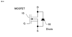
- FIG. 3B is an example showing the configuration of a semiconductor element applied to the switching elements Q13 to Q24 constituting the single-phase inverter 40, and is connected in antiparallel to the MOSFET 15 having a drain terminal D, a gate terminal G, and a source terminal S. It is composed of a diode 16.
- the MOSFET 15 may be a Si- MOSFET or, for example, a SiC- MOSFET using a wide bandgap semiconductor.
- the diode 16 may be a Si-diode or, for example, a SiC-diode using a wide bandgap semiconductor. However, it is preferable that the semiconductor device uses a wide bandgap semiconductor.
- FIG. 3C is an example showing another configuration of the semiconductor element applied to the switching elements Q13 to Q24 constituting the single-phase inverter 40, and is an example of HEMT17 having a drain terminal D, a gate terminal G, and a source terminal S and antiparallel to the HEMT17. It is composed of a connected diode 18.
- HEMT17 is, for example, a GaN-HEMT using a wide bandgap semiconductor.
- the diode 18 may be a Schottky barrier diode, a Si-diode, or, for example, a SiC-diode using a wide bandgap semiconductor. However, it is preferable that the semiconductor device uses a wide bandgap semiconductor.
- the three-phase three-level inverter 30 includes a P-side capacitor 31 and an N-side capacitor 32 connected in series, switching elements Q1 to Q4 connected in series, switching elements Q5 to switching elements Q8 connected in series, and so on.
- the switching element Q9 to the switching element Q12 connected in series are connected in parallel to the DC link capacitor 2.
- connection point E between the P-side capacitor 31 and the N-side capacitor 32 is the connection point Eu between the anode terminal of the diode D1 and the cathode terminal of the diode D2, and the connection point Ev between the anode terminal of the diode D3 and the cathode terminal of the diode D4. And the connection point Ew between the anode terminal of the diode D5 and the cathode terminal of the diode D6.
- the cathode terminal of the diode D1 is connected to the connection point Ku between the switching element Q1 and the switching element Q2
- the cathode terminal of the diode D3 is connected to the connection point Kv between the switching element Q5 and the switching element Q6, and the cathode terminal of the diode D5 is It is connected to the connection point Kw between the switching element Q9 and the switching element Q10.
- the anode terminal of the diode D2 is connected to the connection point Au between the switching element Q3 and the switching element Q4, the anode terminal of the diode D4 is connected to the connection point Av between the switching element Q7 and the switching element Q8, and the anode terminal of the diode D6 is. It is connected to the connection point Aw between the switching element Q11 and the switching element Q12.
- connection point u between the switching element Q2 and the switching element Q3, the connection point v between the switching element Q6 and the switching element Q7, and the connection point w between the switching element Q10 and the switching element Q11 are connected to the single-phase inverter 40, respectively. ..
- the switching element Q1 to the switching element Q4 connected in series have a U-phase leg
- the switching element Q5 to the switching element Q8 connected in series have a V-phase leg
- the switching element Q9 to the switching element Q12 connected in series Each constitutes a W-phase leg.
- the single-phase inverter 40 is composed of a bridge circuit of four switching elements corresponding to each phase. That is, the switching element Q13 and the switching element Q14 connected in series, the switching element Q15 and the switching element Q16 connected in series, the U-phase inverter in which the capacitor 41 is connected in parallel, and the switching element Q17 connected in series. Switching element Q18, switching element Q19 and switching element Q20 connected in series, V-phase inverter in which capacitor 41 is connected in parallel, switching element Q21 and switching element Q22 connected in series, switching element connected in series. It includes a W-phase inverter in which Q23, a switching element Q24, and a capacitor 41 are connected in parallel.
- connection point U between the switching element Q13 and the switching element Q14 is connected to the connection point u of the three-phase three-level inverter 30, and the connection point V between the switching element Q17 and the switching element Q18 is the connection point v of the three-phase three-level inverter 30.
- connection point W between the switching element Q21 and the switching element Q22 is connected to the connection point w of the three-phase three-level inverter 30.
- connection point Uo between the switching element Q15 and the switching element Q16, the connection point Vo between the switching element Q19 and the switching element Q20, and the connection point Wo between the switching element Q23 and the switching element Q24 are each connected to the load 4.
- the control device 20 receives a sensor signal from a current sensor (not shown) or a voltage sensor (not shown) provided in the three-phase three-level inverter 30 and the single-phase inverter 40, and the three-phase three-level inverter 30.
- the gate drive signal is output to the switching elements Q1 to Q24 included in the single-phase inverter 40, and control is performed so as to convert the power into a predetermined power.
- FIG. 4A is a diagram showing an output voltage command value from the target inverter 10, and here, an example of the U phase is shown.
- the output waveform is a sine wave as shown in the figure.
- FIG. 4B is a diagram showing an output voltage command value (U phase) of the three-phase three-level inverter 30, and the output waveform is a 1-pulse square wave.
- FIG. 4C shows the output voltage command value (U phase) of the single-phase inverter 40, which is the waveform of the difference between the target output waveform of FIG. 4A and the output voltage command value of the three-phase three-level inverter 30 of FIG. 4B.
- the three-phase three-level inverter 30 and the single-phase inverter 40 output a voltage according to the output voltage command value of each predetermined waveform by the gate drive signal from the control device 20.
- the three-phase three-level inverter 30 generates a one-pulse waveform by a low-frequency switching operation, and the single-phase inverter 40 has an output voltage command value generated by PWM (Pulse width modulation).
- PWM Pulse width modulation
- the voltage of each capacitor 41 of the single-phase inverter 40 is set to be smaller than the voltage of the P-side capacitor 31 and the N-side capacitor 32, which are the input capacitors of the three-phase three-level inverter 30. For example, if it is set to about 1/2 or 1/3, a stable waveform with few harmonic components can be output in the PWM operation of the single-phase inverter 40.
- the control device 20 calculates a gate drive signal using a sensor signal from a current sensor or a voltage sensor provided in the three-phase three-level inverter 30 and the single-phase inverter 40 so as to maintain the relationship of the voltage ratio of the capacitor. Output to each switching element Q1 to Q24. As a result, the three-phase three-level inverter 30 generates a one-pulse waveform by a low-frequency switching operation at a high DC voltage, and the single-phase inverter 40 performs a high-speed switching operation at a low DC voltage.
- FIG. 5A is a diagram showing a gate drive signal output to a switching element in order to output a voltage waveform corresponding to an output voltage command value (U phase) of the three-phase three-level inverter 30.
- the output voltage command value (U phase) of the three-phase three-level inverter 30 and the gate for driving the switching element Q1 to the switching element Q4 constituting the U-phase leg of the three-phase three-level inverter 30 It is a waveform of a drive signal.
- the switching element Q1 to the switching element Q4 are switched on and off once per cycle.
- the switching element constituting the three-phase three-level inverter 30 has a small number of switching times, a semiconductor element such as a Si-IGBT having a long switching time (turn-on time and turn-off time) can be used.
- the applied voltage between the collector and the emitter of the semiconductor element becomes the voltage value of the P-side capacitor 31 or the N-side capacitor 32, which is an input capacitor, during the period when the gate drive signal is off (that is, 0), and the gate drive signal is turned on (that is, that is).
- the voltage value during the period of 1) becomes 0 (actually, the voltage drop due to the inside is applied).
- FIG. 5B is a diagram showing a gate drive signal output to a switching element for outputting a voltage waveform corresponding to an output voltage command value (U phase) of the single-phase inverter 40.
- the output voltage command value and carrier wave (U phase) of the single-phase inverter 40, and the gate drive for driving the switching element Q13 to the switching element Q16 constituting the U-phase inverter of the single-phase inverter 40 It is a waveform of a signal.
- the switching element Q13 to the switching element Q16 are switched on and off a plurality of times per cycle.
- the switching element constituting the single-phase inverter 40 that operates by PWM has a large number of switchings
- a semiconductor element suitable for high-frequency driving such as SiC- MOSFET with a small switching loss may be used.
- the applied voltage between the collector and the emitter of the semiconductor element becomes the voltage value of the capacitor 41 during the period when the gate drive signal is off (that is, 0), and the voltage value during the period when the gate drive signal is on (that is, 1) becomes 0. (Actually, the voltage drop due to the inside is applied).
- each capacitor 41 of the single-phase inverter 40 smaller than the voltage of the P-side capacitor 31 and the N-side capacitor 32, which are the input capacitors of the three-phase three-level inverter 30, to 1/2 or 1/3.
- the voltage applied to the switching element constituting the single-phase inverter 40 is 1/2 or 1/3 of the voltage applied to the switching element constituting the three-phase three-level inverter 30. That is, the applied voltage differs depending on which inverter is used. Even if these are not three-phase power converters, the applied voltage can be made different in a plurality of semiconductor elements by changing the step width of the output phase voltage of each inverter.
- the SEB (Single Event Burnout) phenomenon in which a semiconductor element is destroyed by a neutron beam coming from space, is, for example, in a Si-IGBT in which a voltage is applied between a collector and an emitter, the neutron beam constitutes a Si-IGBT. It occurs when the insulation resistance of the Si-IGBT is lowered due to collision with the above. This is because if the dielectric strength of the Si-IGBT is lowered, the original withstand voltage cannot be guaranteed, or an overcurrent is energized and the element is destroyed.
- Non-Patent Document 1 the failure probability of a semiconductor element due to the SEB phenomenon tends to decrease when the voltage applied to the semiconductor element is lowered. Further, it is obvious that in the same type of semiconductor element, a semiconductor element having a high withstand voltage has a lower failure probability than a semiconductor element having a low withstand voltage. The inventors arranged these relationships using FIGS. 6A and 6B.
- FIG. 6A is a schematic diagram showing the relationship between the voltage applied to the semiconductor element and the failure probability due to the SEB phenomenon for the same type of semiconductor element having different element withstand voltage.
- the withstand voltage of the same type of element is different from low, medium, and high, for example, when the applied voltage of the semiconductor element is VA , the lower the withstand voltage of the semiconductor, the higher the failure probability.
- the failure probability decreases exponentially when the applied voltage is lowered. That is, when the operating voltage (applied voltage) is the same in semiconductor elements of the same type having different semiconductor element withstand voltage or breakdown voltage, the failure probability of the semiconductor element is inversely proportional to the element withstand voltage or breakdown voltage.
- the failure probability of an element with a high semiconductor element withstand voltage is set as a set value, and when the applied voltage of an element with a high semiconductor element withstand voltage is VA , the failure probability when an element with a medium semiconductor element withstand voltage is driven by the same applied voltage VA .
- the failure probability can be adjusted to the set value by stepping down the applied voltage of the element whose semiconductor element withstand voltage is medium to VB. That is, the failure probabilities of both can be made equal.
- the failure probability can be adjusted to the set value by stepping down the applied voltage of the device having a low withstand voltage of the semiconductor device from VA to VC .
- FIG. 6B is a schematic showing the relationship between the voltage applied to the semiconductor element and the failure probability due to SEB for the semiconductor elements of different types and having the same withstand voltage (the element withstand voltage is the same but the breakdown voltage does not have to be the same). It is a figure.
- the different types are, for example, the relationship between the IGBT and the MOSFET.
- the applied voltage of the semiconductor element is VD
- the semiconductor failure probability due to the SEB phenomenon is larger in the element B than in the element A.
- the failure probability of the element A is set as a set value
- the failure probability can be adjusted to the set value by stepping down the applied voltage of the element B from V D to VE.
- the applied voltage of the element B is V y
- the same failure probability can be adjusted by setting the applied voltage of the element A to V x .
- the element withstand voltage of the semiconductor element represents, for example, the upper limit of the voltage allowed between the collector and the emitter (in the case of MOSFET, between the drain and the source) in the IGBT, and this value is determined by each manufacturer.
- the breakdown voltage region is reached, the element causes abnormal heat generation, and the element is destroyed.
- the voltage at this time is called the breakdown voltage.
- the breakdown voltage is determined for each element (even for the same element, it may differ due to product variation).
- the voltage applied to the switching element constituting the single-phase inverter 40 is, for example, 1/2 of the voltage applied to the switching element constituting the three-phase three-level inverter 30 based on the set ratio. Or it becomes 1/3.
- the switching element constituting the three-phase three-level inverter 30 a semiconductor element having a high element withstand voltage is used because the applied voltage is high as illustrated, and the switching element constituting the single-phase inverter 40 is a semiconductor element having a medium or low applied voltage. Is used.
- the element withstand voltage and the applied voltage are set so that the failure probabilities are equal to or close to the applied voltages of both.
- the switching element constituting the three-phase three-level inverter 30 and the switching element constituting the single-phase inverter 40 are composed of different types of semiconductor elements as illustrated, according to FIG. 6B.
- the type of element and the applied voltage are set so that the failure probabilities are equal to or close to the applied voltages of both.
- the first embodiment is a power conversion device used in an environment susceptible to neutron rays such as aircraft applications, and is a power conversion device configured by using a plurality of semiconductor elements.
- the voltage applied to the semiconductor element, the withstand voltage of the semiconductor element (element withstand voltage or breakdown voltage), and the type of the element are adjusted so that the failure probabilities of a plurality of semiconductor elements are made equal to each other. It is possible to suppress the increase in size, weight and cost of the device while ensuring the above.
- a voltage is applied to each of the plurality of semiconductor elements used in the power conversion device according to the first embodiment based on a drive signal generated by the control device, but the same voltage is applied to the plurality of semiconductor elements.
- it is configured to include those with different failure probabilities due to neutron rays, and is adjusted so that the failure probabilities are the same when a voltage generated based on the drive signal is applied to each semiconductor element. be.
- the power conversion device of the first embodiment includes an inverter 10 including a three-phase three-level inverter 30 and a single-phase inverter 40, and a control device 20 for driving and controlling the inverter 10, and is a three-phase three-level inverter.
- a high withstand voltage semiconductor element is used for the switching element constituting 30, and a semiconductor element formed of a wide band gap semiconductor is used for the switching element constituting the single-phase inverter 40, and the semiconductor element fails. Since the probabilities are adjusted to be the same, in addition to the above effects, the loss associated with driving the switching element can be reduced, and a highly efficient power conversion device can be provided.
- the term “equivalent” is not limited to the case of perfect matching, but also includes the case of being slightly different within the range in which the same effect is obtained.
- FIG. 7 is a schematic configuration diagram showing the configuration of the power conversion system according to the second embodiment.
- a DC / DC converter 50 for adjusting the power supply voltage is provided between the power supply 1 and the DC link capacitor 2.
- the input voltage to the connected DC / AC inverter 10 that is, the voltage applied to the switching element is based on the voltage of the power supply 1.
- the probability of failure due to the SEB phenomenon near 0 m above sea level before takeoff increases with altitude.
- the voltage applied to the switching element is made variable so that the applied voltage can be controlled and the failure probability of the semiconductor element can be adjusted.
- FIG. 8 is a diagram showing an example of a circuit configuration of a non-insulated step-down chopper circuit as an example of the DC / DC converter 50 according to the second embodiment.
- the non-insulated step-down chopper circuit includes a switching element Q201 and a switching element Q202 connected in series, and a DC reactor 51 having one end connected to a connection point a between the switching element Q201 and the switching element Q202.
- the switching elements Q201 and Q202 are composed of a SiC-HPLC15 and a diode connected in antiparallel to the SiC-HPLC device as shown in FIG. 3B.
- FIGS. 9A and 9B are diagrams showing the applied voltage (drive signal) of the switching element of the DC / DC converter 50, which is a non-insulated step-down chopper circuit, and the voltage of the DC link capacitor 2.
- the voltage of the DC link capacitor 2 is stepped down to half of the input voltage.
- the conductivity of the switching element Q201 is 100% and the conductivity of the switching element Q202 is 0% as shown in FIG. 9B
- the voltage of the DC link capacitor 2 becomes equal to the input voltage, that is, the voltage of the power supply 1.
- the withstand voltage or breakdown voltage of the semiconductor elements constituting these switching elements is the semiconductor element constituting the switching element of the inverter 10. It is necessary to use something higher than.
- the withstand voltage of a large number (24) of the semiconductor elements constituting the switching element of the inverter 10 can be lowered, which leads to the weight reduction of the entire device.
- the applied voltage of the semiconductor element constituting the inverter 10 can be changed, and as the altitude rises.
- the applied voltage it is possible to adjust so as to reduce the failure probability and to make the failure probabilities of a plurality of semiconductor elements equal.
- the failure probability is set based on the average altitude of the aircraft equipped with the power converter during the longest cruising time.
- the applied voltage is set so that the flight cycle life determined by the failure probability at the applied voltage and the flight time set for each aircraft satisfies the preset life.
- the DC / DC converter 50 that adjusts to lower the voltage of the DC link capacitor 2 is further provided, if the same applied voltage remains, a failure occurs due to an increase in altitude. Where the probability increases, the failure probability can be reduced by reducing the applied voltage.
- the applied voltage as in the first embodiment based on the dropped voltage of the DC link capacitor 2, it is possible to adjust the failure probabilities of a plurality of semiconductor elements constituting the power conversion device to be equal. Therefore, the reliability of the power supply can be ensured.
- the semiconductor element constituting the switching element has diodes connected in antiparallel to each transistor of the IGBT, MOSFET, and HEMT.
- the semiconductor element Taking an example in which a SiC-diode is connected in anti-parallel to a SiC- MOSFET in FIG. 3B, these two semiconductor elements also have the same withstand voltage, but the failure probabilities due to SEB are different. Since the same voltage is applied to one switching element, the semiconductor element having a high failure probability is the rate-determining factor for the failure.
- the withstand voltage or breakdown voltage of the semiconductor element having a high failure probability is configured to be larger than the withstand voltage or breakdown voltage of the semiconductor element having a low failure probability.
- Embodiment 4 the power conversion device according to the fourth embodiment will be described.
- Si-IGBT is preferable for the switching element of the three-phase three-level inverter 30
- SiC- MOSFET or GaN is preferable for the switching element of the single-phase inverter 40.
- HEMTs are preferred, it is possible to make any choice different from these combinations.
- the concept when different types of semiconductor elements are used will be described below.
- Non-Patent Document 1 the failure probabilities of the SiC- MOSFET and the Si-IGBT, both of which have a withstand voltage of 1.7 kV, are shown.
- an applied voltage (bias) of 1000 V the failure probability of the Si-IGBT is larger than the failure probability of the SiC- MOSFET.
- the relationship is reversed at about 870V, and the failure probability of the Si-IGBT becomes smaller than the failure probability of the SiC-PWM.
- the element with the higher failure probability is the rate-determining element. Therefore, the withstand voltage or breakdown voltage of the semiconductor element having a high failure probability is configured to be larger than the withstand voltage or breakdown voltage of the semiconductor element having a low failure probability. As a result, considering FIGS. 6A and 6B, it is possible to make the failure probabilities equal to or closer to the same applied voltage, and to ensure the reliability of the power conversion device. Based on this idea, the type of semiconductor element can be changed in a switching element to which the same voltage is applied.
- FIG. 10 shows the above-mentioned Fig. The failure probabilities of the 1.7 kV withstand voltage SiC- MOSFET and Si-IGBT of 6b) are schematically shown.
- the solid line is a curve of the failure probability of the SiC- MOSFET and the Si-IGBT having a withstand voltage of 1.7 kV.
- This withstand voltage element it is not possible to apply an applied voltage to the SiC- MOSFET by 1/2 to 1/3 lower than that of the Si-IGBT at any applied voltage.
- the withstand voltage of the Si-IGBT is set to be larger, and the failure probability curve (Si- IGBT_ > 1.7 kV) is shown by the dotted line. As shown in the figure, 1.7 kV with respect to the applied voltage VF of the Si-IGBT. A voltage of VF / 2 is applied to the withstand voltage SiC- MOSFET, and the failure probabilities are the same.
- SiC- MOSFET having a reduced withstand voltage.
- the alternate long and short dash line in the figure is a failure probability curve (SiC- HPLC_ ⁇ 1.7 kV) with a withstand voltage of SiC-HPLC smaller than 1.7 kV, but a voltage of VF / 3 is applied and the failure probabilities are the same.
- SiC- HPLC_ ⁇ 1.7 kV failure probability curve
- the withstand voltage or breakdown voltage of the semiconductor element having a high failure probability is assumed to be larger than the withstand voltage or breakdown voltage of the semiconductor element having a low failure probability. Since it is configured so that the failure probabilities are equal to or close to each other, the reliability of the power conversion device can be ensured.
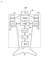
- FIG. 11 is a diagram showing an example of the aircraft 100 according to the fifth embodiment, and is a block diagram showing a state in which the power conversion device described in the first to fourth embodiments is mounted.
- the aircraft 100 is an electric power aircraft, and its propulsion system power system 60 includes a power source 63, a power source (DC power source) 1 connected to the power source 63, and a step-down chopper circuit connected to the power source 1 and converted into a predetermined voltage.
- the load 61 is a propulsion system load for obtaining a propulsive force, and is, for example, an electric motor.
- the power conversion devices of the first to fourth embodiments are used as the inverter 10 and the DC / DC converter 50 for the electric aircraft of the propulsion system power system 60 mounted on the aircraft 100. Since neutron rays increase in proportion to altitude, when a conventional power conversion device is mounted on an aircraft that flies over the sky, the failure probability increases compared to when it is used on the ground. By mounting on the propulsion system power system 60 provided with the power conversion device described in the first to fourth embodiments in consideration of the failure due to the neutron beam, the inverter 10 for the electric aircraft and the DC / DC converter for the electric aircraft can be installed.
- the failure probability of the semiconductor element used for each of the 50 can be reduced and the failure probability of the semiconductor element is made equal, it is possible to suppress the increase in size, weight and cost of the device while ensuring reliability. can do. Therefore, the fuel efficiency of the electric aircraft is also improved.
- FIG. 12 is a diagram showing an example of the aircraft 100 according to the sixth embodiment, and is a block diagram showing a state in which the power conversion device described in the first to fourth embodiments is mounted.
- the aircraft 100 is an electric aircraft, and as its equipment power system 70, a power source connected to a power source 74, an AC / DC converter 72 connected to the power source 74 to convert AC power into DC power, and an AC / DC converter 72.
- DC power supply 1, DC / DC converter 50 provided with a step-down chopper circuit connected to power supply 1 and converted to a predetermined voltage, an inverter 10 that converts DC power stepped down by the DC / DC converter 50 into AC power, and an inverter.
- a load 71 to which power is supplied from 10 and a control device 73 for controlling a DC / DC converter 50, an inverter 10, and an AC / DC converter 72 are provided.
- the load 71 is an equipment-based load, and refers to, for example, an air conditioner, an engine starter, an electric motor used for driving an auxiliary power unit, and the like.
- the power conversion devices of the first to fourth embodiments are used as the inverter 10 and the DC / DC converter 50 for the electric aircraft of the equipment-based power system 70 mounted on the aircraft 100. Since neutron rays increase in proportion to altitude, when a conventional power conversion device is mounted on an aircraft that flies over the sky, the failure probability increases compared to when it is used on the ground. By mounting it on the equipment-based power system 70 provided with the power conversion device described in the first to fourth embodiments in consideration of the failure due to the neutron beam, the same effect as that of the fifth embodiment can be obtained.
- the failure probability of the AC / DC converter 72 can be determined by designing the element so as to match the failure probabilities equally as described in the first to fourth embodiments. In addition to being able to reduce the size, it is possible to suppress the increase in size, weight, and cost of the device while ensuring reliability.
- control devices 20, 62, and 73 are composed of a processor 1000 and a storage device 2000, as shown in FIG. 13 as an example of hardware.
- the storage device includes a volatile storage device such as a random access memory and a non-volatile auxiliary storage device such as a flash memory.
- the auxiliary storage device of the hard disk may be provided instead of the flash memory.
- the processor 1000 executes the program input from the storage device 2000. In this case, the program is input from the auxiliary storage device to the processor 1000 via the volatile storage device. Further, the processor 1000 may output data such as a calculation result to the volatile storage device of the storage device 2000, or may store the data in the auxiliary storage device via the volatile storage device.
Landscapes
- Engineering & Computer Science (AREA)
- Power Engineering (AREA)
- Transportation (AREA)
- Mechanical Engineering (AREA)
- Life Sciences & Earth Sciences (AREA)
- Sustainable Development (AREA)
- Sustainable Energy (AREA)
- Aviation & Aerospace Engineering (AREA)
- Inverter Devices (AREA)
Abstract
電源(1)と負荷(4)との間に配置され、電源(1)からの電力を変換して負荷(4)に供給する電力変換装置(3)であって、半導体素子から構成される複数のスイッチング素子(Q1~Q24)と、複数のスイッチング素子(Q1~Q24)を制御する駆動信号を生成する制御装置(20)と、を備え、複数の半導体素子は制御装置(20)により生成された駆動信号に基づいてそれぞれ電圧が印加されるとともに、複数の半導体素子は中性子線による故障確率が同等となるようにして、電力変換装置(3)の中性子線による故障を防ぎ、大型化を抑制する。
Description
本願は、電力変換装置及び電力変換装置を搭載した航空機に関する。
近年、電気自動車及び船舶等において、エンジンから電動モータ駆動といった電動化システムの普及が進み、航空機に関してもCO2削減の動きから電動化への研究が世界各国で進められている。電動モータを駆動するために、電動モータに所定の電力を供給する電力変換装置が用いられる。電動航空機に搭載される電力変換装置はパワーモジュールあるいは半導体素子を具備しており、高高度環境下で使用されるため、宇宙線(中性子線)によるパワーモジュールあるいは半導体素子の偶発故障を招くことが知られており、この故障発生を防ぐための対策が求められる。また、航空機に搭載するために、実装及び燃費の観点から小型かつ軽量な電力変換装置が求められる。
このような状況において、電力変換装置を、マルチレベルインバータで構成し、高度に応じてインバータに供給する印加電圧を調整し、中性子線による偶発故障を防ぐことが開示されている(例えば、特許文献1参照)。
また、マルチレベルインバータとしては、三相インバータと単相インバータとを直列接続されたものが知られている(例えば、特許文献2参照)。
また、マルチレベルインバータとしては、三相インバータと単相インバータとを直列接続されたものが知られている(例えば、特許文献2参照)。
また、中性子線による半導体素子の故障確率は半導体素子の種類及び印加電圧に相関があることが知られている(例えば、非特許文献1参照)。
Akin Akturk, James McGarrity, Neil Goldsman, Daniel J. Lichtenwalner, Brett Hull, Dave Grider, and Richard Wilkins, "The Effects of Radiation on the Terrestrial Operation of SiC MOSFETs", 2018 IEEE international Reliability Physics Symposium, pp.2B.1-1 -2B.1-5
特許文献1に開示される技術では、航空機が閾値を超える高度に到達した場合、印加電圧を下げることで、故障を抑制することが可能である。しかし、特許文献2に示されるように、マルチレベルインバータのような電力変換装置は、多くの半導体素子を具備している。そして、非特許文献1に開示されているように、半導体素子の種類によっても宇宙からの中性子線による故障確率が異なるため、全ての半導体素子が故障しないように印加電圧を制御することは容易ではない。あるいは、過剰な耐圧を見込んで半導体素子を準備することにより電力変換装置の大型化、重量増加の虞がある。
本願は、上記の課題を解決するための技術を開示するものであり、中性子線による故障を防ぎ、かつ装置の大型化を抑制し、軽量化の可能な電力変換装置を提供することを目的とする。
本願に開示される電力変換装置は、電源と負荷との間に配置され、前記電源からの電力を変換して前記負荷に供給する電力変換装置であって、駆動信号によって制御される半導体素子をそれぞれ備えた複数のスイッチング素子と、前記駆動信号を生成する制御装置と、を備え、複数の前記半導体素子は前記制御装置により生成された前記駆動信号に基づいてそれぞれ電圧が印加されるとともに、複数の前記半導体素子は同じ前記電圧が印加された場合に中性子線による故障確率が異なるものを含み、複数の前記半導体素子は前記駆動信号に基づいて印加されるそれぞれの前記電圧に対して中性子線による故障確率が同等となるようにしたものである。
本願に開示される電力変換装置によれば、中性子線による故障を防ぎ、かつ装置の大型化を抑制し、軽量化が可能となる。また、この電力変換装置を搭載した航空機は、信頼性とともに燃費を向上させることができる。
以下、本実施の形態について図を参照して説明する。なお、各図中、同一符号は、同一または相当部分を示すものとする。
実施の形態1.
以下、実施の形態1に係る電力変換装置について図を用いて説明する。
図1は、実施の形態1に係る電力変換装置3を用いた電力変換システムの一例を示す概略構成図である。図において、電源1と負荷4との間に、DCリンクコンデンサ2及び電力変換装置3が並列に接続されている。電力変換装置3は直流電源である電源1からの電力を所定の電力に変換して負荷4に出力する電力変換部であるインバータ10とその制御部である制御装置20とを具備する。なお、本実施の形態1においてはインバータ10として、DC/ACインバータを例に説明する。
以下、実施の形態1に係る電力変換装置について図を用いて説明する。
図1は、実施の形態1に係る電力変換装置3を用いた電力変換システムの一例を示す概略構成図である。図において、電源1と負荷4との間に、DCリンクコンデンサ2及び電力変換装置3が並列に接続されている。電力変換装置3は直流電源である電源1からの電力を所定の電力に変換して負荷4に出力する電力変換部であるインバータ10とその制御部である制御装置20とを具備する。なお、本実施の形態1においてはインバータ10として、DC/ACインバータを例に説明する。
図2A、図2Bは、インバータ10の回路構成の一例を示す図で、DC/ACインバータ10は、三相3レベルインバータ30及び単相インバータ40を備えている。
図2Aにおいて、三相3レベルインバータ30を構成するスイッチング素子Q1~Q12は半導体素子であるIGBT(Integrated Gate Bipolar Transistor)にダイオードが逆並列接続された構造を有し、単相インバータ40を構成するスイッチング素子Q13~Q24は半導体素子であるMOSFET(Metal-Oxide-Semiconductor Field-Effect Transistor)にダイオードが逆並列接続された構造を有する例である。図2Bにおいて、三相3レベルインバータ30を構成するスイッチング素子Q1~Q12は図2Aと同様に半導体素子であるIGBTにダイオードが逆並列接続された構造を有し、単相インバータ40を構成するスイッチング素子Q13~Q24は半導体素子であるHEMT(High Electron Mobility Transistor)にダイオードが逆並列接続された構造を有する例である。
図2Aにおいて、三相3レベルインバータ30を構成するスイッチング素子Q1~Q12は半導体素子であるIGBT(Integrated Gate Bipolar Transistor)にダイオードが逆並列接続された構造を有し、単相インバータ40を構成するスイッチング素子Q13~Q24は半導体素子であるMOSFET(Metal-Oxide-Semiconductor Field-Effect Transistor)にダイオードが逆並列接続された構造を有する例である。図2Bにおいて、三相3レベルインバータ30を構成するスイッチング素子Q1~Q12は図2Aと同様に半導体素子であるIGBTにダイオードが逆並列接続された構造を有し、単相インバータ40を構成するスイッチング素子Q13~Q24は半導体素子であるHEMT(High Electron Mobility Transistor)にダイオードが逆並列接続された構造を有する例である。
ここで、三相3レベルインバータ30を構成するスイッチング素子Q1~Q12及び単相インバータ40を構成するスイッチング素子Q13~Q24はいずれもワイドバンドギャップ半導体を用いて形成されたものが好ましい。詳細は後述するが、特に単相インバータ40を構成するスイッチング素子Q13~Q24は高速スイッチングを行うので、ワイドバンドギャップ半導体を用いて形成されたスイッチング素子がより好適である。
図2A、図2Bの三相3レベルインバータ30及び単相インバータ40を構成するスイッチング素子Q1~Q24の構造を図3A、図3B、図3Cを用いて説明する。
図3Aは、三相3レベルインバータ30を構成するスイッチング素子Q1からQ12に適用される半導体素子の構成を示す一例で、コレクタ端子C、ゲート端子G、エミッタ端子Eを有するIGBT13とこれに逆並列接続されたダイオード14とで構成される。IGBT13は、Si-IGBTであっても、ワイドバンドギャップ半導体を用いた例えばSiC-IGBTであってもよい。また、ダイオード14はSi-ダイオードであっても、ワイドバンドギャップ半導体を用いた例えばSiC-ダイオードであってもよい。
図3Aは、三相3レベルインバータ30を構成するスイッチング素子Q1からQ12に適用される半導体素子の構成を示す一例で、コレクタ端子C、ゲート端子G、エミッタ端子Eを有するIGBT13とこれに逆並列接続されたダイオード14とで構成される。IGBT13は、Si-IGBTであっても、ワイドバンドギャップ半導体を用いた例えばSiC-IGBTであってもよい。また、ダイオード14はSi-ダイオードであっても、ワイドバンドギャップ半導体を用いた例えばSiC-ダイオードであってもよい。
図3Bは、単相インバータ40を構成するスイッチング素子Q13~Q24に適用される半導体素子の構成を示す一例で、ドレイン端子D、ゲート端子G、ソース端子Sを有するMOSFET15とこれに逆並列接続されたダイオード16とで構成される。MOSFET15は、Si-MOSFETであっても、ワイドバンドギャップ半導体を用いた例えばSiC-MOSFETであってもよい。また、ダイオード16はSi-ダイオードであっても、ワイドバンドギャップ半導体を用いた例えばSiC-ダイオードであってもよい。しかし、望ましくはワイドバンドギャップ半導体を用いた半導体素子である方がよい。
図3Cは、単相インバータ40を構成するスイッチング素子Q13~Q24に適用される半導体素子の別の構成を示す一例で、ドレイン端子D、ゲート端子G、ソース端子Sを有するHEMT17とこれに逆並列接続されたダイオード18とで構成される。HEMT17は、例えばワイドバンドギャップ半導体を用いたGaN-HEMTである。また、ダイオード18はショットキーバリアダイオード、Si-ダイオードであっても、ワイドバンドギャップ半導体を用いた例えばSiC-ダイオードであってもよい。しかし、望ましくはワイドバンドギャップ半導体を用いた半導体素子である方がよい。
次に、図2Aを用いて、インバータ10の回路構成について説明する。
図2Aにおいて、三相3レベルインバータ30は、直列接続されたP側コンデンサ31とN側コンデンサ32、直列接続されたスイッチング素子Q1~スイッチング素子Q4、直列接続されたスイッチング素子Q5~スイッチング素子Q8、直列接続されたスイッチング素子Q9~スイッチング素子Q12がDCリンクコンデンサ2に並列接続されて構成されている。
図2Aにおいて、三相3レベルインバータ30は、直列接続されたP側コンデンサ31とN側コンデンサ32、直列接続されたスイッチング素子Q1~スイッチング素子Q4、直列接続されたスイッチング素子Q5~スイッチング素子Q8、直列接続されたスイッチング素子Q9~スイッチング素子Q12がDCリンクコンデンサ2に並列接続されて構成されている。
P側コンデンサ31とN側コンデンサ32との接続点Eは、ダイオードD1のアノード端子とダイオードD2のカソード端子との接続点Eu、ダイオードD3のアノード端子とダイオードD4のカソード端子との接続点Ev、及びダイオードD5のアノード端子とダイオードD6のカソード端子との接続点Ewと接続されている。
ダイオードD1のカソード端子はスイッチング素子Q1とスイッチング素子Q2との接続点Kuと接続され、ダイオードD3のカソード端子はスイッチング素子Q5とスイッチング素子Q6との接続点Kvと接続され、ダイオードD5のカソード端子はスイッチング素子Q9とスイッチング素子Q10との接続点Kwと接続されている。
ダイオードD2のアノード端子はスイッチング素子Q3とスイッチング素子Q4との接続点Auと接続され、ダイオードD4のアノード端子はスイッチング素子Q7とスイッチング素子Q8との接続点Avと接続され、ダイオードD6のアノード端子はスイッチング素子Q11とスイッチング素子Q12との接続点Awと接続されている。
スイッチング素子Q2とスイッチング素子Q3との接続点u、スイッチング素子Q6とスイッチング素子Q7との接続点v、及びスイッチング素子Q10とスイッチング素子Q11との接続点wはそれぞれ単相インバータ40に接続されている。
直列に接続されたスイッチング素子Q1~スイッチング素子Q4はU相のレグを、直列に接続されたスイッチング素子Q5~スイッチング素子Q8はV相のレグを、直列に接続されたスイッチング素子Q9~スイッチング素子Q12はW相のレグをそれぞれ構成する。
直列に接続されたスイッチング素子Q1~スイッチング素子Q4はU相のレグを、直列に接続されたスイッチング素子Q5~スイッチング素子Q8はV相のレグを、直列に接続されたスイッチング素子Q9~スイッチング素子Q12はW相のレグをそれぞれ構成する。
単相インバータ40は、各相に対応した4つのスイッチング素子のブリッジ回路で構成されている。すなわち、直列に接続されたスイッチング素子Q13とスイッチング素子Q14、直列に接続されたスイッチング素子Q15とスイッチング素子Q16、及びコンデンサ41が並列に接続されたU相インバータ、直列に接続されたスイッチング素子Q17とスイッチング素子Q18、直列に接続されたスイッチング素子Q19とスイッチング素子Q20、及びコンデンサ41が並列に接続されたV相インバータ、直列に接続されたスイッチング素子Q21とスイッチング素子Q22、直列に接続されたスイッチング素子Q23とスイッチング素子Q24、及びコンデンサ41が並列に接続されたW相インバータを備えている。
スイッチング素子Q13とスイッチング素子Q14との接続点Uは三相3レベルインバータ30の接続点uと接続され、スイッチング素子Q17とスイッチング素子Q18との接続点Vは三相3レベルインバータ30の接続点vと接続され、スイッチング素子Q21とスイッチング素子Q22との接続点Wは三相3レベルインバータ30の接続点wとそれぞれ接続されている。
スイッチング素子Q15とスイッチング素子Q16との接続点Uo、スイッチング素子Q19とスイッチング素子Q20との接続点Vo、スイッチング素子Q23とスイッチング素子Q24との接続点Woは、それぞれ負荷4に接続される。
制御装置20は、三相3レベルインバータ30及び単相インバータ40に設けられた電流センサ(図示せず)あるいは電圧センサ(図示せず)からのセンサ信号を受信するとともに、三相3レベルインバータ30及び単相インバータ40の具備するスイッチング素子Q1~Q24にゲート駆動信号を出力し、所定の電力に変換するように制御を行う。
次に、実施の形態1に係る電力変換装置3の動作について説明する。
図4Aは、目標とするインバータ10からの出力電圧指令値を示す図で、ここではU相の例を示している。出力波形は図のように正弦波である。図4Bは三相3レベルインバータ30の出力電圧指令値(U相)を示す図で、出力波形は1パルスの方形波である。図4Cに、単相インバータ40の出力電圧指令値(U相)を示すが、図4Aの目標出力波形と図4Bの三相3レベルインバータ30の出力電圧指令値の差分の波形となる。
図4Aは、目標とするインバータ10からの出力電圧指令値を示す図で、ここではU相の例を示している。出力波形は図のように正弦波である。図4Bは三相3レベルインバータ30の出力電圧指令値(U相)を示す図で、出力波形は1パルスの方形波である。図4Cに、単相インバータ40の出力電圧指令値(U相)を示すが、図4Aの目標出力波形と図4Bの三相3レベルインバータ30の出力電圧指令値の差分の波形となる。
三相3レベルインバータ30及び単相インバータ40は、制御装置20からのゲート駆動信号により、それぞれの所定の波形の出力電圧指令値により電圧を出力する。
三相3レベルインバータ30は、低周波のスイッチング動作により、ワンパルスの波形を生成し、単相インバータ40は出力電圧指令値がPWM(Pulse width Modulation:パルス幅変調)により生成された波形であるため、多数のパルス状の電圧波形を生成する。そのため、単相インバータ40の各コンデンサ41の電圧が、三相3レベルインバータ30の入力コンデンサであるP側コンデンサ31及びN側コンデンサ32の電圧より小さくなるように設定する。例えば、1/2あるいは1/3程度に設定すれば、単相インバータ40のPWM動作において高調波成分の少ない安定した波形を出力することができる。
三相3レベルインバータ30は、低周波のスイッチング動作により、ワンパルスの波形を生成し、単相インバータ40は出力電圧指令値がPWM(Pulse width Modulation:パルス幅変調)により生成された波形であるため、多数のパルス状の電圧波形を生成する。そのため、単相インバータ40の各コンデンサ41の電圧が、三相3レベルインバータ30の入力コンデンサであるP側コンデンサ31及びN側コンデンサ32の電圧より小さくなるように設定する。例えば、1/2あるいは1/3程度に設定すれば、単相インバータ40のPWM動作において高調波成分の少ない安定した波形を出力することができる。
制御装置20は、コンデンサの電圧比の関係を保つように、三相3レベルインバータ30及び単相インバータ40に設けられた電流センサあるいは電圧センサからのセンサ信号を用いてゲート駆動信号を演算し、各スイッチング素子Q1~Q24に出力する。その結果、三相3レベルインバータ30は、高い直流電圧で低周波のスイッチング動作によりワンパルスの波形を生成し、単相インバータ40は低い直流電圧で高速スイッチング動作を行うことになる。
図5Aは、三相3レベルインバータ30の出力電圧指令値(U相)に対応する電圧波形を出力するためにスイッチング素子に出力されるゲート駆動信号を示す図である。図において、上から順に、三相3レベルインバータ30の出力電圧指令値(U相)、三相3レベルインバータ30のU相のレグを構成するスイッチング素子Q1~スイッチング素子Q4を駆動するためのゲート駆動信号の波形である。スイッチング素子Q1~スイッチング素子Q4は一周期当たりオン及びオフが1回ずつスイッチングする。そのため、三相3レベルインバータ30を構成するスイッチング素子はスイッチング回数が少ないので、スイッチング時間(ターンオン時間及びターンオフ時間)が長いSi-IGBT等の半導体素子を使用することができる。このとき半導体素子のコレクタ―エミッタ間の印加電圧はゲート駆動信号がオフ(すなわち0)の期間に入力コンデンサであるP側コンデンサ31またはN側コンデンサ32の電圧値となり、ゲート駆動信号がオン(すなわち1)の期間の電圧値は0となる(実際には内部による電圧降下分印加される)。
図5Bは、単相インバータ40の出力電圧指令値(U相)に対応する電圧波形を出力するためのスイッチング素子に出力されるゲート駆動信号を示す図である。図において、上から順に、単相インバータ40の出力電圧指令値及びキャリア波(U相)、単相インバータ40のU相のインバータを構成するスイッチング素子Q13~スイッチング素子Q16を駆動するためのゲート駆動信号の波形である。スイッチング素子Q13~スイッチング素子Q16は一周期当たり複数回ずつオン及びオフスイッチングする。PWM動作する単相インバータ40を構成するスイッチング素子はスイッチング回数が多いので、スイッチング損失の小さいSiC-MOSFET等の高周波駆動に適した半導体素子を使用すればよい。このとき半導体素子のコレクタ―エミッタ間の印加電圧はゲート駆動信号がオフ(すなわち0)の期間にコンデンサ41の電圧値となり、ゲート駆動信号がオン(すなわち1)の期間の電圧値は0となる(実際には内部による電圧降下分印加される)。
単相インバータ40の各コンデンサ41の電圧が、三相3レベルインバータ30の入力コンデンサであるP側コンデンサ31及びN側コンデンサ32の電圧より小さくなるように、例えば、1/2あるいは1/3に設定した場合、単相インバータ40を構成するスイッチング素子に印加される電圧は、三相3レベルインバータ30を構成するスイッチング素子に印加される電圧の1/2あるいは1/3となる。すなわち、いずれのインバータに用いられるかによって印加電圧が異なることになる。これらは3相の電力変換装置でなくても各インバータの出力相電圧のステップ幅を変えることにより複数半導体素子において印加電圧を異ならせることができる。
次に、中性子線による半導体素子の偶発故障と半導体素子に印加される電圧との関係について説明する。
宇宙から飛来する中性子線により半導体素子が破壊されるSEB(Single Event Burnout)現象は、例えば、コレクタとエミッタ間に電圧が印加されたSi-IGBTにおいて、中性子線がSi-IGBTを構成するSi原子等に衝突し、Si-IGBTの絶縁耐量が低下することで生じる。Si-IGBTの絶縁耐量が低下すると、本来の耐圧を担保できない、あるいは過電流が通電され素子破壊に至るためである。このSEB現象による故障は確率的に発生するものであり、中性子線量に比例して故障確率は上昇するため、高度が高いほど故障確率が上昇することが知られている。また、この現象により発生する偶発故障の耐性を表した指標としてLTDS(Long Term DC Stability)があり、これを用いて半導体素子の故障確率を記述することができる。
宇宙から飛来する中性子線により半導体素子が破壊されるSEB(Single Event Burnout)現象は、例えば、コレクタとエミッタ間に電圧が印加されたSi-IGBTにおいて、中性子線がSi-IGBTを構成するSi原子等に衝突し、Si-IGBTの絶縁耐量が低下することで生じる。Si-IGBTの絶縁耐量が低下すると、本来の耐圧を担保できない、あるいは過電流が通電され素子破壊に至るためである。このSEB現象による故障は確率的に発生するものであり、中性子線量に比例して故障確率は上昇するため、高度が高いほど故障確率が上昇することが知られている。また、この現象により発生する偶発故障の耐性を表した指標としてLTDS(Long Term DC Stability)があり、これを用いて半導体素子の故障確率を記述することができる。
一方、非特許文献1によれば、SEB現象による半導体素子の故障確率は半導体素子に印加される電圧を下げると、故障確率は下がる傾向にある。また、同種の半導体素子において、耐圧が高い半導体素子は耐圧が低い半導体素子より故障確率が低いことは自明である。発明者らはこれらの関係を図6A及び図6Bを用いて整理した。
図6Aは、異なる素子耐圧を有する同種の半導体素子について、半導体素子への印加電圧とSEB現象による故障確率との関係を示す模式図である。同種素子の耐圧が低、中、高と異なる場合において、例えば半導体素子印加電圧がVAの時、半導体耐圧が低いほど故障確率が大きくなる。また、これら半導体のLTDS特性により、印加電圧を下げると故障確率は指数関数的に減少する。すなわち半導体素子耐圧またはブレークダウン電圧が異なる同種類の半導体素子において動作電圧(印加電圧)が等しい場合に半導体素子の故障確率は素子耐圧またはブレークダウン電圧に反比例する。
図において、半導体素子耐圧が高い素子の故障確率を設定値とし、半導体素子耐圧が高い素子の印加電圧がVAの時、半導体素子耐圧が中の素子を同じ印加電圧VAで駆動すると故障確率が大きくなってしまうが、半導体素子耐圧が中の素子の印加電圧をVBに降圧することで故障確率を設定値に調整できる。すなわち、両者の故障確率を同等にすることができる。同様に半導体素子耐圧が低い素子の印加電圧をVAからVCに降圧することで故障確率を設定値に調整できる。
図6Bは、種類が異なり、同耐圧(素子耐圧が等しいが、ブレークダウン電圧は等しくなくてもよい)である半導体素子について、半導体素子への印加電圧とSEBによる故障確率との関係を示す模式図である。種類が異なるとは、例えばIGBTとMOSFETとの関係である。図において、半導体素子印加電圧がVDでは、SEB現象による半導体故障確率は素子Bの方が素子Aより大きい。素子Aの故障確率を設定値とするとき、素子Bの印加電圧をVDからVEに降圧することで故障確率を設定値に調整できる。また、素子Bの印加電圧がVyにおいては、素子Aの印加電圧をVxにすることで同等の故障確率に調整できる。
ここで、半導体素子の素子耐圧は、例えばIGBTではコレクタ-エミッタ間(MOSFETであればドレイン-ソース間)に許容される電圧上限値を表しており、この値は各製造メーカによって定められる。半導体素子の素子耐圧により制限される値を超えた電圧が印加された場合、ブレークダウン電圧領域に達し、素子が異常発熱を起こし、破壊に至る。このときの電圧をブレークダウン電圧と言う。ブレークダウン電圧は素子ごとに決まっている(同一素子においても製品バラツキにより異なる場合がある)。
以上の知見から、本実施の形態のインバータ10を構成する半導体素子の故障確率の調整方法について説明する。
上述のとおり、単相インバータ40を構成するスイッチング素子に印加される電圧は、設定された比率に基づいて、三相3レベルインバータ30を構成するスイッチング素子に印加される電圧の例えば、1/2あるいは1/3となる。三相3レベルインバータ30を構成するスイッチング素子は、例示したように印加電圧が高いので素子耐圧の高い半導体素子を用い、単相インバータ40を構成するスイッチング素子には印加電圧の中または低い半導体素子を用いる。このとき、図6A及び図6Bに従って、両者の印加電圧に対して故障確率が同等あるいは近くなるように、素子耐圧及び印加電圧の設定を行う。
上述のとおり、単相インバータ40を構成するスイッチング素子に印加される電圧は、設定された比率に基づいて、三相3レベルインバータ30を構成するスイッチング素子に印加される電圧の例えば、1/2あるいは1/3となる。三相3レベルインバータ30を構成するスイッチング素子は、例示したように印加電圧が高いので素子耐圧の高い半導体素子を用い、単相インバータ40を構成するスイッチング素子には印加電圧の中または低い半導体素子を用いる。このとき、図6A及び図6Bに従って、両者の印加電圧に対して故障確率が同等あるいは近くなるように、素子耐圧及び印加電圧の設定を行う。
また、スイッチング周波数の観点で、例示したように三相3レベルインバータ30を構成するスイッチング素子と単相インバータ40を構成するスイッチング素子とを異なる種類の半導体素子で構成した場合は、図6Bに従って、両者の印加電圧に対して故障確率が同等あるいは近くなるように、素子の種類及び印加電圧の設定を行う。
複数の半導体素子を備えた電力変換装置においては、例えば、一部に故障確率の著しく低い素子を用いていてもそのメリットを活かせず、全体として信頼性確保のために過剰な耐圧品の使用等の手当をして装置の大型化、重量化及びコストの増加を招いていた。本実施の形態においては、電力変換装置を構成する半導体素子の故障確率を同等あるいは近くなるように設定するので、信頼性を確保しつつ装置の大型化、重量化及びコストの増加を抑制することができる。
なお、インバータ10の動作及びインバータ10を構成する半導体素子の故障確率の調整方法等については、図2Aの構成を中心に説明したが、図2Bの単相インバータ40を構成するスイッチング素子Q13~Q24は半導体素子であるHEMTにダイオードが逆並列接続された構造の例であっても同様であるので、説明は省略する。
以上のように、本実施の形態1によれば、航空機用途等の中性子線の影響を受けやすい環境において使用される電力変換装置であって、複数の半導体素子を用いて構成された電力変換装置3において、半導体素子に印加される電圧、半導体素子の耐圧(素子耐圧またはブレークダウン電圧)、素子の種類を調整することにより複数の半導体素子の故障確率を同等となるようにしたので、信頼性を確保しつつ装置の大型化、重量化及びコストの増加を抑制することができる。
すなわち、実施の形態1に係る電力変換装置に用いられる複数の半導体素子は、制御装置により生成された駆動信号に基づいてそれぞれ電圧が印加されるが、複数の前記半導体素子は同じ電圧が印加された場合に中性子線による故障確率が異なるものを含むように構成し、それぞれの半導体素子に駆動信号に基づいて生成された電圧が印加されたときに故障確率が同様となるように調整するものである。
また、本実施の形態1の電力変換装置は、三相3レベルインバータ30と単相インバータ40とを備えたインバータ10、及びインバータ10の駆動制御を行う制御装置20を備え、三相3レベルインバータ30を構成するスイッチング素子には高耐圧の半導体素子を用い、単相インバータ40を構成するスイッチング素子には、ワイドバンドギャップ半導体により形成された半導体素子を用いて構成し、それらの半導体素子の故障確率を同等となるように調整したので、上記の効果に加え、スイッチング素子の駆動に伴う損失も低減し、高効率な電力変換装置を提供することができる。
なお、故障確率を同等となるように調整する場合は、故障確率の低い素子に合わせるように耐圧、印加電圧等を調整することが望ましいことは言うまでもない。
また、同等とは、完全に一致する場合に限らず、同様の効果が奏される範囲で、多少異なる場合も含む。
また、同等とは、完全に一致する場合に限らず、同様の効果が奏される範囲で、多少異なる場合も含む。
実施の形態2.
以下、実施の形態2に係る電力変換装置について図を用いて説明する。
図7は、実施の形態2に係る電力変換システムの構成を示す概略構成図である。実施の形態1の図1との違いは、電源電圧を調整するためのDC/DCコンバータ50を電源1とDCリンクコンデンサ2との間に設けたことである。実施の形態1においては、接続しDC/ACインバータ10への入力電圧すなわちスイッチング素子に印加される電圧は電源1の電圧が基準となっていた。しかし、航空機の離陸前後では電力変換装置を動作させながら高度を上昇させるため、離陸前の海抜0m付近でのSEB現象による故障確率は高度に伴い増加する。DC/ACインバータ10へ入力電圧が一定では、高度上昇に伴う半導体素子の故障確率を低減することは困難である。そのため、スイッチング素子に印加する電圧を可変にし、印加電圧を制御可能として半導体素子の故障確率を調整できるようにした。
以下、実施の形態2に係る電力変換装置について図を用いて説明する。
図7は、実施の形態2に係る電力変換システムの構成を示す概略構成図である。実施の形態1の図1との違いは、電源電圧を調整するためのDC/DCコンバータ50を電源1とDCリンクコンデンサ2との間に設けたことである。実施の形態1においては、接続しDC/ACインバータ10への入力電圧すなわちスイッチング素子に印加される電圧は電源1の電圧が基準となっていた。しかし、航空機の離陸前後では電力変換装置を動作させながら高度を上昇させるため、離陸前の海抜0m付近でのSEB現象による故障確率は高度に伴い増加する。DC/ACインバータ10へ入力電圧が一定では、高度上昇に伴う半導体素子の故障確率を低減することは困難である。そのため、スイッチング素子に印加する電圧を可変にし、印加電圧を制御可能として半導体素子の故障確率を調整できるようにした。
図8は、実施の形態2に係るDC/DCコンバータ50の一例として、非絶縁降圧チョッパ回路の回路構成の一例を示す図である。図において、非絶縁降圧チョッパ回路は、直列に接続されたスイッチング素子Q201及びスイッチング素子Q202と、スイッチング素子Q201とスイッチング素子Q202との接続点aに一端が接続されたDCリアクトル51とを備える。スイッチング素子Q201、Q202は図3Bで示したような、SiC-MOSFET15これに逆並列接続されたダイオードとで構成される。
図9A、図9Bは、非絶縁降圧チョッパ回路であるDC/DCコンバータ50のスイッチング素子の印加電圧(駆動信号)及びDCリンクコンデンサ2の電圧を示す図である。図9Aのようにスイッチング素子Q201、Q202の導通率を50%とすると、DCリンクコンデンサ2の電圧は入力電圧の半分に降圧される。また、図9Bのようにスイッチング素子Q201の導通率が100%、スイッチング素子Q202の導通率が0%とすると、DCリンクコンデンサ2の電圧は入力電圧すなわち、電源1の電圧と等しくなる。
このように、スイッチング素子Q201、Q202を駆動するゲート電圧の通電率に応じてDCリンクコンデンサ2に印加される電圧を、
DCリンクコンデンサ電圧=入力電圧×スイッチング素子Q201の導通率
で調整することができる。
このように、スイッチング素子Q201、Q202を駆動するゲート電圧の通電率に応じてDCリンクコンデンサ2に印加される電圧を、
DCリンクコンデンサ電圧=入力電圧×スイッチング素子Q201の導通率
で調整することができる。
このDC/DCコンバータ50のスイッチング素子Q201、Q202には電源電圧と等しい電圧が印加されるため、これらスイッチング素子を構成する半導体素子の耐圧またはブレークダウン電圧はインバータ10のスイッチング素子を構成する半導体素子よりも高いもの用いる必要がある。インバータ10のスイッチング素子を構成する多数の(24個)の半導体素子の耐圧を低くすることができ、装置全体の軽量化につながる。
また、このように非絶縁降圧チョッパであるDC/DCコンバータ50のスイッチング素子Q201、Q202の導通率を調整することでインバータ10を構成する半導体素子の印加電圧を変えることができ、高度上昇に伴い、印加電圧を下げることで故障確率を低減するように調整するとともに、複数の半導体素子の故障確率を同等にするように調整することが可能となる。例えば、故障確率は電力変換装置が搭載される航空機の運航時間の最も長い巡航時の平均高度に基づいて設定する。また、印加電圧は、その印加電圧における故障確率と機体毎に設定された飛行時間とで決まる飛行サイクル寿命が、予め設定された寿命を満たすように、設定する。
以上のように、実施の形態2によれば、DCリンクコンデンサ2の電圧を降下させるように調整するDC/DCコンバータ50をさらに設けたので、同じ印加電圧のままであると高度上昇に伴い故障確率が増加するところを、印加電圧を低減することで、故障確率を低減することができる。降下したDCリンクコンデンサ2の電圧に基づいて、実施の形態1のように印加電圧を調整すれば、電力変換装置を構成する複数の半導体素子の故障確率を同等にするように調整することが可能となり、電力装置の信頼性を確保することができる。
実施の形態3.
以下、実施の形態3に係る電力変換装置について説明する。
スイッチング素子を構成する半導体素子は図3A~図3Cに示したように、IGBT、MOSFET、HEMTの各トランジスタにダイオードが逆並列接続されている。図3BでSiC-MOSFETにSiC-ダイオードが逆並列接続されている例をとると、この2つの半導体素子も同じ耐圧に対し、SEBによる故障確率が異なる。1つのスイッチング素子には同じ電圧が印加されることから、故障確率の高い半導体素子が故障に対して律速となる。そこで、故障確率の高い半導体素子の耐圧またはブレークダウン電圧を故障確率の低い半導体素子の耐圧またはブレークダウン電圧よりも大きいものとして構成する。これにより、図6A及び図6Bを考慮すると、同じ印加電圧に対して、故障確率を同等あるいは近づけることが可能となり、電力変換装置の信頼性を確保することができる。
以下、実施の形態3に係る電力変換装置について説明する。
スイッチング素子を構成する半導体素子は図3A~図3Cに示したように、IGBT、MOSFET、HEMTの各トランジスタにダイオードが逆並列接続されている。図3BでSiC-MOSFETにSiC-ダイオードが逆並列接続されている例をとると、この2つの半導体素子も同じ耐圧に対し、SEBによる故障確率が異なる。1つのスイッチング素子には同じ電圧が印加されることから、故障確率の高い半導体素子が故障に対して律速となる。そこで、故障確率の高い半導体素子の耐圧またはブレークダウン電圧を故障確率の低い半導体素子の耐圧またはブレークダウン電圧よりも大きいものとして構成する。これにより、図6A及び図6Bを考慮すると、同じ印加電圧に対して、故障確率を同等あるいは近づけることが可能となり、電力変換装置の信頼性を確保することができる。
実施の形態4.
以下、実施の形態4に係る電力変換装置について説明する。
実施の形態1から3では、図2A、図2Bで示したように、三相3レベルインバータ30のスイッチング素子にはSi-IGBTが好ましく、単相インバータ40のスイッチング素子にはSiC-MOSFETまたはGaN-HEMTが好ましいと述べたが、これらの組み合わせとは異なる任意の選択を行うことも可能である。種類の異なる半導体素子を用いる場合の考え方について以下に説明する。
以下、実施の形態4に係る電力変換装置について説明する。
実施の形態1から3では、図2A、図2Bで示したように、三相3レベルインバータ30のスイッチング素子にはSi-IGBTが好ましく、単相インバータ40のスイッチング素子にはSiC-MOSFETまたはGaN-HEMTが好ましいと述べたが、これらの組み合わせとは異なる任意の選択を行うことも可能である。種類の異なる半導体素子を用いる場合の考え方について以下に説明する。
非特許文献1のFig.6b)には共に1.7kV耐圧のSiC-MOSFETとSi-IGBTの故障確率が示されている。印加電圧(バイアス)1000VにおいてはSi-IGBTの故障確率はSiC-MOSFETの故障確率より大きい。しかし、印加電圧を下げていき、約870Vを境にその関係は逆転し、Si-IGBTの故障確率はSiC-MOSFETの故障確率より小さくなる。
同耐圧で種類の異なる素子においては、故障確率の高い方の素子が律速となる。そのため、故障確率の高い半導体素子の耐圧またはブレークダウン電圧を故障確率の低い半導体素子の耐圧またはブレークダウン電圧よりも大きいものとして構成する。これにより、図6A及び図6Bを考慮すると、同じ印加電圧に対して、故障確率を同等あるいは近づけることが可能となり、電力変換装置の信頼性を確保することができる。このような考え方で同じ電圧印加されるスイッチング素子において半導体素子の種類を変更することができる。
一方、実施の形態1から3において、図2Aの構成によれば、三相3レベルインバータ30のスイッチング素子にSi-IGBTを用い、単相インバータ40のスイッチング素子にSiC-MOSFETを用いた場合、単相インバータ40のスイッチング素子のSiC-MOSFETには三相3レベルインバータ30のスイッチング素子のSi-IGBTよりも1/2から1/3低い印加電圧を与えることが好ましいとされている。
図10に、上述の非特許文献1のFig.6b)の1.7kV耐圧のSiC-MOSFETとSi-IGBTの故障確率を模式的に示す。実線は1.7kV耐圧のSiC-MOSFETとSi-IGBTの故障確率の曲線である。この耐圧の素子ではいずれの印加電圧においても、SiC-MOSFETにSi-IGBTよりも1/2から1/3低い印加電圧を与えることはできない。Si-IGBTの耐圧をさらに大きなものを設定し、その故障確率曲線(Si-IGBT_>1.7kV)を点線に示すが、図のようにSi-IGBTの印加電圧VFに対し、1.7kV耐圧のSiC-MOSFETにはVF/2の電圧が印加され、かつ故障確率が同等となる。さらに、SiC-MOSFETはSi-IGBTより印加電圧が小さいことがわかっているので、耐圧を下げたSiC-MOSFETを用いることもできる。図中一点鎖線はSiC-MOSFETの耐圧を1.7kVより小さなものの故障確率曲線(SiC-MOSFET_<1.7kV)であるが、VF/3の電圧が印加され、かつ故障確率が同等となるように設定可能となる。
図10に、上述の非特許文献1のFig.6b)の1.7kV耐圧のSiC-MOSFETとSi-IGBTの故障確率を模式的に示す。実線は1.7kV耐圧のSiC-MOSFETとSi-IGBTの故障確率の曲線である。この耐圧の素子ではいずれの印加電圧においても、SiC-MOSFETにSi-IGBTよりも1/2から1/3低い印加電圧を与えることはできない。Si-IGBTの耐圧をさらに大きなものを設定し、その故障確率曲線(Si-IGBT_>1.7kV)を点線に示すが、図のようにSi-IGBTの印加電圧VFに対し、1.7kV耐圧のSiC-MOSFETにはVF/2の電圧が印加され、かつ故障確率が同等となる。さらに、SiC-MOSFETはSi-IGBTより印加電圧が小さいことがわかっているので、耐圧を下げたSiC-MOSFETを用いることもできる。図中一点鎖線はSiC-MOSFETの耐圧を1.7kVより小さなものの故障確率曲線(SiC-MOSFET_<1.7kV)であるが、VF/3の電圧が印加され、かつ故障確率が同等となるように設定可能となる。
以上のように、実施の形態4によれば、種類の異なる半導体素子については故障確率の高い半導体素子の耐圧またはブレークダウン電圧を故障確率の低い半導体素子の耐圧またはブレークダウン電圧よりも大きいものとして構成して、故障確率を同等あるいは近づけるようにしたので、電力変換装置の信頼性を確保することができる。
実施の形態5.
以下、実施の形態5に係る航空機について説明する。
図11は、実施の形態5に係る航空機100の一例を示す図で、実施の形態1から4で説明した電力変換装置が搭載された状態を示すブロック図である。航空機100は電動航空機であり、その推進系電力システム60として、電力源63、電力源63に接続された電源(DC電源)1、電源1に接続され所定の電圧に変換する降圧チョッパ回路を備えたDC/DCコンバータ50、DC/DCコンバータ50で降圧された直流電力を交流電力に変換するインバータ10、インバータ10から電力が供給される負荷61、及びDC/DCコンバータ50、インバータ10を制御する制御装置62を備える。ここで負荷61は推進力を得るための推進系負荷であり、例えば電動モータである。
以下、実施の形態5に係る航空機について説明する。
図11は、実施の形態5に係る航空機100の一例を示す図で、実施の形態1から4で説明した電力変換装置が搭載された状態を示すブロック図である。航空機100は電動航空機であり、その推進系電力システム60として、電力源63、電力源63に接続された電源(DC電源)1、電源1に接続され所定の電圧に変換する降圧チョッパ回路を備えたDC/DCコンバータ50、DC/DCコンバータ50で降圧された直流電力を交流電力に変換するインバータ10、インバータ10から電力が供給される負荷61、及びDC/DCコンバータ50、インバータ10を制御する制御装置62を備える。ここで負荷61は推進力を得るための推進系負荷であり、例えば電動モータである。
実施の形態1から4の電力変換装置は、航空機100に搭載される推進系電力システム60の電動航空機用のインバータ10、DC/DCコンバータ50として用いられる。中性子線は高度に比例して増加するため、航空機のように上空を飛行するものに従来の電力変換装置を搭載した場合、故障確率が地上で使用する場合に比べて増加する。中性子線による故障を考慮した実施の形態1から4で説明した電力変換装置を備えた推進系電力システム60に搭載することで、電動航空機用としてのインバータ10、電動航空機用としてのDC/DCコンバータ50それぞれに用いられる半導体素子の故障確率を下げることができるとともに、半導体素子の故障確率を同等となるようにしたので、信頼性を確保しつつ装置の大型化、重量化及びコストの増加を抑制することができる。そのため、電動航空機の燃費も向上する。
実施の形態6.
以下、実施の形態6に係る航空機について説明する。
図12は、実施の形態6に係る航空機100の一例を示す図で、実施の形態1から4で説明した電力変換装置が搭載された状態を示すブロック図である。航空機100は電動航空機であり、その装備品系電力システム70として、電力源74、電力源74に接続され交流電力を直流電力に変換するAC/DCコンバータ72、AC/DCコンバータ72に接続された電源(DC電源)1、電源1に接続され所定の電圧に変換する降圧チョッパ回路を備えたDC/DCコンバータ50、DC/DCコンバータ50で降圧された直流電力を交流電力に変換するインバータ10、インバータ10から電力が供給される負荷71、及びDC/DCコンバータ50、インバータ10、AC/DCコンバータ72を制御する制御装置73を備える。ここで負荷71は装備品系負荷であり、例えば空調、エンジンスタータ、及び補助電力装置の駆動に用いる電動モータ等を指す。
以下、実施の形態6に係る航空機について説明する。
図12は、実施の形態6に係る航空機100の一例を示す図で、実施の形態1から4で説明した電力変換装置が搭載された状態を示すブロック図である。航空機100は電動航空機であり、その装備品系電力システム70として、電力源74、電力源74に接続され交流電力を直流電力に変換するAC/DCコンバータ72、AC/DCコンバータ72に接続された電源(DC電源)1、電源1に接続され所定の電圧に変換する降圧チョッパ回路を備えたDC/DCコンバータ50、DC/DCコンバータ50で降圧された直流電力を交流電力に変換するインバータ10、インバータ10から電力が供給される負荷71、及びDC/DCコンバータ50、インバータ10、AC/DCコンバータ72を制御する制御装置73を備える。ここで負荷71は装備品系負荷であり、例えば空調、エンジンスタータ、及び補助電力装置の駆動に用いる電動モータ等を指す。
実施の形態5と同様に、実施の形態1から4の電力変換装置は、航空機100に搭載される装備品系電力システム70の電動航空機用のインバータ10、DC/DCコンバータ50として用いられる。中性子線は高度に比例して増加するため、航空機のように上空を飛行するものに従来の電力変換装置を搭載した場合、故障確率が地上で使用する場合に比べて増加する。中性子線による故障を考慮した実施の形態1から4で説明した電力変換装置を備えた装備品系電力システム70に搭載することで、実施の形態5と同様の効果を奏する。
なお、AC/DCコンバータ72に用いられるスイッチング素子の半導体素子についても実施の形態1から4で説明した、故障確率を同等に合わせるように素子設計を行うことでAC/DCコンバータ72の故障確率を下げることができるとともに、信頼性を確保しつつ装置の大型化、重量化及びコストの増加を抑制することができる。
実施の形態5、6に係る航空機のように複数の電力変換装置を具備する場合は、電力変換装置間での半導体素子の故障確率を同等に合わせるように設計するのが望ましい。
なお、制御装置20、62、73は、ハードウエアの一例を図13に示すように、プロセッサ1000と記憶装置2000から構成される。記憶装置は図示していないが、ランダムアクセスメモリ等の揮発性記憶装置と、フラッシュメモリ等の不揮発性の補助記憶装置とを具備する。また、フラッシュメモリの代わりにハードディスクの補助記憶装置を具備してもよい。プロセッサ1000は、記憶装置2000から入力されたプログラムを実行する。この場合、補助記憶装置から揮発性記憶装置を介してプロセッサ1000にプログラムが入力される。また、プロセッサ1000は、演算結果等のデータを記憶装置2000の揮発性記憶装置に出力してもよいし、揮発性記憶装置を介して補助記憶装置にデータを保存してもよい。
本開示は、様々な例示的な実施の形態及び実施例が記載されているが、1つ、または複数の実施の形態に記載された様々な特徴、態様、及び機能は特定の実施の形態の適用に限られるのではなく、単独で、または様々な組み合わせで実施の形態に適用可能である。
従って、例示されていない無数の変形例が、本願明細書に開示される技術の範囲内において想定される。例えば、少なくとも1つの構成要素を変形する場合、追加する場合または省略する場合、さらには、少なくとも1つの構成要素を抽出し、他の実施の形態の構成要素と組み合わせる場合が含まれるものとする。
従って、例示されていない無数の変形例が、本願明細書に開示される技術の範囲内において想定される。例えば、少なくとも1つの構成要素を変形する場合、追加する場合または省略する場合、さらには、少なくとも1つの構成要素を抽出し、他の実施の形態の構成要素と組み合わせる場合が含まれるものとする。
1:電源、 2:DCリンクコンデンサ、 3:電力変換装置、 4:負荷、 10:インバータ、 13:IGBT、 14:ダイオード、 15:MOSFET、 16:ダイオード、 17:HEMT、 18:ダイオード、 20:制御装置、 30:三相3レベルインバータ、 31:P側コンデンサ、 32:N側コンデンサ、 40:単相インバータ、 41:コンデンサ、 50:DC/DCコンバータ(非絶縁降圧チョッパ回路)、 51:DCリアクトル、 60:推進系電力システム、 61:負荷、 62:制御装置、 63:電力源、 70:装備品系電力システム、 71:負荷、 72:AC/DCコンバータ、 73:制御装置、 74:電力源、 100:航空機、 1000:プロセッサ、 2000:記憶装置
Claims (9)
- 電源と負荷との間に配置され、前記電源からの電力を変換して前記負荷に供給する電力変換装置であって、
駆動信号によって制御される半導体素子をそれぞれ備えた複数のスイッチング素子と、
前記駆動信号を生成する制御装置と、を備え、
複数の前記半導体素子は前記制御装置により生成された前記駆動信号に基づいてそれぞれ電圧が印加されるとともに、複数の前記半導体素子は同じ前記電圧が印加された場合に中性子線による故障確率が異なるものを含み、複数の前記半導体素子は前記駆動信号に基づいて印加されるそれぞれの前記電圧に対して中性子線による故障確率が同等である、電力変換装置。 - 前記半導体素子に印加される電圧、前記半導体素子の素子耐圧またはブレークダウン電圧、及び前記半導体素子の種類に基づいて、複数の前記半導体素子の中性子線による故障確率が同等となるようにした、請求項1に記載の電力変換装置。
- 前記スイッチング素子が4つ直列に接続されたレグが3つ、前記電源に並列に接続された三相3レベルインバータと、前記スイッチング素子のブリッジ回路で構成された各相インバータを3つ有する単相インバータとを備え、前記三相3レベルインバータの前記レグの各中間点がそれぞれ前記単相インバータの前記各相インバータに接続されているDC/ACインバータである、請求項1または2に記載の電力変換装置。
- 前記電源の電圧を変換する電圧変換回路をさらに備え、前記電圧変換回路により前記半導体素子に印加する電圧を降下させる、請求項1から3のいずれか1項に記載の電力変換装置。
- 前記電圧変換回路は、直列に接続された前記スイッチング素子が前記電源に並列に接続され、直列に接続された前記スイッチング素子の中間点に接続されたリアクトルを有する降圧チョッパ回路である請求項4に記載の電力変換装置。
- 前記スイッチング素子は、MOSFET、IGBT及びHEMTの中の1つの前記半導体素子と、それに逆並列に接続されたダイオードとを含み、1つの前記スイッチング素子を構成するMOSFET、IGBT及びHEMTの中の1つの前記半導体素子と前記ダイオードとの中性子線による故障確率が同等である、請求項1から5のいずれか1項に記載の電力変換装置。
- 前記三相3レベルインバータに設けられた前記スイッチング素子を構成する半導体素子がSi半導体で形成され、前記単相インバータに設けられた前記スイッチング素子を構成する半導体素子がワイドバンドギャップ半導体で形成されている、請求項3に記載の電力変換装置。
- 前記三相3レベルインバータに設けられた前記スイッチング素子を構成する半導体素子がSi-IGBTであり、前記単相インバータに設けられた前記スイッチング素子を構成する半導体素子がSiC-MOSFETまたはGaN-HEMTである、請求項7に記載の電力変換装置。
- 請求項1から8のいずれか1項に記載の電力変換装置を搭載した航空機。
Priority Applications (4)
| Application Number | Priority Date | Filing Date | Title |
|---|---|---|---|
| JP2020567167A JP6877660B1 (ja) | 2020-09-09 | 2020-09-09 | 電力変換装置及び電力変換装置を搭載した航空機 |
| PCT/JP2020/034055 WO2022054155A1 (ja) | 2020-09-09 | 2020-09-09 | 電力変換装置及び電力変換装置を搭載した航空機 |
| EP20953221.7A EP4213362A4 (en) | 2020-09-09 | 2020-09-09 | CURRENT TRANSFORMER AND AIRCRAFT EQUIPPED WITH THE CURRENT TRANSFORMER |
| US18/008,695 US12047015B2 (en) | 2020-09-09 | 2020-09-09 | Power converter and aircraft equipped with power converter |
Applications Claiming Priority (1)
| Application Number | Priority Date | Filing Date | Title |
|---|---|---|---|
| PCT/JP2020/034055 WO2022054155A1 (ja) | 2020-09-09 | 2020-09-09 | 電力変換装置及び電力変換装置を搭載した航空機 |
Publications (1)
| Publication Number | Publication Date |
|---|---|
| WO2022054155A1 true WO2022054155A1 (ja) | 2022-03-17 |
Family
ID=75961525
Family Applications (1)
| Application Number | Title | Priority Date | Filing Date |
|---|---|---|---|
| PCT/JP2020/034055 Ceased WO2022054155A1 (ja) | 2020-09-09 | 2020-09-09 | 電力変換装置及び電力変換装置を搭載した航空機 |
Country Status (4)
| Country | Link |
|---|---|
| US (1) | US12047015B2 (ja) |
| EP (1) | EP4213362A4 (ja) |
| JP (1) | JP6877660B1 (ja) |
| WO (1) | WO2022054155A1 (ja) |
Cited By (3)
| Publication number | Priority date | Publication date | Assignee | Title |
|---|---|---|---|---|
| JP2024046903A (ja) * | 2022-09-26 | 2024-04-05 | 株式会社日立製作所 | 電力変換装置 |
| WO2024105872A1 (ja) * | 2022-11-18 | 2024-05-23 | 三菱電機株式会社 | 電力変換装置、および飛行物体 |
| WO2024247485A1 (ja) * | 2023-06-02 | 2024-12-05 | 株式会社日立製作所 | インバータ制御装置および制御方法 |
Families Citing this family (7)
| Publication number | Priority date | Publication date | Assignee | Title |
|---|---|---|---|---|
| CN114553039B (zh) * | 2020-11-25 | 2025-10-31 | 华为数字能源技术有限公司 | 中点箝位逆变器及光伏供电系统 |
| US12525899B2 (en) * | 2021-09-03 | 2026-01-13 | Mitsubishi Electric Corporation | Power conversion device and aircraft equipped with power conversion device |
| EP4468587A4 (en) | 2022-01-19 | 2025-02-26 | Mitsubishi Electric Corporation | POWER CONVERSION DEVICE AND AIRCRAFT |
| WO2023139699A1 (ja) | 2022-01-19 | 2023-07-27 | 三菱電機株式会社 | 電力変換装置および航空機 |
| JP7720986B2 (ja) * | 2022-03-09 | 2025-08-08 | 三菱電機株式会社 | 電力変換装置 |
| JPWO2023189052A1 (ja) * | 2022-03-31 | 2023-10-05 | ||
| DE102024201287A1 (de) * | 2024-02-13 | 2025-08-14 | Robert Bosch Gesellschaft mit beschränkter Haftung | Drei-Level-Stromrichter mit partitioniertem Spannungszwischenkreis, elektrische Maschineneinheit und Verfahren hierzu |
Citations (6)
| Publication number | Priority date | Publication date | Assignee | Title |
|---|---|---|---|---|
| JP2007166815A (ja) * | 2005-12-15 | 2007-06-28 | Toshiba Mitsubishi-Electric Industrial System Corp | インバータ装置及びその過電圧保護方法 |
| WO2009116273A1 (ja) | 2008-03-19 | 2009-09-24 | 三菱電機株式会社 | 電力変換装置 |
| WO2018216263A1 (ja) * | 2017-05-25 | 2018-11-29 | 三菱電機株式会社 | 点火装置および点火装置の制御方法 |
| US20190152617A1 (en) | 2016-02-12 | 2019-05-23 | Siemens Aktiengesellschaft | Method for driving an air vehicle, and air vehicle |
| JP6682049B1 (ja) * | 2019-06-25 | 2020-04-15 | 三菱電機株式会社 | 電力変換装置 |
| EP3664268A1 (en) * | 2018-12-07 | 2020-06-10 | GE Energy Power Conversion Technology Ltd. | Methods of starting an inverter system, and inverter systems |
Family Cites Families (4)
| Publication number | Priority date | Publication date | Assignee | Title |
|---|---|---|---|---|
| JP2800735B2 (ja) | 1994-10-31 | 1998-09-21 | 日本電気株式会社 | 半導体装置 |
| CA2425111C (en) | 2000-11-03 | 2010-06-01 | Smc Electrical Products, Inc. | Microdrive |
| JP4091595B2 (ja) | 2004-12-09 | 2008-05-28 | 株式会社東芝 | 半導体装置 |
| JP6698431B2 (ja) | 2016-06-08 | 2020-05-27 | 三菱重工業株式会社 | 耐放射線型電子装置、耐放射線型電子ユニット装置、及びその監視制御方法 |
-
2020
- 2020-09-09 WO PCT/JP2020/034055 patent/WO2022054155A1/ja not_active Ceased
- 2020-09-09 JP JP2020567167A patent/JP6877660B1/ja active Active
- 2020-09-09 EP EP20953221.7A patent/EP4213362A4/en active Pending
- 2020-09-09 US US18/008,695 patent/US12047015B2/en active Active
Patent Citations (6)
| Publication number | Priority date | Publication date | Assignee | Title |
|---|---|---|---|---|
| JP2007166815A (ja) * | 2005-12-15 | 2007-06-28 | Toshiba Mitsubishi-Electric Industrial System Corp | インバータ装置及びその過電圧保護方法 |
| WO2009116273A1 (ja) | 2008-03-19 | 2009-09-24 | 三菱電機株式会社 | 電力変換装置 |
| US20190152617A1 (en) | 2016-02-12 | 2019-05-23 | Siemens Aktiengesellschaft | Method for driving an air vehicle, and air vehicle |
| WO2018216263A1 (ja) * | 2017-05-25 | 2018-11-29 | 三菱電機株式会社 | 点火装置および点火装置の制御方法 |
| EP3664268A1 (en) * | 2018-12-07 | 2020-06-10 | GE Energy Power Conversion Technology Ltd. | Methods of starting an inverter system, and inverter systems |
| JP6682049B1 (ja) * | 2019-06-25 | 2020-04-15 | 三菱電機株式会社 | 電力変換装置 |
Non-Patent Citations (2)
| Title |
|---|
| AKIN AKTURKJAMES MCGARRITYNEIL GOLDSMANDANIEL J. LICHTENWALNERBRETT HULLDAVE GRIDERRICHARD WILKINS: "The Effects of Radiation on the Terrestrial Operation of SiC MOSFETs", IEEE INTERNATIONAL RELIABILITY PHYSICS SYMPOSIUM, 2018, pages 1 - 5 |
| See also references of EP4213362A4 |
Cited By (4)
| Publication number | Priority date | Publication date | Assignee | Title |
|---|---|---|---|---|
| JP2024046903A (ja) * | 2022-09-26 | 2024-04-05 | 株式会社日立製作所 | 電力変換装置 |
| JP7773453B2 (ja) | 2022-09-26 | 2025-11-19 | 株式会社日立製作所 | 電力変換装置 |
| WO2024105872A1 (ja) * | 2022-11-18 | 2024-05-23 | 三菱電機株式会社 | 電力変換装置、および飛行物体 |
| WO2024247485A1 (ja) * | 2023-06-02 | 2024-12-05 | 株式会社日立製作所 | インバータ制御装置および制御方法 |
Also Published As
| Publication number | Publication date |
|---|---|
| US20230216431A1 (en) | 2023-07-06 |
| EP4213362A4 (en) | 2023-11-01 |
| EP4213362A1 (en) | 2023-07-19 |
| US12047015B2 (en) | 2024-07-23 |
| JPWO2022054155A1 (ja) | 2022-03-17 |
| JP6877660B1 (ja) | 2021-05-26 |
Similar Documents
| Publication | Publication Date | Title |
|---|---|---|
| JP6877660B1 (ja) | 電力変換装置及び電力変換装置を搭載した航空機 | |
| US9083274B2 (en) | Power stage precharging and dynamic braking apparatus for multilevel inverter | |
| US9479075B2 (en) | Multilevel converter system | |
| EP2031753A2 (en) | Junction temperature reduction of a power semiconductor module in a three phase inverter | |
| CN101253677A (zh) | 用于高压和大功率范围的频率换流器的脉冲电阻器(断路电阻器) | |
| US20250202384A1 (en) | Power conversion device and flying object | |
| JPWO2015056571A1 (ja) | 電力変換装置及び電力変換方法 | |
| JP7293095B2 (ja) | 電力変換装置 | |
| US10770962B2 (en) | Converter cell comprising an energy converter in parallel to a clamp inductor | |
| CN114448300A (zh) | 逆变器电路和制动斩波器电路 | |
| WO2023140083A1 (ja) | 電力変換装置 | |
| WO2021166164A1 (ja) | 電力変換装置および航空機の電力システム | |
| US9325273B2 (en) | Method and system for driving electric machines | |
| US12567796B2 (en) | Motor driver and motor driving system | |
| CN110582930B (zh) | 混合动力电池 | |
| Vinnikov et al. | Development of auxiliary power supplies for the 3.0 kV DC rolling stock | |
| JP7313566B1 (ja) | 電力変換装置及び電力変換装置を搭載した航空機 | |
| Guo et al. | Three-level gate driving method for inrush current suppression in a hybrid Si+ SiC based transformer-less medium voltage PV inverter | |
| US10848049B2 (en) | Main conversion circuit, power conversion device, and moving body | |
| JP7531716B2 (ja) | 電力変換装置、航空機及び電力変換方法 | |
| US20250030414A1 (en) | Solid state power controller, power management system and power converter | |
| US12278557B2 (en) | Power conversion device and control method thereof | |
| Ebukuro et al. | Increasing in the Output Power of IGBT Modules by Applying RC-IGBT Technology for High-Power Applications | |
| JP2007104739A (ja) | 電力用半導体モジュールの駆動回路 | |
| Kleingrothe et al. | Expanding the output power of PrimePACK (TM) with RC-IGBT in industrial applications |
Legal Events
| Date | Code | Title | Description |
|---|---|---|---|
| ENP | Entry into the national phase |
Ref document number: 2020567167 Country of ref document: JP Kind code of ref document: A |
|
| 121 | Ep: the epo has been informed by wipo that ep was designated in this application |
Ref document number: 20953221 Country of ref document: EP Kind code of ref document: A1 |
|
| NENP | Non-entry into the national phase |
Ref country code: DE |
|
| ENP | Entry into the national phase |
Ref document number: 2020953221 Country of ref document: EP Effective date: 20230411 |