WO2022059211A1 - モジュラー・マルチレベル電力変換器および可変速発電電動装置 - Google Patents
モジュラー・マルチレベル電力変換器および可変速発電電動装置 Download PDFInfo
- Publication number
- WO2022059211A1 WO2022059211A1 PCT/JP2020/035637 JP2020035637W WO2022059211A1 WO 2022059211 A1 WO2022059211 A1 WO 2022059211A1 JP 2020035637 W JP2020035637 W JP 2020035637W WO 2022059211 A1 WO2022059211 A1 WO 2022059211A1
- Authority
- WO
- WIPO (PCT)
- Prior art keywords
- current
- voltage
- terminal
- command
- value
- Prior art date
- Legal status (The legal status is an assumption and is not a legal conclusion. Google has not performed a legal analysis and makes no representation as to the accuracy of the status listed.)
- Ceased
Links
Images


Classifications
-
- H—ELECTRICITY
- H02—GENERATION; CONVERSION OR DISTRIBUTION OF ELECTRIC POWER
- H02M—APPARATUS FOR CONVERSION BETWEEN AC AND AC, BETWEEN AC AND DC, OR BETWEEN DC AND DC, AND FOR USE WITH MAINS OR SIMILAR POWER SUPPLY SYSTEMS; CONVERSION OF DC OR AC INPUT POWER INTO SURGE OUTPUT POWER; CONTROL OR REGULATION THEREOF
- H02M7/00—Conversion of AC power input into DC power output; Conversion of DC power input into AC power output
- H02M7/42—Conversion of DC power input into AC power output without possibility of reversal
- H02M7/44—Conversion of DC power input into AC power output without possibility of reversal by static converters
- H02M7/48—Conversion of DC power input into AC power output without possibility of reversal by static converters using discharge tubes with control electrode or semiconductor devices with control electrode
- H02M7/483—Converters with outputs that each can have more than two voltages levels
- H02M7/4835—Converters with outputs that each can have more than two voltages levels comprising two or more cells, each including a switchable capacitor, the capacitors having a nominal charge voltage which corresponds to a given fraction of the input voltage, and the capacitors being selectively connected in series to determine the instantaneous output voltage
-
- H—ELECTRICITY
- H02—GENERATION; CONVERSION OR DISTRIBUTION OF ELECTRIC POWER
- H02M—APPARATUS FOR CONVERSION BETWEEN AC AND AC, BETWEEN AC AND DC, OR BETWEEN DC AND DC, AND FOR USE WITH MAINS OR SIMILAR POWER SUPPLY SYSTEMS; CONVERSION OF DC OR AC INPUT POWER INTO SURGE OUTPUT POWER; CONTROL OR REGULATION THEREOF
- H02M1/00—Details of apparatus for conversion
- H02M1/0003—Details of control, feedback or regulation circuits
- H02M1/0025—Arrangements for modifying reference values, feedback values or error values in the control loop of a converter
-
- H—ELECTRICITY
- H02—GENERATION; CONVERSION OR DISTRIBUTION OF ELECTRIC POWER
- H02M—APPARATUS FOR CONVERSION BETWEEN AC AND AC, BETWEEN AC AND DC, OR BETWEEN DC AND DC, AND FOR USE WITH MAINS OR SIMILAR POWER SUPPLY SYSTEMS; CONVERSION OF DC OR AC INPUT POWER INTO SURGE OUTPUT POWER; CONTROL OR REGULATION THEREOF
- H02M1/00—Details of apparatus for conversion
- H02M1/0048—Circuits or arrangements for reducing losses
-
- H—ELECTRICITY
- H02—GENERATION; CONVERSION OR DISTRIBUTION OF ELECTRIC POWER
- H02M—APPARATUS FOR CONVERSION BETWEEN AC AND AC, BETWEEN AC AND DC, OR BETWEEN DC AND DC, AND FOR USE WITH MAINS OR SIMILAR POWER SUPPLY SYSTEMS; CONVERSION OF DC OR AC INPUT POWER INTO SURGE OUTPUT POWER; CONTROL OR REGULATION THEREOF
- H02M1/00—Details of apparatus for conversion
- H02M1/32—Means for protecting converters other than automatic disconnection
- H02M1/325—Means for protecting converters other than automatic disconnection with means for allowing continuous operation despite a fault, i.e. fault tolerant converters
-
- H—ELECTRICITY
- H02—GENERATION; CONVERSION OR DISTRIBUTION OF ELECTRIC POWER
- H02M—APPARATUS FOR CONVERSION BETWEEN AC AND AC, BETWEEN AC AND DC, OR BETWEEN DC AND DC, AND FOR USE WITH MAINS OR SIMILAR POWER SUPPLY SYSTEMS; CONVERSION OF DC OR AC INPUT POWER INTO SURGE OUTPUT POWER; CONTROL OR REGULATION THEREOF
- H02M1/00—Details of apparatus for conversion
- H02M1/0003—Details of control, feedback or regulation circuits
- H02M1/0009—Devices or circuits for detecting current in a converter
-
- H—ELECTRICITY
- H02—GENERATION; CONVERSION OR DISTRIBUTION OF ELECTRIC POWER
- H02M—APPARATUS FOR CONVERSION BETWEEN AC AND AC, BETWEEN AC AND DC, OR BETWEEN DC AND DC, AND FOR USE WITH MAINS OR SIMILAR POWER SUPPLY SYSTEMS; CONVERSION OF DC OR AC INPUT POWER INTO SURGE OUTPUT POWER; CONTROL OR REGULATION THEREOF
- H02M5/00—Conversion of AC power input into AC power output, e.g. for change of voltage, for change of frequency, for change of number of phases
- H02M5/40—Conversion of AC power input into AC power output, e.g. for change of voltage, for change of frequency, for change of number of phases with intermediate conversion into DC
- H02M5/42—Conversion of AC power input into AC power output, e.g. for change of voltage, for change of frequency, for change of number of phases with intermediate conversion into DC by static converters
- H02M5/44—Conversion of AC power input into AC power output, e.g. for change of voltage, for change of frequency, for change of number of phases with intermediate conversion into DC by static converters using discharge tubes or semiconductor devices to convert the intermediate DC into AC
- H02M5/453—Conversion of AC power input into AC power output, e.g. for change of voltage, for change of frequency, for change of number of phases with intermediate conversion into DC by static converters using discharge tubes or semiconductor devices to convert the intermediate DC into AC using devices of a triode or transistor type requiring continuous application of a control signal
- H02M5/458—Conversion of AC power input into AC power output, e.g. for change of voltage, for change of frequency, for change of number of phases with intermediate conversion into DC by static converters using discharge tubes or semiconductor devices to convert the intermediate DC into AC using devices of a triode or transistor type requiring continuous application of a control signal using semiconductor devices only
- H02M5/4585—Conversion of AC power input into AC power output, e.g. for change of voltage, for change of frequency, for change of number of phases with intermediate conversion into DC by static converters using discharge tubes or semiconductor devices to convert the intermediate DC into AC using devices of a triode or transistor type requiring continuous application of a control signal using semiconductor devices only having a rectifier with controlled elements
Definitions
- the present invention relates to a modular multi-level power converter (hereinafter referred to as "MMC converter” in the present invention).
- MMC converter modular multi-level power converter
- the DC side of two MMC converters is connected behind to form a frequency converter, and the AC side of one MMC converter is used as the power system and the AC side of the other MMC converter is used as AC rotation.
- It relates to a variable speed power generation electric device connected to an electric machine.
- the circuit of the MMC converter consists of a unit converter that generates a required voltage by controlling the modulation rate of the PWM converter that uses an energy storage element with voltage source characteristics such as a capacitor as the voltage source.
- the voltage of the energy storage element of the unit converter fluctuates depending on the charge and discharge of the cycle determined by the AC frequency.
- Six 2-terminal arms connected in series with this unit converter are provided, three of which are positive arms, the first terminal is connected to each phase terminal of the AC power supply, and the second terminal connected in a star shape is DC. Connect to the positive terminal of the power supply.
- the remaining three units are used as negative arms, the second terminal is connected to each phase terminal of the AC power supply, and the first terminal connected in a star shape is connected to the negative terminal of the DC power supply.
- An inductive element that suppresses the current penetrating from the negative arm to the positive arm of each phase is provided.
- the control of the MMC converter is a function of calculating an AC current command and a DC current command in response to an external operation command (hereinafter referred to as "upper control device” in the present invention), and in response to a command from the upper control device.
- a current control function that adjusts the arm current hereinafter referred to as “converter current control” in the present invention
- converter current control A current control function that adjusts the arm current
- an energy storage element by mutually adjusting the modulation factors of the PWM converter provided in the unit converter in the arm.
- the function of keeping the average voltage of the current in equilibrium between the unit converters hereinafter referred to as “interstage control” in the present invention
- the present the function of keeping the average voltage of the energy storage element in the arm balanced between the arms. In the present invention, it is referred to as "phase-to-phase equilibrium control").
- Patent Document 1 discloses a basic circuit configuration of an MMC converter.
- Patent Document 2 discloses a basic control configuration of an MMC converter.
- Patent Document 3 discloses a method of maintaining equilibrium between the capacitor voltages of the unit converter constituting the MMC converter.
- Patent Document 4 discloses a method of realizing a variable speed power generation motor by connecting an AC side of one of two MMC converters having a DC side connected behind them to an AC rotating electric machine.
- Non-Patent Document 1 comprehensively shows a functional block diagram of a conceptual upper control device.
- Patent Document 5 explicitly shows a functional block diagram of a practical upper control device.
- the MMC converter has a drawback that the volume per output capacity is larger than that of a conventional 3-level converter or the like. In particular, it becomes a problem when applied to applications with strict installation area and volume restrictions, such as pumped storage power plants and offshore wind power plants, which are often installed underground.
- the capacitor used as an energy storage element In the case of conventional MMC transducers, the capacitor often occupies the majority of the arm volume. Capacitors can be miniaturized by reducing the stored energy of the capacitors, but the bottleneck is the increase in voltage pulsation due to the charging and discharging of the cycle determined by the AC frequency.
- FIG. 17 shows the relationship between the capacitor capacity and the voltage pulsation.
- the capacitor capacity coefficient Kc on the horizontal axis is the unit of the time constant [seconds] obtained by dividing the energy when all the capacitors are charged at the rated voltage by the rated active power output of the MMC converter in one AC frequency cycle. be.
- the frequency of the AC system is F0
- the rated output (active power) of the MMC converter is P0
- the 6 arms constituting the MMC converter are connected in series with K unit converters.
- Kc is given by the equation (1).
- the vertical axis of FIG. 17 shows the voltage pulsation rate r, the maximum value Vc_max of the capacitor voltage, the average value Vc_ave, and the minimum value Vc_min.
- the voltages Vc_max, Vc_ave, and Vc_min indicate the values united by the rated voltage V0 of the capacitor.
- FIG. 17 shows changes in the adjusted voltage pulsation rate r, mean value Vc_ave, and minimum value Vc_min.
- FIG. 17 shows a case where the frequency F0 of the AC system is 60 Hz and the MMC converter has a strengthening power factor of 0.85. Generally, the value on the vertical axis increases as the power factor decreases. However, the tendency of the voltage pulsation rate r, the average value Vc_ave, and the minimum value Vc_min with respect to the capacitor capacity coefficient Kc does not change.
- the DC rated voltage of the MMC converter is lowered in proportion to the average capacitor voltage Vc_ave, and it is necessary to raise the DC current rating in inverse proportion. This leads to an increase in the current capacity of the self-extinguishing element and the antiparallel diode that make up the unit converter. If the capacitor capacity is further lowered, the balance of the capacitor voltages of the K unit converters constituting the arm is likely to be lost, and the operation cannot be continued due to disturbance such as AC voltage power supply fluctuation due to the ripple effect of the system accident.
- the comparison result differs depending on whether the MMC converter includes ancillary equipment such as a harmonic filter that is not required or the converter is compared separately. Further, in the case of the MMC converter, the generated loss can be reduced to about 50% as compared with the conventional three-level converter, so that the cooling device can be downsized. Therefore, the comparison result differs depending on whether or not the cooling device is included. However, the dimensions of the cooling device also vary greatly depending on whether the refrigerant is water or air.
- the comparison is made including the harmonic filter and excluding the cooling device.
- the capacitor voltage pulsation rate of the MMC converter it is necessary to allow the capacitor voltage pulsation rate of the MMC converter to exceed 10%.
- the above-mentioned capacitor capacity coefficient Kc it is necessary to set the above-mentioned capacitor capacity coefficient Kc to be smaller than 3.
- the control of the MMC converter becomes much easier.
- the volume of the device increases in proportion to the capacitor capacity coefficient Kc on the horizontal axis of FIG. 17, the volume becomes incomparably larger than that of the conventional three-level converter.
- the present invention is a compact and lightweight MMC converter adjusted to the range indicated by the arrow in FIG. 17, specifically, "capacitor capacity coefficient Kc is 3 or less” or “capacitor voltage pulsation rate r is 10%% or more". It is suitable for solving throat problems in the event of a system accident spillover while realizing the realization of the system.
- An object of the present invention is to solve the above-mentioned problems and to achieve both the advantages of the MMC converter, low loss, the disadvantages of downsizing of the device, and the improvement of the operation continuation performance in the event of a system accident.
- the active current component of the MMC converter is adjusted by the average voltage of the capacitors of the unit converters that make up the MMC converter, and when the positive phase voltage drops in the event of a system accident.
- an MMC converter suitable for suppressing a DC current command of an MMC converter when a reverse-phase voltage rises and continuing operation in the event of a system accident spread.
- FIG. 18 shows the configuration of the MMC converter 60 using the 3-terminal reactor of Patent Document 4.
- the MMC converter 60 is connected to the AC system 2 via the unit transformer 4, and has three voltage transformers and three units between the first terminal (AT, BT, CT) of the unit transformer 4 and the AC system 2.
- a signal transformer 5 including the current transformer of the above is provided.
- a DC power supply 3 is connected to the DC side terminals (P, N) of the MMC converter 60.
- the DC side terminals (P, N) of the MMC converter 60 are grounded with a high resistance 8 (8P, 8N) to fix the potential, and the DC voltage (VDC_fB) is differentially measured with the current transformer 9 (9P, 9N). ..
- Three two-terminal positive arm 7Ps are provided between the second terminal (U, V, W) of the unit transformer 4 and the positive DC terminal P, and the AC terminals U, V, W and the negative DC are provided.
- Three two-terminal negative arm 7Ns are provided between the terminals N, between the AC terminals U, V, W and the first terminal of the positive arm 7P, and between the AC terminals U, V, W and the negative arm 7N.
- a current transformer 10 is provided between the second terminals of the above.
- a 3-terminal reactor 6U, 6V, 6W is provided between the AC terminals (U, V, W) of each phase, the first terminal of the positive arm 7P, and the second terminal of the negative arm 7N.
- the converter current controller 11 inputs the detection current (IP_U, IP_V, IP_W, IN_U, IN_V, IN_W) of the current transformer 10 and inputs the alternating current (IAC_U, IAC_V, IAC_W) and each phase.
- the through current (IPN_U, IPN_V, IPN_W) flowing from the negative arm 7N to the positive arm 7P is calculated by the following equation.
- IAC_U IP_U + IN_U
- IAC_V IP_V + IN_V
- IAC_W IP_W + IN_W
- IPN_U (1/2) ⁇ (IP_U-IN_U)
- IPN_V (1/2) ⁇ (IP_V-IN_V)
- IPN_W (1/2) ⁇ (IP_W-IN_W)
- This AC current and through current are input, and a gate pulse is output via the terminal C of the positive side arm 7P and the negative side arm 7N of the two terminals.
- Reference numeral 19 is an AC signal calculator, which inputs voltage / current signals from the signal modifier 5 to calculate and output active power (P_fB), reactive power (Q_fB), and positive phase voltage phase ( ⁇ p).
- DC power detector 23 is a DC power detector, which calculates the DC power (Pdc_fB) from the DC voltage (Pdc_fB) and the P side arm current (IP_U, IP_V, IP_W) by the following equation.
- Reference numeral 61 denotes an MMC converter energy detector, which inputs the capacitor voltage of the unit converter of the six arms 7 (positive side arm 7P, negative side arm 7N) and totals the energy stored in all the capacitors (Wmmc_fB). Is calculated.
- Reference numeral 62 denotes a high-level control device, which matches the measured value (P_fB, Q_fB, VDC_fB) with the external active power command (P_ref), reactive power command (Q_ref), DC voltage command (VDC_ref), and current command value (Id_ref, Iq_ref, Iz_ref) is output to the converter current controller 11.
- FIG. 19 shows the configuration of the comprehensive upper control device 62 shown in Non-Patent Document 1.
- the host controller 62 distributes and outputs the output of the converter energy regulator (AWmmcR) 63 to the AC active power regulator (APacR) 66 and the DC active power regulator (APdcR) 67 with a gain of 64 and a gain of 65.
- AmmcR converter energy regulator
- AcR AC active power regulator
- AdcR DC active power regulator
- the output of the DC voltage regulator (AVdcR) 68 can be switched between the active power command (P_ref) and the switch 69 by the mode switching command, and the AC active power regulator (APacR) 66 and the DC active power regulator (APdcR) 67. Distribute and output to.
- the reactive power regulator (AQR) 70 outputs a reactive current command (Id_ref), the AC active power regulator (APacR) 66 outputs a reactive current command (Iq_ref), and the DC active power regulator (APdcR) 67 is DC. Outputs the current command (Iz_ref).
- the switch (SW_ac1) 71, the switch (SW_dc1) 72, the switch (SW_ac2) 73, and the switch (SW_dc2) 74 are not described in Non-Patent Document 1, but have been added to explain the features of the present invention. Gains 75 and 76 were added to clarify the unit conversion.
- Non-Patent Document 1 explains that the gain 64 and the gain 65 can be adjusted, and the operation of the control system can be flexibly switched and adjusted according to the operation mode by the switch 69.
- the output of the active current command (Iq_ref) and the DC current command (Iz_ref) is any one of AC active power (P_fB), DC voltage (VDC_fB), and the total value of all capacitor energies (Wmmc_fB). Or, they claim that they have the option of matching and controlling these combinations.
- the present invention aims at reducing the capacitor capacity of the unit converter, and targets an MMC converter having a voltage pulsation rate r of more than 10%.
- the aim is to realize a control method that can continue stable operation even in the event of a system accident or other disturbance on the AC system side. It was found that the choice of control method was narrowed to the extent that a large voltage pulsation rate r was allowed, and in particular, the control method of the effective current command (Iq_ref) was limited.
- the behavior at the time of system accident spread depends on the active power converted by the MMC converter connected to the system in the power generation direction (hereinafter referred to as "power generation operation”) and the electric direction (hereinafter referred to as “electric power operation”). different. It also depends on whether the system accident mode is a symmetric accident or an asymmetric accident.
- the switch 69 is fixed to the p side, the switch (SW_ac1) 71 and the switch (SW_dc2) 74 are fixed to the open side, and the switch (SW_dc1) 72 and the switch (SW_ac2) 73 are closed.
- the effective current command (Iq_ref) is output by the converter energy regulator (AWmmcR) 63.
- the ripple effect of the system accident is detected by the decrease of the positive phase voltage and the increase of the negative phase voltage of the AC system, and the imbalance between the capacitor voltages is suppressed by suppressing the DC current command (Iz_ref) at the time of detection.
- This has the effect of realizing continuous operation in the event of a system accident spillover.
- the switch (SW_ac2) 73 is fixed to the open side, the switch (SW_ac1) 71, the switch (SW_dc1) 72 and the switch (SW_dc2) 74 are closed.
- the active current command (Iq_ref) is controlled by the AC active power regulator (APacR) 66, and the DC current command (Iz_ref) is controlled by the converter energy regulator (AWmmcR) 63.
- the capacitor storage energy can be adjusted at high speed. ..
- the capacitor stored energy cannot be adjusted according to the set value by the active power command (P_ref) to be added, and it is necessary to take the likelihood of the capacitor voltage or more corresponding to the deviation from the set value.
- P_ref active power command
- the switch (SW_dc2) 74 is fixed to the open side in the configuration of FIG. 20, and the DC active power regulator (APdcR) 67 is used. Is conceivable.
- the configuration options of the upper control device 62 are limited.
- the switch 69 is fixed to the p side
- the switch (SW_ac1) 71 and the switch (SW_dc2) 74 are fixed to the open side
- the switch (SW_dc1) 72 and the switch (SW_ac2) 73 are short-circuited to the closed side.
- the converter energy regulator (AWmmcR) 63 adjusts the stored energy of all the capacitors. This is equivalent to adjusting the root-squared mean of the voltage values of all capacitors.
- the stored energy of the capacitors does not change with the AC system frequency even if the total of all the capacitors is added up. Therefore, it is necessary to input to the transducer energy regulator (AWmmcR) 63 after passing through the low frequency filter of the moving average throat.
- Patent Document 5 discloses a method of inputting an average value of all capacitor voltages.
- the rated output of the device in order to suppress the capacity of the capacitor, it is assumed that the rated output of the device has a voltage pulsation of more than 10%. As the voltage pulsation increases, so does the difference between the arithmetic mean voltage of the capacitor and the root-mean square voltage. Therefore, the method of Patent Document 5 may not be usable.
- FIG. 21 shows the results of comparing the arithmetic mean voltage of the capacitor and the root-mean square voltage of each AC system in one cycle.
- a capacitor voltage regulator (AVcR) is used instead of the converter energy regulator (AWmmcR) of Non-Patent Document 1. This has the effect of adjusting the capacitor voltage at high speed and stably.
- the modular multi-level power converter according to the present invention can achieve both miniaturization of the device and ensuring of continuous operation performance in the event of a system accident.
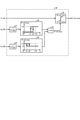
- FIG. 1 is a diagram showing a circuit configuration of a first embodiment of the MMC converter according to the present invention.
- FIG. 2 is a diagram showing a circuit configuration of an arm (positive side arm, negative side arm).
- FIG. 3 is a diagram showing a configuration of a power command suppression circuit according to the first embodiment.
- FIG. 4 is an explanatory diagram when a symmetry accident occurs in an AC system during operation in the modular multi-level power conversion system of the present invention.
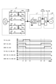
- FIG. 5 is a diagram showing a waveform when a symmetric accident occurs in power generation operation when the average voltage control output of all capacitors is used as an AC current effective component command but the active power command suppression circuit by positive phase voltage detection is not used. be.
- FIG. 6 is a diagram showing a waveform when a symmetric accident occurs in power generation operation when the average voltage control output of all capacitors is used as an effective component command of AC current and an active power command suppression circuit by positive phase voltage detection is used. ..
- FIG. 7 is an explanatory diagram when an asymmetric accident occurs in an AC system during operation in the modular multi-level power conversion system of the present invention.
- FIG. 8 shows a case where the average voltage control output of all capacitors is used as an AC current effective component command, only positive phase voltage detection is used for the active power command suppression circuit, and the active power command suppression circuit by reverse phase voltage detection is not used. It is a figure which shows the waveform at the time of the asymmetric accident occurrence in electric operation.
- FIG. 9 shows the case where an asymmetric accident occurs in electric operation when the average voltage control output of all capacitors is used as an AC current effective component command and an active power command suppression circuit by positive phase voltage detection and negative phase voltage detection is used together. It is a figure which shows the waveform.
- FIG. 10 is a diagram showing another configuration of the power command suppression circuit according to the first embodiment.
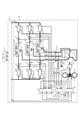
- FIG. 11 is a diagram showing a circuit configuration of a second embodiment of the MMC converter according to the present invention.
- FIG. 12 is a diagram showing the configuration of the current command suppression circuit according to the second embodiment.
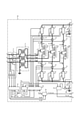
- FIG. 13 is a diagram showing a circuit configuration of a third embodiment of the variable speed motor generator according to the present invention.
- FIG. 14 is a diagram showing another circuit configuration of the third embodiment of the variable speed motor generator according to the present invention.
- FIG. 15 is a diagram showing a circuit configuration of an AC system side MMC converter constituting the variable speed motor generator of FIG. 14.
- FIG. 16 is a diagram showing a configuration of an active power control circuit according to a first embodiment and a third embodiment.
- FIG. 17 is a diagram showing the relationship between the capacity of the capacitor constituting the unit converter of the MMC converter and the voltage pulsation rate, the maximum voltage value, the average voltage value, and the minimum voltage value of the capacitor.
- FIG. 18 is a diagram showing the configuration of a conventional MMC converter.
- FIG. 19 is a diagram showing the relationship between the configuration of the upper control system of the conventional MMC converter and the present invention.
- FIG. 20 is a diagram showing another configuration of the upper control system of the conventional MMC converter.
- FIG. 21 is a diagram showing the correlation between the root squared average value and the arithmetic mean value for the one-period average value of the capacitor voltage constituting the unit converter of the MMC converter.
- FIG. 1 is a diagram showing a circuit configuration of a first embodiment of a modular multi-level power converter (hereinafter referred to as an MMC converter) according to the present invention.
- an MMC converter modular multi-level power converter
- FIG. 1 the components common to the MMC converter 60 shown in FIG. 18 described above are numbered the same. The components common to the MMC converter 60 will be omitted in order to avoid duplication.
- MMC converter which is connected to the AC system 2 via the unit transformer 4, and is connected to the DC power supply 3 at the DC side terminals (P, N).
- Reference numeral 10 is a current modifier, which detects the currents (IP_U, IP_V, IP_W, IN_U, IN_V, IN_W) of the 6 coils constituting the 3-terminal reactors 6U, 6V, 6W and outputs them to the converter current controller 11.
- FIG. 2 is a diagram showing a circuit configuration of an arm 7 (positive side arm 7UP, 7VP, 7WP, negative side arm 7UN, 7VN, 7WN).
- the arm 7 has a configuration in which K (K is a natural number) half bridge circuits 12 constituting a unit converter are connected in series between the first terminal A and the second terminal B.
- K K is a natural number
- FIG. 2 the description of the circuit configuration is omitted except for the half-bridge circuit 12 of “No. i”.
- the half-bridge circuit 12 includes two terminals, a positive terminal Y and a negative terminal X, and connects the self-arc extinguishing elements 13H and 13L and the antiparallel diodes 14H and 14L constituting the bidirectional chopper circuit to the capacitor 15.
- PWM control is performed based on the command from the converter current control device 11 so that the target voltage is output between the XY terminals by the firing / extinguishing command from the gate drive unit (GDU) 16H, 16L to the self-arc extinguishing elements 13H, 13L. ..
- Reference numeral 17 is a voltage detector, which outputs the voltage of the capacitor 15 to the capacitor voltage detector 21 via the signal converter (CONV) 18.
- the capacitor voltage detector 21 calculates the average value of the total number (6 ⁇ K) of the instantaneous voltage values of the capacitor, calculates the value Vc obtained by time-averaging the total number average value in one cycle of the AC system, and calculates the capacitor voltage regulator (AVcR). Output to 22.
- the capacitor voltage regulator (AVcR) 22 calculates an effective current command (Iq_ref) so that the capacitor voltage value Vc becomes a set value, and outputs it to the converter current control device 11.
- the AC signal calculator 19 inputs the voltage / current signal from the signal modifier 5 and calculates and outputs the active power (P_fB), the reactive power (Q_fB), and the positive phase voltage phase ( ⁇ p).
- the positive phase voltage phase ( ⁇ p) outputs a value converted to the second terminal side (U, V, W) according to the winding configuration of the unit transformer 4 and the phase order of the AC system 2.
- the output is advanced by 30 degrees with respect to the detection phase of the first terminal (AT, BT, CT).
- the AC signal calculator 19 calculates and outputs the positive phase voltage amplitude (Vp_fB) and the negative phase voltage amplitude (Vn_fB) of the AC system 2.
- Reference numeral 20 is a reactive power regulator (AQR), which calculates a reactive current command (Id_ref) so that the reactive power detection value (Q_fB) from the AC signal calculator 19 becomes a set value, and outputs the reactive current command (Id_ref) to the converter current controller 11. ..
- AQR reactive power regulator
- 23 is a DC power detector, which outputs the DC end active power (Pdc_fB) of the MMC converter 1.
- Reference numeral 24 denotes a switch, which selects the DC end active power (Pdc_fB) and the externally measured active power (Pac_fB) via the connection terminal S1 and outputs the DC active power regulator (APdcR) 25.
- the DC active power regulator (APdcR) 25 calculates a DC current command (Iz_ref) so that the detected value from the switch 24 becomes the set value (P_ref_mod), and outputs the DC current command (Iz_ref) to the converter current control device 11.
- the power command limiter 26 limits the active power command (P_ref) according to the positive phase voltage amplitude (Vp_fB) and the negative phase voltage amplitude (Vn_fB) from the AC signal calculator 19, and corrects the command (P_ref).
- P_ref_mod is output to the DC active power regulator (APdcR) 25.
- FIG. 3 is a diagram showing an embodiment of the power command limiter 26, in which the positive phase voltage amplitude (Vp_fB) is unitized by the rated voltage (V_rate) of the AC system 2 with a gain of 27 and input to the positive phase limiter 28. Similarly, the reverse phase voltage amplitude (Vn_fB) is unitized by the gain 29 and input to the reverse phase limiter 30.
- Vp_fB positive phase voltage amplitude
- V_rate the rated voltage
- Vn_fB the reverse phase voltage amplitude
- Reference numeral 31 is a low value selection circuit (LVG), in which the outputs of the positive phase limiter 28 and the negative phase limiter 30 are compared and selected, the limit value (P_ref_max) is output to the limiter 32, and the absolute power command (P_ref) is absolute. Suppress the value below the limit (P_ref_max).
- LVG low value selection circuit
- the positive phase limiter 28 has a configuration in which the output is limited to ⁇ when the unitized positive phase voltage amplitude is x1 or less, and the limit value is returned to the original 1.0 when it returns to x2 or more.
- This configuration has the effect of limiting the active power command reliably and stably in the event of a symmetric accident with a simple configuration.
- the reverse phase limiter 30 has a configuration in which the output is limited to ⁇ when the unitized reverse phase voltage amplitude is y2 or more, and the limit value is returned to the original 1.0 when it returns to y1 or less.
- This configuration has the effect of limiting the active power command reliably and stably, especially in the case of an asymmetrical accident that requires phase-open operation from the accident phase removal to the reclosing of the circuit, with a simple configuration.
- the behavior at the time of a system accident ripple differs depending on whether the system accident mode is a symmetric accident or an asymmetric accident.
- FIG. 4 shows the operating conditions when the MMC converter is connected to the trailing end of the two-line transmission line and a symmetric accident occurs in the AC system 2.
- the two-line transmission line is composed of a leading end circuit breaker 52F and a trailing end circuit breaker 52B.
- the three phases of the first line will be referred to as (1A, 1B, 1C)
- the three phases of the second line will be referred to as (2A, 2B, 2C).
- the DC side of two MMC converters is connected behind, one is connected to the AC system 2 via the unit transformer 4, and the AC side of the other MMC converter is connected to the AC rotating electric machine 40.
- the case where the variable speed power generation electric machine is configured by connecting with is shown.
- a three-phase ground fault occurs in the first line, and 73 is short-circuited.
- the leading end circuit breaker 52F and the trailing end circuit breaker 52B of the first line operate to open the circuit.
- the arc is extinguished at time t3 and 73 opens.
- the leading end circuit breaker 52F is reclosed at time t4, and the trailing end circuit breaker 52B is reclosed at time t5.
- FIGS. 5 and 6 compare the behavior during power generation operation.
- FIG. 5 shows the behavior at the time of the AC system accident spillover of FIG. 4 described above in the case where the power command limiter 26 of FIG. 3 is not provided in the configurations of FIGS. 1 and 2.
- the upper part of FIG. 5 is the value obtained by unitizing the active power (P_fB) and the active power (Q_fB) shown in FIG. 1 by the rated active power output of the MMC converter 1.
- the positive code is the time of supply.
- the direct current voltage (VDC) is a value obtained by unitizing the voltage value calculated from the differential of the current transformer 9 (9P, 9N) with a set value, and is a value before passing through the low frequency filter.
- FIG. 5 shows the rated operation time of the MMC converter 1 for both the active power (P_fB) and the active power (Q_fB).
- the rated power factor in this case is 0.85. Since the reference numeral is positive on the electric side, the active power (P_fB) is negative in the initial state of FIG.
- the middle part of FIG. 5 shows the value obtained by unitizing the phase voltage 3 signal on the first terminal side of the unit transformer 4 measured by the signal transformer 5 with the rated voltage of the unit transformer 4, and the detected current (IP_U) of the current transformer 10.
- IP_V, IP_W, IN_U, IN_V, IN_W The AC current (IAC_U, IAC_V, IAC_W) 3 signals on the 2nd terminal side of the unit transformer 4 are unitized by the rated value of the MMC converter 1. be.
- the lower part of FIG. 5 has a three-stage configuration, the upper part shows the U-phase of the MMC converter 1, the middle part shows the V-phase, and the lower part shows the instantaneous value of the capacitor voltage of the W-phase.
- the U phase will be described below.
- the K capacitor voltage signals constituting the positive arm (UP, VP, WP) instead of the K capacitor voltage signals constituting the positive arm (UP, VP, WP), the two signals of the maximum value (Vc_UPmax) and the minimum value (Vc_UPmin) of the 12 capacitors are aggregated.
- Vc_UNmax the maximum value
- Vc_UNmin the minimum value of the K capacitor voltages constituting the negative arm
- V phase and W phase are similarly represented by 4 signals each, but the description is omitted to avoid duplication.
- the largest bottleneck is the capacitor voltage shown in the lower part of Fig. 5.
- the rated voltage V0 of the capacitor voltage means the repetitive allowable voltage.
- the non-repeating allowable voltage is specified in the capacitor voltage rating.
- the capacitor voltage exceeds the allowable value before the time t2 when the leading end circuit breaker 52F and the trailing end circuit breaker 52B operate, and it is necessary to protect and stop the MMC converter 1.
- the sharp rise in the capacitor voltage is due to the reduction in the capacitor capacity in order to reduce the size of the MMC converter 1.
- the maximum value of the capacitor voltage is V0 even under exactly the same conditions as in FIG. It does not exceed 1.5 times.
- FIG. 6 shows the behavior at the time of the AC system accident spillover of FIG. 4 described above when the power command limiter 26 of FIG. 3 is used in the configuration of FIGS. 1 and 2 as in FIG.
- the waveforms displayed in the upper, middle, and lower waveforms of FIG. 6 and the display method are the same as those in the previous FIG. 5, and the description is omitted to avoid duplication.
- the capacitor voltage shown in the lower part of FIG. 6 is 1.5 times or less (about 1.2 times) the above-mentioned allowable voltage, and the equilibrium is maintained without the phenomenon that the maximum and minimum values of the capacitor voltage are opened.
- the MMC converter 1 can continue to operate stably even after the time t5 by the power command limiter 26.
- the reverse phase limiter 30 does not operate. Since the MMC converter 1 is directly connected to the loop transmission system, it is not necessary to assume a phase loss accident, or when the importance of power system operation is not strict and continuation of operation during open phase operation is not required. , The reverse phase voltage detection and the reverse phase limiter 30 are omitted, which has the effect of simplification.
- the behavior at the time of a system accident ripple differs depending on whether the system accident mode is a symmetric accident or an asymmetric accident.
- FIG. 7 shows the operating conditions when the MMC converter is connected to the trailing end of the two-line transmission line and an asymmetric accident accompanied by phase loss operation occurs in the AC system 2.
- variable speed power generation electric device is the same as that of the previous FIG. 4 by connecting to the AC rotating electric machine 40 of the above.
- a ground fault occurs at the same time in the 1A phase of the first line and the 2A phase of the second line, and 73 is short-circuited.
- the leading end circuit breaker 52F and the trailing end circuit breaker 52B of the first line operate to open the circuit.
- the arc is extinguished at time t3 and 73 opens.
- the leading end circuit breaker 52F is reclosed at time t4, and the trailing end circuit breaker 52B is reclosed at time t5.
- the MMC converter 1 is in a two-phase energized state of B phase and C phase (A phase open phase state).
- FIGS. 8 and 9 compare the behavior during the pumping operation.
- the behavior at the time of the AC system accident spillover is shown.
- FIG. 8 shows the rated operation time of the MMC converter 1 for both the active power (P_fB) and the active power (Q_fB).
- the rated power factor of this embodiment is 0.85.
- FIG. 8 is a plus sign for electric operation.
- the voltage balance begins to collapse after time t3, and the difference between the maximum value and the minimum value is large in the order of V phase, W phase, and U phase.
- the minimum value of both the P-side arm and the N-side arm is 0, and the stored energy is completely released.
- the maximum value is more than twice the maximum allowable value of the capacitor.
- the waveforms displayed in the upper, middle, and lower waveforms of FIG. 9 and the display method are the same as those in the previous FIG. 8, and the description thereof will be omitted in order to avoid duplication.
- the capacitor voltage shown in the lower part of FIG. 9 is 1.5 times or less (about 1.35 times) the above-mentioned allowable voltage, and the equilibrium is maintained without the phenomenon that the maximum and minimum values of the capacitor voltage are opened.
- the MMC converter 1 can continue to operate stably even after the phase open operation from time t2 to t5.
- FIG. 10 shows another embodiment of the reverse phase limiter 30 constituting the power command limiter 26.
- the output is limited to ⁇ 1 when the unitized reverse phase voltage amplitude is y2 or more, and is limited to ⁇ 2 when the unitized reverse phase voltage amplitude is y4 or more.
- the limit value is returned to ⁇ 1 when it returns to y1 or less, the limit value is returned to the original 1.
- the limit value of the power command can be adjusted in three stages according to the reverse phase voltage generation level, it is possible to suppress a decrease in active power.
- the MMC converter 1 when the MMC converter 1 is applied to an AC power generation motor, it has an effect of suppressing a speed decrease due to a decrease in active power during electric operation.
- the MMC converter 1 when applied to a variable speed pumped storage power generation system that drives a pump turbine, it has the effect of reducing the risk of falling into the backflow region of the pump turbine due to stall during the open phase operation period.
- FIG. 11 is a diagram showing a circuit configuration of the second embodiment of the MMC converter according to the present invention.
- the components common to the MMC converter 1 of the first embodiment shown in FIG. 1 are numbered the same.
- the components common to the MMC converter 1 will be omitted in order to avoid duplication.
- 34 is an MMC converter and 35 is a current command limiter.
- FIG. 12 is a diagram showing an embodiment of the current command limiter 35, in which the positive phase voltage amplitude (Vp_fB) is unitized by the rated voltage (V_rate) of the AC system 2 with a gain of 27 and input to the positive phase limiter 36. Similarly, the reverse phase voltage amplitude (Vn_fB) is unitized by the gain 29 and input to the reverse phase limiter 37.
- LVG low value selection circuit
- FIG. 13 is a diagram showing a circuit configuration of Example 3 relating to a variable speed power generation motor device using the MMC converter 1 and the MMC converter 39 according to the present invention.
- the components common to the MMC converter 1 of the first embodiment shown in FIG. 1 are numbered the same.
- the components common to the MMC converter 1 will be omitted in order to avoid duplication.
- Reference numeral 39 is an MMC converter, which is connected to the DC positive side terminal (P) and the negative side terminal (N) behind each other as the DC power supply of the MMC converter 1, and the AC terminal (R) of each phase of the AC rotating electric machine 40.
- S, T a 3-terminal reactor 6R, 6S, 6T is provided between the first terminal of the positive arm 7P and the second terminal of the negative arm 7N.
- Reference numeral 10 is a current modifier, which detects the currents (IP_R, IP_S, IP_T, IN_R, IN_S, IN_T) of the 6 coils constituting the 3-terminal reactors 6R, 6S, 6T and outputs them to the AC signal calculator 46.
- the armature neutral point of the AC rotating electric machine 40 is grounded via the high resistance 42.
- the pump turbine 43 is directly connected to the rotating shaft of the AC rotating electric machine 40.
- the pump turbine 43 has an open / close control function for the guide blades 44.
- Reference numeral 45 is a rotation phase detector, which outputs the phase ⁇ r of the rotation axis of the AC rotation electric machine 40 represented by the electric angle.
- Reference numeral 46 denotes an AC signal calculator, which inputs a voltage / current signal from the signal modifier 41 and a rotation phase ⁇ r, and performs so-called instantaneous active power (Pac_syn) and reactive power (Qac_syn) at regular time intervals according to the following equation (3).
- the phase voltage from the signal modifier 41 is (V_R, V_S, V_T)
- the current is (I_R, I_S, I_T).
- the phase order of the AC rotating electric machine 40 is R ⁇ S ⁇ T.
- the instantaneous active power (Pac_syn) and the active power (Qac_syn) are moved and averaged in one cycle of the rotation phase ( ⁇ r) from the rotation phase detector 45, and the active power (Pac_fB) and the ineffective power (Pac_fB) of the AC rotating electric machine 40.
- Qac_fB) is output.
- the active power (Pac_fB) signal is output to the above-mentioned DC active power regulator (APdcR) 25 via the above-mentioned switch 24 via the external terminal (S1) of the MMC converter 1. do.
- Reference numeral 211 is a capacitor voltage detector, which calculates the average value of all the instantaneous voltage values of the capacitor (6 ⁇ K), calculates the time-averaged value Vc of all the average values in one cycle of the rotation phase ( ⁇ r), and calculates the capacitor voltage. Output to the regulator (AVcR) 221.
- the reactive power regulator (AQR) 201 is an reactive power regulator (AQR), which realizes a power factor of 1 operation in order to minimize the current value of the AC rotating electric machine 40.
- the capacitor voltage regulator (AVcR) 221 calculates an effective current command (Iq_ref) so that the capacitor voltage value Vc becomes a set value, and outputs it to the converter current control device 47.
- the converter current controller 47 inputs the detected current (IP_R, IP_S, IP_T, IN_R, IN_S, IN_T) of the current transformer 10 from the alternating current (IAC_R, IAC_S, IAC_T) and the negative arm 7N of each phase.
- the through current (IPN_R, IPN_S, IPN_T) flowing through the positive arm 7P is calculated.
- the MMC converter 34 of the second embodiment shown in FIG. 11 may be used.
- FIG. 14 is a diagram showing a circuit configuration of Example 4 relating to a variable speed power generation motor device using the MMC converter 49 and the MMC converter 48 according to the present invention.
- the components common to the MMC converter 39 of the third embodiment shown in FIG. 13 are numbered the same.
- the components common to the MMC converter 39 will be omitted in order to avoid duplication.
- FIG. 15 shows an MMC converter 49 that constitutes a part of FIG.
- the components common to the MMC converter 1 of the first embodiment shown in FIG. 1 are numbered the same.
- the components common to the MMC converter 1 will be omitted in order to avoid duplication.
- the converter current controller 50 shown in FIG. 15 inputs the detected current (IP_U, IP_V, IP_W, IN_U, IN_V, IN_W) of the current transformer 10 and inputs the alternating current (IAC_U, IAC_V, IAC_W) and each phase.
- the through current (IPN_U, IPN_V, IPN_W) flowing from the negative arm 7N to the positive arm 7P is calculated.
- the DC power (Pdc_fB) detected by the DC power detector 23 is output to the MMC converter 48 in FIG. 14 via the external terminal (S2).
- the correction command (P_ref_mod) output from the power command limiter 26 is output to the MMC converter 48 in FIG. 14 via the external terminal (C1).
- 51 is a switch, which selects the AC flow end active power (Pac_fB) and the DC end active power (Pdc_fB) to be input via the connection terminal (S2), and adjusts the DC active power.
- Output to the device (APdcR) 52 is a switch, which selects the AC flow end active power (Pac_fB) and the DC end active power (Pdc_fB) to be input via the connection terminal (S2), and adjusts the DC active power.
- the DC active power regulator (APdcR) 52 calculates a DC current command (Iz_ref) so that the detected value from the switch 51 becomes a set value (P_ref_mod), and outputs the DC current command (Iz_ref) to the converter current control device 53.
- the converter current controller 53 inputs the detected current (IP_R, IP_S, IP_T, IN_R, IN_S, IN_T) of the current transformer 10 and inputs the alternating current (IAC_R, IAC_S, IAC_T) from the negative arm 7N of each phase.
- the through current (IPN_R, IPN_S, IPN_T) flowing through the positive arm 7P is calculated.
- FIG. 16 is a diagram showing a circuit configuration of a fifth embodiment of the MMC converter 54 according to the present invention.
- the components common to the MMC converter 1 of the first embodiment shown in FIG. 1 are numbered the same.
- the components common to the MMC converter 1 will be omitted in order to avoid duplication.
- Reference numeral 55 is an absolute value calculator, and is a difference signal in which the AC side active power Pac_fB input via the external terminal (S1) and the first terminal side active power P_fB of the unit transformer 4 detected by the AC signal calculator 19 are matched. Input d and output its absolute value e. As the AC side active power Pac_fB, the output of the AC signal calculator 46 described above is used.
- the set value e1 of the output switch 56 is set to a value larger than the input signal e during normal operation.
- the input signal e corresponds to the loss of the MMC converter connected behind the MMC converter 54.
- e1 is 0.1 times the rated active power of the MMC converter 54 and e2 is 0. Set to 05 times.
- the active power is controlled by the active power measured at the first terminal of the unit transformer 4, so that the active power command from the outside can be adjusted with high accuracy. Further, in the event of a system accident spread, the active power is controlled by the active power at the AC end of the AC rotating electric machine 40 or the like, which has the effect of stably continuing the operation of the MMC converter.
Landscapes
- Engineering & Computer Science (AREA)
- Power Engineering (AREA)
- Inverter Devices (AREA)
- Rectifiers (AREA)
Abstract
Description
特許文献2には、MMC変換器の基本的な制御構成が開示されている。
特許文献3には、MMC変換器を構成する単位変換器のコンデンサ電圧間の平衡を維持する方法が開示されている。
特許文献4には、直流側を背後接続した2台のMMC変換器のうちの1台の交流側を交流回転電気機械に接続して可変速発電電動装置を実現する方法が開示されている。
特許文献5には、実用的な上位制御装置の機能ブロック図が、明示的に示されている。

ここで、脈動率rは単位化した無次元数で
r=(Vc_max-Vc_min)/(Vc_max+Vc_min)
で定義している。
電圧Vc_max、Vc_ave、Vc_minはコンデンサ定格電圧V0で単位化した値を示す。
IAC_V=IP_V+IN_V
IAC_W=IP_W+IN_W
IPN_U=(1/2)×(IP_U-IN_U)
IPN_V=(1/2)×(IP_V-IN_V)
IPN_W=(1/2)×(IP_W-IN_W)
Pdc_fB=VDC_fB×IDC

IP_V_ref=(1/2)×IAC_V_ref+Iz_ref
IP_W_ref=(1/2)×IAC_W_ref+Iz_ref
IN_U_ref=(1/2)×IAC_U_ref-Iz_ref
IN_V_ref=(1/2)×IAC_V_ref-Iz_ref
IN_W_ref=(1/2)×IAC_W_ref-Iz_ref

IP_S_ref=(1/2)×IAC_S_ref+Iz_ref
IP_T_ref=(1/2)×IAC_T_ref+Iz_ref
IN_R_ref=(1/2)×IAC_R_ref-Iz_ref
IN_S_ref=(1/2)×IAC_S_ref-Iz_ref
IN_T_ref=(1/2)×IAC_T_ref-Iz_ref
2 交流系統
3 直流電源
4 ユニット変圧器
5,41 信号変成器
6,6U,6V,6W,6R,6S,6T 3端子リアクトル
7P,7UP,7VP,7WP 正側アーム
7N,7UN,7VN,7WN 負側アーム
8,8P,8N,42 高抵抗
9,9P,9N,10 電流変成器
11,47,50,53 変換器電流制御装置
12 ハーフブリッジ回路
13H,13L 自己消弧素子
14H,14L 逆並列ダイオード
15 コンデンサ
16H,16L ゲートドライブユニット
17 電圧検出器
18 信号変換器
19,46 交流信号演算器
20,70,201 無効電力調整器
21,211 コンデンサ電圧検出器
22,221 コンデンサ電圧調整器
23 直流電力検出器
24,51,59,69 切替器
25,52,67 直流有効電力調整器
26,電力指令制限器
27,29,57,58,64,65,75,76 利得
28,36 正相制限器
30,33,37 逆相制限器
31,38 低値選択回路
32,321 制限器
35 電流指令制限器
40 交流回転電気機械
43 ポンプ水車
44 案内羽根
45 回転位相検出器
55 絶対値演算器
56 出力切替器
61 MMC変換器エネルギー検出器
62 上位制御装置
63 変換器エネルギー調整器
66 交流有効電力調整器
71,72,73,74 スイッチ
Claims (4)
- 直流電源の正側端子(P端子)および負側端子(N端子)と交流系統の3相交流端子(U端子,V端子,W端子)間に接続されたモジュラー・マルチレベル電力変換器であって、K個(Kは1以上の自然数)の電圧源特性のエネルギー貯蔵要素を介して任意の電圧を出力可能な2端子の単位変換器を直列接続した2端子アームを、前記正側端子と前記3相交流端子間に3個(UPアーム,VPアーム,WPアーム)、前記負側端子と前記3相交流端子間に3個(UNアーム,VNアーム,WNアーム)備え、前記正側端子側の3個の2端子アームと前記負側端子側の3個の2端子アームと前記3相交流端子との間に2端子コイルを含む誘導素子と、前記正側端子側の3個のアームと前記負側端子側の3個のアームの電流を検出する6個のアーム電流変成器と、前記3相交流端子を流れる交流電流(IU,IV,IW)を検出あるいは演算する交流電流変成器と、前記3相交流端子の電圧変成器と、前記直流電源の正側端子を流れる電流(IDC)を検出あるいは演算する直流電流変成器と、前記交流電流変成器の信号から有効電流成分と無効電流成分を演算出力する交流電流演算器と、この有効電流成分と無効電流成分の演算出力が指令値に一致するように交流3相毎に交流電圧指令を演算して2分岐出力する交流電流調整器と、前記直流電流変成器からの電流信号と指令値が一致するように1個の直流電圧指令を演算して6分岐出力する直流電流調整器と、前記交流電圧指令と前記直流電圧指令を加減算して前記正側端子側の3個のアームと前記負側端子側の3個のアームを構成するパルス幅変調装置への変調率を出力する変調率演算器を備えたモジュラー・マルチレベル電力変換器において、
このモジュラー・マルチレベル電力変換器を構成する(6×k)個のコンデンサの平均電圧を検出・演算するコンデンサ平均電圧検出器と、このコンデンサ平均電圧検出値が指令値と一致するように前記交流電流調整器への有効電流成分指令を演算出力するコンデンサ電圧調整器と、前記交流電流変成器からの電流信号と交流電圧変成器からの電圧信号を入力して有効電力を演算出力する有効電力検出器と、この有効電力検出値と有効電力指令値が一致するように前記直流電流調整器への直流電流指令値を演算出力する有効電力調整器と、前記交流電圧変成器の3相電圧信号から正相電圧振幅を演算する正相電圧検出器と、この正相電圧振幅が第1設定値以下となると出力レベル0から1に、第2設定値以上になると出力レベル1から0に切り替える第1レベル検出器と、この第1レベル検出器の出力レベルが1の期間は前記直流電流調整器への有効電力指令値の絶対値を0あるいは定格直流電流の0.2倍以下の第1制限値に抑制する第1の有効電力指令抑制器と、前記交流電圧変成器の3相電圧信号から逆相電圧振幅を演算する逆相電圧検出器と、この逆相電圧振幅が第3設定値以上となると出力レベル0から1に、第4設定値以下になると出力レベル1から0に切り替える第2レベル検出器と、この第2レベル検出器の出力レベルが1の期間は前記直流電流調整器への有効電力指令値の絶対値を定格直流電流の0.3倍以上0.7倍以下の第2制限値に抑制する第2の有効電力指令抑制器と、を備えたことを特徴とするモジュラー・マルチレベル電力変換器。 - 直流電源の正側端子(P端子)および負側端子(N端子)と交流系統の3相交流端子(U端子,V端子,W端子)間に接続されたモジュラー・マルチレベル電力変換器であって、K個(Kは1以上の自然数)の電圧源特性のエネルギー貯蔵要素を介して任意の電圧を出力可能な2端子の単位変換器を直列接続した2端子アームを、前記正側端子と前記3相交流端子間に3個(UPアーム,VPアーム,WPアーム)、前記負側端子と前記3相交流端子間に3個(UNアーム,VNアーム,WNアーム)備え、前記正側端子側の3個の2端子アームと前記負側端子側の3個の2端子アームと前記3相交流端子との間に2端子コイルを含む誘導素子と、前記正側端子側の3個のアームと前記負側端子側の3個のアームの電流を検出する6個のアーム電流変成器と、前記3相交流端子を流れる交流電流(IU,IV,IW)を検出あるいは演算する交流電流変成器と、前記3相交流端子の電圧変成器と、前記直流電源の正側端子を流れる電流(IDC)を検出あるいは演算する直流電流変成器と、前記交流電流変成器の信号から有効電流成分と無効電流成分を演算出力する交流電流演算器と、この有効電流成分と無効電流成分の演算出力が指令値に一致するように交流3相毎に交流電圧指令を演算して2分岐出力する交流電流調整器と、前記直流電流変成器からの電流信号と指令値が一致するように1個の直流電圧指令を演算して6分岐出力する直流電流調整器と、前記交流電圧指令と前記直流電圧指令を加減算して前記正側端子側の3個のアームと前記負側端子側の3個のアームを構成するパルス幅変調装置への変調率を出力する変調率演算器を備えたモジュラー・マルチレベル電力変換器において、
このモジュラー・マルチレベル電力変換器を構成する(6×k)個のコンデンサの平均電圧を検出・演算するコンデンサ平均電圧検出器と、このコンデンサ平均電圧検出値が指令値と一致するように前記交流電流調整器への有効電流成分指令を演算出力するコンデンサ電圧調整器と、前記交流電流変成器からの電流信号と交流電圧変成器からの電圧信号を入力して有効電力を演算出力する有効電力検出器と、この有効電力検出値と有効電力指令値が一致するように前記直流電流調整器への直流電流指令値を演算出力する有効電力調整器と、前記交流電圧変成器の3相電圧信号から正相電圧振幅を演算する正相電圧検出器と、この正相電圧振幅が第1設定値以下となると出力レベル0から1に、第2設定値以上になると出力レベル1から0に切り替える第1レベル検出器と、この第1レベル検出器の出力レベルが1の期間は前記直流電流調整器からの直流電流指令値の絶対値を0あるいは定格直流電流の0.2倍以下の第1制限値に抑制する第1の直流電流指令抑制器と、前記交流電圧変成器の3相電圧信号から逆相電圧振幅を演算する逆相電圧検出器と、この逆相電圧振幅が第3設定値以上となると出力レベル0から1に、第4設定値以下になると出力レベル1から0に切り替える第2レベル検出器と、この第2レベル検出器の出力レベルが1の期間は前記直流電流調整器への直流電流指令値の絶対値を定格直流電流の0.3倍以上0.7倍以下の第2制限値に抑制する第2の直流電流指令抑制器と、を備えたことを特徴とするモジュラー・マルチレベル電力変換器。 - 前記コンデンサの交流系統周波数の電圧脈動率を(電圧最大値-電圧最小値)/(電圧最大値+電圧最小値)で定義し、この電圧脈動率が定格有効電力出力時に10%を超えることを特徴とする請求項1または2に記載のモジュラー・マルチレベル電力変換器。
- 請求項1または2に記載のモジュラー・マルチレベル電力変換器を第1のモジュラー・マルチレベル電力変換器とし、この直流端と背後接続した第2のモジュラー・マルチレベル電力変換器の交流端に交流回転電気機械を接続したことを特徴とする可変速発電電動装置。
Priority Applications (4)
| Application Number | Priority Date | Filing Date | Title |
|---|---|---|---|
| EP20954196.0A EP4216422A4 (en) | 2020-09-18 | 2020-09-18 | MODULAR MULTI-STAGE CURRENT CONVERTER AND VARIABLE SPEED ELECTRIC MOTOR/GENERATOR DEVICE |
| JP2022550327A JP7360559B2 (ja) | 2020-09-18 | 2020-09-18 | モジュラー・マルチレベル電力変換器および可変速発電電動装置 |
| US18/026,111 US12289063B2 (en) | 2020-09-18 | 2020-09-18 | Modular multilevel power converter and variable speed generator-motor |
| PCT/JP2020/035637 WO2022059211A1 (ja) | 2020-09-18 | 2020-09-18 | モジュラー・マルチレベル電力変換器および可変速発電電動装置 |
Applications Claiming Priority (1)
| Application Number | Priority Date | Filing Date | Title |
|---|---|---|---|
| PCT/JP2020/035637 WO2022059211A1 (ja) | 2020-09-18 | 2020-09-18 | モジュラー・マルチレベル電力変換器および可変速発電電動装置 |
Publications (1)
| Publication Number | Publication Date |
|---|---|
| WO2022059211A1 true WO2022059211A1 (ja) | 2022-03-24 |
Family
ID=80776779
Family Applications (1)
| Application Number | Title | Priority Date | Filing Date |
|---|---|---|---|
| PCT/JP2020/035637 Ceased WO2022059211A1 (ja) | 2020-09-18 | 2020-09-18 | モジュラー・マルチレベル電力変換器および可変速発電電動装置 |
Country Status (4)
| Country | Link |
|---|---|
| US (1) | US12289063B2 (ja) |
| EP (1) | EP4216422A4 (ja) |
| JP (1) | JP7360559B2 (ja) |
| WO (1) | WO2022059211A1 (ja) |
Cited By (2)
| Publication number | Priority date | Publication date | Assignee | Title |
|---|---|---|---|---|
| JPWO2024150437A1 (ja) * | 2023-01-13 | 2024-07-18 | ||
| JPWO2024154308A1 (ja) * | 2023-01-19 | 2024-07-25 |
Families Citing this family (2)
| Publication number | Priority date | Publication date | Assignee | Title |
|---|---|---|---|---|
| US12542437B2 (en) * | 2021-12-02 | 2026-02-03 | Tmeic Corporation | Reactive power control device, reactive power control method, and reactive power control program |
| KR102931812B1 (ko) * | 2023-06-08 | 2026-02-25 | 엘지전자 주식회사 | 영상표시장치 |
Citations (7)
| Publication number | Priority date | Publication date | Assignee | Title |
|---|---|---|---|---|
| JP4999930B2 (ja) | 2006-12-08 | 2012-08-15 | シーメンス アクチエンゲゼルシヤフト | 変換器の相モジュールにおける有効電力均衡の生成 |
| JP5189105B2 (ja) | 2006-12-08 | 2013-04-24 | シーメンス アクチエンゲゼルシヤフト | 電流変換装置 |
| JP5197623B2 (ja) | 2006-12-08 | 2013-05-15 | シーメンス アクチエンゲゼルシヤフト | エネルギー蓄積器が配分されたモジュール式コンバータ |
| WO2015178376A1 (ja) * | 2014-05-21 | 2015-11-26 | 三菱電機株式会社 | 直流送電電力変換装置および直流送電電力変換方法 |
| JP5993675B2 (ja) | 2012-09-14 | 2016-09-14 | 株式会社日立製作所 | 電力変換装置,電力変換システム及び電力変換装置の制御方法 |
| JP2017143626A (ja) * | 2016-02-09 | 2017-08-17 | 株式会社東芝 | 電力変換装置 |
| JP6243083B2 (ja) | 2015-02-25 | 2017-12-06 | 日立三菱水力株式会社 | 可変速発電電動装置および可変速発電電動システム |
Family Cites Families (2)
| Publication number | Priority date | Publication date | Assignee | Title |
|---|---|---|---|---|
| KR101809868B1 (ko) * | 2017-01-26 | 2018-01-18 | 엘에스산전 주식회사 | 무효전력보상장치 및 그 제어 방법 |
| JP6995991B2 (ja) * | 2018-06-07 | 2022-01-17 | 日立三菱水力株式会社 | 可変速発電電動装置 |
-
2020
- 2020-09-18 US US18/026,111 patent/US12289063B2/en active Active
- 2020-09-18 JP JP2022550327A patent/JP7360559B2/ja active Active
- 2020-09-18 WO PCT/JP2020/035637 patent/WO2022059211A1/ja not_active Ceased
- 2020-09-18 EP EP20954196.0A patent/EP4216422A4/en active Pending
Patent Citations (7)
| Publication number | Priority date | Publication date | Assignee | Title |
|---|---|---|---|---|
| JP4999930B2 (ja) | 2006-12-08 | 2012-08-15 | シーメンス アクチエンゲゼルシヤフト | 変換器の相モジュールにおける有効電力均衡の生成 |
| JP5189105B2 (ja) | 2006-12-08 | 2013-04-24 | シーメンス アクチエンゲゼルシヤフト | 電流変換装置 |
| JP5197623B2 (ja) | 2006-12-08 | 2013-05-15 | シーメンス アクチエンゲゼルシヤフト | エネルギー蓄積器が配分されたモジュール式コンバータ |
| JP5993675B2 (ja) | 2012-09-14 | 2016-09-14 | 株式会社日立製作所 | 電力変換装置,電力変換システム及び電力変換装置の制御方法 |
| WO2015178376A1 (ja) * | 2014-05-21 | 2015-11-26 | 三菱電機株式会社 | 直流送電電力変換装置および直流送電電力変換方法 |
| JP6243083B2 (ja) | 2015-02-25 | 2017-12-06 | 日立三菱水力株式会社 | 可変速発電電動装置および可変速発電電動システム |
| JP2017143626A (ja) * | 2016-02-09 | 2017-08-17 | 株式会社東芝 | 電力変換装置 |
Non-Patent Citations (2)
| Title |
|---|
| AHMED ZAMA, MODELING AND CONTROL OF MODULAR MULTILEVEL CONVERTERS(MMCS) FOR HVDC APPLICATIONS, November 2018 (2018-11-01), pages 111 |
| See also references of EP4216422A4 |
Cited By (6)
| Publication number | Priority date | Publication date | Assignee | Title |
|---|---|---|---|---|
| JPWO2024150437A1 (ja) * | 2023-01-13 | 2024-07-18 | ||
| WO2024150437A1 (ja) | 2023-01-13 | 2024-07-18 | 日立三菱水力株式会社 | モジュラー・マルチレベル電力変換器 |
| EP4651360A1 (en) | 2023-01-13 | 2025-11-19 | Hitachi Mitsubishi Hydro Corporation | Modular multilevel power converter |
| JPWO2024154308A1 (ja) * | 2023-01-19 | 2024-07-25 | ||
| WO2024154308A1 (ja) | 2023-01-19 | 2024-07-25 | 日立三菱水力株式会社 | モジュラー・マルチレベル電力変換器 |
| EP4654456A1 (en) | 2023-01-19 | 2025-11-26 | Hitachi Mitsubishi Hydro Corporation | Modular multi-level electric power converter |
Also Published As
| Publication number | Publication date |
|---|---|
| EP4216422A4 (en) | 2024-06-26 |
| US12289063B2 (en) | 2025-04-29 |
| JPWO2022059211A1 (ja) | 2022-03-24 |
| US20230369988A1 (en) | 2023-11-16 |
| EP4216422A1 (en) | 2023-07-26 |
| JP7360559B2 (ja) | 2023-10-12 |
Similar Documents
| Publication | Publication Date | Title |
|---|---|---|
| WO2022059211A1 (ja) | モジュラー・マルチレベル電力変換器および可変速発電電動装置 | |
| AU2008227057B2 (en) | Motor drive using flux adjustment to control power factor | |
| JP4501958B2 (ja) | 風力発電システムおよびその制御方法 | |
| US8896261B2 (en) | Doubly-fed generator and doubly-fed electric machine | |
| JP5542609B2 (ja) | 無効電力補償装置 | |
| CN104617584B (zh) | 一种全功率风电系统的电网故障穿越方法和装置 | |
| CN111769588A (zh) | 一种基于电网不平衡故障下vsg低电压穿越控制方法和系统 | |
| US11223310B2 (en) | Variable speed generator/motor device | |
| KR20110137378A (ko) | 전력변환장치의 제어방법 | |
| JP2002238163A (ja) | 電力変換装置 | |
| WO2014133026A1 (ja) | 速度センサレスモータ制御装置および速度センサレスモータ始動方法 | |
| JP4894906B2 (ja) | 風力発電システムの制御方法 | |
| WO2020013015A1 (ja) | 可変速発電電動装置 | |
| JP6448757B2 (ja) | インバータ制御方法 | |
| JP7012513B2 (ja) | 水力発電システム | |
| CN120109807B (zh) | 一种svi电网电压相位跳变下故障构网运行控制方法及系统 | |
| KR20180075282A (ko) | 고압인버터 전력셀의 직류단 전압 제어장치 | |
| EP2768134A1 (en) | Voltage control for a generator of a wind turbine | |
| JP2023067539A (ja) | 電力変換装置 | |
| WO2024154308A1 (ja) | モジュラー・マルチレベル電力変換器 | |
| JP7654089B2 (ja) | 一次可変速発電電動装置 | |
| Van Chung et al. | A New Model of Fault-Tolerant Predictive Current Control of Multilevel Cascaded H-Bridge Inverters for Induction Motors | |
| Choi et al. | Restarting strategy for an induction machine driven with medium-voltage inverter | |
| WO2024150437A1 (ja) | モジュラー・マルチレベル電力変換器 | |
| JP3312178B2 (ja) | 自励式インバータの制御装置 |
Legal Events
| Date | Code | Title | Description |
|---|---|---|---|
| 121 | Ep: the epo has been informed by wipo that ep was designated in this application |
Ref document number: 20954196 Country of ref document: EP Kind code of ref document: A1 |
|
| ENP | Entry into the national phase |
Ref document number: 2022550327 Country of ref document: JP Kind code of ref document: A |
|
| NENP | Non-entry into the national phase |
Ref country code: DE |
|
| ENP | Entry into the national phase |
Ref document number: 2020954196 Country of ref document: EP Effective date: 20230418 |
|
| WWG | Wipo information: grant in national office |
Ref document number: 18026111 Country of ref document: US |