WO2022065865A1 - 고효율 발광 소자, 그것을 갖는 유닛 픽셀, 및 그것을 갖는 디스플레이 장치 - Google Patents

고효율 발광 소자, 그것을 갖는 유닛 픽셀, 및 그것을 갖는 디스플레이 장치 Download PDF

Info

Publication number
WO2022065865A1
WO2022065865A1 PCT/KR2021/012934 KR2021012934W WO2022065865A1 WO 2022065865 A1 WO2022065865 A1 WO 2022065865A1 KR 2021012934 W KR2021012934 W KR 2021012934W WO 2022065865 A1 WO2022065865 A1 WO 2022065865A1
Authority
WO
WIPO (PCT)
Prior art keywords
layer
light emitting
type semiconductor
metal reflective
conductivity type
Prior art date
Legal status (The legal status is an assumption and is not a legal conclusion. Google has not performed a legal analysis and makes no representation as to the accuracy of the status listed.)
Ceased
Application number
PCT/KR2021/012934
Other languages
English (en)
French (fr)
Inventor
차남구
박연규
김상민
Current Assignee (The listed assignees may be inaccurate. Google has not performed a legal analysis and makes no representation or warranty as to the accuracy of the list.)
Seoul Viosys Co Ltd
Original Assignee
Seoul Viosys Co Ltd
Priority date (The priority date is an assumption and is not a legal conclusion. Google has not performed a legal analysis and makes no representation as to the accuracy of the date listed.)
Filing date
Publication date
Application filed by Seoul Viosys Co Ltd filed Critical Seoul Viosys Co Ltd
Priority to CN202180065547.8A priority Critical patent/CN116210094A/zh
Priority to JP2023518846A priority patent/JP7775299B2/ja
Priority to EP21872893.9A priority patent/EP4207320A4/en
Publication of WO2022065865A1 publication Critical patent/WO2022065865A1/ko
Anticipated expiration legal-status Critical
Ceased legal-status Critical Current

Links

Images

Classifications

    • HELECTRICITY
    • H10SEMICONDUCTOR DEVICES; ELECTRIC SOLID-STATE DEVICES NOT OTHERWISE PROVIDED FOR
    • H10HINORGANIC LIGHT-EMITTING SEMICONDUCTOR DEVICES HAVING POTENTIAL BARRIERS
    • H10H20/00Individual inorganic light-emitting semiconductor devices having potential barriers, e.g. light-emitting diodes [LED]
    • H10H20/80Constructional details
    • H10H20/81Bodies
    • H10H20/814Bodies having reflecting means, e.g. semiconductor Bragg reflectors
    • HELECTRICITY
    • H10SEMICONDUCTOR DEVICES; ELECTRIC SOLID-STATE DEVICES NOT OTHERWISE PROVIDED FOR
    • H10HINORGANIC LIGHT-EMITTING SEMICONDUCTOR DEVICES HAVING POTENTIAL BARRIERS
    • H10H20/00Individual inorganic light-emitting semiconductor devices having potential barriers, e.g. light-emitting diodes [LED]
    • H10H20/80Constructional details
    • H10H20/83Electrodes
    • H10H20/832Electrodes characterised by their material
    • H10H20/835Reflective materials
    • HELECTRICITY
    • H10SEMICONDUCTOR DEVICES; ELECTRIC SOLID-STATE DEVICES NOT OTHERWISE PROVIDED FOR
    • H10HINORGANIC LIGHT-EMITTING SEMICONDUCTOR DEVICES HAVING POTENTIAL BARRIERS
    • H10H20/00Individual inorganic light-emitting semiconductor devices having potential barriers, e.g. light-emitting diodes [LED]
    • H10H20/80Constructional details
    • H10H20/83Electrodes
    • H10H20/831Electrodes characterised by their shape
    • H10H20/8314Electrodes characterised by their shape extending at least partially onto an outer side surface of the bodies
    • HELECTRICITY
    • H10SEMICONDUCTOR DEVICES; ELECTRIC SOLID-STATE DEVICES NOT OTHERWISE PROVIDED FOR
    • H10HINORGANIC LIGHT-EMITTING SEMICONDUCTOR DEVICES HAVING POTENTIAL BARRIERS
    • H10H20/00Individual inorganic light-emitting semiconductor devices having potential barriers, e.g. light-emitting diodes [LED]
    • H10H20/80Constructional details
    • H10H20/85Packages
    • H10H20/855Optical field-shaping means, e.g. lenses
    • H10H20/856Reflecting means
    • HELECTRICITY
    • H10SEMICONDUCTOR DEVICES; ELECTRIC SOLID-STATE DEVICES NOT OTHERWISE PROVIDED FOR
    • H10HINORGANIC LIGHT-EMITTING SEMICONDUCTOR DEVICES HAVING POTENTIAL BARRIERS
    • H10H20/00Individual inorganic light-emitting semiconductor devices having potential barriers, e.g. light-emitting diodes [LED]
    • H10H20/80Constructional details
    • H10H20/85Packages
    • H10H20/857Interconnections, e.g. lead-frames, bond wires or solder balls
    • HELECTRICITY
    • H10SEMICONDUCTOR DEVICES; ELECTRIC SOLID-STATE DEVICES NOT OTHERWISE PROVIDED FOR
    • H10HINORGANIC LIGHT-EMITTING SEMICONDUCTOR DEVICES HAVING POTENTIAL BARRIERS
    • H10H29/00Integrated devices, or assemblies of multiple devices, comprising at least one light-emitting semiconductor element covered by group H10H20/00
    • H10H29/80Constructional details
    • H10H29/85Packages
    • H10H29/855Optical field-shaping means, e.g. lenses
    • H10H29/8552Light absorbing arrangements, e.g. black matrix
    • HELECTRICITY
    • H10SEMICONDUCTOR DEVICES; ELECTRIC SOLID-STATE DEVICES NOT OTHERWISE PROVIDED FOR
    • H10WGENERIC PACKAGES, INTERCONNECTIONS, CONNECTORS OR OTHER CONSTRUCTIONAL DETAILS OF DEVICES COVERED BY CLASS H10
    • H10W90/00Package configurations
    • HELECTRICITY
    • H10SEMICONDUCTOR DEVICES; ELECTRIC SOLID-STATE DEVICES NOT OTHERWISE PROVIDED FOR
    • H10HINORGANIC LIGHT-EMITTING SEMICONDUCTOR DEVICES HAVING POTENTIAL BARRIERS
    • H10H20/00Individual inorganic light-emitting semiconductor devices having potential barriers, e.g. light-emitting diodes [LED]
    • H10H20/80Constructional details
    • H10H20/84Coatings, e.g. passivation layers or antireflective coatings
    • H10H20/841Reflective coatings, e.g. dielectric Bragg reflectors

Definitions

  • Exemplary embodiments relate to a micro LED display device, and more particularly, to a high-efficiency light-emitting element, a unit pixel having the same, and a display device having the same.
  • a light emitting device is a semiconductor device using a light emitting diode, which is an inorganic light source, and is used in various fields such as display devices, vehicle lamps, and general lighting.
  • Light emitting diodes have long lifespan, low power consumption, and fast response speed, so they are rapidly replacing existing light sources.
  • a conventional light emitting diode has been mainly used as a backlight light source in a display device.
  • a display device that directly implements an image using a light emitting diode has been developed. Such displays are also referred to as micro LED displays.
  • a display device generally implements various colors by using a mixture of blue, green, and red colors.
  • a display device includes a plurality of pixels to implement various images, and each pixel includes blue, green, and red sub-pixels. A color of a specific pixel is determined through the color of these sub-pixels, and an image is implemented by a combination of these pixels.
  • Exemplary embodiments provide a micro-scale light emitting device with improved light efficiency.
  • Exemplary embodiments provide a light emitting module manufacturing method suitable for mass production, in which a unit pixel employing high-efficiency light emitting devices, and/or a transparent molding unit can be easily implemented.
  • An exemplary embodiment provides a micro-scale light emitting device, the light emitting device comprising a first conductivity type semiconductor layer, a second conductivity type semiconductor layer, and disposed between the first conductivity type semiconductor layer and the second conductivity type semiconductor layer a semiconductor stack including an active layer; an insulating layer covering an upper surface and a side surface of the semiconductor stack; and a metal reflective layer disposed on the insulating layer and covering at least a portion of a side surface of the semiconductor stack, wherein the insulating layer includes a distributed Bragg reflector.
  • An exemplary embodiment provides a micro-scale light emitting device, the light emitting device comprising a first conductivity type semiconductor layer, a second conductivity type semiconductor layer, and disposed between the first conductivity type semiconductor layer and the second conductivity type semiconductor layer a semiconductor stack including an active layer; an insulating layer covering an upper surface and a side surface of the semiconductor stack; and a metal reflective layer disposed on the insulating layer and covering at least a portion of a side surface of the semiconductor stack, wherein the thickness of the insulating layer disposed on the upper surface of the semiconductor stack is the thickness of the insulating layer disposed on the side of the semiconductor stack. larger than
  • An exemplary embodiment provides a unit pixel, the unit pixel comprising: a transparent substrate; a light blocking layer disposed on the transparent substrate and having windows that transmit light; and a plurality of light emitting devices disposed on the light blocking layer to be aligned with the windows, wherein each of the light emitting devices includes a first conductivity type semiconductor layer, a second conductivity type semiconductor layer, and a first conductivity type semiconductor layer; a semiconductor stack including an active layer disposed between second conductivity-type semiconductor layers; an insulating layer covering an upper surface and a side surface of the semiconductor stack; and a metal reflective layer disposed on the insulating layer and covering at least a portion of a side surface of the semiconductor stack, wherein the insulating layer includes a distributed Bragg reflector.
  • An exemplary embodiment provides a display device comprising: a circuit board; unit pixels mounted on the circuit board; and a molding unit covering the unit pixels, wherein the unit pixels include a transparent substrate and a plurality of light emitting devices disposed on the transparent substrate, wherein the light emitting devices are each of a first conductivity type semiconductor layer and a second conductivity type a semiconductor stack comprising a semiconductor layer and an active layer disposed between the first conductivity-type semiconductor layer and the second conductivity-type semiconductor layer; an insulating layer covering an upper surface and a side surface of the semiconductor stack; and a metal reflective layer disposed on the insulating layer and covering at least a portion of a side surface of the semiconductor stack, wherein the insulating layer includes a distributed Bragg reflector.
  • Fig. 1B is a schematic cross-sectional view taken along line A-A' of Fig. 1A;
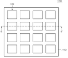
  • 2A is a schematic plan view for explaining a light emitting module according to an embodiment.
  • 3A is a schematic plan view illustrating a unit pixel according to an exemplary embodiment.
  • Fig. 3B is a schematic cross-sectional view taken along line C-C' of Fig. 3A;
  • 4A is a schematic plan view for explaining a light emitting device according to an embodiment.
  • Fig. 4B is a schematic cross-sectional view taken along line D-D' of Fig. 4A;
  • 5A is a schematic plan view for explaining a light emitting device according to another embodiment.
  • 5B is a schematic plan view for explaining a light emitting device according to another embodiment.
  • a light emitting device is a micro-scale light emitting device, and includes a first conductivity type semiconductor layer, a second conductivity type semiconductor layer, and an active layer disposed between the first conductivity type semiconductor layer and the second conductivity type semiconductor layer.
  • a semiconductor stack comprising; an insulating layer covering an upper surface and a side surface of the semiconductor stack; and a metal reflective layer disposed on the insulating layer and covering at least a portion of a side surface of the semiconductor stack, wherein the insulating layer includes a distributed Bragg reflector.
  • the micro-scale light emitting device has a size generally used for a micro LED display.
  • the micro-scale light emitting device may have a length of, for example, a long axis of 200 ⁇ m or less, and further, may have a size of 100 ⁇ m or less.
  • a thickness of the insulating layer covering an upper surface of the semiconductor stack may be greater than a thickness of the insulating layer covering a side surface of the semiconductor stack.
  • the insulating layer covering the upper surface of the semiconductor stack may have a higher reflectance than the insulating layer covering the side surface of the semiconductor stack.
  • the metal reflective layer may include a first metal reflective layer and a second metal reflective layer spaced apart from each other, and the first and second metal reflective layers may partially cover a side surface of the semiconductor stack, respectively.
  • the light emitting device may further include a first electrode pad and a second electrode pad disposed on the insulating layer and electrically connected to the first conductivity type semiconductor layer and the second conductivity type semiconductor layer, respectively, A first metal reflective layer may cover the first electrode pad, and the second metal reflective layer may cover the second electrode pad.
  • the metal reflective layer may be spaced apart from the first and second electrode pads.
  • the metal reflective layer may cover the first electrode pad and may be spaced apart from the second electrode pad.
  • the insulating layer disposed on the upper surface of the semiconductor stack may have a higher reflectance than the insulating layer disposed on the side surface of the semiconductor stack.
  • a unit pixel includes a transparent substrate; a light blocking layer disposed on the transparent substrate and having windows that transmit light; and a plurality of light emitting devices disposed on the light blocking layer to be aligned with the windows, wherein each of the light emitting devices includes a first conductivity type semiconductor layer, a second conductivity type semiconductor layer, and a first conductivity type semiconductor layer; a semiconductor stack including an active layer disposed between second conductivity-type semiconductor layers; an insulating layer covering an upper surface and a side surface of the semiconductor stack; and a metal reflective layer disposed on the insulating layer and covering at least a portion of a side surface of the semiconductor stack, wherein the insulating layer includes a distributed Bragg reflector.
  • the metal reflective layer may include a first metal reflective layer and a second metal reflective layer spaced apart from each other.
  • the molding part 1003 covers the unit pixels 100 .
  • the molding part 1003 may be in contact with the surface of the circuit board 1001 and may also cover upper surfaces of the unit pixels 100 .
  • the molding part 1003 may have a flat top surface. In particular, unlike the prior art, a recess is not formed on the area between the unit pixels 100 .
  • the anti-glare layer 1005 may cover the molding part 1003 .
  • the anti-glare layer 1005 reduces the user's eye fatigue by preventing light reflection.
  • the anti-glare layer 1005 may be formed by, for example, mixing fine particles such as silica, melamine, acrylic, etc. with a cured resin to form an ink, and coating the surface of the molding part 1003 to be cured using ultraviolet rays. can
  • the unit pixels 100 are formed of the light emitting module 1000 , and the plurality of light emitting modules 1000 are mounted on the panel substrate 2100 to provide the display device 10000 , , thus, the process yield of the display apparatus 10000 may be improved.
  • the unit pixel 100 provides one pixel including the first to third light emitting elements 10a, 10b, and 10c.
  • the first to third light emitting devices 10a , 10b , and 10c emit light of different colors, which respectively correspond to sub-pixels.
  • the transparent substrate 121 is a light-transmitting substrate such as PET, a glass substrate, a quartz substrate, or a sapphire substrate.
  • the transparent substrate 121 is disposed on the light emitting surface of the light emitting module 1000 , and the light emitted from the light emitting devices 10a , 10b and 10c is emitted to the outside through the transparent substrate 121 .
  • the transparent substrate 121 may have an upper surface and a lower surface.
  • the transparent substrate 121 may include a concave-convex pattern 121p on a surface that faces the light emitting elements 10a, 10b, and 10c, that is, an upper surface.
  • the uneven pattern 121p may be regular or irregular.
  • the uneven pattern 121p may have, for example, a pitch of 3 ⁇ m, a diameter of 2.8 ⁇ m, and a height of 1.8 ⁇ m.
  • the concave-convex pattern 121p may be a pattern generally applied to a patterned sapphire substrate, but is not limited thereto.
  • the transparent substrate 121 Since the transparent substrate 121 is disposed on the light emitting surface, the transparent substrate 121 does not include a circuit. However, the present disclosure is not limited thereto, and may include a circuit.
  • the adhesive layer 125 may be formed as a light-transmitting layer, and transmits light emitted from the light emitting devices 10a, 10b, and 10c.
  • the adhesive layer 125 may be formed using an organic adhesive.
  • the adhesive layer 125 may be formed using a transparent epoxy.
  • the adhesive layer 125 may include a diffuser such as SiO 2 , TiO 2 , or ZnO to diffuse light.
  • the light diffusing material prevents the light emitting elements 10a, 10b, 10c from being viewed from the light emitting surface.
  • the step control layer 127 covers the first to third light emitting devices 10a, 10b, and 10c.
  • the step control layer 127 has openings 127a exposing electrode pads of the light emitting devices 10a, 10b, and 10c.
  • the step control layer 127 helps to safely form the connection layers by constantly adjusting the height of the surface on which the connection layers 129a, 129b, 129c, and 129d are formed.
  • the step control layer 127 may be formed of, for example, photosensitive polyimide.
  • the step control layer 127 may be disposed in a region surrounded by an edge of the adhesive layer 125 , but is not limited thereto.
  • the step control layer 127 may be formed to partially expose an edge of the adhesive layer 125 .
  • the first to fourth connection layers 129a, 129b, 129c, and 129d may be formed together on the step control layer 127 and may have a single layer or multiple layers.
  • it may include at least one of Cr, Ti, Ni, Cu, Al, Pt, and Au.
  • the insulating material layer 131 covers the side surfaces of the step control layer 127 and the connection layers 129a, 129b, 129c, and 129d. Also, the insulating material layer 131 may cover a portion of the adhesive layer 125 .
  • the insulating material layer 131 has openings 131a, 131b, 131c, and 131d exposing the connection layers 129a, 129b, 129c, and 129d, so that pad regions of the unit pixel 100 can be defined. there is.
  • the insulating material layer 131 may be a translucent material, and may be formed of an organic or inorganic material.
  • the insulating material layer 131 may be formed of, for example, polyimide.
  • the connection layers 129a, 129b, 129c, and 129d have a lower surface, a side surface, and an upper surface except for pad regions. All may be surrounded by polyimide.
  • the unit pixel 100 may be mounted on the circuit board using a bonding material such as solder, and the bonding material is the connection layer exposed to the openings 131a, 131b, 131c, and 131d of the insulating material layer 131 . (129a, 129b, 129c, 129d) and pads on the circuit board may be bonded.
  • a bonding material such as solder
  • the unit pixel 100 does not include separate bumps, and the connection layers 129a, 129b, 129c, and 129d are used as bonding pads.
  • the present invention is not limited thereto, and bonding pads covering the openings 131a, 131b, 131c, and 131d of the insulating material layer 131 may be formed.
  • the first to fourth connection layers 129a, 129b, 129c, and 129d may be formed to partially cover the light emitting devices 10a, 10b, and 10c outside the upper region thereof.
  • the adhesive layer 125 described above is also an example of an optical layer.
  • the optical layer is formed of a material different from that of the light-emitting elements 10a, 10b, and 10c, for example, gas, liquid, or solid, and thus the material of the semiconductor layers in the light-emitting elements 10a, 10b, 10c and distinguished
  • the unit pixel 100 in which the light emitting elements 10a, 10b, and 10c are arranged on the same plane is provided.
  • the unit pixel 100 may implement light of various colors using the light emitting elements 10a, 10b, and 10c.
  • the light emitting devices 10a, 10b, and 10c according to an embodiment will be described in detail.
  • FIG. 4A is a schematic plan view for explaining a light emitting device 10a according to an embodiment of the present disclosure
  • FIG. 4B is a schematic cross-sectional view taken along the cut-out line D-D' of FIG. 4A.
  • the light emitting device 10a is described as an example, but since the light emitting devices 10b and 10c also have substantially similar structures, descriptions overlapping each other will be omitted.
  • the light emitting device 10a is a light emitting structure including a first conductivity type semiconductor layer 21, an active layer 23, and a second conductivity type semiconductor layer 25, an ohmic contact layer ( 27), a first contact pad 53, a second contact pad 55, an insulating layer 59, a first electrode pad 61, a second electrode pad 63, a first reflective metal layer 65a, and A second reflective metal layer 65b may be included.
  • the light emitting structure that is, the first conductivity type semiconductor layer 21 , the active layer 23 , and the second conductivity type semiconductor layer 25 may be grown on the substrate.
  • the substrate may be a variety of substrates that can be used for semiconductor growth, such as a gallium nitride substrate, a GaAs substrate, a Si substrate, a sapphire substrate, particularly a patterned sapphire substrate.
  • the growth substrate may be separated from the semiconductor layers using techniques such as mechanical polishing, laser lift-off, and chemical lift-off.
  • the present invention is not limited thereto, and a portion of the substrate may remain to constitute at least a portion of the first conductivity-type semiconductor layer 21 .
  • the semiconductor layers include aluminum gallium arsenide (AlGaAs), gallium arsenide phosphide (GaAsP), and aluminum gallium indium phosphide (aluminum gallium). indium phosphide, AlGaInP), or gallium phosphide (GaP).
  • the semiconductor layers are indium gallium nitride (InGaN), gallium nitride (GaN), gallium phosphide (GaP), aluminum gallium indium phosphide (AlGaInP), or aluminum gallium phosphide (AlGaP).
  • InGaN indium gallium nitride
  • GaN gallium nitride
  • GaP gallium phosphide
  • AlGaInP aluminum gallium indium phosphide
  • AlGaP aluminum gallium phosphide
  • the semiconductor layer may include gallium nitride (GaN), indium gallium nitride (InGaN), or zinc selenide (ZnSe).
  • GaN gallium nitride
  • InGaN indium gallium nitride
  • ZnSe zinc selenide
  • the first conductivity type and the second conductivity type have opposite polarities.
  • the first conductivity type is n-type
  • the second conductivity type is p-type
  • the first conductivity type is p-type
  • the second conductivity type is n-type do.
  • the first conductivity type semiconductor layer 21 , the active layer 23 , and the second conductivity type semiconductor layer 25 may be grown on a substrate in a chamber using a known method such as metal organic chemical vapor deposition (MOCVD).
  • MOCVD metal organic chemical vapor deposition
  • the first conductivity-type semiconductor layer 21 includes n-type impurities (eg, Si, Ge, Sn)
  • the second conductivity-type semiconductor layer 25 includes p-type impurities (eg, Mg, Sr, Ba).
  • the first conductivity type semiconductor layer 21 may include GaN or AlGaN including Si as a dopant
  • the second conductivity type semiconductor layer 25 may include GaN or AlGaN including Mg as a dopant. may include
  • the active layer 23 may include a single quantum well structure or a multi-quantum well structure, and the composition ratio of the nitride-based semiconductor is adjusted to emit a desired wavelength.
  • the active layer 23 may emit blue light, green light, red light, or ultraviolet light.
  • the second conductivity type semiconductor layer 25 and the active layer 23 may have a mesa (M) structure and be disposed on the first conductivity type semiconductor layer 21 .
  • the mesa M includes the second conductivity type semiconductor layer 25 and the active layer 23 , and may include a part of the first conductivity type semiconductor layer 21 as shown in FIG. 4B .
  • the mesa M is positioned on a partial region of the first conductivity type semiconductor layer 21 , and a top surface of the first conductivity type semiconductor layer 21 may be exposed around the mesa M .
  • the mesa M is formed to expose the first conductivity type semiconductor layer 21 around the mesa.
  • a through hole may be formed through the mesa M to expose the first conductivity-type semiconductor layer 21 .
  • cone-shaped protrusions may be formed, the height of the cone may be 2 to 3um, the cone interval may be 1.5 to 2um, and the bottom diameter of the cone may be about 3um to 5um.
  • the cone may also be truncated, in which case the top surface diameter of the cone may be about 2-3 um.
  • the concavo-convex pattern 21p may include a first concavo-convex pattern and a second concavo-convex pattern additionally formed on the first concavo-convex pattern.
  • the second concave-convex pattern may be formed to have a smaller size than that of the first concave-convex pattern.
  • At least one of the first conductivity-type semiconductor layers 21 of the light emitting devices 10a, 10b, and 10c may have an inclined side surface as shown in FIG. 4B .
  • the inclined side surface of the first conductivity type semiconductor layer 21 may be formed by a device isolation process.
  • the inclination angle of the side surface of the first conductivity type semiconductor layer 21 may be in the range of about 40 to about 80 degrees with respect to the bottom surface of the first conductivity type semiconductor layer 21 .
  • the mesa (M) may also have an inclined side, and may range from about 40 to about 80 degrees with respect to the bottom surface of the mesa (M).
  • metal reflective layers 65a and 65b to be described later may be easily formed.
  • the first contact pad 53 is disposed on the exposed first conductivity type semiconductor layer 21 .
  • the first contact pad 53 may be in ohmic contact with the first conductivity type semiconductor layer 21 .
  • the first contact pad 53 may be formed of an ohmic metal layer in ohmic contact with the first conductivity-type semiconductor layer 21 .
  • the ohmic metal layer of the first contact pad 53 may be appropriately selected according to the semiconductor material of the first conductivity type semiconductor layer 21 .
  • the first contact pad 53 may be omitted.
  • the insulating layer 59 covers the mesa M, the ohmic contact layer 27 , the first contact pad 53 , and the second contact pad 55 .
  • the insulating layer 59 has openings 59a and 59b exposing the first contact pad 53 and the second contact pad 55 .
  • the insulating layer 59 may include a distributed Bragg reflector in which insulating layers having different refractive indices are stacked.
  • the distributed Bragg reflector may include at least two insulating layers selected from SiO 2 , Si 3 N 4 , SiON, TiO 2 , Ta 2 O 5 , Nb 2 O 5 , MgF 2 , and the like.
  • distributed Bragg reflectors applied to the red, green, and blue light emitting devices 10a, 10b, and 10c may have substantially similar thicknesses.
  • the thickness difference between the distributed Bragg reflectors applied to these light emitting elements 10a, 10b, 10c may be less than 10% of the thickness of the thickest distributed Bragg reflector.
  • the process conditions applied to the red, green, and blue light emitting devices 10a, 10b, and 10c, for example, the process of patterning the insulating layer 59 can be set similarly, , furthermore, it is possible to prevent the unit pixel manufacturing process from becoming complicated.
  • distributed Bragg reflectors applied to the red, green, and blue light emitting elements 10a, 10b, and 10c may have substantially similar stacking numbers.
  • the present invention is not limited thereto.
  • the first and/or second electrode pads 61 and 63 may be formed of a single layer or a multi-layered metal.
  • metals such as Al, Ti, Cr, Ni, Au, and alloys thereof may be used.
  • the thickness of the insulating layer 59 formed on the side surface of the mesa M and the side surface of the first conductivity type semiconductor layer 21 is the second conductivity type semiconductor layer. (25) will be smaller than the thickness of the insulating layer 59 formed thereon. That is, the insulating layer 59 formed on the side surface of the light emitting element 10a is relatively thinner than the insulating layer 59 formed on the upper surface.
  • the first and second metal reflective layers 65a and 65b may form an omni-directional reflector together with the insulating layer 59 , thereby preventing light leakage and increasing light efficiency in the light emission direction.
  • the first metal reflective layer 65a may cover the first electrode pad 61 , and may cover a side surface of the light emitting device 10a around the first electrode pad 61 . As shown in FIG.
  • the first metal reflective layer 65a and the second metal reflective layer 65b are spaced apart from each other to prevent an electrical short circuit.
  • the separation distance between the first metal reflective layer 65a and the second metal reflective layer 65b may be closer than the separation distance between the first electrode pad 61 and the second electrode pad 63 , but is not limited thereto.
  • the first metal reflective layer 65a and the second metal reflective layer 65b may include Cr, Ni, Al, Pt, Ag, or Au.
  • the metal reflective layer 165 is disposed in a ring shape along the side surface of the light emitting device, and is spaced apart from the first and second electrode pads 61 and 63 .
  • the metal reflective layer 165 covers side surfaces of the first conductivity type semiconductor layer 21 , the active layer 23 , and the second conductivity type semiconductor layer 25 .
  • 5B is a schematic plan view for explaining a light emitting device according to another embodiment.
  • the first and second metal reflective layers 65a and 65b may be safely formed on the light emitting devices arranged at narrow intervals.

Landscapes

  • Led Devices (AREA)
  • Led Device Packages (AREA)
  • Devices For Indicating Variable Information By Combining Individual Elements (AREA)

Abstract

일 실시예에 따른 발광 소자는, 마이크로 스케일의 발광 소자로서, 제1 도전형 반도체층, 제2 도전형 반도체층, 및 제1 도전형 반도체층과 제2 도전형 반도체층 사이에 배치된 활성층을 포함하는 반도체 적층; 상기 반도체 적층의 상면 및 측면을 덮는 절연층; 및 상기 절연층 상에 배치되며, 상기 반도체 적층의 측면의 적어도 일부를 덮는 금속 반사층을 포함하고, 상기 절연층은 분포 브래그 반사기를 포함한다.

Description

고효율 발광 소자, 그것을 갖는 유닛 픽셀, 및 그것을 갖는 디스플레이 장치
예시적인 실시예들은 마이크로 LED 디스플레이 장치에 관한 것으로, 특히, 고효율 발광 소자, 그것을 갖는 유닛 픽셀, 및 그것을 갖는 디스플레이 장치에 관한 것이다.
발광소자는 무기 광원인 발광 다이오드를 이용한 반도체 소자로, 디스플레이 장치, 차량용 램프, 일반 조명과 같은 여러 분야에 다양하게 이용되고 있다. 발광 다이오드는 수명이 길고, 소비전력이 낮으며, 응답속도가 빠른 장점이 있어 기존 광원을 빠르게 대체하고 있다.
한편, 종래의 발광 다이오드는 디스플레이 장치에서 백라이트 광원으로 주로 사용되었는데, 최근 발광 다이오드를 이용하여 직접 이미지를 구현하는 디스플레이 장치가 개발되고 있다. 이러한 디스플레이는 마이크로 LED 디스플레이로 지칭되기도 한다.
디스플레이 장치는 일반적으로 청색, 녹색 및 적색의 혼합 색을 이용하여 다양한 색상을 구현한다. 디스플레이 장치는 다양한 이미지를 구현하기 위해 복수의 픽셀을 포함하고, 각 픽셀은 청색, 녹색 및 적색의 서브 픽셀을 구비한다. 이들 서브 픽셀들의 색상을 통해 특정 픽셀의 색상이 정해지고, 이들 픽셀들의 조합에 의해 이미지가 구현된다.
마이크로 LED 디스플레이의 경우, 각 서브 픽셀에 대응하여 마이크로 LED가 2차원 평면상에 배열되고, 이에 따라 하나의 기판 상에 수많은 개수의 마이크로 LED가 배치될 필요가 있다. 그런데 마이크로 LED는 그 크기가 예컨대 200 마이크로미터 이하, 나아가 100 마이크로미터 이하로 대단히 작으며, 이러한 작은 크기로 인해 다양한 문제점이 발생한다. 특히, 작은 크기의 발광 다이오드를 핸들링하는 것이 어려워 디스플레이 기판 상에 발광 다이오드를 직접 실장하는 것이 용이하지 않다.
한편, 마이크로 LED에서 생성된 광 중 상당 부분이 외부로 방출되지 못하고 손실되며, 이에 따라, 마이크로 LED의 광 효율이 일반 LED에 비해 상대적으로 낮다. 따라서, 마이크로 LED의 광 효율을 개선할 필요가 있다.
예시적인 실시예들은 광 효율이 개선된 마이크로 스케일의 발광 소자를 제공한다.
예시적인 실시예들은 고효율 발광 소자들을 채택한 유닛 픽셀, 및 또는 투명 몰딩부를 쉽게 구현할 수 있으며, 대량 생산에 적합한 발광 모듈 제조 방법을 제공한다.
예시적인 실시예는 마이크로 스케일의 발광 소자를 제공하는데, 이 발광 소자는, 제1 도전형 반도체층, 제2 도전형 반도체층, 및 제1 도전형 반도체층과 제2 도전형 반도체층 사이에 배치된 활성층을 포함하는 반도체 적층; 상기 반도체 적층의 상면 및 측면을 덮는 절연층; 및 상기 절연층 상에 배치되며, 상기 반도체 적층의 측면의 적어도 일부를 덮는 금속 반사층을 포함하고, 상기 절연층은 분포 브래그 반사기를 포함한다.
예시적인 실시예는 마이크로 스케일의 발광 소자를 제공하는데, 이 발광 소자는, 제1 도전형 반도체층, 제2 도전형 반도체층, 및 제1 도전형 반도체층과 제2 도전형 반도체층 사이에 배치된 활성층을 포함하는 반도체 적층; 상기 반도체 적층의 상면 및 측면을 덮는 절연층; 및 상기 절연층 상에 배치되며, 상기 반도체 적층의 측면의 적어도 일부를 덮는 금속 반사층을 포함하고, 상기 반도체 적층의 상면에 배치된 절연층의 두께는 상기 반도체 적층의 측면에 배치된 절연층의 두께에 비해 더 크다.
예시적인 실시예는 유닛 픽셀을 제공하는데, 이 유닛 픽셀은, 투명 기판; 상기 투명 기판 상에 배치되고 광을 투과시키는 창들을 갖는 광 차단층; 및 상기 창들에 정렬되도록 상기 광 차단층 상에 배치된 복수의 발광 소자들을 포함하되, 상기 발광 소자들은 각각, 제1 도전형 반도체층, 제2 도전형 반도체층, 및 제1 도전형 반도체층과 제2 도전형 반도체층 사이에 배치된 활성층을 포함하는 반도체 적층; 상기 반도체 적층의 상면 및 측면을 덮는 절연층; 및 상기 절연층 상에 배치되며, 상기 반도체 적층의 측면의 적어도 일부를 덮는 금속 반사층을 포함하고, 상기 절연층은 분포 브래그 반사기를 포함한다.
예시적인 실시예는 디스플레이 장치를 제공하는데, 이 디스플레이 장치는, 회로 기판; 상기 회로 기판 상에 실장된 유닛 픽셀들; 및 상기 유닛 픽셀들을 덮는 몰딩부를 포함하고, 상기 유닛 픽셀들은 투명 기판 및 상기 투명 기판 상에 배치된 복수의 발광 소자들을 포함하며, 상기 발광 소자들은 각각, 제1 도전형 반도체층, 제2 도전형 반도체층, 및 제1 도전형 반도체층과 제2 도전형 반도체층 사이에 배치된 활성층을 포함하는 반도체 적층; 상기 반도체 적층의 상면 및 측면을 덮는 절연층; 및 상기 절연층 상에 배치되며, 상기 반도체 적층의 측면의 적어도 일부를 덮는 금속 반사층을 포함하고, 상기 절연층은 분포 브래그 반사기를 포함한다.
도 1A는 일 실시예에 따른 디스플레이 장치를 설명하기 위한 개략적인 평면도이다.
도 1B는 도 1A의 절취선 A-A'를 따라 취해진 개략적인 단면도이다.
도 2A는 일 실시예에 따른 발광 모듈을 설명하기 위한 개략적인 평면도이다.
도 2B는 도 2A의 절취선 B-B'를 따라 취해진 개략적인 단면도이다.
도 3A는 일 실시예에 따른 유닛 픽셀을 설명하기 위한 개략적인 평면도이다.
도 3B는 도 3A의 절취선 C-C'를 따라 취해진 개략적인 단면도이다.
도 4A는 일 실시예에 따른 발광 소자를 설명하기 위한 개략적인 평면도이다.
도 4B는 도 4A의 절취선 D-D'를 따라 취해진 개략적인 단면도이다.
도 5A는 또 다른 실시예에 따른 발광 소자를 설명하기 위한 개략적인 평면도이다.
도 5B는 또 다른 실시예에 따른 발광 소자를 설명하기 위한 개략적인 평면도이다.
도 6A 및 도 6B는 일 실시예에 따른 금속 반사층을 형성하는 방법을 설명하기 위한 개략적인 평면도들이다.
이하, 첨부한 도면들을 참조하여 본 개시의 실시예들을 상세히 설명한다. 다음에 소개되는 실시예들은 본 개시가 속하는 기술분야의 통상의 기술자에게 본 개시의 사상이 충분히 전달될 수 있도록 하기 위해 예로서 제공되는 것이다. 따라서 본 개시는 이하 설명되는 실시예들에 한정되지 않고 다른 형태로 구체화될 수도 있다. 그리고 도면들에 있어서, 구성요소의 폭, 길이, 두께 등은 편의를 위하여 과장되어 표현될 수도 있다. 또한, 하나의 구성요소가 다른 구성요소의 "상부에" 또는 "상에" 있다고 기재된 경우 각 부분에 다른 부분의 "바로 상부" 또는 "바로 상에" 있는 경우뿐만 아니라 각 구성요소와 다른 구성요소 사이에 또 다른 구성요소가 개재된 경우도 포함한다. 명세서 전체에 걸쳐서 동일한 참조번호들은 동일한 구성요소들을 나타낸다.
예시적인 실시예에 따른 발광 소자는, 마이크로 스케일의 발광 소자로서, 제1 도전형 반도체층, 제2 도전형 반도체층, 및 제1 도전형 반도체층과 제2 도전형 반도체층 사이에 배치된 활성층을 포함하는 반도체 적층; 상기 반도체 적층의 상면 및 측면을 덮는 절연층; 및 상기 절연층 상에 배치되며, 상기 반도체 적층의 측면의 적어도 일부를 덮는 금속 반사층을 포함하고, 상기 절연층은 분포 브래그 반사기를 포함한다.
본 명세서에서 마이크로 스케일의 발광 소자는 일반적으로 마이크로 LED 디스플레이에 사용되는 크기를 갖는다. 마이크로 스케일의 발광 소자는 예를 들어, 장축의 길이가 200 um 이하의 크기를 가질 수 있으며, 나아가, 100 um 이하의 크기를 가질 수 있다.
상기 반도체 적층의 상면을 덮는 상기 절연층의 두께가 상기 반도체 적층의 측면을 덮는 상기 절연층의 두께보다 클 수 있다.
상기 반도체 적층의 상면을 덮는 상기 절연층은 상기 반도체 적층의 측면을 덮는 절연층에 비해 더 높은 반사율을 가질 수 있다.
상기 금속 반사층은 서로 이격된 제1 금속 반사층 및 제2 금속 반사층을 포함할 수 있으며, 상기 제1 및 제2 금속 반사층들은 각각 상기 반도체 적층의 측면을 부분적으로 덮을 수 있다.
상기 발광 소자는, 상기 절연층 상에 배치되며, 각각 제1 도전형 반도체층 및 제2 도전형 반도체층에 전기적으로 접속된 제1 전극 패드 및 제2 전극 패드를 더 포함할 수 있으며, 상기 제1 금속 반사층은 상기 제1 전극 패드를 덮을 수 있고, 상기 제2 금속 반사층은 상기 제2 전극 패드를 덮을 수 있다.
상기 발광 소자는, 상기 절연층 상에 배치되며, 각각 제1 도전형 반도체층 및 제2 도전형 반도체층에 전기적으로 접속된 제1 전극 패드 및 제2 전극 패드를 더 포함할 수 있다.
일 실시예에 있어서, 상기 금속 반사층은 상기 제1 및 제2 전극 패드로부터 이격될 수 있다.
상기 금속 반사층은 상기 발광 소자의 측면을 따라 고리 모양으로 배치될 수 있다.
상기 금속 반사층은 상기 제1 전극 패드를 덮을 수 있고, 상기 제2 전극 패드로부터 이격될 수 있다.
상기 반도체 적층은 상기 제1 도전형 반도체층 상에 배치된 메사를 더 포함할 수 있으며, 상기 메사는 상기 활성층 및 상기 제2 도전형 반도체층을 포함하고, 상기 제1 전극 패드의 일부는 상기 메사 상에 위치할 수 있으며, 상기 제2 전극 패드는 상기 메사 상에 위치할 수 있다.
상기 발광 소자는 상기 메사에 인접하여 상기 제1 도전형 반도체층 상에 배치된 제1 콘택 패드를 더 포함할 수 있으며, 상기 제1 전극 패드는 상기 절연층의 개구부를 통해 상기 제1 콘택 패드에 전기적으로 접속될 수 있다.
상기 발광 소자는 상기 제2 도전형 반도체층 상에 배치된 오믹 콘택층; 및 상기 오믹 콘택층 상에 배치된 제2 콘택 패드를 더 포함할 수 있으며, 상기 제2 전극 패드는 상기 절연층의 개구부를 통해 상기 제2 콘택 패드에 전기적으로 접속될 수 있다.
예시적인 실시예에 따른 발광 소자는, 마이크로 스케일의 발광 소자로서, 제1 도전형 반도체층, 제2 도전형 반도체층, 및 제1 도전형 반도체층과 제2 도전형 반도체층 사이에 배치된 활성층을 포함하는 반도체 적층; 상기 반도체 적층의 상면 및 측면을 덮는 절연층; 및 상기 절연층 상에 배치되며, 상기 반도체 적층의 측면의 적어도 일부를 덮는 금속 반사층을 포함하고, 상기 반도체 적층의 상면에 배치된 절연층은 상기 반도체 적층의 측면에 배치된 절연층에 비해 더 두껍다.
상기 반도체 적층의 상면에 배치된 절연층은 상기 반도체 적층의 측면에 배치된 절연층에 비해 높은 반사율을 가질 수 있다.
상기 금속 반사층은 서로 이격된 제1 금속 반사층 및 제2 금속 반사층을 포함할 수 있다.
상기 발광 소자는, 상기 제1 도전형 반도체층에 전기적으로 접속된 제1 전극 패드; 및 상기 제2 도전형 반도체층에 전기적으로 접속된 제2 전극 패드를 더 포함할 수 있으며, 상기 제1 금속 반사층은 상기 제1 전극 패드를 덮을 수 있고, 상기 제2 금속 반사층은 상기 제2 전극 패드를 덮을 수 있다.
상기 금속 반사층은 상기 발광 소자의 측면을 따라 측면 전체를 덮을 수 있다.
예시적인 실시예에 따른 유닛 픽셀은, 투명 기판; 상기 투명 기판 상에 배치되고 광을 투과시키는 창들을 갖는 광 차단층; 및 상기 창들에 정렬되도록 상기 광 차단층 상에 배치된 복수의 발광 소자들을 포함하되, 상기 발광 소자들은 각각, 제1 도전형 반도체층, 제2 도전형 반도체층, 및 제1 도전형 반도체층과 제2 도전형 반도체층 사이에 배치된 활성층을 포함하는 반도체 적층; 상기 반도체 적층의 상면 및 측면을 덮는 절연층; 및 상기 절연층 상에 배치되며, 상기 반도체 적층의 측면의 적어도 일부를 덮는 금속 반사층을 포함하고, 상기 절연층은 분포 브래그 반사기를 포함한다.
상기 금속 반사층은 서로 이격된 제1 금속 반사층 및 제2 금속 반사층을 포함할 수 있다.
예시적인 실시예에 따른 디스플레이 장치는, 회로 기판; 상기 회로 기판 상에 실장된 유닛 픽셀들; 및 상기 유닛 픽셀들을 덮는 몰딩부를 포함하고, 상기 유닛 픽셀들은 투명 기판 및 상기 투명 기판 상에 배치된 복수의 발광 소자들을 포함하며, 상기 발광 소자들은 각각, 제1 도전형 반도체층, 제2 도전형 반도체층, 및 제1 도전형 반도체층과 제2 도전형 반도체층 사이에 배치된 활성층을 포함하는 반도체 적층; 상기 반도체 적층의 상면 및 측면을 덮는 절연층; 및 상기 절연층 상에 배치되며, 상기 반도체 적층의 측면의 적어도 일부를 덮는 금속 반사층을 포함하고, 상기 절연층은 분포 브래그 반사기를 포함한다.
이하, 첨부한 도면들을 참조하여 본 개시의 실시예를 보다 상세하게 설명한다.
도 1A는 본 개시의 일 실시예에 따른 디스플레이 장치를 설명하기 위한 개략적인 평면도이고, 도 1B는 도 1A의 절취선 A-A'를 따라 취해진 개략적인 단면도이다.
도 1A 및 도 1B를 참조하면, 디스플레이 장치(10000)는 패널 기판(2100) 및 복수의 발광 모듈(1000)을 포함할 수 있다.
디스플레이 장치(10000)는, 특별히 한정되는 것은 아니나, 마이크로 LED TV, 스마트 워치, VR 헤드셋과 같은 VR 디스플레이 장치, 또는 증강 현실 안경과 같은 AR 디스플레이 장치를 포함할 수 있다.
패널 기판(2100)은 수동 매트릭스 구동 또는 능동 매트릭스 구동을 위한 회로를 포함할 수 있다. 일 실시예에서, 패널 기판(2100)은 내부에 배선 및 저항을 포함할 수 있으며, 다른 실시예에서, 패널 기판(2100)은 배선, 트랜지스터 및 커패시터들을 포함할 수 있다. 패널 기판(2100)은 또한 배치된 회로에 전기적으로 접속할 수 있는 패드들을 상면에 가질 수 있다.
일 실시예에 있어서, 복수의 발광 모듈들(1000)이 패널 기판(2100) 상에 정렬된다. 각 발광 모듈(1000)은, 도 2A에 도시된 바와 같이, 회로 기판(1001) 및 회로 기판(1001) 상에 배치된 복수의 유닛 픽셀들(100)을 포함할 수 있다. 각 유닛 픽셀(100)은 복수의 발광 소자들을 포함한다. 발광소자들은 서로 다른 색상의 광을 방출할 수 있다.
이하에서, 디스플레이 장치(10000) 내에 배치된 발광 모듈(1000), 발광 모듈(1000) 내에 정렬된 유닛 픽셀(100), 및 발광 소자들의 순서로 디스플레이 장치(10000)의 각 구성 요소를 상세히 설명한다.
도 2A는 본 개시의 일 실시예에 따른 발광 모듈(1000)을 설명하기 위한 개략적인 평면도이고, 도 2B는 도 2A의 절취선 B-B'를 따라 취해진 개략적인 단면도이다.
도 2A 및 도 2B를 참조하면, 발광 모듈(1000)은 회로 기판(1001) 및 회로 기판(1001) 상에 배열된 유닛 픽셀들(100), 유닛 픽셀들(100)을 덮는 몰딩부(1003), 및 안티 글래어층(1005)을 더 포함할 수 있다.
회로 기판(1001)은 패널 기판(2100)과 유닛 픽셀들(100)을 전기적으로 연결하기 위한 회로를 가질 수 있다. 회로 기판(1001) 내의 회로는 다층 구조로 형성될 수 있다. 회로 기판(1001)은 또한 유닛 픽셀들(100)을 수동 매트릭스 구동 방식으로 구동하기 위한 수동 회로 또는 능동 매트릭스 구동 방식으로 구동하기 위한 능동 회로를 포함할 수도 있다. 회로 기판(1001)은 표면에 노출된 패드들을 가질 수 있으며, 유닛 픽셀들(100)은 본딩재를 통해 회로 기판(1001)의 패드들에 본딩될 수 있다.
유닛 픽셀들(100)은 회로 기판(1001) 상에 정렬될 수 있다. 유닛 픽셀들(100)은 도 2A에 도시한 바와 같이 4×4 행렬로 배열될 수 있으나, 이에 한정되는 것은 아니며, 2×2, 3×3, 5×5 등 다양한 행렬로 배열될 수 있다.
유닛 픽셀들(100)은 본딩재에 의해 회로 기판(1001)에 본딩된다. 예를 들어, 본딩재는 예를 들어 솔더일 수 있으며, 솔더 페이스트를 회로 기판(1001) 상의 패드들 상에 스크린 프린팅 등의 기술을 이용하여 배치한 후 리플로우 공정을 통해 유닛 픽셀(100)과 회로 기판(1001)을 본딩할 수 있다. 유닛 픽셀들(100)의 구체적인 구성은 도 3A 및 도 3B를 참조하여 뒤에서 상세하게 설명된다.
몰딩부(1003)는 유닛 픽셀들(100)을 덮는다. 몰딩부(1003)는 회로 기판(1001)의 표면에 접하며, 또한, 유닛 픽셀들(100)의 상면을 덮을 수 있다. 또한, 몰딩부(1003)는 평탄한 상면을 가질 수 있다. 특히, 종래 기술과 달리 유닛 픽셀들(100) 사이의 영역 상에 오목부가 형성되지 않는다.
몰딩부(1003)는 자외선 경화 수지를 이용하여 형성될 수 있다. 자외선 경화 수지를 이용함으로써 열 경화 수지에 비해 몰딩부(1003)의 경도를 증가시킬 수 있다. 몰딩부(1003)는 예컨대 DFSR(dry-Film type solder resist), PSR(photoimageable solder resist), 또는 BM(black material) 등으로 형성될 수 있다. 몰딩부(1003)은 유닛 픽셀들(100) 사이의 광 간섭을 방지하여 디스플레이 장치(10000)의 콘트라스트를 향상시킬 수 있다.
안티 글래어층(1005)은 몰딩부(1003)를 덮을 수 있다. 안티 글래어층(1005)은 광 반사를 방지하여 사용자의 눈의 피로를 덜어 준다. 안티 글래어층(1005)은 예를 들어, 실리카, 멜라민, 아크릴 등의 미립자를 경화 수지와 혼합하여 잉크화해서 몰딩부(1003)의 표면에 코팅하여 형성될 수 있으며, 자외선을 이용하여 경화될 수 있다.
본 실시예에 있어서, 유닛 픽셀들(100)이 발광 모듈(1000)로 형성되고, 복수의 발광 모듈들(1000)이 패널 기판(2100) 상에 실장됨으로써 디스플레이 장치(10000)가 제공될 수 있으며, 이에 따라, 디스플레이 장치(10000)의 공정 수율이 향상될 수 있다.
도 3A는 본 개시의 일 실시예에 따른 유닛 픽셀(100)을 설명하기 위한 개략적인 평면도이고, 도 3B는 도 3A의 절취선 C-C'를 따라 취해진 개략적인 단면도이다.
도 3A 및 도 3B를 참조하면, 유닛 픽셀(100)은 투명 기판(121), 제1 내지 제3 발광 소자들(10a, 10b, 10c), 표면층(122), 광 차단층(123), 접착층(125), 단차 조절층(127), 접속층들(129a, 129b, 129c, 129d), 및 절연 물질층(131)을 포함할 수 있다.
유닛 픽셀(100)은 제1 내지 제3 발광 소자들(10a, 10b, 10c)을 포함하여 하나의 픽셀을 제공한다. 제1 내지 제3 발광 소자들(10a, 10b, 10c)은 서로 다른 색상의 광을 방출하며, 이들은 각각 서브 픽셀에 대응한다.
투명 기판(121)은 PET, 유리 기판, 쿼츠, 사파이어 기판 등 광 투과성 기판이다. 투명 기판(121)은 발광 모듈(1000)의 광 방출면에 배치되며, 발광 소자들(10a, 10b, 10c)에서 방출된 광은 투명 기판(121)을 통해 외부로 방출된다. 투명 기판(121)은 상면 및 하면을 가질 수 있다. 투명 기판(121)은 발광 소자들(10a, 10b, 10c)을 대면하는 면, 즉 상면에 요철 패턴(121p)을 포함할 수 있다. 요철 패턴(121p)은 발광 소자들(10a, 10b, 10c)에서 방출된 광을 산란시켜 지향각을 증가시킨다. 또한, 서로 다른 지향각 특성을 갖는 발광 소자들(10a, 10b, 10c)에서 방출된 광이 상기 요철 패턴(121p)에 의해 균일한 지향각으로 방출되도록 할 수 있다. 이에 따라, 보는 각도에 따라 색차가 발생하는 것을 방지할 수 있다.
요철 패턴(121p)은 규칙적일 수도 있고 불규칙적일 수도 있다. 요철 패턴(121p)은 예를 들어 3um의 피치, 2.8um의 직경, 및 1.8um의 높이를 가질 수 있다. 요철 패턴(121p)은 일반적으로 패터닝된 사파이어 기판에 적용되는 패턴일 수 있으나, 이에 한정되지 않는다.
투명 기판(121)은 또한 반사방지 코팅을 포함할 수 있으며, 또는 안티 글래어층을 포함하거나 글래어 방지 처리될 수 있다. 투명 기판(121)은, 예를 들어, 50um ~ 300um의 두께를 가질 수 있다.
투명 기판(121)이 광 방출면에 배치되므로, 투명 기판(121)은 회로를 포함하지 않는다. 그러나 본 개시가 이에 한정되는 것은 아니며, 회로를 포함할 수도 있다.
한편, 하나의 투명 기판(121)에 하나의 유닛 픽셀(100)이 형성된 것을 도시하지만, 하나의 투명 기판(121)에 복수의 유닛 픽셀들(100)이 형성될 수도 있다.
표면층(122)은 투명 기판(121)의 요철 패턴(121p)을 덮는다. 표면층(122)은 요철 패턴(121p)의 형상을 따라 형성될 수 있다. 표면층(122)은 그 위에 형성되는 광 차단층(123) 및 접착층(125)의 접착력을 향상시킬 수 있다. 예를 들어, 표면층(122)은 실리콘 산화막으로 형성될 수 있다. 표면층(122)은 투명 기판(121)의 종류에 따라 생략될 수도 있다.
광 차단층(123)은 투명 기판(121)의 상면 상에 형성된다. 광 차단층(123)은 표면층(122)에 접할 수 있다. 광 차단층(123)은 카본 블랙과 같이 광을 흡수하는 흡수 물질을 포함할 수 있다. 광 흡수 물질은 발광 소자들(10a, 10b, 10c)에서 생성된 광이 투명 기판(121)과 발광소자들(10a, 10b, 10c) 사이의 영역에서 측면측으로 누설되는 것을 방지하며, 디스플레이 장치의 콘트라스트를 향상시킨다.
광 차단층(123)은 발광 소자들(10a, 10b, 10c)에서 생성된 광이 투명 기판(121)으로 입사되도록 광 진행 경로를 위한 창(123a, 123b, 123c)을 가질 수 있으며, 이를 위해 투명 기판(121) 상에서 투명 기판(121)을 노출하도록 패터닝될 수 있다. 창(123a, 123b, 123c)의 폭은 발광 소자의 폭보다 작을 수 있으나, 이에 한정되는 것은 아니며, 발광 소자의 폭보다 크거나 같을 수도 있다.
광 차단층(123)의 창(123a)은 또한 발광 소자들(10a, 10b, 10c)의 정렬 위치를 정의한다. 따라서, 발광 소자들(10a, 10b, 10c)의 정렬 위치를 정의하기 위한 별도의 정렬 마커들을 생략할 수 있다. 그러나 본 개시가 이에 한정되는 것은 아니며, 발광 소자들(10a, 10b, 10c)을 정렬하기 위한 위치를 제공하기 위해 정렬 마커들이 투명 기판(121) 상에 또는 광 차단층(123)이나 접착층(125) 상에 제공될 수도 있다.
접착층(125)은 투명 기판(121) 상에 부착된다. 접착층(125)은 광 차단층(123)을 덮을 수 있다. 접착층(125)은 투명 기판(121)의 전면 상에 부착될 수 있으나, 이에 한정되는 것은 아니며, 투명 기판(121)의 가장자리 근처 영역을 노출하도록 일부 영역에 부착될 수도 있다. 접착층(125)은 발광 소자들(10a, 10b, 10c)을 투명 기판(121)에 부착하기 위해 사용된다. 접착층(125)은 광 차단층(123)에 형성된 창들(123a, 123b, 123c)을 채울 수 있다.
접착층(125)은 광 투과성 층으로 형성될 수 있으며, 발광 소자들(10a, 10b, 10c)에서 방출된 광을 투과시킨다. 접착층(125)은 유기 접착제를 이용하여 형성될 수 있다. 예를 들어, 접착층(125)은 투명 에폭시를 이용하여 형성될 수 있다. 또한, 접착층(125)은 광을 확산시키기 위해, SiO2, TiO2, ZnO 등의 확산 물질(diffuser)을 포함할 수 있다. 광 확산 물질은 발광 소자들(10a, 10b, 10c)이 광 방출면으로부터 관찰되는 것을 방지한다.
한편, 제1 내지 제3 발광 소자들(10a, 10b, 10c)이 투명 기판(121) 상에 배치된다. 제1 내지 제3 발광 소자들(10a, 10b, 10c)은 접착층(125)에 의해 투명 기판(121)에 부착될 수 있다. 제1 내지 제3 발광 소자들(10a, 10b, 10c)은 광 차단층(123)의 창들(123a, 123b, 123c)에 대응하여 배치될 수 있다. 광 차단층(123)이 생략된 경우, 정렬 마커들이 발광 소자들(10a, 10b, 10c)의 정렬 위치를 제공하기 위해 추가될 수 있다.
제1 내지 제3 발광 소자들(10a, 10b, 10c)은 예컨대, 적색 발광 소자, 녹색 발광 소자, 청색 발광 소자일 수 있다. 발광 소자들(10a, 10b, 10c)은 각각 장축 길이가 200 um 이하, 나아가 100um 이하의 크기를 가질 수 있다. 제1 내지 제3 발광 소자들(10a, 10b, 10c) 각각의 구체적인 구성은 도 4A 및 도 4B를 참조하여 뒤에서 상세하게 설명된다.
제1 내지 제3 발광 소자들(10a, 10b, 10c)은 도 3A에 도시한 바와 같이, 일렬로 배열될 수 있다. 특히, 투명 기판(121)이 사파이어 기판인 경우, 사파이어 기판은 절단 방향에 따라 결정면에 의해 깨끗한 절단면들(예컨대, m면)과 그렇지 않은 절단면들(예컨대, a면)을 포함할 수 있다. 예를 들어, 4각형 형상으로 절단될 경우, 양측 두 개의 절단면들(예컨대, m면)은 결정면을 따라 깨끗하게 절단될 수 있으며, 이들 절단면들에 수직하게 배치된 다른 두 개의 절단면들(예컨대, a면)은 그렇지 않을 수 있다. 이 경우, 사파이어 기판(121)의 깨끗한 절단면들이 발광 소자들(10a, 10b, 10c)의 정렬 방향에 나란할 수 있다. 예를 들어, 도 3A에서는 깨끗한 절단면들(예컨대, m면)이 상하에 배치되고, 다른 두 개의 절단면들(예컨대, a면)이 좌우에 배치될 수 있다.
단차 조절층(127)은 제1 내지 제3 발광 소자들(10a, 10b, 10c)을 덮는다. 단차 조절층(127)은 발광 소자들(10a, 10b, 10c)의 전극 패드들을 노출시키는 개구부들(127a)을 갖는다. 단차 조절층(127)은 접속층들(129a, 129b, 129c, 129d)이 형성되는 면의 높이를 일정하게 조절하여 접속층들을 안전하게 형성할 수 있도록 돕는다. 단차 조절층(127)은 예컨대 감광성 폴리이미드로 형성될 수 있다.
단차 조절층(127)은 접착층(125)의 가장자리로 둘러싸인 영역 내에 배치될 수 있으나, 이에 한정되는 것은 아니다. 예를 들어, 단차 조절층(127)은 접착층(125)의 가장자리를 부분적으로 노출시키도록 형성될 수도 있다.
제1 내지 제4 접속층들(129a, 129b, 129c, 129d)은 단차 조절층(127) 상에 형성된다. 접속층들(129a, 129b, 129c, 129d)은 단차 조절층(127)의 개구부들(127a)을 통해 제1 내지 제3 발광 소자들(10a, 10b, 10c)의 전극 패드들에 접속할 수 있다.
일 실시예에서, 도 3A 및 도 3B에 도시한 바와 같이, 제1 접속층(129a)은 제1 발광 소자(10a)의 제2 도전형 반도체층에 전기적으로 접속하고, 제2 접속층(129b)은 제2 발광 소자(10b)의 제2 도전형 반도체층에 전기적으로 접속하고, 제3 접속층(129c)은 제3 발광 소자(10c)의 제2 도전형 반도체층에 전기적으로 접속할 수 있으며, 제4 접속층(129d)은 제1 내지 제3 발광 소자들(10a, 10b, 10c)의 제1 도전형 반도체층들에 전기적으로 공통 접속할 수 있다. 제1 내지 제4 접속층들(129a, 129b, 129c, 129d)은 단차 조절층(127) 상에 함께 형성될 수 있으며, 단일층 혹은 다중층을 가질 수 있다. 예컨대, Cr, Ti, Ni, Cu, Al, Pt, Au 중 적어도 하나를 포함할 수 있다.
다른 실시예에서, 제1 접속층(129a)은 제1 발광 소자(10a)의 제1 도전형 반도체층에 전기적으로 접속하고, 제2 접속층(129b)은 제2 발광 소자(10b)의 제1 도전형 반도체층에 전기적으로 접속하고, 제3 접속층(129c)은 제3 발광 소자(10c)의 제1 도전형 반도체층에 전기적으로 접속할 수 있으며, 제4 접속층(129d)은 제1 내지 제3 발광 소자들(10a, 10b, 10c)의 제2 도전형 반도체층들에 전기적으로 공통 접속할 수 있다. 제1 내지 제4 접속층들(129a, 129b, 129c, 129d)은 단차 조절층(127) 상에 함께 형성될 수 있다.
절연 물질층(131)은 단차 조절층(127)보다 얇은 두께로 형성될 수 있다. 절연 물질층(131)과 단차 조절층(127)의 두께의 합은 1um 이상 50um 이하일 수 있으나, 이에 한정되는 것은 아니다.
절연 물질층(131)은 단차 조절층(127)의 측면 및 접속층들(129a, 129b, 129c, 129d)을 덮는다. 또한, 절연 물질층(131)은 접착층(125)의 일부를 덮을 수 있다. 절연 물질층(131)은 접속층들(129a, 129b, 129c, 129d)을 노출시키는 개구부들(131a, 131b, 131c, 131d)을 가지며, 이에 따라 유닛 픽셀(100)의 패드 영역들이 정의될 수 있다.
일 실시예에 있어서, 절연 물질층(131)은 반투명 물질일 수 있으며, 유기 또는 무기 물질로 형성될 수 있다. 절연 물질층(131)은 예를 들어, 폴리이미드로 형성될 수 있다. 단차 조절층(127)과 함께 절연 물질층(131)이 폴리이미드로 형성된 경우, 접속층들(129a, 129b, 129c, 129d)은, 패드 영역들을 제외하고, 하부면, 측면, 및 상부면이 모두 폴리이미드로 둘러싸일 수 있다.
한편, 유닛 픽셀(100)은 솔더 등의 본딩재를 이용하여 회로 기판에 실장될 수 있으며, 본딩재는 절연 물질층(131)의 개구부들(131a, 131b, 131c, 131d)에 노출된 접속층들(129a, 129b, 129c, 129d)과 회로 기판 상의 패드들을 본딩할 수 있다.
본 실시예에 따르면, 유닛 픽셀(100)은 별도의 범프들을 포함하지 않으며, 접속층들(129a, 129b, 129c, 129d)이 본딩 패드로 사용된다. 그러나 본 발명이 이에 한정되는 것은 아니며, 절연 물질층(131)의 개구부들(131a, 131b, 131c, 131d)을 덮는 본딩 패드들이 형성될 수도 있다. 일 실시에에 있어서, 제1 내지 제4 접속층들(129a, 129b, 129c, 129d)의 상부 영역을 벗어나 발광 소자들(10a, 10b, 10c)을 부분적으로 덮도록 형성될 수 있다.
본 실시예에 있어서, 발광 소자들(10a, 10b, 10c)이 접착층(125)에 의해 투명 기판(121)에 부착된 것으로 설명하지만, 접착층(125) 대신 다른 결합기(coupler)를 이용하여 발광 소자들(10a, 10b, 10c)이 투명 기판(121)에 결합될 수도 있다. 예를 들어, 발광 소자들(10a, 10b, 10c)을 스페이서들을 이용하여 투명 기판(121)에 결합시킬 수 있으며, 따라서, 발광 소자들(10a, 10b, 10c)과 투명 기판(121) 사이의 영역에 기체 또는 액체가 채워질 수 있다. 이들 기체 또는 액체에 의해 발광 소자들(10a, 10b, 10c)에서 방출된 광을 투과시키는 광학층이 형성될 수 있다. 앞서 설명한 접착층(125)도 광학층의 일 예이다. 여기서, 광학층은 발광 소자들(10a, 10b, 10c)과는 다른 재료, 예컨대, 기체, 액체, 또는 고체로 형성되며, 따라서, 발광 소자들(10a, 10b, 10c) 내의 반도체층들의 재료와 구별된다.
본 실시예에 따르면, 발광 소자들(10a, 10b, 10c)을 동일 평면 상에 배열한 유닛 픽셀(100)이 제공된다. 유닛 픽셀(100)은 발광 소자들(10a, 10b, 10c)을 이용하여 다양한 색상의 광을 구현할 수 있다. 이하에서, 일 실시예에 따른 발광 소자들(10a, 10b, 10c)에 대해 상세하게 설명한다.
도 4A는 본 개시의 일 실시예에 따른 발광 소자(10a)를 설명하기 위한 개략적인 평면도이고, 도 4B는 도 4A의 절취선 D-D'를 따라 취해진 개략적인 단면도이다. 여기서 발광 소자(10a)를 예를 들어 설명하지만, 발광 소자들(10b, 10c)도 대체로 유사한 구조를 가지므로, 서로 중복되는 설명은 생략한다.
도 4A 및 도 4B를 참조하면, 발광 소자(10a)는 제1 도전형 반도체층(21), 활성층(23), 및 제2 도전형 반도체층(25)을 포함하는 발광 구조체, 오믹 콘택층(27), 제1 콘택 패드(53), 제2 콘택 패드(55), 절연층(59), 제1 전극 패드(61), 제2 전극 패드(63), 제1 반사 금속층(65a), 및 제2 반사 금속층(65b)를 포함할 수 있다.
발광 구조체, 즉, 제1 도전형 반도체층(21), 활성층(23) 및 제2 도전형 반도체층(25)은 기판 상에 성장될 수 있다. 상기 기판은 질화갈륨 기판, GaAs 기판, Si 기판, 사파이어 기판, 특히 패터닝된 사파이어 기판 등 반도체 성장용으로 사용될 수 있는 다양한 기판일 수 있다. 성장 기판은 반도체층들로부터 기계적 연마, 레이저 리프트 오프, 케미컬 리프트 오프 등의 기술을 이용하여 분리될 수 있다. 다만, 본 발명이 이에 한정되는 것은 아니며, 기판의 일부가 잔류하여 제1 도전형 반도체층(21)의 적어도 일부를 구성할 수도 있다.
일 실시예에서, 적색 광을 방출하는 발광 소자(10a)의 경우, 반도체층들은 알루미늄 갈륨 비소(aluminum gallium arsenide, AlGaAs), 갈륨 비소 인화물(gallium arsenide phosphide, GaAsP), 알루미늄 갈륨 인듐 인화물(aluminum gallium indium phosphide, AlGaInP), 또는 갈륨 인화물(gallium phosphide, GaP)을 포함할 수 있다.
녹색 광을 방출하는 발광 소자(10b)의 경우, 반도체층들은 인듐 갈륨 질화물(InGaN), 갈륨 질화물(GaN), 갈륨 인화물(GaP), 알루미늄 갈륨 인듐 인화물(AlGaInP), 또는 알루미늄 갈륨 인화물(AlGaP)을 포함할 수 있다.
일 실시예에서, 청색 광을 방출하는 발광 소자(10c)의 경우, 반도체층은 갈륨 질화물(GaN), 인듐 갈륨 질화물(InGaN), 또는 아연 셀렌화물(zinc selenide, ZnSe)을 포함할 수 있다.
제1 도전형과 제2 도전형은 서로 반대 극성으로서, 제1 도전형이 n형인 경우, 제2 도전형은 p형이며, 제1 도전형이 p형인 경우, 제2 도전형은 n형이 된다.
제1 도전형 반도체층(21), 활성층(23) 및 제2 도전형 반도체층(25)은 금속유기화학 기상 성장법(MOCVD)과 같은 공지의 방법을 이용하여 챔버 내에서 기판 상에 성장될 수 있다. 또한, 제1 도전형 반도체층(21)은 n형 불순물 (예를 들어, Si, Ge, Sn)을 포함하고, 제2 도전형 반도체층(25)은 p형 불순물(예를 들어, Mg, Sr, Ba)을 포함한다. 일 실시예에서, 제1 도전형 반도체층(21)은 도펀트로서 Si를 포함하는 GaN 또는 AlGaN을 포함할 수 있고, 제2 도전형 반도체층(25)은 도펀트로서 Mg을 포함하는 GaN 또는 AlGaN을 포함할 수 있다.
도면에서 제1 도전형 반도체층(21) 및 제2 도전형 반도체층(25)이 각각 단일층인 것으로 도시하지만, 이들 층들은 다중층일 수 있으며, 또한 초격자층을 포함할 수도 있다. 활성층(23)은 단일양자우물 구조 또는 다중양자우물 구조를 포함할 수 있고, 원하는 파장을 방출하도록 질화물계 반도체의 조성비가 조절된다. 예를 들어, 활성층(23)은 청색광, 녹색광, 적색광 또는 자외선을 방출할 수 있다.
제2 도전형 반도체층(25) 및 활성층(23)은 메사(M) 구조를 가지고 제1 도전형 반도체층(21) 상에 배치될 수 있다. 메사(M)는 제2 도전형 반도체층(25) 및 활성층(23)을 포함하며, 도 4B에 도시한 바와 같이, 제1 도전형 반도체층(21)의 일부를 포함할 수도 있다. 메사(M)는 제1 도전형 반도체층(21)의 일부 영역 상에 위치하며, 메사(M) 주위에 제1 도전형 반도체층(21)의 상면이 노출될 수 있다.
본 실시예에 있어서, 메사(M)는 그 주변에 제1 도전형 반도체층(21)을 노출시키도록 형성된다. 다른 실시예에서, 메사(M)를 관통하여 제1 도전형 반도체층(21)을 노출시키는 관통홀이 형성될 수도 있다.
한편, 상기 제1 도전형 반도체층(21)은 표면 텍스쳐링에 의한 요철 패턴(21p)을 가질 수 있다. 요철 패턴(21p)은 제1 도전형 반도체층(21)의 광 방출면 측에 형성될 수 있다. 표면 텍스쳐링은 예를 들어 건식 또는 습식 식각 공정을 이용한 패터닝에 의해 수행될 수 있다.
일 실시예에 있어서, 콘 형상의 돌출부들이 형성될 수 있으며, 콘의 높이는 2 내지 3um, 콘 간격은 1.5 내지 2um, 콘의 바닥 직경은 약 3um 내지 5um 일 수 있다. 콘은 또한 절두형일 수 있으며, 이 경우, 콘의 상면 직경은 약 2 내지 3um 일 수 있다.
다른 실시예에 있어서, 요철 패턴(21p)은 제1 요철 패턴과 제1 요철 패턴 상에 추가로 형성된 제2 요철 패턴을 포함할 수 있다. 제2 요철 패턴은 제1 요철 패턴에 비해 미세한 크기로 형성될 수 있다.
제1 도전형 반도체층(21)의 표면에 요철 패턴(21p)을 형성함으로써 내부 전반사를 줄여 광 추출 효율을 증가시킬 수 있다. 제1 내지 제3 발광 소자들(10a, 10b, 10c) 모두 제1 도전형 반도체층에 표면 텍스쳐링이 수행될 수 있으며, 이에 따라, 제1 내지 제3 발광 소자들(10a, 10b, 10c)에서 방출되는 광의 지향각을 균일화할 수 있다. 그러나, 본 발명이 이에 한정되는 것은 아니며, 일부 발광 소자는 요철 패턴(21p)을 포함하지 않고 평탄한 면을 가질 수도 있다.
발광 소자들(10a, 10b, 10c)의 제1 도전형 반도체층들(21) 중 적어도 하나는 도 4B에 도시한 바와 같이, 경사진 측면을 가질 수 있다. 제1 도전형 반도체층(21)의 경사진 측면은 소자 분리 공정에 의해 형성될 수 있다. 제1 도전형 반도체층(21)의 측면의 경사각은 제1 도전형 반도체층(21)의 바닥면에 대해 약 40 내지 약 80도 범위 내일 수 있다. 메사(M) 또한 경사진 측면을 가질 수 있으며, 메사(M)의 바닥면에 대해 약 40 내지 약 80도 범위 내일 수 있다. 제1 도전형 반도체층(21) 및 메사(M)가 경사진 측면을 가짐에 따라 후술하는 금속 반사층들(65a, 65b)이 쉽게 형성될 수 있다.
오믹 콘택층(27)은 제2 도전형 반도체층(25) 상에 배치되어 제2 도전형 반도체층(25)에 오믹 콘택한다. 오믹 콘택층(27)은 단일 층, 또는 다중 층으로 형성될 수 있으며, 투명 도전성 산화막 또는 금속막으로 형성될 수 있다. 투명 도전성 산화막은 예를 들어 ITO 또는 ZnO 등을 예로 들 수 있으며, 금속막으로는 Al, Ti, Cr, Ni, Au 등의 금속 및 이들의 합금을 예로 들 수 있다.
제1 콘택 패드(53)는 노출된 제1 도전형 반도체층(21) 상에 배치된다. 제1 콘택 패드(53)는 제1 도전형 반도체층(21)에 오믹 콘택할 수 있다. 예를 들어, 제1 콘택 패드(53)는 제1 도전형 반도체층(21)에 오믹 콘택하는 오믹 금속층으로 형성될 수 있다. 제1 콘택 패드(53)의 오믹 금속층은 제1 도전형 반도체층(21)의 반도체 재료에 따라 적합하게 선정될 수 있다. 제1 콘택 패드(53)는 생략될 수도 있다.
제2 콘택 패드(55)는 오믹 콘택층(27) 상에 배치될 수 있다. 제2 콘택 패드(55)는 오믹 콘택층(27)에 전기적으로 접속한다. 제2 콘택 패드(55)는 생략될 수도 있다.
절연층(59)은 메사(M), 오믹 콘택층(27), 제1 콘택 패드(53), 및 제2 콘택 패드(55)를 덮는다. 절연층(59)은 제1 콘택 패드(53) 및 제2 콘택 패드(55)를 노출시키는 개구부들(59a, 59b)을 갖는다. 절연층(59)은 굴절률이 서로 다른 절연층들을 적층한 분포 브래그 반사기를 포함할 수 있다. 예를 들어, 분포 브래그 반사기는 SiO2, Si3N4, SiON, TiO2, Ta2O5, Nb2O5, MgF2 등에서 선택된 적어도 2 종류의 절연층을 포함할 수 있다.
분포 브래그 반사기는 예를 들어 저굴절률층과 고굴절률층의 쌍을 복수개 포함할 수 있다. 예를 들어, 분포 브래그 반사기는 예를 들어, 10쌍 이상의 저굴절률층과 고굴절률층의 쌍들을 포함할 수 있다.
분포 브래그 반사기는 활성층(23)에서 방출되는 광을 반사한다. 분포 브래그 반사기는 활성층(23)에서 방출되는 광의 피크 파장을 포함하여 상대적으로 넓은 파장 범위에 걸쳐 높은 반사율을 나타낼 수 있으며, 광의 입사각을 고려하여 설계될 수 있다. 일 실시예에 있어서, 분포 브래그 반사기는 다른 입사각으로 입사되는 광에 비해 입사각 0도로 입사되는 광에 대해 더 높은 반사율을 가질 수 있다. 다른 실시예에 있어서, 분포 브래그 반사기는 입사각 0도로 입사되는 광에 비해 다른 특정 입사각으로 입사되는 광에 대해 더 높은 반사율을 가질 수 있다. 예를 들어, 분포 브래그 반사기는 입사각 0도로 입사되는 광에 비해 입사각 10도로 입사되는 광에 대해 더 높은 반사율을 가질 수 있다.
한편, 청색 발광 소자(10c)의 발광 구조체는 적색 발광 소자(10a) 및 녹색 발광 소자(10b)의 발광 구조체들에 비해 높은 내부 양자 효율을 갖는다. 이에 따라, 청색 발광 소자(10c)는 적색 및 녹색 발광 소자들(10a, 10b)에 비해 높은 광 추출 효율을 나타낼 수 있다. 이에 따라, 적색광, 녹색광, 및 청색광의 색 혼합 비율을 적정하게 유지하는 것이 어려울 수 있다.
적색광, 녹색광, 및 청색광의 색 혼합 비율을 조절하기 위해, 발광 소자들(10a, 10b, 10c)에 적용되는 분포 브래그 반사기들이 서로 다른 반사율을 갖도록 형성될 수 있다. 예를 들어, 청색 발광 소자(10c)는 적색 및 녹색 발광 소자들(10a, 10b)에 비해 상대적으로 낮은 반사율을 갖는 분포 브래그 반사기를 가질 수 있다. 예를 들어, 청색 발광 소자(10c)에 형성되는 분포 브래그 반사기는 활성층(23)에서 생성되는 청색광에 대해 입사각 0도에서 약 95% 미만, 나아가 90% 미만의 반사율을 가질 수 있으며, 녹색 발광 소자(10b)는 녹색광에 대해 입사각 0도에서 약 95% 이상 99% 이하의 반사율을 가질 수 있으며, 적색 발광 소자(10a)는 적색광에 대해 입사각 0도에서 99% 이상의 반사율을 가질 수 있다.
일 실시예에 있어서, 적색, 녹색, 및 청색 발광 소자들(10a, 10b, 10c)에 적용되는 분포 브래그 반사기들은 대체로 유사한 두께를 가질 수 있다. 예를 들어, 이들 발광 소자들(10a, 10b, 10c)에 적용된 분포 브래그 반사기들 사이의 두께 차이는 가장 두꺼운 분포 브래그 반사기 두께의 10% 미만일 수 있다. 분포 브래그 반사기들의 두께 차이를 작게 함으로서 적색, 녹색, 및 청색 발광 소자들(10a, 10b, 10c)에 적용되는 공정 조건, 예를 들어, 절연층(59)을 패터닝하는 공정을 유사하게 설정할 수 있으며, 나아가, 유닛 픽셀 제조 공정이 복잡해지는 것을 방지할 수 있다. 나아가, 적색, 녹색, 및 청색 발광 소자들(10a, 10b, 10c)에 적용되는 분포 브래그 반사기들은 대체로 유사한 적층 수를 가질 수도 있다. 그러나 본 발명이 이에 한정되는 것은 아니다.
제1 전극 패드(61) 및 제2 전극 패드(63)는 절연층(59) 상에 배치된다. 제1 전극 패드(61)는 제1 콘택 패드(53)의 상부로부터 메사(M)의 상부로 연장될 수 있으며, 제2 전극 패드(63)는 메사(M) 상부 영역 내에 배치될 수 있다. 제1 전극 패드(61)는 개구부(59a)를 통해 제1 콘택 패드(53)에 접속할 수 있으며, 제2 전극 패드(63)는 제2 콘택 패드(55)에 전기적으로 접속될 수 있다. 제1 전극 패드(61)가 직접 제1 도전형 반도체층(21)에 오믹 콘택할 수도 있으며, 이 경우, 제1 콘택 패드(53)은 생략될 수 있다. 또한, 제2 콘택 패드(55)가 생략된 경우, 제2 전극 패드(63)는 오믹 콘택층(27)에 직접 접속할 수 있다.
제1 및/또는 제2 전극 패드들(61, 63)은 단일 층, 또는 다중층 금속으로 형성될 수 있다. 제1 및/또는 제2 전극 패드들(61, 63)의 재료로는 Al, Ti, Cr, Ni, Au 등의 금속 및 이들의 합금 등이 사용될 수 있다.
한편, 저굴절률층과 고굴절률층을 교번하여 형성할 경우, 메사(M)의 측면 및 제1 도전형 반도체층(21)의 측면에 형성된 절연층(59)의 두께가 제2 도전형 반도체층(25) 상부에 형성된 절연층(59)의 두께보다 작을 것이다. 즉, 발광 소자(10a)의 측면에 형성된 절연층(59)은 상면에 형성된 절연층(59)에 비해 상대적으로 얇다. 특히, 절연층(59)이 분포 브래그 반사기를 포함하는 경우, 발광 소자(10a) 상면에 광학 두께들이 잘 제어된 분포 브래그 반사기가 형성될 수 있으나, 발광 소자(10a)의 측면에는 광학 두께들이 잘 제어된 분포 브래그 반사기가 형성되기 어렵다. 이에 따라, 발광 소자(10a)의 측면에 형성된 절연층(59)과 그 상면에 형성된 절연층(59)은 서로 다른 반사율을 나타내며, 발광 소자(10a)의 측면을 통해 빛샘(light leakage)이 발생될 수 있다.
발광 소자(10a)의 측면에서 절연층(59)을 통한 광 누설은 제1 및 제2 금속 반사층들(65a, 65b)을 이용하여 방지될 수 있다. 제1 및 제2 금속 반사층들(65a, 65b)은 상기 절연층(59)과 함께 전방향(omni-directional) 반사기를 형성할수 있어, 광누설을 방지할 뿐만 아니라 발광 방향으로 광효율을 높일수 있다. 제1 금속 반사층(65a)은 제1 전극 패드(61)를 덮을 수 있으며, 제1 전극 패드(61) 주위에서 발광 소자(10a)의 측면을 덮을 수 있다. 도 4A에 도시되듯이, 제1 금속 반사층(65a)은 제1 전극 패드(61)를 덮을 수 있으며, 나아가, 제1 도전형 반도체층(21), 활성층(23), 및 제2 도전형 반도체층(25)의 측면들을 덮을 수 있다. 또한, 제2 금속 반사층(65b)은 제2 전극 패드(63)를 덮을 수 있으며, 제2 전극 패드(63) 주위에서 발광 소자(10a)의 측면을 덮을 수 있다. 더욱이, 제1 전극 패드(61)는 메사(M)의 일부 측면, 특히, 제1 전극 패드(61)과 메사(M) 사이에 위치하는 메사(M)의 측면을 덮을 수 있다. 도 4A에 도시되듯이, 제2 금속 반사층(65b)은 제2 전극 패드(63)를 덮을 수 있으며, 제1 도전형 반도체층(21), 활성층(23), 및 제2 도전형 반도체층(25)의 측면들을 덮을 수 있다.
제1 금속 반사층(65a)과 제2 금속 반사층(65b)은 전기적 단락을 방지하기 위해 서로 이격된다. 제1 금속 반사층(65a)과 제2 금속 반사층(65b) 사이의 이격 거리는 제1 전극 패드(61)와 제2 전극 패드(63) 사이의 이격 거리보다 가까울 수 있으나, 이에 한정되는 것은 아니다. 제1 금속 반사층(65a) 및 제2 금속 반사층(65b)은 Cr, Ni, Al, Pt, Ag, 또는 Au를 포함할 수 있다.
본 개시의 일 실시예에 따른 발광 소자(10a)가 도면과 함께 간략하게 설명되었으나, 발광 소자(10a)는 상술한 층 이외에도 부가적인 기능을 갖는 층을 더 포함할 수 있다. 예를 들어, 특정 구성 요소를 절연하기 위한 추가 절연층, 솔더의 확산을 방지하는 솔더 방지층 등 다양한 층이 더 포함될 수 있다.
또한, 플립칩 타입의 발광 소자를 형성함에 있어, 다양한 형태로 메사를 형성할 수 있으며, 제1 및 제2 전극 패드들(61, 63)의 위치나 형상 또한 다양하게 변경될 수 있다. 또한, 오믹 콘택층(27)은 생략될 수도 있으며, 제2 콘택 패드(55) 또는 제2 전극 패드(63)가 제2 도전형 반도체층(25)에 직접 접촉할 수도 있다.
본 실시예에 있어서, 제1 내지 제3 발광 소자들(10a, 10b, 10c)이 플립칩 구조인 것을 예를 들어 설명하지만, 본 발명은 이에 한정되는 것은 아니며, 수평형 구조의 발광 소자를 포함할 수도 있다.
도 5A는 또 다른 실시예에 따른 발광 소자를 설명하기 위한 개략적인 평면도이다.
도 5A를 참조하면, 본 실시예에 따른 발광 소자는 앞서 설명한 발광 소자(10a)와 대체로 유사하나, 금속 반사층(165)의 형상에 차이가 있다.
본 실시예에 있어서, 금속 반사층(165)은 발광 소자의 측면을 따라 고리 형상으로 배치되며, 제1 및 제2 전극 패드들(61, 63)로부터 이격된다. 금속 반사층(165)은 제1 도전형 반도체층(21), 활성층(23), 및 제2 도전형 반도체층(25)의 측면을 덮는다.
본 실시예에 따르면, 금속 반사층(165)은 발광 소자의 측면 전체를 덮을 수 있어 발광 소자의 측면을 통한 빛샘을 더욱 방지할 수 있다. 나아가, 금속 반사층(165)이 제1 및 제2 전극 패드들(61, 63)로부터 이격되므로, 전기적으로 안정한 마이크로 LED를 제공할 수 있다.
도 5B는 또 다른 실시예에 따른 발광 소자를 설명하기 위한 개략적인 평면도이다.
도 5B를 참조하면, 본 실시예에 따른 발광 소자는 도 5A를 참조하여 설명한 발광 소자와 대체로 유사하나, 금속 반사층(265)이 제1 전극 패드(61)를 덮는 것에 차이가 있다.
도 5B에 도시된 바와 같이, 제 2 전극 패드(63)는 제2 전극 패드(63)와 금속 반사층(265)을 분리시키는 백색공간으로 둘러싸여 있다. 제 2 전극 패드(63)는 금속 반사층(265)과 금속 반사층(265)으로 덮힌 제 1 전극 패드(61)로부터 이격되어 있다.
금속 반사층(265)은 발광 소자의 측면을 따라 제1 도전형 반도체층(21), 활성층(23), 및 제2 도전형 반도체층(25)의 측면을 덮을 수 있으며, 나아가, 제1 전극 패드(61)를 적어도 부분적으로 덮을 수 있다. 또한, 금속 반사층(265)은 제1 전극 패드(61)와 메사(M) 사이에 위치하는 메사(M)의 측면을 덮을 수 있다. 이에 따라, 발광 소자의 빛샘을 더욱 방지할 수 있다.
금속 반사층(265)은 제1 전극 패드(61) 대신에 제2 전극 패드(63)를 덮을 수도 있다. 다만, 제1 도전형 반도체층(21)의 두께가 활성층(23) 및 제2 도전형 반도체층(25)의 두께에 비해 더 크기 때문에, 절연층(59)에 핀홀과 같은 결함이 발생할 경우, 금속 반사층(265)이 발광 소자의 측면에서 제1 도전형 반도체층(21)에 단락될 수 있다. 따라서, 금속 반사층(265)이 제1 전극 패드(61)에 전기적으로 연결되도록 하는 것이 전기적으로 안전한 발광 소자를 제공할 수 있다.
도 6A 및 도 6B는 제1 및 제2 금속 반사층들(65a, 65b)을 형성하는 방법을 설명하기 위한 개략적인 평면도들이다.
우선, 제1 전극 패드(61) 및 제2 전극 패드(63)가 형성된 발광 소자들이 기판(11) 상에 배열된다. 기판(11)은 제1 도전형 반도체층(21), 활성층(23), 및 제2 도전형 반도체층(25)을 성장시키기 위한 성장기판일 수도 있고, 제1 전극 패드(61) 및 제2 전극 패드(63)가 형성된 발광 소자들이 성장 기판에서 분리되어 부착된 임시 기판일 수도 있다.
이어서, 발광 소자들을 덮는 금속 반사층들(65)이 형성된다. 금속 반사층들(65)을 리프트 오프 기술을 이용하여 서로 평행하게 형성될 수 있다.
금속 반사층들(65)은 광을 반사시키는 금속 물질, 예컨대 Ni, Cr, Pt, Al, Ag, Au 등의 단일층 또는 다중층으로 형성될 수 있으며, 예를 들어, 약 100nm의 두께로 형성될 수 있다.
도 6B를 참조하면, 이어서, 발광 소자들 주위의 금속 반사층들(65)을 사진 및 식각 기술을 이용하여 제거함으로써 각각의 발광 소자들 상에 제1 금속 반사층(65a) 및 제2 금속 반사층(65b)을 형성할 수 있다.
본 실시예에 따르면, 좁은 간격으로 배열된 발광 소자들 상에 제1 및 제2 금속 반사층들(65a, 65b)을 안전하게 형성할 수 있다.
앞의 실시예에서, 금속 반사층들(65a, 65b)이 리프트 오프 기술 및 식각 기술을 함께 사용하여 2단계 공정으로 형성되는 것을 설명하지만, 금속 반사층들(65a, 65b)은 리프트 오프 기술 또는 사진 및 식각 기술을 이용하여 한 번의 공정으로 형성될 수도 있다.
이상에서, 본 개시의 다양한 실시예들에 대해 설명하였으나, 본 개시는 이들 실시예들에 한정되는 것은 아니다. 또한, 하나의 실시예에 대해서 설명한 사항이나 구성요소는 본 개시의 기술적 사상을 벗어나지 않는 한, 다른 실시예에도 적용될 수 있다.

Claims (20)

  1. 마이크로 스케일의 발광 소자로서,
    제1 도전형 반도체층, 제2 도전형 반도체층, 및 상기 제1 도전형 반도체층과 상기 제2 도전형 반도체층 사이에 배치된 활성층을 포함하는 반도체 적층;
    상기 반도체 적층의 상면 및 측면을 덮는 절연층; 및
    상기 절연층 상에 배치되며, 상기 반도체 적층의 측면의 적어도 일부를 덮는 금속 반사층을 포함하고,
    상기 절연층은 분포 브래그 반사기를 포함하는 발광 소자.
  2. 청구항 1에 있어서,
    상기 반도체 적층의 상면을 덮는 상기 절연층의 두께가 상기 반도체 적층의 측면을 덮는 상기 절연층의 두께보다 큰 발광 소자.
  3. 청구항 2에 있어서,
    상기 반도체 적층의 상면을 덮는 상기 절연층은 상기 반도체 적층의 측면을 덮는 절연층에 비해 더 높은 반사율을 갖는 발광 소자.
  4. 청구항 1에 있어서,
    상기 금속 반사층은 서로 이격된 제1 금속 반사층 및 제2 금속 반사층을 포함하고,
    상기 제1 및 제2 금속 반사층들은 각각 상기 반도체 적층의 측면을 부분적으로 덮는 발광 소자.
  5. 청구항 4에 있어서,
    상기 절연층 상에 배치되며, 각각 상기 제1 도전형 반도체층 및 상기 제2 도전형 반도체층에 전기적으로 접속된 제1 전극 패드 및 제2 전극 패드를 더 포함하고,
    상기 제1 금속 반사층은 상기 제1 전극 패드를 덮고,
    상기 제2 금속 반사층은 상기 제2 전극 패드를 덮는 발광 소자.
  6. 청구항 1에 있어서,
    상기 절연층 상에 배치되며, 각각 상기 제1 도전형 반도체층 및 상기 제2 도전형 반도체층에 전기적으로 접속된 제1 전극 패드 및 제2 전극 패드를 더 포함하는 발광 소자.
  7. 청구항 6에 있어서,
    상기 금속 반사층은 상기 제1 및 제2 전극 패드로부터 이격된 발광 소자.
  8. 청구항 7에 있어서,
    상기 금속 반사층은 상기 발광 소자의 측면을 따라 고리 모양으로 배치된 발광 소자.
  9. 청구항 6에 있어서,
    상기 금속 반사층은 상기 제1 전극 패드를 덮고, 상기 제2 전극 패드로부터 이격된 발광 소자.
  10. 청구항 6에 있어서,
    상기 반도체 적층은 상기 제1 도전형 반도체층 상에 배치된 메사를 더 포함하되,
    상기 메사는 상기 활성층 및 상기 제2 도전형 반도체층을 포함하고,
    상기 제1 전극 패드의 일부는 상기 메사 상에 위치하고,
    상기 제2 전극 패드는 상기 메사 상에 위치하는 발광 소자.
  11. 청구항 10 있어서,
    상기 메사에 인접하여 상기 제1 도전형 반도체층 상에 배치된 제1 콘택 패드를 더 포함하고,
    상기 제1 전극 패드는 상기 절연층의 개구부를 통해 상기 제1 콘택 패드에 전기적으로 접속된 발광 소자.
  12. 청구항 6에 있어서,
    상기 제2 도전형 반도체층 상에 배치된 오믹 콘택층; 및
    상기 오믹 콘택층 상에 배치된 제2 콘택 패드를 더 포함하되,
    상기 제2 전극 패드는 상기 절연층의 개구부를 통해 상기 제2 콘택 패드에 전기적으로 접속된 발광 소자.
  13. 마이크로 스케일의 발광 소자로서,
    제1 도전형 반도체층, 제2 도전형 반도체층, 및 상기 제1 도전형 반도체층과 상기 제2 도전형 반도체층 사이에 배치된 활성층을 포함하는 반도체 적층;
    상기 반도체 적층의 상면 및 측면을 덮는 절연층; 및
    상기 절연층 상에 배치되며, 상기 반도체 적층의 측면의 적어도 일부를 덮는 금속 반사층을 포함하고,
    상기 반도체 적층의 상면에 배치된 절연층의 두께는 상기 반도체 적층의 측면에 배치된 절연층의 두께에 비해 더 큰 발광 소자.
  14. 청구항 13에 있어서,
    상기 반도체 적층의 상면에 배치된 절연층은 상기 반도체 적층의 측면에 배치된 절연층에 비해 높은 반사율을 갖는 발광 소자.
  15. 청구항 13에 있어서,
    상기 금속 반사층은 서로 이격된 제1 금속 반사층 및 제2 금속 반사층을 포함하는 발광 소자.
  16. 청구항 15에 있어서,
    상기 제1 도전형 반도체층에 전기적으로 접속된 제1 전극 패드; 및
    상기 제2 도전형 반도체층에 전기적으로 접속된 제2 전극 패드를 더 포함하고,
    상기 제1 금속 반사층은 상기 제1 전극 패드를 덮고, 상기 제2 금속 반사층은 상기 제2 전극 패드를 덮는 발광 소자.
  17. 청구항 13에 있어서,
    상기 금속 반사층은 상기 발광 소자의 측면을 따라 측면 전체를 덮는 발광 소자.
  18. 투명 기판;
    상기 투명 기판 상에 배치되고 광을 투과시키는 창들을 갖는 광 차단층; 및
    상기 창들에 정렬되도록 상기 광 차단층 상에 배치된 복수의 발광 소자들을 포함하되,
    상기 발광 소자들은 각각,
    제1 도전형 반도체층, 제2 도전형 반도체층, 및 제1 도전형 반도체층과 제2 도전형 반도체층 사이에 배치된 활성층을 포함하는 반도체 적층;
    상기 반도체 적층의 상면 및 측면을 덮는 절연층; 및
    상기 절연층 상에 배치되며, 상기 반도체 적층의 측면의 적어도 일부를 덮는 금속 반사층을 포함하고,
    상기 절연층은 분포 브래그 반사기를 포함하는, 유닛 픽셀.
  19. 청구항 18에 있어서,
    상기 금속 반사층은 서로 이격된 제1 금속 반사층 및 제2 금속 반사층을 포함하는 유닛 픽셀.
  20. 회로 기판;
    상기 회로 기판 상에 실장된 유닛 픽셀들; 및
    상기 유닛 픽셀들을 덮는 몰딩부를 포함하고,
    상기 유닛 픽셀들은 투명 기판 및 상기 투명 기판 상에 배치된 복수의 발광 소자들을 포함하며,
    상기 발광 소자들은 각각,
    제1 도전형 반도체층, 제2 도전형 반도체층, 및 제1 도전형 반도체층과 제2 도전형 반도체층 사이에 배치된 활성층을 포함하는 반도체 적층;
    상기 반도체 적층의 상면 및 측면을 덮는 절연층; 및
    상기 절연층 상에 배치되며, 상기 반도체 적층의 측면의 적어도 일부를 덮는 금속 반사층을 포함하고,
    상기 절연층은 분포 브래그 반사기를 포함하는, 디스플레이 장치.
PCT/KR2021/012934 2020-09-24 2021-09-23 고효율 발광 소자, 그것을 갖는 유닛 픽셀, 및 그것을 갖는 디스플레이 장치 Ceased WO2022065865A1 (ko)

Priority Applications (3)

Application Number Priority Date Filing Date Title
CN202180065547.8A CN116210094A (zh) 2020-09-24 2021-09-23 高效率发光元件、包括该发光元件的单元像素及包括该单元像素的显示装置
JP2023518846A JP7775299B2 (ja) 2020-09-24 2021-09-23 高効率発光素子、それを有するユニットピクセル、およびそれを有するディスプレイ装置
EP21872893.9A EP4207320A4 (en) 2020-09-24 2021-09-23 HIGH-EFFICIENCY LIGHT-EMITTING ELEMENT, UNIT PIXEL COMPRISING SAME, AND DISPLAY DEVICE COMPRISING SAME

Applications Claiming Priority (4)

Application Number Priority Date Filing Date Title
US202063082562P 2020-09-24 2020-09-24
US63/082,562 2020-09-24
US17/473,548 US12272765B2 (en) 2020-09-24 2021-09-13 High efficiency light emitting device, unit pixel having the same, and displaying apparatus having the same
US17/473,548 2021-09-13

Publications (1)

Publication Number Publication Date
WO2022065865A1 true WO2022065865A1 (ko) 2022-03-31

Family

ID=80255928

Family Applications (1)

Application Number Title Priority Date Filing Date
PCT/KR2021/012934 Ceased WO2022065865A1 (ko) 2020-09-24 2021-09-23 고효율 발광 소자, 그것을 갖는 유닛 픽셀, 및 그것을 갖는 디스플레이 장치

Country Status (5)

Country Link
US (2) US12272765B2 (ko)
EP (1) EP4207320A4 (ko)
JP (1) JP7775299B2 (ko)
CN (2) CN116210094A (ko)
WO (1) WO2022065865A1 (ko)

Cited By (1)

* Cited by examiner, † Cited by third party
Publication number Priority date Publication date Assignee Title
WO2025159563A1 (ko) * 2024-01-26 2025-07-31 서울바이오시스 주식회사 발광장치

Families Citing this family (5)

* Cited by examiner, † Cited by third party
Publication number Priority date Publication date Assignee Title
CN113410359B (zh) * 2021-06-17 2022-07-26 厦门三安光电有限公司 一种发光二极管芯片、发光装置及显示装置
CN113594326B (zh) * 2021-07-29 2022-12-20 厦门三安光电有限公司 一种发光二极管、发光模块及显示装置
CN117012873A (zh) * 2022-04-29 2023-11-07 成都辰显光电有限公司 显示面板及其制造方法
TWI827271B (zh) * 2022-09-23 2023-12-21 國立清華大學 光電元件
WO2025137943A1 (zh) * 2023-12-27 2025-07-03 湖北三安光电有限公司 一种单元像素及显示装置

Citations (6)

* Cited by examiner, † Cited by third party
Publication number Priority date Publication date Assignee Title
KR20130008478A (ko) * 2011-07-12 2013-01-22 가부시끼가이샤 도시바 반도체 발광 소자
KR20150138977A (ko) * 2014-05-30 2015-12-11 한국전자통신연구원 발광 소자 및 그의 제조방법
KR20160141362A (ko) * 2015-05-27 2016-12-08 삼성전자주식회사 반도체 발광 소자
KR20170007117A (ko) * 2015-07-10 2017-01-18 서울바이오시스 주식회사 발광 다이오드, 그것을 제조하는 방법 및 그것을 갖는 발광 소자 모듈
KR20180081378A (ko) * 2017-01-06 2018-07-16 엘지전자 주식회사 반도체 발광소자를 이용한 디스플레이 장치
WO2019066339A1 (ko) * 2017-09-28 2019-04-04 서울바이오시스주식회사 발광 다이오드 칩

Family Cites Families (18)

* Cited by examiner, † Cited by third party
Publication number Priority date Publication date Assignee Title
JPWO2003058726A1 (ja) * 2001-12-28 2005-05-19 サンケン電気株式会社 半導体発光素子、発光表示体、半導体発光素子の製造方法及び発光表示体の製造方法
US8933433B2 (en) * 2012-07-30 2015-01-13 LuxVue Technology Corporation Method and structure for receiving a micro device
KR101949505B1 (ko) * 2012-08-28 2019-02-18 서울바이오시스 주식회사 웨이퍼 레벨의 발광 다이오드 어레이 및 그의 제조방법
KR102222861B1 (ko) * 2013-07-18 2021-03-04 루미리즈 홀딩 비.브이. 고반사성 플립칩 led 다이
JP2015028984A (ja) * 2013-07-30 2015-02-12 日亜化学工業株式会社 半導体発光素子
KR102402260B1 (ko) * 2015-01-08 2022-05-27 쑤저우 레킨 세미컨덕터 컴퍼니 리미티드 발광 소자 패키지
US12294042B2 (en) * 2015-03-31 2025-05-06 Creeled, Inc. Light emitting diodes and methods with encapsulation
JP6260640B2 (ja) * 2015-05-22 2018-01-17 日亜化学工業株式会社 発光素子
US10217914B2 (en) * 2015-05-27 2019-02-26 Samsung Electronics Co., Ltd. Semiconductor light emitting device
JP6728949B2 (ja) * 2015-05-28 2020-07-22 日亜化学工業株式会社 発光素子及びその製造方法
KR102422246B1 (ko) * 2015-07-30 2022-07-19 삼성전자주식회사 발광 소자 패키지
US9851056B2 (en) * 2015-10-16 2017-12-26 Seoul Viosys Co., Ltd. Compact light emitting diode chip and light emitting device having a slim structure with secured durability
US10714676B2 (en) * 2016-11-18 2020-07-14 Ricoh Company, Ltd. Sensor and sensor system
US10797027B2 (en) * 2017-12-05 2020-10-06 Seoul Semiconductor Co., Ltd. Displaying apparatus having light emitting device, method of manufacturing the same and method of transferring light emitting device
CN115621387A (zh) * 2017-12-22 2023-01-17 首尔伟傲世有限公司 发光二极管
KR102705311B1 (ko) * 2019-06-13 2024-09-10 엘지전자 주식회사 마이크로미터 단위 크기의 반도체 발광 소자를 이용하는 발광 장치 및 그 제조 방법
CN112259668B (zh) * 2019-07-22 2023-09-05 群创光电股份有限公司 发光装置
WO2021087686A1 (zh) * 2019-11-04 2021-05-14 厦门三安光电有限公司 发光二极管及其制作方法

Patent Citations (6)

* Cited by examiner, † Cited by third party
Publication number Priority date Publication date Assignee Title
KR20130008478A (ko) * 2011-07-12 2013-01-22 가부시끼가이샤 도시바 반도체 발광 소자
KR20150138977A (ko) * 2014-05-30 2015-12-11 한국전자통신연구원 발광 소자 및 그의 제조방법
KR20160141362A (ko) * 2015-05-27 2016-12-08 삼성전자주식회사 반도체 발광 소자
KR20170007117A (ko) * 2015-07-10 2017-01-18 서울바이오시스 주식회사 발광 다이오드, 그것을 제조하는 방법 및 그것을 갖는 발광 소자 모듈
KR20180081378A (ko) * 2017-01-06 2018-07-16 엘지전자 주식회사 반도체 발광소자를 이용한 디스플레이 장치
WO2019066339A1 (ko) * 2017-09-28 2019-04-04 서울바이오시스주식회사 발광 다이오드 칩

Non-Patent Citations (1)

* Cited by examiner, † Cited by third party
Title
See also references of EP4207320A4 *

Cited By (1)

* Cited by examiner, † Cited by third party
Publication number Priority date Publication date Assignee Title
WO2025159563A1 (ko) * 2024-01-26 2025-07-31 서울바이오시스 주식회사 발광장치

Also Published As

Publication number Publication date
EP4207320A1 (en) 2023-07-05
JP2023542538A (ja) 2023-10-10
CN215869440U (zh) 2022-02-18
JP7775299B2 (ja) 2025-11-25
CN116210094A (zh) 2023-06-02
US20220093825A1 (en) 2022-03-24
EP4207320A4 (en) 2025-07-16
US20250221097A1 (en) 2025-07-03
US12272765B2 (en) 2025-04-08

Similar Documents

Publication Publication Date Title
WO2022065865A1 (ko) 고효율 발광 소자, 그것을 갖는 유닛 픽셀, 및 그것을 갖는 디스플레이 장치
WO2021256787A1 (ko) 복수의 유닛 픽셀을 갖는 발광 모듈, 그것을 제조하는 방법, 및 그것을 갖는 디스플레이 장치
WO2021086026A1 (ko) Led 디스플레이 장치
WO2022197053A1 (ko) 발광 모듈, 그것을 제조하는 방법 및 그것을 갖는 디스플레이 장치
US12113151B2 (en) Unit pixel having light emitting device and displaying apparatus
WO2021085935A1 (ko) 디스플레이용 발광 소자 및 그것을 갖는 led 디스플레이 장치
WO2021221484A1 (ko) 발광 소자들을 갖는 유닛 픽셀 및 그것을 갖는 디스플레이 장치
WO2022177328A1 (ko) 다중 몰딩층을 갖는 몰딩부를 채택한 픽셀 모듈 및 디스플레이 장치
WO2018174425A1 (ko) 분포 브래그 반사기 적층체를 구비하는 발광 다이오드
WO2022080890A1 (ko) 발광 소자를 갖는 유닛 픽셀, 그것을 제조하는 방법, 및 그것을 갖는 디스플레이 장치
WO2022055314A1 (ko) 발광 소자를 갖는 유닛 픽셀 및 디스플레이 장치
WO2021251717A1 (ko) 발광 소자를 갖는 유닛 픽셀 및 디스플레이 장치
WO2022114923A1 (ko) 유닛 픽셀 및 그것을 포함하는 디스플레이 장치
WO2022186634A1 (ko) 다중 솔더 레지스트를 갖는 회로 기판 및 그것을 갖는 디스플레이 장치
WO2019022427A1 (ko) 자동차 헤드램프용 발광 다이오드
EP4597589A1 (en) Light-emitting device and light-emitting module comprising same
WO2021235869A1 (ko) 유닛 픽셀 및 디스플레이 장치
WO2022025654A1 (ko) 발광 소자 및 그것을 갖는 디스플레이 장치
WO2021246778A1 (ko) 디스플레이용 발광 소자의 전사 방법
WO2022075799A1 (ko) 발광 소자 정렬용 보조 패턴을 갖는 웨이퍼 및 그것을 이용한 유닛 픽셀 제조 방법
WO2022131840A1 (ko) 유닛 픽셀 및 그것을 포함하는 디스플레이 장치
WO2023211019A1 (ko) 발광 소자 및 이를 포함하는 발광 모듈
WO2022220537A1 (ko) 발광 소자 및 이를 포함하는 발광 모듈
WO2023219359A1 (ko) 픽셀 소자 및 그것을 포함하는 디스플레이 장치
WO2024219816A1 (ko) 발광 소자를 포함하는 발광 모듈 및 디스플레이 장치

Legal Events

Date Code Title Description
121 Ep: the epo has been informed by wipo that ep was designated in this application

Ref document number: 21872893

Country of ref document: EP

Kind code of ref document: A1

ENP Entry into the national phase

Ref document number: 2023518846

Country of ref document: JP

Kind code of ref document: A

WWE Wipo information: entry into national phase

Ref document number: 202317026549

Country of ref document: IN

ENP Entry into the national phase

Ref document number: 2021872893

Country of ref document: EP

Effective date: 20230330

NENP Non-entry into the national phase

Ref country code: DE