WO2022068574A1 - 一种电子设备及其控制方法、触控系统、芯片系统 - Google Patents
一种电子设备及其控制方法、触控系统、芯片系统 Download PDFInfo
- Publication number
- WO2022068574A1 WO2022068574A1 PCT/CN2021/118240 CN2021118240W WO2022068574A1 WO 2022068574 A1 WO2022068574 A1 WO 2022068574A1 CN 2021118240 W CN2021118240 W CN 2021118240W WO 2022068574 A1 WO2022068574 A1 WO 2022068574A1
- Authority
- WO
- WIPO (PCT)
- Prior art keywords
- touch
- circuit
- reference ground
- electrically connected
- touch detection
- Prior art date
- Legal status (The legal status is an assumption and is not a legal conclusion. Google has not performed a legal analysis and makes no representation as to the accuracy of the status listed.)
- Ceased
Links
Images




Classifications
-
- G—PHYSICS
- G06—COMPUTING OR CALCULATING; COUNTING
- G06F—ELECTRIC DIGITAL DATA PROCESSING
- G06F3/00—Input arrangements for transferring data to be processed into a form capable of being handled by the computer; Output arrangements for transferring data from processing unit to output unit, e.g. interface arrangements
- G06F3/01—Input arrangements or combined input and output arrangements for interaction between user and computer
- G06F3/03—Arrangements for converting the position or the displacement of a member into a coded form
- G06F3/041—Digitisers, e.g. for touch screens or touch pads, characterised by the transducing means
- G06F3/044—Digitisers, e.g. for touch screens or touch pads, characterised by the transducing means by capacitive means
- G06F3/0446—Digitisers, e.g. for touch screens or touch pads, characterised by the transducing means by capacitive means using a grid-like structure of electrodes in at least two directions, e.g. using row and column electrodes
-
- G—PHYSICS
- G06—COMPUTING OR CALCULATING; COUNTING
- G06F—ELECTRIC DIGITAL DATA PROCESSING
- G06F3/00—Input arrangements for transferring data to be processed into a form capable of being handled by the computer; Output arrangements for transferring data from processing unit to output unit, e.g. interface arrangements
- G06F3/01—Input arrangements or combined input and output arrangements for interaction between user and computer
- G06F3/03—Arrangements for converting the position or the displacement of a member into a coded form
- G06F3/041—Digitisers, e.g. for touch screens or touch pads, characterised by the transducing means
- G06F3/0416—Control or interface arrangements specially adapted for digitisers
- G06F3/04166—Details of scanning methods, e.g. sampling time, grouping of sub areas or time sharing with display driving
-
- G—PHYSICS
- G06—COMPUTING OR CALCULATING; COUNTING
- G06F—ELECTRIC DIGITAL DATA PROCESSING
- G06F3/00—Input arrangements for transferring data to be processed into a form capable of being handled by the computer; Output arrangements for transferring data from processing unit to output unit, e.g. interface arrangements
- G06F3/01—Input arrangements or combined input and output arrangements for interaction between user and computer
- G06F3/03—Arrangements for converting the position or the displacement of a member into a coded form
- G06F3/041—Digitisers, e.g. for touch screens or touch pads, characterised by the transducing means
- G06F3/0416—Control or interface arrangements specially adapted for digitisers
-
- G—PHYSICS
- G06—COMPUTING OR CALCULATING; COUNTING
- G06F—ELECTRIC DIGITAL DATA PROCESSING
- G06F3/00—Input arrangements for transferring data to be processed into a form capable of being handled by the computer; Output arrangements for transferring data from processing unit to output unit, e.g. interface arrangements
- G06F3/01—Input arrangements or combined input and output arrangements for interaction between user and computer
- G06F3/03—Arrangements for converting the position or the displacement of a member into a coded form
- G06F3/041—Digitisers, e.g. for touch screens or touch pads, characterised by the transducing means
- G06F3/0416—Control or interface arrangements specially adapted for digitisers
- G06F3/0418—Control or interface arrangements specially adapted for digitisers for error correction or compensation, e.g. based on parallax, calibration or alignment
-
- G—PHYSICS
- G06—COMPUTING OR CALCULATING; COUNTING
- G06F—ELECTRIC DIGITAL DATA PROCESSING
- G06F3/00—Input arrangements for transferring data to be processed into a form capable of being handled by the computer; Output arrangements for transferring data from processing unit to output unit, e.g. interface arrangements
- G06F3/01—Input arrangements or combined input and output arrangements for interaction between user and computer
- G06F3/03—Arrangements for converting the position or the displacement of a member into a coded form
- G06F3/041—Digitisers, e.g. for touch screens or touch pads, characterised by the transducing means
- G06F3/042—Digitisers, e.g. for touch screens or touch pads, characterised by the transducing means by opto-electronic means
- G06F3/0421—Digitisers, e.g. for touch screens or touch pads, characterised by the transducing means by opto-electronic means by interrupting or reflecting a light beam, e.g. optical touch-screen
-
- G—PHYSICS
- G06—COMPUTING OR CALCULATING; COUNTING
- G06F—ELECTRIC DIGITAL DATA PROCESSING
- G06F3/00—Input arrangements for transferring data to be processed into a form capable of being handled by the computer; Output arrangements for transferring data from processing unit to output unit, e.g. interface arrangements
- G06F3/01—Input arrangements or combined input and output arrangements for interaction between user and computer
- G06F3/03—Arrangements for converting the position or the displacement of a member into a coded form
- G06F3/041—Digitisers, e.g. for touch screens or touch pads, characterised by the transducing means
- G06F3/044—Digitisers, e.g. for touch screens or touch pads, characterised by the transducing means by capacitive means
- G06F3/0443—Digitisers, e.g. for touch screens or touch pads, characterised by the transducing means by capacitive means using a single layer of sensing electrodes
-
- G—PHYSICS
- G06—COMPUTING OR CALCULATING; COUNTING
- G06F—ELECTRIC DIGITAL DATA PROCESSING
- G06F3/00—Input arrangements for transferring data to be processed into a form capable of being handled by the computer; Output arrangements for transferring data from processing unit to output unit, e.g. interface arrangements
- G06F3/01—Input arrangements or combined input and output arrangements for interaction between user and computer
- G06F3/03—Arrangements for converting the position or the displacement of a member into a coded form
- G06F3/041—Digitisers, e.g. for touch screens or touch pads, characterised by the transducing means
- G06F3/044—Digitisers, e.g. for touch screens or touch pads, characterised by the transducing means by capacitive means
- G06F3/0445—Digitisers, e.g. for touch screens or touch pads, characterised by the transducing means by capacitive means using two or more layers of sensing electrodes, e.g. using two layers of electrodes separated by a dielectric layer
-
- G—PHYSICS
- G06—COMPUTING OR CALCULATING; COUNTING
- G06F—ELECTRIC DIGITAL DATA PROCESSING
- G06F3/00—Input arrangements for transferring data to be processed into a form capable of being handled by the computer; Output arrangements for transferring data from processing unit to output unit, e.g. interface arrangements
- G06F3/01—Input arrangements or combined input and output arrangements for interaction between user and computer
- G06F3/03—Arrangements for converting the position or the displacement of a member into a coded form
- G06F3/041—Digitisers, e.g. for touch screens or touch pads, characterised by the transducing means
- G06F3/044—Digitisers, e.g. for touch screens or touch pads, characterised by the transducing means by capacitive means
- G06F3/0448—Details of the electrode shape, e.g. for enhancing the detection of touches, for generating specific electric field shapes, for enhancing display quality
-
- G—PHYSICS
- G06—COMPUTING OR CALCULATING; COUNTING
- G06F—ELECTRIC DIGITAL DATA PROCESSING
- G06F2203/00—Indexing scheme relating to G06F3/00 - G06F3/048
- G06F2203/041—Indexing scheme relating to G06F3/041 - G06F3/045
- G06F2203/04108—Touchless 2D- digitiser, i.e. digitiser detecting the X/Y position of the input means, finger or stylus, also when it does not touch, but is proximate to the digitiser's interaction surface without distance measurement in the Z direction
Definitions
- the present application relates to the field of touch control technology, and in particular, to an electronic device and a control method thereof, a touch control system, and a chip system.
- the touch screen adopts the floating touch technology
- the user's finger does not need to be in contact with the touch screen, and only needs to hover, click or slide above the touch screen to perform a touch operation on the electronic device.
- a capacitive touch detection technology can be used to realize floating touch.
- the purpose of touch detection can be achieved by detecting the change of capacitance formed when the touch electrodes in the touch screen are close to the user's finger.
- the distance between the user's finger and the touch electrodes needs to be less than or equal to the detection range suitable for hovering touch, such as 5mm. At this time, the change of the capacitance can be effectively detected.
- the distance between the user's finger and the touch electrode exceeds 5 mm, since the capacitance is too small, the accuracy of the data obtained by the touch detection will be too low, so that the touch detection cannot be realized.
- the present application provides an electronic device and a control method thereof, a touch control system, and a chip system, which are used to increase the detection range suitable for floating touch control.
- an electronic device in one aspect of the present application, includes a touch electrode, a touch detection drive circuit, a first reference ground, a second reference ground, an isolated power supply circuit and an AC amplifier circuit.
- the above-mentioned touch detection driving circuit is electrically connected to the touch electrodes and the second reference ground.
- the touch detection driving circuit is used for inputting a touch excitation signal to the touch electrode in a sampling period, and receiving the detection signal of the touch electrode.
- the touch excitation signal includes a touch detection stage and a non-touch detection stage.
- the isolated power supply circuit is electrically connected to the touch detection driving circuit, the first reference ground and the second reference ground.
- the isolated power supply circuit is used to receive the touch excitation signal and the primary power supply voltage.
- the touch excitation signal in the non-touch detection stage, the first reference ground and the second reference ground are short-circuited, the primary power supply voltage is stored, and the primary power supply voltage is stored.
- the voltage is transmitted to the touch detection driving circuit, and in the touch detection stage, the first reference ground and the second reference ground are disconnected to discharge to the touch detection driving circuit.
- the AC amplifying circuit is electrically connected to the second reference ground and the first reference ground, and the AC amplifying circuit is used for receiving and amplifying the touch excitation signal to generate a voltage regulation signal and transmit the voltage regulation signal to the second reference ground.
- the peak-to-peak value of the voltage adjustment signal is greater than the voltage value of the first reference ground.
- the isolated power supply circuit can short-circuit the first reference ground and the second reference ground, so that the power supply for providing the primary power supply voltage is electrically connected to the touch drive detection circuit to drive the touch
- the control drive detection circuit outputs a touch excitation signal.
- the isolated power supply circuit can disconnect the first reference ground from the second reference ground, so that the power supply for providing the primary power supply voltage is isolated from the touch drive detection circuit, and the stored power is supplied to the touch drive
- the detection circuit discharges to drive the touch drive detection circuit to output a touch excitation signal. In this way, after the power is turned on, the isolated power supply circuit can keep the touch drive detection circuit in a working state.
- the AC amplifier circuit may be electrically connected to the second reference ground.
- the AC amplifying circuit can be used to receive and amplify the touch excitation signal, so as to generate a voltage regulation signal, and transmit the voltage regulation signal to the second reference ground.
- the peak-to-peak value of the voltage adjustment signal may be greater than the voltage value of the first reference ground.
- the voltage difference between the two electrode plates of the equivalent capacitor is relatively large. Therefore, the electrical signal used for detecting the charging and discharging time of the equivalent capacitance is amplified, so as to achieve the purpose of increasing the resolution of the signal detection of the equivalent capacitance. Moreover, the voltage difference between the two electrode plates (the touch electrode and the second reference ground) of the parasitic capacitance is small. Therefore, the ratio of the noise generated by the parasitic capacitance to the detection signal obtained by detecting the charging and discharging process of the equivalent capacitance is small, so that the purpose of improving the signal-to-noise ratio of touch detection can be achieved, which is conducive to the realization of floating touch. .
- the isolated power supply circuit includes a signal conversion circuit, a first energy storage circuit, a first switch circuit, and a second switch circuit.
- the signal conversion circuit is used for receiving the touch excitation signal, and filtering out the high frequency signal in the touch stage in the touch excitation signal, so as to generate a sampling signal.
- the first energy storage circuit is electrically connected with the touch detection driving circuit, and is used for storing the primary power supply voltage in the non-touch stage, and discharging to the touch detection driving circuit in the touch detection stage.
- the control terminal of the first switch circuit is electrically connected to the signal conversion circuit, the first terminal of the first switch circuit is electrically connected to the first reference ground, and the second terminal of the first switch circuit is electrically connected to the second reference ground.
- the first switch circuit is used for, under the control of the sampling signal, in a conducting state in the non-touch detection stage, short-circuiting the first reference ground and the second reference ground, and in an off state in the touch detection stage, connecting the first reference ground to the second reference ground. ground is disconnected from the second reference ground.
- the control terminal of the second switch circuit is electrically connected to the signal conversion circuit, the first terminal of the second switch circuit is used for receiving the primary power supply voltage, and the second terminal of the second switch circuit is electrically connected to the first energy storage circuit.
- the second switch circuit is used to be in a conducting state in the non-touch detection stage under the control of the sampling signal, to transmit the received primary power supply voltage to the first energy storage circuit and the touch detection drive circuit, and to transmit the received primary power supply voltage to the first energy storage circuit and the touch detection drive circuit.
- the phase is in an off state to discharge the first tank circuit.
- the waveform of the sampling signal generated by the signal conversion circuit may be the same as or opposite to the waveform of the low-frequency part of the touch excitation signal. In this way, in the non-touch detection stage, under the control of the sampling signal, both the first switch circuit and the second switch circuit are turned on.
- the first reference ground and the second reference ground are short-circuited through the first switch circuit, and the primary power supply voltage is transmitted to the first energy storage circuit and the touch detection drive circuit through the second switch circuit.
- the touch detection driving circuit is in a working state, so that a touch excitation signal can be output.
- the first tank circuit stores the primary supply voltage.
- the first switch circuit and the second switch circuit are both turned off.
- the first reference ground and the second reference ground are disconnected, the first energy storage circuit discharges to the touch detection drive circuit, the touch detection drive circuit is grounded through the second reference ground, is in a working state, and continuously outputs the touch excitation signal .
- the signal conversion circuit includes a diode, a second tank circuit and a third switch circuit.
- the input end of the diode is used for receiving the touch excitation signal.
- the second tank circuit is electrically connected to the output end of the diode and the first reference ground, and can receive the touch excitation signal.
- the control terminal of the third switch circuit is electrically connected to the output terminal of the diode and the second energy storage circuit, the first terminal of the third switch circuit is electrically connected to the first reference ground, and the second terminal of the third switch circuit is electrically connected to the first voltage terminal , the first switch circuit and the second switch circuit are electrically connected.
- the third switch circuit is used to be in an off state in the non-touch detection stage, disconnect the control terminal of the first switch circuit and the control terminal of the second switch circuit from the first reference ground, and transmit the voltage of the first voltage terminal to the first reference ground.
- the third switch circuit is also used to be in a conducting state during the touch detection stage, and to short-circuit the control terminal of the first switch circuit and the control terminal of the second switch circuit with the first reference ground.
- the touch detection stage when the touch excitation signal is at a high level, the high level is transmitted to the control terminal of the third switch circuit through the diode, which can control the conduction of the third switch circuit, thereby connecting the first voltage terminal to the control terminal of the third switch circuit.
- the first reference ground is shorted, and the sampling signal can be at a low level at this time.
- the second tank circuit can keep the third switch circuit in a conducting state. Since the frequency of the touch excitation signal is very fast in the touch detection stage, before the discharge of the second energy storage circuit ends, the touch excitation signal is quickly converted from a low level to a high level, so that the third switch circuit is remain on.
- the sampling signal is kept at a low level.
- the low level is transmitted to the control terminal of the third switch circuit through the diode, so as to control the third switch circuit to be turned off.
- the high level output from the first voltage terminal is output as the sampling signal.
- the waveform of the obtained sampling signal is opposite to the waveform of the low frequency part of the touch excitation signal.
- the signal conversion circuit further includes an inverter.
- the inverter is electrically connected between the second end of the third switch circuit and the control end of the first switch circuit.
- the inverter is also electrically connected between the second end of the third switch circuit and the control end of the second switch circuit. Under the reverse action of the inverter, the waveform of the sampling signal can be made the same as the waveform of the low frequency part of the touch excitation signal.
- the signal conversion circuit includes a diode, a second tank circuit and a logic control circuit.
- the input end of the diode is used to receive the touch excitation signal.
- the second tank circuit is electrically connected to the output end of the diode and the first reference ground.
- the input end of the logic control circuit is electrically connected to the output end of the diode and the second energy storage circuit, the output end of the logic control circuit is electrically connected to the control end of the first switch circuit and the control end of the second switch circuit, and the logic The control terminal is electrically connected to the second voltage terminal.
- the voltage received by the logic control circuit is less than the voltage of the second voltage terminal, and the logic control circuit is used to input a low level to the first switch circuit and the second switch circuit.
- the logic control circuit The received voltage is greater than or equal to the voltage of the second voltage terminal, and the logic control circuit is used to input a high level to the first switch circuit and the second switch circuit. In this way, the waveform of the obtained sampling signal is the same as the waveform of the low-frequency part of the touch excitation signal.
- the first energy storage circuit includes a battery, or includes at least one of a capacitor and an inductor.
- the electronic device further includes a first isolation element.
- the first isolation element is coupled between the touch detection driving circuit and the AC amplifier circuit, and between the touch detection driving circuit and the isolation power circuit.
- the first isolation element coupler is used for coupling the touch excitation signal to the AC amplifier circuit and the isolation power supply circuit.
- the touch detection circuit is electrically connected to the second reference ground, and the isolation power supply circuit and the AC amplifying circuit are electrically connected to the first reference ground. In this way, through the first isolation element, the circuits electrically connected to different reference grounds can be connected between circuits. , to realize signal transmission.
- the first isolation element includes a light emitting device and a photoelectric converter.
- the light emitting device is electrically connected with the touch detection driving circuit, and is used for converting the touch excitation signal from the touch detection driving circuit into a light signal.
- the photoelectric converter is electrically connected with the AC amplifying circuit and the isolated power supply circuit, and is used to convert the optical signal into an electrical signal, and transmit it to the AC amplifying circuit and the isolated power supply circuit.
- the above-mentioned first isolation element adopts an optocoupler method to couple and transmit signals.
- the first isolation element includes a signal input interface, a signal output interface and an isolation capacitor.
- the signal input interface is electrically connected with the touch detection driving circuit, and is used for receiving the touch excitation signal from the touch detection driving circuit.
- the signal output interface is electrically connected with the AC amplifying circuit and the isolated power supply circuit.
- the first end of the isolation capacitor is electrically connected to the signal input interface, and the second end of the isolation capacitor is electrically connected to the signal output interface.
- the isolation capacitor is used to transmit the touch excitation signal from the signal input interface to the signal output interface.
- the above-mentioned first isolation element uses capacitive coupling to perform signal coupling and transmission.
- the first isolation element includes a sound-generating device and an acousto-electric converter.
- the sound generating device is electrically connected with the touch detection driving circuit, and is used for converting the touch excitation signal from the touch detection driving circuit into a sound signal.
- the acoustic-electrical converter is electrically connected with the alternating current amplifying circuit and the isolated power supply circuit, and is used for converting the acoustic signal into an electrical signal, which is transmitted to the alternating current amplifying circuit and the isolating power supply circuit.
- the above-mentioned first isolation element adopts an acoustic coupling method to couple and transmit signals.
- the AC amplifying circuit includes an operational amplifier, a first capacitor, a first resistor, a second capacitor and a second resistor.
- the output terminal of the operational amplifier is electrically connected to the second reference ground, and the control terminal is electrically connected to the control voltage terminal.
- the first end of the first capacitor is electrically connected to the touch detection driving circuit, and the second end of the first capacitor is electrically connected to the positive input end of the operational amplifier.
- the first end of the first resistor is electrically connected to the negative input end of the operational amplifier.
- the first end of the second capacitor is electrically connected to the second end of the first resistor, and the second end of the second capacitor is electrically connected to the first reference ground.
- the first end of the second resistor is electrically connected to the negative input end of the operational amplifier, and the second end of the second resistor is electrically connected to the output end of the operational amplifier.
- the first resistor (resistance value is R1), the second resistor (resistance value is R2), and the second capacitor can constitute an AC amplifying unit, which can transmit the signal transmitted through the first capacitor to the positive input end of the operational amplifier.
- the peak-to-peak voltage of the touch excitation signal is amplified to R2/R1 times, so that the peak-to-peak voltage of the output terminal of the operational amplifier can be close to the full scale of the operational amplifier (ie, the voltage value of the control voltage terminal). In this way, the voltage of the second reference ground can be raised.
- the AC amplifying circuit further includes a third resistor and a fourth resistor.
- the first terminal of the third resistor is electrically connected to the control voltage terminal, and the second terminal of the third resistor is electrically connected to the positive input terminal of the operational amplifier.
- the first end of the fourth resistor is electrically connected to the positive input end of the operational amplifier, and the second end of the fourth resistor is electrically connected to the first reference ground.
- the resistance values of the third resistor and the fourth resistor are the same. Under the action of the voltage divider between the third resistor and the fourth resistor, a center bias voltage can be generated at the center bias point.
- the AC amplifying unit is constituted by the first resistor, the second resistor and the second capacitor, which can stably amplify the peak-to-peak voltage of the touch excitation signal.
- the electronic device further includes a processor and a second isolation element.
- the processor is electrically connected to the first reference ground.
- the second isolation element is coupled between the processor and the touch detection drive circuit, and the second isolation element is used to couple the control signal output by the processor to the touch detection drive circuit, so as to connect the touch detection and drive circuit.
- the touch detection result obtained by the control detection driving circuit is coupled to the processor.
- the processor is electrically connected to the first reference ground, and the touch detection driving circuit is electrically connected to the second reference ground. In this way, through the above-mentioned second isolation element, signal transmission can be implemented between circuits electrically connected to different reference grounds.
- the electronic device further includes a battery, a first PMU and a second PMU.
- the first PMU is electrically connected to the battery and the first end of the second switch circuit.
- the first PMU is used to convert the battery voltage of the battery into a primary power supply voltage and transmit it to the first end of the second switch circuit.
- the second PMU is electrically connected between the first energy storage circuit and the touch detection driving circuit, and the second PMU is used for converting the primary power supply voltage into the working voltage of the touch detection driving circuit.
- the battery and the first PMU may constitute a power supply for providing the above-mentioned primary power supply voltage.
- the electronic device further includes a first circuit board and a second circuit board.
- the second reference ground is arranged on the first circuit board, and the touch detection driving circuit is arranged on the first circuit board.
- the first reference ground is arranged on the second circuit board, and the isolation power circuit and the AC amplifying circuit are arranged on the second circuit board. In this way, by arranging the first circuit board and the second circuit board, the touch detection driving circuit, the isolated power supply circuit and the AC amplifier circuit can be connected to reference grounds in different circuit boards.
- the electronic device further includes a first circuit board and a second circuit board.
- the second reference ground is arranged on the first circuit board, and the touch detection driving circuit and the isolated power supply circuit are arranged on the first circuit board.
- the first reference ground is arranged on the second circuit board, and the AC amplifying circuit is arranged on the second circuit board.
- the touch electrodes are self-capacitance electrodes.
- the electronic device further includes a cover plate, and the cover plate is stacked with the first circuit board.
- the first circuit board includes a first copper foil adjacent to the cover plate.
- the first copper foil includes a plurality of the above-described self-capacitance electrodes.
- the self-capacitance electrode is connected to the cover plate.
- the touch detection driving circuit is arranged on a surface of the first circuit board away from the cover plate. In this way, by reusing the layer of the first copper foil in the first circuit board closest to the cover plate as the self-capacitance electrode, it is not necessary to add a conductive layer for making the self-capacitance electrode, thereby achieving a simplified product structure.
- the electronic device may be a touch panel without a display function, and the touch panel adopts a self-capacitance touch method.
- the touch electrodes are self-capacitance electrodes.
- the electronic device further includes a cover plate and a first display screen, and the self-capacitance electrode is located between the cover plate and the light-emitting surface of the first display screen.
- the material of the self-capacitance electrode includes a transparent conductive material.
- the electronic device may have a display function, and the electronic device adopts a self-capacitance touch control method.
- the touch detection driving circuit includes a driving detection terminal, and each touch electrode is electrically connected to the driving detection terminal.
- the drive detection terminal is used for sending touch excitation signals to the touch electrodes and receiving detection signals from the touch electrodes.
- the number of touch electrodes is multiple.
- the plurality of touch electrodes includes a plurality of transmitting electrodes and a plurality of receiving electrodes.
- the plurality of transmitting electrodes and the plurality of receiving electrodes are crossed and insulated.
- the electronic device also includes a cover plate.
- the cover plate is stacked with the first circuit board.
- the first circuit board includes a first copper foil and a second copper foil which are stacked and provided in an insulating manner.
- the first copper foil includes a plurality of transmission electrodes.
- the second copper foil includes a plurality of receiving electrodes.
- the transmitting electrode or the receiving electrode is connected to the cover plate.
- the touch detection driving circuit is arranged on a surface of the first circuit board away from the cover plate.
- the electronic device may be a touch panel without a display function, and the touch panel adopts a mutual capacitance touch method.
- the number of touch electrodes is multiple.
- the plurality of touch electrodes includes a plurality of transmitting electrodes and a plurality of receiving electrodes.
- the plurality of transmitting electrodes and the plurality of receiving electrodes are crossed and insulated.
- the electronic device further includes a cover plate and a first display screen, and the transmitting electrodes and the receiving electrodes are located between the cover plate and the light-emitting surface of the first display screen.
- the electronic device may have a display function, and the electronic device adopts a mutual capacitance touch control method.
- the touch detection driving circuit includes a driving terminal and a detection terminal.
- Each sending electrode is electrically connected with the driving end, and the driving end is used for sending a touch excitation signal to the sending electrode.
- Each receiving electrode is electrically connected with the detection terminal, and the detection terminal is used for receiving the detection signal of the electrode.
- the second circuit board is stacked on the first circuit board, and is located on the side of the first circuit board away from the cover plate.
- the touch detection driving circuit and other control circuits in the electronic device such as the above-mentioned processor, isolation power supply circuit, AC amplifier circuit, etc.
- the failure of the other control circuits mentioned above during the attaching process can be reduced, and it is beneficial to the contact of the first circuit board. Control the detection drive circuit for testing.
- the number of touch electrodes in an electronic device is usually large, the number of signal lines used to electrically connect the touch electrodes and the touch detection driving circuit is also large, so it is necessary to drive the touch detection
- the circuit and the touch electrodes are arranged on the same circuit board, which facilitates the connection of the above signal lines.
- the touch control system may include a second display screen and any electronic device as described above.
- the second display screen is connected in communication with the electronic device.
- the touch control system has the same technical effect as the electronic device provided by the foregoing embodiments, and details are not described herein again.
- the electronic device includes a plurality of touch electrodes, a touch detection drive circuit, an isolated power supply circuit, an AC amplifier circuit, a first reference ground and a second reference ground.
- the touch detection driving circuit is electrically connected with the touch electrodes
- the isolated power supply circuit is electrically connected with the touch detection driving circuit, the first reference ground and the second reference ground.
- the AC amplifying circuit is electrically connected with the touch detection driving circuit, the first reference ground and the second reference ground.
- the above control method includes: the touch detection drive circuit inputs a touch excitation signal to the touch electrodes in a sampling period, and receives a detection signal of the touch electrodes.
- the touch excitation signal includes a touch detection stage and a non-touch detection stage.
- the AC amplifying circuit receives and amplifies the touch excitation signal to generate a voltage adjustment signal, and transmit the voltage adjustment signal to the second reference ground.
- the peak-to-peak value of the voltage adjustment signal is greater than the voltage value of the first reference ground.
- the isolated power supply circuit receives the touch excitation signal and the primary power supply voltage. According to the touch excitation signal, in the non-touch detection stage, the first reference ground and the second reference ground are short-circuited, and the primary power supply voltage is stored and transmitted to the touch detection. Drive circuit. In the touch detection stage, the first reference ground and the second reference ground are disconnected to discharge to the touch detection drive circuit.
- the floating touch control module may include a chip system.
- the chip system may be a structure packaged by a single bare chip.
- the above-mentioned chip system may also be a structure composed of a plurality of bare chips encapsulated.
- the above chip system may include a first reference ground, a second reference ground, a touch detection driving module, an isolated power supply module, and an AC amplifying module.
- the touch detection driving module is electrically connected with the touch electrodes and the second reference ground.
- the touch detection driving module is used for inputting touch excitation signals to the touch electrodes in a sampling period, and receiving detection signals of the touch electrodes.
- the touch excitation signal includes a touch detection stage and a non-touch detection stage.
- the isolation power module is electrically connected with the touch detection driving module, the first reference ground and the second reference ground.
- the isolated power supply module is used to receive the touch excitation signal and the primary power supply voltage.
- the non-touch detection stage according to the touch excitation signal the first reference ground and the second reference ground are short-circuited, the primary power supply voltage is stored, and the primary power supply voltage is stored.
- the voltage is transmitted to the touch detection driving module, and in the touch detection stage, the first reference ground and the second reference ground are disconnected to discharge to the touch detection driving module.
- the AC amplifying module is electrically connected to the second reference ground and the first reference ground.
- the AC amplifying module is used for receiving and amplifying the touch excitation signal to generate a voltage regulation signal, and transmit the voltage regulation signal to the second reference ground.
- the peak-to-peak value of the voltage adjustment signal is greater than the voltage value of the first reference ground.
- the isolated power supply module includes a signal conversion module, a first energy storage module, a first switch module and a second switch module.
- the signal conversion module is used for receiving the touch excitation signal, and filtering out the high frequency signal in the touch stage in the touch excitation signal, so as to generate the sampling signal.
- the first energy storage module is electrically connected with the touch detection driving module.
- the first energy storage module is used for storing the primary power supply voltage in the non-touch stage, and discharging to the touch detection driving module in the touch detection stage.
- the control terminal of the first switch module is electrically connected to the signal conversion module, the first terminal of the first switch module is electrically connected to the first reference ground, and the second terminal of the first switch module is electrically connected to the second reference ground.
- the first switch module is used for, under the control of the sampling signal, to be in an on state in the non-touch detection stage, short-circuit the first reference ground and the second reference ground, and in an off state in the touch detection stage, and connect the first reference ground to the second reference ground. ground is disconnected from the second reference ground.
- the control terminal of the second switch module is electrically connected to the signal conversion module, the first terminal of the second switch module is used for receiving the primary power supply voltage, and the second terminal of the second switch module is electrically connected to the first energy storage module.
- the second switch module is used to be in a conducting state in the non-touch detection stage under the control of the sampling signal, and transmit the received primary power supply voltage to the first energy storage module and the touch detection drive module, and in the touch detection stage in an off state to discharge the first energy storage module.
- the above-mentioned isolated power supply module has the same technical effect as the isolated power supply circuit provided by the foregoing embodiments, and details are not described herein again.
- FIG. 1 is a schematic structural diagram of an electronic device according to an embodiment of the present application.
- FIG. 2A is a schematic diagram of an arrangement of touch electrodes according to an embodiment of the present application.
- FIG. 2B is a schematic diagram of another arrangement of touch electrodes provided by an embodiment of the present application.
- FIG. 3 is a schematic diagram of another arrangement of touch electrodes provided by an embodiment of the present application.
- FIG. 4A is a schematic diagram of a touch state using the touch electrodes shown in FIG. 3;
- 4B is a schematic diagram of a touch state using the touch electrodes shown in FIG. 3;
- FIG. 5 is a waveform diagram of a touch excitation signal provided by an embodiment of the present application.
- 6A is a schematic diagram of another arrangement of touch electrodes provided by an embodiment of the present application.
- FIG. 6B is a schematic diagram of the specific structure of the transmitting electrode and the receiving electrode in FIG. 6A;
- FIG. 6C is a schematic diagram of a touch state using the touch electrodes shown in FIG. 6B ;
- FIG. 7 is a schematic diagram of a hovering touch according to an embodiment of the present application.
- FIG. 8 is another schematic diagram of a touch state provided by an embodiment of the present application.
- FIG. 9A is a schematic structural diagram of another electronic device provided by an embodiment of the present application.
- FIG. 9B is a waveform diagram of a voltage adjustment signal provided by an embodiment of the present application.
- FIG. 10 is a schematic structural diagram of another electronic device provided by an embodiment of the present application.
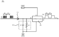
- 11A is a schematic structural diagram of an isolated power supply circuit provided by an embodiment of the present application.
- FIG. 11B is a schematic structural diagram of another isolated power supply circuit provided by an embodiment of the present application.
- FIG. 12 is a schematic structural diagram of another electronic device provided by an embodiment of the application.
- FIG. 13A is a schematic structural diagram of a first isolation element according to an embodiment of the present application.
- FIG. 13B is a schematic structural diagram of another first isolation element provided by an embodiment of the present application.
- FIG. 13C is a schematic structural diagram of another first isolation element provided by an embodiment of the present application.
- FIG. 14 is a schematic structural diagram of another electronic device provided by an embodiment of the application.
- 15A is a schematic cross-sectional structure diagram of an electronic device provided by an embodiment of the present application.
- 15B is a schematic diagram of a touch electrode, a first reference ground and a second reference ground provided by an embodiment of the present application;
- 15C is a schematic cross-sectional structure diagram of another electronic device provided by an embodiment of the present application.
- 16A is a schematic structural diagram of a touch control system provided by an embodiment of the present application.
- 16B is a schematic diagram of a touch control method of a touch control system provided by an embodiment of the present application.
- 17 is a schematic cross-sectional structure diagram of another electronic device provided by an embodiment of the present application.
- FIG. 18 is a schematic structural diagram of an isolated power supply circuit provided by an embodiment of the application.
- FIG. 19A is a schematic structural diagram of the signal conversion circuit shown in FIG. 18;
- FIG. 19B is a schematic structural diagram of the signal conversion circuit shown in FIG. 18;
- FIG. 19C is a schematic structural diagram of the signal conversion circuit shown in FIG. 18;
- 20 is a schematic structural diagram of another isolated power supply circuit provided by an embodiment of the present application.
- FIG. 21 is a schematic structural diagram of another electronic device provided by an embodiment of the application.
- FIG. 22 is a flowchart of a control method of an electronic device provided by an embodiment of the present application.
- first”, second, etc. are only used for descriptive purposes, and should not be understood as indicating or implying relative importance or implying the number of indicated technical features.
- a feature defined as “first”, “second”, etc. may expressly or implicitly include one or more of that feature.
- orientation terms such as “left”, “right”, “upper” and “lower” are defined relative to the orientation in which the components in the drawings are schematically placed, and it should be understood that these directional terms are Relative notions, they are used for relative description and clarification, which may vary accordingly depending on the orientation in which components are placed in the figures.
- electrical connection should be understood in a broad sense.
- electrical connection may be a direct electrical connection or an indirect electrical connection through an intermediate medium.
- Embodiments of the present application provide an electronic device.
- the electronic device may include a touch panel, a mobile phone, a tablet computer (pad), a TV, a smart wearable product (eg, a smart watch, a smart bracelet) and other electronic products with touch control functions.
- the embodiments of the present application do not specifically limit the specific form of the above electronic device.
- the electronic device 01 may include touch electrodes 10 , a cover plate 100 covering the touch electrodes 10 , and a touch electrode 10 electrically connected to the touch electrodes 10 as shown in FIG. 1 .
- the drive circuit 20 is detected.
- the touch detection driving circuit 20 is used for inputting touch excitation signals to the touch electrodes 10 and receiving detection signals from the touch electrodes 10 to realize touch detection.
- the cover plate 100 may be a substrate made of glass, polyethylene terephthalate (PET), or polycarbonate (PC).
- the cover plate 100 may be transparent (eg, the light transmittance may reach more than 85%), or may be completely opaque.
- the above-mentioned electronic device 01 may be a touch panel without a display function.
- the electronic device 01 may be provided with printed circuit boards (PCBs) as shown in FIG. 2A .
- the PCB can be stacked with the cover plate 100, and the cover plate 100 can be completely opaque. At this time, the metal layer in the PCB close to the cover plate 100 can be made into the above-mentioned touch electrodes 10 .
- the electronic device 01 when the above-mentioned electronic device 01 has a display function, the electronic device 01, as shown in FIG. 2B , may include a first display screen 02 and the above-mentioned cover plate 100, and the first display screen 01 is located on the first display screen.
- the above-mentioned first display screen 02 may be a liquid crystal first display screen (liquid crystal display, LCD), or may be an organic light emitting diode (organic light emitting diode, OLED) first display screen capable of realizing self-luminescence.
- the materials constituting the touch electrodes 10 may include transparent conductive materials, such as silver tin oxide (ITO) or indium zinc oxide (IZO).
- the electronic device 01 generally includes a plurality of the above-mentioned touch electrodes 10.
- the above-mentioned electronic device 01 may adopt a self-capacitive touch technology.
- the above-mentioned plurality of touch electrodes 10 may be a plurality of block-shaped self-capacitance electrodes 11 as shown in FIG. 3 .
- the plurality of self-capacitance electrodes 11 may be spaced along the first direction Y at a predetermined interval distance h1.
- the above-mentioned plurality of self-capacitance electrodes 11 may also be arranged along the second direction X at a predetermined interval distance h2.
- the plurality of self-capacitance electrodes 11 can be formed of the same conductive layer, and since the plurality of self-capacitance electrodes 11 are not connected to each other, the plurality of self-capacitance electrodes 11 can be insulated.
- the first direction X and the second direction Y may be arranged to intersect.
- the touch detection driving circuit 20 may include a driving detection terminal 201 , and each self-capacitance electrode 11 may be electrically connected to the driving detection terminal 201 of the touch detection driving circuit 20 through a touch wire 12 . .
- the touch detection driving circuit 20 may include an excitation generating unit 210 and a capacitance detection unit 221 as shown in FIG. 4A .
- the excitation generating unit 210 can send the touch excitation signal S1 to the self-capacitance electrode 11 in the sampling period T through the above-mentioned driving and detecting terminal 201 .
- the touch excitation signal S1 may be a square wave signal.
- the touch excitation signal S1 may be a square wave signal with a sampling frequency of 120 Hz (ie, 120 samples per second), and a scanning frequency greater than 100 KHz (eg, 300 KHz) in each sampling period T.
- the above-mentioned touch excitation signal S1 may include a touch phase P1 and a non-touch phase P2.
- the touch phase P1 the area with denser square waves in FIG. 5
- the touch excitation signal S1 can scan all the self-capacitance electrodes 11 in the electronic device 01 at least once at a scan frequency greater than 100KHz (eg, 300KHz).
- the non-touch phase P1 the touch excitation signal S1 is always at a low level.
- the peak-to-peak value of the excitation signal S1 may be 3.3V.
- a small parasitic capacitance Cm exists between the self-capacitance electrode 11 and the reference ground (eg, GND).
- the capacitance detection unit 221 in the touch detection driving circuit 20 detects the charging and discharging time of the parasitic capacitance Cm in each touch stage P1 through the driving detection terminal 201.
- the charging and discharging time of the parasitic capacitance Cm is constant.
- the touch detection driving circuit 20 provides the touch excitation signal S1 with a peak-to-peak value of 3.3V to the self-capacitance electrode 11 , the voltage difference between the positive and negative electrode plates of the parasitic capacitor Cm is about 3.3V.
- the finger When the finger is close to the self-capacitance electrode 11 , as shown in FIG. 4B , the finger can be equivalent to the reference ground (eg, 0V), and an equivalent capacitance Cp is formed between the finger and the self-capacitance electrode 11 .
- the touch detection driving circuit 20 provides the touch excitation signal S1 with a peak-to-peak value of 3.3V to the self-capacitance electrode 11 , the voltage difference between the positive and negative electrode plates of the equivalent capacitor Cp is about 3.3V.
- the touch detection driving circuit 20 needs to detect the charging and discharging time of the parasitic capacitance Cm and the equivalent capacitance Cp at the same time, so that the charging and discharging time of the capacitance detected by the touch detection driving circuit 20 will be greatly increased. extend.
- the touch detection driving circuit 20 can calculate the size of the equivalent capacitance Cp through the detected actual charging and discharging time and the charging and discharging time of the parasitic capacitance Cm as a constant, so as to achieve the purpose of touch detection.
- the above-mentioned electronic device 01 may adopt the mutual capacitive touch technology.
- the above-mentioned plurality of touch electrodes 10 may include a plurality of transmission electrodes TX and a plurality of reception electrodes RX as shown in FIG. 6A , and the plurality of transmission electrodes TX and the plurality of reception electrodes RX are intersected and insulated.
- each of the plurality of transmission electrodes TX may extend along the first direction Y, and the plurality of transmission electrodes TX may be arranged side by side along the second direction X at a predetermined interval distance h3.
- Each receiving electrode RX in the above-mentioned plurality of receiving electrodes RX may extend along the second direction X, and the plurality of receiving electrodes RX may be arranged side by side along the first direction Y at a certain preset interval distance h4, so that a plurality of transmitting electrodes RX can be arranged side by side.
- the electrode TX and a plurality of receiving electrodes RX are arranged to intersect.
- the above-mentioned transmitting electrode TX and receiving electrode RX can be formed by using two different conductive layers, and the two conductive layers are insulated by an insulating layer.
- the touch detection driving circuit 20 may include a driving terminal 202 and a detection terminal 203 .
- Each transmission electrode TX may be electrically connected to the driving terminal 202 .
- Each receiving electrode RX is electrically connected to the detection terminal 203 .
- any one of the transmitting electrode TX and the receiving electrode RX may include a plurality of block electrodes 110 and a strip electrode 112 connected to the plurality of block electrodes 110 .
- a parasitic capacitance Cm can be formed between the block electrodes 110 of a transmitting electrode TX and the block electrodes 110 of a receiving electrode RX, so that, for example, Any group of the transmitting electrodes TX and receiving electrodes RX that are crossed horizontally and vertically as shown in FIG. 6A has the above-mentioned parasitic capacitance Cm at the crossing position.
- the touch detection driving circuit 20 can send the above-mentioned touch excitation signal S1 (as shown in FIG. 5 ) to the transmitting electrode TX through the driving terminal 202 shown in FIG. 6A , so as to prevent the parasitic The capacitor Cm is charged.
- the touch detection driving circuit 20 will also detect the detection signal of the receiving electrode RX through the detection terminal 203 to determine the discharge of the parasitic capacitance Cm in each touch stage P1. time, and get the capacitance value of Cm.
- the above-mentioned parasitic capacitance Cm is constant.
- the finger can be equivalent to the reference ground (for example, 0V), and an equivalent capacitance Cp is formed between the finger and the transmitting electrode TX. Therefore, as shown in FIG. 6C , it is equivalent to connecting an equivalent capacitance Cp in parallel with both ends of the parasitic capacitance Cm. In this way, when the touch detection driving circuit 20 detects that the capacitance value increases, it can be determined that there is a finger touch, so as to achieve the purpose of touch detection.
- the closer the finger is to the touch electrode the larger the capacitance value of the equivalent capacitance Cp is, and the farther away the touch electrode is, the smaller the capacitance value of the equivalent capacitance Cp is. Therefore, when the finger is far away from the touch electrode for floating touch, it will lead to The touch detection accuracy is further reduced.
- the embodiment of the present application can improve the signal detection resolution and signal-to-noise ratio of the equivalent capacitance Cp, so that the finger, as shown in FIG. , H ⁇ 20mm), the accurate detection of the charge and discharge time of the equivalent capacitance Cp can also be achieved, so as to achieve the purpose of floating touch.
- the electronic device provided in this embodiment of the present application may include a first reference ground as shown in FIG. 8 .
- GND1 for example, 0V
- the second reference ground GND2 for example, the peak-to-peak voltage may be about 20V
- the above-mentioned parasitic capacitance Cm is formed between the touch electrode 10 and the second reference ground GND2.
- the touch electrode 10 and the second reference ground GND2 (20V) can be used as the positive and negative electrode plates of the parasitic capacitance Cm, respectively.
- the excitation signal S1 is controlled, the voltage of the touch electrodes 10 is 23.3V, and the voltage difference between the positive and negative electrode plates of the parasitic capacitor Cm is about 3.3V.
- the finger when the finger is close to the touch electrode 10 , the finger can be equivalent to the first reference ground GND1 (eg, 0V), and an equivalent capacitance Cp is formed between the finger and the touch electrode 10 .
- the touch electrode 10 and the finger equivalent to the first reference ground GND1 can be used as the positive and negative electrode plates of the equivalent capacitance Cp, respectively.
- the voltage of the touch electrode 10 is 23.3V
- the voltage difference between the positive and negative electrode plates of the equivalent capacitance Cp can be about 23.3V.
- the voltage difference between the positive and negative electrode plates of the equivalent capacitor Cp can be increased from the original 3.3V to 23.3V , so that the electrical signal used for detecting the charging and discharging time of the equivalent capacitance Cp is amplified, so as to achieve the purpose of increasing the resolution of the signal detection of the equivalent capacitance Cp.
- the voltage difference between the positive and negative electrode plates of the equivalent capacitance Cp is relatively large (for example, 23.3V)
- the voltage difference between the positive and negative electrode plates of the parasitic capacitance Cm is small (for example, about 3.3V). Therefore, although the detection of the charging and discharging process of the parasitic capacitance Cm by the touch detection driving circuit 20 will be regarded as noise, the proportion between the noise and the detection signal obtained by detecting the charging and discharging process of the equivalent capacitance Cp is relatively small. Therefore, the purpose of improving the signal-to-noise ratio of touch detection can be achieved.
- the detection range suitable for hovering touch can be increased from 5 mm to more than 20 mm, and some It is beneficial to improve the comfort of the user's hovering touch.
- the present application adopts to raise the voltage of the second reference ground GND2, the purpose of increasing the detection range suitable for floating touch and improving the touch detection accuracy is achieved.
- the semiconductor device in the electronic device 01 does not need to adopt a high-voltage and high-speed process, which is beneficial to reduce production costs.
- the voltage of the touch excitation signal S1 is too high (for example, 10V), which causes the touch electrode 10 to break down.
- the touch-control scheme using ultrasonic waves, time of flight (TOF) or invisible light, etc. as the transmission signal the finger needs to be in a specific area to receive the above-mentioned transmission signal.
- the capacitive touch is used to realize the floating touch, and the coverage of the touch electrodes 10 can be adjusted as required, which is beneficial to increase the user's range of motion during the floating touch.
- the touch electrode 10 as the self-capacitance electrode as an example.
- the receiving electrode RX and the receiving electrode RX can be similarly
- the first reference ground GND1 for example, 0V
- the second reference ground GND2 for example, the voltage peak-to-peak value can be about 20V
- the parasitic capacitance Cm formed between the transmitting electrode TX and the receiving electrode RX The voltage difference between the positive and negative electrode plates is about 3.3V.
- the voltage of the negative electrode plate of the parasitic capacitance Cm needs to be raised from the original first reference ground GND1 (for example, 0V) to the second reference ground GND2 (For example, the peak-to-peak voltage may be around 20V).
- the touch detection driving circuit 20 can provide the touch excitation signal S1 to the touch electrode 10 serving as the positive electrode plate of the parasitic capacitance Cm.
- the touch detection drive circuit 20 needs to be disconnected (ie isolated) from the first reference ground GND1 (for example, 0V) and electrically connected to the second reference ground GND2 (for example, the voltage peak-to-peak value can be about 20V), in order to be able to output normally The above touch excitation signal S1.
- the following takes the touch electrode 10 as a self-capacitance electrode as an example to illustrate the setting method of the second reference ground GND2 and the power supply method of the touch detection driving circuit 20 in detail.
- the above electronic device 01 further includes an isolated power supply circuit 30 and an AC amplifier circuit 40 as shown in FIG. 9A .
- the isolated power supply circuit 30 is electrically connected to the touch detection driving circuit 20 and the above-mentioned first reference ground GND1 and second reference ground GND2.
- the isolated power supply circuit 30 can be used to receive the touch excitation signal S1, and according to the touch excitation signal S1 in the non-touch detection stage P2 (as shown in FIG. 5), the first reference ground GND1 and the second reference ground GND2 are short-circuited , the primary supply voltage Vin is stored.
- the isolated power supply circuit 30 is also used for transmitting the primary power supply voltage Vin to the touch detection driving circuit 20 to supply power to the touch detection driving circuit 20 .
- the touch drive detection circuit 20 can be grounded through the second reference ground GND2. Since the first reference ground GND1 and the second reference ground GND2 are short-circuited, the voltage of the second reference ground GND2 is now the same as the first reference ground GND1. the same voltage, such as 0V. Therefore, when the isolated power supply circuit 30 transmits the primary power supply voltage Vin to the touch detection driving circuit 20, the touch driving detection circuit 20 can be in a working state and output the touch excitation signal S1.
- the isolation power supply circuit 30 may disconnect the first reference ground GND1 and the second reference ground GND2 to isolate the first reference ground GND1 and the second reference ground GND2 .
- the isolated power supply circuit 30 can release the electrical energy stored in the non-touch detection stage P2 to the touch detection driving circuit 20 to supply power to the touch detection driving circuit 20 .
- the touch driving detection circuit 20 can be grounded through the second reference ground GND2, and the peak-to-peak value of the voltage on the second reference ground GND2 can be about 20V. Therefore, when the isolated power supply circuit 30 discharges to the touch detection driving circuit 20 , the touch driving detection circuit 20 can still maintain the working state and output the touch excitation signal S1 .
- the isolated power supply circuit 30 can short-circuit the first reference ground GND1 and the second reference ground GND2, so that the power supply for providing the primary power supply voltage Vin It is electrically connected with the touch driving detection circuit 20 to drive the touch driving detection circuit 20 to output the touch excitation signal S1.
- the isolated power supply circuit 30 can disconnect the first reference ground GND1 from the second reference ground GND2 , so that the power supply for providing the primary power supply voltage Vin and the touch drive detection circuit 20 is isolated, and the stored power is discharged to the touch drive detection circuit 20 to drive the touch drive detection circuit 20 to output the touch excitation signal S1. In this way, after the power is turned on, the isolated power supply circuit 30 can keep the touch drive detection circuit 20 in a working state.
- the above-mentioned AC amplifier circuit 40 can use the first reference ground GND1 and the second reference ground GND2 is electrically connected.
- the AC amplifying circuit 40 is grounded through the first reference ground GND1, and can be used to receive and amplify the touch excitation signal S1 during operation to generate a voltage adjustment signal S2 as shown in FIG. 9B, and convert the voltage adjustment signal to the S2 is transmitted to the second reference ground GND2 as shown in FIG. 9A .
- the peak-to-peak value (eg, about 20V) of the voltage adjustment signal S2 may be greater than the voltage value (eg, 0V) of the first reference ground.
- the AC amplifying circuit 40 will not change the period of the touch excitation signal S1, so the low frequency part of the generated voltage adjustment signal S2, as shown in FIG. 9B, still has the above sampling period T ( Including touch stage P1 and non-touch stage P2).
- the center bias voltage (for example, 10V) of the voltage adjustment signal S2 can be set according to a preset amplification factor, and then the valley voltage of the voltage adjustment signal S2 can be set ( For example, 0V) and a peak-to-peak voltage (for example, 20V), so that the peak-to-peak value (for example, about 20V) of the voltage adjustment signal S2 meets the requirement of the preset amplification factor.
- the AC amplifier circuit 40 can make the maximum voltage on the second reference ground GND2 be about 20V.
- the touch detection driving circuit 20 is isolated from the power supply for providing the primary power supply voltage Vin, and is grounded through the second reference ground GND2. When the isolated power supply circuit 30 supplies power to the touch detection driving circuit 20 , the touch detection driving circuit 20 can maintain a working state, thereby outputting the touch excitation signal S1 .
- the touch detection driving circuit 20 provides the touch excitation signal S1 to the touch electrodes 10 , and as shown in FIG. 5 , the peak-to-peak value of the signal S1 may be 3.3V.
- the AC amplifying circuit 40 amplifies the touch excitation signal S1 to generate a voltage adjustment signal S2 , as shown in FIG. 9B , the peak-to-peak value of which can be 20V.
- the voltage difference between the touch electrodes 10 and the second reference ground GND2 remains unchanged (ie, the capacitance value of the parasitic capacitance Cm remains unchanged), so the maximum value of the voltage on the touch electrodes 10 is 23.3V.
- the above-mentioned equivalent capacitance Cp is formed between the finger equivalent to the first reference ground GND1 (eg, 0V) and the touch electrode 10 .
- the voltage difference between the two electrode plates (the finger and the touch electrode 10 ) of the equivalent capacitance Cp may be 23.3V. Therefore, the electrical signal used for detecting the charging and discharging time of the equivalent capacitance Cp is amplified, and the purpose of increasing the resolution of the signal detection of the equivalent capacitance Cp is achieved.
- the voltage difference between the two electrode plates (the touch electrode 10 and the second reference ground GND2 ) of the parasitic capacitance Cm is 3.3V.
- the ratio of the noise generated by the parasitic capacitance Cm to the detection signal obtained by detecting the charging and discharging process of the equivalent capacitance Cp is small, so that the purpose of improving the signal-to-noise ratio of touch detection can be achieved, which is conducive to the realization of suspension touch.
- the peak-to-peak value of the touch excitation signal S1 output by the touch detection drive circuit 20 is 3.3V
- the peak-to-peak value of the voltage adjustment signal S2 output by the AC amplifier circuit 40 to the second reference ground GND2 is 23.3V Explanation as an example.
- the present application does not limit the peak-to-peak value of the touch excitation signal S1 and the amplification factor n of the AC amplifying circuit 40 .
- the peak-to-peak value of the touch excitation signal S1 may be less than or equal to 5V
- the amplification factor n of the AC amplifier circuit 40 may be greater than or equal to 2, so that the peak-to-peak value of the voltage adjustment signal S2 output by the AC amplifier circuit 40 is greater than or equal to 10V.
- the power supply may include a battery 60 and a first power management unit (power management unit, PMU) 61 .
- the first PMU 61 is electrically connected to the battery 60 , the isolated power supply circuit 30 and the above-mentioned AC amplifier circuit 40 .
- the first PMU 61 can convert the battery voltage Vbat of the battery 60 into the above-mentioned primary power supply voltage Vin and transmit it to the isolated power supply circuit 30 .
- the first PMU 61 can also convert the battery voltage Vbat of the battery 60 into the working voltage V1 of the AC amplifier circuit 40 to supply power to the AC amplifier circuit 40 .
- the AC amplifying circuit 40 may include an operational amplifier 401 as shown in FIG. 11A , a first capacitor C1 , a second capacitor C2 , a first resistor R1 , and a second resistor R2 .
- the first end of the first capacitor C1 is electrically connected to the touch detection driving circuit 20 as shown in FIG. 10 to receive the touch excitation signal S1 output by the touch detection driving circuit 20 .
- the second terminal of the first capacitor C1 is electrically connected to the positive input terminal (“+”) of the operational amplifier 401 .
- the first terminal of the first resistor R1 is electrically connected to the negative input terminal (“-”) of the operational amplifier 401
- the second terminal of the first resistor R1 is electrically connected to the first terminal of the second capacitor C2
- the second end of the second capacitor C2 is electrically connected to the first reference ground GND1.
- the first terminal of the second resistor R2 is electrically connected to the negative input terminal (“-”) of the operational amplifier 401
- the second terminal of the second resistor R2 is electrically connected to the output terminal of the operational amplifier 401 .
- the output terminal of the operational amplifier 401 is electrically connected to the second reference ground GND2, and the control terminal of the operational amplifier 401 is electrically connected to the control voltage terminal VCC.
- the touch excitation signal S1 which is an AC signal
- the touch excitation signal S1 can be transmitted to the positive input terminal (“+”) of the operational amplifier 401 through the first capacitor C1 .
- the first resistor R1, the second resistor R2, and the second capacitor C2 may constitute an AC amplifying unit, and the AC amplifying unit can amplify the peak-to-peak voltage (eg, 3.3V) of the touch excitation signal S1 to R2/R1 times, so that the The peak-to-peak value of the output terminal voltage of the operational amplifier 401 may be close to the full scale of the operational amplifier 401 (ie, the voltage value of the control voltage terminal VCC, eg, 20V). In this way, the voltage of the second reference ground GND2 can be raised to 20V.
- the above-mentioned AC amplifier circuit 40 may also have a voltage bias function.
- the AC amplifier circuit 40 may further include a third resistor R3 and a fourth resistor R4 .
- the first terminal of the third resistor R3 is electrically connected to the control voltage terminal VCC, and the second terminal of the third resistor R3 is electrically connected to the positive input terminal (“+”) of the operational amplifier 401 .
- the first terminal of the fourth resistor R4 is electrically connected to the positive input terminal (“+”) of the operational amplifier 401
- the second terminal of the fourth resistor R4 is electrically connected to the first reference ground GND1 .
- the resistance values of the third resistor R3 and the fourth resistor R4 are the same.
- the center bias voltage Va can be generated at the center bias point a.
- the central bias voltage Va may be 10V.
- the peak-to-peak value of the output terminal voltage of the operational amplifier 401 can be close to the full operational amplifier of the operational amplifier 401.
- Range that is, the voltage value of the control voltage terminal VCC, such as 20V.
- the voltage of the second reference ground GND2 can be raised to 20V.
- the center bias voltage Va is generated at the center bias point a, which can make the operational amplification process of the operational amplifier 401 more stable.
- the AC amplifier circuit 40 in order to make the AC amplifier circuit 40 work normally, in addition to the need for the battery 60 to supply power to the AC amplifier circuit 40 through the first PMU 61, the AC amplifier circuit 40 also needs to be electrically connected to the first reference ground GND1 to provide power to the AC amplifier circuit 40. achieve grounding. It can be seen from the above that the touch detection driving circuit 20 is electrically connected to the second reference ground GND2 to realize grounding, and the touch excitation signal S1 output by the touch detection driving circuit 20 needs to be transmitted to the AC amplifier circuit 40 .
- the above-mentioned electronic device 01 may further include a first isolation element 51 .
- the first isolation element 51 is coupled between the touch detection driving circuit 20 and the AC amplifier circuit 40 , and between the touch detection driving circuit 20 and the isolation power circuit 30 .
- the first isolation element 51 is also electrically connected to the first reference ground GND1 and the second reference ground GND2, and is used for coupling the touch excitation signal S1 output by the touch detection drive circuit 20 to the AC amplifier circuit 40 and the isolated power supply circuit 30 .
- the aforementioned electronic device 01 may further include a processor 70 .
- the processor 70 may be a central processing unit (central processing unit, CPU), or a system on a chip (system on a chip, SOC).
- the above-mentioned first PMU 61 can convert the battery voltage Vbat of the battery 60 into the working voltage V2 of the processor 70 .
- the processor 70 may receive the detection result of the touch detection driving circuit 20, and determine the position of the finger touch, the type of the gesture, and the like according to the detection result.
- the processor 70 can also output a control signal to the touch detection driving circuit 20 to control the touch detection process of the touch detection driving circuit 20 .
- the processor 70 needs to be electrically connected to the first reference ground GND1 to achieve grounding. It can be seen from the above that the touch detection driving circuit 20 is electrically connected to the second reference ground GND2 to realize grounding.
- the above-mentioned electronic device 01 may further include a second isolation element 52 .
- the second isolation element 52 is coupled between the processor 70 and the touch detection driving circuit 20 .
- the second isolation element 52 is electrically connected to the first reference ground GND1 and the second reference ground GND2, and is used for coupling the control signal output by the processor 70 to the touch detection driving circuit 20, and for obtaining the touch detection driving circuit 20 The result of the touch detection is coupled to the processor 70 .
- the structure of the first isolation element 51 may be as shown in FIG. 13A , including a light emitting device 501 and a photoelectric converter 502 .
- the light emitting device 501 can be electrically connected to the touch detection driving circuit 20 for converting the touch excitation signal S1 from the touch detection driving circuit 20 into an optical signal.
- the photoelectric converter 502 can be electrically connected to the AC amplifying circuit 40 and the isolated power supply circuit 30 for converting the optical signal into an electrical signal and transmitting it to the AC amplifying circuit 40 and the isolated power supply circuit 30 .
- the above-mentioned first isolation element 51 adopts an optocoupler method to couple and transmit signals.
- the above-mentioned light-emitting device 501 may be a light-emitting diode or a laser transmitter.
- the structure of the first isolation element 51 may be as shown in FIG. 13B , including: a signal input interface 503 , an isolation capacitor 504 and a signal output interface 505 .
- the signal input interface 503 is electrically connected to the touch detection driving circuit 20 for receiving the touch excitation signal S1 from the touch detection driving circuit 20 .
- the first end of the isolation capacitor 504 is electrically connected to the signal input interface 503
- the second end of the isolation capacitor 504 is electrically connected to the signal output interface 505 .
- the isolation capacitor 504 is used to transmit the touch excitation signal S1 received by the signal input interface 503 to the AC amplifier circuit 40 and the isolation power supply circuit 30 through the signal output interface 505 .
- the above-mentioned first isolation element 51 uses capacitive coupling to perform signal coupling and transmission.
- the structure of the first isolation element 51 may be as shown in FIG. 13C , including a sound generating device 506 and an acoustic-electric converter 507 .
- the sound generating device 506 is electrically connected to the touch detection driving circuit 20 for converting the touch excitation signal S1 from the touch detection driving circuit 20 into a sound signal.
- the acoustic-electrical converter 507 is electrically connected to the AC amplifying circuit 40 and the isolated power supply circuit 30 for converting the sound signal into an electrical signal and transmitting it to the AC amplifying circuit 40 and the isolated power supply circuit 30 .
- the above-mentioned first isolation element 51 adopts an acoustic coupling method to couple and transmit signals.
- the first isolation element 51 may further include a transformer, the primary winding of the transformer is electrically connected to the touch detection drive circuit 20 , and the secondary winding is electrically connected to the AC amplifier circuit 40 , Thereby, the coupling transmission of the signal is carried out by means of the electromagnetic coupling of the transformer.
- the above description takes the structure of the first isolation element 51 as an example, and the structure of the second isolation element 62 can be obtained in the same way, and will not be repeated here.
- the above electronic device 01 may also include The first circuit board 101 and the second circuit board 102 .
- the first circuit board 101 and the second circuit board 102 may both be PCB boards.
- the PCB board may include multiple layers of copper foils and a dielectric layer disposed between any two adjacent layers of copper foils.
- the second reference ground GND2 can be set in the first circuit board 101 .
- a layer of copper foil in the first circuit board 101 can be used as the reference ground plane where the second reference ground GND2 is located.
- the touch detection driving circuit 20 can be disposed on the first circuit board 101 , so that the touch detection driving circuit 20 can be electrically connected to the second reference ground GND2 for grounding.
- the above-mentioned first reference ground GND1 may be provided in the second circuit board 102 .
- a layer of copper foil in the second circuit board 102 can be used as the reference ground plane where the first reference ground GND1 is located.
- other control circuits in the electronic device 01 such as the above-mentioned processor 70 , the isolated power supply circuit 30 , the AC amplifier circuit 40 , the first isolation element 51 , the second isolation element 52 and the The first PMU 61 is disposed on the second circuit board 102 , so that the above-mentioned other control circuits can be electrically connected to the first reference ground GND1 to realize grounding.
- the isolation power circuit 30 , the first isolation element 51 and the second isolation element 52 are all electrically connected to the first reference ground GND1 and the second reference ground GND2 . Therefore, in some embodiments of the present application, as shown in FIG. 14 , the isolated power supply circuit 30 , the first isolation element 51 and the second isolation element 52 may be arranged on the second circuit board 102 , so that the isolated power supply circuit 30 , The first isolation element 51 and the second isolation element 52 are directly and electrically connected to the first reference ground GND1 in the second circuit board 102 , and are electrically connected to the second reference ground GND2 in the first circuit board 101 through traces.
- the isolated power circuit 30 , the first isolation element 51 and the second isolation element 52 may be disposed on the first circuit board 101 , so that the isolated power circuit 30 , the first isolation element 51 And the second isolation element 52 is directly electrically connected to the second reference ground GND2 in the first circuit board 101 , and is electrically connected to the first reference ground GND2 in the second circuit board 102 through traces.
- the description is given by taking the isolation power supply circuit 30 , the first isolation element 51 and the second isolation element 52 disposed on the second circuit board 102 as an example.
- the processor 70 and the touch detection driving circuit 20 may be disposed on the first circuit board 101 .
- both the processor 70 and the touch detection driving circuit 20 may be electrically connected through the second reference ground GND2 in the first circuit board 101 to realize grounding.
- the processor 70 and the touch detection driving circuit 20 are electrically connected to the same reference ground, that is, the second reference ground GND2. Therefore, the above-mentioned second isolation element 52 does not need to be disposed between the processor 70 and the touch detection driving circuit 20 .
- other circuit structures electrically connected to the processor 70 such as a Bluetooth circuit, may also be disposed in the above-mentioned first circuit board 101 together with the processor 70 .
- the above-mentioned first circuit board 101 and second circuit board 102 may be stacked and disposed, wherein the first circuit board 101 is closer to the second circuit board 102 than the second circuit board 102
- the cover plate 100 is provided.
- the first circuit board 101 includes a multi-layer copper foil, wherein a layer of copper foil closest to the cover plate 100 among the above-mentioned multi-layer copper foils 101 can be referred to as the first copper foil 111 .
- the first copper foil 111 may include a plurality of spaced and block-shaped first copper foils 111 .
- the above-mentioned touch electrodes 10 can be fabricated by using a layer of copper foil in the first circuit board 101 .
- the touch electrodes 10 may be connected to the cover plate 100 through an adhesive layer.
- a layer of copper foil in the first circuit board 101 can be used as the reference ground plane where the second reference ground GND2 is located, and a layer of copper foil in the second circuit board 102 can be used as the reference where the first reference ground GND1 is located. horizon.
- the second reference ground GND2 may be stacked with the first reference ground GND1 .
- the vertical projections of the plurality of touch electrodes 10 formed by the first copper foil 111 in the first circuit board on the second reference ground GND2 are all located in the plane where the second reference ground GND2 is located. .
- the first circuit board 101 may include a laminated and insulated
- the first copper foil 111 and the second copper foil 222 have an insulating layer between the first copper foil 111 and the second copper foil 222 .
- the first copper foil 111 may include the above-mentioned plurality of transmitting electrodes TX.
- the second copper foil 222 may include the above-described plurality of receiving electrodes RX.
- the cover plate 100 may be connected to the above-mentioned plurality of transmitting electrodes TX through an adhesive layer.
- the first copper foil 111 is the copper foil closest to the cover plate 100 in the first circuit board 101 .
- the cover plate 100 may be connected to the above-mentioned plurality of receiving electrodes RX through an adhesive layer.
- the second copper foil 222 is the copper foil closest to the cover plate 100 in the first circuit board 101 .
- the above-mentioned touch detection driving circuit 20 may be disposed on a surface of the first circuit board 101 away from the cover plate 100 .
- other control circuits in the electronic device 01 such as the above-mentioned processor 70, the isolated power supply circuit 30, the AC amplifier circuit 40, etc., can be arranged on the side surface of the second circuit board 102 close to the first circuit board 101, or can be arranged on the surface of the second circuit board 102. on the side surface of the second circuit board 102 away from the first circuit board 101 .
- control circuits on the second circuit board 101 can be connected to the first circuit board 101 through inter-board connectors or cables.
- the touch detection driving circuit 20 is electrically connected.
- the battery 60 disposed on the side of the second circuit board 102 away from the first circuit board 101 can supply power to the above-mentioned control circuit.
- the touch detection driving circuit 20 and other control circuits in the electronic device (such as the above-mentioned processor 70, the isolated power supply circuit 30, the AC amplifier circuit can be made) 40, etc.) on different circuit boards.
- the failure of the other control circuits mentioned above during the attaching process can be reduced, and it is beneficial to the first circuit board 101.
- the touch detection drive circuit 20 on the device is tested.
- the touch electrodes 10 in the electronic device 01 usually have a relatively large number, such as 400, the number of signal lines used to electrically connect the touch electrodes 10 and the touch detection driving circuit 20 together is also relatively large. Therefore, it is necessary to set the touch detection driving circuit 20 and the touch electrodes 10 on the same circuit board, which is beneficial to the connection of the above-mentioned signal lines.
- the touch control system includes an electronic device 01 as a touch panel and a display terminal 03 as shown in FIG. 16A .
- the electronic device may further include a first transmission element 81, and the first transmission element 81 may be electrically connected with the second transmission element 82 of the display terminal 03 in a wired or wireless manner (as shown in FIG. 16B ).
- the processor 70 in the electronic device can calculate the touch coordinate data of the user's finger according to the detection result of the touch detection driving circuit 20 and transmit it to the second transmission element 82 through the first transmission element 81 .
- the display end processor 83 parses the touch coordinate data, and controls the second display screen 04 in the display terminal 03 to display the cursor 90 as shown in FIG. 16B .
- the display-side PMU in FIG. 16A is used to supply power to the second display screen 04, the display-side processor 83 and the memory.
- the memory is used to store the information output by the display side processor 83 .
- the touch electrodes 10 may be disposed on the first display screen 02 and the cover plate between 100.
- the touch electrodes 10 may include the above-mentioned self-capacitance electrodes.
- the touch electrode 10 may include a stacking transmitting electrode TX and a receiving electrode RX.
- the electronic device 01 may include a first circuit board 101 and a second circuit board 102 which are arranged in layers.
- the second reference ground GND2 is disposed in the first circuit board 101
- the touch detection driving circuit 20 may be disposed on a surface of the first circuit board 101 away from the cover plate 100 .
- the first reference ground GND1 may be disposed in the second circuit board 102 .
- Other control circuits in the electronic device 01 such as the above-mentioned processor 70 , the isolated power supply circuit 30 , the AC amplifier circuit 40 , the first isolation element 51 , the second isolation element 52 and the first PMU 61 are disposed on the second circuit board 102 .
- the above-mentioned electronic device 01 may be a mobile phone, a smart wearable product or a tablet computer.
- the isolation power supply circuit 30 can short-circuit the first reference ground GND1 and the second reference ground GND2, and transmit the primary power supply voltage Vin provided to the first PMU 61 to the touch detection driving circuit 20,
- the above-mentioned touch excitation signal S1 is output by driving the touch detection driving circuit 20 to work.
- the primary power supply voltage Vin is stored to realize the energy storage process.
- the isolation power supply circuit 30 can disconnect the first reference ground GND1 and the second reference ground GND2, and discharge the touch detection driving circuit 20, so as to drive the touch detection driving circuit 20 to work to output the above-mentioned touch detection and driving circuit 20. Control excitation signal S1.
- the specific structure of the isolated power supply circuit 30 capable of realizing the above functions will be described in detail below.
- the isolated power supply circuit 30 may include a signal conversion circuit 301 , a first tank circuit 302 , a first switch circuit 303 and a second switch circuit 304 .
- the above-mentioned signal conversion circuit 301 is used to receive the touch excitation signal S1, and filter out the high frequency part in the touch excitation signal S1 (in the area where the square waves are denser in FIG. 18, the frequency can be greater than 100KHz) to generate the sampling signal S3.
- the low-frequency part of the sampling signal S3 still has the above-mentioned sampling period T (including the touch phase P1 and the non-touch phase P2).
- FIG. 18 illustrates an example in which the low-frequency part of the touch excitation signal S1 and the sampling signal S3 are at a high level in the touch phase P1 and are at a low level in the non-touch phase P2 .
- the structure of the signal conversion circuit 301 may be as shown in FIG. 19A , including a diode 311 , a second tank circuit 321 , a third switch circuit 331 and an inverter 341 .
- the input end of the diode 311 is used for receiving the above-mentioned touch excitation signal S1.
- the first isolation element 51 is coupled between the touch detection driving circuit 20 and the isolation power supply circuit 30.
- the isolation power supply circuit 30 can be connected to the input terminal of the diode 311 in the signal conversion circuit 301 through the input terminal of the diode 311 as shown in the figure.
- the first isolation element 51 shown at 12 is electrically connected. In this way, the input end of the diode 311 can receive the touch excitation signal S1 through the first isolation element 51 .
- the second tank circuit 321 may be electrically connected to the output terminal of the diode 311 and the first reference ground GND1. Exemplarily, as shown in FIG. 19A , the second tank circuit 321 may include a capacitor C and an inductor L1 .
- the control terminal g3 of the third switch circuit 331 may be electrically connected to the output terminal of the diode 311 and the second tank circuit 321 .
- the first end a3 of the third switch circuit 331 may be electrically connected to the first reference ground GND1.
- the second terminal b3 of the third switch circuit 331 may be electrically connected to the control terminal g1 of the first switch circuit 303 and the control terminal g2 of the second switch circuit 304 (as shown in FIG. 18 ).
- the third switch circuit 311 is used for disconnecting the control terminal g1 of the first switch circuit 303 and the control terminal g2 of the second switch circuit 304 from the first reference ground GND1 in the non-touch detection stage P2 in an off state.
- the voltage of the first voltage terminal VDD1 is transmitted to the control terminal g1 of the first switch circuit 303 and the control terminal g2 of the second switch circuit 304 .
- the control terminal g1 of the first switch circuit 303 and the control terminal g2 of the second switch circuit 304 are short-circuited with the first reference ground GND1.
- the inverter 341 may be electrically connected between the second terminal b3 of the third switch circuit 331 and the control terminal g1 (as shown in FIG. 18 ) of the first switch circuit 303 , and may be electrically connected to the third switch circuit 331 . Between the second terminal b3 and the control terminal g2 of the second switch circuit 304 (as shown in FIG. 18 ).
- the signal conversion process of the signal conversion circuit 301 is illustrated by taking the above-mentioned third switch circuit 331 as an N-channel metal oxide semiconductor transistor (negative channel metal oxide semiconductor, NMOS) as an example.
- NMOS negative channel metal oxide semiconductor
- the touch detection stage P1 when the touch excitation signal S1 is at a high level as shown in FIG. 19A, the high level is transmitted to the control terminal of the above-mentioned NMOS transistor (ie, the third switch circuit 331) through the diode 311 to control the NMOS The transistor is turned on, thereby short-circuiting the first voltage terminal VDD1 with the first reference ground GND1. At the same time, the capacitor C and the inductor L1 in the second energy storage circuit 321 can store the high level.
- the input terminal of the inverter 341 receives the low level of the first reference ground GND1, and reverses the low level before outputting, so the inverter 341 outputs a high level at this time, that is, sampling The signal S3 is at a high level at this time.
- the second energy storage circuit 321 can keep the NMOS transistor in an on state. Since the frequency of the touch excitation signal S1 is very fast (for example, about 300KHz) in the touch detection stage P1, before the discharge of the second energy storage circuit 321 ends, the touch excitation signal S1 is quickly switched from a low level to a low level. to a high level, so that the NMOS transistor continues to be in a conducting state. In this way, the sampling signal S3 maintains a high level during the entire touch detection stage P1.
- the non-touch detection stage P2 when the touch excitation signal S1 is at a low level, the low level is transmitted to the control terminal of the NMOS transistor (ie, the third switch circuit 331) through the diode 311 to control the NMOS transistor to be turned off.
- the high level output from the first voltage terminal VDD1 is transmitted to the input terminal of the inverter 341 after the freewheeling action of the inductor L2, and the inverter 341 reverses the high level before processing the high level. Therefore, the inverter 341 outputs a low level at this time, that is, the sampling signal S3 is at a low level at this time. In this way, the obtained waveform of the sampling signal S3 is the same as the waveform of the low-frequency part of the touch excitation signal S1 .
- the above-mentioned inverter 341 is removed to form a structure of the signal conversion circuit 301 as shown in FIG. 19B .
- the third switch circuit 311 in the touch detection stage P1, the third switch circuit 311 is in an off state, and the high level output by the first voltage terminal VDD1 is directly supplied to the first switch circuit 303 and the above-mentioned first switch circuit 303 and The second switch circuit 304 .
- the sampling signal S3 is at a high level.
- the third switch circuit 311 is in an on state, the first voltage terminal VDD1 is short-circuited with the first reference ground GND1, and the sampling signal S3 is at a low level at this time. Therefore, the waveform of the obtained sampling signal S3 is opposite to the waveform of the low frequency part of the touch excitation signal S1 .
- the structure of the signal conversion circuit 301 may be as shown in FIG. 19C , including a diode 311 , a second tank circuit 321 and a logic control circuit 351 .
- the connection method and function of the diode 311 are the same as those described above, and will not be repeated here.
- the input terminal k1 of the logic control circuit 351 is electrically connected to the output terminal of the diode 311 and the second tank circuit 321, and the output terminal k2 is connected to the control terminal g1 of the first switch circuit 303 and the control terminal of the second switch circuit 304 shown in FIG. 18 .
- the terminal g2 is electrically connected.
- the logic control terminal k3 of the logic control circuit 351 is electrically connected to the second voltage terminal VDD2.
- the touch detection stage P1 when the touch excitation signal S1 is at a high level as shown in FIG. 19C, the high level is transmitted to the logic control terminal k3 of the logic control circuit 351 through the diode 311, and the logic control The terminal k3 compares the received voltage with the voltage of the second voltage terminal VDD2. At this time, the voltage received by the logic control terminal k3 (the touch excitation signal S1 is at a high level) is greater than or equal to the voltage of the second voltage terminal VDD2, and the logic control terminal k3 is connected to the control terminal g1 and the second voltage terminal of the first switch circuit 303.
- the control terminal g2 of the switch circuit 304 is input with a high level. At the same time, the capacitor C and the inductor L1 in the second tank circuit 321 can store the high level.
- the second energy storage circuit 321 can discharge the logic control terminal k3 of the logic control circuit 351, so that the logic control terminal k3 of the logic control circuit 351 continues to receive above high level. Therefore, before the discharge of the second energy storage circuit 321 ends, the touch excitation signal S1 is quickly converted from a low level to a high level, so that the logic control terminal k3 continues to output a high level. In this way, the sampling signal S3 maintains a high level during the entire touch detection stage P1.
- the voltage received by the logic control terminal k3 of the logic control circuit 351 (the touch excitation signal S1 is at a low level) is less than
- the voltage of the second voltage terminal VDD2 is reached, a low level is input to the first switch circuit 303 and the second switch circuit 304 .
- the sampling signal S3 is at a low level. Therefore, the waveform of the obtained sampling signal S3 is the same as the waveform of the low-frequency part of the touch excitation signal S1.
- logic control circuit 351 may be a tri-state gate, or a circuit structure constructed by mixing logic gate circuits such as an AND gate and a NOT gate.
- the application does not limit the specific structure of the logic control circuit 351, as long as it can ensure that the waveform of the obtained sampling signal S3 is the same as the waveform of the low-frequency part of the touch excitation signal S1.
- circuit structures in the isolated power supply circuit 30 such as the first tank circuit 302 , the first switch circuit 303 , and the second switch circuit 304 , are illustrated below as examples.
- the above-mentioned first switch circuit 303 and second switch circuit 304 may both include transistors, such as MOS transistors.
- the first switch circuit 303 may include the transistor M1.
- the control terminal g1 of the transistor M1 is electrically connected to the output terminal of the signal conversion circuit 301 .
- the first terminal a1 of the transistor M1 is electrically connected to the first reference ground connection GND1, and the second terminal b1 is electrically connected to the second reference ground GND2.
- the first switch circuit 303 can be used for short-circuiting the first reference ground GND1 and the second reference ground GND2 under the control of the sampling signal S3, in the non-touch detection phase P2, to be in a conducting state.
- In the touch detection stage P1 is in an off state to disconnect the first reference ground GND1 and the second reference ground GND2.
- the second switch circuit 304 may include transistor M2.
- the control terminal g2 of the transistor M2 is electrically connected to the output terminal of the signal conversion circuit 301 .
- the first terminal a2 of the transistor M2 is electrically connected to the power supply 70 for providing the primary power supply voltage Vin to receive the primary power supply voltage Vin, and the second terminal b2 is electrically connected to the first tank circuit 302 .
- the second switch circuit 304 is configured to be in a conducting state in the non-touch detection stage P2 under the control of the sampling signal S3, so as to transmit the received primary power supply voltage Vin to the first tank circuit 302 and
- the touch detection driving circuit 20 is in an off state in the touch detection phase P1 , so that the first energy storage circuit 302 can discharge to the touch detection driving circuit 20 .
- the first energy storage circuit 302 may be a capacitor as shown in FIG. 20 , a battery capable of charging and discharging, or may also be a circuit structure that uses an inductor to enable energy storage.
- the electronic device provided by the embodiment of the present application may further include a second PMU 62 as shown in FIG. 20 .
- the second PMU 62 can be disposed on the second circuit board 102 and is electrically connected between the first energy storage circuit 302 and the touch detection driving circuit 20 .
- the second PMU 62 is used for converting the primary power supply voltage Vin into the operating voltage V3 of the touch detection driving circuit.
- the control method of the electronic device 01 shown in FIG. 21 will be described in detail by taking the waveform of the sampling signal S3 and the waveform of the low-frequency part of the touch excitation signal S1 the same, and both the transistor M1 and the transistor M2 are P-type MOS transistors. .
- the control method may include S101 to S104 as shown in FIG. 22 .
- the electronic device 01 is powered on, and the touch detection driving circuit 20 as shown in FIG. 21 inputs a touch touch excitation signal S1 to the touch electrodes 10 .
- the input terminal of the signal conversion circuit 301 in the isolated power supply circuit 30 can receive a low level and output a low level, thereby controlling the first switch circuit 303 (transistor M1) and the second switch circuit 304 (M2) on.
- the first reference ground GND1 and the second reference ground GND2 are short-circuited through the first switch circuit 303 that is turned on.
- the power supply 70 for providing the primary supply voltage Vin is electrically connected to the first tank circuit 302 and the second PMU 62 through the second switching circuit 304 .
- the first energy storage circuit 302 can store energy.
- the second PMU 62 can convert the primary power supply voltage Vin into the operating voltage V3 of the touch detection driving circuit 20 .
- the touch detection driving circuit 20 inputs the touch touch excitation signal S1 to the touch electrodes 10 .
- one cycle T of the touch excitation signal S1 may include a touch detection phase P1 and a non-touch detection phase P2.
- the touch excitation signal S1 output by the touch detection driving circuit 20 can also be transmitted to the input end of the AC amplifier circuit 40 and the signal conversion circuit 301 in the isolation power supply circuit 30 through the first isolation element 51 .
- the power supply 70 supplies power to the touch detection driving circuit 20 .
- the touch excitation signal S1 is at a low level.
- the sampling signal S3 output by the signal conversion circuit 301 is also low level in the non-touch detection stage P2, so that the first switch circuit 303 (transistor M1) and the second switch circuit 304 (M2) can be controlled to be turned on.
- the power supply 70 supplies power to the touch detection driving circuit 20 , and drives the touch detection driving circuit 20 to output the touch excitation signal S1 .
- the first touch circuit 302 stores the electrical signal output by the power supply 70 at this stage.
- the first energy storage circuit 302 supplies power to the touch detection driving circuit 20 .
- the touch excitation signal S1 After the input terminal of the signal conversion circuit 301 receives the touch excitation signal S1, in the touch detection stage P1, the touch excitation signal S1 is at a high level. At this time, the sampling signal S3 output by the signal conversion circuit 301 is also high in the touch detection stage P1, so that the first switch circuit 303 (transistor M1) and the second switch circuit 304 (M2) can be controlled to be turned off. At this time, since the first switch circuit 303 is turned off, the first reference ground GND1 and the second reference ground GND2 are disconnected. In addition, since the second switch circuit 304 is turned off, the power supply 70 cannot continue to supply power to the touch detection driving circuit 20 . At this time, the first touch detection circuit 302 discharges to the touch detection driving circuit 20 to achieve the purpose of supplying power to the touch detection driving circuit 20 , thereby driving the touch detection driving circuit 20 to continue to output the touch excitation signal S1 .
- the AC amplifying circuit 40 receives and amplifies the touch excitation signal S1 to generate a voltage adjustment signal S2 .
- the touch excitation signal S1 output by the touch detection driving circuit 20 can be transmitted to the AC amplifying circuit 40 through the first isolation element 51 .
- the AC amplifying circuit 40 receives and amplifies the touch excitation signal S1 to generate a voltage adjustment signal S2, and transmit the voltage adjustment signal S2 to the second reference ground GND2.
- the peak-to-peak value (eg, 20V) of the voltage adjustment signal S2 is greater than the voltage value (eg, 0V) of the first reference ground GND1 .
- the maximum value of the voltage on the touch electrode 10 is 23.3V.
- the above-mentioned equivalent capacitance Cp is formed between the finger equivalent to the first reference ground GND1 (eg, 0V) and the touch electrode 10 .
- the voltage difference between the two electrode plates (the finger and the touch electrode 10 ) of the equivalent capacitance Cp may be 23.3V.
- the electric signal detecting the charging and discharging time of the equivalent capacitor Cp is amplified, and the voltage difference between the two electrode plates (the touch electrode 10 and the second reference ground GND2 ) of the parasitic capacitor Cm is relatively small, which is 3.3V.
- the purpose of improving the signal-to-noise ratio of touch detection can be achieved, which is beneficial to the realization of floating touch.
- the electronic device 01 can isolate the touch detection drive circuit 20 from the power supply 70 and the first reference ground GND1 in the touch detection stage P1 by isolating the power supply circuit 30, and the voltage passes through the AC amplifier circuit. 40
- the raised second reference ground GND2 is electrically connected.
- the isolated power supply circuit 30 can also supply power to the touch detection driving circuit 20 electrically connected to the second reference ground GND2, so that the touch detection driving circuit 20 maintains the working state. In this way, when the isolated power supply circuit 30 supplies the isolated power supply to the touch detection driving circuit 20 , the touch detection driving circuit 20 directly obtains power from the electrical signals stored in the isolated power supply circuit 30 through the second PMU 62 .
- the direct power supply solution can not only improve the power supply efficiency, but also avoid the coil in the transformer from occupying a large space, which is beneficial to the use of small electronic devices.
- Devices such as mobile phones, tablets and smart wearable products.
- control method of the electronic device 01 is described in detail by taking the waveform of the sampling signal S3 and the waveform of the low-frequency part of the touch excitation signal S1 as the same, and the transistor M1 and the transistor M2 are both P-type MOS transistors as an example. instruction of.
- the transistor M1 and the transistor M2 may both be N-type MOS transistors.
- the control method of the electronic device 01 can be obtained in the same way, and will not be repeated here.
- An embodiment of the present application provides a floating touch control module, which is used for detecting the variation of the capacitance formed between the finger and the touch electrode when the finger is at a certain distance from the touch electrode .
- the floating touch control module may include a chip system.
- the chip system may be a structure packaged by a single bare chip.
- the above-mentioned chip system may also be a structure composed of a plurality of bare chips encapsulated.
- the above chip system may include a first reference ground GND1, a second reference ground GND2, a touch detection driving module, an isolated power supply module, and an AC amplification module.
- the first reference ground GND1, the second reference ground GND2, the touch detection driving module, the isolation power module and the AC amplifier module can be integrated into the same bare chip.
- the chip system is also a structure composed of multiple bare chips encapsulated, the first reference ground GND1, the second reference ground GND2, the touch detection driving module, the isolation power module and the AC amplifier module can be integrated into the same one In the chip package structure, in different bare chips.
- the touch detection driving module is electrically connected to the touch electrodes 10 and the second reference ground GND2.
- the touch detection driving module is used for inputting the touch excitation signal S1 to the touch electrode 10 during the sampling period T, and receiving the detection signal of the touch electrode 10 .
- the touch excitation signal S1 includes a touch detection stage P1 and a non-touch detection stage P2.
- the functions of the touch detection driving module can be implemented by the above touch detection driving circuit 20 .
- the isolated power supply module is electrically connected to the touch detection driving module, the first reference ground GND1 and the second reference ground GND2.
- the isolated power supply module is used for receiving the touch excitation signal S1 and the primary power supply voltage Vin, and according to the touch excitation signal S1 in the non-touch detection stage P2, the first reference ground GND1 and the second reference ground GND2 are short-circuited, and the primary power supply voltage is short-circuited. Vin is stored, and the primary power supply voltage Vin is transmitted to the touch detection driving module.
- the first reference ground GND1 and the second reference ground GND2 are disconnected to discharge to the touch detection driving module.
- the function of the isolated power supply module can be realized by using the above-mentioned isolated power supply circuit 30 .
- the AC amplifying module is electrically connected to the first reference ground GND1 and the second reference ground GND2.
- the AC amplifying module is used for receiving and amplifying the touch excitation signal S1 to generate a voltage adjustment signal S2, and transmit the voltage adjustment signal S2 to the second reference ground GND2.
- the peak-to-peak value of the voltage adjustment signal S2 is greater than the voltage value of the first reference ground GND1.
- the function of the AC amplifying module can be realized by the above-mentioned AC amplifying circuit 40 .
- the isolated power supply module includes a signal conversion module, a first energy storage module, a first switch module and a second switch module.
- the signal conversion module is used for receiving the touch excitation signal S1, and filtering out the high-frequency signal at the touch stage level in the touch excitation signal S1, so as to generate the sampling signal S3.
- the function of the signal conversion module can be realized by the above-mentioned signal conversion circuit 301 .
- the first energy storage module is electrically connected with the touch detection driving module.
- the first energy storage module is used for storing the primary power supply voltage Vin in the non-touch phase P2.
- discharge is performed to the touch detection driving module.
- the function of the first energy storage module can be implemented by the above-mentioned first energy storage circuit 302 .
- the control terminal of the first switch module is electrically connected to the signal conversion module, the first terminal of the first switch module is electrically connected to the first reference ground GND1, and the second terminal of the first switch module is electrically connected to the second reference ground GND2.
- the first switch module is used for short-circuiting the first reference ground GND1 and the second reference ground GND2 under the control of the sampling signal S3, in the non-touch detection stage P2 is in an on state, and in the touch detection stage P1 is in an off state , disconnect the first reference ground GND1 and the second reference ground GND2.
- the function of the first switch module can be implemented by the above-mentioned first switch circuit 303 .
- the control terminal of the second switch module is electrically connected to the signal conversion module, the first terminal of the second switch module is used for receiving the primary power supply voltage Vin, and the second terminal of the second switch module is electrically connected to the first energy storage module.
- the second switch module is used to transmit the received primary power supply voltage Vin to the first energy storage module and the touch detection drive module under the control of the sampling signal S3, in the non-touch detection stage P2, and to transmit the received primary power supply voltage Vin to the first energy storage module and the touch detection drive module.
- the control detection stage P1 is in an off state, so that the first energy storage module is discharged.
- the function of the second switch module can be implemented by the above-mentioned second switch circuit 304 .
Landscapes
- Engineering & Computer Science (AREA)
- General Engineering & Computer Science (AREA)
- Theoretical Computer Science (AREA)
- Human Computer Interaction (AREA)
- Physics & Mathematics (AREA)
- General Physics & Mathematics (AREA)
- Quality & Reliability (AREA)
- Electronic Switches (AREA)
- Position Input By Displaying (AREA)
Abstract
一种电子设备及其控制方法、触控系统、芯片系统,涉及触控技术领域,用于将适用于悬浮触控的检测量程增大。该电子设备(01)中的触控检测驱动电路(20)向触控电极(10)输入触控激励信号(S1),并接收触控电极(10)的检测信号。隔离电源电路(30)接收触控激励信号(S1)和初级电源电压(Vin),根据触控激励信号(S1)在非触控检测阶段(P2),将第一参考地(GND1)与第二参考地(GND2)短接,对初级电源电压(Vin)进行存储,并将初级电源电压(Vin)传输至触控检测驱动电路(20),在触控检测阶段(P1),将第一参考地(GND1)和第二参考地(GND2)断开,并向触控检测驱动电路(20)放电。交流放大电路(40)接收并放大触控激励信号(S1),以生成电压调节信号(S2),将电压调节信号(S2)传输至第二参考地(GND2)。其中,电压调节信号(S2)的峰峰值大于第一参考地(GND1)的电压值。
Description
本申请要求于2020年09月30日提交国家知识产权局、申请号为202011063748.8、申请名称为“一种电子设备及其控制方法、触控系统、芯片系统”的中国专利申请的优先权,其全部内容通过引用结合在本申请中。
本申请涉及触控技术领域,尤其涉及一种电子设备及其控制方法、触控系统、芯片系统。
当触控屏采用悬浮触控技术时,用户的手指无需与触控屏相接触,仅需要在触控屏上方进行悬停、点击或滑动操作,就能够对电子设备进行触控操作。目前可以采用电容式触控检测技术实现悬浮触控。在此情况下,通过检测触控屏中的触控电极与用户手指接近时形成的电容的变化,就可以达到触控检测的目的。
在悬浮触控的过程中,用户手指与触控电极之间的距离越大,用户手指与触控电极之间形成的电容越小。通常用户手指与触控电极之间的距离,需要小于或等于适用于悬浮触控的检测量程,例如5mm。此时,上述电容的变化量才能够被有效检测到。当用户手指与触控电极之间的距离超过5mm时,由于该电容太小,会导致触控检测获得数据精度太低,从而使得触控检测无法实现。
发明内容
本申请提供一种电子设备及其控制方法、触控系统、芯片系统,用于将适用于悬浮触控的检测量程增大。
为达到上述目的,本申请采用如下技术方案:
本申请的一方面,提供一种电子设备。该电子设备包括触控电极、触控检测驱动电路、第一参考地、第二参考地、隔离电源电路以及交流放大电路。上述触控检测驱动电路与触控电极和第二参考地电连接。触控检测驱动电路用于在采样周期向触控电极输入触控激励信号,接收触控电极的检测信号。其中,在该采样周期内,触控激励信号包括触控检测阶段和非触控检测阶段。隔离电源电路与触控检测驱动电路、第一参考地以及第二参考地电连接。隔离电源电路用于接收触控激励信号和初级电源电压,根据触控激励信号在非触控检测阶段,将第一参考地与第二参考地短接,对初级电源电压进行存储,将初级电源电压传输至触控检测驱动电路,在触控检测阶段,将第一参考地和第二参考地断开,向触控检测驱动电路放电。交流放大电路与第二参考地和第一参考地电连接,交流放大电路用于接收、放大触控激励信号,以生成电压调节信号,将电压调节信号传输至第二参考地。其中,电压调节信号的峰峰值大于第一参考地的电压值。综上所述,在非触控检测阶段,隔离电源电路可以将第一参考地与第二参考地短接,使得用于提供初级电源电压的电源与触控驱动检测电路电连接,以驱动 触控驱动检测电路输出触控激励信号。在触控检测阶段,隔离电源电路可以将第一参考地与第二参考地断开,使得用于提供初级电源电压的电源与触控驱动检测电路隔离,且将自身存储的电量向触控驱动检测电路进行放电,以驱动触控驱动检测电路输出触控激励信号。这样一来,在开机后,隔离电源电路可以使得触控驱动检测电路持续处于工作状态。此外,在第一参考地与第二参考地断开后,为了使得第二参考地上电压峰峰值大于第一参考地的电压值,上述交流放大电路可以第二参考地电连接。该交流放大电路在工作过程中,可以用于接收、放大触控激励信号,以生成电压调节信号,将电压调节信号传输至第二参考地。其中,电压调节信号的峰峰值可以大于第一参考地的电压值。在此情况下,在触控阶段,当手指进行悬浮触控时,等效到第一参考地的手指与触控电极之间形成上述等效电容。该等效电容两电极板之间的电压差较大。从而使得用于检测等效电容充放电时间的电信号得到放大,达到增大等效电容的信号检测的分辨率的目的。且,寄生电容两电极板(触控电极与第二参考地)之间的电压差较小。因此,寄生电容产生的噪声,与对等效电容的充放电过程进行检测而获得的检测信号之间的占比较小,从而可以达到提高触控检测信噪比的目的,有利于实现悬浮触控。
可选的,隔离电源电路包括信号转换电路、第一储能电路、第一开关电路以及第二开关电路。信号转换电路用于接收所述触控激励信号,滤除触控激励信号中位于触控阶段的高频信号,以生成采样信号。该第一储能电路与触控检测驱动电路电连接,用于在非触控阶段对初级电源电压进行存储,在触控检测阶段,向触控检测驱动电路放电。第一开关电路的控制端与信号转换电路电连接,第一开关电路的第一端与第一参考地电连接,第一开关电路的第二端与第二参考地电连接。第一开关电路用于在采样信号的控制下,在非触控检测阶段处于导通状态,将第一参考地和第二参考地短接,在触控检测阶段处于截止状态,将第一参考地和第二参考地断开。第二开关电路的控制端与信号转换电路电连接,第二开关电路的第一端用于接收初级电源电压,第二开关电路的第二端与第一储能电路电连接。该第二开关电路用于在采样信号的控制下,在非触控检测阶段处于导通状态,将接收到的初级电源电压传输至第一储能电路和触控检测驱动电路,在触控检测阶段处于截止状态,以使得第一储能电路放电。上述信号转换电路生成的采样信号的波形与触控激励信号中低频部分的波形可以相同,也可以相反。这样一来,在非触控检测阶段,在采样信号的控制下,第一开关电路和第二开关电路均导通。第一参考地和第二参考地通过第一开关电路短接,初级电源电压通过第二开关电路传输至第一储能电路和触控检测驱动电路。该触控检测驱动电路处于工作状态,从而可以输出触控激励信号。第一储能电路对初级电源电压进行存储。在触控检测阶段,在采样信号的控制下,第一开关电路和第二开关电路均截止。第一参考地和第二参考地断开,第一储能电路向触控检测驱动电路放电,该触控检测驱动电路通过第二参考地实现接地,处于工作状态,持续输出上述触控激励信号。
可选的,信号转换电路包括二极管、第二储能电路以及第三开关电路。其中,二极管的输入端用于接收触控激励信号。第二储能电路与二极管的输出端和第一参考地电连接,可以接收上述触控激励信号。第三开关电路的控制端与二极管的输出端、第二储能电路电连接,第三开关电路的第一端与第一参考地电连接,第三开关电路的第 二端与第一电压端、第一开关电路以及第二开关电路电连接。该第三开关电路用于在非触控检测阶段处于截止状态,将第一开关电路的控制端、第二开关电路的控制端与第一参考地断开,第一电压端的电压传输至第一开关电路的控制端和第二开关电路的控制端。该第三开关电路还用于在触控检测阶段处于导通状态,将第一开关电路的控制端和第二开关电路的控制端与第一参考地短接。这样一来,在触控检测阶段,触控激励信号高电平时,该高电平通过二极管传输至第三开关电路的控制端,可以控制第三开关电路导通,从而将第一电压端与第一参考地短接,采样信号此时可以为低电平。此外,当触控激励信号由高电平下降为低电平的过程中,第二储能电路可以维持第三开关电路保持导通状态。由于在触控检测阶段,触控激励信号的频率很快,因此,第二储能电路放电结束之前,触控激励信号很快又由低电平转换成高电平,从而使得第三开关电路继续保持导通状态。这样一来,在整个触控检测阶段,采样信号均保持低电平。在非触控检测阶段,当触控激励信号为低电平时,该低电平通过二极管传输至第三开关电路的控制端,控制第三开关电路截止。在此情况下,第一电压端输出的高电平作为采样信号输出。这样一来,得到的采样信号的波形与触控激励信号中低频部分的波形相反。
可选的,信号转换电路还包括反相器。该反相器电连接于第三开关电路的第二端与第一开关电路的控制端之间。该反相器还电连接于以及第三开关电路的第二端与第二开关电路的控制端之间。在反相器的反向作用下,可以使得采样信号的波形与触控激励信号中低频部分的波形相同。
可选的,信号转换电路包括二极管、第二储能电路以及逻辑控制电路。二极管的输入端用于接收触控激励信号。第二储能电路与二极管的输出端和第一参考地电连接。逻辑控制电路的输入端与二极管的输出端、第二储能电路电连接,逻辑控制电路的输出端与第一开关电路的控制端和第二开关电路的控制端电连接,逻辑控制电路的逻辑控制端与第二电压端电连接。在非触控检测阶段,逻辑控制电路接收到的电压小于第二电压端的电压,逻辑控制电路用于向第一开关电路和第二开关电路输入低电平,在触控检测阶段,逻辑控制电路接收到的电压大于或等于第二电压端的电压,逻辑控制电路用于向第一开关电路和第二开关电路输入高电平。这样一来,得到的采样信号的波形与触控激励信号中低频部分的波形相同。
可选的,第一储能电路包括电池,或者,包括电容和电感中的至少一个。
可选的,电子设备还包括第一隔离元件。第一隔离元件耦接于触控检测驱动电路和交流放大电路之间,以及触控检测驱动电路和隔离电源电路之间。该第一隔离元件耦用于将触控激励信号耦合至交流放大电路和隔离电源电路。触控检测电路与第二参考地电连接,隔离电源电路、交流放大电路与第一参考地电连接,这样一来,通过上述第一隔离元件,可以在与不同参考地电连接的电路之间,实现信号传输。
可选的,第一隔离元件包括发光器件和光电转换器。发光器件与触控检测驱动电路电连接,用于将来自触控检测驱动电路的触控激励信号转换成光信号。光电转换器与交流放大电路和隔离电源电路电连接,用于将光信号转换成电信号,传输至交流放大电路和隔离电源电路。在此情况下,上述第一隔离元件采用光耦方式进行信号的耦合传输。
可选的,第一隔离元件包括信号输入接口、信号输出接口以及隔离电容。信号输入接口与触控检测驱动电路电连接,用于接收来自触控检测驱动电路的触控激励信号。信号输出接口与交流放大电路和隔离电源电路电连接。隔离电容第一端与信号输入接口电连接,隔离电容的第二端与信号输出接口电连接。隔离电容用于将来自信号输入接口的触控激励信号传输至信号输出接口。在此情况下,上述第一隔离元件采用电容耦合的方式进行信号的耦合传输。
可选的,第一隔离元件包括发声器件和声电转换器。发声器件与触控检测驱动电路电连接,用于将来自触控检测驱动电路的触控激励信号转换成声音信号。声电转换器与交流放大电路和隔离电源电路电连接,用于将声音信号转换成电信号,传输至交流放大电路和隔离电源电路。在此情况下,上述第一隔离元件采用声音耦合方式进行信号的耦合传输。
可选的,交流放大电路包括运算放大器、第一电容、第一电阻、第二电容以及第二电阻。运算放大器的输出端与第二参考地电连接,控制端与控制电压端电连接。第一电容的第一端与触控检测驱动电路电连接,第一电容的第二端与运算放大器的正极输入端电连接。第一电阻的第一端与运算放大器的负极输入端电连接。第二电容的第一端与第一电阻的第二端电连接,第二电容的第二端与第一参考地电连接。第二电阻的第一端与运算放大器的负极输入端电连接,第二电阻的第二端与运算放大器的输出端电连接。这样一来,第一电阻(阻值为R1)、第二电阻(阻值为R2)以及第二电容可以构成交流放大单元,该交流放大单元能够将通过第一电容传输至运算放大器正极输入端的触控激励信号的电压峰峰值放大至R2/R1倍,从而能够使得运算放大器的输出端电压的峰峰值可以接近运算放大器的运放满量程(即控制电压端的电压值)。这样一来,能够将第二参考地的电压抬升。
可选的,交流放大电路还包括第三电阻和第四电阻。第三电阻的第一端与控制电压端电连接,第三电阻的第二端与运算放大器的正极输入端电连接。第四电阻的第一端与运算放大器的正极输入端电连接,第四电阻的第二端与第一参考地电连接。其中,第三电阻和第四电阻的阻值相同。在第三电阻和第四电阻的分压作用下,可以在中心偏置点处,产生中心偏置电压。这样一来,由第一电阻、第二电阻以及第二电容构成交流放大单元,可以稳定的将触控激励信号的电压峰峰值放大。
可选的,电子设备还包括处理器和第二隔离元件。处理器与第一参考地电连接第二隔离元件耦接于处理器和触控检测驱动电路之间,第二隔离元件用于将处理器输出的控制信号耦合至触控检测驱动电路,将触控检测驱动电路获得的触控检测结果耦合至处理器。处理器与第一参考地电连接,触控检测驱动电路与第二参考地电连接。这样一来,通过上述第二隔离元件,可以在与不同参考地电连接的电路之间,实现信号传输。
可选的,电子设备还包括电池、第一PMU以及第二PMU。第一PMU与电池和第二开关电路的第一端电连接。该第一PMU用于将电池的电池电压转换成初级电源电压,传输至第二开关电路的第一端。第二PMU电连接于第一储能电路和触控检测驱动电路之间,第二PMU用于将初级电源电压转换成触控检测驱动电路的工作电压。其中,电池和第一PMU可以构成用于提供上述初级电源电压的电源。
可选的,电子设备还包括第一电路板和第二电路板。第二参考地设置于第一电路板中,触控检测驱动电路设置于第一电路板上。第一参考地设置于第二电路板中,隔离电源电路以及交流放大电路设置于第二电路板上。这样一来,通过设置第一电路板和第二电路板,可以使得触控检测驱动电路与隔离电源电路以及交流放大电路连接不同电路板中的参考地。
可选的,电子设备还包括第一电路板和第二电路板。第二参考地设置于第一电路板中,触控检测驱动电路和隔离电源电路设置于第一电路板上。第一参考地设置于第二电路板中,交流放大电路设置于第二电路板上。这样一来,通过设置第一电路板和第二电路板,可以使得触控检测驱动电路和隔离电源电路与交流放大电路连接不同电路板中的参考地。
可选的,触控电极为自电容电极。电子设备还包括盖板,盖板与第一电路板层叠设置。第一电路板包括靠近盖板的第一铜箔。第一铜箔包括多个上述自电容电极。自电容电极与盖板相连接。触控检测驱动电路设置于第一电路板远离盖板的一侧表面上。这样一来,通过将第一电路板中最靠近盖板的一层第一铜箔复用为自电容电极,可以无需增加一层用于制作自电容电极的导电层,从而达到简化产品结构的目的。此时该电子设备可以为不具备显示功能的触控板,该触控板采用自电容触控方式。
可选的,触控电极为自电容电极。电子设备还包括盖板和第一显示屏,自电容电极位于盖板和第一显示屏的出光面之间。自电容电极的材料包括透明导电材料。此时该电子设备可以具有显示功能,该电子设备采用自电容触控方式。
可选的,触控检测驱动电路包括驱动检测端,每个触控电极与驱动检测端电连接。驱动检测端用于向触控电极发送触控激励信号,接收触控电极的检测信号。这样一来,通过上述多个块状且间隔设置的触控电极,可以实现自电容式的触控。
可选的,触控电极的数量为多个。多个触控电极包括多个发送电极,以及多个接收电极。多个发送电极和多个接收电极交叉且绝缘设置。电子设备还包括盖板。该盖板与第一电路板层叠设置。第一电路板包括层叠且绝缘设置的第一铜箔和第二铜箔。第一铜箔包括多个发送电极。第二铜箔包括多个接收电极。发送电极或接收电极与盖板相连接。触控检测驱动电路设置于第一电路板远离盖板的一侧表面上。这样一来,通过将第一电路板中第一铜箔复用为发送电极,第二铜箔复用为接收电极,可以无需增加额外的导电层用于制作触控电极的导电层,从而达到简化产品结构的目的。此时该电子设备可以为不具备显示功能的触控板,该触控板采用互电容触控方式。
可选的,触控电极的数量为多个。多个触控电极包括多个发送电极,以及多个接收电极。多个发送电极和多个接收电极交叉且绝缘设置。电子设备还包括盖板和第一显示屏,发送电极和接收电极位于盖板和第一显示屏的出光面之间。此时该电子设备可以具有显示功能,该电子设备采用互电容触控方式。
可选的,触控检测驱动电路包括驱动端和检测端。每个发送电极与驱动端电连接,驱动端用于向发送电极发送触控激励信号。每个接收电极与检测端电连接,检测端用于接收电极的检测信号。这样一来,通过上述多个发送电极和多个接收电极,可以实现互电容式的触控。
可选的,第二电路板与第一电路板层叠设置,且位于第一电路板远离盖板的一侧。 这样一来,通过设置第一电路板和第二电路板,可以使得触控检测驱动电路与该电子设备中的其他控制电路(例如上述处理器、隔离电源电路、交流放大电路等)设置于不同的电路板上。在此情况下,通过大量的双面胶将第一电路板与盖板在贴合的过程中,可以减小粘贴过程中上述其他控制电路出现故障,且有利于对第一电路板上的触控检测驱动电路进行测试。此外,由于电子设备中的触控电极通常具有较大的数量,因此用于将触控电极和触控检测驱动电路电连接在一起的信号线的数量也较多,所以需要将触控检测驱动电路与触控电极设置在同一个电路板上,有利于上述信号线的连接。
本申请的另一方面,提供一种触控系统。该触控系统可以包括第二显示屏以及如上所述的任意一种电子设备。该第二显示屏与电子设备通信连接。该触控系统具有与前述实施例提供的电子设备相同的技术效果,此处不再赘述。
本申请的另一方面,提供一种电子设备的控制方法。电子设备包括多个触控电极、触控检测驱动电路、隔离电源电路、交流放大电路、第一参考地和第二参考地。触控检测驱动电路与触控电极电连接,隔离电源电路与触控检测驱动电路、第一参考地以及第二参考地电连接。交流放大电路与触控检测驱动电路、第一参考地以及第二参考地电连接。上述控制方法包括:触控检测驱动电路在采样周期,向触控电极输入触控激励信号,接收触控电极的检测信号。其中,在所述采样周期中,触控激励信号包括触控检测阶段和非触控检测阶段。交流放大电路接收、放大触控激励信号,以生成电压调节信号,将电压调节信号传输至第二参考地。其中,电压调节信号的峰峰值大于第一参考地的电压值。隔离电源电路接收触控激励信号和初级电源电压,根据触控激励信号,在非触控检测阶段,将第一参考地与第二参考地短接,将初级电源电压进行存储传输至触控检测驱动电路。在触控检测阶段,将第一参考地和第二参考地断开,向触控检测驱动电路放电。上述控制方法具有与前述实施例提供的电子设备相同的技术效果,此处不再赘述。
本申请的另一方面,提供一种悬浮触控控制模块,该悬浮触控控制模块用于在手指与触控电极具有一定距离的情况下,对手指与触控电极之间形成的电容的变化量进行检测。该悬浮触控控制模块可以包括芯片系统。该芯片系统可以为由单个裸芯片封装的结构。或者,上述芯片系统还可以为由多个裸芯片合封构成的结构。上述芯片系统可以包括第一参考地、第二参考地、触控检测驱动模块、隔离电源模块以及交流放大模块。触控检测驱动模块与触控电极和第二参考地电连接。该触控检测驱动模块用于在采样周期,向触控电极输入触控激励信号,接收触控电极的检测信号。其中,在采样周期中,触控激励信号包括触控检测阶段和非触控检测阶段。隔离电源模块与触控检测驱动模块、第一参考地以及第二参考地电连接。隔离电源模块用于接收触控激励信号和初级电源电压,根据触控激励信号在非触控检测阶段,将第一参考地与第二参考地短接,对初级电源电压进行存储,将初级电源电压传输至触控检测驱动模块,在触控检测阶段,将第一参考地和第二参考地断开,向触控检测驱动模块放电。交流放大模块与第二参考地和第一参考地电连接。交流放大模块用于接收、放大触控激励信号,以生成电压调节信号,将电压调节信号传输至第二参考地。其中,电压调节信号的峰峰值大于第一参考地的电压值。上述芯片系统具有与前述实施例提供的电子设 备相同的技术效果,此处不再赘述。
可选的,隔离电源模块包括信号转换模块、第一储能模块、第一开关模块以及第二开关模块。其中,信号转换模块用于接收触控激励信号,滤除触控激励信号中位于触控阶段的高频信号,以生成采样信号。第一储能模块与触控检测驱动模块电连接。该第一储能模块用于在非触控阶段对初级电源电压进行存储,在触控检测阶段,向触控检测驱动模块放电。第一开关模块的控制端与信号转换模块电连接,第一开关模块的第一端与第一参考地电连接,第一开关模块的第二端与第二参考地电连接。第一开关模块用于在采样信号的控制下,在非触控检测阶段处于导通状态,将第一参考地和第二参考地短接,在触控检测阶段处于截止状态,将第一参考地和第二参考地断开。第二开关模块的控制端与信号转换模块电连接,第二开关模块的第一端用于接收初级电源电压,第二开关模块的第二端与第一储能模块电连接。第二开关模块用于在采样信号的控制下,在非触控检测阶段处于导通状态,将接收到的初级电源电压传输至第一储能模块和触控检测驱动模块,在触控检测阶段处于截止状态,以使得第一储能模块放电。上述隔离电源模块具有与前述实施例提供的隔离电源电路相同的技术效果,此处不再赘述。
图1为本申请实施例提供的一种电子设备的结构示意图;
图2A为本申请实施例提供的触控电极的一种设置方式示意图;
图2B为本申请实施例提供的触控电极的另一种设置方式示意图;
图3为本申请实施例提供的触控电极的另一种设置方式示意图;
图4A为采用图3所示的触控电极的一种触控状态示意图;
图4B为采用图3所示的触控电极的一种触控状态示意图;
图5为本申请实施例提供的触控激励信号的波形图;
图6A为本申请实施例提供的触控电极的另一种设置方式示意图;
图6B为图6A中发送电极和接收电极的具体结构示意图;
图6C为采用图6B所示的触控电极的一种触控状态示意图;
图7为本申请实施例提供的一种悬浮触控的示意图;
图8为本申请实施例提供的另一种触控状态示意图;
图9A为本申请实施例提供的另一种电子设备的结构示意图;
图9B为本申请实施例提供的一种电压调节信号的波形图;
图10为本申请实施例提供的另一种电子设备的结构示意图;
图11A为本申请实施例提供的一种隔离电源电路的结构示意图;
图11B为本申请实施例提供的另一种隔离电源电路的结构示意图;
图12为本申请实施例提供的另一种电子设备的结构示意图;
图13A为本申请实施例提供的一种第一隔离元件的结构示意图;
图13B为本申请实施例提供的另一种第一隔离元件的结构示意图;
图13C为本申请实施例提供的另一种第一隔离元件的结构示意图;
图14为本申请实施例提供的另一种电子设备的结构示意图;
图15A为本申请实施例提供的一种电子设备的截面结构示意图;
图15B为本申请实施例提供的触控电极与第一参考地和第二参考地的一种示意图;
图15C为本申请实施例提供的另一种电子设备的截面结构示意图;
图16A为本申请实施例提供的一种触控系统的结构示意图;
图16B为本申请实施例提供的一种触控系统的触控方式示意图;
图17为本申请实施例提供的另一种电子设备的截面结构示意图;
图18为本申请实施例提供的一种隔离电源电路的结构示意图;
图19A为图18所示的信号转换电路的一种结构示意图;
图19B为图18所示的信号转换电路的一种结构示意图;
图19C为图18所示的信号转换电路的一种结构示意图;
图20为本申请实施例提供的另一种隔离电源电路的结构示意图;
图21为本申请实施例提供的另一种电子设备的结构示意图;
图22为本申请实施例提供的电子设备的控制方法流程图。
附图标记:
01-电子设备;10-触控电极;20-触控检测驱动电路;100-盖板;02-第一显示屏;11-自电容电极;12-触控引线;201-驱动检测端;210-激励发生单元;221-电容检测单元;202-驱动端;203-检测端;TX-发送电极;RX-接收电极;110-块状电极;112-条状电极;30-隔离电源电路;40-交流放大电路;51-第一隔离元件;60-电池;61-第一PMU;401-运算放大器;70-处理器;501-发光器件;502-光电转换器;503-信号输入接口;504-隔离电容;505-信号输出接口;506-发声器件;507-声电转换器;52-第二隔离元件;101-第一电路板;102-第二电路板;111-第一铜箔;222-第二铜箔;81-第一传输元件;82-第二传输元件;83-显示端处理器;04-第二显示屏;90-光标;301-信号转换电路;302-第一储能电路;303-第一开关电路;304-第二开关电路;311-二极管;321-第二储能电路;331-第三开关电路;341-反相器;351-逻辑控制电路;62-第二PMU。
下面将结合本申请实施例中的附图,对本申请实施例中的技术方案进行描述,显然,所描述的实施例仅仅是本申请一部分实施例,而不是全部的实施例。
以下,术语“第一”、“第二”等仅用于描述目的,而不能理解为指示或暗示相对重要性或者隐含指明所指示的技术特征的数量。由此,限定有“第一”、“第二”等的特征可以明示或者隐含地包括一个或者更多个该特征。
此外,本申请中,“左”、“右”、“上”以及“下”等方位术语是相对于附图中的部件示意置放的方位来定义的,应当理解到,这些方向性术语是相对的概念,它们用于相对于的描述和澄清,其可以根据附图中部件所放置的方位的变化而相应地发生变化。
在本申请中,除非另有明确的规定和限定,术语“电连接”应做广义理解,例如,“电连接”可以是直接的电性连接,也可以通过中间媒介间接的电性连接。
本申请实施例提供一种电子设备。该电子设备可以包括触控板、手机(mobile phone)、平板电脑(pad)、电视、智能穿戴产品(例如,智能手表、智能手环)等具有触控功能的电子产品。本申请实施例对上述电子设备的具体形式不做特殊限制。
在上述电子设备01具备触控功能的情况下,该电子设备01如图1所示可以包括 触控电极10、覆盖该触控电极10的盖板100以及与触控电极10电连接的触控检测驱动电路20。该触控检测驱动电路20用于向触控电极10输入触控激励信号,接收触控电极10的检测信号,以实现触控检测。
需要说明的是,上述盖板100可以为玻璃、聚对苯二甲酸乙二酯(polyethylene terephthalate,PET),或者聚碳酸酯(polycarbonate,PC)构成的基板。盖板100可以透明(例如,透光率可以达到85%以上),或者也可以完全不透明。
在本申请的一些实施例中,上述电子设备01可以为不具备显示功能的触控板。在此情况下,该电子设备01可以设置有如图2A所示的印刷电路板(printed circuit boards,PCB)。该PCB可以与盖板100层叠设置,盖板100可以完全不透明。此时,可以将PCB中靠近盖板100的金属层制作成上述触控电极10。
或者,在本申请的另一些实施例中,当上述电子设备01具有显示功能时,该电子设备01如图2B所示,可以包括第一显示屏02和上述盖板100,以及位于第一显示屏02的出光面(用于显示图像的表面)和盖板100之间的触控电极10。其中,上述第一显示屏02可以为液晶第一显示屏(liquid crystal display,LCD),也可以为能够实现自发光的有机发光二极管(organic light emitting diode,OLED)第一显示屏。此外,构成该触控电极10的材料可以包括透明导电材料,例如,氧化银锡(indium tin oxide,ITO)或者氧化铟锌(indium zinc oxide,IZO)。
该电子设备01通常包括多个上述触控电极10,例如,在本申请的一些实施例中,上述电子设备01可以采用自容式触控技术。在此情况下,上述多个触控电极10可以为如图3所示的多个块状的自电容电极11。多个自电容电极11可以沿第一方向Y以一定的预设间隔距离h1间隔设置。此外,上述多个自电容电极11还可以沿第二方向X以一定的预设间隔距离h2间隔设置。这样一来,上述多个自电容电极11可以采用同一层导电层构成,由于多个自电容电极11之间没有彼此相连,从而可以使得多个自电容电极11之间绝缘。其中,第一方向X和第二方向Y可以交叉设置。基于此,如图3所示,触控检测驱动电路20可以包括驱动检测端201,每个自电容电极11可以通过一条触控引线12与该触控检测驱动电路20的驱动检测端201电连接。
在此情况下,为了实现触控检测,触控检测驱动电路20可以包括如图4A所示的激励发生单元210和电容检测单元221。其中,激励发生单元210可以通过上述驱动检测端201在采样周期T,向自电容电极11发送触控激励信号S1。如图5所示,触控激励信号S1可以为方波信号。
示例的,上述触控激励信号S1可以为采样频率为120Hz(即每秒钟采样120次),每个采样周期T内,扫描频率大于100KHz(例如300KHz)的方波信号。其中,在每个采样周期T中,上述触控激励信号S1可以包括触控阶段P1和非触控阶段P2。在触控阶段P1(图5中方波较密集的区域)中,上述触控激励信号S1可以以大于100KHz(例如300KHz)的扫描频率对电子设备01中所有的自电容电极11至少扫描一次。在非触控阶段P1,触控激励信号S1一直为低电平。此外,该激励信号S1的峰峰值可以为3.3V。
与此同时,如图4A所示,自电容电极11与参考地(例如,GND)之间存在较小的寄生电容Cm。在对自电容电极11进行扫描的过程中,触控检测驱动电路20中的 电容检测单元221会通过驱动检测端201检测每个触控阶段P1中,寄生电容Cm的充放电时间。当手指未靠近自电容电极11时,在触控阶段P1中,寄生电容Cm的充放电时间为常数。例如,当触控检测驱动电路20向自电容电极11提供上述峰峰值为3.3V的触控激励信号S1时,该寄生电容Cm的正、负电极板之间的压差为3.3V左右。
当手指靠近自电容电极11时,如图4B所示,手指可以等效到参考地(例如,0V),并与自电容电极11之间形成等效电容Cp。触控检测驱动电路20向自电容电极11提供上述峰峰值为3.3V的触控激励信号S1时,该等效电容Cp的正、负电极板之间的压差为3.3V左右。此时,在触控阶段P1中,触控检测驱动电路20需要同时检测寄生电容Cm和等效电容Cp的充放电时间,从而使得触控检测驱动电路20检测到的电容充放电时间会大幅度延长。触控检测驱动电路20通过检测到的实际充放电时间以及作为常数的寄生电容Cm的充放电时间,可以计算出等效电容Cp的大小,从而达到触控检测的目的。
或者,又例如,上述电子设备01可以采用互容式触控技术。在此情况下,上述多个触控电极10可以包括如图6A所示的多个发送电极TX和多个接收电极RX,多个发送电极TX和多个接收电极RX交叉且绝缘。此外,上述多个发送电极TX中的每个发送电极TX可以沿第一方向Y延伸,且多个发送电极TX可以沿第二方向X以一定的预设间隔距离h3并排设置。上述多个接收电极RX中的每个接收电极RX可以沿第二方向X延伸,且多个接收电极RX可以沿第一方向Y以一定的预设间隔距离h4并排设置,从而能够使得多个发送电极TX和多个接收电极RX交叉设置。此外,上述发送电极TX和接收电极RX可以采用两层不同的导电层构成,且两层导电层之间通过绝缘层进行绝缘。此时,触控检测驱动电路20可以包括驱动端202和检测端203。每个发送电极TX可以与驱动端202电连接。每个接收电极RX与检测端203电连接。
其中,如图6B所示,发送电极TX和接收电极RX中的任意一个电极可以包括多个块状电极110和与多个块状电极110相连的条状电极112。发送电极TX的条状电极112和接收电极RX的条状电极交叉位置处,一个发送电极TX的块状电极110和一个接收电极RX的块状电极110之间可以形成寄生电容Cm,从而使得如图6A所示的任意一组横纵交叉的发送电极TX和接收电极RX在交叉位置处具有上述寄生电容Cm。
在此情况下,为了实现触控检测,触控检测驱动电路20可以通过如图6A所示的驱动端202向发送电极TX发送上述触控激励信号S1(如图5所示),以对寄生电容Cm进行充电。与此同时,触控检测驱动电路20在对发送电极TX进行扫描的过程中,还会通过检测端203检测接收电极RX的检测信号,以确定每个触控阶段P1中,寄生电容Cm的放电时间,并得到Cm的电容值。
同理,当手指未靠近发送电极TX和接收电极RX时,上述寄生电容Cm为常数。当手指靠近发送电极TX和接收电极RX时,由上述可知,手指可以等效到参考地(例如,0V),并与发送电极TX之间形成等效电容Cp。因此,如图6C所示,相当于在寄生电容Cm的两端并联一个等效电容Cp。这样一来,当触控检测驱动电路20检测到电容值变大时,即可以判断出有手指触摸,从而达到触控检测的目的。
由上述可知,对于自电容或者互电容中的任意一种触控方式而言,当用户手指靠近触控电极时,都会产生上述等效电容Cp,触控检测驱动电路20通过在触控阶段P1 中,检测电容的充放电时间,可以获得上述等效电容Cp的大小,以实现触控检测。触控检测驱动电路20在测量等效电容Cp的过程中,对寄生电容Cm的充放电过程的检测会作为噪声,而影响等效电容Cp的测量精度。并且,手指越靠近触控电极,等效电容Cp的电容值越大,越远离触控电极时,等效电容Cp的电容值越小,从而当手指远离触控电极进行悬浮触控时,导致触控检测精度进一步降低。
在此情况下,本申请实施例可以通过提高等效电容Cp的信号检测的分辨率和信噪比,使得手指如图7所示,与电子设备01的触控电极的距离H较远(例如,H≥20mm)时,也能够实现等效电容Cp充放电时间的精确检测,从而达到悬浮触控的目的。
以下以触控电极10为上述自电容电极为例,为了能够提高等效电容Cp的信号检测量程和信噪比,本申请实施例提供的电子设备可以包括如图8所示的第一参考地GND1(例如,0V),第二参考地GND2(例如,电压峰峰值可以为20V左右)。其中,触控电极10与第二参考地GND2之间形成上述寄生电容Cm。此时,触控电极10和第二参考地GND2(20V)可以分别作为寄生电容Cm的正、负电极板,当触控检测驱动电路20向触控电极10提供上述峰峰值为3.3V的触控激励信号S1时,触控电极10的电压为23.3V,该寄生电容Cm正、负电极板之间的压差为3.3V左右。
此外,如图8所示,当手指靠近触控电极10时,手指可以等效到第一参考地GND1(例如,0V),并与触控电极10之间形成等效电容Cp。此时,触控电极10和等效为第一参考地GND1的手指可以分别作为等效电容Cp的正、负电极板。由上述可知,触控电极10的电压为23.3V,该等效电容Cp正、负电极板之间的压差可以为23.3V左右。
这样一来,一方面,在相同的充放电时间内,相对于图4B所示的方案中,等效电容Cp正、负电极板之间的压差可以由原来的3.3V增大至23.3V,从而使得用于检测等效电容Cp充放电时间的电信号得到放大,达到增大等效电容Cp的信号检测的分辨率的目的。另一方面,在触控检测驱动电路20对等效电容Cp和寄生电容Cm的充放电时间检测的过程中,由于等效电容Cp正、负电极板之间的压差较大(例如,为23.3V左右),寄生电容Cm的正、负电极板之间的压差较小(例如,为3.3V左右)。因此,虽然触控检测驱动电路20对寄生电容Cm的充放电过程的检测会作为噪声,但该噪声与对等效电容Cp的充放电过程进行检测而获得的检测信号之间的占比较小,从而可以达到提高触控检测信噪比的目的。进而有利于实现用户手指采用悬浮状态(如图7所示,H≥20mm)进行触控时,对触控位置进行精确检测。在此情况下,采用本申请实施例提供的电子设备01进行悬浮触控时,在确保触控检测精度的情况下,可以将适用于悬浮触控的检测量程有5mm增大至20mm以上,有利于提高用户悬浮触控的舒适度。
此外,由于本申请采用抬升第二参考地GND2的电压,达到增大适用于悬浮触控的检测量程,并提高触控检测精度的目的。相对于提升触控激励信号S1的电压的方案而言,电子设备01中的半导体器件无需采用耐高压高速的工艺,有利于降低生产成本。并且,可以避免出现触控激励信号S1的电压过高(例如,10V),导致触控电极10发生击穿的现象。此外,对于采用超声波、飞光(time of flight,TOF)或者不可见光等作为发射信号,实现触控的方案而言,手指需要在特定的区域内才能接收到上述发 射信号。而本申请采用电容式触控的方式实现悬浮触控,触控电极10的覆盖范围可以根据需要进行调整,因此有利于增加用户在悬浮触控时的活动范围。
需要说明的是,上述是以触控电极10为自电容电极为例进行的说明,当触控电极包括如图6C所示的发送电极TX和接收电极RX时,同理可以将接收电极RX与第一参考地GND1(例如,0V)断开,并与上述第二参考地GND2(例如,电压峰峰值可以为20V左右)电连接,使得发送电极TX与接收电极RX之间形成的寄生电容Cm正、负电极板之间的压差为3.3V左右。等效到第一参考地GND1(例如,0V)的手指与发送电极TX之间形成的等效电容Cp,其正、负电极板之间的压差为23.3V左右,从而达到上述提高触控检测分辨率和信噪比的目的。
综上所述,为了能够提高触控检测分辨率和信噪比,需要将寄生电容Cm的负电极板的电压由原来的第一参考地GND1(例如,0V),抬升至第二参考地GND2(例如,电压峰峰值可以为20V左右)。在此情况下,以触控电极10为自电容电极为例,触控检测驱动电路20为了能够向作为向寄生电容Cm的正电极板的触控电极10,提供上述触控激励信号S1,该触控检测驱动电路20需要与第一参考地GND1(例如,0V)断开(即隔离),并与第二参考地GND2(例如,电压峰峰值可以为20V左右)电连接,才能够正常输出上述触控激励信号S1。以下以触控电极10为自电容电极为例,对第二参考地GND2的设置方式以及触控检测驱动电路20的供电方式进行详细的举例说明。
上述电子设备01还包括如图9A所示的隔离电源电路30和交流放大电路40。其中,隔离电源电路30与触控检测驱动电路20以及上述第一参考地GND1与第二参考地GND2电连接。该隔离电源电路30可以用于接收触控激励信号S1,根据触控激励信号S1在非触控检测阶段P2(如图5所示),将第一参考地GND1与第二参考地GND2短接,对初级电源电压Vin进行存储。并且,隔离电源电路30还用于将该初级电源电压Vin传输至触控检测驱动电路20,以对该触控检测驱动电路20进行供电。
在此情况下,触控驱动检测电路20可以通过第二参考地GND2接地,由于第一参考地GND1与第二参考地GND2短接,此时第二参考地GND2的电压与第一参考地GND1的电压相同,例如0V。因此,当隔离电源电路30将初级电源电压Vin传输至触控检测驱动电路20时,该触控驱动检测电路20能够处于工作状态,并输出上述触控激励信号S1。
此外,在触控检测阶段P1(如图5所示),隔离电源电路30可以将第一参考地GND1和第二参考地GND2断开,以将第一参考地GND1和第二参考地GND2隔离。并且,隔离电源电路30可以将在非触控检测阶段P2存储的电能向触控检测驱动电路20进行释放,以对该触控检测驱动电路20进行供电。在此情况下,触控驱动检测电路20可以通过第二参考地GND2接地,该第二参考地GND2上电压峰峰值可以为20V左右。因此,当隔离电源电路30向触控检测驱动电路20放电时,该触控驱动检测电路20仍然能够保持工作状态,并输出上述触控激励信号S1。
综上所述,在非触控检测阶段P2(如图5所示),隔离电源电路30可以将第一参考地GND1与第二参考地GND2短接,使得用于提供初级电源电压Vin的电源与触控驱动检测电路20电连接,以驱动触控驱动检测电路20输出触控激励信号S1。在触 控检测阶段P1(如图5所示),隔离电源电路30可以将第一参考地GND1与第二参考地GND2断开,使得用于提供初级电源电压Vin的电源与触控驱动检测电路20隔离,并且将自身存储的电量向触控驱动检测电路20进行放电,以驱动触控驱动检测电路20输出触控激励信号S1。这样一来,在开机后,隔离电源电路30可以使得触控驱动检测电路20持续处于工作状态。
此外,在第一参考地GND1与第二参考地GND2断开后,为了使得第二参考地GND2上电压峰峰值可以为20V左右,上述交流放大电路40可以第一参考地GND1与第二参考地GND2电连接。该交流放大电路40通过第一参考地GND1实现接地,并在工作过程中,可以用于接收并放大触控激励信号S1,以生成如图9B所示的电压调节信号S2,并将电压调节信号S2传输至如图9A所示的第二参考地GND2。其中,电压调节信号S2的峰峰值(例如,20V左右)可以大于第一参考地的电压值(例如,0V)。
交流放大电路40在对触控激励信号S1进行放大的过程中,不会改变触控激励信号S1的周期,因此生成的电压调节信号S2低频部分,如图9B所示仍然具有上述采样周期T(包括触控阶段P1和非触控阶段P2)。此外,当交流放大电路40具有电压偏置功能时,可以根据预设的放大系数,设定电压调节信号S2的中心偏置电压(例如,10V),然后设置该电压调节信号S2的波谷电压(例如,0V)以及波峰电压(例如,20V),以使得电压调节信号S2的峰峰值(例如,20V左右)满足预设的放大系数的要求。
这样一来,在第一参考地GND1与第二参考地GND2断开后,交流放大电路40可以使得第二参考地GND2上的最大电压为20V左右。触控检测驱动电路20与用于提供初级电源电压Vin的电源隔离,并通过第二参考地GND2接地。当隔离电源电路30向触控检测驱动电路20供电时,该触控检测驱动电路20可以保持工作状态,从而输出上述触控激励信号S1。
示例的,该触控检测驱动电路20向触控电极10提供触控激励信号S1,如图5所示,其峰峰值可以为3.3V。交流放大电路40将触控激励信号S1放大,生成电压调节信号S2,如图9B所示,其峰峰值可以20V。此时,触控电极10与第二参考地GND2之间的压差保持不变(即,保持寄生电容Cm的电容值不变),所以触控电极10上电压的最大值为23.3V。
在此情况下,在触控阶段P1,当手指进行悬浮触控时,等效到第一参考地GND1(例如0V)的手指与触控电极10之间形成上述等效电容Cp。该等效电容Cp两电极板(手指与触控电极10)之间的电压差可以为23.3V。从而使得用于检测等效电容Cp充放电时间的电信号得到放大,达到增大等效电容Cp的信号检测的分辨率的目的。并且,寄生电容Cm两电极板(触控电极10与第二参考地GND2)之间的电压差为3.3V。因此,寄生电容Cm产生的噪声,与对等效电容Cp的充放电过程进行检测而获得的检测信号之间的占比较小,从而可以达到提高触控检测信噪比的目的,有利于实现悬浮触控。
需要说明的是,上述是以触控检测驱动电路20输出的触控激励信号S1的峰峰值为3.3V,交流放大电路40向第二参考地GND2输出的电压调节信号S2的峰峰值为 23.3V为例进行的说明。本申请对触控激励信号S1的峰峰值,以及交流放大电路40放大倍数n不做限定。例如,触控激励信号S1的峰峰值可以小于或等于5V,交流放大电路40放大倍数n可以大于或等于2,使得交流放大电路40输出的上述电压调节信号S2的峰峰值大于或等于10V。
此外,为了向隔离电源电路30提供上述初级电源电压Vin,并向交流放大电路40供电,在本申请的一些实施例中,如图10所示,上述电子设备01还可以包括用于提供初级电源电压Vin的电源,该电源可以包括电池60和第一电源管理单元(power management unit,PMU)61。第一PMU61与电池60和隔离电源电路30以及上述交流放大电路40电连接。第一PMU61可以将电池60的电池电压Vbat,转换成上述初级电源电压Vin传输至隔离电源电路30。并且,第一PMU61还可以将电池60的电池电压Vbat转换成交流放大电路40的工作电压V1,以对交流放大电路40进行供电。
本申请实施例提供的交流放大电路40可以包括如图11A所示的运算放大器401、第一电容C1、第二电容C2、第一电阻R1以及第二电阻R2。第一电容C1的第一端与如图10所示的触控检测驱动电路20电连接,以接收该触控检测驱动电路20输出的触控激励信号S1。第一电容C1的第二端与运算放大器401的正极输入端(“﹢”)电连接。
第一电阻R1的第一端与运算放大器401的负极输入端(“-”)电连接,第一电阻R1的第二端与第二电容C2的第一端电连接。该第二电容C2的第二端与第一参考地GND1电连接。第二电阻R2的第一端与运算放大器401的负极输入端(“-”)电连接,第二电阻R2的第二端与运算放大器401的输出端电连接。该运算放大器401的输出端与第二参考地GND2电连接,运算放大器401的控制端与控制电压端VCC电连接。
在此情况下,作为交流信号的触控激励信号S1可以通过第一电容C1传输至运算放大器401的正极输入端(“﹢”)。第一电阻R1、第二电阻R2以及第二电容C2可以构成交流放大单元,该交流放大单元能够将触控激励信号S1的电压峰峰值(例如3.3V)放大至R2/R1倍,从而能够使得运算放大器401的输出端电压的峰峰值可以接近运算放大器401的运放满量程(即控制电压端VCC的电压值,例如20V)。这样一来,能够将第二参考地GND2的电压抬升至20V。
或者,在申请的另一些实施例中,上述交流放大电路40还可以具有电压偏置功能,例如,如图11B所示,交流放大电路40还可以包括第三电阻R3和第四电阻R4。其中,第三电阻R3的第一端与控制电压端VCC电连接,第三电阻R3的第二端与运算放大器401的正极输入端(“+”)电连接。第四电阻R4的第一端与运算放大器401的正极输入端(“+”)电连接,第四电阻R4的第二端与第一参考地GND1电连接。其中,第三电阻R3和第四电阻R4的阻值相同。
这样一来,在第三电阻R3和第四电阻R4的分压作用下,可以在中心偏置点a处,产生中心偏置电压Va。例如当控制电压端VCC的电压值为20V时,中心偏置电压Va可以为10V。在此情况下,以触控激励信号S1的电压峰峰值为3V为例,当作为交流信号的触控激励信号S1通过第一电容C1叠加到运算放大器401的正极输入端(“+”) 时,运算放大器401的正极输入端(“+”)的电压,其低电平为8.5V(10V-1.5V=8.5V),高电平为11.5V(10V+1.5V=8.5V),中心偏置电压Va为10V。
基于此,同样在第一电阻R1、第二电阻R2以及第二电容C2可以构成交流放大单元的放大作用下,可以使得运算放大器401的输出端电压的峰峰值可以接近运算放大器401的运放满量程(即控制电压端VCC的电压值,例如20V)。这样一来,能够将第二参考地GND2的电压抬升至20V。通过第三电阻R3和第四电阻R4,在中心偏置点a处产生中心偏置电压Va,可以使得运算放大器401的运算放大过程更加的稳定。
在此基础上,为了使得交流放大电路40能够正常工作,除了需要电池60通过上述第一PMU61向交流放大电路40进行供电以外,该交流放大电路40还需要通过与第一参考地GND1电连接以实现接地。由上述可知,触控检测驱动电路20与第二参考地GND2电连接以实现接地,并且触控检测驱动电路20输出的触控激励信号S1需要传输至该交流放大电路40。在此情况下,为了实现连接不同接地端(第一参考地GND1和第二参考地GND2)的交流放大电路40与触控检测驱动电路20之间进行信号传输(即传输上述触控激励信号S1),本申请的一些实施例中,如图10所示,上述电子设备01还可以包括第一隔离元件51。
该第一隔离元件51耦接于触控检测驱动电路20和交流放大电路40之间,以及触控检测驱动电路20与隔离电源电路30之间。第一隔离元件51还与上述第一参考地GND1和第二参考地GND2电连接,并用于将触控检测驱动电路20输出的触控激励信号S1耦合至交流放大电路40和该隔离电源电路30。
此外,如图12所示,上述电子设备01还可以包括处理器70。该处理器70可以为中央处理器(central processing unit,CPU),或者片上系统(system on a chip,SOC)。上述第一PMU61可以将电池60的电池电压Vbat转换成处理器70的工作电压V2。处理器70可以接收触控检测驱动电路20的检测结果,并根据该检测结果确定手指触控的位置以及手势的类型等。并且,处理器70还可以向触控检测驱动电路20输出控制信号,以对触控检测驱动电路20的触控检测过程进行控制。
由于处理器70需要通过与第一参考地GND1电连接以实现接地。由上述可知,触控检测驱动电路20与第二参考地GND2电连接以实现接地。在此情况下,为了实现连接不同接地端(第一参考地GND1和第二参考地GND2)的处理器70与触控检测驱动电路20之间进行信号传输,本申请的一些实施例中,如图12所示,上述电子设备01还可以包括第二隔离元件52。该第二隔离元件52耦接于处理器70和触控检测驱动电路20之间。该第二隔离元件52与上述第一参考地GND1和第二参考地GND2电连接,并用于将处理器70输出的控制信号耦合至触控检测驱动电路20,并将触控检测驱动电路20获得的触控检测结果耦合至处理器70。
在本申请的一些实施例中,上述第一隔离元件51的结构可以如图13A所示,包括发光器件501和光电转换器502。该发光器件501可以与触控检测驱动电路20电连接,用于将来自触控检测驱动电路20的触控激励信号S1转换成光信号。光电转换器502可以与交流放大电路40和隔离电源电路30电连接,用于将光信号转换成电信号,并传输至交流放大电路40和隔离电源电路30。在此情况下,上述第一隔离元件51采用光耦方式进行信号的耦合传输。其中,上述发光器件501可以为发光二极管,或者 激光发射器。
或者,在本申请的另一些实施例中,上述第一隔离元件51的结构可以如图13B所示,包括:信号输入接口503、隔离电容504以及信号输出接口505。其中,信号输入接口503与触控检测驱动电路20电连接,用于接收来自触控检测驱动电路20的触控激励信号S1。隔离电容504的第一端与信号输入接口503电连接,隔离电容504的第二端与信号输出接口505电连接。该隔离电容504用于将信号输入接口503接收到的触控激励信号S1,通过信号输出接口505传输至交流放大电路40和隔离电源电路30。在此情况下,上述第一隔离元件51采用电容耦合的方式进行信号的耦合传输。
或者,在本申请的另一些实施例中,上述第一隔离元件51的结构可以如图13C所示,包括发声器件506和声电转换器507。发声器件506与触控检测驱动电路20电连接,用于将来自触控检测驱动电路20的触控激励信号S1转换成声音信号。声电转换器507与交流放大电路40和隔离电源电路30电连接,用于将声音信号转换成电信号,并传输至交流放大电路40和隔离电源电路30。在此情况下,上述第一隔离元件51采用声音耦合方式进行信号的耦合传输。
此外,在本申请的另一些实施例中,上述第一隔离元件51还可以包括变压器,该变压器的原边绕组与触控检测驱动电路20电连接,副边绕组与交流放大电路40电连接,从而通过变压器电磁耦合的方式进行信号的耦合传输。
需要说明的是,上述是以第一隔离元件51的结构为例进行的说明,上述第二隔离元件62的结构同理可得,此处不再赘述。
在此基础上,为了使得触控检测驱动电路20与第一参考地GND1断开后,能够通过第二参考地GND2接地,并且,电子设备01中的其他控制电路,例如上述处理器70、隔离电源电路30、交流放大电路40、第一隔离元件51、第二隔离元件52以及第一PMU61在工作时均通过第一参考地GND1实现接地,如图14所示,上述电子设备01还可以包括第一电路板101和第二电路板102。第一电路板101和第二电路板102可以均为PCB板。该PCB板可以包括多层铜箔以及设置于任意相邻两层铜箔之间的介电层。
基于此,第二参考地GND2可以设置于第一电路板101中。例如,可以将第一电路板101中的一层铜箔作为上述第二参考地GND2所在的参考地平面。在此情况下,如图14所示,可以将触控检测驱动电路20设置于第一电路板101上,从而使得触控检测驱动电路20能够与第二参考地GND2电连接,以实现接地。
此外,上述第一参考地GND1可以设置于第二电路板102中。例如,可以将第二电路板102中的一层铜箔作为上述第一参考地GND1所在的参考地平面。在此情况下,如图14所示,可以将电子设备01中的其他控制电路,例如上述处理器70、隔离电源电路30、交流放大电路40、第一隔离元件51、第二隔离元件52以及第一PMU61设置于第二电路板102上,从而使得上述其他控制电路能够与第一参考地GND1电连接,以实现接地。
需要说明的是,如图12所示,隔离电源电路30、第一隔离元件51以及第二隔离元件52均与第一参考地GND1和第二参考地GND2电连接。因此,在本申请的一些实施例中,如图14所示,可以将隔离电源电路30、第一隔离元件51以及第二隔离元 件52设置于第二电路板102上,使得隔离电源电路30、第一隔离元件51以及第二隔离元件52与第二电路板102中的第一参考地GND1直接电连接,并通过走线与第一电路板101中的第二参考地GND2电连接。
或者,在本申请的另一些实施例中,可以将隔离电源电路30、第一隔离元件51以及第二隔离元件52设置于第一电路板101上,使得隔离电源电路30、第一隔离元件51以及第二隔离元件52与第一电路板101中的第二参考地GND2直接电连接,并通过走线与第二电路板102中的第一参考地GND2电连接。以下为了方便说明,均是以隔离电源电路30、第一隔离元件51以及第二隔离元件52设置于第二电路板102上为例进行的说明。
或者,在本申请的另一些实施例中,可以将处理器70和触控检测驱动电路20设置于第一电路板101上。此时,处理器70和触控检测驱动电路20可以均通过第一电路板101中的第二参考地GND2电连接,以实现接地。在此情况下,处理器70和触控检测驱动电路20与同一个参考地,即第二参考地GND2电连接。因此,处理器70和触控检测驱动电路20之间无需再设置上述第二隔离元件52。此外,与该处理器70电连接的其他电路结构,例如蓝牙电路,也可以和处理器70一同设置于上述第一电路板101中。
在本申请的一些实施例中,如图15A所示,上述第一电路板101和第二电路板102可以层叠设置,其中,第一电路板101相对于第二电路板102而言,更靠近盖板100设置。由上述可知,第一电路板101包括多层铜箔,其中,上述多层铜箔101中最靠近盖板100的一层铜箔可以称为第一铜箔111。在上述电子设备01为不具备显示功能的触控板的情况下,当该触控板采用自电容式触控方式时,上述第一铜箔111可以包括多个间隔设置的,且为块状的上述触控电极10。这样一来,可以采用第一电路板101中的一层铜箔制作上述触控电极10。该触控电极10可以通过胶层与盖板100相连接。
由上述可知,可以将第一电路板101中的一层铜箔作为第二参考地GND2所在的参考地平面,将第二电路板102中的一层铜箔作为第一参考地GND1所在的参考地平面。在此情况下,当第一电路板101和第二电路板102层叠设置时,如图15B(图15A的俯视图)所示,第二参考地GND2可以与第一参考地GND1层叠设置。且由第一电路板中的第一铜箔111构成的多个触控电极10(以自电容电极为例)在第二参考地GND2的垂直投影均位于该第二参考地GND2所在的平面内。
或者,当上述触控板采用互电容式触控方式时,如图15C(沿图6A中的虚线O-O进行剖切得到的剖视图)所示,第一电路板101可以包括层叠,且绝缘设置的第一铜箔111和第二铜箔222,第一铜箔111和第二铜箔222之间具有绝缘层。该第一铜箔111可以包括上述多个发送电极TX。第二铜箔222可以包括上述多个接收电极RX。如图15C所示,盖板100可以通过胶层与上述多个发送电极TX相连接。在此情况下,该第一铜箔111为第一电路板101中最靠近盖板100的铜箔。或者,盖板100可以通过胶层与上述多个接收电极RX相连接。在此情况下,该第二铜箔222为第一电路板101中最靠近盖板100的铜箔。
在此基础上,如图15A或图15C所示,上述触控检测驱动电路20可以设置于第一电路板101远离盖板100的一侧表面上。此外,电子设备01中的其他控制电路,例 如上述处理器70、隔离电源电路30、交流放大电路40等可以设置于第二电路板102靠近第一电路板101的一侧表面上,也可以设置于第二电路板102远离第一电路板101的一侧表面上。该第二电路板101上的其他控制电路(例如,上述处理器70、隔离电源电路30、交流放大电路40等)可以通过板间连接器,或者排线等方式与位于第一电路板101上的触控检测驱动电路20电连接。此外,设置于第二电路板102远离第一电路板101一侧的电池60可以向上述控制电路进行供电。
这样一来,通过设置第一电路板101和第二电路板102,可以使得触控检测驱动电路20与该电子设备中的其他控制电路(例如上述处理器70、隔离电源电路30、交流放大电路40等)设置于不同的电路板上。在此情况下,通过大量的双面胶将第一电路板101与盖板100在贴合的过程中,可以减小粘贴过程中上述其他控制电路出现故障,并且有利于对第一电路板101上的触控检测驱动电路20进行测试。此外,由于电子设备01中的触控电极10通常具有较大的数量,例如400个,因此用于将触控电极10和触控检测驱动电路20电连接在一起的信号线的数量也较多,所以需要将触控检测驱动电路20与触控电极10设置在同一个电路板上,有利于上述信号线的连接。
在此情况下,当触控系统包括作为触控板的电子设备01以及如图16A所示的显示终端03时。该电子设备还可以包括第一传输元件81,该第一传输元件81可以与显示终端03的第二传输元件82通过有线或者无线(如图16B所示)的方式电连接。在此情况下,电子设备中的处理器70根据触控检测驱动电路20的检测结果,可以计算出用户手指的触控坐标数据,并通过第一传输元件81传输至第二传输元件82。然后,由该显示端处理器83对该触控坐标数据进行解析,并控制显示终端03中的第二显示屏04显示如图16B所示的光标90。此外,图16A中的显示端PMU用于向第二显示屏04、显示端处理器83以及存储器供电。存储器用于存储显示端处理器83输出的信息。
这样一来,如图16B所示,当用户手通过悬浮触控方式操作电子设备01(即触控板)的过程,用户可以通过双眼注视显示终端03即可以获得手指在显示终端03显示画面中的触控位置。从而能够在与大屏幕的显示终端具有一定距离的情况下,实现触控操作。
或者,在本申请的另一些实施例中,如图17所示,当电子设备01具有用于显示图像的第一显示屏02时,触控电极10可以设置于第一显示屏02与盖板100之间。其中,该触控电极10可以包括上述自电容电极。或者该触控电极10可以包括层叠设置的发送电极TX和接收电极RX。
此时,该电子设备01可以包括层叠设置的第一电路板101和第二电路板102。第二参考地GND2设置于第一电路板101中,触控检测驱动电路20可以设置于第一电路板101远离盖板100的一侧表面上。第一参考地GND1可以设置于第二电路板102中。电子设备01中的其他控制电路,例如上述处理器70、隔离电源电路30、交流放大电路40、第一隔离元件51、第二隔离元件52以及第一PMU61设置于第二电路板102上。在此情况下,上述电子设备01可以为手机、智能穿戴产品或者平板电脑。
由上述可知,在非触控阶段P2,隔离电源电路30能够将第一参考地GND1和第二参考地GND2短接,对第一PMU61提供的初级电源电压Vin传输至触控检测驱动 电路20,以驱动触控检测驱动电路20工作输出上述触控激励信号S1。并且,将初级电源电压Vin进行存储,以实现储能过程。并且,在触控阶段P1,隔离电源电路30能够将第一参考地GND1和第二参考地GND2断开,对触控检测驱动电路20进行放电,以驱动触控检测驱动电路20工作输出上述触控激励信号S1。以下对能够实现上述功能的隔离电源电路30的具体结构进行详细的说明。
示例的,在本申请的一些实施例中,如图18所示,该隔离电源电路30可以包括信号转换电路301、第一储能电路302、第一开关电路303以及第二开关电路304。
其中,上述信号转换电路301用于接收触控激励信号S1,并滤除触控激励信号S1中的高频部分(图18中方波较密集的区域,频率可以大于100KHz),以生成采样信号S3。该采样信号S3的低频部分仍然具有上述采样周期T(包括触控阶段P1和非触控阶段P2)。
图18是以触控激励信号S1的低频部分和采样信号S3在触控阶段P1为高电平,在非触控阶段P2为低电平为例进行的说明。在此情况下,在本申请的一些实施例中,上述信号转换电路301的结构可以如图19A所示,包括二极管311、第二储能电路321、第三开关电路331以及反相器341。
二极管311的输入端用于接收上述触控激励信号S1。由上述可知,第一隔离元件51耦接于触控检测驱动电路20和隔离电源电路30之间,在此情况下,隔离电源电路30可以通过信号转换电路301中二极管311的输入端与如图12所示的第一隔离元件51电连接。这样一来,二极管311的输入端可以通过第一隔离元件51,接收上述触控激励信号S1。此外,第二储能电路321可以与二极管311的输出端和第一参考地GND1电连接。示例的,如图19A所示,该第二储能电路321可以包括电容C和电感L1。
第三开关电路331的控制端g3可以与二极管311的输出端、第二储能电路321电连接。第三开关电路331的第一端a3可以与第一参考地GND1电连接。第三开关电路331的第二端b3可以与第一开关电路303的控制端g1以及第二开关电路304的控制端g2(如图18所示)电连接。第三开关电路311用于在非触控检测阶段P2处于截止状态,将第一开关电路303的控制端g1以及第二开关电路304的控制端g2与第一参考地GND1断开,此时,第一电压端VDD1的电压传输至第一开关电路303的控制端g1以及第二开关电路304的控制端g2。在触控检测阶段P1处于导通状态,将第一开关电路303的控制端g1以及第二开关电路304的控制端g2与第一参考地GND1短接。
此外,反相器341可以电连接于第三开关电路331的第二端b3与第一开关电路303的控制端g1(如图18所示)之间,以及电连接于第三开关电路331的第二端b3与第二开关电路304的控制端g2(如图18所示)之间。
示例的,以上述第三开关电路331为N沟道金属氧化物半导体晶体管(negative channel metal oxide semiconductor,NMOS)为例,对该信号转换电路301的信号转换过程进行举例说明。
在触控检测阶段P1,触控激励信号S1为如图19A所示的高电平时,该高电平通过二极管311传输至上述NMOS管(即第三开关电路331)的控制端,控制该NMOS管导通,从而将第一电压端VDD1与第一参考地GND1短接。与此同时,第二储能电 路321中的电容C和电感L1可以对该高电平进行存储。此时,反相器341的输入端接收第一参考地GND1的低电平,并对其低电平进行反向处理后再输出,因此从反相器341此时输出高电平,即采样信号S3此时为高电平。
此外,当触控激励信号S1由高电平下降为低电平的过程中,第二储能电路321可以维持NMOS管保持导通状态。由于在触控检测阶段P1,触控激励信号S1的频率很快(例如,为300KHz左右),因此,第二储能电路321放电结束之前,触控激励信号S1很快又由低电平转换成高电平,从而使得NMOS管继续保持导通状态。这样一来,在整个触控检测阶段P1,采样信号S3均保持高电平。
在非触控检测阶段P2,当触控激励信号S1为低电平时,该低电平通过二极管311传输至上述NMOS管(即第三开关电路331)的控制端,控制该NMOS管截止。在此情况下,第一电压端VDD1输出的高电平经过电感L2的续流作用后,传输至反相器341的输入端,该反相器341对其高电平进行反向处理后再输出,因此从反相器341此时输出低电平,即采样信号S3此时为低电平。这样一来,得到的采样信号S3的波形与触控激励信号S1中低频部分的波形相同。
或者,在本申请的另一些实施例中,将上述反相器341去除,形成的信号转换电路301的结构如图19B所示。在此情况下,在触控检测阶段P1,第三开关电路311处于截止状态,第一电压端VDD1输出的高电平经过电感L2的续流作用后,直接提供至上述第一开关电路303以及第二开关电路304。此时,采样信号S3为高电平。在非触控检测阶段P2,第三开关电路311处于导通状态,第一电压端VDD1与第一参考地GND1短接,此时采样信号S3为低电平。因此,得到的采样信号S3的波形与触控激励信号S1中低频部分的波形相反。
又或者,在本申请的另一些实施例中,上述信号转换电路301的结构可以如图19C所示,包括二极管311、第二储能电路321以及逻辑控制电路351。该二极管311的连接方式和功能同上所述,此处不再赘述。
逻辑控制电路351的输入端k1与二极管311的输出端以及第二储能电路321电连接,输出端k2与图18所示的第一开关电路303的控制端g1和第二开关电路304的控制端g2电连接。此外,如图19C所示,逻辑控制电路351的逻辑控制端k3与第二电压端VDD2电连接。
在此情况下,在触控检测阶段P1,触控激励信号S1为如图19C所示的高电平时,该高电平通过二极管311传输至上述逻辑控制电路351的逻辑控制端k3,逻辑控制端k3将接收到的电压与第二电压端VDD2的电压进行比对。此时,逻辑控制端k3接收到的电压(触控激励信号S1为高电平)大于或等于第二电压端VDD2的电压,逻辑控制端k3向第一开关电路303的控制端g1和第二开关电路304的控制端g2输入高电平。与此同时,第二储能电路321中的电容C和电感L1可以对该高电平进行存储。
此外,当触控激励信号S1由高电平下降为低电平的过程中,第二储能电路321可以对逻辑控制电路351的逻辑控制端k3进行放电,使得的逻辑控制端k3持续接收到上述高电平。因此,第二储能电路321放电结束之前,触控激励信号S1很快又由低电平转换成高电平,从而使得逻辑控制端k3继续保持输出高电平。这样一来,在整个触控检测阶段P1,采样信号S3均保持高电平。
此外,可以通过设置第二电压端VDD2的电压的大小,在非触控检测阶段P2,使得该逻辑控制电路351的逻辑控制端k3接收到的电压(触控激励信号S1为低电平)小于第二电压端VDD2的电压时,向第一开关电路303和第二开关电路304输入低电平。此时采样信号S3为低电平。因此,得到的采样信号S3的波形与触控激励信号S1中低频部分的波形相同。
需要说明的是,上述逻辑控制电路351可以为三态门,或者由与门、非门等逻辑门电路混合搭建而成的电路结构。本申请对逻辑控制电路351的具体结构不做限定,只要能够保证得到的采样信号S3的波形与触控激励信号S1中低频部分的波形相同即可。
以下对该隔离电源电路30中的其他电路结构,例如第一储能电路302、第一开关电路303以及第二开关电路304进行举例说明。
示例的,如图20所示,上述第一开关电路303和第二开关电路304可以均包括晶体管,例如MOS管。例如,第一开关电路303可以包括晶体管M1。晶体管M1的控制端g1与信号转换电路301的输出端电连接。晶体管M1的第一端a1与第一参考地电连接GND1电连接,第二端b1与第二参考地GND2电连接。在此情况下,该第一开关电路303可以用于在采样信号S3的控制下,在非触控检测阶段P2处于导通状态,以将第一参考地GND1和第二参考地GND2短接,在触控检测阶段P1处于截止状态,以将第一参考地GND1和第二参考地GND2断开。
第二开关电路304可以包括晶体管M2。晶体管M2的控制端g2与信号转换电路301的输出端电连接。晶体管M2的第一端a2与用于提供初级电源电压Vin的电源70电路连接,从而接收该初级电源电压Vin,第二端b2与第一储能电路302电连接。在此情况下,第二开关电路304用于在采样信号S3的控制下,在非触控检测阶段P2处于导通状态,以将接收到的初级电源电压Vin传输至第一储能电路302和触控检测驱动电路20,在触控检测阶段P1处于截止状态,以使得第一储能电路302能够向触控检测驱动电路20放电。
在本申请的一些实施例中,上述第一储能电路302可以为如图20所示的电容、能够进行充放电的电池,或者还可以为采用电感实现储能使能的电路结构。
此外,当初级电源电压Vin高于触控检测驱动电路20的工作电压V3时,本申请实施例提供的电子设备还可以包括如图20所示的第二PMU62。该第二PMU62可以设置于上述第二电路板102上,且电连接于第一储能电路302和触控检测驱动电路20之间。该第二PMU62用于将初级电源电压Vin转换成触控检测驱动电路的工作电压V3。
以采样信号S3的波形与触控激励信号S1中低频部分的波形相同,且晶体管M1和晶体管M2均为P型MOS管为例,对图21所示的电子设备01的控制方法进行详细的说明。该控制方法可以包括如图22所示的S101~S104。
S101、电子设备01开机,如图21所示的触控检测驱动电路20向触控电极10输入触控触控激励信号S1。
电子设备01开机时,隔离电源电路30中信号转换电路301的输入端可以接收低电平,并输出低电平,从而控制第一开关电路303(晶体管M1)和第二开关电路304 (M2)导通。第一参考地GND1和第二参考地GND2通过导通的第一开关电路303短接。用于提供初级电源电压Vin的电源70通过第二开关电路304与第一储能电路302和第二PMU62电连接。在此情况下,第一储能电路302可以进行储能。第二PMU62可以将初级电源电压Vin转换成触控检测驱动电路20的工作电压V3。此时,触控检测驱动电路20向触控电极10输入触控触控激励信号S1。由上述可知,该触控激励信号S1的一个周期T可以包括触控检测阶段P1和非触控检测阶段P2。
此外,触控检测驱动电路20输出的触控激励信号S1还可以通过第一隔离元件51传输至交流放大电路40和隔离电源电路30中信号转换电路301的输入端。
S102、在非触控检测阶段P2,电源70向触控检测驱动电路20供电。
当信号转换电路301的输入端接收到上述触控激励信号S1后,在非触控检测阶段P2,触控激励信号S1为低电平。此时,信号转换电路301输出的采样信号S3在该非触控检测阶段P2也为低电平,从而可以控制第一开关电路303(晶体管M1)和第二开关电路304(M2)导通。同上所述,此时,第一参考地GND1和第二参考地GND2短接,电源70向触控检测驱动电路20供电,驱动触控检测驱动电路20输出上述触控激励信号S1。与此同时,第一触控电路302在该阶段对电源70输出的电信号进行存储。
S103、在触控检测阶段P1,第一储能电路302向触控检测驱动电路20供电。
当信号转换电路301的输入端接收到上述触控激励信号S1后,在触控检测阶段P1,触控激励信号S1为高电平。此时,信号转换电路301输出的采样信号S3在该触控检测阶段P1也为高电平,从而可以控制第一开关电路303(晶体管M1)和第二开关电路304(M2)截止。此时,由于第一开关电路303截止,所以第一参考地GND1和第二参考地GND2断开。此外,由于第二开关电路304截止,因此电源70无法继续向触控检测驱动电路20供电。此时,第一触控电路302向触控检测驱动电路20进行放电,以达到向触控检测驱动电路20供电的目的,从而驱动触控检测驱动电路20继续输出上述触控激励信号S1。
S104,在触控检测阶段P1和非触控检测阶段P2,交流放大电路40接收并放大触控激励信号S1,以生成电压调节信号S2。
如图21所示,在触控检测阶段P1和非触控检测阶段P2,触控检测驱动电路20输出的触控激励信号S1可以通过第一隔离元件51传输至交流放大电路40。该交流放大电路40接收并放大触控激励信号S1,以生成电压调节信号S2,将电压调节信号S2传输至第二参考地GND2。其中,电压调节信号S2的峰峰值(例如20V)大于第一参考地GND1的电压值(例如,0V)。
在此情况下,以触控激励信号S1的峰峰值为3.3V为例,在触控检测阶段P1,由上述可知,由于触控电极10与第二参考地GND2之间的压差保持不变(即,保持寄生电容Cm的电容值不变),触控电极10上电压的最大值为23.3V。在此情况下,当手指进行悬浮触控时,等效到第一参考地GND1(例如0V)的手指与触控电极10之间形成上述等效电容Cp。该等效电容Cp两电极板(手指与触控电极10)之间的电压差可以为23.3V。由上述可知,检测等效电容Cp充放电时间的电信号得到放大,而寄生电容Cm两电极板(触控电极10与第二参考地GND2)之间的电压差较小,为3.3V。 从而可以达到提高触控检测信噪比的目的,有利于实现悬浮触控。
综上所述,本申请提供的电子设备01,可以通过隔离电源电路30,在触控检测阶段P1将触控检测驱动电路20与电源70和第一参考地GND1隔离,并电压通过交流放大电路40抬升后的第二参考地GND2电连接。此外,隔离电源电路30还可以向与第二参考地GND2电连接的触控检测驱动电路20供电,使得触控检测驱动电路20保持工作状态。这样一来,隔离电源电路30在向触控检测驱动电路20进行隔离供电的过程中,触控检测驱动电路20直接通过第二PMU62从隔离电源电路30存储的电信号中获取电能。因此,相对于采用变压器对触控检测驱动电路20进行隔离供电的方案而言,采用直接供电方案不仅可以提高供电效率,还可以避免变压器中的线圈占据较大空间,而有利于在小型的电子设备例如手机、平板以及智能可穿戴产品上应用。
需要说明的是,上述是以采样信号S3的波形与触控激励信号S1中低频部分的波形相同,且晶体管M1和晶体管M2均为P型MOS管为例,对电子设备01的控制方法进行详细的说明。当采样信号S3的波形与触控激励信号S1中低频部分的波形相反时,上述晶体管M1和晶体管M2可以均为N型MOS管。该电子设备01的控制方法同理可得,此处不再赘述。
本申请实施例提供一种悬浮触控控制模块,该悬浮触控控制模块用于在手指与触控电极具有一定距离的情况下,对手指与触控电极之间形成的电容的变化量进行检测。该悬浮触控控制模块可以包括芯片系统。该芯片系统可以为由单个裸芯片封装的结构。或者,上述芯片系统还可以为由多个裸芯片合封构成的结构。
上述芯片系统可以包括第一参考地GND1、第二参考地GND2、触控检测驱动模块、隔离电源模块以及交流放大模块。其中,当芯片系统为由单个裸芯片封装的结构时,上述第一参考地GND1、第二参考地GND2、触控检测驱动模块、隔离电源模块以及交流放大模块可以集成于同一个裸芯片中。或者,当芯片系统还为由多个裸芯片合封构成的结构时,上述第一参考地GND1、第二参考地GND2、触控检测驱动模块、隔离电源模块以及交流放大模块可以集成于同一个芯片封装结构内,不同的裸芯片中。
触控检测驱动模块与触控电极10和第二参考地GND2电连接。该触控检测驱动模块用于在采样周期T,向触控电极10输入触控激励信号S1,接收触控电极10的检测信号。其中,在采样周期T中,触控激励信号S1包括触控检测阶段P1和非触控检测阶段P2。该触控检测驱动模块的功能可以采用上述触控检测驱动电路20实现。
隔离电源模块与触控检测驱动模块、第一参考地GND1、第二参考地GND2电连接。隔离电源模块用于接收触控激励信号S1和初级电源电压Vin,根据触控激励信号S1在非触控检测阶段P2,将第一参考地GND1与第二参考地GND2短接,对初级电源电压Vin进行存储,将初级电源电压Vin传输至触控检测驱动模块。此外,在触控检测阶段P1,将第一参考地GND1与第二参考地GND2断开,向触控检测驱动模块放电。该隔离电源模块的功能可以采用上述隔离电源电路30实现。
交流放大模块与第一参考地GND1、第二参考地GND2电连接。交流放大模块用于接收、放大触控激励信号S1,以生成电压调节信号S2,将电压调节信号S2传输至第二参考地GND2。其中,电压调节信号S2的峰峰值大于第一参考地GND1的电压值。该交流放大模块的功能可以通过上述交流放大电路40实现。
此外,隔离电源模块包括信号转换模块、第一储能模块、第一开关模块以及第二开关模块。其中,信号转换模块用于接收触控激励信号S1,滤除触控激励信号S1中位于触控阶段平的高频信号,以生成采样信号S3。信号转换模块的功能可以通过上述信号转换电路301实现。
第一储能模块与触控检测驱动模块电连接。该第一储能模块用于在非触控阶段P2对初级电源电压Vin进行存储。此外,在触控检测阶段P1,向触控检测驱动模块放电。第一储能模块的功能可以通过上述第一储能电路302实现。第一开关模块的控制端与信号转换模块电连接,第一开关模块的第一端与第一参考地GND1电连接,第一开关模块的第二端与第二参考地GND2电连接。第一开关模块用于在采样信号S3的控制下,在非触控检测阶段P2处于导通状态,将第一参考地GND1和第二参考地GND2短接,在触控检测阶段P1处于截止状态,将第一参考地GND1和第二参考地GND2断开。第一开关模块的功能可以通过上述第一开关电路303实现。
第二开关模块的控制端与信号转换模块电连接,第二开关模块的第一端用于接收初级电源电压Vin,第二开关模块的第二端与第一储能模块电连接。第二开关模块用于在采样信号S3的控制下,在非触控检测阶段P2处于导通状态,将接收到的初级电源电压Vin传输至第一储能模块和触控检测驱动模块,在触控检测阶段P1处于截止状态,以使得第一储能模块放电。第二开关模块的功能可以通过上述第二开关电路304实现。
以上,仅为本申请的具体实施方式,但本申请的保护范围并不局限于此,任何熟悉本技术领域的技术人员在本申请揭露的技术范围内,可轻易想到变化或替换,都应涵盖在本申请的保护范围之内。因此,本申请的保护范围应以权利要求的保护范围为准。
Claims (29)
- 一种电子设备,其特征在于,包括:触控电极;第一参考地和第二参考地;触控检测驱动电路,与所述触控电极和所述第二参考地电连接,用于在采样周期,向所述触控电极输入触控激励信号,接收所述触控电极的检测信号;其中,在所述采样周期中,所述触控激励信号包括触控检测阶段和非触控检测阶段;隔离电源电路,与所述触控检测驱动电路、所述第一参考地以及所述第二参考地电连接,用于接收所述触控激励信号和初级电源电压,根据所述触控激励信号在所述非触控检测阶段,将所述第一参考地与所述第二参考地短接,对所述初级电源电压进行存储,将所述初级电源电压传输至所述触控检测驱动电路,在所述触控检测阶段,将所述第一参考地和所述第二参考地断开,向所述触控检测驱动电路放电;交流放大电路,与所述第二参考地和所述第一参考地电连接,用于接收、放大所述触控激励信号,以生成电压调节信号,将所述电压调节信号传输至所述第二参考地;其中,所述电压调节信号的峰峰值大于所述第一参考地的电压值。
- 根据权利要求1所述的电子设备,其特征在于,所述隔离电源电路包括:信号转换电路,用于接收所述触控激励信号,滤除所述触控激励信号中位于所述触控阶段的高频信号,以生成采样信号;第一储能电路,与所述触控检测驱动电路电连接,用于在非触控阶段对所述初级电源电压进行存储,在所述触控检测阶段,向所述触控检测驱动电路放电;第一开关电路,控制端与所述信号转换电路电连接,第一端与所述第一参考地电连接,第二端与所述第二参考地电连接,用于在所述采样信号的控制下,在所述非触控检测阶段处于导通状态,将所述第一参考地和所述第二参考地短接,在所述触控检测阶段处于截止状态,将所述第一参考地和所述第二参考地断开;第二开关电路,控制端与所述信号转换电路电连接,第一端用于接收所述初级电源电压,第二端与所述第一储能电路电连接,用于在所述采样信号的控制下,在所述非触控检测阶段处于导通状态,将接收到的所述初级电源电压传输至所述第一储能电路和所述触控检测驱动电路,在所述触控检测阶段处于截止状态,以使得所述第一储能电路放电。
- 根据权利要求2所述的电子设备,其特征在于,所述信号转换电路包括:二极管,输入端用于接收所述触控激励信号;第二储能电路,与所述二极管的输出端和所述第一参考地电连接;第三开关电路,控制端与所述二极管的输出端和所述第二储能电路电连接,第一端与所述第一参考地电连接,第二端与第一电压端、所述第一开关电路的控制端和以及所述第二开关电路的控制端电连接;所述第三开关电路用于在所述非触控检测阶段处于截止状态,将所述第一开关电路的控制端、所述第二开关电路的控制端与所述第一参考地断开,所述第一电压端的电压传输至所述第一开关电路的控制端和所述第二开关电路的控制端,在所述触控检测阶段处于导通状态,将所述第一开关电路的控制端、所述第二开关电路的控制端与所述第一参考地短接。
- 根据权利要求3所述的电子设备,其特征在于,所述信号转换电路还包括:反相器,电连接于所述第三开关电路的第二端与所述第一开关电路的控制端之间,以及所述第三开关电路的第二端与所述第二开关电路的控制端之间。
- 根据权利要求2所述的电子设备,其特征在于,所述信号转换电路包括:二极管,输入端用于接收所述触控激励信号;第二储能电路,与所述二极管的输出端和所述第一参考地电连接;逻辑控制电路,输入端与所述二极管的输出端、所述第二储能电路电连接,输出端与所述第一开关电路的控制端和所述第二开关电路的控制端电连接,逻辑控制端与第二电压端电连接;在所述非触控检测阶段,所述逻辑控制电路接收到的电压小于所述第二电压端的电压,所述逻辑控制电路用于向所述第一开关电路和所述第二开关电路输入低电平,在所述触控检测阶段,所述逻辑控制电路接收到的电压大于或等于所述第二电压端的电压,所述逻辑控制电路用于向所述第一开关电路和所述第二开关电路输入高电平。
- 根据权利要求2-5任一项所述的电子设备,其特征在于,第一储能电路包括电池,或者,包括电容和电感中的至少一个。
- 根据权利要求1所述的电子设备,其特征在于,所述电子设备还包括:第一隔离元件,耦接于所述触控检测驱动电路和所述交流放大电路之间,以及所述触控检测驱动电路和所述隔离电源电路之间,用于将所述触控激励信号耦合至所述交流放大电路和所述隔离电源电路。
- 根据权利要求7所述的电子设备,其特征在于,所述第一隔离元件包括:发光器件,与所述触控检测驱动电路电连接,用于将来自所述触控检测驱动电路的所述触控激励信号转换成光信号;光电转换器,与所述交流放大电路和所述隔离电源电路电连接,用于将所述光信号转换成电信号,传输至所述交流放大电路。
- 根据权利要求7所述的电子设备,其特征在于,所述第一隔离元件包括:信号输入接口,与所述触控检测驱动电路电连接,用于接收来自所述触控检测驱动电路的所述触控激励信号;信号输出接口,与所述交流放大电路和所述隔离电源电路电连接;隔离电容,第一端与所述信号输入接口电连接,所述隔离电容的第二端与所述信号输出接口电连接;所述隔离电容用于将来自所述信号输入接口的触控激励信号传输至所述信号输出接口。
- 根据权利要求7所述的电子设备,其特征在于,所述第一隔离元件包括:发声器件,与所述触控检测驱动电路电连接,用于将来自所述触控检测驱动电路的所述触控激励信号转换成声音信号;声电转换器,与所述交流放大电路和所述隔离电源电路电连接,用于将所述声音信号转换成电信号,传输至所述交流放大电路。
- 根据权利要求1-10任一项所述的电子设备,其特征在于,交流放大电路包括:运算放大器,输出端与所述第二参考地电连接,控制端与控制电压端电连接;第一电容,第一端与所述触控检测驱动电路电连接,所述第一电容的第二端与所 述运算放大器的正极输入端电连接;第一电阻,第一端与所述运算放大器的负极输入端电连接;第二电容,第一端与所述第一电阻的第二端电连接,所述第二电容的第二端与所述第一参考地电连接;第二电阻,第一端与所述运算放大器的负极输入端电连接,所述第二电阻的第二端与所述运算放大器的输出端电连接。
- 根据权利要求11所述的电子设备,其特征在于,所述交流放大电路还包括:第三电阻,第一端与所述控制电压端电连接,所述第三电阻的第二端与所述运算放大器的正极输入端电连接;第四电阻,第一端与所述运算放大器的正极输入端电连接,所述第四电阻的第二端与所述第一参考地电连接;其中,所述第三电阻和所述第四电阻的阻值相同。
- 根据权利要求1所述的电子设备,其特征在于,所述电子设备还包括:处理器,与所述第一参考地电连接;第二隔离元件,耦接于所述处理器和所述触控检测驱动电路之间,用于将所述处理器输出的控制信号耦合至所述触控检测驱动电路,将所述触控检测驱动电路获得的触控检测结果耦合至所述处理器。
- 根据权利要求2所述的电子设备,其特征在于,所述电子设备还包括:电池,第一电源管理单元PMU,与所述电池和所述第二开关电路的第一端电连接,用于将所述电池的电池电压转换成所述初级电源电压;第二PMU,电连接于所述第一储能电路和所述触控检测驱动电路之间,用于将所述初级电源电压转换成所述触控检测驱动电路的工作电压。
- 根据权利要求1-14任一项所述的电子设备,其特征在于,所述电子设备还包括:第一电路板;所述第二参考地设置于所述第一电路板中,所述触控检测驱动电路设置于所述第一电路板上;第二电路板;所述第一参考地设置于所述第二电路板中,所述隔离电源电路以及所述交流放大电路设置于所述第二电路板上。
- 根据权利要求1-14任一项所述的电子设备,其特征在于,所述电子设备还包括:第一电路板;所述第二参考地设置于所述第一电路板中,所述触控检测驱动电路和所述隔离电源电路设置于所述第一电路板上;第二电路板;所述第一参考地设置于所述第二电路板中,所述交流放大电路设置于所述第二电路板上。
- 根据权利要求15或16所述的电子设备,其特征在于,所述触控电极为块状为自电容电极;所述电子设备还包括盖板,所述盖板与所述第一电路板层叠设置;所述第一电路板包括靠近所述盖板的第一铜箔;所述第一铜箔包括多个所述自电容电极;所述自电容电极与所述盖板相连接;所述触控检测驱动电路设置于所述第一电路板远离所述盖板的一侧表面上。
- 根据权利要求15或16所述的电子设备,其特征在于,所述触控电极为自电容电极;所述电子设备还包括盖板和第一显示屏,所述自电容电极位于所述盖板和所述第一显示屏的出光面之间;所述触控电极的材料包括透明导电材料。
- 根据权利要求17或18所述的电子设备,其特征在于,所述触控检测驱动电路包括驱动检测端,每个所述触控电极与所述驱动检测端电连接;所述驱动检测端用于向所述触控电极发送所述触控激励信号,接收所述触控电极的检测信号。
- 根据权利要求15或16所述的电子设备,其特征在于,所述触控电极的数量为多个;多个所述触控电极包括多个发送电极以及多个接收电极;所述多个发送电极和所述多个接收电极交叉且绝缘设置;所述电子设备还包括盖板,所述盖板与所述第一电路板层叠设置;所述第一电路板包括层叠且绝缘设置的第一铜箔和第二铜箔;所述第一铜箔包括多个所述发送电极;所述第二铜箔包括多个所述接收电极;所述发送电极或所述接收电极与所述盖板相连接;所述触控检测驱动电路设置于所述第一电路板远离所述盖板的一侧表面上。
- 根据权利要求15或16所述的电子设备,其特征在于,所述触控电极的数量为多个;多个所述触控电极包括多个发送电极,以及多个接收电极;所述多个发送电极和所述多个接收电极交叉且绝缘设置;所述电子设备还包括盖板和第一显示屏,所述发送电极和所述接收电极位于所述盖板和所述第一显示屏的出光面之间。
- 根据权利要求20或21所述的电子设备,其特征在于,所述触控检测驱动电路包括驱动端和检测端;每个所述发送电极与所述驱动端电连接,所述驱动端用于向所述发送电极发送触控激励信号;每个接收电极与所述检测端电连接,所述检测端用于接收所述接收电极的检测信号。
- 根据权利要求17、18、20或21所述的电子设备,其特征在于,所述第二电路板与所述第一电路板层叠设置,且位于所述第一电路板远离所述盖板的一侧。
- 一种触控系统,其特征在于,包括第二显示屏,以及如权利要求1-23任一项所述的电子设备;所述第二显示屏与所述电子设备通信连接。
- 一种电子设备的控制方法,其特征在于,所述电子设备包括触控电极、触控检测驱动电路、隔离电源电路、交流放大电路、第一参考地和第二参考地;所述触控检测驱动电路与所述触控电极电连接,所述隔离电源电路与所述触控检测驱动电路、所述第一参考地以及所述第二参考地电连接;所述交流放大电路与所述触控检测驱动电路、所述第一参考地以及所述第二参考地电连接;所述控制方法包括:所述触控检测驱动电路在采样周期,向所述触控电极输入触控激励信号,接收所 述触控电极的检测信号;其中,在所述采样周期中,所述触控激励信号包括触控检测阶段和非触控检测阶段;所述交流放大电路接收、放大所述触控激励信号,以生成电压调节信号,将所述电压调节信号传输至所述第二参考地;其中,所述电压调节信号的峰峰值大于所述第一参考地的电压值;所述隔离电源电路接收所述触控激励信号和初级电源电压,根据所述触控激励信号,在所述非触控检测阶段,将所述第一参考地与所述第二参考地短接,将所述初级电源电压进行存储,传输至所述触控检测驱动电路;在所述触控检测阶段,将所述第一参考地和所述第二参考地断开,向所述触控检测驱动电路放电。
- 一种芯片系统,其特征在于,包括:第一参考地和第二参考地;触控检测驱动模块,与触控电极和所述第二参考地电连接,用于在采样周期,向触控电极输入触控激励信号,接收所述触控电极的检测信号;其中,在所述采样周期中,所述触控激励信号包括触控检测阶段和非触控检测阶段;隔离电源模块,与所述触控检测驱动模块、所述第一参考地以及所述第二参考地电连接,用于接收所述触控激励信号和初级电源电压,根据所述触控激励信号在所述非触控检测阶段,将所述第一参考地与所述第二参考地短接,对所述初级电源电压进行存储,将所述初级电源电压传输至所述触控检测驱动模块,在所述触控检测阶段,将所述第一参考地和所述第二参考地断开,向所述触控检测驱动模块放电;交流放大模块,与所述第二参考地和所述第一参考地电连接,用于接收、放大所述触控激励信号,以生成电压调节信号,将所述电压调节信号传输至所述第二参考地;其中,所述电压调节信号的峰峰值大于所述第一参考地的电压值。
- 根据权利要求26所述的芯片系统,其特征在于,所述隔离电源模块包括:信号转换模块,用于接收所述触控激励信号,滤除所述触控激励信号中位于所述触控阶段的高频信号,以生成采样信号;第一储能模块,与所述触控检测驱动模块电连接,用于在非触控阶段对所述初级电源电压进行存储,在所述触控检测阶段,向所述触控检测驱动模块放电;第一开关模块,控制端与所述信号转换模块电连接,第一端与所述第一参考地电连接,第二端与所述第二参考地电连接,用于在所述采样信号的控制下,在所述非触控检测阶段处于导通状态,将所述第一参考地和所述第二参考地短接,在所述触控检测阶段处于截止状态,将所述第一参考地和所述第二参考地断开;第二开关模块,控制端与所述信号转换模块电连接,第一端用于接收所述初级电源电压,第二端与所述第一储能模块电连接,用于在所述采样信号的控制下,在所述非触控检测阶段处于导通状态,将接收到的所述初级电源电压传输至所述第一储能模块和所述触控检测驱动模块,在所述触控检测阶段处于截止状态,以使得所述第一储能模块放电。
- 根据权利要求26所述的芯片系统,其特征在于,所述芯片系统还包括:第一隔离模块,耦接于所述触控检测驱动模块和所述交流放大模块之间,以及所述触控检测驱动模块和所述隔离电源模块之间,用于将所述触控激励信号耦合至所述 交流放大模块和所述隔离电源模块。
- 根据权利要求26所述的芯片系统,其特征在于,所述芯片系统还包括:处理模块,与所述第一参考地电连接;第二隔离模块,耦接于所述处理模块和所述触控检测驱动模块之间,用于将所述处理模块输出的控制信号耦合至所述触控检测驱动模块,将所述触控检测驱动模块获得的触控检测结果耦合至所述处理模块。
Priority Applications (2)
| Application Number | Priority Date | Filing Date | Title |
|---|---|---|---|
| EP21874235.1A EP4209873B1 (en) | 2020-09-30 | 2021-09-14 | Electronic device and control method therefor, touch system, and chip system |
| US18/247,120 US12197674B2 (en) | 2020-09-30 | 2021-09-14 | Electronic device, control method for electronic device, touch system, and chip system |
Applications Claiming Priority (2)
| Application Number | Priority Date | Filing Date | Title |
|---|---|---|---|
| CN202011063748.8A CN114327114B (zh) | 2020-09-30 | 2020-09-30 | 一种电子设备及其控制方法、触控系统、芯片系统 |
| CN202011063748.8 | 2020-09-30 |
Publications (1)
| Publication Number | Publication Date |
|---|---|
| WO2022068574A1 true WO2022068574A1 (zh) | 2022-04-07 |
Family
ID=80949661
Family Applications (1)
| Application Number | Title | Priority Date | Filing Date |
|---|---|---|---|
| PCT/CN2021/118240 Ceased WO2022068574A1 (zh) | 2020-09-30 | 2021-09-14 | 一种电子设备及其控制方法、触控系统、芯片系统 |
Country Status (4)
| Country | Link |
|---|---|
| US (1) | US12197674B2 (zh) |
| EP (1) | EP4209873B1 (zh) |
| CN (1) | CN114327114B (zh) |
| WO (1) | WO2022068574A1 (zh) |
Cited By (1)
| Publication number | Priority date | Publication date | Assignee | Title |
|---|---|---|---|---|
| CN115287171A (zh) * | 2022-07-07 | 2022-11-04 | 百仑生物科技(江苏)有限公司 | 一种生物反应器多参数检测控制系统 |
Families Citing this family (4)
| Publication number | Priority date | Publication date | Assignee | Title |
|---|---|---|---|---|
| CN114327114B (zh) * | 2020-09-30 | 2023-10-20 | 华为技术有限公司 | 一种电子设备及其控制方法、触控系统、芯片系统 |
| CN115541719B (zh) * | 2022-09-19 | 2025-03-21 | 京东方科技集团股份有限公司 | 超声检测面板及其驱动方法、成像设备 |
| CN117030162B (zh) * | 2023-10-09 | 2024-02-20 | 宁德时代新能源科技股份有限公司 | 漏液检测电路、系统、方法、装置、设备及电池管理系统 |
| WO2025245873A1 (zh) * | 2024-05-31 | 2025-12-04 | 广州视源电子科技股份有限公司 | 智能交互平板 |
Citations (4)
| Publication number | Priority date | Publication date | Assignee | Title |
|---|---|---|---|---|
| US20100060610A1 (en) * | 2008-09-08 | 2010-03-11 | Tpo Displays Corp. | Sensing circuit for capacitive touch panel |
| CN101739186A (zh) * | 2008-11-21 | 2010-06-16 | 统宝光电股份有限公司 | 影像显示系统、电容式触控面板及其电容测量装置与方法 |
| CN102486691A (zh) * | 2010-12-01 | 2012-06-06 | 台达电子工业股份有限公司 | 触控装置 |
| CN105373273A (zh) * | 2014-05-09 | 2016-03-02 | 马维尔国际贸易有限公司 | 用于电容触摸检测的系统和方法 |
Family Cites Families (19)
| Publication number | Priority date | Publication date | Assignee | Title |
|---|---|---|---|---|
| EP1875327A2 (en) * | 2005-04-25 | 2008-01-09 | Guided Therapy Systems, L.L.C. | Method and system for enhancing computer peripheral saftey |
| JP4829075B2 (ja) * | 2006-11-02 | 2011-11-30 | パナソニック株式会社 | 受光増幅装置 |
| JP6534596B2 (ja) * | 2015-10-09 | 2019-06-26 | 株式会社ワコム | 位置指示器 |
| EP3156885B1 (en) * | 2015-10-13 | 2020-06-03 | LG Display Co., Ltd. | Signal control circuit, power control circuit, drive circuit, timing controller, touch system, and touch display device and driving method thereof |
| GB2543340B (en) * | 2015-10-16 | 2019-09-04 | Touchnetix Ltd | Capacitive sensor apparatus and methods |
| US10162461B2 (en) * | 2016-05-25 | 2018-12-25 | Josh Vekhter | Capacitive sensing patent |
| WO2018102958A1 (zh) * | 2016-12-05 | 2018-06-14 | 深圳市汇顶科技股份有限公司 | 一种触控面板、终端设备和用于检测触摸点的方法 |
| CN107223230A (zh) | 2017-05-05 | 2017-09-29 | 深圳市汇顶科技股份有限公司 | 电容触控装置、电容屏及电容屏的触控方法 |
| CN107454993B (zh) * | 2017-07-19 | 2020-10-23 | 深圳市汇顶科技股份有限公司 | 电源产生电路、电容式阵列传感装置和终端设备 |
| US10691259B2 (en) * | 2017-08-28 | 2020-06-23 | Lg Display Co., Ltd. | Touch display device, driving method, and driving circuit |
| CN109471566B (zh) * | 2017-09-08 | 2022-03-29 | 乐金显示有限公司 | 触摸显示装置、触摸电路和触摸感测方法 |
| US10395084B2 (en) * | 2017-09-29 | 2019-08-27 | Superc-Touch Corporation | Fingerprint identification device |
| WO2019100328A1 (zh) * | 2017-11-24 | 2019-05-31 | 深圳市汇顶科技股份有限公司 | 一种电容感测系统及移动装置 |
| KR102488630B1 (ko) * | 2018-07-13 | 2023-01-16 | 엘지디스플레이 주식회사 | 터치 표시 패널, 터치 표시 장치 |
| EP3637236A4 (en) | 2018-08-15 | 2020-06-24 | Shenzhen Goodix Technology Co., Ltd. | TOUCH CONTROL CHIP, ELECTRONIC DEVICE, AND TOUCH CONTROL METHOD |
| JP2021086495A (ja) * | 2019-11-29 | 2021-06-03 | 株式会社ジャパンディスプレイ | センサ装置及び表示装置 |
| CN114327115B (zh) * | 2020-09-30 | 2024-06-25 | 华为技术有限公司 | 一种电子设备及其控制方法、触控系统、芯片系统 |
| CN114327114B (zh) * | 2020-09-30 | 2023-10-20 | 华为技术有限公司 | 一种电子设备及其控制方法、触控系统、芯片系统 |
| US12027120B2 (en) * | 2021-09-17 | 2024-07-02 | Apple Inc. | Ground isolation systems and methods |
-
2020
- 2020-09-30 CN CN202011063748.8A patent/CN114327114B/zh active Active
-
2021
- 2021-09-14 WO PCT/CN2021/118240 patent/WO2022068574A1/zh not_active Ceased
- 2021-09-14 US US18/247,120 patent/US12197674B2/en active Active
- 2021-09-14 EP EP21874235.1A patent/EP4209873B1/en active Active
Patent Citations (4)
| Publication number | Priority date | Publication date | Assignee | Title |
|---|---|---|---|---|
| US20100060610A1 (en) * | 2008-09-08 | 2010-03-11 | Tpo Displays Corp. | Sensing circuit for capacitive touch panel |
| CN101739186A (zh) * | 2008-11-21 | 2010-06-16 | 统宝光电股份有限公司 | 影像显示系统、电容式触控面板及其电容测量装置与方法 |
| CN102486691A (zh) * | 2010-12-01 | 2012-06-06 | 台达电子工业股份有限公司 | 触控装置 |
| CN105373273A (zh) * | 2014-05-09 | 2016-03-02 | 马维尔国际贸易有限公司 | 用于电容触摸检测的系统和方法 |
Non-Patent Citations (1)
| Title |
|---|
| See also references of EP4209873A4 |
Cited By (2)
| Publication number | Priority date | Publication date | Assignee | Title |
|---|---|---|---|---|
| CN115287171A (zh) * | 2022-07-07 | 2022-11-04 | 百仑生物科技(江苏)有限公司 | 一种生物反应器多参数检测控制系统 |
| CN115287171B (zh) * | 2022-07-07 | 2023-09-22 | 百仑生物科技(江苏)有限公司 | 一种生物反应器多参数检测控制系统 |
Also Published As
| Publication number | Publication date |
|---|---|
| EP4209873A4 (en) | 2024-01-10 |
| US12197674B2 (en) | 2025-01-14 |
| EP4209873B1 (en) | 2025-11-26 |
| EP4209873A1 (en) | 2023-07-12 |
| US20230367421A1 (en) | 2023-11-16 |
| CN114327114B (zh) | 2023-10-20 |
| CN114327114A (zh) | 2022-04-12 |
Similar Documents
| Publication | Publication Date | Title |
|---|---|---|
| CN114327114B (zh) | 一种电子设备及其控制方法、触控系统、芯片系统 | |
| CN114327115B (zh) | 一种电子设备及其控制方法、触控系统、芯片系统 | |
| JP6469044B2 (ja) | 浮動ブリッジを含む容量測定用の集積回路 | |
| US9640991B2 (en) | Device and method for generating an electrical power supply in an electronic system with a variable reference potential | |
| TWI712930B (zh) | 觸控顯示面板以及觸控顯示裝置 | |
| US11099684B2 (en) | Method and structure for a driving circuit of touch panel touch device and touch module | |
| US20110067933A1 (en) | Touch-control apparatus | |
| US10627950B2 (en) | Touch control panel, terminal device and method for detecting touch point | |
| US10824290B2 (en) | Touch sensor and electronic paper display panel | |
| CN107037927A (zh) | 一种触控驱动方法、装置以及电子设备 | |
| US20260010259A1 (en) | Touch-control module, display apparatus, and touch-control driving method | |
| CN108334228A (zh) | 触控屏及其驱动方法、触控装置 | |
| US10429962B2 (en) | Position indicator | |
| CN205247346U (zh) | 一种触控显示面板和一种触控显示设备 | |
| US20250335057A1 (en) | Detection device | |
| TWI477865B (zh) | 具有觸控功能之液晶顯示器及觸控面板 | |
| KR20150089917A (ko) | 터치 센싱 컨트롤러, 이를 포함하는 터치 센싱 장치 및 터치 센싱 시스템 | |
| KR102090508B1 (ko) | 터치 시스템 및 그 전원 회로 | |
| US12468421B2 (en) | Detection device | |
| US12271564B2 (en) | Detecting device | |
| WO2020150968A1 (zh) | 触控面板、无线充电组件以及电子设备 | |
| GB2642132A (en) | Display substrate and display device | |
| CN115357148A (zh) | 触控模组及触控电子设备 | |
| RU2593593C2 (ru) | Устройство и способ для индукции магнитного поля | |
| CN105094471A (zh) | 主动式单层多点触控面板 |
Legal Events
| Date | Code | Title | Description |
|---|---|---|---|
| 121 | Ep: the epo has been informed by wipo that ep was designated in this application |
Ref document number: 21874235 Country of ref document: EP Kind code of ref document: A1 |
|
| ENP | Entry into the national phase |
Ref document number: 2021874235 Country of ref document: EP Effective date: 20230404 |
|
| NENP | Non-entry into the national phase |
Ref country code: DE |
|
| WWG | Wipo information: grant in national office |
Ref document number: 2021874235 Country of ref document: EP |