WO2022070652A1 - 圧電アクチュエータ - Google Patents
圧電アクチュエータ Download PDFInfo
- Publication number
- WO2022070652A1 WO2022070652A1 PCT/JP2021/030169 JP2021030169W WO2022070652A1 WO 2022070652 A1 WO2022070652 A1 WO 2022070652A1 JP 2021030169 W JP2021030169 W JP 2021030169W WO 2022070652 A1 WO2022070652 A1 WO 2022070652A1
- Authority
- WO
- WIPO (PCT)
- Prior art keywords
- piezoelectric element
- lead
- electrode plate
- piezoelectric
- lead portion
- Prior art date
- Legal status (The legal status is an assumption and is not a legal conclusion. Google has not performed a legal analysis and makes no representation as to the accuracy of the status listed.)
- Ceased
Links
Images


Classifications
-
- H—ELECTRICITY
- H10—SEMICONDUCTOR DEVICES; ELECTRIC SOLID-STATE DEVICES NOT OTHERWISE PROVIDED FOR
- H10N—ELECTRIC SOLID-STATE DEVICES NOT OTHERWISE PROVIDED FOR
- H10N30/00—Piezoelectric or electrostrictive devices
- H10N30/50—Piezoelectric or electrostrictive devices having a stacked or multilayer structure
- H10N30/508—Piezoelectric or electrostrictive devices having a stacked or multilayer structure adapted for alleviating internal stress, e.g. cracking control layers
-
- H—ELECTRICITY
- H10—SEMICONDUCTOR DEVICES; ELECTRIC SOLID-STATE DEVICES NOT OTHERWISE PROVIDED FOR
- H10N—ELECTRIC SOLID-STATE DEVICES NOT OTHERWISE PROVIDED FOR
- H10N30/00—Piezoelectric or electrostrictive devices
- H10N30/20—Piezoelectric or electrostrictive devices with electrical input and mechanical output, e.g. functioning as actuators or vibrators
- H10N30/206—Piezoelectric or electrostrictive devices with electrical input and mechanical output, e.g. functioning as actuators or vibrators using only longitudinal or thickness displacement, e.g. d33 or d31 type devices
-
- H—ELECTRICITY
- H10—SEMICONDUCTOR DEVICES; ELECTRIC SOLID-STATE DEVICES NOT OTHERWISE PROVIDED FOR
- H10N—ELECTRIC SOLID-STATE DEVICES NOT OTHERWISE PROVIDED FOR
- H10N30/00—Piezoelectric or electrostrictive devices
- H10N30/80—Constructional details
- H10N30/87—Electrodes or interconnections, e.g. leads or terminals
- H10N30/871—Single-layered electrodes of multilayer piezoelectric or electrostrictive devices, e.g. internal electrodes
-
- H—ELECTRICITY
- H10—SEMICONDUCTOR DEVICES; ELECTRIC SOLID-STATE DEVICES NOT OTHERWISE PROVIDED FOR
- H10N—ELECTRIC SOLID-STATE DEVICES NOT OTHERWISE PROVIDED FOR
- H10N30/00—Piezoelectric or electrostrictive devices
- H10N30/80—Constructional details
- H10N30/87—Electrodes or interconnections, e.g. leads or terminals
- H10N30/872—Interconnections, e.g. connection electrodes of multilayer piezoelectric or electrostrictive devices
-
- H—ELECTRICITY
- H10—SEMICONDUCTOR DEVICES; ELECTRIC SOLID-STATE DEVICES NOT OTHERWISE PROVIDED FOR
- H10N—ELECTRIC SOLID-STATE DEVICES NOT OTHERWISE PROVIDED FOR
- H10N30/00—Piezoelectric or electrostrictive devices
- H10N30/80—Constructional details
- H10N30/87—Electrodes or interconnections, e.g. leads or terminals
- H10N30/875—Further connection or lead arrangements, e.g. flexible wiring boards, terminal pins
-
- H—ELECTRICITY
- H10—SEMICONDUCTOR DEVICES; ELECTRIC SOLID-STATE DEVICES NOT OTHERWISE PROVIDED FOR
- H10N—ELECTRIC SOLID-STATE DEVICES NOT OTHERWISE PROVIDED FOR
- H10N30/00—Piezoelectric or electrostrictive devices
- H10N30/80—Constructional details
- H10N30/88—Mounts; Supports; Enclosures; Casings
Definitions
- the disclosed embodiment relates to a piezoelectric actuator.
- a piezoelectric actuator including a columnar laminated piezoelectric element and a metal case for accommodating the piezoelectric element so that both ends of the piezoelectric element abut against an inner wall is known (for example, Patent Document). 1).
- an electrode plate is joined to the side surface of a columnar piezoelectric element, and a driving voltage is applied to the piezoelectric element via the electrode plate.
- This electrode plate is composed of a main body portion joined to the side surface of the piezoelectric element and a lead portion that electrically connects the main body portion and the lead terminal.
- One aspect of the embodiment is to provide a piezoelectric actuator capable of suppressing peeling of an electrode plate from a piezoelectric element.
- the piezoelectric actuator includes a piezoelectric element laminated in a columnar shape and an electrode plate located on the side surface of the piezoelectric element and electrically connected to an internal electrode layer of the piezoelectric element.
- the electrode plate has a main body portion extending in the stacking direction of the piezoelectric element, and a lead portion extending in a direction intersecting the stacking direction and electrically connected to a lead terminal.
- the lead portion has a recess recessed in the width direction of the lead portion on at least one side portion.
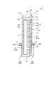
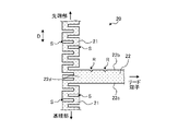
- FIG. 1 is a perspective view showing the overall configuration of the piezoelectric actuator according to the embodiment.
- FIG. 2 is a cross-sectional view taken along the line AA shown in FIG.
- FIG. 3 is a perspective view showing the internal structure of the piezoelectric actuator according to the embodiment.
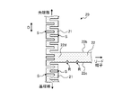
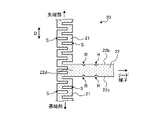
- FIG. 4 is an enlarged plan view showing the configuration of the electrode plate according to the embodiment.
- FIG. 5 is an enlarged plan view showing the shape of the recess located in the lead portion according to the embodiment.
- FIG. 6 is an enlarged plan view showing an example of the configuration of the recess and its periphery in the lead portion according to the embodiment.
- FIG. 7 is an enlarged plan view showing another example of the configuration of the recess and its periphery in the lead portion according to the embodiment.
- FIG. 1 is a perspective view showing the overall configuration of the piezoelectric actuator according to the embodiment.
- FIG. 2 is a cross-sectional view taken along the line AA shown in FIG.
- FIG. 3 is
- FIG. 8 is an enlarged plan view showing another example of the configuration of the recess and its periphery in the lead portion according to the embodiment.
- FIG. 9 is an enlarged plan view showing another example of the configuration of the recess and its periphery in the lead portion according to the embodiment.
- FIG. 10 is an enlarged perspective view showing another example of the configuration of the recess and its periphery in the lead portion according to the embodiment.
- FIG. 11 is an enlarged perspective view showing the configuration of the electrode plate according to the embodiment.
- FIG. 12 is an enlarged plan view showing the configuration of the electrode plate according to the first modification of the embodiment.
- FIG. 13 is an enlarged plan view showing the configuration of the electrode plate according to the second modification of the embodiment.
- FIG. 14 is an enlarged plan view showing the configuration of the electrode plate according to the modified example 3 of the embodiment.
- a piezoelectric actuator including a piezoelectric element laminated in a columnar shape and a metal case for accommodating the piezoelectric element so that both ends of the piezoelectric element abut against the inner wall is known.
- an electrode plate is joined to the side surface of a columnar piezoelectric element, and a driving voltage is applied to the piezoelectric element via the electrode plate.
- This electrode plate is composed of a main body portion joined to the side surface of the piezoelectric element and a lead portion that electrically connects the main body portion and the lead terminal.
- FIG. 1 is a perspective view showing the overall configuration of the piezoelectric actuator 1 according to the embodiment
- FIG. 2 is a cross-sectional view taken along the line AA shown in FIG.
- FIG. 3 is a perspective view showing the internal structure of the piezoelectric actuator 1 according to the embodiment.
- the piezoelectric actuator 1 includes a piezoelectric element 10, a pair of electrode plates 20, a pair of lead terminals 30, and a case 40.
- the pair of electrode plates 20 includes an electrode plate 20A and an electrode plate 20B
- the pair of lead terminals 30 includes a lead terminal 30A and a lead terminal 30B.
- the piezoelectric element 10 has a columnar shape.
- the piezoelectric element 10 has, for example, a rectangular parallelepiped shape having a length of 0.5 (mm) to 10 (mm), a width of 0.5 (mm) to 10 (mm), and a height of 1 (mm) to 100 (mm). ).
- the shape of the piezoelectric element 10 is not limited to a square columnar shape, and may be a hexagonal columnar column, an octagonal columnar column, a columnar column, or the like.
- the piezoelectric element 10 has a piezoelectric layer 11, an internal electrode layer 12, a planned breaking layer 13, and a pair of side electrodes 14.
- the pair of side electrode 14 includes the side electrode 14A and the side electrode 14B.
- the piezoelectric element 10 is configured by laminating the piezoelectric layer 11, the internal electrode layer 12, and the planned breaking layer 13 in a predetermined order along the stacking direction D.
- the stacking direction D of the piezoelectric element 10 coincides with the longitudinal direction of the piezoelectric element 10.
- the piezoelectric layer 11 is made of a piezoelectric material having piezoelectric properties, and is made of, for example, piezoelectric ceramics.
- the material of such piezoelectric ceramics is, for example, a perovskite-type oxide made of lead zirconate titanate (PbZrO 3 -PbTIO 3 ), lithium niobate (LiNbO 3 ), lithium tantalate (LiTaO 3 ), or the like.
- the average particle size of the piezoelectric ceramics is, for example, 1.6 ( ⁇ m) to 2.8 ( ⁇ m).
- the thickness of the piezoelectric layer 11 is, for example, 3 ( ⁇ m) to 250 ( ⁇ m).
- the internal electrode layer 12 is made of a conductive material and includes a plurality of first electrode layers 12a and a plurality of second electrode layers 12b.
- the first electrode layer 12a is electrically connected to the side electrode 14A.
- the side electrode 14A is arranged on one side surface 10a of the piezoelectric element 10. A predetermined positive voltage is applied to the first electrode layer 12a via the side electrode 14A.
- the second electrode layer 12b is electrically connected to the side electrode 14B.
- the side electrode 14B is arranged on the side surface 10b of the piezoelectric element 10 opposite to the side surface 10a.
- a predetermined negative voltage (or ground voltage) is applied to the second electrode layer 12b via the side electrode 14B.
- the first electrode layer 12a and the second electrode layer are arranged so that the piezoelectric layer 11 is arranged between the first electrode layer 12a and the second electrode layer 12b. 12b and the piezoelectric layer 11 are laminated. As a result, in the piezoelectric element 10, a driving voltage can be applied to the piezoelectric layer 11 by the first electrode layer 12a and the second electrode layer 12b.
- the piezoelectric element 10 is arranged on both ends of the active portion in which the piezoelectric layer 11 and the internal electrode layer 12 are alternately laminated and the stacking direction D in the active portion, and is piezoelectric. It is composed of an inactive portion having a body layer 11.
- the active portion is a portion that expands or contracts (hereinafter, also referred to as expansion and contraction) in the stacking direction D when a driving voltage is applied to the piezoelectric element 10 from the outside.
- the inactive portion is a portion that does not expand or contract even when a driving voltage is applied to the piezoelectric element 10 from the outside.
- the end portion of the case 40 on the substrate 41 side is the base end portion 10e of the piezoelectric element 10
- the end portion of the case 40 on the lid 43 side is the tip end portion 10f of the piezoelectric element 10.
- the base end portion 10e that is, the substrate 41
- the tip end portion 10f that is, the lid 43
- the material of the internal electrode layer 12 is, for example, a metal containing silver, silver-palladium, silver-platinum, copper, or the like as a main component.
- the internal electrode layer 12 can be formed, for example, by simultaneous firing with the piezoelectric layer 11.
- the thickness of the internal electrode layer 12 is, for example, 0.1 ( ⁇ m) to 5 ( ⁇ m).
- the planned break layer 13 is a layer for relaxing the stress generated by driving the piezoelectric element 10.
- Examples of the planned breakage layer 13 include a porous metal layer that does not function as the internal electrode layer 12, a metal layer that has been cracked in advance, and the like.
- the planned break layer 13 may be omitted.
- the pair of side electrode 14 includes the side electrode 14A located on the side surface 10a of the piezoelectric element 10 and the side electrode 14B located on the side surface 10b of the piezoelectric element 10.
- the side electrode 14 is arranged so as to cover the entire active portion of the piezoelectric element 10.
- the material of the side electrode 14 is, for example, a metal whose main component is silver or copper.
- a metallized layer made of a sintered body of the above metal and glass can be used.
- the thickness of the side electrode 14 is, for example, 5 ( ⁇ m) to 500 ( ⁇ m).
- the side surface 10c (see FIG. 3) and the side surface 10d (see FIG. 3) located between the side surface 10a and the side surface 10b of the piezoelectric element 10 are covered with an insulator. May be arranged. By arranging such a coating layer on the side surfaces 10c and 10d, it is possible to suppress creepage discharge between both poles generated when a high voltage is applied during driving.
- Examples of the insulator serving as the coating layer include ceramic materials.
- Examples of the ceramic material include a material that can follow the expansion and contraction of the piezoelectric element 10 when the piezoelectric actuator 1 is driven and is deformable by stress so that the coating layer itself does not peel off and a creepage discharge may occur. Be done.
- the coating layer include ceramic materials such as partially stabilized zirconia, Ln 1-X Si X AlO 3 + 0.5X , which undergoes local phase transformation and changes in volume when stress is generated. ..
- examples of the coating layer include piezoelectric materials such as barium titanate and lead zirconate titanate, in which the distance between ions in the crystal lattice changes so as to relieve the generated stress.
- the pair of electrode plates 20 includes the electrode plates 20A and the electrode plates 20B, and electrically connects the pair of side electrodes 14 and the pair of lead terminals 30, respectively.
- the electrode plate 20A electrically connects the side electrode 14A and the lead terminal 30A
- the electrode plate 20B electrically connects the side electrode 14B and the lead terminal 30B.
- the electrode plate 20 has a substantially T-shape, and has a main body portion 21 and a lead portion 22.
- the main body 21 is a portion extending in the stacking direction D of the piezoelectric element 10, and is electrically and mechanically connected to the side electrode 14 of the piezoelectric element 10.
- the main body portion 21 has the same size as the side electrode 14, and is joined to the side electrode 14 by a conductive bonding material.
- a conductive bonding material for example, an epoxy resin or a polyimide resin containing a metal powder having high conductivity such as Ag powder or Cu powder is used.
- the electrode plate 20 and the internal electrode layer 12 are electrically connected via the side electrode 14 , but since the electrode plate 20 and the internal electrode layer 12 can be sufficiently conductive. If so, the side electrode 14 may be omitted. In this case, the electrode plate 20 and the internal electrode layer 12 are directly connected.
- the electrode plate 20 and the internal electrode layer 12 can be electrically and stably connected. Therefore, according to the embodiment, the reliability of the piezoelectric actuator 1 can be improved.
- the lead portion 22 is a portion extending in a direction intersecting the stacking direction D, and is electrically and mechanically connected to the lead terminal 30.
- the lead portion 22 is drawn while bending from one side surface of the piezoelectric element 10 to which the main body portion 21 is joined toward the adjacent side surface.
- the lead portion 22 is drawn while bending from the side surface 10a toward the adjacent side surface 10c.
- the lead portion 22 is directed from the side surface 10b toward the adjacent side surface 10d, similarly to the electrode plate 20A. It is drawn around while bending.
- the material of the electrode plate 20 is, for example, a metal such as copper, iron, stainless steel, or phosphor bronze.
- the width of the electrode plate 20 is, for example, 0.5 (mm) to 10 (mm), and the thickness of the electrode plate 20 is, for example, 0.01 (mm) to 1.0 (mm).
- the surface of the electrode plate 20 may be coated with a plating film M (see FIG. 10) such as tin plating or silver plating in order to improve electrical conductivity and thermal conductivity.
- the pair of lead terminals 30 includes the lead terminals 30A and the lead terminals 30B, and are arranged so as to face the side surfaces 10c and 10d of the piezoelectric element 10, respectively.
- the lead terminal 30A is arranged to face the side surface 10c of the piezoelectric element 10
- the lead terminal 30B is arranged to face the side surface 10d of the piezoelectric element 10.
- a hole portion 22a1 (see FIG. 11) is arranged at the tip portion 22a of the electrode plate 20 that is routed from one side surface of the piezoelectric element 10 toward the adjacent side surface. Then, the lead terminal 30 is inserted into the hole portion 22a1 of the tip portion 22a and is joined by the conductive joining material 31. As a result, the electrode plate 20 and the lead terminal 30 are electrically and mechanically connected.
- the lead portion 22 of the electrode plate 20 since the lead portion 22 of the electrode plate 20 has a plurality of bent portions 22e (see FIG. 11), the vibration transmitted through the electrode plate 20 can be reduced. Further, in the embodiment, the lead portion 22 is long drawn from one side surface of the piezoelectric element 10 toward the adjacent side surface, so that the vibration transmitted through the electrode plate 20 can be further reduced.
- the case 40 houses the piezoelectric element 10 and the electrode plate 20 inside.
- the case 40 has a substrate 41, a tubular body 42, and a lid body 43.
- the substrate 41 is columnar (for example, columnar) and has a widened portion 41a at one end (upper side in FIG. 2).
- end surface 41b on the widening portion 41a side is in contact with the base end portion 10e of the piezoelectric element 10.
- the end face 41b of the substrate 41 and the base end portion 10e of the piezoelectric element 10 may be joined by a joining material (not shown).
- the substrate 41 is provided with a pair of through holes (not shown) penetrating between the end surface 41b and the end surface 41c on the opposite side of the end surface 41b, and the pair of lead terminals 30 are arranged in the pair of through holes. Are inserted respectively.
- the lead terminal 30 is fixed to the substrate 41 by filling the gap between the through hole of the substrate 41 and the lead terminal 30 with an insulating material (for example, soft glass). Further, the lead terminal 30 inserts the substrate 41 from the inside of the case 40 and projects outward from the end surface 41c of the substrate 41 (see FIG. 1).
- an insulating material for example, soft glass
- the tubular body 42 has a tubular shape (for example, a cylindrical shape). Further, the tubular body 42 has a bellows shape, and the axial direction of the cylinder coincides with the stacking direction D of the piezoelectric element 10. As a result, the tubular body 42 can expand and contract in the axial direction following the expansion and contraction of the piezoelectric element 10 in the stacking direction D.
- the tubular body 42 has a predetermined spring coefficient so as to be able to follow the expansion and contraction of the piezoelectric element 10.
- the spring coefficient of the tubular body 42 can be adjusted by the thickness of the tubular body 42, the groove shape of the tubular body 42, the number of grooves of the tubular body 42, and the like.
- the thickness of the tubular body 42 is, for example, 0.1 (mm) to 0.5 (mm), and the diameter of the tubular body 42 is, for example, 5 (mm) to 50 (mm).
- the tubular body 42 has a flange portion 42a that spreads like a trumpet toward the outside in the radial direction at the end portion on the side of the substrate 41. Then, between the flange portion 42a of the tubular body 42 and the widening portion 41a of the substrate 41, for example, the piezoelectric element 10 is welded with a compressive load applied.
- the tubular body 42 is formed, for example, by preparing a seamless pipe having a predetermined shape and then processing the seamless pipe into a bellows shape by rolling or hydrostatic pressing.
- the lid 43 has a cylindrical shape (for example, a cylindrical shape) with one end closed. Further, the outer diameter of the lid 43 is slightly smaller than the inner diameter of the end portion 42b of the tubular body 42 opposite to the flange portion 42a. Then, the lid 43 is fitted into the end 42b, and the inner wall of the end 42b and the side wall of the lid 43 are welded and fixed, for example.
- the inner bottom surface 43a of the lid 43 is in contact with the tip portion 10f of the piezoelectric element 10.
- the inner bottom surface 43a of the lid 43 and the tip portion 10f of the piezoelectric element 10 may be joined by a joining material (not shown).
- FIG. 4 is an enlarged plan view showing the configuration of the electrode plate 20 according to the embodiment.
- the electrode plate 20 has a substantially T-shape, and has a main body portion 21 extending in the stacking direction D of the piezoelectric element 10 and a lead portion 22 extending in a direction intersecting the stacking direction D.
- the main body 21 of the electrode plate 20 has a plurality of slits S.
- the slit S is cut out so as to extend along the width direction of the main body 21 (that is, the direction perpendicular to the stacking direction D), for example.
- the plurality of slits S are alternately cut out from both side portions of the main body portion 21 and are arranged side by side at substantially equal intervals along the stacking direction D. Further, the plurality of slits S all have substantially the same length.
- the length of the slit S is the length of the slit S in the notch direction (that is, the width direction of the main body 21).
- the length is set so that the tips overlap each other when viewed in the stacking direction D.
- overlapping means that the slits S adjacent to each other have regions facing each other when viewed in the stacking direction D.
- the main body portion 21 of the electrode plate 20 by arranging a plurality of slits S in the main body portion 21 of the electrode plate 20, the main body portion 21 can be expanded and contracted in the stacking direction D by following the expansion and contraction of the piezoelectric element 10 in the stacking direction D. .. Therefore, according to the embodiment, it is possible to prevent the electrode plate 20 from peeling off from the piezoelectric element 10.
- the lead portion 22 of the electrode plate 20 has a pair of side portions 22b and 22c.
- the side portion 22b is the side portion of the piezoelectric element 10 (see FIG. 3) on the tip end portion 10f (see FIG. 3) side
- the side portion 22c is the side of the piezoelectric element 10 on the base end portion 10e (see FIG. 3) side. It is a department.
- the lead portion 22 has a recess R recessed in the width direction of the lead portion 22 on at least one side portion (side portion 22c in FIG. 4).
- the width direction of the lead portion 22 is a direction perpendicular to the direction in which the lead portion 22 extends.
- the stress generated in the base end portion 22d of the lead portion 22 due to the expansion and contraction of the piezoelectric element 10 can be relaxed, so that the electrode plate 20 is suppressed from peeling from the piezoelectric element 10. can do.
- a plurality of recesses R may be arranged on one side portion of the lead portion 22.
- the lead portion 22 can be further easily deformed by following the expansion and contraction of the piezoelectric element 10 in the stacking direction D.
- the stress generated in the base end portion 22d of the lead portion 22 due to the expansion and contraction of the piezoelectric element 10 can be further relaxed, so that the electrode plate 20 is peeled off from the piezoelectric element 10. It can be further suppressed.
- FIG. 4 an example in which two concave portions R are arranged on one side portion is shown, but the number of concave portions R arranged on one side portion is not limited to two, and one concave portion R is provided. It may be arranged, or three or more recesses R may be arranged. Further, the plurality of recesses R provided on one side portion may all have substantially the same size, or may have different sizes.
- the recess R may be arranged at least on the side portion 22c on the proximal end portion 10e side of the piezoelectric element 10 among the pair of side portions 22b and 22c in the lead portion 22. As a result, it is possible to easily deform the side portion 22c on the base end portion 10e side to which a large tensile stress is applied when the piezoelectric element 10 is extended.
- the stress generated in the proximal end portion 22d of the lead portion 22 when the piezoelectric element 10 is extended can be relaxed, so that the electrode plate 20 is suppressed from peeling from the piezoelectric element 10. be able to.
- the recess R may be arranged at a position closer to the base end portion 22d of the lead portion 22 than the tip end portion 22a (see FIG. 3) of the lead portion 22.
- the stress generated in the base end portion 22d of the lead portion 22 due to the expansion and contraction of the piezoelectric element 10 can be further relaxed, so that the electrode plate 20 is peeled off from the piezoelectric element 10. It can be further suppressed.
- FIG. 5 is an enlarged plan view showing the shape of the recess R located in the lead portion 22 according to the embodiment.
- the recess R according to the embodiment may have a substantially V-shape.
- the lead portion 22 can be further easily deformed by following the expansion and contraction of the piezoelectric element 10 in the stacking direction D.
- the stress generated in the base end portion 22d of the lead portion 22 due to the expansion and contraction of the piezoelectric element 10 can be further relaxed, so that the electrode plate 20 is peeled off from the piezoelectric element 10. It can be further suppressed.
- the bottom Ra of the recess R may have an R shape.
- the reliability of the piezoelectric actuator 1 can be improved.
- the volume resistance of the lead portion 22 becomes large, so that local heat is generated in the lead portion 22. May occur. That is, when the slit S extending long in the notch direction is arranged in the lead portion 22, the reliability of the piezoelectric actuator 1 may decrease.
- the recess R having a shallow depth is arranged in the lead portion 22, local heat generation in the lead portion 22 can be suppressed, so that the reliability of the piezoelectric actuator 1 is improved. Can be maintained.
- the recess R of the present disclosure has, for example, a ratio of the depth to the width of twice or less. As a result, local heat generation in the lead portion 22 can be suppressed, so that the reliability of the piezoelectric actuator 1 can be maintained satisfactorily.
- the depth of the recess R is preferably 1/10 or less of the width of the lead portion 22.
- the width of the recess R may be in the range of, for example, 0.01 to 0.1 (mm), and the depth of the recess R may be, for example, 0.05 to 1.0 (mm). ) May be the range.
- FIG. 6 is an enlarged plan view showing an example of the configuration of the recess R and its periphery in the lead portion 22 according to the embodiment.
- the side portion 22c in which the recess R is located in the lead portion 22 includes a first region 22c1 sandwiched between the pair of recesses R and a second region 22c2 other than the first region 22c1.
- the first region 22c1 and the second region 22c2 may be substantially flush with each other in the vicinity of the pair of recesses R in the side portion 22c.
- the lead portion 22 according to the embodiment is not limited to the case where the first region 22c1 and the second region 22c2 are substantially flush with each other.
- 7 to 9 are enlarged plan views showing another example of the configuration of the recess R and its surroundings in the lead portion 22 according to the embodiment.
- the first region 22c1 may protrude outward with respect to the second region 22c2 in the vicinity of the pair of recesses R in the side portion 22c.
- the first region 22c1 may be retracted inward with respect to the second region 22c2 in the vicinity of the pair of recesses R in the side portion 22c.
- the first region 22c1 retracts to the bottom Ra of the recess R, so that the pair of recesses R are formed as shown in FIG. It may be an integrated substantially trapezoidal concave portion R.
- FIG. 10 is an enlarged perspective view showing another example of the configuration of the recess R and its periphery in the lead portion 22 according to the embodiment.
- a plating film M for improving electrical conductivity and thermal conductivity is arranged, including the surface of the lead portion 22.
- dot-shaped hatching is attached to the portion where the plating film M is arranged.
- the side portion 22c of the lead portion 22 may have a portion without the plating film M in the first region 22c1 between the adjacent recesses R.
- the entire first region 22c1 may be a portion without the plating film M.
- the lead portion 22 is more easily deformed by following the expansion and contraction of the piezoelectric element 10 in the stacking direction D. be able to. Therefore, according to the embodiment, it is possible to further suppress the peeling of the electrode plate 20 from the piezoelectric element 10.
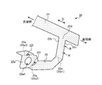
- FIG. 11 is an enlarged perspective view showing the configuration of the electrode plate 20 according to the embodiment. As shown in FIG. 11, a plurality of bent portions 22e are arranged in the lead portion 22 from the base end portion 22d to the tip end portion 22a.
- the bent portion 22e1 closest to the base end portion 22d is a bent portion arranged along a corner portion located between adjacent side surfaces in the piezoelectric element 10 (see FIG. 3). be.
- bent portion 22e2 located next to the bent portion 22e1 with the base end portion 22d as a reference is located around the hole portion 22a1 in the tip portion 22a, and is a bent portion for making the tip portion 22a substantially horizontal. Is.
- bent portion 22e3 located next to the bent portion 22e2 with respect to the base end portion 22d is located around the hole portion 22a1 at the tip portion 22a and faces the bent portion 22e2 via the hole portion 22a1. Located in.
- the recess R located on the side portion 22c of the lead portion 22 may be arranged between the base end portion 22d and the bent portion 22e1.
- the recess R by arranging the recess R at a position close to the base end portion 22d adjacent to the main body portion 21 where peeling occurs, it is complicated to follow the expansion and contraction of the piezoelectric element 10 in the stacking direction D via the bending portion 22e1.
- the stress generated in the lead that has changed in any direction can be relaxed, and the electrode plate 20 can be peeled off from the piezoelectric element 10. It can be further suppressed.
- the stress generated in the base end portion 22d of the lead portion 22 due to the expansion and contraction of the piezoelectric element 10 can be further relaxed, so that the electrode plate 20 is peeled off from the piezoelectric element 10. It can be further suppressed.
- the bent portions 22e2 and 22e3 located around the hole portion 22a1 may have the through hole 22f.
- the reliability of the piezoelectric actuator 1 can be improved.
- the joining material 31 may or may not enter the through hole 22f.
- FIG. 12 is an enlarged plan view showing the configuration of the electrode plate 20 according to the first modification of the embodiment.
- the arrangement of the recess R is different from that of the above-described embodiment.
- the recess R is not the side portion 22c of the piezoelectric element 10 (see FIG. 3) on the base end portion 10e (see FIG. 3) side of the lead portion 22, but the tip portion 10f of the piezoelectric element 10. It is arranged on the side portion 22b on the (see FIG. 3) side.
- FIG. 13 is an enlarged plan view showing the configuration of the electrode plate 20 according to the second modification of the embodiment. As shown in FIG. 13, in the modified example 2, the lead portion 22 has recesses R on both side portions 22b and 22c, respectively.
- the recesses R located on both side portions 22b and 22c of the lead portion 22 may be located facing each other. In this way, by locating the recess R so as to face both side portions 22b and 22c, twisting is likely to occur starting from the region connecting the opposing recesses R, and even with a weak force, the lead portion is likely to occur in the vicinity of the recess R. 22 can be easily deformed.
- the recesses R facing each other on both side portions 22b and 22c may have substantially the same size or may have different sizes.
- FIG. 14 is an enlarged plan view showing the configuration of the electrode plate 20 according to the modified example 3 of the embodiment.
- the lead portion 22 has recesses R in both side portions 22b and 22c, respectively, as in the above-described modified example 2.
- the base end portion 10e (see FIG. 3) of the piezoelectric element 10 is more than the recess R located on the side portion 22b on the tip portion 10f (see FIG. 3) side of the piezoelectric element 10 (see FIG. 3).
- the recess R located on the side portion 22c on the) side is deeper.
- the side portion 22c on the base end portion 10e side to which a large tensile stress is applied when the piezoelectric element 10 is extended can be further easily deformed.
- the stress generated in the base end portion 22d of the lead portion 22 when the piezoelectric element 10 is extended can be further relaxed, so that the electrode plate 20 is peeled off from the piezoelectric element 10. It can be further suppressed.
- the piezoelectric actuator 1 includes a piezoelectric element 10 laminated in a columnar shape, and an electrode plate 20 located on the side surfaces 10a and 10c of the piezoelectric element 10 and electrically connected to the internal electrode layer 12 of the piezoelectric element 10. , Equipped with.
- the electrode plate 20 has a main body portion 21 extending in the stacking direction D of the piezoelectric element 10 and a lead portion 22 extending in a direction intersecting the stacking direction D and electrically connected to the lead terminal 30.
- the lead portion 22 has a recess R recessed in the width direction of the lead portion 22 in at least one side portion 22c (22b). As a result, it is possible to prevent the electrode plate 20 from peeling off from the piezoelectric element 10.
- the recess R is arranged at a position closer to the base end portion 22d of the lead portion 22 than the tip portion 22a of the lead portion 22. As a result, it is possible to further suppress the peeling of the electrode plate 20 from the piezoelectric element 10.
- the lead portion 22 has recesses R on both side portions 22b and 22c, respectively. As a result, it is possible to further suppress the peeling of the electrode plate 20 from the piezoelectric element 10.
- the recesses R located on both side portions 22b and 22c of the lead portion 22 are located facing each other. As a result, it is possible to further suppress the peeling of the electrode plate 20 from the piezoelectric element 10.
- the recess R located on the side portion 22b on the base end portion 10e side of the piezoelectric element 10 is larger than the recess R located on the side portion 22c on the tip end portion 10f side of the piezoelectric element 10. deep. As a result, it is possible to further suppress the peeling of the electrode plate 20 from the piezoelectric element 10.
- the concave portion R has a substantially V-shape. As a result, it is possible to further suppress the peeling of the electrode plate 20 from the piezoelectric element 10.
- the bottom Ra of the recess R has an R shape. Therefore, the reliability of the piezoelectric actuator 1 can be improved.
- the lead portion 22 has a plurality of recesses R in one side portion 22c (22b), and the one side portion 22c (22b) is between adjacent recesses R.
- the region (first region 22c1) has a portion without the plating film M. As a result, it is possible to further suppress the peeling of the electrode plate 20 from the piezoelectric element 10.
- the lead portion 22 has a plurality of bent portions 22e and a hole portion 22a1 through which the lead terminal 30 is inserted, and the bent portion 22e2 located around the hole portion 22a1.
- the 22e3 has a through hole 22f.
- Piezoelectric actuator 10 Piezoelectric element 10a-10d Side surface 10e Base end 10f Tip 11 Piezoelectric layer 12 Internal electrode layer 14, 14A, 14B Side electrode 20, 20A, 20B Electrode plate 21 Main body 22 Lead 22a Tip 22a1 hole Part 22b, 22c Side part 22c1 First area 22c2 Second area 22d Base end part 22e, 22e1 to 22e3 Bending part 22f Through hole 30, 30A, 30B Lead terminal 40 Case D Stacking direction S Slit
Landscapes
- General Electrical Machinery Utilizing Piezoelectricity, Electrostriction Or Magnetostriction (AREA)
Abstract
圧電アクチュエータ(1)は、柱状に積層される圧電素子(10)と、圧電素子(10)の側面(10a、10c)に位置し、圧電素子(10)の内部電極層(12)に電気的に接続される電極板(20)と、を備える。電極板(20)は、圧電素子(10)の積層方向(D)に延びる本体部(21)と、積層方向(D)と交差する方向に延び、リード端子(30)に電気的に接続されるリード部(22)と、を有する。リード部(22)は、リード部(22)の幅方向に凹む凹部(R)を少なくとも一方の側部(22c)に有する。
Description
開示の実施形態は、圧電アクチュエータに関する。
従来、柱状に積層された圧電素子と、この圧電素子における両方の端部が内壁に当接するように圧電素子を収容する金属ケースと、を備えた圧電アクチュエータが知られている(例えば、特許文献1参照)。
この圧電アクチュエータでは、たとえば、柱状の圧電素子の側面に電極板が接合され、かかる電極板を介して圧電素子に駆動電圧が印加される。この電極板は、圧電素子の側面に接合される本体部と、かかる本体部とリード端子とを電気的に接続するリード部とで構成される。
実施形態の一態様は、圧電素子から電極板が剥離することを抑制することができる圧電アクチュエータを提供することを目的とする。
実施形態の一態様に係る圧電アクチュエータは、柱状に積層される圧電素子と、前記圧電素子の側面に位置し、前記圧電素子の内部電極層に電気的に接続される電極板と、を備える。前記電極板は、前記圧電素子の積層方向に延びる本体部と、前記積層方向と交差する方向に延び、リード端子に電気的に接続されるリード部と、を有する。前記リード部は、前記リード部の幅方向に凹む凹部を少なくとも一方の側部に有する。
以下、添付図面を参照して、本願の開示する圧電アクチュエータの実施形態について説明する。なお、以下に示す実施形態により本開示が限定されるものではない。また、図面は模式的なものであり、各要素の寸法の関係、各要素の比率などは、現実と異なる場合があることに留意する必要がある。さらに、図面の相互間においても、互いの寸法の関係や比率が異なる部分が含まれている場合がある。
従来、柱状に積層された圧電素子と、この圧電素子における両方の端部が内壁に当接するように圧電素子を収容する金属ケースと、を備えた圧電アクチュエータが知られている。
この圧電アクチュエータでは、たとえば、柱状の圧電素子の側面に電極板が接合され、かかる電極板を介して圧電素子に駆動電圧が印加される。この電極板は、圧電素子の側面に接合される本体部と、かかる本体部とリード端子とを電気的に接続するリード部とで構成される。
しかしながら、従来技術では、圧電素子の伸縮動作に対してリード部が十分に変形することができず、本体部が圧電素子から剥離してしまうという問題があった。
そこで、上述の問題点を克服し、圧電素子から電極板が剥離することを抑制することができる技術の実現が期待されている。
<圧電アクチュエータの全体構成>
最初に、実施形態に係る圧電アクチュエータ1の全体構成について、図1~図3を参照しながら説明する。図1は、実施形態に係る圧電アクチュエータ1の全体構成を示す斜視図であり、図2は、図1に示すA-A線の矢視断面図である。また、図3は、実施形態に係る圧電アクチュエータ1の内部構造を示す斜視図である。
最初に、実施形態に係る圧電アクチュエータ1の全体構成について、図1~図3を参照しながら説明する。図1は、実施形態に係る圧電アクチュエータ1の全体構成を示す斜視図であり、図2は、図1に示すA-A線の矢視断面図である。また、図3は、実施形態に係る圧電アクチュエータ1の内部構造を示す斜視図である。
図1~図3に示すように、実施形態に係る圧電アクチュエータ1は、圧電素子10と、一対の電極板20と、一対のリード端子30と、ケース40とを備える。なお、一対の電極板20は電極板20Aと電極板20Bとを含み、一対のリード端子30はリード端子30Aとリード端子30Bとを含む。
図3に示すように、圧電素子10は、柱状形状を有する。圧電素子10は、たとえば、縦0.5(mm)~10(mm)、横0.5(mm)~10(mm)、高さ1(mm)~100(mm)の四角柱状(直方体状)である。なお、圧電素子10の形状は四角柱状に限られず、六角柱状、八角柱状または円柱状などであってもよい。
図2に示すように、圧電素子10は、圧電体層11と、内部電極層12と、予定破断層13と、一対の側面電極14とを有する。なお、一対の側面電極14は、側面電極14Aと側面電極14Bとを含む。
圧電素子10は、圧電体層11と、内部電極層12と、予定破断層13とを積層方向Dに沿って所定の順序で積層して構成される。本開示では、圧電素子10の積層方向Dが圧電素子10の長手方向と一致している。
圧電体層11は、圧電特性を有する圧電材料で構成され、たとえば、圧電セラミックスで構成される。かかる圧電セラミックスの材質は、たとえば、チタン酸ジルコン酸鉛(PbZrO3-PbTiO3)からなるペロブスカイト型酸化物、ニオブ酸リチウム(LiNbO3)またはタンタル酸リチウム(LiTaO3)などである。
かかる圧電セラミックスの平均粒径は、たとえば、1.6(μm)~2.8(μm)である。また、圧電体層11の厚みは、たとえば、3(μm)~250(μm)である。
内部電極層12は、導電性材料で構成され、複数の第1電極層12aと複数の第2電極層12bとを含む。第1電極層12aは、側面電極14Aに電気的に接続される。かかる側面電極14Aは、圧電素子10の1つの側面10aに配置される。第1電極層12aには、かかる側面電極14Aを介して、所定の正電圧が印加される。
第2電極層12bは、側面電極14Bに電気的に接続される。かかる側面電極14Bは、圧電素子10における側面10aとは反対側の側面10bに配置される。第2電極層12bには、かかる側面電極14Bを介して、所定の負電圧(またはグランド電圧)が印加される。
図2に示すように、圧電素子10の内部では、第1電極層12aと第2電極層12bとの間に圧電体層11が配置されるように、第1電極層12a、第2電極層12bおよび圧電体層11が積層される。これにより、圧電素子10では、第1電極層12aおよび第2電極層12bによって圧電体層11に駆動電圧を印加することができる。
そして、実施形態に係る圧電素子10は、圧電体層11と内部電極層12とを交互に複数積層して構成される活性部と、かかる活性部における積層方向Dの両端側に配置され、圧電体層11を有する不活性部とで構成される。
活性部は、外部から圧電素子10に駆動電圧が印加されることによって、積層方向Dに伸長または収縮(以下、伸縮とも呼称する。)する部位である。一方で、不活性部は、外部から圧電素子10に駆動電圧が印加された場合でも伸縮しない部位である。
また、本開示では、ケース40の基体41側の端部を圧電素子10の基端部10eとし、ケース40の蓋体43側の端部を圧電素子10の先端部10fとする。
そして、実施形態に係る圧電アクチュエータ1では、圧電素子10の基端部10e(すなわち、基体41)が固定されるとともに、圧電素子10の先端部10f(すなわち、蓋体43)が積層方向Dに沿って変位する。
内部電極層12の材質は、たとえば、銀、銀-パラジウム、銀-白金または銅などを主成分とする金属である。内部電極層12は、たとえば、圧電体層11との同時焼成により形成することができる。内部電極層12の厚みは、たとえば、0.1(μm)~5(μm)である。
予定破断層13は、圧電素子10の駆動によって生じる応力を緩和するための層である。予定破断層13としては、たとえば、内部電極層12として機能しない多孔質な金属層、またはあらかじめ亀裂の入った金属層などが挙げられる。なお、実施形態に係る圧電素子10において、予定破断層13は省略されてもよい。
一対の側面電極14は、上述したように、圧電素子10の側面10aに位置する側面電極14Aと、圧電素子10の側面10bに位置する側面電極14Bとを含む。側面電極14は、圧電素子10の活性部全体に渡るように配置される。
側面電極14の材質は、たとえば、銀または銅などを主成分とする金属である。側面電極14には、たとえば、上記の金属とガラスとの焼結体からなるメタライズ層を用いることができる。側面電極14の厚みは、たとえば、5(μm)~500(μm)である。
なお、本開示では図示していないが、圧電素子10の側面10aと側面10bとの間に位置する側面10c(図3参照)および側面10d(図3参照)には、絶縁体からなる被覆層が配置されていてもよい。かかる被覆層を側面10c、10dに配置することにより、駆動時に高電圧をかけた際に発生する両極間での沿面放電を抑制することができる。
この被覆層となる絶縁体としては、たとえば、セラミック材料が挙げられる。かかるセラミックス材料としては、たとえば、圧電アクチュエータ1を駆動した際の圧電素子10の伸縮に追随でき、かかる被覆層自体が剥がれて沿面放電が生じるおそれのないように、応力によって変形可能な材料が挙げられる。
具体的には、被覆層としては、応力が生じると局所的に相変態して体積変化して変形可能な部分安定化ジルコニア、Ln1-XSiXAlO3+0.5Xなどのセラミック材料が挙げられる。なお、Lnは、Sn,Y,La,Ce,Pr,Nd,Pm,Sm,Eu,Gd,Tb,Dy,Ho,Er,TmおよびYbのうちから選ばれるいずれか少なくとも一種を示し、x=0.01~0.3である。
あるいは、被覆層としては、生じた応力を緩和するように結晶格子内のイオン間距離が変化するチタン酸バリウム、チタン酸ジルコン酸鉛などの圧電材料が挙げられる。
一対の電極板20は、電極板20Aと電極板20Bとを含み、一対の側面電極14と一対のリード端子30との間をそれぞれ電気的に接続する。具体的には、電極板20Aは、側面電極14Aとリード端子30Aとの間を電気的に接続し、電極板20Bは、側面電極14Bとリード端子30Bとの間を電気的に接続する。
図3に示すように、電極板20は、略T字形状を有し、本体部21と、リード部22とを有する。本体部21は、圧電素子10の積層方向Dに延びる部位であり、圧電素子10の側面電極14に電気的および機械的に接続される。
本体部21は、側面電極14と同程度の大きさを有し、かかる側面電極14に導電性接合材によって接合される。かかる導電性接合材としては、たとえば、Ag粉末やCu粉末などの高い導電性を有する金属粉末を含んだエポキシ樹脂またはポリイミド樹脂などが用いられる。
なお、本開示では、側面電極14を介して電極板20と内部電極層12とが電気的に接続される例について示したが、電極板20と内部電極層12との導通が十分にとれるのであれば側面電極14は省略されてもよい。この場合、電極板20と内部電極層12とが直接接続される。
一方で、側面電極14を配置することにより、電極板20と内部電極層12とを電気的に安定して接続することができる。したがって、実施形態によれば、圧電アクチュエータ1の信頼性を向上させることができる。
リード部22は、積層方向Dと交差する方向に延びる部位であり、リード端子30に電気的および機械的に接続される。かかるリード部22は、本体部21が接合された圧電素子10の1つの側面から隣の側面に向かって屈曲しながら引き回されている。
たとえば、図3に示すように、圧電素子10の側面10aに接合される電極板20Aでは、リード部22が側面10aから隣の側面10cに向かって屈曲しながら引き回されている。
また、図3には完全に図示されていないが、圧電素子10の側面10bに接合される電極板20Bでは、電極板20Aと同様に、リード部22が側面10bから隣の側面10dに向かって屈曲しながら引き回されている。
電極板20の材質は、たとえば、銅、鉄、ステンレス、リン青銅などの金属である。電極板20の幅は、たとえば、0.5(mm)~10(mm)であり、電極板20の厚みは、たとえば、0.01(mm)~1.0(mm)である。電極板20の表面には、電気伝導性や熱伝導性を向上させるため、スズめっきまたは銀めっきなどのめっき膜M(図10参照)が施されていてもよい。
一対のリード端子30は、図3に示すように、リード端子30Aとリード端子30Bとを含み、圧電素子10の側面10c、10dにそれぞれ向かい合って配置される。具体的には、リード端子30Aは圧電素子10の側面10cに向かい合って配置され、リード端子30Bは圧電素子10の側面10dに向かい合って配置される。
また、圧電素子10の1つの側面から隣の側面に向かって引き回される電極板20の先端部22aには、孔部22a1(図11参照)が配置される。そして、先端部22aの孔部22a1にリード端子30が挿入されて、導電性の接合材31によって接合される。これにより、電極板20とリード端子30とが電気的および機械的に接続される。
実施形態では、電極板20のリード部22に複数の屈曲部22e(図11参照)があることで、電極板20を介して伝達される振動を低減することができる。また、実施形態では、リード部22が圧電素子10の1つの側面から隣の側面に向かって長く引き回されることにより、電極板20を介して伝達される振動をさらに低減することができる。
ケース40は、図2に示すように、圧電素子10および電極板20を内部に収容する。ケース40は、基体41と、筒体42と、蓋体43とを有する。基体41は、柱状(たとえば、円柱状)であり、幅が広がった拡幅部41aを一方側(図2では上側)の端部に有する。
また、かかる拡幅部41a側の端面41bは、圧電素子10の基端部10eと接する。なお、基体41の端面41bと圧電素子10の基端部10eとは、図示しない接合材で接合されていてもよい。
また、基体41には、端面41bと、かかる端面41bの反対側の端面41cとの間を貫通する一対の貫通孔(図示せず)が配置され、かかる一対の貫通孔に一対のリード端子30がそれぞれ挿通される。
そして、基体41の貫通孔とリード端子30との間の隙間に絶縁性材料(たとえば、軟質ガラスなど)が充填されることにより、基体41に対してリード端子30が固定される。さらに、リード端子30は、ケース40の内部から基体41を挿通して、基体41の端面41cから外方に突出する(図1参照)。
筒体42は、筒形状(たとえば、円筒形状)を有する。また、筒体42は、ベロー(蛇腹)形状を有するとともに、筒の軸方向が圧電素子10の積層方向Dと一致している。これにより、筒体42は、圧電素子10の積層方向Dへの伸縮に追従して、軸方向に伸縮することができる。
また、筒体42は、圧電素子10の伸縮に追従することができるように、所定のバネ係数を有する。かかる筒体42のバネ係数は、筒体42の厚み、筒体42の溝形状および筒体42の溝の本数などにより調整可能である。筒体42の厚みは、たとえば、0.1(mm)~0.5(mm)であり、筒体42の直径は、たとえば、5(mm)~50(mm)である。
また、筒体42は、基体41側の端部に、径方向外側に向かってラッパ状に広がる鍔部42aを有する。そして、筒体42の鍔部42aと基体41の拡幅部41aとの間は、たとえば、圧電素子10に圧縮荷重をかけた状態で溶接される。
筒体42は、たとえば、所定の形状のシームレス管を準備した後、かかるシームレス管を圧延加工や静水圧プレスなどによりベロー(蛇腹)形状に加工することで形成される。
蓋体43は、一端が塞がった筒形状(たとえば、円筒形状)である。また、蓋体43の外径は、筒体42における鍔部42aとは反対側の端部42bの内径よりもわずかに小さい。そして、かかる端部42bに蓋体43が嵌め込まれ、端部42bの内壁と蓋体43の側壁とが、たとえば溶接されて固定される。
また、蓋体43の内底面43aは、圧電素子10の先端部10fと接する。なお、蓋体43の内底面43aと圧電素子10の先端部10fとは、図示しない接合材で接合されていてもよい。
<電極板の構成>
つづいて、実施形態に係る電極板20の詳細な構成について、図4~図11を参照しながら説明する。図4は、実施形態に係る電極板20の構成を示す拡大平面図である。上述したように、電極板20は、略T字形状を有し、圧電素子10の積層方向Dに延びる本体部21と、積層方向Dと交差する方向に延びるリード部22とを有する。
つづいて、実施形態に係る電極板20の詳細な構成について、図4~図11を参照しながら説明する。図4は、実施形態に係る電極板20の構成を示す拡大平面図である。上述したように、電極板20は、略T字形状を有し、圧電素子10の積層方向Dに延びる本体部21と、積層方向Dと交差する方向に延びるリード部22とを有する。
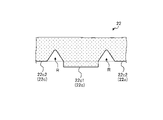
そして、図4に示すように、実施形態では、電極板20の本体部21が複数のスリットSを有する。かかるスリットSは、たとえば、本体部21の幅方向(すなわち、積層方向Dとは垂直な方向)に沿って延びるように切り欠かれる。
複数のスリットSは、本体部21における両方の側部から交互に切り欠かれるとともに、積層方向Dに沿って略均等な間隔で並んで配置される。また、複数のスリットSは、すべて略等しい長さを有する。なお、スリットSの長さとは、スリットSの切り欠き方向(すなわち、本体部21の幅方向)における長さのことである。
さらに、複数のスリットSでは、積層方向Dに見て先端同士が重なり合うように長さが設定される。ここで、重なり合うとは、積層方向Dに見た場合において、互いに隣接するスリットS同士が互いに対向する領域を有することを意味している。
実施形態では、電極板20の本体部21に複数のスリットSを配置することにより、圧電素子10の積層方向Dへの伸縮に追従して、本体部21を積層方向Dに伸縮させることができる。したがって、実施形態によれば、圧電素子10から電極板20が剥離することを抑制することができる。
電極板20のリード部22は、一対の側部22b、22cを有する。側部22bは、圧電素子10(図3参照)の先端部10f(図3参照)側の側部であり、側部22cは、圧電素子10の基端部10e(図3参照)側の側部である。
ここで、実施形態では、リード部22が、かかるリード部22の幅方向に凹む凹部Rを少なくとも一方の側部(図4では側部22c)に有する。なお、リード部22の幅方向とは、リード部22が延びる方向とは垂直な方向である。
これにより、圧電素子10の積層方向Dへの伸縮に追従して、凹部Rを起点としたひねりが生じ、リード部22を変形しやすくすることができる。したがって、実施形態によれば、圧電素子10の伸縮に起因してリード部22の基端部22dに発生する応力を緩和することができるため、圧電素子10から電極板20が剥離することを抑制することができる。
また、実施形態では、リード部22の1つの側部に、複数の凹部Rを配置してもよい。これにより、圧電素子10の積層方向Dへの伸縮に追従して、リード部22をさらに変形しやすくすることができる。
したがって、実施形態によれば、圧電素子10の伸縮に起因してリード部22の基端部22dに発生する応力をさらに緩和することができるため、圧電素子10から電極板20が剥離することをさらに抑制することができる。
なお、図4の例では、1つの側部に2つの凹部Rを配置した例について示したが、1つの側部に配置される凹部Rの数は2つに限られず、1つの凹部Rを配置してもよいし、3つ以上の凹部Rを配置してもよい。また、1つの側部に設けられる複数の凹部Rは、すべて略等しいサイズであってもよいし、それぞれ異なるサイズであってもよい。
また、実施形態では、リード部22における一対の側部22b、22cのうち、少なくとも圧電素子10の基端部10e側の側部22cに凹部Rを配置してもよい。これにより、圧電素子10が伸長した場合に大きな引張応力が加わる基端部10e側の側部22cを変形しやすくすることができる。
したがって、実施形態によれば、圧電素子10が伸長する際にリード部22の基端部22dに発生する応力を緩和することができるため、圧電素子10から電極板20が剥離することを抑制することができる。
また、実施形態では、凹部Rが、リード部22の先端部22a(図3参照)よりもリード部22の基端部22dに近い位置に配置されてもよい。このように、剥離が生じる本体部21に隣接する基端部22dに近い位置に凹部Rを配置することにより、圧電素子10の伸縮に対してリード部22を変形しやすくすることができる。
したがって、実施形態によれば、圧電素子10の伸縮に起因してリード部22の基端部22dに発生する応力をさらに緩和することができるため、圧電素子10から電極板20が剥離することをさらに抑制することができる。
図5は、実施形態に係るリード部22に位置する凹部Rの形状を示す拡大平面図である。図5に示すように、実施形態に係る凹部Rは、略V字形状を有してもよい。これにより、圧電素子10の積層方向Dへの伸縮に追従して、リード部22をさらに変形しやすくすることができる。
したがって、実施形態によれば、圧電素子10の伸縮に起因してリード部22の基端部22dに発生する応力をさらに緩和することができるため、圧電素子10から電極板20が剥離することをさらに抑制することができる。
また、実施形態では、図5に示すように、凹部Rの底部RaがR形状であってもよい。これにより、圧電素子10の伸縮によってリード部22が変形する際に、凹部Rの底部Raに応力が集中して、かかる底部Raからリード部22が切れたりクラックが生じたりすることを抑制することができる。
したがって、実施形態によれば、圧電アクチュエータ1の信頼性を向上させることができる。
なお、もし仮に深さが浅い凹部Rではなく、切り欠き方向に長く延びるスリットSをリード部22に配置した場合、リード部22の体積抵抗が大きくなることから、リード部22において局所的な発熱が生じる場合がある。すなわち、切り欠き方向に長く延びるスリットSをリード部22に配置した場合、圧電アクチュエータ1の信頼性が低下してしまう恐れがある。
一方で、実施形態では、深さが浅い凹部Rをリード部22に配置していることから、リード部22における局所的な発熱を抑制することができるため、圧電アクチュエータ1の信頼性を良好に維持することができる。
なお、本開示の凹部Rは、たとえば、幅に対する深さの割合が2倍以下であるとよい。これにより、リード部22における局所的な発熱を抑制することができるため、圧電アクチュエータ1の信頼性を良好に維持することができる。
さらに、凹部Rの深さは、リード部22の幅に対して10分の1以下であるとよい。これにより、リード端子30からの給電を妨げることなく、圧電アクチュエータ1を長期間安定して駆動させることができる。
また、実施形態では、凹部Rの幅が、たとえば、0.01~0.1(mm)の範囲であってもよく、凹部Rの深さが、たとえば、0.05~1.0(mm)の範囲であってもよい。
図6は、実施形態に係るリード部22における凹部Rおよびその周辺の構成の一例を示す拡大平面図である。図6に示すように、リード部22において凹部Rが位置する側部22cは、一対の凹部Rに挟まれる第1領域22c1と、かかる第1領域22c1以外の第2領域22c2とを含む。
そして、実施形態に係るリード部22では、図6に示すように、側部22cにおける一対の凹部Rの近傍において、第1領域22c1と第2領域22c2とが略面一であってもよい。
なお、実施形態に係るリード部22では、第1領域22c1と第2領域22c2とが略面一である場合に限られない。図7~図9は、実施形態に係るリード部22における凹部Rおよびその周辺の構成の別の一例を示す拡大平面図である。
図7に示すように、実施形態に係るリード部22では、側部22cにおける一対の凹部Rの近傍において、第1領域22c1が第2領域22c2に対して外側に突出していてもよい。
また、図8に示すように、実施形態に係るリード部22では、側部22cにおける一対の凹部Rの近傍において、第1領域22c1が第2領域22c2に対して内側に引っ込んでいてもよい。
さらに、実施形態に係るリード部22では、側部22cにおける一対の凹部Rの近傍において、第1領域22c1が凹部Rの底部Raまで引っ込むことにより、図9に示すように、一対の凹部Rが一体化した略台形状の凹部Rとなってもよい。
図10は、実施形態に係るリード部22における凹部Rおよびその周辺の構成の別の一例を示す拡大斜視図である。上述したように、実施形態に係る電極板20の表面には、リード部22の表面も含めて、電気伝導性や熱伝導性を向上させるためのめっき膜Mが配置される。なお、図10では、めっき膜Mが配置される部位にドット状のハッチングを付している。
ここで、実施形態では、図10に示すように、リード部22の側部22cが、隣接する凹部R同士の間の第1領域22c1に、めっき膜Mが無い部位を有してもよい。たとえば、図10に示すように、第1領域22c1の全体がめっき膜Mの無い部位であってもよい。
このように、第1領域22c1の表面に硬度の高いめっき膜Mが配置されない部位を設けることにより、圧電素子10の積層方向Dへの伸縮に追従して、リード部22をさらに変形しやすくすることができる。したがって、実施形態によれば、圧電素子10から電極板20が剥離することをさらに抑制することができる。
図11は、実施形態に係る電極板20の構成を示す拡大斜視図である。図11に示すように、リード部22には、基端部22dから先端部22aにかけて、複数の屈曲部22eが配置される。
かかる複数の屈曲部22eのうち、もっとも基端部22dに近い屈曲部22e1は、圧電素子10(図3参照)において隣接する側面同士の間に位置する角部に沿って配置される屈曲部である。
また、基端部22dを基準にして、屈曲部22e1の次に位置する屈曲部22e2は、先端部22aにおいて孔部22a1の周囲に位置し、かかる先端部22aを略水平にするための屈曲部である。
さらに、基端部22dを基準にして、屈曲部22e2の次に位置する屈曲部22e3は、先端部22aにおいて孔部22a1の周囲に位置し、かかる孔部22a1を介して屈曲部22e2と向かい合うように位置する。
そして、実施形態では、図11に示すように、リード部22の側部22cに位置する凹部Rが、基端部22dと屈曲部22e1との間に配置されてもよい。このように、剥離が生じる本体部21に隣接する基端部22dに近い位置に凹部Rを配置することにより、圧電素子10の積層方向Dへの伸縮に追従して屈曲部22e1を介して複雑な方向に変化したリードに生じた応力を、凹部Rを起点としたひねりを生じることで、基端部22dへの応力を緩和することができ、圧電素子10から電極板20が剥離することをさらに抑制することができる。
したがって、実施形態によれば、圧電素子10の伸縮に起因してリード部22の基端部22dに発生する応力をさらに緩和することができるため、圧電素子10から電極板20が剥離することをさらに抑制することができる。
また、実施形態では、孔部22a1の周囲に位置する屈曲部22e2、22e3が、貫通孔22fを有してもよい。これにより、孔部22a1にリード端子30(図3参照)が挿通され、接合材31(図3参照)によって接合された場合に、かかるリード端子30の周囲の応力を緩和することができる。
したがって、実施形態によれば、圧電アクチュエータ1の信頼性を向上させることができる。なお、実施形態では、かかる貫通孔22fに接合材31が入りこんでもよいし、入りこまなくてもよい。
<変形例1>
つづいて、実施形態の各種変形例について、図12~図14を参照しながら説明する。なお、以下に示す各種変形例では、実施形態と同一の部位には同一の符号を付することにより重複する説明を省略することがある。
つづいて、実施形態の各種変形例について、図12~図14を参照しながら説明する。なお、以下に示す各種変形例では、実施形態と同一の部位には同一の符号を付することにより重複する説明を省略することがある。
図12は、実施形態の変形例1に係る電極板20の構成を示す拡大平面図である。図12に示す変形例1では、凹部Rの配置が上述の実施形態と異なる。具体的には、変形例1では、凹部Rがリード部22における圧電素子10(図3参照)の基端部10e(図3参照)側の側部22cではなく、圧電素子10の先端部10f(図3参照)側の側部22bに配置される。
これによっても、圧電素子10の積層方向Dへの伸縮に追従して、リード部22を変形しやすくすることができる。したがって、変形例1によれば、圧電素子10から電極板20が剥離することを抑制することができる。
<変形例2>
図13は、実施形態の変形例2に係る電極板20の構成を示す拡大平面図である。図13に示すように、変形例2では、リード部22が、両方の側部22b、22cにそれぞれ凹部Rを有する。
図13は、実施形態の変形例2に係る電極板20の構成を示す拡大平面図である。図13に示すように、変形例2では、リード部22が、両方の側部22b、22cにそれぞれ凹部Rを有する。
これにより、変形例2では、圧電素子10の積層方向Dへの伸縮に追従して、両側側面にある凹部Rを起点としてひねりが生じやすくなり、リード部22をさらに変形しやすくすることができる。したがって、変形例2によれば、圧電素子10から電極板20が剥離することをさらに抑制することができる。
また、変形例2では、図13に示すように、リード部22の両方の側部22b、22cにそれぞれ位置する凹部Rが、互いに向かい合って位置してもよい。このように、両方の側部22b、22cに向かい合うように凹部Rが位置することにより、対向した凹部R同志をつなぐ領域を起点としてひねりが生じやすくなり、弱い力でも凹部Rの近傍でリード部22を変形しやすくすることができる。
したがって、変形例2によれば、圧電素子10から電極板20が剥離することをさらに抑制することができる。なお、両方の側部22b、22cで互いに向かい合う凹部R同士は、略等しいサイズであってもよいし、それぞれ異なるサイズであってもよい。
<変形例3>
図14は、実施形態の変形例3に係る電極板20の構成を示す拡大平面図である。図14に示すように、変形例3では、上述の変形例2と同様に、リード部22が両方の側部22b、22cにそれぞれ凹部Rを有する。
図14は、実施形態の変形例3に係る電極板20の構成を示す拡大平面図である。図14に示すように、変形例3では、上述の変形例2と同様に、リード部22が両方の側部22b、22cにそれぞれ凹部Rを有する。
一方で、変形例3では、圧電素子10(図3参照)の先端部10f(図3参照)側の側部22bに位置する凹部Rよりも、圧電素子10の基端部10e(図3参照)側の側部22cに位置する凹部Rのほうが深くなっている。これにより、圧電素子10が伸長した場合に大きな引張応力が加わる基端部10e側の側部22cをさらに変形しやすくすることができる。
したがって、変形例3によれば、圧電素子10が伸長する際にリード部22の基端部22dに発生する応力をさらに緩和することができるため、圧電素子10から電極板20が剥離することをさらに抑制することができる。
実施形態に係る圧電アクチュエータ1は、柱状に積層される圧電素子10と、圧電素子10の側面10a、10cに位置し、圧電素子10の内部電極層12に電気的に接続される電極板20と、を備える。電極板20は、圧電素子10の積層方向Dに延びる本体部21と、積層方向Dと交差する方向に延び、リード端子30に電気的に接続されるリード部22と、を有する。リード部22は、リード部22の幅方向に凹む凹部Rを少なくとも一方の側部22c(22b)に有する。これにより、圧電素子10から電極板20が剥離することを抑制することができる。
また、実施形態に係る圧電アクチュエータ1において、凹部Rは、リード部22の先端部22aよりもリード部22の基端部22dに近い位置に配置される。これにより、圧電素子10から電極板20が剥離することをさらに抑制することができる。
また、実施形態に係る圧電アクチュエータ1において、リード部22は、両方の側部22b、22cにそれぞれ凹部Rを有する。これにより、圧電素子10から電極板20が剥離することをさらに抑制することができる。
また、実施形態に係る圧電アクチュエータ1において、リード部22の両方の側部22b、22cにそれぞれ位置する凹部Rは、互いに向かい合って位置する。これにより、圧電素子10から電極板20が剥離することをさらに抑制することができる。
また、実施形態に係る圧電アクチュエータ1において、圧電素子10の基端部10e側の側部22bに位置する凹部Rは、圧電素子10の先端部10f側の側部22cに位置する凹部Rよりも深い。これにより、圧電素子10から電極板20が剥離することをさらに抑制することができる。
また、実施形態に係る圧電アクチュエータ1において、凹部Rは、略V字形状を有する。これにより、圧電素子10から電極板20が剥離することをさらに抑制することができる。
また、実施形態に係る圧電アクチュエータ1において、凹部Rの底部Raは、R形状である。これにより、圧電アクチュエータ1の信頼性を向上させることができる。
また、実施形態に係る圧電アクチュエータ1において、リード部22は、一方の側部22c(22b)に複数の凹部Rを有し、一方の側部22c(22b)は、隣接する凹部R同士の間の領域(第1領域22c1)に、めっき膜Mが無い部位を有する。これにより、圧電素子10から電極板20が剥離することをさらに抑制することができる。
また、実施形態に係る圧電アクチュエータ1において、リード部22は、複数の屈曲部22eと、リード端子30が挿通される孔部22a1とを有し、孔部22a1の周囲に位置する屈曲部22e2、22e3は、貫通孔22fを有する。これにより、圧電アクチュエータ1の信頼性を向上させることができる。
以上、本開示の実施形態について説明したが、本開示は上記実施形態に限定されるものではなく、その趣旨を逸脱しない限りにおいて種々の変更が可能である。
さらなる効果や他の態様は、当業者によって容易に導き出すことができる。このため、本開示のより広範な態様は、以上のように表しかつ記述した特定の詳細および代表的な実施形態に限定されるものではない。したがって、添付の請求の範囲およびその均等物によって定義される総括的な発明の概念の精神または範囲から逸脱することなく、様々な変更が可能である。
1 圧電アクチュエータ
10 圧電素子
10a~10d 側面
10e 基端部
10f 先端部
11 圧電体層
12 内部電極層
14、14A、14B 側面電極
20、20A、20B 電極板
21 本体部
22 リード部
22a 先端部
22a1 孔部
22b、22c 側部
22c1 第1領域
22c2 第2領域
22d 基端部
22e、22e1~22e3 屈曲部
22f 貫通孔
30、30A、30B リード端子
40 ケース
D 積層方向
S スリット
10 圧電素子
10a~10d 側面
10e 基端部
10f 先端部
11 圧電体層
12 内部電極層
14、14A、14B 側面電極
20、20A、20B 電極板
21 本体部
22 リード部
22a 先端部
22a1 孔部
22b、22c 側部
22c1 第1領域
22c2 第2領域
22d 基端部
22e、22e1~22e3 屈曲部
22f 貫通孔
30、30A、30B リード端子
40 ケース
D 積層方向
S スリット
Claims (9)
- 柱状に積層される圧電素子と、
前記圧電素子の側面に位置し、前記圧電素子の内部電極層に電気的に接続される電極板と、
を備え、
前記電極板は、
前記圧電素子の積層方向に延びる本体部と、
前記積層方向と交差する方向に延び、リード端子に電気的に接続されるリード部と、
を有し、
前記リード部は、前記リード部の幅方向に凹む凹部を少なくとも一方の側部に有する
圧電アクチュエータ。 - 前記凹部は、前記リード部の先端部よりも前記リード部の基端部に近い位置に配置される
請求項1に記載の圧電アクチュエータ。 - 前記リード部は、両方の側部にそれぞれ前記凹部を有する
請求項1または2に記載の圧電アクチュエータ。 - 前記リード部の両方の側部にそれぞれ位置する前記凹部は、互いに向かい合って位置する
請求項3に記載の圧電アクチュエータ。 - 前記圧電素子の基端部側の側部に位置する前記凹部は、前記圧電素子の先端部側の側部に位置する前記凹部よりも深い
請求項3または4に記載の圧電アクチュエータ。 - 前記凹部は、略V字形状を有する
請求項1~5のいずれか一つに記載の圧電アクチュエータ。 - 前記凹部の底部は、R形状である
請求項1~6のいずれか一つに記載の圧電アクチュエータ。 - 前記リード部は、一方の側部に複数の前記凹部を有し、
前記一方の側部は、隣接する前記凹部同士の間の領域に、めっき膜が無い部位を有する
請求項1~7のいずれか一つに記載の圧電アクチュエータ。 - 前記リード部は、複数の屈曲部と、前記リード端子が挿通される孔部とを有し、
前記孔部の周囲に位置する前記屈曲部は、貫通孔を有する
請求項1~8のいずれか一つに記載の圧電アクチュエータ。
Priority Applications (4)
| Application Number | Priority Date | Filing Date | Title |
|---|---|---|---|
| CN202180064602.1A CN116210370B (zh) | 2020-09-30 | 2021-08-18 | 压电致动器 |
| US18/029,281 US20230371390A1 (en) | 2020-09-30 | 2021-08-18 | Piezoelectric actuator |
| EP21874955.4A EP4224542A4 (en) | 2020-09-30 | 2021-08-18 | PIEZOELECTRIC ACTUATOR |
| JP2022553535A JP7528239B2 (ja) | 2020-09-30 | 2021-08-18 | 圧電アクチュエータ |
Applications Claiming Priority (2)
| Application Number | Priority Date | Filing Date | Title |
|---|---|---|---|
| JP2020-164695 | 2020-09-30 | ||
| JP2020164695 | 2020-09-30 |
Publications (1)
| Publication Number | Publication Date |
|---|---|
| WO2022070652A1 true WO2022070652A1 (ja) | 2022-04-07 |
Family
ID=80949891
Family Applications (1)
| Application Number | Title | Priority Date | Filing Date |
|---|---|---|---|
| PCT/JP2021/030169 Ceased WO2022070652A1 (ja) | 2020-09-30 | 2021-08-18 | 圧電アクチュエータ |
Country Status (5)
| Country | Link |
|---|---|
| US (1) | US20230371390A1 (ja) |
| EP (1) | EP4224542A4 (ja) |
| JP (1) | JP7528239B2 (ja) |
| CN (1) | CN116210370B (ja) |
| WO (1) | WO2022070652A1 (ja) |
Families Citing this family (1)
| Publication number | Priority date | Publication date | Assignee | Title |
|---|---|---|---|---|
| US12218610B1 (en) * | 2023-08-06 | 2025-02-04 | Cnpc Usa Corporation | Sensor system with an interior sensor and a piezoelectric power supply |
Citations (6)
| Publication number | Priority date | Publication date | Assignee | Title |
|---|---|---|---|---|
| JPH08242025A (ja) * | 1995-03-03 | 1996-09-17 | Hitachi Metals Ltd | 圧電アクチュエータ |
| JP2011003574A (ja) * | 2009-06-16 | 2011-01-06 | Kyocera Corp | 積層型圧電素子、これを用いた噴射装置および燃料噴射システム |
| WO2013114768A1 (ja) * | 2012-01-30 | 2013-08-08 | 京セラ株式会社 | 積層型圧電素子およびこれを備えた噴射装置ならびに燃料噴射システム |
| WO2013115341A1 (ja) * | 2012-01-31 | 2013-08-08 | 京セラ株式会社 | 積層型圧電素子およびこれを備えた噴射装置ならびに燃料噴射システム |
| JP2013211419A (ja) | 2012-03-30 | 2013-10-10 | Kyocera Corp | 積層型圧電素子および圧電アクチュエータ |
| JP2019102474A (ja) * | 2017-11-28 | 2019-06-24 | 京セラ株式会社 | 積層型圧電素子およびアクチュエータ |
Family Cites Families (7)
| Publication number | Priority date | Publication date | Assignee | Title |
|---|---|---|---|---|
| JP2005183478A (ja) * | 2003-12-16 | 2005-07-07 | Ibiden Co Ltd | 積層型圧電素子 |
| JP4466321B2 (ja) * | 2004-10-28 | 2010-05-26 | Tdk株式会社 | 積層型圧電素子 |
| JP5135679B2 (ja) * | 2005-11-30 | 2013-02-06 | 株式会社村田製作所 | 積層型圧電素子の製造方法 |
| EP2259352B1 (en) * | 2008-04-11 | 2012-08-29 | Murata Manufacturing Co. Ltd. | Laminated piezoelectric actuator |
| JP2010109057A (ja) * | 2008-10-29 | 2010-05-13 | Kyocera Corp | 積層型圧電素子およびこれを備えた噴射装置ならびに燃料噴射システム |
| JP5421373B2 (ja) * | 2009-07-28 | 2014-02-19 | 京セラ株式会社 | 積層型圧電素子およびこれを用いた噴射装置ならびに燃料噴射システム |
| DE102013106223A1 (de) * | 2013-06-14 | 2014-12-18 | Epcos Ag | Vielschichtbauelement mit einer Außenkontaktierung, einer Weiterkontaktierung und einem Verbindungselement |
-
2021
- 2021-08-18 EP EP21874955.4A patent/EP4224542A4/en active Pending
- 2021-08-18 JP JP2022553535A patent/JP7528239B2/ja active Active
- 2021-08-18 US US18/029,281 patent/US20230371390A1/en active Pending
- 2021-08-18 CN CN202180064602.1A patent/CN116210370B/zh active Active
- 2021-08-18 WO PCT/JP2021/030169 patent/WO2022070652A1/ja not_active Ceased
Patent Citations (6)
| Publication number | Priority date | Publication date | Assignee | Title |
|---|---|---|---|---|
| JPH08242025A (ja) * | 1995-03-03 | 1996-09-17 | Hitachi Metals Ltd | 圧電アクチュエータ |
| JP2011003574A (ja) * | 2009-06-16 | 2011-01-06 | Kyocera Corp | 積層型圧電素子、これを用いた噴射装置および燃料噴射システム |
| WO2013114768A1 (ja) * | 2012-01-30 | 2013-08-08 | 京セラ株式会社 | 積層型圧電素子およびこれを備えた噴射装置ならびに燃料噴射システム |
| WO2013115341A1 (ja) * | 2012-01-31 | 2013-08-08 | 京セラ株式会社 | 積層型圧電素子およびこれを備えた噴射装置ならびに燃料噴射システム |
| JP2013211419A (ja) | 2012-03-30 | 2013-10-10 | Kyocera Corp | 積層型圧電素子および圧電アクチュエータ |
| JP2019102474A (ja) * | 2017-11-28 | 2019-06-24 | 京セラ株式会社 | 積層型圧電素子およびアクチュエータ |
Non-Patent Citations (1)
| Title |
|---|
| See also references of EP4224542A4 |
Also Published As
| Publication number | Publication date |
|---|---|
| CN116210370B (zh) | 2026-04-21 |
| US20230371390A1 (en) | 2023-11-16 |
| EP4224542A4 (en) | 2024-10-16 |
| CN116210370A (zh) | 2023-06-02 |
| JP7528239B2 (ja) | 2024-08-05 |
| JPWO2022070652A1 (ja) | 2022-04-07 |
| EP4224542A1 (en) | 2023-08-09 |
Similar Documents
| Publication | Publication Date | Title |
|---|---|---|
| JP2885183B2 (ja) | 圧電トランスおよびその支持構造 | |
| JP2606667B2 (ja) | 圧電磁器トランス及びその駆動方法 | |
| KR101963285B1 (ko) | 커패시터 및 이를 포함하는 실장기판 | |
| JP5496341B2 (ja) | 圧電アクチュエータ | |
| KR20020010717A (ko) | 접어서 제조된 다층 구조를 갖는 압전 소자 | |
| WO2022070652A1 (ja) | 圧電アクチュエータ | |
| WO2022070657A1 (ja) | 圧電アクチュエータ | |
| US11944999B2 (en) | Vibration device and piezoelectric element | |
| JP6809822B2 (ja) | 圧電アクチュエータ | |
| WO2017199668A1 (ja) | 圧電アクチュエータ | |
| JP7354264B2 (ja) | 圧電アクチュエータ | |
| JP6983732B2 (ja) | 圧電アクチュエータ | |
| JP5832338B2 (ja) | 圧電アクチュエータ | |
| JP6809818B2 (ja) | 圧電アクチュエータ | |
| JP6300479B2 (ja) | 圧電素子ユニットおよび圧電アクチュエータ | |
| JP5147300B2 (ja) | 積層型圧電素子 | |
| EP1519425B1 (en) | Piezoelectric actuator device | |
| JPH06318531A (ja) | 積層型セラミック電子部品 | |
| JP2019029405A (ja) | 積層型圧電素子 | |
| JP4373904B2 (ja) | 積層型圧電素子 | |
| JP2024034326A (ja) | 圧電素子 | |
| EP1519424A1 (en) | Piezoelectric actuator device | |
| JP3545930B2 (ja) | 積層型圧電アクチュエータの製造方法 | |
| WO2020004269A1 (ja) | 圧電アクチュエータ | |
| JP2018037450A (ja) | 圧電アクチュエータ |
Legal Events
| Date | Code | Title | Description |
|---|---|---|---|
| 121 | Ep: the epo has been informed by wipo that ep was designated in this application |
Ref document number: 21874955 Country of ref document: EP Kind code of ref document: A1 |
|
| ENP | Entry into the national phase |
Ref document number: 2022553535 Country of ref document: JP Kind code of ref document: A |
|
| NENP | Non-entry into the national phase |
Ref country code: DE |
|
| ENP | Entry into the national phase |
Ref document number: 2021874955 Country of ref document: EP Effective date: 20230502 |