WO2022074719A1 - 表面処理装置および半導体装置の製造装置 - Google Patents
表面処理装置および半導体装置の製造装置 Download PDFInfo
- Publication number
- WO2022074719A1 WO2022074719A1 PCT/JP2020/037776 JP2020037776W WO2022074719A1 WO 2022074719 A1 WO2022074719 A1 WO 2022074719A1 JP 2020037776 W JP2020037776 W JP 2020037776W WO 2022074719 A1 WO2022074719 A1 WO 2022074719A1
- Authority
- WO
- WIPO (PCT)
- Prior art keywords
- surface treatment
- joint surface
- chip
- wafer
- support base
- Prior art date
- Legal status (The legal status is an assumption and is not a legal conclusion. Google has not performed a legal analysis and makes no representation as to the accuracy of the status listed.)
- Ceased
Links
Images



Classifications
-
- H—ELECTRICITY
- H10—SEMICONDUCTOR DEVICES; ELECTRIC SOLID-STATE DEVICES NOT OTHERWISE PROVIDED FOR
- H10P—GENERIC PROCESSES OR APPARATUS FOR THE MANUFACTURE OR TREATMENT OF DEVICES COVERED BY CLASS H10
- H10P72/00—Handling or holding of wafers, substrates or devices during manufacture or treatment thereof
- H10P72/04—Apparatus for manufacture or treatment
- H10P72/0448—Apparatus for applying a liquid, a resin, an ink or the like
-
- H—ELECTRICITY
- H10—SEMICONDUCTOR DEVICES; ELECTRIC SOLID-STATE DEVICES NOT OTHERWISE PROVIDED FOR
- H10W—GENERIC PACKAGES, INTERCONNECTIONS, CONNECTORS OR OTHER CONSTRUCTIONAL DETAILS OF DEVICES COVERED BY CLASS H10
- H10W72/00—Interconnections or connectors in packages
- H10W72/071—Connecting or disconnecting
- H10W72/0711—Apparatus therefor
-
- H—ELECTRICITY
- H10—SEMICONDUCTOR DEVICES; ELECTRIC SOLID-STATE DEVICES NOT OTHERWISE PROVIDED FOR
- H10P—GENERIC PROCESSES OR APPARATUS FOR THE MANUFACTURE OR TREATMENT OF DEVICES COVERED BY CLASS H10
- H10P95/00—Generic processes or apparatus for manufacture or treatments not covered by the other groups of this subclass
-
- H—ELECTRICITY
- H10—SEMICONDUCTOR DEVICES; ELECTRIC SOLID-STATE DEVICES NOT OTHERWISE PROVIDED FOR
- H10W—GENERIC PACKAGES, INTERCONNECTIONS, CONNECTORS OR OTHER CONSTRUCTIONAL DETAILS OF DEVICES COVERED BY CLASS H10
- H10W72/00—Interconnections or connectors in packages
- H10W72/01—Manufacture or treatment
- H10W72/0198—Manufacture or treatment batch processes
-
- H—ELECTRICITY
- H10—SEMICONDUCTOR DEVICES; ELECTRIC SOLID-STATE DEVICES NOT OTHERWISE PROVIDED FOR
- H10W—GENERIC PACKAGES, INTERCONNECTIONS, CONNECTORS OR OTHER CONSTRUCTIONAL DETAILS OF DEVICES COVERED BY CLASS H10
- H10W72/00—Interconnections or connectors in packages
- H10W72/071—Connecting or disconnecting
-
- H—ELECTRICITY
- H10—SEMICONDUCTOR DEVICES; ELECTRIC SOLID-STATE DEVICES NOT OTHERWISE PROVIDED FOR
- H10W—GENERIC PACKAGES, INTERCONNECTIONS, CONNECTORS OR OTHER CONSTRUCTIONAL DETAILS OF DEVICES COVERED BY CLASS H10
- H10W72/00—Interconnections or connectors in packages
- H10W72/071—Connecting or disconnecting
- H10W72/0711—Apparatus therefor
- H10W72/07152—Means for cooling
-
- H—ELECTRICITY
- H10—SEMICONDUCTOR DEVICES; ELECTRIC SOLID-STATE DEVICES NOT OTHERWISE PROVIDED FOR
- H10W—GENERIC PACKAGES, INTERCONNECTIONS, CONNECTORS OR OTHER CONSTRUCTIONAL DETAILS OF DEVICES COVERED BY CLASS H10
- H10W72/00—Interconnections or connectors in packages
- H10W72/071—Connecting or disconnecting
- H10W72/0711—Apparatus therefor
- H10W72/07173—Means for moving chips, wafers or other parts, e.g. conveyor belts
-
- H—ELECTRICITY
- H10—SEMICONDUCTOR DEVICES; ELECTRIC SOLID-STATE DEVICES NOT OTHERWISE PROVIDED FOR
- H10W—GENERIC PACKAGES, INTERCONNECTIONS, CONNECTORS OR OTHER CONSTRUCTIONAL DETAILS OF DEVICES COVERED BY CLASS H10
- H10W80/00—Direct bonding of chips, wafers or substrates
-
- H—ELECTRICITY
- H10—SEMICONDUCTOR DEVICES; ELECTRIC SOLID-STATE DEVICES NOT OTHERWISE PROVIDED FOR
- H10W—GENERIC PACKAGES, INTERCONNECTIONS, CONNECTORS OR OTHER CONSTRUCTIONAL DETAILS OF DEVICES COVERED BY CLASS H10
- H10W80/00—Direct bonding of chips, wafers or substrates
- H10W80/301—Bonding techniques, e.g. hybrid bonding
-
- H—ELECTRICITY
- H10—SEMICONDUCTOR DEVICES; ELECTRIC SOLID-STATE DEVICES NOT OTHERWISE PROVIDED FOR
- H10W—GENERIC PACKAGES, INTERCONNECTIONS, CONNECTORS OR OTHER CONSTRUCTIONAL DETAILS OF DEVICES COVERED BY CLASS H10
- H10W72/00—Interconnections or connectors in packages
- H10W72/071—Connecting or disconnecting
- H10W72/072—Connecting or disconnecting of bump connectors
-
- H—ELECTRICITY
- H10—SEMICONDUCTOR DEVICES; ELECTRIC SOLID-STATE DEVICES NOT OTHERWISE PROVIDED FOR
- H10W—GENERIC PACKAGES, INTERCONNECTIONS, CONNECTORS OR OTHER CONSTRUCTIONAL DETAILS OF DEVICES COVERED BY CLASS H10
- H10W80/00—Direct bonding of chips, wafers or substrates
- H10W80/301—Bonding techniques, e.g. hybrid bonding
- H10W80/312—Bonding techniques, e.g. hybrid bonding characterised by the direct bonding of electrically conductive pads
-
- H—ELECTRICITY
- H10—SEMICONDUCTOR DEVICES; ELECTRIC SOLID-STATE DEVICES NOT OTHERWISE PROVIDED FOR
- H10W—GENERIC PACKAGES, INTERCONNECTIONS, CONNECTORS OR OTHER CONSTRUCTIONAL DETAILS OF DEVICES COVERED BY CLASS H10
- H10W80/00—Direct bonding of chips, wafers or substrates
- H10W80/301—Bonding techniques, e.g. hybrid bonding
- H10W80/327—Bonding techniques, e.g. hybrid bonding characterised by the direct bonding of insulating parts, e.g. of silicon oxide layers
-
- H—ELECTRICITY
- H10—SEMICONDUCTOR DEVICES; ELECTRIC SOLID-STATE DEVICES NOT OTHERWISE PROVIDED FOR
- H10W—GENERIC PACKAGES, INTERCONNECTIONS, CONNECTORS OR OTHER CONSTRUCTIONAL DETAILS OF DEVICES COVERED BY CLASS H10
- H10W99/00—Subject matter not provided for in other groups of this subclass
Definitions
- a semiconductor provided with a surface treatment device that applies a hydrophilization treatment to the joint surface of an object to be joined to the object to be joined by using hydrogen bonds prior to the joining, and the surface treatment device.
- a surface treatment device that applies a hydrophilization treatment to the joint surface of an object to be joined to the object to be joined by using hydrogen bonds prior to the joining, and the surface treatment device.
- Patent Document 1 describes a joining device for joining wafers to each other, which includes an activation treatment for activating the surface of each wafer and a hydrophilization treatment for making the surface of each wafer hydrophilic before joining the two.
- the joining device to which is applied is disclosed.
- the hydrophilization treatment liquid pure water is supplied to the activated wafer by using a nozzle provided on the upper side of the wafer, whereby OH groups are adhered to the surface of the wafer.
- Patent Document 1 since pure water is supplied to the object (that is, the wafer) in a liquid state, droplets tend to remain unevenly on the surface of the object. As a result, there is a possibility that voids (microvoids) may be generated on the bonding interface after the wafers are bonded to each other. That is, in Patent Document 1, the wafers that have been subjected to the hydrophilization treatment are temporarily bonded to each other by hydrogen bonding, and then the wafers are mainly bonded by heat treatment. If a large amount of water molecules are accumulated on the bonding interface during this heat treatment, the remaining water molecules are rapidly removed from the bonding interface, and voids (microvoids) are generated.
- a surface treatment device capable of easily adhering an appropriate amount of OH groups to the surface of an object and a semiconductor device manufacturing device provided with the surface treatment device are disclosed.
- the surface treatment apparatus disclosed in the present specification is a surface treatment apparatus that applies a hydrophilization treatment to the bonding surface of an object to be bonded to the object to be bonded by using hydrogen bonds prior to the bonding.
- a water vapor pressure equal to or higher than the saturated water vapor pressure corresponding to the temperature of the joint surface is applied to the support base that supports the surface opposite to the joint surface of the object and the joint surface of the object supported by the support base. It is characterized by being provided with a spray nozzle for temporarily generating dew condensation on the joint surface by blowing the humidified air.
- the support base may further include a cooler that cools the joint surface to a temperature lower than the temperature of the surrounding atmosphere and higher than the dew point temperature of the water vapor pressure in the surrounding atmosphere. ..
- one or more of the objects are placed on the support base in a state of being surrounded by a frame member, the cooler cools the one or more objects, and the frame member is not cooled. , Position and size.
- the spray nozzle may be movable with respect to the support base in parallel with the spraying of the humidified air.
- the spray nozzle may have a spray area that covers all of one or more objects.
- the object may be a chip that is a semiconductor integrated circuit or a wafer to which the chip is bonded.
- the semiconductor device manufacturing device disclosed in the present specification is a semiconductor device manufacturing device that manufactures a semiconductor device by joining a chip, which is a semiconductor integrated circuit, to a wafer by using a hydrogen bond.
- the surface treatment device comprises a treatment device, wherein the surface treatment device is joined to a support base that supports one or more surfaces opposite to the joint surface of the object and a joint surface of the object supported by the support base. It is characterized by comprising a spray nozzle for temporarily generating dew condensation on the joint surface by blowing humidified air having a water vapor pressure equal to or higher than the saturated water vapor pressure corresponding to the surface temperature.
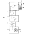
- FIG. 1 is a diagram showing a configuration of a semiconductor device manufacturing apparatus 10.
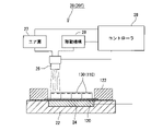
- FIG. 2 is a diagram showing a configuration of a surface treatment device 20 incorporated in the manufacturing device 10.
- This manufacturing device 10 manufactures a semiconductor device by bonding one or more chips 110 to a wafer 100 that functions as a substrate.
- a wafer 100 that functions as a substrate.
- hydrogen bonds are used, which will be described later.
- the manufacturing apparatus 10 includes a chip supply unit 12, a substrate supply unit 14, a bonding unit 16, a first surface treatment device 20f, and a second surface treatment device 20s. ..
- the chip supply unit 12 supplies the chip 110 to the first surface treatment device 20f.
- the chip 110 is supplied to the first surface treatment device 20f in a state of being adhered to the dicing tape 120 (not visible in FIG. 1) stretched inside the dicing ring 122 which is a frame member of the annulus. ..
- the bottom surface of the chip 110 (that is, the joint surface with the wafer 100) is adhered to the dicing tape 120 in an upward posture.
- the substrate supply unit 14 carries in and out the wafer 100, and has, for example, an arm robot (not shown) that conveys the wafer 100.
- the unprocessed wafer 100 is carried in from the carry-in port 14a and is conveyed to the second surface treatment device 20s. Further, the semiconductor device manufactured by bonding is carried out from the carry-out port 14b.
- the first surface treatment device 20f applies a hydrophilization treatment to the surface of the supplied chip 110.
- the second surface treatment device 20s applies a hydrophilization treatment to the surface of the supplied wafer 100.
- the configurations of the first surface treatment device 20f and the second surface treatment device 20s are almost the same. In the following, when the two are not distinguished, it is referred to as "surface treatment device 20". The specific configuration of the surface treatment device 20 will be described later.
- the bonding unit 16 bonds one or more chips 110 to the wafer 100 to manufacture a semiconductor device.
- the bonding unit 16 has a stage on which the wafer 100 is placed, and a bonding head (none of which is shown) capable of sucking and holding the chip 110 and heating the chip 110. The bonding process by the bonding unit 16 will be described with reference to FIG.
- FIG. 3 is an image diagram showing the state of bonding.
- the chip 110 is bonded to the upper surface of the wafer 100.
- another chip 110 is bonded on the chip 110 bonded to the wafer 100.
- Electrodes 102 and 112 are provided on these bonding surfaces, that is, the upper surface of the wafer 100, the bottom surface of the chip 110, and the upper surface of the chip 110.
- the bonding unit 16 bonds the electrode 112 of the chip 110 and the electrode 112 of the wafer 100 or the electrode 112 of another chip 110 so that they are in contact with each other. As a result, the wafer 100 and the chip 110, or the chip 110 and the chip 110 are electrically connected.
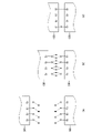
- FIG. 4 is an image diagram showing a state of hydrogen bonding.
- reference numeral 130 is an object to be joined to each other, that is, a chip 110 or a wafer 100.
- the wafer 100 or another chip 110 is bonded to the object 130, and when the wafer 100 is the object 130, the chip 110 is bonded to the object 130. It becomes an object to be joined.
- the joint surface of the object 130 is hydrophilized in advance by the surface treatment device 20. The specific method of the hydrophilization treatment will be described later, but by performing the hydrophilization treatment, as shown in FIG.
- the Si atom and the OH group on the bonding surface of the object 130 are chemically bonded.
- An OH group adheres to the joint surface of the object 130.
- an OH group attached to one object 130 and an OH group attached to the other object 130 are in a state of being molecularly bonded to each other, that is, a state of being hydrogen-bonded.
- the hydrogen bond has a certain degree of bonding force, it has not reached a sufficient bonding force as a semiconductor device. Therefore, after the objects 130 are hydrogen-bonded to each other, the objects 130 are heated in order to further increase the bonding force.
- the object 130 is heated after hydrogen bonding, the water molecule H2O evaporates, and as shown in FIG. 4 (c), the Si atoms of each of the two objects 130 are in a state of being bonded to each other. In this state, the two objects 130 are directly bonded atomically, so that a very strong bonding force can be obtained.
- a hydrophilization treatment to attach an OH group to the bonding surface of the object 130.
- a first surface treatment device 20f and a second surface treatment device 20s are provided for the hydrophilization treatment. Since the configurations of the first surface treatment apparatus 20f and the second surface treatment apparatus 20s are substantially the same, the configuration of the surface treatment apparatus 20 will be described below by taking the first surface treatment apparatus 20f as an example.
- FIG. 2 is a diagram showing the configuration of the surface treatment device 20 (specifically, the first surface treatment device 20f).
- the surface treatment device 20 temporarily causes dew condensation on the joint surface of the object 130 to make the joint surface hydrophilic.
- the surface treatment device 20 includes a support base 22 that supports the object 130, and a spray nozzle 26 that blows humidified air onto the object 130.
- the support base 22 is a table on which the object 130 is placed with the joint surface of the object 130 exposed to the outside so as to support the surface opposite to the joint surface of the object.
- the chip 110 which is the object 130
- the support base 22 incorporates a cooler 24 for cooling the object 130.
- the cooler 24 includes, for example, a cooling plate and a cooling mechanism for cooling the cooling plate.
- the cooling plate is a plate on which the object 130 is placed, and is made of a metal having high heat transfer properties, for example, copper or aluminum.
- a heat absorbing element such as a Pelche element, a heat pump, or the like can be used.
- the drive of such a cooling mechanism is controlled by the controller 28.
- the controller 28 controls the drive of the manufacturing apparatus 10, and is, for example, a computer having a processor and a memory.
- the cooler 24 covers all of one or more objects 130, while the frame member (ie, dicing ring 122) surrounding one or more objects 130 is set to a position and size that does not cover. ing.
- the frame member ie, dicing ring 122
- the occurrence of dew condensation on the surface of the frame member can be prevented, which will be described later.
- a spray nozzle 26 is provided above the support base 22.
- the spray nozzle 26 is a nozzle that blows humidified air onto the joint surface of the object 130.
- An air source 27 that generates humidified air and supplies it to the spray nozzle 26 is connected to the spray nozzle 26.
- the air source 27 uses sufficiently purified clean air and pure water to generate humidified air having a predetermined temperature and humidity.
- a pump for pumping the supplied humidified air, a valve for controlling the discharge of the humidified air (neither of them is shown), and the like are provided. May be good. Further, in this example, the spraying area of the spray nozzle 26 cannot cover all of one or more objects 130 supported by the support base 22.
- a moving mechanism 29 for moving the spray nozzle 26 with respect to the support base 22 is provided.
- the moving mechanism 29 for example, an XY table or the like using a motor as a drive source can be used.
- the spray nozzle 26 can scan the joint surfaces of all one or more objects 130.
- the blowing of humidified air by the blowing nozzle 26 is driven and controlled by the controller 28.
- the conditions of the humidified air when the object 130 is not cooled by the cooler 24 will be examined.
- the temperature of the joint surface of the object 130 becomes the same as the temperature Ta of the surrounding atmosphere.
- the saturated water vapor pressure at this temperature Ta is Ha. If air having a water vapor pressure exceeding the saturated water vapor pressure Ha comes into contact with the joint surface, dew condensation will occur on the joint surface. Therefore, the humidified air may have a water vapor pressure equal to or higher than the saturated water vapor pressure Ha at the ambient temperature Ta (that is, the temperature of the joint surface).
- the humidity of the surrounding atmosphere is sufficiently low, and the dew condensation evaporates.
- OH groups remain attached to the surface of the joint surface even if the droplets evaporate thereafter. In other words, according to the method, an appropriate amount of OH groups can be easily attached to the joint surface, while the residual droplets can be effectively prevented.
- the object 130 may be cooled by the cooler 24 in conjunction with the blowing of the humidified air.
- the conditions of the humidified air when the object 130 is cooled by the cooler 24 will be described with reference to FIG.
- the object 130 When cooling the object 130, it is necessary to suppress the cooling temperature to a temperature at which dew condensation does not occur in the surrounding atmosphere. Specifically, when the temperature of the surrounding atmosphere is Ta and the humidity is Aa%, the water vapor pressure contained in the surrounding atmosphere is Hc. Since the dew point of the water vapor pressure Hc is Tc, dew condensation occurs in the surrounding atmosphere at a temperature of Tc or less. Therefore, when cooling the object 130, the joint surface temperature must exceed the dew point of the water vapor pressure contained in the surrounding atmosphere, or Tc in the example of FIG.
- the surface temperature of the frame member is the same as the temperature Ta of the surrounding atmosphere.
- the humidity difference may be utilized to cause dew condensation only on the joint surface of the cooled object 130 and not to cause dew condensation on the surface of the uncooled frame member.
- the humidified air may contain a water vapor pressure of not less than the saturated water vapor pressure Hc of the joint surface temperature Td and less than the saturated water vapor pressure Ha of the ambient temperature Ta.
- the humidity of the humidified air is set to Ac% or more and less than Ab%, dew condensation occurs on the joint surface, and dew condensation on the frame member can be prevented.
- the joint surface hydrophilic by cooling the object 130 until dew condensation occurs. That is, in the example of FIG. 7, if the joint surface of the object 130 is cooled to the dew point temperature Tc or less of the water vapor pressure Hc in the surrounding atmosphere, dew condensation occurs on the joint surface without blowing humidified air. However, it takes some time to raise the once cooled object 130 to a temperature at which dew condensation evaporates. Therefore, when the object 130 is cooled to cause dew condensation, the dew condensation continues until the object 130 rises to a temperature at which the object 130 can evaporate, and a large amount of droplets are generated on the joint surface.
- the spray nozzle 26 since the spraying area of the spray nozzle 26 is smaller than the total area of the plurality of objects 130 mounted on the support base 22, the spray nozzle 26 is moved and scanned.
- the configuration of such a spray nozzle 26 may be changed as appropriate.
- the spray nozzle 26 may have a spray area that can cover all of the plurality of objects 130.
- a plurality of spray holes 26a provided in the spray nozzle 26 may be provided. With such a configuration, humidified air can be more reliably and evenly dispersed.
- the spray hole 26a provided in the spray nozzle 26 may be a single spray hole 26a as shown in FIG. 9B.
- the configuration of the spray nozzle 26 can be simplified. Further, the humidified air may be blown in a columnar shape as shown in FIG. 9 (b), or may be blown in a conical shape as the diameter increases as it goes downstream, as shown in FIG. 9 (c).
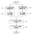
- the chip 110 is conveyed from the chip supply unit 12 to the first surface treatment device 20f (S10).
- the chip 110 is carried into the first surface treatment device 20f in a state of being adhered to the dicing tape 120 stretched inside the dicing ring 122.
- a hydrophilic treatment is applied to the joint surfaces of one or more chips 110 (S12). Specifically, in a state where the chip 110 is placed on the support base 22, the chip 110 is cooled and humidified air is blown to the joint surface of the chip 110 by the spray nozzle 26.
- the hydrophilic treatment of the wafer 100 is also performed. That is, the wafer 100 that functions as a substrate is conveyed from the substrate supply unit 14 to the second surface treatment device 20s (S14). Subsequently, the transferred wafer 100 is subjected to a hydrophilization treatment (S16). Specifically, in a state where the wafer 100 is placed on the support base 22, the wafer 100 is cooled and humidified air is blown to the joint surface of the wafer 100 by the spray nozzle 26.
- the chip 110 is temporarily bonded to the wafer 100 by hydrogen bonding (S18).
- the hydrophilized wafer 100 is conveyed to the bonding unit 16 and placed on a table provided in the bonding unit 16. Further, the bonding tool provided in the bonding unit 16 sucks and holds the hydrophilized chip 110 and places it on the upper surface of the wafer 100.
- the bonding surfaces of the chip 110 and the wafer 100 come into contact with each other, the OH groups attached to both bonding surfaces form hydrogen bonds. As a result, the chip 110 and the wafer 100 are temporarily joined with a certain degree of joining force.
- the temporarily bonded wafer 100 and the chip 110 are subsequently heated, and the two are finally bonded (S20).
- S20 By heating the chip 110 and the wafer 100, water molecules at the bonding interface evaporate, and the Si atoms of both are firmly bonded to each other. So to speak, the silicon of the chip 110 and the silicon of the wafer 100 are atomically bonded. This provides a strong bond.
- the production of the semiconductor device is completed.
- the chips 110 are not laminated
- two or more chips 110 may be laminated in the thickness direction.
- the upper surface of the chip 110 located on the lower side serves as a joining surface with other chips 110 laminated on the upper side thereof, but the upper surface of the lower chip 110 may be hydrophilized. It does not have to be.
- the upper surface of the lower chip 110 is hydrophilized, for example, after the lower chip 110 is placed on the wafer 100, the lower chip 110 is placed on the surface treatment device 20 again together with the wafer 100. , Just put it in.
- the configuration described so far is an example, in which the surface treatment device 20 has at least a support base 22 that supports a surface of the object 130 on the side opposite to the joint surface, and the joint surface at the temperature of the joint surface.
- Other configurations may be appropriately modified as long as it has a spray nozzle for blowing humidified air having a water vapor pressure equal to or higher than the corresponding saturated water vapor pressure.
- both the chip 110 and the wafer 100 are hydrophilized, but the hydrophilization treatment may be applied only to at least one of the chip 110 and the wafer 100. Therefore, the manufacturing apparatus 10 may have only one of the first surface treatment apparatus 20f and the second surface treatment apparatus 20s, and may not have the other. Further, in this example, the object 130 is cooled in the hydrophilization treatment, but the object 130 does not have to be cooled.
- the hydrophilization treatment is performed on the joint surface, but prior to the hydrophilization treatment, another surface treatment, for example, irradiating the joint surface with plasma to activate the atoms on the joint surface.
- Plasma treatment may be performed.
- the surface treatment device 20 is incorporated in the manufacturing device 10 of the semiconductor device, but the surface treatment device 20 may be incorporated in another device for joining the object 130 by utilizing hydrogen bonds. .. Further, the surface treatment device 20 may be used alone without being incorporated in another device.
Landscapes
- Pressure Welding/Diffusion-Bonding (AREA)
- Container, Conveyance, Adherence, Positioning, Of Wafer (AREA)
- Die Bonding (AREA)
- Wire Bonding (AREA)
Abstract
Description
Claims (7)
- 被接合物に水素結合を利用して接合される対象物の接合面に、前記接合に先立って、親水化処理を施す表面処理装置であって、
1以上の前記対象物の接合面と反対の面を支持する支持ベースと、
前記支持ベースで支持された前記対象物の接合面に、前記接合面の温度に対応する飽和水蒸気圧以上の水蒸気圧を有した加湿空気を吹き付けることで、前記接合面に結露を一時的に発生させる吹付ノズルと、
を備えることを特徴とする表面処理装置。 - 請求項1に記載の表面処理装置であって、さらに、
前記支持ベースは、前記接合面の温度を、周辺雰囲気の温度より低く、かつ、前記周辺雰囲気の水蒸気圧の露点温度よりも高い温度に、冷却する冷却器を備える、ことを特徴とする表面処理装置。 - 請求項2に記載の表面処理装置であって、
1以上の前記対象物は、その周囲を枠部材によって取り囲まれた状態で前記支持ベースに載置され、
前記冷却器は、1以上の前記対象物を冷却し、前記枠部材は冷却しない、位置およびサイズである、
ことを特徴とする表面処理装置。 - 請求項1から3のいずれか一項に記載の表面処理装置であって、
前記吹付ノズルは、前記加湿空気の吹き付けと並行して、前記支持ベースに対して移動可能である、ことを特徴とする表面処理装置。 - 請求項1から3のいずれか一項に記載の表面処理装置であって、
前記吹付ノズルは、1以上の前記対象物全てをカバーする吹き付け面積を有する、ことを特徴とする表面処理装置。 - 請求項1から5のいずれか一項に記載の表面処理装置であって、
前記対象物は、半導体集積回路であるチップまたは当該チップが接合されるウエハである、ことを特徴とする表面処理装置。 - ウエハに半導体集積回路であるチップを、水素結合を利用して接合することで半導体装置を製造する半導体装置の製造装置であって、
前記チップを、前記ウエハまたは前記ウエハに実装された他のチップの上面に接合するボンディングユニットと、
前記接合に先立って、前記チップまたは前記ウエハである対象物の接合面に親水化処理を施す1以上の表面処理装置と、
を備え、前記表面処理装置は、
1以上の前記対象物の接合面と反対の面を支持する支持ベースと、
前記支持ベースで支持された前記対象物の接合面に、前記接合面の温度に対応する飽和水蒸気圧以上の水蒸気圧を有した加湿空気を吹き付けることで、前記接合面に結露を一時的に発生させる吹付ノズルと、
を備えることを特徴とする半導体装置の製造装置。
Priority Applications (6)
| Application Number | Priority Date | Filing Date | Title |
|---|---|---|---|
| US18/029,663 US12489004B2 (en) | 2020-10-05 | 2020-10-05 | Surface treatment apparatus and manufacturing apparatus for semiconductor device |
| EP20956668.6A EP4227980A4 (en) | 2020-10-05 | 2020-10-05 | SURFACE TREATMENT DEVICE AND SEMICONDUCTOR DEVICE MANUFACTURING APPARATUS |
| CN202080105720.8A CN116325100A (zh) | 2020-10-05 | 2020-10-05 | 表面处理装置及半导体装置的制造装置 |
| JP2022554990A JP7470457B2 (ja) | 2020-10-05 | 2020-10-05 | 表面処理装置および半導体装置の製造装置 |
| PCT/JP2020/037776 WO2022074719A1 (ja) | 2020-10-05 | 2020-10-05 | 表面処理装置および半導体装置の製造装置 |
| KR1020237010403A KR102894616B1 (ko) | 2020-10-05 | 2020-10-05 | 표면 처리 장치 및 반도체 장치의 제조장치 |
Applications Claiming Priority (1)
| Application Number | Priority Date | Filing Date | Title |
|---|---|---|---|
| PCT/JP2020/037776 WO2022074719A1 (ja) | 2020-10-05 | 2020-10-05 | 表面処理装置および半導体装置の製造装置 |
Publications (1)
| Publication Number | Publication Date |
|---|---|
| WO2022074719A1 true WO2022074719A1 (ja) | 2022-04-14 |
Family
ID=81126739
Family Applications (1)
| Application Number | Title | Priority Date | Filing Date |
|---|---|---|---|
| PCT/JP2020/037776 Ceased WO2022074719A1 (ja) | 2020-10-05 | 2020-10-05 | 表面処理装置および半導体装置の製造装置 |
Country Status (6)
| Country | Link |
|---|---|
| US (1) | US12489004B2 (ja) |
| EP (1) | EP4227980A4 (ja) |
| JP (1) | JP7470457B2 (ja) |
| KR (1) | KR102894616B1 (ja) |
| CN (1) | CN116325100A (ja) |
| WO (1) | WO2022074719A1 (ja) |
Cited By (3)
| Publication number | Priority date | Publication date | Assignee | Title |
|---|---|---|---|---|
| WO2024147278A1 (ja) * | 2023-01-06 | 2024-07-11 | ヤマハロボティクスホールディングス株式会社 | 半導体チップのアライメント方法、接合方法、半導体装置、並びに電子部品製造システム |
| WO2024224899A1 (ja) * | 2023-04-24 | 2024-10-31 | ヤマハロボティクスホールディングス株式会社 | プラズマ処理方法及び接合システム |
| JP2026501395A (ja) * | 2022-12-28 | 2026-01-14 | コミッサリア ア レネルジー アトミーク エ オ ゼネルジ ザルタナテイヴ | ダイツーウエハー直接ハイブリッド接合方法 |
Families Citing this family (1)
| Publication number | Priority date | Publication date | Assignee | Title |
|---|---|---|---|---|
| JP2022150172A (ja) * | 2021-03-26 | 2022-10-07 | 株式会社ディスコ | ウエーハの貼り合わせ方法 |
Citations (5)
| Publication number | Priority date | Publication date | Assignee | Title |
|---|---|---|---|---|
| JP2012175043A (ja) | 2011-02-24 | 2012-09-10 | Tokyo Electron Ltd | 接合装置、接合システム、接合方法、プログラム及びコンピュータ記憶媒体 |
| JP2015211130A (ja) * | 2014-04-25 | 2015-11-24 | ボンドテック株式会社 | 基板接合装置および基板接合方法 |
| WO2017155002A1 (ja) * | 2016-03-11 | 2017-09-14 | ボンドテック株式会社 | 基板接合方法 |
| WO2018062467A1 (ja) * | 2016-09-30 | 2018-04-05 | ボンドテック株式会社 | 基板接合方法および基板接合装置 |
| JP2018201022A (ja) * | 2014-04-25 | 2018-12-20 | 須賀 唯知 | 基板接合装置および基板接合方法 |
Family Cites Families (3)
| Publication number | Priority date | Publication date | Assignee | Title |
|---|---|---|---|---|
| JP2013243333A (ja) * | 2012-04-24 | 2013-12-05 | Tadatomo Suga | チップオンウエハ接合方法及び接合装置並びにチップとウエハとを含む構造体 |
| JP6337400B2 (ja) | 2012-04-24 | 2018-06-06 | 須賀 唯知 | チップオンウエハ接合方法及び接合装置並びにチップとウエハとを含む構造体 |
| US10964664B2 (en) * | 2018-04-20 | 2021-03-30 | Invensas Bonding Technologies, Inc. | DBI to Si bonding for simplified handle wafer |
-
2020
- 2020-10-05 KR KR1020237010403A patent/KR102894616B1/ko active Active
- 2020-10-05 WO PCT/JP2020/037776 patent/WO2022074719A1/ja not_active Ceased
- 2020-10-05 US US18/029,663 patent/US12489004B2/en active Active
- 2020-10-05 CN CN202080105720.8A patent/CN116325100A/zh active Pending
- 2020-10-05 EP EP20956668.6A patent/EP4227980A4/en active Pending
- 2020-10-05 JP JP2022554990A patent/JP7470457B2/ja active Active
Patent Citations (5)
| Publication number | Priority date | Publication date | Assignee | Title |
|---|---|---|---|---|
| JP2012175043A (ja) | 2011-02-24 | 2012-09-10 | Tokyo Electron Ltd | 接合装置、接合システム、接合方法、プログラム及びコンピュータ記憶媒体 |
| JP2015211130A (ja) * | 2014-04-25 | 2015-11-24 | ボンドテック株式会社 | 基板接合装置および基板接合方法 |
| JP2018201022A (ja) * | 2014-04-25 | 2018-12-20 | 須賀 唯知 | 基板接合装置および基板接合方法 |
| WO2017155002A1 (ja) * | 2016-03-11 | 2017-09-14 | ボンドテック株式会社 | 基板接合方法 |
| WO2018062467A1 (ja) * | 2016-09-30 | 2018-04-05 | ボンドテック株式会社 | 基板接合方法および基板接合装置 |
Non-Patent Citations (1)
| Title |
|---|
| See also references of EP4227980A4 |
Cited By (4)
| Publication number | Priority date | Publication date | Assignee | Title |
|---|---|---|---|---|
| JP2026501395A (ja) * | 2022-12-28 | 2026-01-14 | コミッサリア ア レネルジー アトミーク エ オ ゼネルジ ザルタナテイヴ | ダイツーウエハー直接ハイブリッド接合方法 |
| JP7815553B2 (ja) | 2022-12-28 | 2026-02-17 | コミッサリア ア レネルジー アトミーク エ オ ゼネルジ ザルタナテイヴ | ダイツーウエハー直接ハイブリッド接合方法 |
| WO2024147278A1 (ja) * | 2023-01-06 | 2024-07-11 | ヤマハロボティクスホールディングス株式会社 | 半導体チップのアライメント方法、接合方法、半導体装置、並びに電子部品製造システム |
| WO2024224899A1 (ja) * | 2023-04-24 | 2024-10-31 | ヤマハロボティクスホールディングス株式会社 | プラズマ処理方法及び接合システム |
Also Published As
| Publication number | Publication date |
|---|---|
| JP7470457B2 (ja) | 2024-04-18 |
| JPWO2022074719A1 (ja) | 2022-04-14 |
| EP4227980A1 (en) | 2023-08-16 |
| US20230369079A1 (en) | 2023-11-16 |
| EP4227980A4 (en) | 2024-09-25 |
| KR20230054731A (ko) | 2023-04-25 |
| CN116325100A (zh) | 2023-06-23 |
| US12489004B2 (en) | 2025-12-02 |
| KR102894616B1 (ko) | 2025-12-02 |
Similar Documents
| Publication | Publication Date | Title |
|---|---|---|
| WO2022074719A1 (ja) | 表面処理装置および半導体装置の製造装置 | |
| KR20130111533A (ko) | 접합시스템, 기판 처리 시스템, 접합방법, 프로그램 및 컴퓨터 저장매체 | |
| KR20240038027A (ko) | 처리 방법 및 플라즈마 처리 장치 | |
| JP7612428B2 (ja) | ダイボンディング装置、剥離治具および半導体装置の製造方法 | |
| KR20220048018A (ko) | 접합 장치, 접합 시스템 및 접합 방법 | |
| KR20160086277A (ko) | 접합 장치, 접합 시스템, 접합 방법 및 컴퓨터 기억 매체 | |
| JP2019204832A (ja) | 部品実装システム、基板接合システム、部品実装方法および基板接合方法 | |
| JPWO2022074719A5 (ja) | ||
| TW200525599A (en) | Attaching apparatus and method | |
| US8187923B2 (en) | Laser release process for very thin Si-carrier build | |
| US20190051618A1 (en) | Laminating device and method for fabricating semiconductor package using the same | |
| CN113436988A (zh) | 芯片贴装装置、剥离夹具以及半导体器件的制造方法 | |
| JP2016207786A (ja) | 半導体装置の製造装置及び製造方法 | |
| JP6055387B2 (ja) | 接合方法、プログラム、コンピュータ記憶媒体及び接合システム | |
| TWI799989B (zh) | 表面處理裝置及半導體裝置的製造裝置 | |
| JP4046076B2 (ja) | 電子部品搭載装置 | |
| TW201222710A (en) | Substrate holding apparatus and the method thereof | |
| JP2006080100A (ja) | 接合方法および装置 | |
| TWI870271B (zh) | 防止產生氣泡的加熱固晶方法 | |
| WO2026083837A1 (ja) | 処理システム及び処理方法 | |
| US9735033B2 (en) | Multiple swivel arm design in hybrid bonder | |
| WO2026083836A1 (ja) | 接合装置、処理システム及び接合方法 | |
| JPH07283379A (ja) | 基板の貼り合わせ方法 | |
| JP2010045160A (ja) | ダイボンダおよびボンディング方法 | |
| TW202549009A (zh) | 半導體製造裝置 |
Legal Events
| Date | Code | Title | Description |
|---|---|---|---|
| 121 | Ep: the epo has been informed by wipo that ep was designated in this application |
Ref document number: 20956668 Country of ref document: EP Kind code of ref document: A1 |
|
| DPE1 | Request for preliminary examination filed after expiration of 19th month from priority date (pct application filed from 20040101) | ||
| ENP | Entry into the national phase |
Ref document number: 2022554990 Country of ref document: JP Kind code of ref document: A |
|
| ENP | Entry into the national phase |
Ref document number: 20237010403 Country of ref document: KR Kind code of ref document: A |
|
| NENP | Non-entry into the national phase |
Ref country code: DE |
|
| ENP | Entry into the national phase |
Ref document number: 2020956668 Country of ref document: EP Effective date: 20230508 |