WO2022080268A1 - エッチングガス、エッチング方法、及び半導体素子の製造方法 - Google Patents
エッチングガス、エッチング方法、及び半導体素子の製造方法 Download PDFInfo
- Publication number
- WO2022080268A1 WO2022080268A1 PCT/JP2021/037422 JP2021037422W WO2022080268A1 WO 2022080268 A1 WO2022080268 A1 WO 2022080268A1 JP 2021037422 W JP2021037422 W JP 2021037422W WO 2022080268 A1 WO2022080268 A1 WO 2022080268A1
- Authority
- WO
- WIPO (PCT)
- Prior art keywords
- etching
- gas
- etched
- fluorobutene
- silicon
- Prior art date
- Legal status (The legal status is an assumption and is not a legal conclusion. Google has not performed a legal analysis and makes no representation as to the accuracy of the status listed.)
- Ceased
Links
Images

Classifications
-
- C—CHEMISTRY; METALLURGY
- C09—DYES; PAINTS; POLISHES; NATURAL RESINS; ADHESIVES; COMPOSITIONS NOT OTHERWISE PROVIDED FOR; APPLICATIONS OF MATERIALS NOT OTHERWISE PROVIDED FOR
- C09K—MATERIALS FOR MISCELLANEOUS APPLICATIONS, NOT PROVIDED FOR ELSEWHERE
- C09K13/00—Etching, surface-brightening or pickling compositions
-
- H—ELECTRICITY
- H10—SEMICONDUCTOR DEVICES; ELECTRIC SOLID-STATE DEVICES NOT OTHERWISE PROVIDED FOR
- H10P—GENERIC PROCESSES OR APPARATUS FOR THE MANUFACTURE OR TREATMENT OF DEVICES COVERED BY CLASS H10
- H10P50/00—Etching of wafers, substrates or parts of devices
- H10P50/20—Dry etching; Plasma etching; Reactive-ion etching
- H10P50/24—Dry etching; Plasma etching; Reactive-ion etching of semiconductor materials
- H10P50/242—Dry etching; Plasma etching; Reactive-ion etching of semiconductor materials of Group IV materials
-
- H—ELECTRICITY
- H10—SEMICONDUCTOR DEVICES; ELECTRIC SOLID-STATE DEVICES NOT OTHERWISE PROVIDED FOR
- H10P—GENERIC PROCESSES OR APPARATUS FOR THE MANUFACTURE OR TREATMENT OF DEVICES COVERED BY CLASS H10
- H10P50/00—Etching of wafers, substrates or parts of devices
- H10P50/20—Dry etching; Plasma etching; Reactive-ion etching
- H10P50/26—Dry etching; Plasma etching; Reactive-ion etching of conductive or resistive materials
- H10P50/264—Dry etching; Plasma etching; Reactive-ion etching of conductive or resistive materials by chemical means
- H10P50/266—Dry etching; Plasma etching; Reactive-ion etching of conductive or resistive materials by chemical means by vapour etching only
-
- H—ELECTRICITY
- H10—SEMICONDUCTOR DEVICES; ELECTRIC SOLID-STATE DEVICES NOT OTHERWISE PROVIDED FOR
- H10P—GENERIC PROCESSES OR APPARATUS FOR THE MANUFACTURE OR TREATMENT OF DEVICES COVERED BY CLASS H10
- H10P50/00—Etching of wafers, substrates or parts of devices
- H10P50/20—Dry etching; Plasma etching; Reactive-ion etching
- H10P50/28—Dry etching; Plasma etching; Reactive-ion etching of insulating materials
- H10P50/282—Dry etching; Plasma etching; Reactive-ion etching of insulating materials of inorganic materials
- H10P50/283—Dry etching; Plasma etching; Reactive-ion etching of insulating materials of inorganic materials by chemical means
-
- H—ELECTRICITY
- H10—SEMICONDUCTOR DEVICES; ELECTRIC SOLID-STATE DEVICES NOT OTHERWISE PROVIDED FOR
- H10P—GENERIC PROCESSES OR APPARATUS FOR THE MANUFACTURE OR TREATMENT OF DEVICES COVERED BY CLASS H10
- H10P50/00—Etching of wafers, substrates or parts of devices
- H10P50/20—Dry etching; Plasma etching; Reactive-ion etching
- H10P50/26—Dry etching; Plasma etching; Reactive-ion etching of conductive or resistive materials
- H10P50/264—Dry etching; Plasma etching; Reactive-ion etching of conductive or resistive materials by chemical means
- H10P50/266—Dry etching; Plasma etching; Reactive-ion etching of conductive or resistive materials by chemical means by vapour etching only
- H10P50/267—Dry etching; Plasma etching; Reactive-ion etching of conductive or resistive materials by chemical means by vapour etching only using plasmas
Definitions
- the etching of the present embodiment can be achieved by either plasma etching using plasma or plasmaless etching using plasma.
- plasma etching include reactive ion etching (RIE), inductively coupled plasma (ICP) etching, capacitively coupled plasma (CCP: Capacitive Coupled Plasma) etching, and electron etching.
- RIE reactive ion etching
- ICP inductively coupled plasma
- CCP capacitively coupled plasma
- electron etching Electron Cyclotron Resonance
- Plasma etching microwave plasma etching can be mentioned.
- those having a boiling point at 1 atm of 50 ° C. or lower are preferable, and those having a boiling point of 40 ° C. or lower are more preferable.
- the boiling point at 1 atm is within the above range, when the fluorobutene gas is introduced into, for example, a plasma etching apparatus, the fluorobutene gas is difficult to liquefy inside a pipe or the like into which the fluorobutene gas is introduced. Therefore, it is possible to suppress the occurrence of troubles caused by the liquefaction of the fluorobutene gas, so that the plasma etching process can be efficiently performed.
- the etching gas is a gas containing the above-mentioned fluorobutene.
- the etching gas may be a gas consisting only of the above-mentioned fluorobutene or a mixed gas containing the above-mentioned fluorobutene and a diluting gas. Further, it may be a mixed gas containing the above-mentioned fluorobutene, a diluting gas and an added gas.
- the diluting gas at least one selected from nitrogen gas (N 2 ), helium (He), neon (Ne), argon (Ar), krypton (Kr), and xenon (Xe) can be used.
- an oxidizing gas for example, an oxidizing gas, a fluorocarbon gas, or a hydrofluorocarbon gas
- the oxidizing gas include oxygen gas (O 2 ), ozone (O 3 ), carbon monoxide (CO), carbon dioxide (CO 2 ), nitric oxide (NO), and nitrous oxide (N 2 ). O) and nitrogen dioxide (NO 2 ) can be mentioned.
- fluorocarbons include carbon tetrafluoride (CF 4 ), hexafluoromethane (C 2 F 6 ), and octafluoropropane (C 3 F 8 ).
- the sum of the concentrations of copper, zinc, manganese, cobalt and silicon may be 1 mass ppb or more.
- concentration of metal impurities such as copper, zinc, manganese, cobalt and silicon in the etching gas can be quantified by an inductively coupled plasma mass spectrometer (ICP-MS).
- the etching selectivity tends to be high.
- the etching selection ratio which is the ratio of the etching rate of the object to be etched containing silicon to the etching rate of the non-etched object, tends to be 10 or more.
- the bias power constituting the potential difference between the plasma generated during etching and the member to be etched may be selected from 0 to 10000 W depending on the desired etching shape, and 0 to 1000 W when selectively etching is performed. The degree is preferable. Anisotropic etching can be performed by this potential difference.
- the non-etching target can be used as a resist or a mask for suppressing etching of the etching target by the etching gas. Therefore, in the etching method according to the present embodiment, the patterned non-etched object is used as a resist or a mask to process the etched object into a predetermined shape (for example, the film-shaped etched object of the member to be etched). Since it can be used for a method such as (processing an object to a predetermined film thickness), it can be suitably used for manufacturing a semiconductor element. Further, since the non-etched object is hardly etched, it is possible to suppress the etching of the portion of the semiconductor element that should not be etched, and it is possible to prevent the characteristics of the semiconductor element from being lost by etching. can.
- the non-etching object remaining after patterning can be removed by a removal method generally used in the semiconductor device manufacturing process. For example, ashing with an oxidizing gas such as oxygen plasma or ozone, or dissolution using a chemical solution such as APM (mixed solution of ammonia water and hydrogen peroxide solution), SPM (mixed solution of sulfuric acid and hydrogen peroxide solution) or organic solvent. Removal is mentioned.
- ashing with an oxidizing gas such as oxygen plasma or ozone
- a chemical solution such as APM (mixed solution of ammonia water and hydrogen peroxide solution), SPM (mixed solution of sulfuric acid and hydrogen peroxide solution) or organic solvent. Removal is mentioned.
- the etching apparatus of FIG. 1 is a plasma etching apparatus that performs etching using plasma. First, the etching apparatus of FIG. 1 will be described.
- the type of plasma generation mechanism of the plasma generator is not particularly limited, and may be one in which a high frequency voltage is applied to a parallel plate or one in which a high frequency current is passed through a coil.
- a high frequency voltage is applied to the member 12 to be etched in plasma
- a negative voltage is applied to the member 12 to be etched, and positive ions are incident on the member 12 to be etched at high speed and vertically, so that anisotropic etching is possible.
- the etching apparatus of FIG. 1 is provided with an etching gas supply unit that supplies the etching gas inside the chamber 10.
- This etching gas supply unit is a fluorobutene gas supply unit 1 that connects a fluorobutene gas supply unit 1 that supplies a fluorobutene gas, a dilution gas supply unit 2 that supplies a dilution gas, a fluorobutene gas supply unit 1 and a chamber 10. It has a diluting gas supply pipe 6 for connecting a diluting gas supply unit 2 to an intermediate portion of the fluorobutene gas supply pipe 5 and a diluting gas supply pipe 5.
- nickel-based alloys include Inconel (registered trademark), Hastelloy (registered trademark), Monel (registered trademark) and the like.
- fluororesin include polytetrafluoroethylene (PTFE), polychlorotrifluoroethylene (PCTFE), tetrafluoroethylene / perfluoroalkoxyethylene copolymer (PFA), polyvinylidene fluoride (PVDF), and Teflon.
- PTFE polytetrafluoroethylene
- PCTFE polychlorotrifluoroethylene
- PFA tetrafluoroethylene / perfluoroalkoxyethylene copolymer
- PVDF polyvinylidene fluoride
- Teflon Teflon
- Preparation Example 4 Samples 4-1 to 4-5 were prepared in the same manner as in Preparation Example 1 except that 2,3,3,4,4,4-hexafluoro-1-butene was used as the fluorobutene. .. Then, the concentrations of various metal impurities in each sample were measured by an inductively coupled plasma mass spectrometer. The results are shown in Table 4.
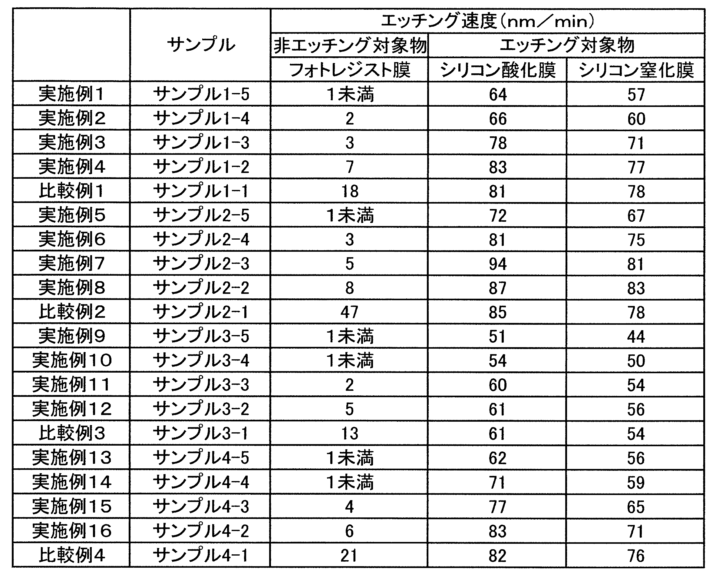
- the test piece was taken out from the chamber, the thicknesses of the silicon oxide film, the silicon nitride film, and the photoresist film were measured, and the amount of decrease in the thickness from each film before etching was calculated.
- the etching rate of each film was calculated by dividing this decrease by the etching time. As a result, the etching rate of the photoresist film was less than 1 nm / min, the etching rate of the silicon oxide film was 64 nm / min, and the etching rate of the silicon nitride film was 57 nm / min. From this result, it was confirmed that the silicon oxide film and the silicon nitride film, which are the objects to be etched, are selectively etched as compared with the photoresist film, which is the object to be etched.
- the etching target is selectively etched as compared with the non-etching target, and the etching is selected. It can be seen that the ratio is 10 or more.
- the etching selectivity of the etching target to the non-etching target is lowered, and the etching is performed. It can be seen that the selection ratio is less than 10.
Landscapes
- Chemical & Material Sciences (AREA)
- Engineering & Computer Science (AREA)
- Materials Engineering (AREA)
- Organic Chemistry (AREA)
- Drying Of Semiconductors (AREA)
- Physics & Mathematics (AREA)
- Plasma & Fusion (AREA)
Abstract
Description
この要求を満たす種々のエッチングガスが提案されており、例えば特許文献1には、ヘキサフルオロイソブテンを含有するエッチングガスが開示されている。ヘキサフルオロイソブテンはエッチング中に反応してポリマー化し、このポリマーの膜でマスクが被覆され保護されるため、高いエッチング選択性が得られやすい。
本発明は、エッチングガスによるエッチングの対象であるエッチング対象物とエッチングガスによるエッチングの対象ではない非エッチング対象物とを有する被エッチング部材にエッチングガスを接触させてエッチングを行った場合に、非エッチング対象物に比べてエッチング対象物を選択的にエッチングすることができるエッチングガス、エッチング方法、及び半導体素子の製造方法を提供することを課題とする。
[1] 一般式C4HxFyで表され且つ前記一般式中のxが1以上7以下、yが1以上7以下、x+yが8であるフルオロブテンを含有するエッチングガスであって、
銅、亜鉛、マンガン、コバルト、及びケイ素のうち少なくとも一種を金属不純物として含有するか又は含有せず、前記含有する場合の銅、亜鉛、マンガン、コバルト、及びケイ素の濃度の和が5000質量ppb以下であるエッチングガス。
[4] 前記フルオロブテンが1,1,1,4,4,4-ヘキサフルオロ-2-ブテン、1,1,1,2,4,4,4-ヘプタフルオロ-2-ブテン、3,3,4,4,4-ペンタフルオロ-1-ブテン、及び2,3,3,4,4,4-ヘキサフルオロ-1-ブテンから選ばれる少なくとも1つである[1]~[3]のいずれか一項に記載のエッチングガス。
[6] 前記エッチングガスが含有する銅、亜鉛、マンガン、コバルト、及びケイ素の濃度の和を5000質量ppb以下とする金属不純物除去工程を、前記エッチング工程の前に備える[5]に記載のエッチング方法。
[8] 前記希釈ガスが、窒素ガス、ヘリウム、アルゴン、ネオン、クリプトン、及びキセノンから選ばれる少なくとも一種である[7]に記載のエッチング方法。
前記被エッチング部材が、前記エッチング対象物及び前記非エッチング対象物を有する半導体基板であり、
前記半導体基板から前記エッチング対象物の少なくとも一部を前記エッチングにより除去する処理工程を備える半導体素子の製造方法。
〔エッチング方法〕
本実施形態のエッチングは、プラズマを用いるプラズマエッチング、プラズマを用いないプラズマレスエッチングのいずれによっても達成できる。プラズマエッチングとしては、例えば、反応性イオンエッチング(RIE:Reactive Ion Etching)、誘導結合型プラズマ(ICP:Inductively Coupled Plasma)エッチング、容量結合型プラズマ(CCP:Capacitively Coupled Plasma)エッチング、電子サイクロトロン共鳴(ECR:Electron Cyclotron Resonance)プラズマエッチング、マイクロ波プラズマエッチングが挙げられる。
本実施形態に係るエッチングガスに含有されるフルオロブテンは、一般式C4HxFyで表されるものであり、且つ、一般式中のxが1以上7以下、yが1以上7以下、x+yが8との3つの条件を満たすものである。フルオロブテンの種類は、上記要件を満たしていれば特に限定されるものではなく、直鎖状のフルオロブテンでも分岐鎖状のフルオロブテン(イソブテン)でも使用可能であるが、フルオロ-1-ブテンに類するものとフルオロ-2-ブテンに類するものが好ましく使用可能である。
上記の観点から、フルオロブテンとしては、例えば、1,1,1,4,4,4-ヘキサフルオロ-2-ブテン(沸点9℃)、1,1,1,2,4,4,4-ヘプタフルオロ-2-ブテン(沸点8℃)、3,3,4,4,4-ペンタフルオロ-1-ブテン(沸点3-6℃)、及び2,3,3,4,4,4-ヘキサフルオロ-1-ブテン(沸点3-7℃)から選ばれる少なくとも1つが好ましい。
エッチングガスは、上記のフルオロブテンを含有するガスである。エッチングガスは、上記のフルオロブテンのみからなるガスであってもよいし、上記のフルオロブテンと希釈ガスを含有する混合ガスであってもよい。また、上記のフルオロブテンと希釈ガスと添加ガスを含有する混合ガスであってもよい。
希釈ガスとしては、窒素ガス(N2)、ヘリウム(He)、ネオン(Ne)、アルゴン(Ar)、クリプトン(Kr)、及びキセノン(Xe)から選ばれる少なくとも一種を用いることができる。
エッチングガス中のフルオロブテンの含有量は、エッチング速度を向上させる観点から、エッチングガスの総量に対して5体積%以上が好ましく、10体積%以上がさらに好ましい。また、フルオロブテンの使用量を抑制する観点から、エッチングガスの総量に対して90体積%以下が好ましく、80体積%以下がさらに好ましい。
本実施形態に係るエッチングガスは、銅、亜鉛、マンガン、コバルト、及びケイ素のうち少なくとも一種を金属不純物として含有するか又は含有しないが、前記含有する場合の銅、亜鉛、マンガン、コバルト、及びケイ素の濃度の和が5000質量ppb以下と低濃度であるため、前述したように上記フルオロブテンの炭素-炭素二重結合の解離が生じにくく、その結果、非エッチング対象物に比べてエッチング対象物を選択的にエッチングすることができる。ここで、前記含有しないとは、誘導結合プラズマ質量分析計(ICP-MS)で定量することができない場合を意味する。
エッチングガス中の銅、亜鉛、マンガン、コバルト、ケイ素等の金属不純物の濃度は、誘導結合プラズマ質量分析計(ICP-MS)で定量することができる。
なお、銅、亜鉛、マンガン、コバルト及びケイ素、並びに、アルカリ金属及びアルカリ土類金属の濃度の総和は、2質量ppb以上であってもよい。
上記フルオロブテンから上記金属不純物を除去する方法(金属不純物除去工程において採用される不純物除去方法)としては、例えば、上記フルオロブテンをフィルターに通過させる方法、吸着剤を接触させる方法、蒸留で分離する方法等がある。そして、具体的には、例えば、ステンレス製シリンダーに上記フルオロブテンを封入し、0℃程度に保持した状態で、後述の実施例に記載の方法によって気相部を抜き出すことで、上記金属不純物の濃度が低下したフルオロブテンを得ることができる。このような金属不純物除去工程によって、エッチングガスが含有するアルカリ金属及びアルカリ土類金属の濃度の和を5000質量ppb以下とした後に、後述のエッチング工程を行うことが好ましい。
本実施形態に係るエッチング方法におけるエッチング工程の圧力条件は特に限定されるものではないが、10Pa以下とすることが好ましく、5Pa以下とすることがより好ましい。圧力条件が上記の範囲内であれば、プラズマを安定して発生させやすい。一方、エッチング工程の圧力条件は0.05Pa以上であることが好ましい。圧力条件が上記の範囲内であれば、電離イオンが多く発生し十分なプラズマ密度が得られやすい。
エッチングガスの流量は、チャンバーの大きさやチャンバー内を減圧する排気設備の能力に応じて、チャンバー内の圧力が一定に保たれるように適宜設定すればよい。
本実施形態に係るエッチング方法におけるエッチング工程の温度条件は特に限定されるものではないが、高いエッチング選択性を得るためには200℃以下とすることが好ましく、マスク等の非エッチング対象物がエッチングされることをより抑制するためには150℃以下とすることがより好ましく、異方性エッチングを行うためには100℃以下とすることがさらに好ましい。ここで、温度条件の温度とは、被エッチング部材の温度であるが、エッチング装置のチャンバー内に設置された、被エッチング部材を支持するステージの温度を使用することもできる。
エッチングを行う際に発生させるプラズマと被エッチング部材との間の電位差を構成するバイアスパワーについては、所望するエッチング形状により0~10000Wから選択すればよく、選択的にエッチングを行う場合は0~1000W程度が好ましい。この電位差によって、異方性エッチングを行うことができる。
本実施形態に係るエッチング方法によりエッチングする被エッチング部材は、エッチング対象物と非エッチング対象物を有するが、エッチング対象物で形成されている部分と非エッチング対象物で形成されている部分とを有する部材でもよいし、エッチング対象物と非エッチング対象物の混合物で形成されている部材でもよい。また、被エッチング部材は、エッチング対象物、非エッチング対象物以外のものを有していてもよい。
また、被エッチング部材の形状は特に限定されるものではなく、例えば、板状、箔状、膜状、粉末状、塊状であってもよい。被エッチング部材の例としては、前述した半導体基板が挙げられる。
エッチング対象物は、ケイ素を含有する材料のみで形成されているものであってもよいし、ケイ素を含有する材料のみで形成されている部分と他の材質で形成されている部分とを有するものであってもよいし、ケイ素を含有する材料と他の材質の混合物で形成されているものであってもよい。ケイ素を含有する材料としては、例えば、酸化ケイ素、窒化ケイ素、ポリシリコン、シリコンゲルマニウム(SiGe)が挙げられる。
また、エッチング対象物の形状は、特に限定されるものではなく、例えば、板状、箔状、膜状、粉末状、塊状であってもよい。
非エッチング対象物は、上記のフルオロブテンと実質的に反応しないか、又は、上記のフルオロブテンとの反応が極めて遅いため、本実施形態に係るエッチング方法によりエッチングを行っても、エッチングがほとんど進行しないものである。非エッチング対象物は、上記のような性質を有するならば特に限定されるものではないが、例えば、フォトレジスト、アモルファスカーボン、窒化チタンや、銅、ニッケル、コバルト等の金属や、これら金属の酸化物、窒化物が挙げられる。これらの中でも、取扱性及び入手容易性の観点から、フォトレジスト、アモルファスカーボンがより好ましい。
エッチングガスをチャンバー10へ供給する際には、エッチングガスの温度を所定値に保持しつつ供給することが好ましい。すなわち、エッチングガスの供給温度は、0℃以上150℃以下であることが好ましい。
例えば、フルオロブテンガス供給用配管5と被エッチング部材12との位置関係は、エッチングガスを被エッチング部材12に接触させることができるならば、特に限定されない。また、チャンバー10の温度調節機構の構成についても、被エッチング部材12の温度を任意の温度に調節できればよいので、ステージ11上に温度調節機構を直接備える構成でもよいし、外付けの温度調節器でチャンバー10の外側からチャンバー10に加温又は冷却を行ってもよい。
(調製例1)
マンガン鋼製の容量1Lのシリンダーを5個用意した。それらシリンダーを順に、シリンダーA、シリンダーB、シリンダーC、シリンダーD、シリンダーEと呼ぶ。シリンダーAには1,1,1,4,4,4-ヘキサフルオロ-2-ブテン(沸点:9℃)500gを充填し、0℃に冷却することにより液化させ、ほぼ100kPaの状態で液相部と気相部とを形成させた。シリンダーB、C、D、Eは、真空ポンプで内部を1kPa以下に減圧した後に-78℃に冷却した。

フルオロブテンとして1,1,1,2,4,4,4-ヘプタフルオロ-2-ブテンを使用した点以外は、調製例1と同様の操作を行って、サンプル2-1~2-5を調製した。そして、それぞれのサンプルの各種金属不純物の濃度を誘導結合プラズマ質量分析計で測定した。結果を表2に示す。

フルオロブテンとして3,3,4,4,4-ペンタフルオロ-1-ブテンを使用した点以外は、調製例1と同様の操作を行って、サンプル3-1~3-5を調製した。そして、それぞれのサンプルの各種金属不純物の濃度を誘導結合プラズマ質量分析計で測定した。結果を表3に示す。
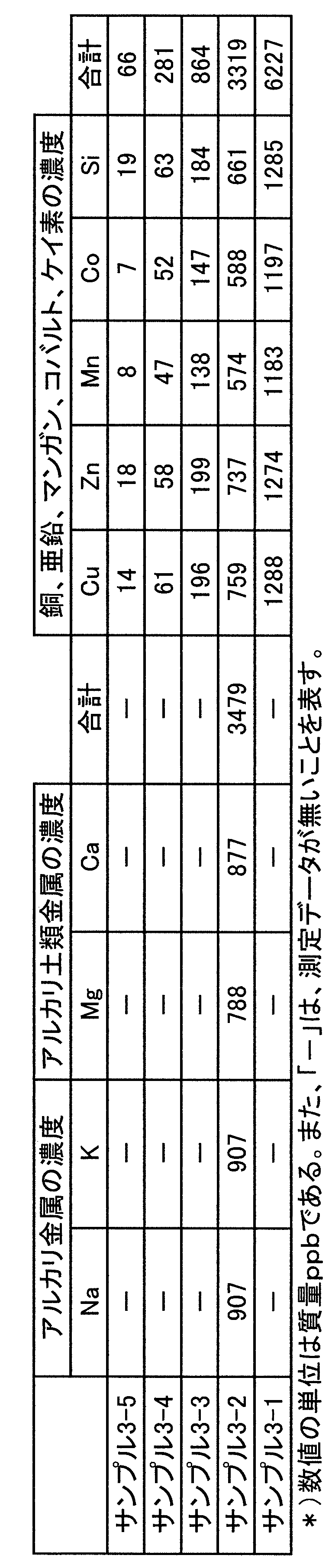
フルオロブテンとして2,3,3,4,4,4-ヘキサフルオロ-1-ブテンを使用した点以外は、調製例1と同様の操作を行って、サンプル4-1~4-5を調製した。そして、それぞれのサンプルの各種金属不純物の濃度を誘導結合プラズマ質量分析計で測定した。結果を表4に示す。

半導体ウェハの表面上に、厚さ1000nmのシリコン酸化膜と、厚さ1000nmのシリコン窒化膜と、厚さ1000nmのフォトレジスト膜とを、積層せず、それぞれ表面に露出するように形成して、これを試験体とした。そして、サンプル1-5の1,1,1,4,4,4-ヘキサフルオロ-2-ブテンを用いて、試験体のエッチングを行った。
実施例2~16及び比較例1~4におけるエッチング条件及びエッチング結果を、実施例1との対比で、表5に示す。すなわち、表5に示した条件以外は、実施例1と同等の条件でエッチングを行った。
2・・・希釈ガス供給部
3・・・フルオロブテンガス流量制御装置
4・・・希釈ガス流量制御装置
5・・・フルオロブテンガス供給用配管
6・・・希釈ガス供給用配管
7・・・フルオロブテンガス圧力制御装置
8・・・希釈ガス圧力制御装置
10・・・チャンバー
11・・・ステージ
12・・・被エッチング部材
13・・・排気用配管
14・・・温度計
15・・・真空ポンプ
16・・・圧力計
Claims (9)
- 一般式C4HxFyで表され且つ前記一般式中のxが1以上7以下、yが1以上7以下、x+yが8であるフルオロブテンを含有するエッチングガスであって、
銅、亜鉛、マンガン、コバルト、及びケイ素のうち少なくとも一種を金属不純物として含有するか又は含有せず、前記含有する場合の銅、亜鉛、マンガン、コバルト、及びケイ素の濃度の和が5000質量ppb以下であるエッチングガス。 - アルカリ金属及びアルカリ土類金属のうち少なくとも一種を前記金属不純物としてさらに含有するか又は含有せず、前記含有する場合の銅、亜鉛、マンガン、コバルト、及びケイ素、並びに、アルカリ金属及びアルカリ土類金属の濃度の総和が10000質量ppb以下である請求項1に記載のエッチングガス。
- 前記アルカリ金属がリチウム、ナトリウム、及びカリウムのうち少なくとも一種であり、前記アルカリ土類金属がマグネシウム及びカルシウムの少なくとも一方である請求項2に記載のエッチングガス。
- 前記フルオロブテンが1,1,1,4,4,4-ヘキサフルオロ-2-ブテン、1,1,1,2,4,4,4-ヘプタフルオロ-2-ブテン、3,3,4,4,4-ペンタフルオロ-1-ブテン、及び2,3,3,4,4,4-ヘキサフルオロ-1-ブテンから選ばれる少なくとも1つである請求項1~3のいずれか一項に記載のエッチングガス。
- 請求項1~4のいずれか一項に記載のエッチングガスを、前記エッチングガスによるエッチングの対象であるエッチング対象物と前記エッチングガスによるエッチングの対象ではない非エッチング対象物とを有する被エッチング部材に接触させ、前記非エッチング対象物に比べて前記エッチング対象物を選択的にエッチングするエッチング工程を備え、前記エッチング対象物がケイ素を含有するエッチング方法。
- 前記エッチングガスが含有する銅、亜鉛、マンガン、コバルト、及びケイ素の濃度の和を5000質量ppb以下とする金属不純物除去工程を、前記エッチング工程の前に備える請求項5に記載のエッチング方法。
- 前記エッチングガスが、前記フルオロブテンのみからなるガス、又は、前記フルオロブテンと希釈ガスを含有する混合ガスである請求項5又は請求項6に記載のエッチング方法。
- 前記希釈ガスが、窒素ガス、ヘリウム、アルゴン、ネオン、クリプトン、及びキセノンから選ばれる少なくとも一種である請求項7に記載のエッチング方法。
- 請求項5~8のいずれか一項に記載のエッチング方法を用いて半導体素子を製造する半導体素子の製造方法であって、
前記被エッチング部材が、前記エッチング対象物及び前記非エッチング対象物を有する半導体基板であり、
前記半導体基板から前記エッチング対象物の少なくとも一部を前記エッチングにより除去する処理工程を備える半導体素子の製造方法。
Priority Applications (6)
| Application Number | Priority Date | Filing Date | Title |
|---|---|---|---|
| CN202180070326.XA CN116325089A (zh) | 2020-10-15 | 2021-10-08 | 蚀刻气体、蚀刻方法以及半导体元件的制造方法 |
| IL302057A IL302057A (en) | 2020-10-15 | 2021-10-08 | Etching gas, etching method, and method for producing semiconductor element |
| JP2022556926A JP7786388B2 (ja) | 2020-10-15 | 2021-10-08 | エッチングガス、エッチング方法、及び半導体素子の製造方法 |
| KR1020237011836A KR20230061542A (ko) | 2020-10-15 | 2021-10-08 | 에칭 가스, 에칭 방법, 및 반도체 소자의 제조 방법 |
| EP21880007.6A EP4231332A4 (en) | 2020-10-15 | 2021-10-08 | Etching gas, etching method, and method for producing semiconductor element |
| US18/031,816 US20230386850A1 (en) | 2020-10-15 | 2021-10-08 | Etching gas, etching method, and method for producing semiconductor device |
Applications Claiming Priority (2)
| Application Number | Priority Date | Filing Date | Title |
|---|---|---|---|
| JP2020173915 | 2020-10-15 | ||
| JP2020-173915 | 2021-10-15 |
Publications (1)
| Publication Number | Publication Date |
|---|---|
| WO2022080268A1 true WO2022080268A1 (ja) | 2022-04-21 |
Family
ID=81208185
Family Applications (1)
| Application Number | Title | Priority Date | Filing Date |
|---|---|---|---|
| PCT/JP2021/037422 Ceased WO2022080268A1 (ja) | 2020-10-15 | 2021-10-08 | エッチングガス、エッチング方法、及び半導体素子の製造方法 |
Country Status (8)
| Country | Link |
|---|---|
| US (1) | US20230386850A1 (ja) |
| EP (1) | EP4231332A4 (ja) |
| JP (1) | JP7786388B2 (ja) |
| KR (1) | KR20230061542A (ja) |
| CN (1) | CN116325089A (ja) |
| IL (1) | IL302057A (ja) |
| TW (1) | TWI798870B (ja) |
| WO (1) | WO2022080268A1 (ja) |
Cited By (1)
| Publication number | Priority date | Publication date | Assignee | Title |
|---|---|---|---|---|
| KR102938468B1 (ko) | 2022-06-21 | 2026-03-11 | 세메스 주식회사 | 식각 가스 조성물, 기판 처리 장치, 및 이를 이용한 패턴 형성 방법 |
Families Citing this family (1)
| Publication number | Priority date | Publication date | Assignee | Title |
|---|---|---|---|---|
| KR102919972B1 (ko) * | 2022-06-21 | 2026-01-28 | 세메스 주식회사 | 식각 가스 조성물, 기판 처리 장치, 및 이를 이용한 패턴 형성 방법 |
Citations (4)
| Publication number | Priority date | Publication date | Assignee | Title |
|---|---|---|---|---|
| JP2014185111A (ja) * | 2013-03-25 | 2014-10-02 | Nippon Zeon Co Ltd | 高純度2,2−ジフルオロブタン |
| JP2015533029A (ja) * | 2012-10-30 | 2015-11-16 | レール・リキード−ソシエテ・アノニム・プール・レテュード・エ・レクスプロワタシオン・デ・プロセデ・ジョルジュ・クロード | 高アスペクト比酸化物エッチング用のフルオロカーボン分子 |
| JP2017092357A (ja) * | 2015-11-16 | 2017-05-25 | セントラル硝子株式会社 | ドライエッチングガスおよびドライエッチング方法 |
| WO2017169809A1 (ja) * | 2016-03-30 | 2017-10-05 | 日本ゼオン株式会社 | フィルターおよびその製造方法、並びに、ドライエッチング用装置およびドライエッチング方法 |
Family Cites Families (2)
| Publication number | Priority date | Publication date | Assignee | Title |
|---|---|---|---|---|
| WO2009041560A1 (ja) * | 2007-09-28 | 2009-04-02 | Zeon Corporation | プラズマエッチング方法 |
| JP6788176B2 (ja) * | 2015-04-06 | 2020-11-25 | セントラル硝子株式会社 | ドライエッチングガスおよびドライエッチング方法 |
-
2021
- 2021-10-08 JP JP2022556926A patent/JP7786388B2/ja active Active
- 2021-10-08 EP EP21880007.6A patent/EP4231332A4/en active Pending
- 2021-10-08 IL IL302057A patent/IL302057A/en unknown
- 2021-10-08 KR KR1020237011836A patent/KR20230061542A/ko not_active Ceased
- 2021-10-08 CN CN202180070326.XA patent/CN116325089A/zh active Pending
- 2021-10-08 WO PCT/JP2021/037422 patent/WO2022080268A1/ja not_active Ceased
- 2021-10-08 US US18/031,816 patent/US20230386850A1/en active Pending
- 2021-10-15 TW TW110138267A patent/TWI798870B/zh active
Patent Citations (4)
| Publication number | Priority date | Publication date | Assignee | Title |
|---|---|---|---|---|
| JP2015533029A (ja) * | 2012-10-30 | 2015-11-16 | レール・リキード−ソシエテ・アノニム・プール・レテュード・エ・レクスプロワタシオン・デ・プロセデ・ジョルジュ・クロード | 高アスペクト比酸化物エッチング用のフルオロカーボン分子 |
| JP2014185111A (ja) * | 2013-03-25 | 2014-10-02 | Nippon Zeon Co Ltd | 高純度2,2−ジフルオロブタン |
| JP2017092357A (ja) * | 2015-11-16 | 2017-05-25 | セントラル硝子株式会社 | ドライエッチングガスおよびドライエッチング方法 |
| WO2017169809A1 (ja) * | 2016-03-30 | 2017-10-05 | 日本ゼオン株式会社 | フィルターおよびその製造方法、並びに、ドライエッチング用装置およびドライエッチング方法 |
Non-Patent Citations (1)
| Title |
|---|
| See also references of EP4231332A4 * |
Cited By (1)
| Publication number | Priority date | Publication date | Assignee | Title |
|---|---|---|---|---|
| KR102938468B1 (ko) | 2022-06-21 | 2026-03-11 | 세메스 주식회사 | 식각 가스 조성물, 기판 처리 장치, 및 이를 이용한 패턴 형성 방법 |
Also Published As
| Publication number | Publication date |
|---|---|
| EP4231332A1 (en) | 2023-08-23 |
| TW202231612A (zh) | 2022-08-16 |
| KR20230061542A (ko) | 2023-05-08 |
| JPWO2022080268A1 (ja) | 2022-04-21 |
| JP7786388B2 (ja) | 2025-12-16 |
| IL302057A (en) | 2023-06-01 |
| CN116325089A (zh) | 2023-06-23 |
| TWI798870B (zh) | 2023-04-11 |
| EP4231332A4 (en) | 2024-11-13 |
| US20230386850A1 (en) | 2023-11-30 |
Similar Documents
| Publication | Publication Date | Title |
|---|---|---|
| TWI788052B (zh) | 蝕刻氣體、蝕刻方法,及半導體元件之製造方法 | |
| JP7697466B2 (ja) | エッチング方法及び半導体素子の製造方法 | |
| JP7786388B2 (ja) | エッチングガス、エッチング方法、及び半導体素子の製造方法 | |
| WO2020230522A1 (ja) | 金属除去方法、ドライエッチング方法、及び半導体素子の製造方法 | |
| WO2021171986A1 (ja) | ドライエッチング方法、半導体素子の製造方法、及びクリーニング方法 | |
| JP7775835B2 (ja) | エッチングガス及びその製造方法、並びに、エッチング方法、半導体素子の製造方法 | |
| CN116325090B (zh) | 蚀刻气体及其制造方法、蚀刻方法以及半导体元件的制造方法 | |
| JP7677157B2 (ja) | エッチング方法及び半導体素子の製造方法 | |
| TWI815331B (zh) | 蝕刻氣體及其製造方法、蝕刻方法以及半導體元件之製造方法 | |
| WO2023017696A1 (ja) | エッチング方法及び半導体素子の製造方法 |
Legal Events
| Date | Code | Title | Description |
|---|---|---|---|
| 121 | Ep: the epo has been informed by wipo that ep was designated in this application |
Ref document number: 21880007 Country of ref document: EP Kind code of ref document: A1 |
|
| ENP | Entry into the national phase |
Ref document number: 2022556926 Country of ref document: JP Kind code of ref document: A |
|
| ENP | Entry into the national phase |
Ref document number: 20237011836 Country of ref document: KR Kind code of ref document: A |
|
| WWE | Wipo information: entry into national phase |
Ref document number: 18031816 Country of ref document: US |
|
| NENP | Non-entry into the national phase |
Ref country code: DE |
|
| ENP | Entry into the national phase |
Ref document number: 2021880007 Country of ref document: EP Effective date: 20230515 |
|
| WWR | Wipo information: refused in national office |
Ref document number: 1020237011836 Country of ref document: KR |
|
| WWR | Wipo information: refused in national office |
Ref document number: 1020237011836 Country of ref document: KR |