WO2022091826A1 - 固体撮像装置及び電子機器 - Google Patents
固体撮像装置及び電子機器 Download PDFInfo
- Publication number
- WO2022091826A1 WO2022091826A1 PCT/JP2021/038359 JP2021038359W WO2022091826A1 WO 2022091826 A1 WO2022091826 A1 WO 2022091826A1 JP 2021038359 W JP2021038359 W JP 2021038359W WO 2022091826 A1 WO2022091826 A1 WO 2022091826A1
- Authority
- WO
- WIPO (PCT)
- Prior art keywords
- event
- data
- event data
- output
- solid
- Prior art date
- Legal status (The legal status is an assumption and is not a legal conclusion. Google has not performed a legal analysis and makes no representation as to the accuracy of the status listed.)
- Ceased
Links
Images


Classifications
-
- H—ELECTRICITY
- H04—ELECTRIC COMMUNICATION TECHNIQUE
- H04N—PICTORIAL COMMUNICATION, e.g. TELEVISION
- H04N25/00—Circuitry of solid-state image sensors [SSIS]; Control thereof
- H04N25/70—SSIS architectures; Circuits associated therewith
- H04N25/703—SSIS architectures incorporating pixels for producing signals other than image signals
- H04N25/707—Pixels for event detection
-
- H—ELECTRICITY
- H04—ELECTRIC COMMUNICATION TECHNIQUE
- H04N—PICTORIAL COMMUNICATION, e.g. TELEVISION
- H04N25/00—Circuitry of solid-state image sensors [SSIS]; Control thereof
- H04N25/47—Image sensors with pixel address output; Event-driven image sensors; Selection of pixels to be read out based on image data
-
- H—ELECTRICITY
- H04—ELECTRIC COMMUNICATION TECHNIQUE
- H04N—PICTORIAL COMMUNICATION, e.g. TELEVISION
- H04N25/00—Circuitry of solid-state image sensors [SSIS]; Control thereof
- H04N25/70—SSIS architectures; Circuits associated therewith
- H04N25/76—Addressed sensors, e.g. MOS or CMOS sensors
- H04N25/77—Pixel circuitry, e.g. memories, A/D converters, pixel amplifiers, shared circuits or shared components
-
- H—ELECTRICITY
- H04—ELECTRIC COMMUNICATION TECHNIQUE
- H04N—PICTORIAL COMMUNICATION, e.g. TELEVISION
- H04N25/00—Circuitry of solid-state image sensors [SSIS]; Control thereof
- H04N25/70—SSIS architectures; Circuits associated therewith
- H04N25/703—SSIS architectures incorporating pixels for producing signals other than image signals
-
- H—ELECTRICITY
- H04—ELECTRIC COMMUNICATION TECHNIQUE
- H04N—PICTORIAL COMMUNICATION, e.g. TELEVISION
- H04N25/00—Circuitry of solid-state image sensors [SSIS]; Control thereof
- H04N25/40—Extracting pixel data from image sensors by controlling scanning circuits, e.g. by modifying the number of pixels sampled or to be sampled
Definitions
- This disclosure relates to a solid-state image sensor and an electronic device.
- CMOS Complementary Metal Oxide Semiconductor
- Patent Document 1 an asynchronous solid-state image sensor that detects a change in brightness for each pixel as an event in real time has been proposed (for example, Patent Document 1).
- the solid-state image sensor that detects an event for each pixel is also referred to as EVS (Event-based Vision Sensor) or DVS (Dynamic Vision Sensor).
- the event detection for each pixel is output to the outside as event data in a predetermined format, but when many events are detected at once, event data with a data amount exceeding the transmission band may occur. There is. As described above, when the amount of data exceeding the transmission band is generated, the event data that cannot be transmitted must be discarded, and there is a problem that the event detection efficiency is lowered.
- the present disclosure proposes a solid-state image sensor and an electronic device capable of suppressing a decrease in event detection efficiency.
- the solid-state image pickup apparatus has a pixel array unit in which a plurality of pixels for detecting a change in the brightness of incident light are arranged in a two-dimensional lattice, and a pixel array unit for detecting the change in brightness.
- a signal processing unit that generates first event data including position information of one or more pixels, an adjustment unit that adjusts the amount of data of the first event data to generate second event data, and the second event data.
- the adjustment unit includes a plurality of paths for adjusting the amount of the first event data and generating the second event data by different methods, and the output unit includes an output unit for outputting the data to the outside. Outputs at least one of the second event data output from each of the plurality of paths to the outside.
- Hcomp coding 1st coding method
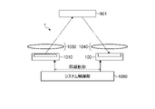
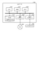
- FIG. 1 is a schematic diagram showing a schematic configuration example of an electronic device equipped with a solid-state image sensor according to the first embodiment
- FIG. 2 is a schematic diagram showing a schematic configuration example of the electronic device according to the first embodiment. It is a block diagram which shows the system configuration example.
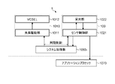
- the electronic device 1 includes a laser light source 1010, an irradiation lens 1030, an image pickup lens 1040, an EVS device 100 as a solid-state image pickup device, and a system control unit 1060.
- the laser light source 1010 is composed of, for example, a vertical resonator type surface emitting laser (VCSEL) 1012 and a light source driving unit 1011 for driving the VCSEL 1012.
- VCSEL vertical resonator type surface emitting laser
- the present invention is not limited to VCSEL1012, and various light sources such as LEDs (Light Emitting Diode) may be used.
- the laser light source 1010 may be any of a point light source, a surface light source, and a line light source.
- the laser light source 1010 may include, for example, a configuration in which a plurality of point light sources (for example, VCSEL) are arranged one-dimensionally or two-dimensionally.
- the laser light source 1010 may emit light having a wavelength band different from that of visible light, such as infrared (IR) light.
- IR infrared
- the irradiation lens 1030 is arranged on the emission surface side of the laser light source 1010, and converts the light emitted from the laser light source 1010 into irradiation light having a predetermined spread angle.
- the image pickup lens 1040 is arranged on the light receiving surface side of the EVS device 100, and an image of incident light is formed on the light receiving surface of the EVS device 100.
- the incident light may also include reflected light emitted from the laser light source 1010 and reflected by the subject 901.
- the EVS device 100 The details of the EVS device 100 will be described later, but as shown in FIG. 3, for example, the light receiving unit 1022 and the light receiving unit 1022 in which pixels for detecting an event (hereinafter referred to as event pixels) are arranged in a two-dimensional grid pattern. It is composed of a sensor control unit 1021 that generates frame data based on the event data detected by the event pixels by driving.
- event pixels pixels for detecting an event
- the system control unit 1060 is configured by, for example, a processor (CPU), and drives the VCSEL 1012 via the light source drive unit 1011. Further, the system control unit 1060 controls the EVS device 100 in synchronization with the control for the laser light source 1010 to acquire event data detected according to the light emission / quenching of the laser light source 1010.
- a processor CPU
- the system control unit 1060 controls the EVS device 100 in synchronization with the control for the laser light source 1010 to acquire event data detected according to the light emission / quenching of the laser light source 1010.
- the irradiation light emitted from the laser light source 1010 is projected onto the subject (also referred to as a measurement object or object) 901 through the irradiation lens 1030.
- This projected light is reflected by the subject 901.
- the light reflected by the subject 901 passes through the image pickup lens 1040 and is incident on the EVS device 100.
- the EVS device 100 receives the reflected light reflected by the subject 901 and generates event data, and generates frame data which is one image based on the generated event data.
- the frame data generated by the EVS device 100 is supplied to the application processor 1070 of the electronic device 1.
- the application processor 1070 as an information processing device executes predetermined processing such as image processing and recognition processing on the frame data input from the EVS device 100.
- FIG. 3 is a block diagram showing a schematic configuration example of the EVS device according to the present embodiment.
- the EVS device 100 includes a pixel array unit 101, an X arbiter 104A and a Y arbiter 104B, an event signal processing circuit 103, a system control circuit 105, and an output interface (I / F) 109. Be prepared.
- the pixel array unit 101 has a configuration in which a plurality of event pixels 20 for detecting an event based on a change in the brightness of incident light are arranged in a two-dimensional grid pattern.
- the row direction also referred to as the row direction
- the column direction also referred to as the column direction
- the direction (vertical direction in the drawing).
- Each event pixel 20 includes a photoelectric conversion element that generates an electric charge according to the brightness of the incident light, and when a change in the brightness of the incident light is detected based on the photocurrent flowing out from the photoelectric conversion element, the event pixel 20 is requested to read from itself.
- the request to be made is output to the X arbiter 104A and the Y arbiter 104B, and an event signal indicating that an event has been detected is output according to the arbitration by the X arbiter 104A and the Y arbiter 104B.
- Each event pixel 20 detects the presence or absence of an event depending on whether or not a change exceeding a predetermined threshold value has occurred in the photocurrent corresponding to the brightness of the incident light. For example, each event pixel 20 detects that the change in luminance exceeds a predetermined threshold value (positive event) or falls below a predetermined threshold value (negative event) as an event.
- the event pixel 20 When the event pixel 20 detects an event, it outputs a request for permission to output an event signal indicating the occurrence of the event to the X arbiter 104A and the Y arbiter 104B, respectively. Then, when the event pixel 20 receives a response indicating permission to output the event signal from each of the X arbiter 104A and the Y arbiter 104B, the event pixel 20 outputs the event signal to the event signal processing circuit 103.
- the X arbiter 104A and the Y arbiter 104B arbitrate the request for the output of the event signal supplied from each of the plurality of event pixels 20, and the response based on the arbitration result (permission / disapproval of the output of the event signal) and the response. , A reset signal for resetting the event detection is transmitted to the event pixel 20 that outputs the request.
- the event signal processing circuit 103 generates and outputs event data by executing predetermined signal processing on the event signal input from the event pixel 20.
- the change in the photocurrent generated by the event pixel 20 can also be regarded as the change in the amount of light (change in brightness) of the light incident on the photoelectric conversion unit of the event pixel 20. Therefore, it can be said that the event is a change in the amount of light (change in brightness) of the event pixel 20 that exceeds a predetermined threshold value.
- the event data representing the occurrence of an event includes at least position information such as coordinates representing the position of the event pixel 20 in which the change in the amount of light as an event has occurred. In addition to the position information, the event data can include the polarity of the change in the amount of light.
- the event data is the relative time when the event occurred. It can be said that the time information representing the above is implicitly included.
- the event signal processing circuit 103 includes time information indicating a relative time when an event such as a time stamp occurs in the event data before the interval between the event data is not maintained as it was when the event occurred. May be good.
- the system control circuit 105 is configured by a timing generator or the like that generates various timing signals, and based on the various timings generated by the timing generator, the X arbiter 104A, the Y arbiter 104B, the event signal processing circuit 103, and the like are used. Drive control is performed.
- the output I / F 109 sequentially outputs the event data output from the event signal processing circuit 103 in line units to the processing device 200.
- FIG. 4 is a circuit diagram showing a schematic configuration example of event pixels according to the first embodiment. Note that FIG. 4 shows a configuration example in which one comparator performs time-division detection of a positive event and a negative event.
- the event may include, for example, a positive event indicating that the change amount of the photocurrent exceeds the upper limit threshold value and a negative event indicating that the change amount is below the lower limit threshold value.
- the event data representing the occurrence of the event may include, for example, one bit indicating the occurrence of the event and one bit indicating the polarity of the event that has occurred.
- the event pixel 20 may be configured to have a function of detecting only positive events or a configuration having a function of detecting only negative events.
- the event pixel 20 includes, for example, a photoelectric conversion unit PD and an address event detection circuit 210.
- the photoelectric conversion unit PD is composed of, for example, a photodiode or the like, and causes an electric charge generated by photoelectric conversion of incident light to flow out as a photocurrent Iphoto .
- the outflowing photocurrent Iphoto flows into the address event detection circuit 210.
- the address event detection circuit 210 includes a light receiving circuit 212, a memory capacity 213, a comparator 214, a reset circuit 215, an inverter 216, and an output circuit 217.
- the light receiving circuit 212 is composed of, for example, a current-voltage conversion circuit, and converts the photocurrent I photo flowing out of the photoelectric conversion unit PD into a voltage V pr .
- the relationship of the voltage V pr with respect to the intensity (luminance) of light is usually a logarithmic relationship. That is, the light receiving circuit 212 converts the photocurrent I photo corresponding to the intensity of the light applied to the light receiving surface of the photoelectric conversion unit PD into a voltage V pr which is a logarithmic function.
- the relationship between the photocurrent I photo and the voltage V pr is not limited to the logarithmic relationship.
- the voltage V pr corresponding to the photocurrent I photo output from the light receiving circuit 212 becomes the inverting ( ⁇ ) input which is the first input of the comparator 214 as the voltage V diff after passing through the memory capacity 213.
- the comparator 214 is usually composed of a differential pair transistor.
- the comparator 214 uses the threshold voltage V b given from the system control circuit 105 as the second input, which is a non-inverting (+) input, and detects positive events and negative events in a time-divided manner. Further, after the positive event / negative event is detected, the event pixel 20 is reset by the reset circuit 215.
- the system control circuit 105 outputs a voltage V on at the stage of detecting a positive event, outputs a voltage V off at the stage of detecting a negative event, and outputs a voltage at the stage of resetting, as a threshold voltage V b .
- Output V reset is set to a value between the voltage V on and the voltage V off , preferably an intermediate value between the voltage V on and the voltage V off .
- the "intermediate value” means that the value is not only a strictly intermediate value but also a substantially intermediate value, and the existence of various variations in design or manufacturing is permissible. Will be done.
- the system control circuit 105 outputs an ON selection signal to the event pixel 20 at the stage of detecting a positive event, outputs an OFF selection signal at the stage of detecting a negative event, and performs a global reset at the stage of resetting. Output a signal (Global Reset).
- the ON selection signal is given as a control signal to the selection switch SW on provided between the inverter 216 and the output circuit 217.
- the OFF selection signal is given as a control signal to the selection switch SW off provided between the comparator 214 and the output circuit 217.
- the comparator 214 compares the voltage V on and the voltage V diff , and when the voltage V diff exceeds the voltage V on , the amount of change in the optical current I photo exceeds the upper limit threshold value.
- the positive event information On indicating that effect is output as a comparison result.
- the positive event information On is inverted by the inverter 216 and then supplied to the output circuit 217 through the selection switch SW on .
- the comparator 214 compares the voltage V off and the voltage V dim , and when the voltage V def falls below the voltage V off , the amount of change in the optical current I photo falls below the lower limit threshold value.
- the negative event information Off indicating that effect is output as a comparison result.
- the negative event information Off is supplied to the output circuit 217 through the selection switch SW off .
- the reset circuit 215 has a reset switch SW RS , a 2-input OR circuit 2151, and a 2-input AND circuit 2152.
- the reset switch SW RS is connected between the inverting (-) input terminal and the output terminal of the comparator 214, and is turned on (closed) to selectively switch between the inverting input terminal and the output terminal. Short circuit.
- the OR circuit 2151 has two inputs, a positive event information On via the selection switch SW on and a negative event information Off via the selection switch SW off .
- the AND circuit 2152 uses the output signal of the OR circuit 2151 as one input and the global reset signal given from the system control circuit 105 as the other input, and either the positive event information On or the negative event information Off is detected and is global.
- the reset switch SW RS is turned on (closed).
- the reset switch SW RS short-circuits between the inverting input terminal and the output terminal of the comparator 214, and performs a global reset for the event pixel 20. conduct.
- the reset operation is performed only for the event pixel 20 in which the event is detected.
- the output circuit 217 has a configuration including a negative event output transistor NM 1 , a positive event output transistor NM 2 , and a current source transistor NM 3 .
- the negative event output transistor NM 1 has a memory (not shown) for holding negative event information Off at its gate portion. This memory consists of the gate parasitic capacitance of the negative event output transistor NM 1 .
- the positive event output transistor NM 2 has a memory (not shown) for holding the positive event information On at its gate portion.
- This memory consists of the gate parasitic capacitance of the positive event output transistor NM 2 .
- the negative event information Off held in the memory of the negative event output transistor NM 1 and the positive event information On held in the memory of the positive event output transistor NM 2 are the current source transistor NM from the system control circuit 105.
- the row selection signal is given to the gate electrode of 3 , each pixel row of the pixel array unit 101 is transferred to the readout circuit 130 through the output line nRxOff and the output line nRxOn.
- the read circuit 130 is, for example, a circuit provided in the event signal processing circuit 103 (see FIG. 3).
- the event pixel 20 has an event detection function of detecting a positive event and detecting a negative event in a time-division manner using one comparator 214 under the control of the system control circuit 105. It has become.
- a method of efficiently transmitting event data so as not to exceed the transmission band a method of compressing event data can be considered.
- Various coding methods can be adopted for compression of event data, but since there are scenes that are not good for each coding method, when event data generated in a scene that is not good is encoded, it is before compression. The amount of data may increase.
- FIG. 5 is a diagram for explaining a case where the amount of data increases due to coding.
- (a) and (b) show the amount of data when one line (one line) of event data output from the EVS device is not encoded, and (c) and (d) are 1
- the amount of data when the event data for a line (1 line) is encoded is shown.
- (a) and (c) indicate a case where the number of events detected in one line is small (1 pixel)
- (b) and (d) indicate a case where the number of events detected in one line is large (1). All pixels) are shown.
- the event data for one line is the case where the number of events detected in one line is small (a) and the case where the number of events is large (b).
- the amount of data is the same for both.
- the amount of data in (c) is compared with the case of (a) without coding.
- the number of events is large (d)
- the amount of data increases as compared with the case without encoding (b).
- the amount of event data is reduced by a plurality of methods, and the event data reduced to the amount of data that does not exceed the transmission band is transmitted via the output I / F 109.
- the output I / F 109 it is possible to suppress the generation of event data that cannot be completely transmitted, and thus it is possible to suppress a decrease in event detection efficiency.
- FIG. 6 is a block diagram showing a schematic configuration example of the event signal processing circuit according to the present embodiment.
- the event signal processing circuit 103 includes a signal processing unit 310, a data amount adjusting unit 320, and a selection unit 330.
- the signal processing unit 310 is based on, for example, an event signal output from the pixel array unit 101 in units of rows, so that the position information (x address, y address) of the pixel in which the event is detected and the polarity of the detected event (x address, y address) ( Event data (x, y, p, t) including p) and a time stamp (t) indicating the time when the event was detected is generated.
- the X arbiter 104A in the EVS device 100 permits the output of the event signal in pixel row units. In that case, the event signal is output to the event signal processing circuit 103 from the event pixels of one or more pixel columns whose output is permitted by the Y arbiter 104B among the event pixels to which the pixel row to which the output is permitted belongs.
- the data amount adjusting unit 320 reduces the amount of data by using each of the plurality of methods for the event data output from the signal processing unit 310, for example, in line units.
- FIG. 7 shows an example of the data amount adjusting unit 320 according to the present embodiment.
- the data amount adjusting unit 320 is, for example, an uncompressed unit 321, a first compression unit 322, a second compression unit 323, a first signal processing unit 324, and a second signal processing unit 325. And. That is, the data amount adjusting unit 320 according to this example has a total of 5 original event data (hereinafter, also referred to as uncompressed data) and 4 types of event data whose data amount has been adjusted by compression and / or signal processing. It is configured to output the type of event data.
- the type of event data output by the data amount adjusting unit 320 is not limited to five types, and may be two or more types.
- the uncompressed unit 321 is composed of, for example, a buffer or the like, and outputs the input event data (hereinafter, also simply referred to as input data) as it is.
- the first compression unit 322 is a compression unit that compresses event data by the first coding method.
- the second compression unit 323 is a compression unit that compresses event data by a second coding method different from the first coding method.
- the second coding method may include a coding method that is the same as the first coding method and whose parameters are different from those of the first coding method.
- the coding method that can be adopted by the first compression unit 322 and the second compression unit 323 may be a lossless coding method that can restore the original event data, or the original event data cannot be restored. It may be a possible irreversible coding scheme.
- An example of the coding method that can be adopted by the first compression unit 322 and the second compression unit 323 will be described later.
- the first signal processing unit 324 is a signal processing unit that adjusts the amount of event data by the first signal processing.
- the second signal processing unit 325 is a signal processing unit that adjusts the amount of event data by a second signal processing different from the first signal processing.
- the second signal processing may include the same signal processing as the first signal processing but whose parameters are different from those of the first signal processing.
- the signal processing that can be adopted by the first signal processing unit 324 and the second signal processing unit 325 may be reversible signal processing that can restore the original event data, or the original event data cannot be restored. It may be possible irreversible signal processing. Examples of signal processing that can be adopted by the first signal processing unit 324 and the second signal processing unit 325 will be described later.
- the selection unit 330 selects event data having a data amount that does not exceed the transmission band of the output I / F 109 from among the two or more types of event data output from the data amount adjustment unit 320, and outputs the selected event data I / Output to F109. For example, the selection unit 330 may output the event data having the smallest data amount among the two or more types of event data output from the data amount adjustment unit 320 to the output I / F 109.
- the selection unit 330 when the data amount of the uncompressed event data exceeds the transmission band of the output I / F 109, the selection unit 330 is among the event data output from the first compression unit 322 and the second compression unit 323. The smaller amount of data may be output to the output I / F 109. Further, when both the event data output from the first compression unit 322 and the second compression unit 323 have a data amount exceeding the transmission band of the output I / F 109, the selection unit 330 has the first signal processing unit 324 and Of the event data output from the second signal processing unit 325, the smaller data amount may be output to the output I / F 109.
- the selection unit 330 may output event data via a path specified from the outside. For example, when uncompressed (or uncompressed unit 321) is selected from the outside, the selection unit 330 may output event data via the uncompressed unit 321 or compressed from the outside (first compression unit 322). And, when any of the second compression unit 323) is selected, the compressed event data may be output via the compression unit of the selected coding method, or signal processing (first signal) may be output from the outside. When either the processing unit 324 or the second signal processing unit 325) is selected, the data amount is reduced by the selected signal processing (for convenience of explanation, this signal processing result is also referred to as event data). May be output.
- the designation from the outside may be, for example, via the system control circuit 105 (see FIG. 3) or may be directly input.
- the selection unit 330 may output two or more types of event data out of the input plurality of types of event data to the output I / F.
- the selection unit 330 may output uncompressed event data and compressed or signal-processed event data to the output I / F. Further, the output of two or more types of event data may be specified from the outside.
- FIG. 8 is a diagram showing event data according to the first example of the present embodiment.
- the event data generated by the signal processing unit 310 is detected as an x address and a y address (x, y) indicating the positions of the event pixels 20 that have detected the event on the pixel array unit 101.
- Event data (x, y, p, t) for each pixel including polarity information (p) indicating the polarity (positive event or negative event) of the event and a time stamp (t) indicating the time when the event was detected. May be.
- event data for each pixel may be input to the data amount adjusting unit 320 from the signal processing unit 310 in order according to the time series of event occurrence.
- FIG. 9 is a diagram showing event data according to the second example of the present embodiment.
- the signal processing unit 310 may generate a count map M1 in which the number of events detected in each pixel in one frame cycle is mapped according to the array of event pixels 20.
- the positive event and the negative event may be counted separately, or the positive event and the negative event may be counted without distinction.
- FIG. 10 is a diagram showing event data according to the third example of the present embodiment.
- the signal processing unit 310 indicates in 2 bits whether a positive event or a negative event is detected in each pixel based on the event signal output from each pixel within one frame cycle.
- Image data hereinafter, also referred to as frame data
- the pixel value of the corresponding pixel may be determined based on the polarity of the last detected event.
- FIG. 11 is a diagram showing event data according to the fourth example of the present embodiment.
- the signal processing unit 310 is frame data composed of the address (x, y) of the event pixel 20 for which an event is detected within one frame cycle and the polarity (p) of the detected event. M3 may be generated.
- the pixel value of each pixel may not include the time stamp (t) because there is a limitation of being within one frame period.
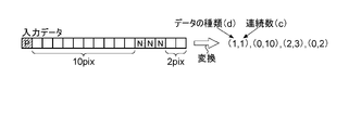
- one line is composed of 16 pixels, a positive event is detected in the first pixel (leftmost pixel) in one line, and a negative event is detected in the 12th to 14th pixels from the beginning.
- An example is an example in which an event is not detected in pixels other than the above.
- the input data to be encoded (compressed) is not limited to the event data for one line, and may be variously modified such as frame data.
- Hcomp coding that converts event data into a data string represented by the address of the pixel in which the event occurred and the polarity of the event is exemplified.
- 12 to 14 are diagrams for explaining the coding of event data for one line using the first coding method (Hcomp coding).
- the y address'y' indicating the corresponding line is stored at the head from the compression unit 3201.
- the set (x i , pi ) of the x address'x i '(i is an integer of 0 or more) of the pixel in which the event was detected and the polarity'pi i'of the detected event is stored.
- Compressed data (hereinafter referred to as output data) is output.
- the output data ((y), (x 0 , p 0 ), (x 1 , p 1 ), (x 2 , p 2 ), (x 3 ) output from the compression unit 3201. , P3)) is the data string of ((y), (0,0), ( 11,1 ), (12,1), (13,1)).
- Run Length coding which converts event data into a data string represented by a data type and the number of consecutive data thereof.
- 15 to 17 are diagrams for explaining the coding of event data for one line using the second coding method (Run Length coding).
- the y address'y' indicating the corresponding line is stored at the beginning from the compression unit 3202. After that, a set ( di , c i ) of a value'di'indicating the type of data (presence or absence of an event and polarity) and a number of consecutive values (consecutive number)' ci ' is stored.
- the compressed data (output data) is output.
- the value (d 2 , c 2 ) (2, 3) indicating that a negative event was detected in three consecutive pixels of, and the event was not detected in the two consecutive pixels from the 15th to the 16th.
- the value indicating that (d 3 , c 3 ) (0, 2).
- the output data ((y), (d 0 , c 0 ), (d 1 , c 1 ), (d 2 , c 2 ), (d 3 ) output from the compression unit 3202. , C 3 )) is a data string of ((y), (1,1), (0,11), (2,3), (0,2)).
- the frequency of appearance of the input data (1,0,0,0,0,0,0,0,0,0,0,0,0,0,2,2,0,0) is high. It can be divided into a bit string of three '2's, a one-time appearance frequency of '0000000000', a one-time appearance frequency of '00', and a one-time appearance frequency of '1'. It should be noted that "0" indicates no event, "1" indicates a positive event, and "2" indicates a negative event. Therefore, as illustrated in FIG.
- the Huffman code '0' is assigned to the bit string '2' and the Huffman code '10 (to the bit string '0000000000').
- the input data is (7, It can be expressed as 2,0,0,0,6).
- the output data ((y), h 0 , h 1 , h 2 , h 3 , h 4 ) output from the compression unit 3203 is ((y), 7, 2, 0). , 0, 0, 6, (frequency table)).
- the compression unit 3204 when input data for one line is input to the compression unit 3204 that employs Light Huffman coding, the compression unit 3204 expresses 1 bit without an event and 2 bits with an event. Output data is output.
- the positive event is represented by 2 bits each of '01'
- the negative event is '10'
- the no event is '00' in the input data.
- the output data is converted into a bit string represented by 2 bits of '11' for a positive event, 2 bits of '10' for a negative event, and 1 bit of '0' for no event.
- the pixel converted to 1 bit is not limited to the pixel without an event, and may be, for example, the type of event (positive event, negative event, or no event) that appears most frequently in one line. ..
- FIGS. 24 to 26 are diagrams for explaining the coding of event data for one line using the fifth coding method (Event Distance coding).
- the output data ((y), (l 0 , p 0 , c 0 ), (l 1 , p 1 , c 1 )) output from the compression unit 3205 is ((y), p 1, c 1). ), (0,0,1), (10,1,3)).
- Entropy coding which converts event data into a data string represented by a distance between events and a pattern of data
- 27 to 29 are diagrams for explaining the coding of event data for one line using the sixth coding method (Entropy coding).
- one line is composed of 16 pixels, positive events are detected in the first, fourth, and sixth pixels in one line, and the fifth, seventh, 12th to 14th pixels from the beginning.
- An example is an example in which a negative event is detected in a pixel and no event is detected in other pixels.
- the compression unit 3206 groups the bit strings of the input data according to a predetermined rule and is based on this group.
- the y address'y'indicating the corresponding line is stored, followed by the value'li'indicating the distance from the immediately preceding same-polarity event, the event polarity'pi', and within the group.
- Output compressed data (output data).
- the compression unit 3206 uses the input data shown in (a) as, for example, an event sequence of a positive event (P) as shown in (b). Negative event (N) Separated from the event column. In the event sequence of the positive event (P) and the event sequence of the negative event (N) shown in (b), the pixel having the event is indicated by "1".
- the compression unit 3206 defines a group for each event column.
- the pixel in which the event is first detected from the beginning is set as the starting point, and the pixels having a predetermined number of pixels from the pixel are set as one group. Therefore, for the event sequence of the positive event (P) shown in FIG. 28 (b), the total number of predetermined pixels (3 in this example) from the first pixel in which the positive event first appears, in order from the left.
- Four pixels that is, the first to fourth pixels
- the 6th to 9th pixels are defined as the group Gp1.
- the event column of the negative event (N) in order from the left, a total of four pixels (that is, 5) from the fifth pixel in which the negative event first appears to a predetermined number of pixels (3 in this example).
- Pixel is defined as group Gn1.
- Data (l 2 , p 2 , s 2 , pt 2 ) (5, 1, 0, 1010) is generated.
- the value'pt i'indicating the arrangement pattern of the same polarity event in the group may be omitted as in the event data of the group Gp1.
- the output data ((y), (l 0 , p 0 , s 0 , pt 0 ), (l 1 , p 1 , s 1 ), (l) output from the compression unit 3206. 2 , p 2 , s 2 , pt 2 ), (l 3 , p 3 , s 3 , pt 3 )) are ((y), (0, 0, 0, 1001), (2, 0, 1)). , (5,1,0,1010), (4,1,0,1110)).
- the signal processing executed by each of the first signal processing unit 324 and the second signal processing unit 325 is also an example of a method for adjusting the amount of event data.
- Optical Flow calculation, feature point extraction, and ROI (Region Of Interest) extraction are exemplified, but the present invention is not limited to these, and various signal processing such as object recognition and noise reduction may be applied.
- DNN Deep Neural Network
- CNN Convolution Neural Network
- RNN Recurrent Neural Network
- other signal processing using machine learning may be applied.
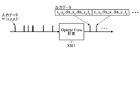
- FIG. 30 is a diagram for explaining the first signal processing (Optical Flow calculation).
- the input data to the signal processing unit 3301 in which the Optical Flow calculation is adopted may be any of the event data exemplified above with reference to FIGS. 8 to 11 or other event data such as frame data. In this description, the case where the event data according to the first example illustrated with reference to FIG. 8 is input data is illustrated.
- the signal processing unit 3301 reconstructs the frame data from the event data input during one frame period, and is reconstructed this time with the frame data of one or more previous frames previously reconstructed.
- the optical flow for each block is calculated from the frame data of the current frame.
- the calculated optical flow may include, for example, the movement amount and the movement speed of each block.
- the block may be one pixel or an area of M ⁇ N pixels (both M and N are integers of 1 or more).
- the signal processing unit 3301 indicates the address ( xi , y i ) indicating the position of the block and the optical in the x direction of the block for each block constituting the frame data.
- Output data ( xi , y i , dis_x i , dis_y i ) including dis_x i indicating the flow and dis_y i indicating the optical flow in the y direction of the block is generated.
- the output data may include a time stamp't j '(j is an integer of 1 or more) as time information indicating the time of the current frame.
- FIG. 31 is a diagram for explaining the second signal processing (feature point extraction).
- the input data to the signal processing unit 3302 in which the feature point extraction is adopted is the event data or the frame data exemplified by using FIGS. 8 to 11 above, as in the first signal processing in which the optical flow calculation is adopted. It may be any of other event data such as. In this description, the case where the event data according to the first example illustrated with reference to FIG. 8 is input data is illustrated.
- the signal processing unit 3302 reconstructs frame data from event data input during one frame period, and executes a process of extracting feature points from the reconstructed frame data. Then, the signal processing unit 3302 generates output data (xi i , y i ) including addresses (xi i , y i ) indicating the positions of the extracted feature points.
- the output data may include a time stamp't j'as time information indicating the time of the current frame.
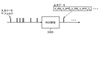
- FIG. 32 is a diagram for explaining a third signal processing (ROI extraction).
- the input data to the signal processing unit 3303 in which ROI extraction is adopted is the same as the first and second signal processing described above, in addition to the event data or frame data exemplified above using FIGS. 8 to 11. It may be any of the event data of. In this description, the case where the event data according to the first example illustrated with reference to FIG. 8 is input data is illustrated.
- the signal processing unit 3303 reconstructs the frame data from the event data input during one frame period, and executes a process of extracting the ROI from the reconstructed frame data. Then, the signal processing unit 3302 includes output data (x_sta i , x_end i ) including an address (x_sta i , y_sta i ) indicating the start point position of the extracted ROI and an address (x_end i , y_end i ) indicating the end point position. , Y_sta i , y_end i ) is generated.
- the output data may include a time stamp't j'as time information indicating the time of the current frame.
- the signal processing unit 3303 cuts out as ROI from the frame data as shown in FIG. 33 in addition to the output data indicating the ROI position calculated as described above or instead of the output data indicating the ROI position.
- the image data G31 may be output.
- Output I / F109 includes, for example, MIPI (Mobile Industry Processor Interface) CSI (Camera Serial Interface) -2 (C-PHY, D-PHY, etc.), I3C (Improved Inter Integrated Circuits), and ALPDP (Acquisition Law Professional Development Program). ) And other interface standards can be adopted. When these interface standards are adopted, the output I / F 109 can output the event data after adjusting the data amount to the outside in frame units. Therefore, in the following, the output of frame data when MIPI CSI-2 is adopted will be described with some examples.
- MIPI Mobile Industry Processor Interface
- CSI Camera Serial Interface
- I3C Improved Inter Integrated Circuits
- ALPDP Acquisition Law Professional Development Program
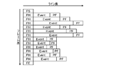
- FIG. 34 is a schematic diagram showing an output form of frame data according to the first output example.
- a frame header FS indicating the beginning of frame data
- a line header PH indicating the beginning of each line data
- a line footer PF indicating the end of each line data
- a line header In a configuration in which the line data event sandwiched between the PH and the line footer PF and the frame footer FE indicating the end of the frame data are output, frame data is inserted between the frame header FS and the frame footer FE. The line data event of all the constituent lines is included.
- y address indicating the position of the line and the line data thereof. May include a flag or the like indicating whether the data is uncompressed data, the data is compressed by any coding method, or the processing result of which signal processing.
- the line data event is the encoded compressed data. Therefore, it is also possible to use the output form exemplified below.
- FIG. 35 is a schematic diagram showing an output form of frame data according to the second output example.
- the data amount of the line data event sandwiched between the line header PH and the line footer PF is the data. It is reduced by the processing by the amount adjusting unit 320. As a result, the amount of data in one frame output from the output I / F 109 is reduced.
- FIG. 36 is a schematic diagram showing an output form of frame data according to the third output example.
- the output of the line data event is omitted for the line in which the event is not detected.
- the amount of data in one frame output from the output I / F 109 is reduced.
- FIG. 37 is a schematic diagram showing an output form of frame data according to the fourth output example.
- the fourth output example by combining the above-mentioned second output example and the third output example, the amount of data of the line data event sandwiched between the line header PH and the line footer PF. Is reduced, and the output of the line data event is omitted for the line in which the event is not detected. As a result, the amount of data in one frame output from the output I / F 109 is further reduced.
- FIG. 38 is a schematic diagram showing an output form of frame data according to the fifth output example.
- the amount of data of the line data event sandwiched between the line header PH and the line footer PF is reduced, so that the data transfer time for one line is shortened. Will be done. Therefore, in the fifth output example, the output interval of the horizontal synchronization signal is made variable according to the data transfer amount of each line. For example, for each line, a horizontal synchronization signal is output at the timing when the output of the line footer PF is completed. As a result, the transfer time of each line can be shortened, so that the transfer time of one frame data can be shortened. Needless to say, when the data transfer for the line in which the event is not detected is omitted, the transfer time is further shortened.
- the amount of event data to be output is adjusted by a plurality of methods (including uncompressed), and the compressed data (including uncompressed data) obtained is obtained.
- the compressed data including uncompressed data
- it is provided with a configuration capable of selectively outputting compressed data in an amount of data that does not exceed the transmission band. As a result, it is possible to reduce the possibility that event data that cannot be transmitted is generated, and it is possible to suppress a decrease in event detection efficiency due to the destruction of event data.
- the electronic device and the solid-state image sensor according to the present embodiment may be the same as the electronic device 1 and the solid-state image sensor (EVS device 100) described with reference to FIGS. 1 to 4 in the first embodiment.
- the event signal processing circuit 103 in the EVS device 100 is replaced with the event signal processing circuit 203 shown in FIG. 39.
- FIG. 39 is a block diagram showing a schematic configuration example of the event signal processing circuit according to the present embodiment.
- the event signal processing circuit 203 includes a signal processing unit 310, a scene determination unit 340, and a data amount adjusting unit 320.
- the signal processing unit 310 and the data amount adjusting unit 320 may be, for example, the same as those according to the first embodiment.
- the scene determination unit 340 determines the current scene based on, for example, event data input from the signal processing unit 310, and based on the determined scene, a coding method (including uncompressed) suitable for the current scene. And / or signal processing (hereinafter, also referred to as a path) is selected from the data amount adjusting unit 320. Then, the scene determination unit 340 is one or more of one or more selected paths (non-compression unit 321, first compression unit 322, second compression unit 323, first signal processing unit 324, and second signal processing unit 325). ), The event data input from the signal processing unit 310 is input. As a result, compressed data (including uncompressed data) generated by coding or signal processing is output from the path in which the event data is input to the output I / F 109.
- an event number analysis algorithm for example, the current scene is determined from the number of event data detected within a predetermined period (for example, one frame period).
- the firing rate analysis algorithm for example, the current scene is determined by analyzing the firing rate of an event using a probability model.
- the cluster analysis algorithm for example, the event data is classified into clusters based on the address of the pixel in which the event is detected, the polarity of the event, and the like, and the result is analyzed to determine the current scene.
- the scene determination using machine learning for example, the current scene is determined by inputting the input event data into the trained model and evaluating the result.
- the method is not limited to these methods, and various scene determination methods may be used.
- the current scene is determined before the event data is encoded / signal processed, and a suitable coding method (uncompressed) estimated from the determined scene is used.
- Event data is input to) and / or signal processing.
- the operation of unused paths one or more of the non-compressed section 321 and the first compressed section 322, the second compressed section 323, the first signal processing section 324, and the second signal processing section 325) can be stopped. Therefore, it is possible to suppress an increase in power consumption of the EVS device 100.
- the selection unit 330 is the amount of data that does not exceed the transmission band from among the two or more compressed data (including uncompressed data) input via each of the two or more paths selected by the scene determination unit 340.
- One or more compressed data may be output to the output I / F 109.
- FIG. 41 is a hardware configuration diagram showing an example of a computer 1000 that realizes the functions of the processing apparatus 200/600.
- the computer 1000 has a CPU 1100, a RAM 1200, a ROM (Read Only Memory) 1300, an HDD (Hard Disk Drive) 1400, a communication interface 1500, and an input / output interface 1600.
- Each part of the computer 1000 is connected by a bus 1050.
- the CPU 1100 operates based on the program stored in the ROM 1300 or the HDD 1400, and controls each part. For example, the CPU 1100 expands the program stored in the ROM 1300 or the HDD 1400 into the RAM 1200, and executes processing corresponding to various programs.
- the ROM 1300 stores a boot program such as a BIOS (Basic Input Output System) executed by the CPU 1100 when the computer 1000 is started, a program depending on the hardware of the computer 1000, and the like.
- BIOS Basic Input Output System
- the HDD 1400 is a computer-readable recording medium that non-temporarily records a program executed by the CPU 1100 and data used by such a program.
- the HDD 1400 is a recording medium for recording a projection control program according to the present disclosure, which is an example of program data 1450.
- the communication interface 1500 is an interface for the computer 1000 to connect to an external network 1550 (for example, the Internet).
- the CPU 1100 receives data from another device or transmits data generated by the CPU 1100 to another device via the communication interface 1500.
- the input / output interface 1600 has a configuration including the above-mentioned I / F unit 18, and is an interface for connecting the input / output device 1650 and the computer 1000.
- the CPU 1100 receives data from an input device such as a keyboard or mouse via the input / output interface 1600. Further, the CPU 1100 transmits data to an output device such as a display, a speaker, or a printer via the input / output interface 1600.
- the input / output interface 1600 may function as a media interface for reading a program or the like recorded on a predetermined recording medium (media).
- the media is, for example, an optical recording medium such as DVD (Digital Versatile Disc) or PD (Phase change rewritable Disk), a magneto-optical recording medium such as MO (Magneto-Optical disk), a tape medium, a magnetic recording medium, or a semiconductor memory.
- an optical recording medium such as DVD (Digital Versatile Disc) or PD (Phase change rewritable Disk)
- a magneto-optical recording medium such as MO (Magneto-Optical disk)
- tape medium such as DVD (Digital Versatile Disc) or PD (Phase change rewritable Disk)
- MO Magneto-optical disk
- the CPU 1100 of the computer 1000 executes the program loaded on the RAM 1200 to execute the event data processing unit 202 and the RGB data processing unit. It realizes at least one function of 402, ToF data processing unit 502, object recognition processing unit 204, and display information generation unit 205. Further, the program and the like related to the present disclosure are stored in the HDD 1400. The CPU 1100 reads the program data 1450 from the HDD 1400 and executes the program, but as another example, these programs may be acquired from another device via the external network 1550.
- the present technology can also have the following configurations.
- a pixel array unit in which a plurality of pixels for detecting a change in the brightness of incident light are arranged in a two-dimensional grid pattern, respectively.
- a signal processing unit that generates first event data including position information of one or more pixels that have detected a change in luminance, and An adjustment unit that adjusts the amount of data of the first event data to generate the second event data, and An output unit that outputs the second event data to the outside, Equipped with
- the adjusting unit includes a plurality of paths for adjusting the amount of the first event data and generating the second event data by different methods.
- the output unit is a solid-state image pickup device that outputs at least one of the second event data output from each of the plurality of paths to the outside.
- the solid-state image pickup device wherein the plurality of paths include one or more first paths that generate the second event data by encoding the first event data.
- the one or more first paths encode the first event data using at least one of Hcomp coding, Run Length coding, Huffman coding, Light Huffman coding, Event Solid coding, and Entropy coding.
- the solid-state imaging device according to (2) above.
- Solid-state image sensor Solid-state image sensor.
- the second path of one or more includes the path for signal processing the first event data using at least one of Optical Flow calculation, feature point extraction, and ROI (Region Of Interest) extraction in (4).
- the adjusting unit inputs the first event data input from the signal processing unit to each of the plurality of paths, and inputs the second event data output from each of the plurality of paths to the output unit.
- the solid-state image sensor according to any one of (1) to (6), wherein the output unit outputs one or more of the second event data output from each of the plurality of paths to the outside.
Landscapes
- Engineering & Computer Science (AREA)
- Multimedia (AREA)
- Signal Processing (AREA)
- Compression Or Coding Systems Of Tv Signals (AREA)
- Image Processing (AREA)
- Studio Devices (AREA)
- Solid State Image Pick-Up Elements (AREA)
- Transforming Light Signals Into Electric Signals (AREA)
Abstract
Description
1.第1の実施形態
1.1 システム構成例
1.2 EVSデバイスの概略構成例
1.3 単位画素の回路構成例
1.4 データ伝送について
1.5 イベント信号処理回路の概略構成例
1.6 イベントデータの例
1.7 符号化方式の例
1.7.1 第1の符号化方式
1.7.2 第2の符号化方式
1.7.3 第3の符号化方式
1.7.4 第4の符号化方式
1.7.5 第5の符号化方式
1.8 信号処理の例
1.8.1 第1の信号処理
1.8.2 第2の信号処理
1.8.3 第3の信号処理
1.9 フレームデータの出力例
1.9.1 第1出力例
1.9.2 第2出力例
1.9.3 第3出力例
1.9.4 第4出力例
1.9.5 第5出力例
1.10 まとめ
2.第2の実施形態
2.1 イベント信号処理回路の概略構成例
2.2 まとめ
2.3 変形例
3.ハードウエア構成
まず、第1の実施形態について、図面を参照して詳細に説明する。
図1は、第1の実施形態に係る固体撮像装置を搭載する電子機器の概略構成例を示す模式図であり、図2は、第1の実施形態に係る電子機器のシステム構成例を示すブロック図である。
つづいて、EVSデバイス100の概略構成例について説明する。図3は、本実施形態に係るEVSデバイスの概略構成例を示すブロック図である。図3に示すように、EVSデバイス100は、画素アレイ部101と、Xアービタ104A及びYアービタ104Bと、イベント信号処理回路103と、システム制御回路105と、出力インタフェース(I/F)109とを備える。
システム制御回路105は、各種のタイミング信号を生成するタイミングジェネレータなどによって構成され、当該タイミングジェネレータで生成された各種のタイミングを基に、Xアービタ104A、Yアービタ104B、及び、イベント信号処理回路103などの駆動制御を行う。
次に、イベント画素20の回路構成例について説明する。図4は、第1の実施形態に係るイベント画素の概略構成例を示す回路図である。なお、図4には、正イベントの検出及び負イベントの検出を1つのコンパレータが時分割で行う場合の構成例が示されている。
以上のような構成を備えるEVSデバイス100からは、各画素で生成されたイベントデータが出力I/F109を介して外部へ出力されるが、伝送帯域を超えるデータ量のイベントデータが発生した場合、伝送しきれないイベントデータを破棄しなければならず、イベントの検出効率が低下してしまうという課題が存在した。
イベントデータのデータ量の削減は、例えば、EVSデバイス100におけるイベント信号処理回路103において実行される。図6は、本実施形態に係るイベント信号処理回路の概略構成例を示すブロック図である。図6に示すように、イベント信号処理回路103は、信号処理部310と、データ量調整部320と、選択部330とを備える。
信号処理部310は、画素アレイ部101から例えば行単位で出力されたイベント信号に基づくことで、イベントが検出された画素の位置情報(xアドレス、yアドレス)と、検出されたイベントの極性(p)と、イベントが検出された時間を示すタイムスタンプ(t)とを含むイベントデータ(x,y,p,t)を生成する。なお、EVSデバイス100におけるXアービタ104Aは、画素行単位でイベント信号の出力を許可するものとする。その場合、出力が許可された画素行の属するイベント画素のうち、Yアービタ104Bによって出力が許可された1以上の画素列のイベント画素から、イベント信号がイベント信号処理回路103へ出力される。
データ量調整部320は、信号処理部310から例えば行単位で出力されたイベントデータに対し、複数の方式それぞれを用いてデータ量の削減を実行する。ここで、図7に、本実施形態に係るデータ量調整部320の一例を示す。
選択部330は、データ量調整部320から出力された2種類以上のイベントデータのうち、出力I/F109の伝送帯域を超えないデータ量のイベントデータを選択し、選択したイベントデータを出力I/F109へ出力する。例えば、選択部330は、データ量調整部320から出力された2種類以上のイベントデータのうち、データ量の最も小さいイベントデータを出力I/F109へ出力してもよい。
次に、信号処理部310からデータ量調整部320に入力されるイベントデータについて、いくつか例を挙げて説明する。
図8は、本実施形態の第1例に係るイベントデータを示す図である。図8に示すように、信号処理部310で生成されるイベントデータは、イベントを検出したイベント画素20の画素アレイ部101上の位置を示すxアドレス及びyアドレス(x,y)と、検出されたイベントの極性(正イベント又は負イベント)を示す極性情報(p)と、イベントが検出された時刻を示すタイムスタンプ(t)とを含む画素ごとのイベントデータ(x,y,p,t)であってもよい。また、信号処理部310からデータ量調整部320へは、イベント発生の時系列に従って順番に、画素ごとのイベントデータが入力されてもよい。
図9は、本実施形態の第2例に係るイベントデータを示す図である。図9に示すように、信号処理部310は、1フレーム周期内に各画素で検出されたイベントの数をイベント画素20の配列に従ってマッピングしたカウントマップM1を生成してもよい。なお、カウントマップM1の生成では、正イベントと負イベントとが分けてカウントされてもよいし、正イベントと負イベントとが区別されずにカウントされてもよい。
図10は、本実施形態の第3例に係るイベントデータを示す図である。図10に示すように、信号処理部310は、1フレーム周期内に各画素から出力されたイベント信号に基づいて、各画素で正イベントと負イベントとのいずれが検出されたかを2ビットで示す画像データ(以下、フレームデータともいう)M2を生成してもよい。その際、同一のフレーム期間内に正イベントと負イベントとの両方が検出された画素については、最後に検出されたイベントの極性に基づいて該当する画素の画素値が決定されてもよい。
図11は、本実施形態の第4例に係るイベントデータを示す図である。図11に示すように、信号処理部310は、1フレーム周期内にイベントを検出したイベント画素20のアドレス(x,y)と、検出されたイベントの極性(p)とから構成されたフレームデータM3を生成してもよい。その場合、1フレーム周期内という制限が存在するため、各画素の画素値には、タイムスタンプ(t)が含まれていなくてもよい。
つづいて、上述した第1圧縮部322及び第2圧縮部323に適用され得る符号化方式について、いくつか例を挙げて説明する。なお、以下では、Hcomp coding、Run Length coding、Huffman coding、Light Huffman coding、Event Distance coding、Entropy codingを例示するが、これらに限定されず、例えば、ISSCC(IEEE International Solid-State Circuits Conference)2017 4.1に係る符号化方式や、ISSCC2020 5.10に係る符号化方式など、種々の符号化方式が採用されてよい。また、以下の説明では、1ラインが16画素で構成され、1ラインにおける先頭画素(左端の画素)で正イベントが検出され、先頭から12番目~14番目の画素で負イベントが検出され、それ以外の画素ではイベントが検出されなかった場合を例示する。ただし、符号化(圧縮)対象の入力データは、1ライン分のイベントデータに限定されず、フレームデータなど、種々変形されてよい。
第1の符号化方式としては、イベントデータをイベントが発生した画素のアドレスとイベントの極性とで表現されたデータ列に変換するHcomp codingを例示する。図12~図14は、第1の符号化方式(Hcomp coding)を用いた1ライン分のイベントデータの符号化を説明するための図である。
第2の符号化方式としては、イベントデータをデータの種類とその連続数とで表現されたデータ列に変換するRun Length codingを例示する。図15~図17は、第2の符号化方式(Run Length coding)を用いた1ライン分のイベントデータの符号化を説明するための図である。
第3の符号化方式としては、イベントデータをイベントの出現頻度に応じた表現のデータ列に変換するHuffman codingを例示する。図18~図20は、第3の符号化方式(Huffman coding)を用いた1ライン分のイベントデータの符号化を説明するための図である。
第4の符号化方式としては、イベントデータをイベント無しが1ビット、イベントありが2ビットで表現されたデータ列に変換するLight Huffman codingを例示する。図21~図23は、第4の符号化方式(Light Huffman coding)を用いた1ライン分のイベントデータの符号化を説明するための図である。
第5の符号化方式としては、イベントデータをイベント間の距離で表現されたデータ列に変換するEvent Distance codingを例示する。図24~図26は、第5の符号化方式(Event Distance coding)を用いた1ライン分のイベントデータの符号化を説明するための図である。
第6の符号化方式としては、イベントデータをイベント間の距離とデータのパターンとで表現されたデータ列に変換するEntropy codingを例示する。図27~図29は、第6の符号化方式(Entropy coding)を用いた1ライン分のイベントデータの符号化を説明するための図である。なお、本説明では、理解のため、1ラインが16画素で構成され、1ラインにおける先頭から1、4及び6番目の画素で正イベントが検出され、先頭から5、7、12~14番目の画素で負イベントが検出され、それ以外の画素ではイベントが検出されなかった場合を例示する。
つづいて、上述した第1信号処理部324及び第2信号処理部325に適用され得る信号処理について、いくつか例を挙げて説明する。なお、第1信号処理部324及び第2信号処理部325それぞれが実行する信号処理も、イベントデータのデータ量を調整する方式の例である。また、以下では、Optical Flow計算、特徴点抽出、ROI(Region Of Interest)抽出を例示するが、これらに限定されず、物体認識やノイズリダクションなどの種々の信号処理が適用されてもよく、また、DNN(Deep Neural Network)やCNN(Convolution Neural Network)やRNN(Recurrent Neural Network)などの機械学習を利用した信号処理が適用されてもよい。
第1の信号処理としては、入力されたイベントデータから再構成されるフレームデータに対してOptical Flow計算を実行する場合を例示する。図30は、第1の信号処理(Optical Flow計算)を説明するための図である。
第2の信号処理としては、入力されたイベントデータから再構成されるフレームデータに対して特徴点抽出を実行する場合を例示する。図31は、第2の信号処理(特徴点抽出)を説明するための図である。
第3の信号処理としては、入力されたイベントデータから再構成されるフレームデータに対してROI抽出を実行する場合を例示する。図32は、第3の信号処理(ROI抽出)を説明するための図である。
つづいて、出力I/F109によるフレームデータの出力形態について、いくつか例を挙げて説明する。
図34は、第1出力例に係るフレームデータの出力形態を示す模式図である。図34に示すように、第1出力例では、フレームデータの先頭を示すフレームヘッダFSと、各ラインデータの先頭を示すラインヘッダPHと、各ラインデータの末尾を示すラインフッタPFと、ラインヘッダPHとラインフッタPFとの間に挟まれたラインデータEventと、フレームデータの末尾を示すフレームフッタFEとが出力される構成において、フレームヘッダFSとフレームフッタFEとの間には、フレームデータを構成する全てのラインのラインデータEventが含まれる。
図35は、第2出力例に係るフレームデータの出力形態を示す模式図である。図35に示すように、第2出力例では、第1出力例に係る出力形態と同様の形態において、ラインヘッダPHとラインフッタPFとの間に挟まれたラインデータEventのデータ量が、データ量調整部320による処理により削減されている。それにより、出力I/F109から出力される1フレームのデータ量が削減されている。
図36は、第3出力例に係るフレームデータの出力形態を示す模式図である。図36に示すように、第3出力例では、第1出力例に係る出力形態と同様の形態において、イベントが検出されていないラインについては、ラインデータEventの出力が省略されている。それにより、出力I/F109から出力される1フレームのデータ量が削減されている。
図37は、第4出力例に係るフレームデータの出力形態を示す模式図である。図37に示すように、第4出力例では、上述した第2出力例と第3出力例とを組み合わせることで、ラインヘッダPHとラインフッタPFとの間に挟まれたラインデータEventのデータ量が削減されるとともに、イベントが検出されていないラインについてはラインデータEventの出力が省略されている。それにより、出力I/F109から出力される1フレームのデータ量がより削減されている。
図38は、第5出力例に係るフレームデータの出力形態を示す模式図である。上述した第2出力例及び第4出力例では、ラインヘッダPHとラインフッタPFとの間に挟まれたラインデータEventのデータ量が削減されているため、1ライン分のデータの転送時間が短縮される。そこで第5出力例では、各ラインのデータ転送量に応じて水平同期信号の出力間隔を可変にする。例えば、各ラインについて、ラインフッタPFの出力が完了したタイミングで水平同期信号を出力する。それにより、各ラインの転送時間を短縮することが可能となるため、1フレームデータの転送時間を短縮することが可能となる。なお、イベントが検出されていないラインについてのデータ転送を省略する場合には、それにより転送時間がより短縮されることは言うまでもない。
以上のように、本実施形態は、出力対象であるイベントデータのデータ量を複数の手法(非圧縮を含む)により調整し、得られた圧縮データ(非圧縮データを含む)のうち、伝送帯域を超えないデータ量の圧縮データを選択的に出力し得る構成を備える。それにより、伝送しきれないイベントデータが発生する可能性を低減することが可能となるため、イベントデータの破棄によるイベント検出効率の低下を抑制することが可能となる。
次に、第2の実施形態について、図面を参照して詳細に説明する。なお、以下の説明において、上述した実施形態と同様の構成については、それらを引用することで重複する説明を省略する。
図39は、本実施形態に係るイベント信号処理回路の概略構成例を示すブロック図である。図39に示すように、イベント信号処理回路203は、信号処理部310と、シーン判定部340と、データ量調整部320とを備える。信号処理部310及びデータ量調整部320は、例えば、第1の実施形態に係るそれらと同様であってよい。
シーン判定部340は、例えば、信号処理部310から入力されたイベントデータに基づいて現在のシーンを判定し、判定したシーンに基づいて、現在のシーンに適した符号化方式(非圧縮を含む)及び/又は信号処理(以下、パスともいう)をデータ量調整部320の中から選択する。そして、シーン判定部340は、選択した1以上のパス(非圧縮部321、第1圧縮部322、第2圧縮部323、第1信号処理部324及び第2信号処理部325のいずれか1以上)へ、信号処理部310から入力されたイベントデータを入力する。それにより、イベントデータが入力されたパスから出力I/F109へ、符号化又は信号処理により生成された圧縮データ(非圧縮データを含む)が出力される。
以上のように、本実施形態では、イベントデータを符号化/信号処理する前に、現在のシーンを判定し、判定されたシーンから推定される好適な符号化方式(非圧縮を含む)及び/又は信号処理へイベントデータが入力される。それにより、使用しないパス(非圧縮部321、第1圧縮部322、第2圧縮部323、第1信号処理部324及び第2信号処理部325のいずれか1以上)の動作を停止することが可能となるため、EVSデバイス100の消費電力増加を抑制することが可能となる。
なお、図40に示すように、上述した第1の実施形態に係る構成と第2の実施形態に係る構成とを組み合わせることも可能である。その場合、選択部330は、シーン判定部340により選択された2以上のパスそれぞれを経由して入力された2以上の圧縮データ(非圧縮データを含む)の中から伝送帯域を超えないデータ量の1以上の圧縮データ(非圧縮データを含む)を出力I/F109へ出力してもよい。
上述してきた実施形態及びその変形例並びに応用例に係る処理装置200/600は、例えば図41に示すような構成のコンピュータ1000によって実現され得る。図41は、処理装置200/600の機能を実現するコンピュータ1000の一例を示すハードウエア構成図である。コンピュータ1000は、CPU1100、RAM1200、ROM(Read Only Memory)1300、HDD(Hard Disk Drive)1400、通信インタフェース1500、及び入出力インタフェース1600を有する。コンピュータ1000の各部は、バス1050によって接続される。
(1)
それぞれ入射光の輝度変化を検出する複数の画素が2次元格子状に配列する画素アレイ部と、
輝度変化を検出した1以上の画素の位置情報を含む第1イベントデータを生成する信号処理部と、
前記第1イベントデータのデータ量を調整して第2イベントデータを生成する調整部と、
前記第2イベントデータを外部へ出力する出力部と、
を備え、
前記調整部は、それぞれ異なる方式で前記第1イベントデータの前記データ量を調整して第2イベントデータを生成する複数のパスを備え、
前記出力部は、前記複数のパスそれぞれから出力された前記第2イベントデータのうちの少なくとも1つを外部へ出力する
固体撮像装置。
(2)
前記複数のパスは、それぞれ前記第1イベントデータを符号化することで前記第2イベントデータを生成する1以上の第1パスを含む
前記(1)に記載の固体撮像装置。
(3)
前記1以上の第1パスは、Hcomp coding、Run Length coding、Huffman coding、Light Huffman coding、Event Distance coding、及び、Entropy codingのうちの少なくとも1つを用いて前記第1イベントデータを符号化するパスを含む
前記(2)に記載の固体撮像装置。
(4)
前記複数のパスは、それぞれ前記第1イベントデータを信号処理することで前記第2イベントデータを生成する1以上の第2パスを含む
前記(1)~(3)の何れか1つに記載の固体撮像装置。
(5)
前記1以上の第2パスは、Optical Flow計算、特徴点抽出、ROI(Region Of Interest)抽出のうちの少なくとも1つを用いて前記第1イベントデータを信号処理するパスを含む
前記(4)に記載の固体撮像装置。
(6)
前記複数のパスは、前記第1イベントデータをそのまま出力する第3パスを含む
前記(1)~(5)の何れか1つに記載の固体撮像装置。
(7)
前記調整部は、前記信号処理部から入力された前記第1イベントデータを前記複数のパスそれぞれに入力し、前記複数のパスそれぞれから出力された前記第2イベントデータを前記出力部に入力し、
前記出力部は、前記複数のパスそれぞれから出力された前記第2イベントデータのうちの1以上を外部へ出力する
前記(1)~(6)の何れか1つに記載の固体撮像装置。
(8)
前記出力部は、前記複数のパスそれぞれから出力された前記第2イベントデータのうち、伝送帯域を超えないデータ量の第2イベントデータを外部へ出力する
前記(7)に記載の固体撮像装置。
(9)
前記出力部は、前記複数のパスそれぞれから出力された前記第2イベントデータのうち、データ量の最も小さい第2イベントデータを外部へ出力する
前記(7)に記載の固体撮像装置。
(10)
前記第1イベントデータに基づいてシーンを判定する判定部をさらに備え、
前記判定部は、前記第1イベントデータに基づいて判定された前記シーンに基づいて、前記複数のパスのうちの少なくとも1つのパスに前記第1イベントデータを入力する
前記(1)~(6)の何れか1つに記載の固体撮像装置。
(11)
前記出力部は、前記第2イベントデータをフレーム単位で外部へ出力する
前記(1)~(10)の何れか1つに記載の固体撮像装置。
(12)
前記出力部は、各ラインのデータ長が前記調整部により調整されたフレームデータを外部へ出力する
前記(11)に記載の固体撮像装置。
(13)
前記出力部は、入射光の輝度変化が検出された画素が存在しないラインのラインデータを含まないフレームデータを外部へ出力する
前記(11)又は(12)に記載の固体撮像装置。
(14)
前記出力部は、各ラインのラインデータの出力が完了次第、水平同期信号を出力する
前記(11)~(13)の何れか1つに記載の固体撮像装置。
(15)
前記(1)~(14)の何れか1つに記載の固体撮像装置と、
前記固体撮像装置から出力された第2イベントデータを処理する情報処理装置と、
を備える電子機器。
20 イベント画素
100 EVSデバイス(固体撮像装置)
101 画素アレイ部
103、203 イベント信号処理回路
104A Xアービタ
104B Yアービタ
105 システム制御回路
109 出力I/F
310 信号処理部
320 データ量調整部
321 非圧縮部
322 第1圧縮部
323 第2圧縮部
324 第1信号処理部
325 第2信号処理部
330 選択部
340 シーン判定部
3201~3205 圧縮部
3301~3303 信号処理部
1010 レーザ光源
1011 光源駆動部
1012 VCSEL
1021 センサ制御部
1022 受光部
1030 照射レンズ
1040 撮像レンズ
1060 システム制御部
1070 アプリケーションプロセッサ
Claims (15)
- それぞれ入射光の輝度変化を検出する複数の画素が2次元格子状に配列する画素アレイ部と、
輝度変化を検出した1以上の画素の位置情報を含む第1イベントデータを生成する信号処理部と、
前記第1イベントデータのデータ量を調整して第2イベントデータを生成する調整部と、
前記第2イベントデータを外部へ出力する出力部と、
を備え、
前記調整部は、それぞれ異なる方式で前記第1イベントデータの前記データ量を調整して第2イベントデータを生成する複数のパスを備え、
前記出力部は、前記複数のパスそれぞれから出力された前記第2イベントデータのうちの少なくとも1つを外部へ出力する
固体撮像装置。 - 前記複数のパスは、それぞれ前記第1イベントデータを符号化することで前記第2イベントデータを生成する1以上の第1パスを含む
請求項1に記載の固体撮像装置。 - 前記1以上の第1パスは、Hcomp coding、Run Length coding、Huffman coding、Light Huffman coding、Event Distance coding、及び、Entropy codingのうちの少なくとも1つを用いて前記第1イベントデータを符号化するパスを含む
請求項2に記載の固体撮像装置。 - 前記複数のパスは、それぞれ前記第1イベントデータを信号処理することで前記第2イベントデータを生成する1以上の第2パスを含む
請求項1に記載の固体撮像装置。 - 前記1以上の第2パスは、Optical Flow計算、特徴点抽出、ROI(Region Of Interest)抽出のうちの少なくとも1つを用いて前記第1イベントデータを信号処理するパスを含む
請求項4に記載の固体撮像装置。 - 前記複数のパスは、前記第1イベントデータをそのまま出力する第3パスを含む
請求項1に記載の固体撮像装置。 - 前記調整部は、前記信号処理部から入力された前記第1イベントデータを前記複数のパスそれぞれに入力し、前記複数のパスそれぞれから出力された前記第2イベントデータを前記出力部に入力し、
前記出力部は、前記複数のパスそれぞれから出力された前記第2イベントデータのうちの1以上を外部へ出力する
請求項1に記載の固体撮像装置。 - 前記出力部は、前記複数のパスそれぞれから出力された前記第2イベントデータのうち、伝送帯域を超えないデータ量の第2イベントデータを外部へ出力する
請求項7に記載の固体撮像装置。 - 前記出力部は、前記複数のパスそれぞれから出力された前記第2イベントデータのうち、データ量の最も小さい第2イベントデータを外部へ出力する
請求項7に記載の固体撮像装置。 - 前記第1イベントデータに基づいてシーンを判定する判定部をさらに備え、
前記判定部は、前記第1イベントデータに基づいて判定された前記シーンに基づいて、前記複数のパスのうちの少なくとも1つのパスに前記第1イベントデータを入力する
請求項1に記載の固体撮像装置。 - 前記出力部は、前記第2イベントデータをフレーム単位で外部へ出力する
請求項1に記載の固体撮像装置。 - 前記出力部は、各ラインのデータ長が前記調整部により調整されたフレームデータを外部へ出力する
請求項11に記載の固体撮像装置。 - 前記出力部は、入射光の輝度変化が検出された画素が存在しないラインのラインデータを含まないフレームデータを外部へ出力する
請求項11に記載の固体撮像装置。 - 前記出力部は、各ラインのラインデータの出力が完了次第、水平同期信号を出力する
請求項11に記載の固体撮像装置。 - 請求項1に記載の固体撮像装置と、
前記固体撮像装置から出力された第2イベントデータを処理する情報処理装置と、
を備える電子機器。
Priority Applications (5)
| Application Number | Priority Date | Filing Date | Title |
|---|---|---|---|
| KR1020237016965A KR20230098222A (ko) | 2020-10-30 | 2021-10-18 | 고체 촬상 장치 및 전자 기기 |
| US18/033,493 US12267608B2 (en) | 2020-10-30 | 2021-10-18 | Solid-state imaging device and electronic device |
| EP21885945.2A EP4240005A4 (en) | 2020-10-30 | 2021-10-18 | SEMICONDUCTOR IMAGING DEVICE AND ELECTRONIC INSTRUMENT |
| JP2022559016A JP7830342B2 (ja) | 2020-10-30 | 2021-10-18 | 固体撮像装置及び電子機器 |
| CN202180072021.2A CN116349242A (zh) | 2020-10-30 | 2021-10-18 | 固态成像设备和电子设备 |
Applications Claiming Priority (2)
| Application Number | Priority Date | Filing Date | Title |
|---|---|---|---|
| JP2020-182095 | 2020-10-30 | ||
| JP2020182095 | 2020-10-30 |
Publications (1)
| Publication Number | Publication Date |
|---|---|
| WO2022091826A1 true WO2022091826A1 (ja) | 2022-05-05 |
Family
ID=81382543
Family Applications (1)
| Application Number | Title | Priority Date | Filing Date |
|---|---|---|---|
| PCT/JP2021/038359 Ceased WO2022091826A1 (ja) | 2020-10-30 | 2021-10-18 | 固体撮像装置及び電子機器 |
Country Status (7)
| Country | Link |
|---|---|
| US (1) | US12267608B2 (ja) |
| EP (1) | EP4240005A4 (ja) |
| JP (1) | JP7830342B2 (ja) |
| KR (1) | KR20230098222A (ja) |
| CN (1) | CN116349242A (ja) |
| TW (1) | TW202236843A (ja) |
| WO (1) | WO2022091826A1 (ja) |
Cited By (4)
| Publication number | Priority date | Publication date | Assignee | Title |
|---|---|---|---|---|
| WO2024135083A1 (en) * | 2022-12-23 | 2024-06-27 | Sony Semiconductor Solutions Corporation | Light detecting device and processing device |
| WO2024203526A1 (ja) * | 2023-03-29 | 2024-10-03 | ソニーセミコンダクタソリューションズ株式会社 | 光検出装置及び電子機器 |
| WO2026004613A1 (ja) * | 2024-06-25 | 2026-01-02 | ソニーセミコンダクタソリューションズ株式会社 | イベントデータ出力センサおよび電子機器 |
| WO2026028805A1 (ja) * | 2024-08-02 | 2026-02-05 | ソニーセミコンダクタソリューションズ株式会社 | データ処理装置およびデータ処理方法、並びに、イベントデータ出力センサ |
Families Citing this family (2)
| Publication number | Priority date | Publication date | Assignee | Title |
|---|---|---|---|---|
| US12184973B2 (en) * | 2023-03-02 | 2024-12-31 | Omnivision Technologies, Inc. | Methods for transmitting asynchronous event data via synchronous communications interfaces, and associated imaging systems |
| US12413869B2 (en) * | 2023-12-28 | 2025-09-09 | Omnivision Technologies, Inc. | Low-power always-on event-based vision sensor |
Citations (3)
| Publication number | Priority date | Publication date | Assignee | Title |
|---|---|---|---|---|
| JP2003116006A (ja) * | 2001-10-05 | 2003-04-18 | Canon Inc | 画像符号化方法及び装置 |
| JP2004248320A (ja) * | 2004-04-21 | 2004-09-02 | Canon Inc | 画像記録再生装置 |
| JP2020127186A (ja) * | 2019-01-31 | 2020-08-20 | ソニーセミコンダクタソリューションズ株式会社 | 固体撮像装置及び撮像装置 |
Family Cites Families (15)
| Publication number | Priority date | Publication date | Assignee | Title |
|---|---|---|---|---|
| US1A (en) | 1836-07-13 | John Ruggles | Locomotive steam-engine for rail and other roads | |
| JP5039425B2 (ja) * | 2007-04-26 | 2012-10-03 | キヤノン株式会社 | 画像符号化装置及びその制御方法 |
| KR101792866B1 (ko) * | 2011-04-06 | 2017-11-20 | 삼성전자주식회사 | 이벤트 센서와 칼라 센서를 이용한 동작 인식 장치 및 그 방법 |
| US10444304B2 (en) | 2014-03-26 | 2019-10-15 | General Electric Company | Particle event recordation |
| US9986179B2 (en) | 2014-09-30 | 2018-05-29 | Qualcomm Incorporated | Sensor architecture using frame-based and event-based hybrid scheme |
| JP2017034531A (ja) * | 2015-08-04 | 2017-02-09 | 富士通株式会社 | 動画像符号化装置及び動画像符号化方法 |
| CN108574793B (zh) * | 2017-03-08 | 2022-05-10 | 三星电子株式会社 | 被配置为重新生成时间戳的图像处理设备及包括其在内的电子设备 |
| US10855927B2 (en) * | 2017-03-08 | 2020-12-01 | Samsung Electronics Co., Ltd. | Event detecting device including an event signal generator and an output signal generator |
| US10582196B2 (en) * | 2017-06-30 | 2020-03-03 | Intel Corporation | Generating heat maps using dynamic vision sensor events |
| EP3506622A1 (en) * | 2017-12-26 | 2019-07-03 | Prophesee | Method for outputting a signal from an event based sensor, and event-based sensor using such method |
| US12566944B2 (en) * | 2018-03-09 | 2026-03-03 | Lattice Semiconductor Corporation | Low latency interrupt alerts for artificial neural network systems and methods in data stream processing |
| KR20190133465A (ko) | 2018-05-23 | 2019-12-03 | 삼성전자주식회사 | 다이나믹 비전 센서의 데이터 처리 방법, 이를 수행하는 다이나믹 비전 센서 및 이를 포함하는 전자 장치 |
| WO2020027233A1 (ja) * | 2018-07-31 | 2020-02-06 | ソニーセミコンダクタソリューションズ株式会社 | 撮像装置及び車両制御システム |
| JP2022028982A (ja) | 2018-12-05 | 2022-02-17 | ソニーセミコンダクタソリューションズ株式会社 | 固体撮像装置、信号処理チップ、および、電子機器 |
| US10893201B2 (en) * | 2019-05-16 | 2021-01-12 | Pelco, Inc. | Video stabilization method with non-linear frame motion correction in three axes |
-
2021
- 2021-09-23 TW TW110135233A patent/TW202236843A/zh unknown
- 2021-10-18 US US18/033,493 patent/US12267608B2/en active Active
- 2021-10-18 EP EP21885945.2A patent/EP4240005A4/en active Pending
- 2021-10-18 WO PCT/JP2021/038359 patent/WO2022091826A1/ja not_active Ceased
- 2021-10-18 CN CN202180072021.2A patent/CN116349242A/zh active Pending
- 2021-10-18 KR KR1020237016965A patent/KR20230098222A/ko active Pending
- 2021-10-18 JP JP2022559016A patent/JP7830342B2/ja active Active
Patent Citations (3)
| Publication number | Priority date | Publication date | Assignee | Title |
|---|---|---|---|---|
| JP2003116006A (ja) * | 2001-10-05 | 2003-04-18 | Canon Inc | 画像符号化方法及び装置 |
| JP2004248320A (ja) * | 2004-04-21 | 2004-09-02 | Canon Inc | 画像記録再生装置 |
| JP2020127186A (ja) * | 2019-01-31 | 2020-08-20 | ソニーセミコンダクタソリューションズ株式会社 | 固体撮像装置及び撮像装置 |
Non-Patent Citations (1)
| Title |
|---|
| See also references of EP4240005A4 |
Cited By (4)
| Publication number | Priority date | Publication date | Assignee | Title |
|---|---|---|---|---|
| WO2024135083A1 (en) * | 2022-12-23 | 2024-06-27 | Sony Semiconductor Solutions Corporation | Light detecting device and processing device |
| WO2024203526A1 (ja) * | 2023-03-29 | 2024-10-03 | ソニーセミコンダクタソリューションズ株式会社 | 光検出装置及び電子機器 |
| WO2026004613A1 (ja) * | 2024-06-25 | 2026-01-02 | ソニーセミコンダクタソリューションズ株式会社 | イベントデータ出力センサおよび電子機器 |
| WO2026028805A1 (ja) * | 2024-08-02 | 2026-02-05 | ソニーセミコンダクタソリューションズ株式会社 | データ処理装置およびデータ処理方法、並びに、イベントデータ出力センサ |
Also Published As
| Publication number | Publication date |
|---|---|
| US12267608B2 (en) | 2025-04-01 |
| EP4240005A1 (en) | 2023-09-06 |
| TW202236843A (zh) | 2022-09-16 |
| JPWO2022091826A1 (ja) | 2022-05-05 |
| KR20230098222A (ko) | 2023-07-03 |
| US20230403482A1 (en) | 2023-12-14 |
| EP4240005A4 (en) | 2023-10-11 |
| CN116349242A (zh) | 2023-06-27 |
| JP7830342B2 (ja) | 2026-03-16 |
Similar Documents
| Publication | Publication Date | Title |
|---|---|---|
| WO2022091826A1 (ja) | 固体撮像装置及び電子機器 | |
| JP7717132B2 (ja) | 動的ビジョンセンサアーキテクチャ | |
| Dong et al. | Spike camera and its coding methods | |
| US11290667B2 (en) | Apparatus for encoding image, apparatus for decoding image and image sensor | |
| US20190364230A1 (en) | Method of processing data for dynamic vision sensor, dynamic vision sensor performing the same and electronic device including the same | |
| CN111885368A (zh) | 用于错误检测和校正的系统和方法 | |
| JP2022108329A (ja) | 情報処理装置、情報処理システム、情報処理方法及びプログラム | |
| WO2022148423A1 (zh) | 运动物体检测方法和装置 | |
| Zhao et al. | Spikingsim: A bio-inspired spiking simulator | |
| Sundar et al. | Generalized event cameras | |
| US20040001074A1 (en) | Image display apparatus and method, transmitting apparatus and method, image display system, recording medium, and program | |
| TW202450331A (zh) | 具有事件資料壓縮之事件視覺感測器,包括具有像素內事件資料壓縮之事件視覺感測器,及相關系統、裝置與方法 | |
| JP2020149304A (ja) | 撮像装置および表情検出方法 | |
| WO2024152811A1 (zh) | 基于图像传感器的数据处理方法及装置、图像处理系统 | |
| JP7623745B2 (ja) | イメージングのための方法、装置およびコンピュータ読み取り可能な媒体 | |
| Ding et al. | A multimode neuromorphic vision sensor with improved brightness measurement performance by pulse coding method | |
| WO2022156763A1 (zh) | 目标对象检测方法及其设备 | |
| WO2023160789A1 (en) | Context-based lossless image compression for event camera | |
| Modak et al. | Energy efficiency through in-sensor computing: ADC-less real-time sensing for image edge detection | |
| WO2022165873A1 (zh) | 一种仿视网膜中央凹与外周的联合采样方法及装置 | |
| CN118541988A (zh) | 高效图像传感器 | |
| CN117857937A (zh) | 一种用于事件型视觉传感器的自适应事件编码电路 | |
| CN109525848B (zh) | 一种脉冲序列的压缩方法及装置 | |
| JP2023141906A (ja) | 撮像装置、撮像方法および撮像プログラム | |
| CN220570631U (zh) | 光电传感器及其像素单元、脉冲相机和电子设备 |
Legal Events
| Date | Code | Title | Description |
|---|---|---|---|
| 121 | Ep: the epo has been informed by wipo that ep was designated in this application |
Ref document number: 21885945 Country of ref document: EP Kind code of ref document: A1 |
|
| ENP | Entry into the national phase |
Ref document number: 2022559016 Country of ref document: JP Kind code of ref document: A |
|
| ENP | Entry into the national phase |
Ref document number: 20237016965 Country of ref document: KR Kind code of ref document: A |
|
| NENP | Non-entry into the national phase |
Ref country code: DE |
|
| ENP | Entry into the national phase |
Ref document number: 2021885945 Country of ref document: EP Effective date: 20230530 |
|
| WWG | Wipo information: grant in national office |
Ref document number: 18033493 Country of ref document: US |