WO2022102691A1 - 電子部品の製造方法、表示装置の製造方法、及び、支持テープ - Google Patents
電子部品の製造方法、表示装置の製造方法、及び、支持テープ Download PDFInfo
- Publication number
- WO2022102691A1 WO2022102691A1 PCT/JP2021/041471 JP2021041471W WO2022102691A1 WO 2022102691 A1 WO2022102691 A1 WO 2022102691A1 JP 2021041471 W JP2021041471 W JP 2021041471W WO 2022102691 A1 WO2022102691 A1 WO 2022102691A1
- Authority
- WO
- WIPO (PCT)
- Prior art keywords
- adhesive layer
- sensitive adhesive
- support tape
- curable pressure
- ultraviolet
- Prior art date
- Legal status (The legal status is an assumption and is not a legal conclusion. Google has not performed a legal analysis and makes no representation as to the accuracy of the status listed.)
- Ceased
Links
Images


Classifications
-
- C—CHEMISTRY; METALLURGY
- C09—DYES; PAINTS; POLISHES; NATURAL RESINS; ADHESIVES; COMPOSITIONS NOT OTHERWISE PROVIDED FOR; APPLICATIONS OF MATERIALS NOT OTHERWISE PROVIDED FOR
- C09J—ADHESIVES; NON-MECHANICAL ASPECTS OF ADHESIVE PROCESSES IN GENERAL; ADHESIVE PROCESSES NOT PROVIDED FOR ELSEWHERE; USE OF MATERIALS AS ADHESIVES
- C09J7/00—Adhesives in the form of films or foils
- C09J7/30—Adhesives in the form of films or foils characterised by the adhesive composition
-
- C—CHEMISTRY; METALLURGY
- C09—DYES; PAINTS; POLISHES; NATURAL RESINS; ADHESIVES; COMPOSITIONS NOT OTHERWISE PROVIDED FOR; APPLICATIONS OF MATERIALS NOT OTHERWISE PROVIDED FOR
- C09J—ADHESIVES; NON-MECHANICAL ASPECTS OF ADHESIVE PROCESSES IN GENERAL; ADHESIVE PROCESSES NOT PROVIDED FOR ELSEWHERE; USE OF MATERIALS AS ADHESIVES
- C09J5/00—Adhesive processes in general; Adhesive processes not provided for elsewhere, e.g. relating to primers
-
- H—ELECTRICITY
- H10—SEMICONDUCTOR DEVICES; ELECTRIC SOLID-STATE DEVICES NOT OTHERWISE PROVIDED FOR
- H10H—INORGANIC LIGHT-EMITTING SEMICONDUCTOR DEVICES HAVING POTENTIAL BARRIERS
- H10H20/00—Individual inorganic light-emitting semiconductor devices having potential barriers, e.g. light-emitting diodes [LED]
- H10H20/01—Manufacture or treatment
-
- H—ELECTRICITY
- H10—SEMICONDUCTOR DEVICES; ELECTRIC SOLID-STATE DEVICES NOT OTHERWISE PROVIDED FOR
- H10P—GENERIC PROCESSES OR APPARATUS FOR THE MANUFACTURE OR TREATMENT OF DEVICES COVERED BY CLASS H10
- H10P72/00—Handling or holding of wafers, substrates or devices during manufacture or treatment thereof
- H10P72/70—Handling or holding of wafers, substrates or devices during manufacture or treatment thereof for supporting or gripping
- H10P72/74—Handling or holding of wafers, substrates or devices during manufacture or treatment thereof for supporting or gripping using temporarily an auxiliary support
-
- H—ELECTRICITY
- H10—SEMICONDUCTOR DEVICES; ELECTRIC SOLID-STATE DEVICES NOT OTHERWISE PROVIDED FOR
- H10P—GENERIC PROCESSES OR APPARATUS FOR THE MANUFACTURE OR TREATMENT OF DEVICES COVERED BY CLASS H10
- H10P72/00—Handling or holding of wafers, substrates or devices during manufacture or treatment thereof
- H10P72/70—Handling or holding of wafers, substrates or devices during manufacture or treatment thereof for supporting or gripping
- H10P72/74—Handling or holding of wafers, substrates or devices during manufacture or treatment thereof for supporting or gripping using temporarily an auxiliary support
- H10P72/7402—Wafer tapes, e.g. grinding or dicing support tapes
-
- H—ELECTRICITY
- H10—SEMICONDUCTOR DEVICES; ELECTRIC SOLID-STATE DEVICES NOT OTHERWISE PROVIDED FOR
- H10P—GENERIC PROCESSES OR APPARATUS FOR THE MANUFACTURE OR TREATMENT OF DEVICES COVERED BY CLASS H10
- H10P72/00—Handling or holding of wafers, substrates or devices during manufacture or treatment thereof
- H10P72/70—Handling or holding of wafers, substrates or devices during manufacture or treatment thereof for supporting or gripping
- H10P72/74—Handling or holding of wafers, substrates or devices during manufacture or treatment thereof for supporting or gripping using temporarily an auxiliary support
- H10P72/7448—Handling or holding of wafers, substrates or devices during manufacture or treatment thereof for supporting or gripping using temporarily an auxiliary support the bond interface between the auxiliary support and the wafer comprising two or more, e.g. multilayer adhesive or adhesive and release layer
-
- C—CHEMISTRY; METALLURGY
- C09—DYES; PAINTS; POLISHES; NATURAL RESINS; ADHESIVES; COMPOSITIONS NOT OTHERWISE PROVIDED FOR; APPLICATIONS OF MATERIALS NOT OTHERWISE PROVIDED FOR
- C09J—ADHESIVES; NON-MECHANICAL ASPECTS OF ADHESIVE PROCESSES IN GENERAL; ADHESIVE PROCESSES NOT PROVIDED FOR ELSEWHERE; USE OF MATERIALS AS ADHESIVES
- C09J2203/00—Applications of adhesives in processes or use of adhesives in the form of films or foils
- C09J2203/318—Applications of adhesives in processes or use of adhesives in the form of films or foils for the production of liquid crystal displays
-
- C—CHEMISTRY; METALLURGY
- C09—DYES; PAINTS; POLISHES; NATURAL RESINS; ADHESIVES; COMPOSITIONS NOT OTHERWISE PROVIDED FOR; APPLICATIONS OF MATERIALS NOT OTHERWISE PROVIDED FOR
- C09J—ADHESIVES; NON-MECHANICAL ASPECTS OF ADHESIVE PROCESSES IN GENERAL; ADHESIVE PROCESSES NOT PROVIDED FOR ELSEWHERE; USE OF MATERIALS AS ADHESIVES
- C09J2203/00—Applications of adhesives in processes or use of adhesives in the form of films or foils
- C09J2203/326—Applications of adhesives in processes or use of adhesives in the form of films or foils for bonding electronic components such as wafers, chips or semiconductors
-
- C—CHEMISTRY; METALLURGY
- C09—DYES; PAINTS; POLISHES; NATURAL RESINS; ADHESIVES; COMPOSITIONS NOT OTHERWISE PROVIDED FOR; APPLICATIONS OF MATERIALS NOT OTHERWISE PROVIDED FOR
- C09J—ADHESIVES; NON-MECHANICAL ASPECTS OF ADHESIVE PROCESSES IN GENERAL; ADHESIVE PROCESSES NOT PROVIDED FOR ELSEWHERE; USE OF MATERIALS AS ADHESIVES
- C09J2301/00—Additional features of adhesives in the form of films or foils
- C09J2301/40—Additional features of adhesives in the form of films or foils characterized by the presence of essential components
- C09J2301/416—Additional features of adhesives in the form of films or foils characterized by the presence of essential components use of irradiation
-
- C—CHEMISTRY; METALLURGY
- C09—DYES; PAINTS; POLISHES; NATURAL RESINS; ADHESIVES; COMPOSITIONS NOT OTHERWISE PROVIDED FOR; APPLICATIONS OF MATERIALS NOT OTHERWISE PROVIDED FOR
- C09J—ADHESIVES; NON-MECHANICAL ASPECTS OF ADHESIVE PROCESSES IN GENERAL; ADHESIVE PROCESSES NOT PROVIDED FOR ELSEWHERE; USE OF MATERIALS AS ADHESIVES
- C09J2301/00—Additional features of adhesives in the form of films or foils
- C09J2301/50—Additional features of adhesives in the form of films or foils characterized by process specific features
- C09J2301/502—Additional features of adhesives in the form of films or foils characterized by process specific features process for debonding adherents
-
- C—CHEMISTRY; METALLURGY
- C09—DYES; PAINTS; POLISHES; NATURAL RESINS; ADHESIVES; COMPOSITIONS NOT OTHERWISE PROVIDED FOR; APPLICATIONS OF MATERIALS NOT OTHERWISE PROVIDED FOR
- C09J—ADHESIVES; NON-MECHANICAL ASPECTS OF ADHESIVE PROCESSES IN GENERAL; ADHESIVE PROCESSES NOT PROVIDED FOR ELSEWHERE; USE OF MATERIALS AS ADHESIVES
- C09J2433/00—Presence of (meth)acrylic polymer
-
- H—ELECTRICITY
- H10—SEMICONDUCTOR DEVICES; ELECTRIC SOLID-STATE DEVICES NOT OTHERWISE PROVIDED FOR
- H10H—INORGANIC LIGHT-EMITTING SEMICONDUCTOR DEVICES HAVING POTENTIAL BARRIERS
- H10H20/00—Individual inorganic light-emitting semiconductor devices having potential barriers, e.g. light-emitting diodes [LED]
- H10H20/01—Manufacture or treatment
- H10H20/036—Manufacture or treatment of packages
- H10H20/0364—Manufacture or treatment of packages of interconnections
-
- H—ELECTRICITY
- H10—SEMICONDUCTOR DEVICES; ELECTRIC SOLID-STATE DEVICES NOT OTHERWISE PROVIDED FOR
- H10P—GENERIC PROCESSES OR APPARATUS FOR THE MANUFACTURE OR TREATMENT OF DEVICES COVERED BY CLASS H10
- H10P72/00—Handling or holding of wafers, substrates or devices during manufacture or treatment thereof
- H10P72/70—Handling or holding of wafers, substrates or devices during manufacture or treatment thereof for supporting or gripping
- H10P72/74—Handling or holding of wafers, substrates or devices during manufacture or treatment thereof for supporting or gripping using temporarily an auxiliary support
- H10P72/7434—Handling or holding of wafers, substrates or devices during manufacture or treatment thereof for supporting or gripping using temporarily an auxiliary support used in a transfer process involving at least two transfer steps, i.e. including an intermediate handle substrate
-
- H—ELECTRICITY
- H10—SEMICONDUCTOR DEVICES; ELECTRIC SOLID-STATE DEVICES NOT OTHERWISE PROVIDED FOR
- H10P—GENERIC PROCESSES OR APPARATUS FOR THE MANUFACTURE OR TREATMENT OF DEVICES COVERED BY CLASS H10
- H10P72/00—Handling or holding of wafers, substrates or devices during manufacture or treatment thereof
- H10P72/70—Handling or holding of wafers, substrates or devices during manufacture or treatment thereof for supporting or gripping
- H10P72/74—Handling or holding of wafers, substrates or devices during manufacture or treatment thereof for supporting or gripping using temporarily an auxiliary support
- H10P72/744—Details of chemical or physical process used for separating the auxiliary support from a device or a wafer
-
- H—ELECTRICITY
- H10—SEMICONDUCTOR DEVICES; ELECTRIC SOLID-STATE DEVICES NOT OTHERWISE PROVIDED FOR
- H10W—GENERIC PACKAGES, INTERCONNECTIONS, CONNECTORS OR OTHER CONSTRUCTIONAL DETAILS OF DEVICES COVERED BY CLASS H10
- H10W72/00—Interconnections or connectors in packages
- H10W72/01—Manufacture or treatment
- H10W72/0198—Manufacture or treatment batch processes
-
- H—ELECTRICITY
- H10—SEMICONDUCTOR DEVICES; ELECTRIC SOLID-STATE DEVICES NOT OTHERWISE PROVIDED FOR
- H10W—GENERIC PACKAGES, INTERCONNECTIONS, CONNECTORS OR OTHER CONSTRUCTIONAL DETAILS OF DEVICES COVERED BY CLASS H10
- H10W72/00—Interconnections or connectors in packages
- H10W72/071—Connecting or disconnecting
- H10W72/072—Connecting or disconnecting of bump connectors
- H10W72/07202—Connecting or disconnecting of bump connectors using auxiliary members
- H10W72/07204—Connecting or disconnecting of bump connectors using auxiliary members using temporary auxiliary members, e.g. sacrificial coatings
-
- H—ELECTRICITY
- H10—SEMICONDUCTOR DEVICES; ELECTRIC SOLID-STATE DEVICES NOT OTHERWISE PROVIDED FOR
- H10W—GENERIC PACKAGES, INTERCONNECTIONS, CONNECTORS OR OTHER CONSTRUCTIONAL DETAILS OF DEVICES COVERED BY CLASS H10
- H10W90/00—Package configurations
Definitions
- the present invention relates to a method for manufacturing an electronic component, a method for manufacturing a display device, and a support tape used in the manufacturing method.
- each of the chips constituting the pixel is a fine light emitting diode (LED, Light Emitting Diode) chip
- the micro LED chip is a display device that self-lumines and displays an image.
- Micro LED displays have high contrast, fast response speed, and can be made thinner by not requiring color filters used in liquid crystal displays, organic EL displays, etc., so they are next-generation display devices. It is attracting attention as.
- micro LED display In the micro LED display, a large number of micro LED chips are spread in a plane with high density.
- the micro LED chips are transferred onto a drive circuit board from a transfer laminate in which a large number of micro LED chips are arranged on a transfer substrate having an adhesive layer.
- the process of electrically connecting is performed.
- the micro LED chip In the transfer process of the micro LED chip, the micro LED chip is peeled off from the transfer laminate with the surface on which the LED chip of the transfer laminate is arranged and the surface on which the electrode of the drive circuit board is formed facing each other. Let and transfer.
- a method of peeling the micro LED chip from the transfer laminate for example, a method of peeling the micro LED chip by focusing on the adhesive layer from the back surface of the substrate of the transfer laminate and irradiating the laser beam. It is known (for example, Patent Document 1). Further, using an adhesive layer containing heat-expandable particles, heat-expandable microcapsules, etc., the transfer laminate and the drive circuit board are thermally pressure-bonded to thermally expand the heat-expandable particles, heat-expandable microcapsules, etc. There is also known a method of deforming the pressure-sensitive adhesive layer to reduce the adhesive area and peeling off the micro LED chip (for example, Patent Documents 2 and 3).
- the present invention relates to a method for manufacturing an electronic component that can suppress adhesive residue on a chip component and can transfer the chip component with a high yield, a method for manufacturing a display device using the method for manufacturing the electronic component, and the present invention. It is an object of the present invention to provide a support tape used in a manufacturing method.
- the present invention comprises a step (1) of arranging a chip component on the curable pressure-sensitive adhesive layer of a support tape having a curable pressure-sensitive adhesive layer on at least one surface, and the support tape on which the chip component is arranged.
- the step (2) of irradiating the energy rays from the surface opposite to the surface on which the chip parts are laminated and the stimulation from the surface on the side opposite to the surface on which the chip parts are laminated on the support tape support the chip parts.
- the curing type pressure-sensitive adhesive layer contains a polymerizable polymer and a reaction initiator, and the curing type pressure-sensitive adhesive layer has 365 nm before the energy ray irradiation.
- the present invention will be described in detail below.
- a step (1) of arranging a chip component on the curable pressure-sensitive adhesive layer of a support tape having a curable pressure-sensitive adhesive layer on at least one surface is performed.
- the specific method of the above step (1) is not particularly limited, and for example, a method of arranging each chip component individually on the support tape, a method of attaching a wafer to the support tape to separate them into individual pieces, a substrate, and the like. Examples thereof include a method of transferring a chip component arranged on a member such as an adhesive tape onto a support tape. Among them, a method of transferring the chip parts arranged on the member onto the support tape is preferable because the production efficiency is excellent.
- the step (1) the surface of the member on which the chip component is arranged and the support tape are bonded to each other, and the member is removed to cure the support tape. It is preferable that the step is to arrange the chip component on the mold pressure-sensitive adhesive layer.
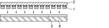
- FIGS. 1 and 2 show schematically a method of transferring the chip component and arranging it on the support tape in the step (1).
- step (1) as shown in FIG. 1, first, the surface on which the chip parts 1 of the member on which the chip parts 1 are arranged are arranged is placed on the curable pressure-sensitive adhesive layer of the support tape 3 having the curable pressure-sensitive adhesive layer. Paste to. That is, the back surface of the chip component 1 is bonded onto the curable adhesive layer of the support tape 3. Then, by removing the member 2 by a method such as peeling, the chip component 1 is transferred onto the curable adhesive layer of the support tape 3 as shown in FIG.
- the support tape 3 may be a single-sided tape or a double-sided tape, and may or may not have a base material. However, when the support tape 3 is a double-sided tape, the chip component 1 It is preferable that the surface opposite to the surface on which the transfer is transferred is attached to the support 4 such as glass.
- the member 2 is not particularly limited, and examples thereof include a glass substrate, a sapphire substrate, a silicon substrate, a metal substrate, and an organic substrate.
- the support 4 is not particularly limited, and examples thereof include a glass substrate, a sapphire substrate, a silicon substrate, a metal substrate, and an organic substrate.
- the chip component is not particularly limited, and examples thereof include a micro LED chip and an optical chip of an image sensor.
- the method for manufacturing an electronic component of the present invention is particularly effective for a very small chip member that does not have adhesive residue and is difficult to peel off with a good yield. Therefore, it is preferable that the chip component is a micro LED.
- the step (2) of irradiating an energy ray from a surface of the support tape on which the chip component is arranged is opposite to the surface on which the chip component is laminated is then performed.
- FIG. 3 shows a diagram schematically showing the state of the above step (2).
- energy rays are irradiated from the surface opposite to the surface on which the chip components of the support tape in which the chip components are arranged on the curable pressure-sensitive adhesive layer are laminated.
- the energy rays are not particularly limited as long as the curable pressure-sensitive adhesive layer can be cured, and examples thereof include ultrasonic waves and light. Above all, the energy ray is preferably light having a wavelength of 300 nm or more and 450 nm or less because it can be easily cured. Since the energy amount of the energy ray is sufficient to cure the curable pressure-sensitive adhesive layer, it is much smaller than the energy amount of the stimulus described later.
- the energy ray is light having a wavelength of 300 nm or more and 450 nm or less
- irradiate light having a wavelength of 365 nm with an integrated illuminance of 300 mJ / cm 2 or more and more preferably to irradiate with an integrated illuminance of 500 mJ / cm 2 or more and 10,000 mJ / cm 2 or less, 500 mJ / cm 2 or more. It is more preferable to irradiate with an integrated illuminance of 7500 mJ / cm 2 or less, and it is particularly preferable to irradiate with an integrated illuminance of 1000 mJ / cm 2 or more and 5000 mJ / cm 2 or less.
- a step (3) of transferring the chip component from the support tape to the next member is then performed by applying a stimulus from the surface of the support tape opposite to the surface on which the chip component is laminated.
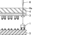
- FIG. 4 shows a diagram schematically showing the state of the above step (3).
- light irradiation is performed from the surface of the support tape 3 on which the chip component 1 is arranged, which is opposite to the surface on which the chip components are laminated, that is, the back surface of the support tape. Stimulation is applied by the light 6a emitted from the device 6.
- the molecules of the curable adhesive are broken by heat to reduce the molecular weight, and the molecules are momentarily evaporated or sublimated due to high temperature. Therefore, the light 6a of the support tape is irradiated. The part that has been burned out is burnt out. Therefore, by applying the above stimulus to the position on the chip component 1 of the support tape 3, the support tape is burnt out, the chip component 1 is peeled off from the support tape 3, and the chip component 1 is transferred onto the next member 5. .. At this time, since the curable adhesive layer of the support tape 3 is cured by the above step (2), the adhesive residue on the chip component 1 is unlikely to occur, and the chip component can be peeled off with a lighter force.
- the next member 5 is depicted as a substrate in FIG. 4, the next member 5 is not particularly limited, and for example, a glass substrate, a sapphire substrate, a silicon substrate, a metal substrate, an organic substrate, a drive circuit board, and the like. Adhesive tape and the like can be mentioned.
- the stimulus is not particularly limited as long as the chip component can be peeled off, and examples thereof include light, heat, electromagnetic waves, and electron beams.
- the stimulus is preferably a laser, more preferably a laser having a wavelength of 300 nm or more and 370 nm or less, and more preferably 350 nm or more, because even a very small chip member such as a micro LED can be peeled off individually and with good yield.
- a laser having a wavelength of 370 nm or less is more preferable. Since the amount of energy of the stimulus is such that the support tape can be burnt off, the amount of energy is much larger than the amount of energy of the energy rays.
- the stimulus may be applied to the entire support tape, or the stimulus may be applied to each chip component region to be peeled off from the support tape.
- the entire support tape it is preferable that a plurality of the chip components can be transferred at once, and when stimulating each region of the chip component to be peeled off from the support tape, the target chip component is intended. It is preferable in that only can be selectively transferred.
- the output of the laser is preferably 50 mJ / cm 2 or more and 1500 mJ / cm 2 or less at 5 nsec / pulse by pulse irradiation.
- the output of the laser is more preferably 100 mJ / cm 2 or more, and more preferably 1000 mJ / cm 2 or less.
- the curable pressure-sensitive adhesive layer contains a polymerizable polymer and a reaction initiator. Since the pressure-sensitive adhesive layer contains the polymerizable polymer and the reaction initiator, that is, the curable pressure-sensitive adhesive, the chip parts can be fixed with sufficient adhesive force in the above-mentioned step (1), and the above-mentioned step (1). By curing the curable pressure-sensitive adhesive layer in 2), the chip parts can be transferred without adhesive residue in the above step (3).
- reaction initiator is not particularly limited, and examples thereof include a photoreaction initiator, a thermal reaction initiator, and the like. Among them, light can be activated by irradiation with energy rays to cure the curable pressure-sensitive adhesive layer.
- a reaction initiator is preferable, and since it can also serve as an ultraviolet absorber described later, a photoreaction initiator using ultraviolet rays can be preferably used.
- a (meth) acrylic polymer having a functional group in the molecule (hereinafter referred to as a functional group-containing (meth) acrylic polymer) is synthesized in advance and reacted with the functional group in the molecule. It can be obtained by reacting a compound having a functional group to be subjected to a radically polymerizable unsaturated bond (hereinafter referred to as a functional group-containing unsaturated compound).
- (meth) acrylic means acrylic or methacrylic
- (meth) acrylate means acrylate or methacrylate.
- the functional group-containing (meth) acrylic polymer is, for example, an acrylic acid alkyl ester and / or a methacrylate alkyl ester in which the number of carbon atoms of the alkyl group is usually in the range of 2 to 18, a functional group-containing monomer, and further required. It can be obtained by copolymerizing these with other copolymerizable modifying monomers.
- the weight average molecular weight of the functional group-containing (meth) acrylic polymer is not particularly limited, but is usually about 200,000 to 2,000,000.
- the weight average molecular weight can be determined by using gel permeation chromatography. For example, HSPgelHR MB-M 6.0 ⁇ 150 mm as a column, THF as an eluent, measured at 40 ° C., and measured by a polystyrene standard. Can be decided.
- the functional group-containing monomer examples include a carboxyl group-containing monomer such as acrylic acid and methacrylic acid, a hydroxyl group-containing monomer such as hydroxyethyl acrylate and hydroxyethyl methacrylate, and an epoxy such as glycidyl acrylate and glycidyl methacrylate.
- Group-containing monomers can be mentioned.
- the functional group-containing monomer include isocyanate group-containing monomers such as ethyl isocyanate and ethyl methacrylate, and amino group-containing monomers such as aminoethyl acrylate and aminoethyl methacrylate.
- Examples of the other copolymerizable monomer for modification include various monomers used in general (meth) acrylic polymers such as vinyl acetate, acrylonitrile, and styrene.
- the raw material monomer may be subjected to a radical reaction in the presence of a polymerization initiator.
- a method of radically reacting the raw material monomer that is, a conventionally known method, a conventionally known method is used, and examples thereof include solution polymerization (boiling point polymerization or constant temperature polymerization), emulsion polymerization, suspension polymerization, bulk polymerization and the like.
- the polymerization initiator used in the radical reaction for obtaining the functional group-containing (meth) acrylic polymer is not particularly limited, and examples thereof include organic peroxides and azo compounds.
- organic peroxide examples include 1,1-bis (t-hexylperoxy) -3,3,5-trimethylcyclohexane, t-hexylperoxypivalate, t-butylperoxypivalate, 2,5. -Dimethyl-2,5-bis (2-ethylhexanoylperoxy) hexane, t-hexylperoxy-2-ethylhexanoate, t-butylperoxy-2-ethylhexanoate, t-butylperoxy Examples thereof include isobutyrate, t-butylperoxy-3,5,5-trimethylhexanoate, t-butylperoxylaurate and the like.
- the azo compound examples include azobisisobutyronitrile and azobiscyclohexanecarbonitrile. These polymerization initiators may be used alone or in combination of two or more.
- the functional group-containing unsaturated compound to be reacted with the functional group-containing (meth) acrylic polymer is the same as the above-mentioned functional group-containing monomer depending on the functional group of the functional group-containing (meth) acrylic polymer.
- the functional group of the functional group-containing (meth) acrylic polymer is a carboxyl group
- an epoxy group-containing monomer or an isocyanate group-containing monomer is used.
- the functional group of the functional group-containing (meth) acrylic polymer is a hydroxyl group
- an isocyanate group-containing monomer is used.
- the functional group of the functional group-containing (meth) acrylic polymer is an epoxy group
- a carboxyl group-containing monomer or an amide group-containing monomer such as acrylamide is used.
- the functional group of the functional group-containing (meth) acrylic polymer is an amino group
- an epoxy group-containing monomer is used.
- the curable pressure-sensitive adhesive layer may contain a radically polymerizable polyfunctional oligomer or monomer.
- a radically polymerizable polyfunctional oligomer or monomer By containing a radically polymerizable polyfunctional oligomer or monomer, the photocurability of the curable pressure-sensitive adhesive layer is improved.
- the polyfunctional oligomer or monomer is not particularly limited, but the weight average molecular weight is preferably 10,000 or less. Since the three-dimensional network of the curable pressure-sensitive adhesive layer is efficiently formed by light irradiation or heating, the polyfunctional oligomer or monomer has a weight average molecular weight of 5000 or less and a radically polymerizable unsaturated bond in the molecule.
- the number of radicals is preferably 2 to 20.
- polyfunctional oligomer or monomer examples include trimethylolpropane triacrylate, tetramethylolmethanetetraacrylate, pentaerythritol triacrylate, pentaerythritol tetraacrylate, dipentaerythritol monohydroxypentaacrylate, dipentaerythritol hexaacrylate, and the like. Examples include methacrylate. Examples of the polyfunctional oligomer or monomer include 1,4-butylene glycol diacrylate, 1,6-hexanediol diacrylate, polyethylene glycol diacrylate, commercially available oligoester acrylate, and methacrylates thereof. Be done. These polyfunctional oligomers or monomers may be used alone or in combination of two or more.
- the curable pressure-sensitive adhesive layer preferably contains an ultraviolet absorber.
- an ultraviolet absorber When the curable pressure-sensitive adhesive layer contains an ultraviolet absorber, it is possible to easily adjust the ultraviolet absorption rate, which will be described later, to a specific range. As a result, the chip parts can be peeled off without adhesive residue in the above step (3), and the yield can be further improved.
- the ultraviolet absorber is not particularly limited as long as it can absorb light having a wavelength of 200 nm to 400 nm. Further, the photoreaction initiator by ultraviolet rays is contained in the ultraviolet absorber at the same time as the reaction initiator.
- the curable pressure-sensitive adhesive layer preferably contains a photoreaction initiator by ultraviolet rays and an ultraviolet absorber other than the photoreaction initiator by ultraviolet rays.
- a photoreaction initiator by ultraviolet rays and an ultraviolet absorber other than the photoreaction initiator by ultraviolet rays.
- the ultraviolet-induced reaction initiator that remains unreacted during curing of the curable pressure-sensitive adhesive layer while acting as the above-mentioned reaction initiator is exposed to ultraviolet rays during peeling. It can also be used as an absorber.
- an ultraviolet absorber other than the photoreaction initiator in combination even if a large amount of the photoreaction initiator is consumed during the curing of the curable pressure-sensitive adhesive layer, the ultraviolet absorption property is lowered. It is possible to easily adjust the ultraviolet absorption rate after irradiation with energy rays, which will be described later, to a specific range.
- Examples of the ultraviolet-induced photoreaction initiator include those that are activated by irradiating light having a wavelength of 350 to 370 nm.
- Examples of such a photopolymerization initiator include acetophenone derivative compounds such as methoxyacetophenone, benzoin ether compounds such as benzoin propyl ether and benzoin isobutyl ether, ketal derivative compounds such as benzyl dimethyl ketal and acetophenone diethyl ketal, and the like.
- Examples include phosphine oxide derivative compounds.
- bis ( ⁇ 5-cyclopentadienyl) titanosen derivative compound benzophenone, Michler ketone, chlorothioxanthone, todecylthioxanthone, dimethylthioxanthone, diethylthioxanthone, ⁇ -hydroxycyclohexylphenylketone, 2-hydroxymethylphenylpropane and the like can also be mentioned.
- These ultraviolet photoreaction initiators may be used alone or in combination of two or more.
- the content of the photoreaction initiator by ultraviolet rays is preferably 1 part by weight or more with respect to 100 parts by weight of the polymerizable polymer.
- the content of the photoreaction initiator by ultraviolet rays with respect to 100 parts by weight of the polymerizable polymer is more preferably 2 parts by weight or more, further preferably 3 parts by weight or more.
- the upper limit of the content of the photoreaction initiator by ultraviolet rays with respect to 100 parts by weight of the polymerizable polymer is not particularly limited, but is preferably 10 parts by weight or less and 5 parts by weight or less, for example.
- the content of the photoreaction initiator by ultraviolet rays is preferably 50% by weight or less with respect to the total 100% by weight of the ultraviolet absorbers.
- the content of the photoreaction initiator by ultraviolet rays with respect to the total 100% by weight of the ultraviolet absorbers is more preferably 40% by weight or less, further preferably 30% by weight or less.
- the lower limit of the content of the photoreaction initiator by ultraviolet rays with respect to the total of the ultraviolet absorbers is not particularly limited, but is preferably, for example, 15% by weight.
- the ultraviolet absorber other than the photoreaction initiator by ultraviolet rays is not particularly limited, and for example, ethylhexyl methoxycinnamate, octyl methoxycinnamate, ethylhexyl paramethoxycinnamate, diethylaminohydroxybenzoyl, in addition to benzotriazole and hydroxylphenyltriazine.
- examples thereof include hexyl benzoate, bisethylhexyloxyphenol methoxyphenyltriazine, t-butylmethoxydibenzoylmethane and the like.
- benzotriazole-based and hydroxylphenyltriazine-based are preferable because they are excellent in compounding applicability to adhesives.
- the ultraviolet absorbers other than the above-mentioned ultraviolet-induced photoreaction initiator may be used alone or in combination of two or more.
- the total content of the ultraviolet absorber is preferably 6 parts by weight or more with respect to 100 parts by weight of the polymerizable polymer. By setting the total content of the ultraviolet absorber in the above range, the stimulus can be more efficiently converted into heat or vibration in the step (3), so that the chip component can be peeled off more reliably. ..
- the total content of the ultraviolet absorber is more preferably 10 parts by weight or more, further preferably 15 parts by weight or more.
- the upper limit of the total content of the ultraviolet absorber is not particularly limited, but is preferably 30 parts by weight or less from the viewpoint of ensuring the adhesive strength in the step (1).
- the curable pressure-sensitive adhesive layer may further contain an inorganic filler such as fumed silica.
- an inorganic filler such as fumed silica.
- the curable pressure-sensitive adhesive layer preferably contains a cross-linking agent.
- a cross-linking agent By containing the cross-linking agent, the cohesive force of the curable pressure-sensitive adhesive layer is increased, the adherend can be attached to the adherend with sufficient adhesive force, and the adherend can be sufficiently fixed.
- the above-mentioned cross-linking agent is not particularly limited, and examples thereof include an isocyanate-based cross-linking agent, an epoxy-based cross-linking agent, an aziridine-based cross-linking agent, and a metal chelate-based cross-linking agent. Of these, isocyanate-based cross-linking agents are preferable because they have higher adhesive strength.
- the content of the cross-linking agent is preferably 0.01 parts by weight or more and 20 parts by weight or less with respect to 100 parts by weight of the pressure-sensitive adhesive constituting the curable pressure-sensitive adhesive layer.
- the pressure-sensitive adhesive can be appropriately cross-linked to increase the adhesive strength.
- the more preferable lower limit of the content of the cross-linking agent is 0.05 parts by weight
- the more preferable upper limit is 15 parts by weight
- the further preferable lower limit is 0.1 parts by weight
- the further preferable upper limit is 10. It is a part by weight.
- the curable pressure-sensitive adhesive layer may contain known additives such as a plasticizer, a resin, a surfactant, a wax, and a fine particle filler. These additives may be used alone or in combination of two or more.
- the curable pressure-sensitive adhesive layer has an ultraviolet absorption rate of 95% or more at a wavelength of 365 nm before irradiation with energy rays. Since the ultraviolet absorption rate at the wavelength of 365 nm before the energy ray irradiation is within the above range, when a photoreaction initiator by ultraviolet rays is used as the ultraviolet absorber, the photoreaction initiator by ultraviolet rays when the curable pressure-sensitive adhesive layer is cured. Even when the ultraviolet rays are consumed, it is possible to maintain the ultraviolet absorption property to the extent that the chip parts can be easily peeled off without adhesive residue during the above step (3).
- the ultraviolet absorption rate at the wavelength of 365 nm before the energy ray irradiation is preferably 98% or more, more preferably 99% or more, and further preferably 99.5% or more.
- the upper limit of the ultraviolet absorption rate at the wavelength of 365 nm before the energy ray irradiation is not particularly limited, and the higher the upper limit, the better, but it is usually 100% or less.
- the ultraviolet absorption rate at the wavelength of 365 nm before the energy ray irradiation can be adjusted by using the type of the polymerizable polymer and the ultraviolet absorber.
- the ultraviolet absorption rate refers to the ultraviolet absorption rate of the curable pressure-sensitive adhesive layer in contact with the chip component.
- the ultraviolet absorption rate at the wavelength of 365 nm before the above energy ray irradiation is the absorption rate of ultraviolet rays at 365 nm (initial ultraviolet absorption) using an ultraviolet luminometer (UVPF-A2 manufactured by Eye Graphics Co., Ltd., or an equivalent product thereof) and a UV lamp. It can be obtained by measuring the rate).
- the UV lamp is adjusted so that the irradiation amount at a wavelength of 365 nm is 20 mw / cm 2 on one surface of the measurement sample.
- the amount of ultraviolet rays on the ultraviolet irradiation surface (before transmission) and the other surface (after transmission) of the measurement sample is measured with an ultraviolet luminometer, and the ultraviolet absorption rate is calculated from the following formula.
- the UV lamp is irradiated for 30 seconds for measurement.
- Ultraviolet ray absorption rate ⁇ (amount of ultraviolet rays before transmission)-(amount of ultraviolet rays after transmission) ⁇ / (amount of ultraviolet rays before transmission) ⁇ x 100 (%)
- the curable pressure-sensitive adhesive layer has an ultraviolet absorption rate of 95% or more at a wavelength of 365 nm after irradiation with energy rays.
- an adhesive that has not been burnt out by the laser may remain on the chip component, which causes defective products. Further, in the conventional method, the chip component may not be able to be peeled off unless the adhesive is completely burned out.
- the ultraviolet absorption rate at the wavelength of 365 nm after irradiation with energy rays within the above range, the stimulus in the above step (3) can be efficiently converted into heat or vibration, and the support tape can be burnt off more reliably.
- the ultraviolet absorption rate at the wavelength of 365 nm after the energy ray irradiation is preferably 96% or more, and more preferably 99% or more.
- the upper limit of the ultraviolet absorption rate at the wavelength of 365 nm before the energy ray irradiation is not particularly limited, and the higher the upper limit, the better, but it is usually 100% or less.
- the ultraviolet absorption rate at the wavelength of 365 nm after the energy ray irradiation can be adjusted by using the type of the polymerizable polymer and the ultraviolet absorber.
- the ultraviolet absorption rate at the wavelength of 365 nm after the energy ray irradiation is determined by irradiating the measurement sample with ultraviolet rays of 365 nm using an ultra-high pressure mercury ultraviolet ray irradiator so that the integrated irradiation amount becomes 3000 mJ / cm 2 . It can be obtained by performing the same measurement as the ultraviolet absorption rate at a wavelength of 365 nm before irradiation with energy rays.
- the curable pressure-sensitive adhesive layer preferably has a gel fraction of 20% by weight or more and 70% by weight or less before irradiation with energy rays.
- the gel fraction before irradiation with energy rays is within the above range, it can be attached to the adherend with sufficient adhesive force, and the adherend can be sufficiently fixed.
- the gel fraction of the curable pressure-sensitive adhesive layer is more preferably 30% by weight or more, and further preferably 60% by weight or less.
- the curable pressure-sensitive adhesive layer preferably has a gel fraction of 90% or more after irradiation with energy rays.
- the gel fraction after the energy ray irradiation is more preferably 93% or more, further preferably 95% or more.
- the upper limit of the gel fraction after irradiation with the energy rays is not particularly limited, but is preferably 99% or less from the viewpoint of suppressing unintentional peeling of chip parts.
- the gel fraction can be measured by the following method. Only the curable adhesive layer is scraped off from the support tape, weighed and immersed in 50 ml of ethyl acetate, and shaken with a shaker at a temperature of 23 ° C. and 200 rpm for 24 hours (hereinafter, scraped off).
- the pressure-sensitive adhesive layer is called a pressure-sensitive adhesive composition). After shaking, a metal mesh (opening # 200 mesh) is used to absorb ethyl acetate and ethyl acetate and separate the swollen pressure-sensitive adhesive composition.
- the separated pressure-sensitive adhesive composition is dried under the condition of 110 ° C. for 1 hour, and the weight of the pressure-sensitive adhesive composition containing the dried metal mesh is measured.
- the gel fraction of the curable pressure-sensitive adhesive layer is calculated using the following formula.
- Gel fraction (% by weight) 100 x (W1-W2) / W0 (W0: weight of initial pressure-sensitive adhesive composition, W1: weight of pressure-sensitive adhesive composition including dried metal mesh, W2: initial weight of metal mesh)
- the gel fraction after energy ray irradiation is determined by irradiating the base material side of the support tape with ultraviolet rays of 365 nm using an ultra-high pressure mercury ultraviolet ray irradiator so that the integrated irradiation amount becomes 3000 mJ / cm 2 . After the agent layer is cured, the gel fraction is measured.
- the curable pressure-sensitive adhesive layer preferably has a peeling force of 0.5 N / 25 mm or less after irradiation with energy rays.
- the peeling force of the curable pressure-sensitive adhesive layer after irradiation with energy rays is more preferably 0.3 N / 25 mm or less, and further preferably 0.2 N / 25 mm or less.
- the peeling force is 50 at 23 ° C.
- the thickness of the curable pressure-sensitive adhesive layer is not particularly limited, but is preferably 200 ⁇ m or less. When the thickness is 200 ⁇ m or less, the chip component can be peeled off while further suppressing the residue of the curable pressure-sensitive adhesive layer.
- a more preferable upper limit of the thickness is 50 ⁇ m, and a further preferable upper limit is 20 ⁇ m.
- the lower limit of the thickness is not particularly limited, but the preferable lower limit is 2 ⁇ m and the more preferable lower limit is 5 ⁇ m from the viewpoint of improving the peeling while holding the chip component.
- the support tape may be a single-sided adhesive tape or a double-sided adhesive tape.
- the support tape when a support is used, the support tape is preferably a double-sided adhesive tape because it can be easily attached to the support.
- the support tape when the support tape is a double-sided adhesive tape, the support tape may have at least one side of the curable adhesive layer, and the other side may be a curable adhesive layer but a non-curable adhesive layer. You may.
- a pressure-sensitive adhesive layer of the double-sided adhesive tape a pressure-sensitive adhesive having the same component may be used on both sides, or a pressure-sensitive adhesive having different components may be used.
- the double-sided adhesive tape preferably has an energy ray transmittance of 90% or more at 300 to 450 nm on the surface on which the chip component is not arranged.
- the energy ray transmittance of 300 to 450 nm on the surface where the chip parts of the double-sided adhesive tape are not arranged is more reliably cured during the step (2).
- the energy ray transmittance of 300 to 450 nm on the surface of the double-sided adhesive tape on which the chip component is not arranged is more preferably 95% or more.
- the support tape may be a support type having a base material or a non-support type having no base material, but the base material can be easily handled and cut. It is preferable to have.
- the substrate is not particularly limited, but the energy ray transmittance at 300 to 450 nm is preferably 90% or more, preferably 95%, from the viewpoint of more reliably curing the curable pressure-sensitive adhesive layer in the step (2). The above is more preferable.
- Examples of the material of the base material include polyethylene terephthalate, polyethylene naphthalate, polyacetal, polyamide, polycarbonate, polyphenylene ether, polybutylene terephthalate, ultrahigh molecular weight polyethylene, syndiotactic polystyrene, polyarylate, polysulfone, and polyether sulfone.
- Examples thereof include polyphenylene sulfide, polyether ether ketone, polyimide, polyetherimide, fluororesin, liquid crystal polymer and the like.
- polyethylene terephthalate and polyethylene naphthalate are preferable because they have excellent heat resistance.
- the thickness of the base material is not particularly limited, but a preferable lower limit is 5 ⁇ m and a preferable upper limit is 188 ⁇ m. When the thickness of the base material is within the above range, it is possible to obtain a support tape having an appropriate elasticity and excellent handleability. A more preferable lower limit of the thickness of the base material is 12 ⁇ m, and a more preferable upper limit is 125 ⁇ m.
- the application of the method for manufacturing an electronic component of the present invention is not particularly limited, and an electronic component using any chip component can be manufactured with a high yield, but the present invention is less likely to leave adhesive residue on the chip component. Since the chip component can be peeled off with a light force, it is particularly effective for extremely small chip components that do not have adhesive residue and are difficult to transfer with good yield. Therefore, the present invention is suitable for manufacturing a display device using a micro LED as a chip component.
- the step (2) of irradiating the energy rays from the surface opposite to the surface on which the micro LED chips are laminated, and the stimulation from the surface opposite to the surface on which the micro LED chips are laminated on the support tape are applied.
- the curing type pressure-sensitive adhesive layer comprises a step (3) of transferring a micro LED chip from a support tape to a next member, the curing type pressure-sensitive adhesive layer contains a polymerizable polymer and a reaction initiator, and the curing type pressure-sensitive adhesive layer is described above.
- the method for manufacturing a display device which has an ultraviolet absorption rate of 99% or more at a wavelength of 365 nm before energy ray irradiation and an ultraviolet absorption rate of 95% or more at a wavelength of 365 nm after the energy ray irradiation, is also according to the present invention.
- the details of the curable pressure-sensitive adhesive layer, the support tape, and each step the same method and method as those for manufacturing the above electronic components can be used.
- glue to a chip component and a micro LED chip is used by using a support tape having an ultraviolet absorption rate in a specific range at a wavelength of 365 nm before and after irradiation with energy rays. While suppressing the residue, the chip component and the micro LED chip can be more reliably peeled from the support tape, and the yield can be improved.
- a support tape having a curable pressure-sensitive adhesive layer on at least one surface the curable pressure-sensitive adhesive layer contains a polymerizable polymer and a reaction initiator, and the curable-type pressure-sensitive adhesive layer is an energy ray.
- a support tape having an ultraviolet absorption rate of 95% or more at a wavelength of 365 nm before irradiation and an ultraviolet absorption rate of 95% or more at a wavelength of 365 nm after the energy ray irradiation is also one of the present inventions.
- composition and structure of the polymerizable polymer, the reaction initiator and other components constituting the curable pressure-sensitive adhesive layer of the support tape of the present invention, the structure and structure of the support tape other than the curable pressure-sensitive adhesive layer, and the energy As for the method for measuring the ultraviolet absorption rate at the wavelength of 365 nm before beam irradiation and the ultraviolet absorption rate at the wavelength of 365 nm after the energy ray irradiation, the same method and method as the method for manufacturing the electronic component of the present invention can be used. ..
- the method for producing the support tape of the present invention is not particularly limited, and for example, the pressure-sensitive adhesive is obtained by adding the reaction initiator and other additives such as an ultraviolet absorber as necessary to the solution of the polymerizable polymer and mixing them.
- the pressure-sensitive adhesive is obtained by adding the reaction initiator and other additives such as an ultraviolet absorber as necessary to the solution of the polymerizable polymer and mixing them.
- a non-support type support tape composed of a curable pressure-sensitive adhesive layer can be manufactured.
- a support type single-sided or double-sided support tape can also be manufactured by adhering the curable pressure-sensitive adhesive layer produced by the above method to a base material or applying the pressure-sensitive adhesive solution to the base material and drying the base material.
- a method for manufacturing an electronic component capable of suppressing adhesive residue on a chip component and transferring the chip component with a high yield a method for manufacturing a display device using the method for manufacturing the electronic component, and a method for manufacturing a display device.
- the support tape used in the manufacturing method can be provided.
- an ethyl acetate solution of a functional group-containing (meth) acrylic polymer having a solid content of 55% by weight and a weight average molecular weight of 600,000 was obtained.
- 12 parts by weight of 2-isocyanatoethyl methacrylate was added and reacted to cause a reaction (meth) acrylic polymer (meth).
- a solution of ethyl acetate (polymerizable polymer) was obtained.
- Example 1 Manufacturing of support tape 1 1.25 parts by weight of a cross-linking agent (Esdyne curing agent UA, manufactured by Sekisui Fuller) and a photoreaction initiator (with respect to 100 parts by weight of the resin solid content (polymerizable polymer) of the obtained ethyl acetate solution of the polymerizable polymer). 1 part by weight of a photoreaction initiator by ultraviolet rays, Omnirad651, manufactured by Toyotsukemi Plus Co., Ltd., and 5 parts by weight of an ultraviolet absorber (Tinuvin 928, manufactured by Fujifilm Wako Pure Chemical Industries, Ltd.) were mixed.
- a cross-linking agent Esdyne curing agent UA, manufactured by Sekisui Fuller
- a photoreaction initiator with respect to 100 parts by weight of the resin solid content (polymerizable polymer) of the obtained ethyl acetate solution of the polymerizable polymer.
- an ethyl acetate solution of the curable pressure-sensitive adhesive was obtained.
- the obtained curable pressure-sensitive adhesive solution was applied on a corona-treated PET film (base material) having a thickness of 50 ⁇ m with a doctor knife so that the thickness of the dry film was 20 ⁇ m, and the mixture was applied at room temperature for 10 minutes. It was left still.
- the coating solution was dried by heating at 110 ° C. for 5 minutes using an oven preheated to 110 ° C. to obtain a support tape having a curable pressure-sensitive adhesive layer and a base material.
- the support tape side of another measurement sample prepared by the same method was irradiated with ultraviolet rays of 365 nm using an ultrahigh pressure mercury ultraviolet irradiation device so that the integrated irradiation amount was 3000 mJ / cm 2 .
- the illuminance was adjusted so that the irradiation intensity was 100 mW / cm 2 .
- a peeling test was conducted by the same method as the initial peeling force, and the peeling force after irradiation with energy rays was measured. The results are shown in Table 1.
- UV Absorption Rate A measurement sample of only the curable pressure-sensitive adhesive layer was prepared by the above method. With respect to the obtained measurement sample, the absorption rate of ultraviolet rays at 365 nm (initial ultraviolet absorption rate) was measured by the following method using an ultraviolet luminometer (UVPF-A2 manufactured by Eye Graphics Co., Ltd.) and a UV lamp. The UV lamp was adjusted so that the irradiation amount at a wavelength of 365 nm was 20 mw / cm 2 on one surface of the measurement sample. The amount of ultraviolet rays on the ultraviolet-irradiated surface (before transmission) and the other surface (after transmission) of the measurement sample was measured with an ultraviolet luminometer, and the ultraviolet absorption rate was calculated from the following formula.
- UV luminometer UVPF-A2 manufactured by Eye Graphics Co., Ltd.
- the UV lamp was irradiated for 30 seconds and measured.
- Ultraviolet ray absorption rate ⁇ (amount of ultraviolet rays before transmission)-(amount of ultraviolet rays after transmission) ⁇ / (amount of ultraviolet rays before transmission) ⁇ x 100 (%)
- the measurement sample was irradiated with ultraviolet rays of 365 nm using an ultrahigh pressure mercury ultraviolet irradiation device so that the integrated irradiation amount was 3000 mJ / cm 2 .
- the absorption rate of ultraviolet rays at 365 nm (ultraviolet absorption rate after irradiation with energy rays) was measured by the same method. The results are shown in Table 1.
- the obtained support tape was cut into 200 mm ⁇ 200 mm.
- the curable pressure-sensitive adhesive layer was cured by irradiating the base material side of the cut support tape with ultraviolet rays of 365 nm using an ultra-high pressure mercury ultraviolet irradiation device so that the integrated irradiation amount was 3000 mJ / cm 2 .
- the scraped adhesive layer is referred to as an adhesive composition.
- a metal mesh (opening # 200 mesh) was used to absorb ethyl acetate and ethyl acetate, and the swollen pressure-sensitive adhesive composition was separated.
- the separated pressure-sensitive adhesive composition was dried under the condition of 110 ° C. for 1 hour.
- the weight of the pressure-sensitive adhesive composition containing the dried metal mesh was measured, and the gel fraction of the curable pressure-sensitive adhesive layer after energy ray irradiation was calculated using the following formula. The results are shown in Table 1.
- Gel fraction (% by weight) 100 x (W1-W2) / W0 (W0: weight of initial pressure-sensitive adhesive composition, W1: weight of pressure-sensitive adhesive composition including dried metal mesh, W2: initial weight of metal mesh)
- Examples 2 to 6 Comparative Examples 1 and 2
- a support tape was obtained in the same manner as in Example 1 except that the blending amounts of the photoreaction initiator and the ultraviolet absorber were as shown in Table 1, and each measurement was carried out. The results are shown in Table 1.
- Example 7 Manufacturing of support tape 2
- a cross-linking agent Esdyne curing agent UA, manufactured by Sekisui Fuller
- a photoreaction initiator with respect to 100 parts by weight of the resin solid content (polymerizable polymer) of the obtained ethyl acetate solution of the polymerizable polymer.
- an ethyl acetate solution of the curable pressure-sensitive adhesive was obtained.
- the obtained curable pressure-sensitive adhesive solution was applied on a corona-treated PET film (base material) having a thickness of 50 ⁇ m with a doctor knife so that the thickness of the dry film was 20 ⁇ m, and the mixture was applied at room temperature for 10 minutes. It was left still.
- the coating solution was dried by heating at 110 ° C. for 5 minutes using an oven preheated to 110 ° C. to obtain a support tape having a curable pressure-sensitive adhesive layer and a base material. Each measurement was carried out on the obtained support tape in the same manner as in Example 1. The results are shown in Table 1.
- the Si chip is separated by adhering the Si chip side surface of the wafer in which 10 Si chips (500 ⁇ m ⁇ 500 ⁇ m square, thickness 50 ⁇ m) are arranged to the curable adhesive layer side of the support tape, and then peeling off the wafer. Transferred onto the instruction tape.
- a high-pressure mercury ultraviolet irradiation device (GWSM-300R, manufactured by Takatori Co., Ltd.) is used to irradiate 365 nm ultraviolet rays from the base material side of the support tape so that the integrated irradiation amount is 3000 mJ / cm 2 .
- the agent layer was cured.
- each Si chip was irradiated with a laser having an output of 4 W and 4 KHz at 365 nm from the base material side of the support tape, and the Si chip was peeled off from the support tape.
- a method for manufacturing an electronic component capable of suppressing adhesive residue on a chip component and transferring the chip component with a high yield a method for manufacturing a display device using the method for manufacturing the electronic component, and a method for manufacturing a display device.
- the support tape used in the manufacturing method can be provided.
- Chip part 2 Member 3 Support tape 4 Support 5th member 6 Light irradiation device 6a Light
Landscapes
- Chemical & Material Sciences (AREA)
- Organic Chemistry (AREA)
- Adhesives Or Adhesive Processes (AREA)
- Devices For Indicating Variable Information By Combining Individual Elements (AREA)
- Adhesive Tapes (AREA)
- Wire Bonding (AREA)
- Container, Conveyance, Adherence, Positioning, Of Wafer (AREA)
- Led Device Packages (AREA)
- Dicing (AREA)
Abstract
本発明は、チップ部品への糊残りを抑制し、かつ、チップ部品を歩留まりよく転写することができる電子部品の製造方法、該電子部品の製造方法を用いた表示装置の製造方法、及び、該製造方法に用いられる支持テープを提供することを目的とする。本発明は、少なくとも1つの表面に硬化型粘着剤層を有する支持テープの前記硬化型粘着剤層上にチップ部品を配置する工程(1)と、前記チップ部品が配置された前記支持テープの前記チップ部品が積層した面とは反対側の面よりエネルギー線を照射する工程(2)と、前記支持テープの前記チップ部品が積層した面とは反対側の面より刺激を加え、チップ部品を支持テープから次部材へ転写する工程(3)とを有し、前記硬化型粘着剤層は重合性ポリマーと反応開始剤とを含有し、前記硬化型粘着剤層は、前記エネルギー線照射前の365nmの波長における紫外線吸収率が95%以上であり、前記エネルギー線照射後の365nmの波長における紫外線吸収率が95%以上である、電子部品の製造方法である。
Description
本発明は、電子部品の製造方法、表示装置の製造方法、及び、該製造方法に用いられる支持テープに関する。
マイクロLEDディスプレイは、画素を構成するチップの1つ1つが微細な発光ダイオード(LED、Light Emitting Diode)チップであり、このマイクロLEDチップが自発光して画像を表示する表示装置である。マイクロLEDディスプレイは、コントラストが高く、応答速度が速く、また、液晶ディスプレイ、有機ELディスプレイ等で使用されるカラーフィルターを必要としないこと等により薄型化も可能であることから、次世代の表示装置として注目されている。
マイクロLEDディスプレイにおいては、多数のマイクロLEDチップが平面状に高密度で敷き詰められている。このようなマイクロLEDディスプレイを製造する際には、粘着剤層を有する転写用基板上に多数のマイクロLEDチップが配置された転写用積層体から、駆動回路基板上にマイクロLEDチップを転写し、電気的に接続する工程が行われる。
マイクロLEDチップの転写工程では、転写用積層体のLEDチップが配置された面と、駆動回路基板の電極が形成された面とを対向させた状態で、転写用積層体からマイクロLEDチップを剥離させて転写する。
マイクロLEDチップの転写工程では、転写用積層体のLEDチップが配置された面と、駆動回路基板の電極が形成された面とを対向させた状態で、転写用積層体からマイクロLEDチップを剥離させて転写する。
転写用積層体からマイクロLEDチップを剥離させる方法としては、例えば、転写用積層体の基板の背面から粘着剤層に焦点をあててレーザー光を照射することで、マイクロLEDチップを剥離させる方法が知られている(例えば、特許文献1)。また、熱膨張性粒子、熱膨張性マイクロカプセル等を配合した粘着剤層を用い、転写用積層体と駆動回路基板とを熱圧着して熱膨張性粒子、熱膨張性マイクロカプセル等を熱膨張させることで、粘着剤層を変形させ、接着面積を低下させてマイクロLEDチップを剥離させる方法も知られている(例えば、特許文献2、3)。
しかしながら、特許文献1~3に記載のようなレーザー光を照射する方法又は熱膨張性粒子、熱膨張性マイクロカプセル等を用いる方法では、マイクロLEDチップに粘着剤層の残渣が付着するという問題がある。また、従来のレーザー光を照射する方法では、剥離不良によってマイクロLEDチップを剥離できないことがあり、歩留まりよくマイクロLEDチップを転写することが難しかった。
本発明は、チップ部品への糊残りを抑制し、かつ、チップ部品を歩留まりよく転写することができる電子部品の製造方法、該電子部品の製造方法を用いた表示装置の製造方法、及び、該製造方法に用いられる支持テープを提供することを目的とする。
本発明は、少なくとも1つの表面に硬化型粘着剤層を有する支持テープの前記硬化型粘着剤層上にチップ部品を配置する工程(1)と、前記チップ部品が配置された前記支持テープの前記チップ部品が積層した面とは反対側の面よりエネルギー線を照射する工程(2)と、前記支持テープの前記チップ部品が積層した面とは反対側の面より刺激を加え、チップ部品を支持テープから次部材へ転写する工程(3)とを有し、前記硬化型粘着剤層は重合性ポリマーと反応開始剤とを含有し、前記硬化型粘着剤層は、前記エネルギー線照射前の365nmの波長における紫外線吸収率が95%以上であり、前記エネルギー線照射後の365nmの波長における紫外線吸収率が95%以上である、電子部品の製造方法である。
以下に本発明を詳述する。
以下に本発明を詳述する。
本発明の電子部品の製造方法は、まず、少なくとも1つの表面に硬化型粘着剤層を有する支持テープの上記硬化型粘着剤層上にチップ部品を配置する工程(1)を行う。
上記工程(1)の具体的な方法は特に限定されず、例えば、各チップ部品を個別に支持テープ上に配置する方法や、支持テープにウエハを貼り付けて個片化する方法や、基板や粘着テープ等の部材上に配置されたチップ部品を支持テープ上に転写する方法等が挙げられる。なかでも、生産効率に優れることから、部材上に配置されたチップ部品を支持テープ上に転写する方法が好ましい。より具体的には、上記工程(1)は、上記チップ部品を配置した部材の上記チップ部品側の面と上記支持テープとを貼り合わせ、上記部材を除去することで、上記支持テープの上記硬化型粘着剤層上にチップ部品を配置する工程であることが好ましい。
上記工程(1)の具体的な方法は特に限定されず、例えば、各チップ部品を個別に支持テープ上に配置する方法や、支持テープにウエハを貼り付けて個片化する方法や、基板や粘着テープ等の部材上に配置されたチップ部品を支持テープ上に転写する方法等が挙げられる。なかでも、生産効率に優れることから、部材上に配置されたチップ部品を支持テープ上に転写する方法が好ましい。より具体的には、上記工程(1)は、上記チップ部品を配置した部材の上記チップ部品側の面と上記支持テープとを貼り合わせ、上記部材を除去することで、上記支持テープの上記硬化型粘着剤層上にチップ部品を配置する工程であることが好ましい。
ここで、上記工程(1)のなかでも上記チップ部品を転写して支持テープ上に配置する方法の様子を模式的に表した図を図1、2に示す。上記工程(1)では、図1に示すように、まずチップ部品1を配置した部材のチップ部品1が配列された面を、硬化型粘着剤層を有する支持テープ3の硬化型粘着剤層上に貼り合わせる。即ち、チップ部品1の背面を、支持テープ3の硬化型粘着剤層上へ貼り合わせる。その後、部材2を剥離等の方法で除去することで、図2に示すように、チップ部品1が支持テープ3の硬化型粘着剤層上へ転写される。上記支持テープ3は片面テープであっても両面テープであってもよいし、基材を有していてもいなくてもよいが、上記支持テープ3が両面テープである場合は、上記チップ部品1を転写する面とは反対側の面はガラス等の支持体4に貼り付けられることが好ましい。上記部材2は特に限定されず、例えば、ガラス基板、サファイヤ基板、シリコン基板、金属基板、有機基板等が挙げられる。
上記支持体4は特に限定されず、例えば、ガラス基板、サファイヤ基板、シリコン基板、金属基板、有機基板等が挙げられる。
上記支持体4は特に限定されず、例えば、ガラス基板、サファイヤ基板、シリコン基板、金属基板、有機基板等が挙げられる。
上記チップ部品は特に限定されず、例えば、マイクロLEDチップ、イメージセンサーの光学チップ等が挙げられる。なかでも、本発明の電子部品の製造方法は、糊残りなく、かつ、歩留まりよく剥離することが難しい極小のチップ部材において特に効果が高いことから、上記チップ部品がマイクロLEDであることが好ましい。
本発明の電子部品の製造方法は、次いで、上記チップ部品が配置された上記支持テープの上記チップ部品が積層した面とは反対側の面よりエネルギー線を照射する工程(2)を行う。
ここで、上記工程(2)の様子を模式的に表した図を図3に示す。図3に示すように、上記工程(2)では硬化型粘着剤層上にチップ部品が配置された支持テープのチップ部品が積層した面とは反対側の面よりエネルギー線を照射する。エネルギー線を照射することにより支持テープ3の硬化型粘着剤層が硬化するため、支持テープ3の粘着力が低下し、チップ部品1への糊残りを抑えつつチップ部品1を剥離することが可能になる。また、糊残りのない正常なチップを転写できることから、不良品の数を減らすことができ、歩留まりを向上させることができる。
上記エネルギー線は上記硬化型粘着剤層を硬化させることができれば特に限定されず、例えば、超音波、光等が挙げられる。なかでも、硬化が容易に行えることから、上記エネルギー線は300nm以上450nm以下の波長の光であることが好ましい。なお、上記エネルギー線のエネルギー量は、上記硬化型粘着剤層を硬化できる程度であるため、後述する刺激のエネルギー量と比べて格段に小さいものである。
ここで、上記工程(2)の様子を模式的に表した図を図3に示す。図3に示すように、上記工程(2)では硬化型粘着剤層上にチップ部品が配置された支持テープのチップ部品が積層した面とは反対側の面よりエネルギー線を照射する。エネルギー線を照射することにより支持テープ3の硬化型粘着剤層が硬化するため、支持テープ3の粘着力が低下し、チップ部品1への糊残りを抑えつつチップ部品1を剥離することが可能になる。また、糊残りのない正常なチップを転写できることから、不良品の数を減らすことができ、歩留まりを向上させることができる。
上記エネルギー線は上記硬化型粘着剤層を硬化させることができれば特に限定されず、例えば、超音波、光等が挙げられる。なかでも、硬化が容易に行えることから、上記エネルギー線は300nm以上450nm以下の波長の光であることが好ましい。なお、上記エネルギー線のエネルギー量は、上記硬化型粘着剤層を硬化できる程度であるため、後述する刺激のエネルギー量と比べて格段に小さいものである。
上記エネルギー線が300nm以上450nm以下の波長の光である場合、上記工程(2)では、波長365nmの光を5mW/cm2以上の照度で照射することが好ましく、10mW/cm2以上の照度で照射することがより好ましく、20mW/cm2以上の照度で照射することが更に好ましく、50mW/cm2以上の照度で照射することが特に好ましい。また、波長365nmの光を300mJ/cm2以上の積算照度で照射することが好ましく、500mJ/cm2以上、10000mJ/cm2以下の積算照度で照射することがより好ましく、500mJ/cm2以上、7500mJ/cm2以下の積算照度で照射することが更に好ましく、1000mJ/cm2以上、5000mJ/cm2以下の積算照度で照射することが特に好ましい。
本発明の電子部品の製造方法は、次いで、上記支持テープの上記チップ部品が積層した面とは反対側の面より刺激を加え、チップ部品を支持テープから次部材へ転写する工程(3)を行う。
ここで、上記工程(3)の様子を模式的に表した図を図4に示す。図4に示すように、上記工程(3)では、チップ部品1が配置された支持テープ3の、チップ部品が積層した面とは反対側の面、つまり、支持テープの背面から、例えば光照射装置6から照射される光6aにより刺激を加える。上記刺激を支持テープ3に加えると、熱によって硬化型粘着剤の分子が切れて低分子化し、瞬間的に蒸発したり、高温となることで昇華したりするため、支持テープの光6aを照射した部分が焼き切れる。従って、上記刺激を支持テープ3のチップ部品1上の位置に加えることで、支持テープが焼き切れ、支持テープ3からチップ部品1が剥離して、次部材5上にチップ部品1が転写される。この際、上記工程(2)によって支持テープ3の硬化型粘着剤層は硬化しているため、チップ部品1への糊残りが起き難く、より軽い力でチップ部品を剥離できる。その結果、糊残りが起き難く、チップ部品を転写することができるため、歩留まりを向上させることができる。また、上記刺激によりチップ部品を剥離する方法は、ごく小さい範囲に対して剥離を起こさせることができるため、マイクロLEDのような極小のチップ部品が配列している場合であっても個別かつ歩留まりよく剥離することができる。更に、後述するが、上記支持テープ3の硬化型粘着剤層は特定波長の紫外線の吸収率が高く、上記刺激を効率よく熱や振動に変えることができるため、支持テープをよりムラなく確実に焼き切ることができ、更に糊残りを抑えられるとともに剥離不良を抑えることもできる。なお、図4では次部材5を基板として描写しているが、上記次部材5は、特に限定されず、例えば、ガラス基板、サファイヤ基板、シリコン基板、金属基板、有機基板や、駆動回路基板、粘着テープ等が挙げられる。
ここで、上記工程(3)の様子を模式的に表した図を図4に示す。図4に示すように、上記工程(3)では、チップ部品1が配置された支持テープ3の、チップ部品が積層した面とは反対側の面、つまり、支持テープの背面から、例えば光照射装置6から照射される光6aにより刺激を加える。上記刺激を支持テープ3に加えると、熱によって硬化型粘着剤の分子が切れて低分子化し、瞬間的に蒸発したり、高温となることで昇華したりするため、支持テープの光6aを照射した部分が焼き切れる。従って、上記刺激を支持テープ3のチップ部品1上の位置に加えることで、支持テープが焼き切れ、支持テープ3からチップ部品1が剥離して、次部材5上にチップ部品1が転写される。この際、上記工程(2)によって支持テープ3の硬化型粘着剤層は硬化しているため、チップ部品1への糊残りが起き難く、より軽い力でチップ部品を剥離できる。その結果、糊残りが起き難く、チップ部品を転写することができるため、歩留まりを向上させることができる。また、上記刺激によりチップ部品を剥離する方法は、ごく小さい範囲に対して剥離を起こさせることができるため、マイクロLEDのような極小のチップ部品が配列している場合であっても個別かつ歩留まりよく剥離することができる。更に、後述するが、上記支持テープ3の硬化型粘着剤層は特定波長の紫外線の吸収率が高く、上記刺激を効率よく熱や振動に変えることができるため、支持テープをよりムラなく確実に焼き切ることができ、更に糊残りを抑えられるとともに剥離不良を抑えることもできる。なお、図4では次部材5を基板として描写しているが、上記次部材5は、特に限定されず、例えば、ガラス基板、サファイヤ基板、シリコン基板、金属基板、有機基板や、駆動回路基板、粘着テープ等が挙げられる。
上記刺激は、上記チップ部品を剥離することができれば特に限定されず、例えば、光、熱、電磁波又は電子線等が挙げられる。なかでも、マイクロLED等の極小のチップ部材であっても個別かつ歩留まりよく剥離できることから、上記刺激はレーザーであることが好ましく、300nm以上370nm以下の波長のレーザーであることがより好ましく、350nm以上370nm以下の波長のレーザーであることが更に好ましい。なお、上記刺激のエネルギー量は、支持テープを焼き切ることができる程度であるため、上記エネルギー線のエネルギー量よりも格段に大きいものである。
上記工程(3)では支持テープ全体に対して上記刺激を加えてもよいし、上記支持テープの剥離させるチップ部品領域ごとに刺激を加えてもよい。上記支持テープ全体に対して刺激を加える場合は、複数の上記チップ部品を一挙に転写できる点で好ましく、上記支持テープの剥離させるチップ部品領域ごとに刺激を加える場合は、目的とする上記チップ部品のみを選択的に転写できる点で好ましい。
上記刺激がレーザーである場合、上記レーザーの出力はパルス照射により、5nsec/パルスで50mJ/cm2以上1500mJ/cm2以下であることが好ましい。
レーザーの出力を上記範囲とすることで、目標のチップ部品上の支持テープのみを充分に焼き切ることができ、より糊残りなく確実にチップ部品を剥離することができる。また、目的とする上記チップ部品のみを選択的に転写することが容易となる。上記レーザーの出力は100mJ/cm2以上であることがより好ましく、1000mJ/cm2以下であることがより好ましい。
レーザーの出力を上記範囲とすることで、目標のチップ部品上の支持テープのみを充分に焼き切ることができ、より糊残りなく確実にチップ部品を剥離することができる。また、目的とする上記チップ部品のみを選択的に転写することが容易となる。上記レーザーの出力は100mJ/cm2以上であることがより好ましく、1000mJ/cm2以下であることがより好ましい。
上記硬化型粘着剤層は重合性ポリマーと反応開始剤とを含有する。
粘着剤層が重合性ポリマーと反応開始剤を含有する、つまり、硬化型粘着剤を含有することで、上記工程(1)では充分な粘着力でチップ部品を固定することができ、上記工程(2)で硬化型粘着剤層を硬化させることにより、上記工程(3)で糊残りなくチップ部品を転写することができる。
粘着剤層が重合性ポリマーと反応開始剤を含有する、つまり、硬化型粘着剤を含有することで、上記工程(1)では充分な粘着力でチップ部品を固定することができ、上記工程(2)で硬化型粘着剤層を硬化させることにより、上記工程(3)で糊残りなくチップ部品を転写することができる。
上記反応開始剤は特に限定されず、例えば、光反応開始剤、熱反応開始剤等が挙げられ、なかでも、エネルギー線照射により活性化し、硬化型粘着剤層を硬化することができるため、光反応開始剤が好ましく、後述の紫外線吸収剤としての役割も果たせることから、紫外線による光反応開始剤を好適に用いることができる。
上記重合性ポリマーは、例えば、分子内に官能基を持った(メタ)アクリル系ポリマー(以下、官能基含有(メタ)アクリル系ポリマーという)を予め合成し、分子内に上記の官能基と反応する官能基とラジカル重合性の不飽和結合とを有する化合物(以下、官能基含有不飽和化合物という)を反応させることにより得ることができる。なお、(メタ)アクリルとは、アクリル又はメタクリルを意味し、(メタ)アクリレートとは、アクリレート又はメタクリレートを意味する
上記官能基含有(メタ)アクリル系ポリマーは、例えば、アルキル基の炭素数が通常2~18の範囲にあるアクリル酸アルキルエステル及び/又はメタクリル酸アルキルエステルと、官能基含有モノマーと、更に必要に応じてこれらと共重合可能な他の改質用モノマーとを共重合させることにより得ることができる。
上記官能基含有(メタ)アクリル系ポリマーの重量平均分子量は特に限定されないが、通常、20万~200万程度である。
なお、重量平均分子量は、ゲルパーミエーションクロマトグラフィを用いて決定することができ、例えば、カラムとしてHSPgelHR MB-M 6.0×150mm、溶出液としてTHFを用い、40℃で測定し、ポリスチレン標準により決定することができる。
なお、重量平均分子量は、ゲルパーミエーションクロマトグラフィを用いて決定することができ、例えば、カラムとしてHSPgelHR MB-M 6.0×150mm、溶出液としてTHFを用い、40℃で測定し、ポリスチレン標準により決定することができる。
上記官能基含有モノマーとしては、例えば、アクリル酸、メタクリル酸等のカルボキシル基含有モノマーや、アクリル酸ヒドロキシエチル、メタクリル酸ヒドロキシエチル等のヒドロキシル基含有モノマーや、アクリル酸グリシジル、メタクリル酸グリシジル等のエポキシ基含有モノマーが挙げられる。また、上記官能基含有モノマーとしては、例えば、アクリル酸イソシアネートエチル、メタクリル酸イソシアネートエチル等のイソシアネート基含有モノマーや、アクリル酸アミノエチル、メタクリル酸アミノエチル等のアミノ基含有モノマー等も挙げられる。
上記共重合可能な他の改質用モノマーとしては、例えば、酢酸ビニル、アクリロニトリル、スチレン等の一般の(メタ)アクリル系ポリマーに用いられている各種のモノマーが挙げられる。
上記官能基含有(メタ)アクリル系ポリマーを得るには、原料モノマーを、重合開始剤の存在下にてラジカル反応させればよい。上記原料モノマーをラジカル反応させる方法、即ち、重合方法としては、従来公知の方法が用いられ、例えば、溶液重合(沸点重合又は定温重合)、乳化重合、懸濁重合、塊状重合等が挙げられる。
上記官能基含有(メタ)アクリル系ポリマーを得るためのラジカル反応に用いる重合開始剤は特に限定されず、例えば、有機過酸化物、アゾ化合物等が挙げられる。上記有機過酸化物として、例えば、1,1-ビス(t-ヘキシルパーオキシ)-3,3,5-トリメチルシクロヘキサン、t-ヘキシルパーオキシピバレート、t-ブチルパーオキシピバレート、2,5-ジメチル-2,5-ビス(2-エチルヘキサノイルパーオキシ)ヘキサン、t-ヘキシルパーオキシ-2-エチルヘキサノエート、t-ブチルパーオキシ-2-エチルヘキサノエート、t-ブチルパーオキシイソブチレート、t-ブチルパーオキシ-3,5,5-トリメチルヘキサノエート、t-ブチルパーオキシラウレート等が挙げられる。上記アゾ化合物として、例えば、アゾビスイソブチロニトリル、アゾビスシクロヘキサンカルボニトリル等が挙げられる。これらの重合開始剤は単独で用いられてもよく、2種以上が併用されてもよい。
上記官能基含有(メタ)アクリル系ポリマーを得るためのラジカル反応に用いる重合開始剤は特に限定されず、例えば、有機過酸化物、アゾ化合物等が挙げられる。上記有機過酸化物として、例えば、1,1-ビス(t-ヘキシルパーオキシ)-3,3,5-トリメチルシクロヘキサン、t-ヘキシルパーオキシピバレート、t-ブチルパーオキシピバレート、2,5-ジメチル-2,5-ビス(2-エチルヘキサノイルパーオキシ)ヘキサン、t-ヘキシルパーオキシ-2-エチルヘキサノエート、t-ブチルパーオキシ-2-エチルヘキサノエート、t-ブチルパーオキシイソブチレート、t-ブチルパーオキシ-3,5,5-トリメチルヘキサノエート、t-ブチルパーオキシラウレート等が挙げられる。上記アゾ化合物として、例えば、アゾビスイソブチロニトリル、アゾビスシクロヘキサンカルボニトリル等が挙げられる。これらの重合開始剤は単独で用いられてもよく、2種以上が併用されてもよい。
上記官能基含有(メタ)アクリル系ポリマーに反応させる官能基含有不飽和化合物としては、上記官能基含有(メタ)アクリル系ポリマーの官能基に応じて、上述した官能基含有モノマーと同様のものを使用できる。例えば、上記官能基含有(メタ)アクリル系ポリマーの官能基がカルボキシル基の場合は、エポキシ基含有モノマーやイソシアネート基含有モノマーが用いられる。上記官能基含有(メタ)アクリル系ポリマーの官能基がヒドロキシル基の場合は、イソシアネート基含有モノマーが用いられる。上記官能基含有(メタ)アクリル系ポリマーの官能基がエポキシ基の場合は、カルボキシル基含有モノマーやアクリルアミド等のアミド基含有モノマーが用いられる。上記官能基含有(メタ)アクリル系ポリマーの官能基がアミノ基の場合は、エポキシ基含有モノマーが用いられる。
上記硬化型粘着剤層は、ラジカル重合性の多官能オリゴマー又はモノマーを含有していてもよい。ラジカル重合性の多官能オリゴマー又はモノマーを含有することにより、上記硬化型粘着剤層の光硬化性が向上する。
上記多官能オリゴマー又はモノマーは特に限定されないが、重量平均分子量が1万以下であることが好ましい。光照射又は加熱による上記硬化型粘着剤層の三次元網状化が効率よくなされることから、上記多官能オリゴマー又はモノマーは、重量平均分子量が5000以下でかつ分子内のラジカル重合性の不飽和結合の数が2~20個であることが好ましい。
上記多官能オリゴマー又はモノマーは特に限定されないが、重量平均分子量が1万以下であることが好ましい。光照射又は加熱による上記硬化型粘着剤層の三次元網状化が効率よくなされることから、上記多官能オリゴマー又はモノマーは、重量平均分子量が5000以下でかつ分子内のラジカル重合性の不飽和結合の数が2~20個であることが好ましい。
上記多官能オリゴマー又はモノマーとして、例えば、トリメチロールプロパントリアクリレート、テトラメチロールメタンテトラアクリレート、ペンタエリスリトールトリアクリレート、ペンタエリスリトールテトラアクリレート、ジペンタエリスリトールモノヒドロキシペンタアクリレート、ジペンタエリスリトールヘキサアクリレート、及び、これらのメタクリレート等が挙げられる。また、上記多官能オリゴマー又はモノマーとしては、例えば、1,4-ブチレングリコールジアクリレート、1,6-ヘキサンジオールジアクリレート、ポリエチレングリコールジアクリレート、市販のオリゴエステルアクリレート、及び、これらのメタクリレート等も挙げられる。これらの多官能オリゴマー又はモノマーは単独で用いられてもよく、2種以上が併用されてもよい。
上記硬化型粘着剤層は、紫外線吸収剤を含有することが好ましい。
硬化型粘着剤層が紫外線吸収剤を含有することで、後述する紫外線吸収率を特定の範囲へ調節しやすくすることができる。その結果、上記工程(3)においてチップ部品をより糊残りなく剥離することができ、歩留まりをより向上させることができる。なお、本明細書において紫外線吸収剤とは、波長200nm~400nmの光を吸収することができるものであれば、特に限定されない。また、上記紫外線による光反応開始剤は、上記反応開始剤であると同時に上記紫外線吸収剤にも含まれる。
硬化型粘着剤層が紫外線吸収剤を含有することで、後述する紫外線吸収率を特定の範囲へ調節しやすくすることができる。その結果、上記工程(3)においてチップ部品をより糊残りなく剥離することができ、歩留まりをより向上させることができる。なお、本明細書において紫外線吸収剤とは、波長200nm~400nmの光を吸収することができるものであれば、特に限定されない。また、上記紫外線による光反応開始剤は、上記反応開始剤であると同時に上記紫外線吸収剤にも含まれる。
上記硬化型粘着剤層は、紫外線による光反応開始剤と紫外線による光反応開始剤以外の紫外線吸収剤とを含有することが好ましい。上記紫外線による光反応開始剤を用いることで、上記反応開始剤としての役割を果たしながらも硬化型粘着剤層の硬化の際に未反応のまま残った紫外線による反応開始剤を剥離の際に紫外線吸収剤としても用いることができる。更に、光反応開始剤以外の紫外線吸収剤も併用することで、硬化型粘着剤層の硬化の際に光反応開始剤が大量に消費されてしまった場合であっても、紫外線吸収性の低下を抑えることができ、後述するエネルギー線照射後の紫外線吸収率を特定の範囲へ調節しやすくすることができる。
上記紫外線による光反応開始剤は、例えば、350~370nmの波長の光を照射することにより活性化されるものが挙げられる。このような光重合開始剤としては、例えば、メトキシアセトフェノン等のアセトフェノン誘導体化合物や、ベンゾインプロピルエーテル、ベンゾインイソブチルエーテル等のベンゾインエーテル系化合物や、ベンジルジメチルケタール、アセトフェノンジエチルケタール等のケタール誘導体化合物や、フォスフィンオキシド誘導体化合物が挙げられる。また、ビス(η5-シクロペンタジエニル)チタノセン誘導体化合物、ベンゾフェノン、ミヒラーケトン、クロロチオキサントン、トデシルチオキサントン、ジメチルチオキサントン、ジエチルチオキサントン、α-ヒドロキシシクロヘキシルフェニルケトン、2-ヒドロキシメチルフェニルプロパン等も挙げられる。これらの紫外線による光反応開始剤は単独で用いられてもよく、2種以上を併用してもよい。
上記紫外線による光反応開始剤の含有量は、上記重合性ポリマー100重量部に対して1重量部以上であることが好ましい。
紫外線による光反応開始剤の含有量を上記範囲とすることで、硬化型粘着剤層をより確実に硬化できるとともに、硬化後に残った未反応の光反応開始剤の量を後述する紫外線吸収率の範囲を満たす程度の量にしやすくすることができる。上記重合性ポリマー100重量部に対する上記紫外線による光反応開始剤の含有量は、2重量部以上であることがより好ましく、3重量部以上であることが更に好ましい。上記重合性ポリマー100重量部に対する上記紫外線による光反応開始剤の含有量の上限は特に限定されないが、例えば、10重量部以下、5重量部以下であることが好ましい。
紫外線による光反応開始剤の含有量を上記範囲とすることで、硬化型粘着剤層をより確実に硬化できるとともに、硬化後に残った未反応の光反応開始剤の量を後述する紫外線吸収率の範囲を満たす程度の量にしやすくすることができる。上記重合性ポリマー100重量部に対する上記紫外線による光反応開始剤の含有量は、2重量部以上であることがより好ましく、3重量部以上であることが更に好ましい。上記重合性ポリマー100重量部に対する上記紫外線による光反応開始剤の含有量の上限は特に限定されないが、例えば、10重量部以下、5重量部以下であることが好ましい。
上記紫外線による光反応開始剤の含有量は、上記紫外線吸収剤の合計100重量%に対して50重量%以下であることが好ましい。
紫外線による光反応開始剤の含有量を上記範囲とすることで硬化型粘着剤層が硬化する際に上記紫外線による光反応開始剤が大量に消費されてしまった場合であっても、充分に紫外線吸収性を維持することが可能となる。上記紫外線吸収剤の合計100重量%に対する上記紫外線による光反応開始剤の含有量は、40重量%以下であることがより好ましく、30重量%以下であることが更に好ましい。上記紫外線吸収剤の合計に対する上記紫外線による光反応開始剤の含有量の下限は特に限定されないが例えば、15重量%であることが好ましい。
紫外線による光反応開始剤の含有量を上記範囲とすることで硬化型粘着剤層が硬化する際に上記紫外線による光反応開始剤が大量に消費されてしまった場合であっても、充分に紫外線吸収性を維持することが可能となる。上記紫外線吸収剤の合計100重量%に対する上記紫外線による光反応開始剤の含有量は、40重量%以下であることがより好ましく、30重量%以下であることが更に好ましい。上記紫外線吸収剤の合計に対する上記紫外線による光反応開始剤の含有量の下限は特に限定されないが例えば、15重量%であることが好ましい。
上記紫外線による光反応開始剤以外の紫外線吸収剤としては特に限定されず、例えば、ベンゾトリアゾール系やヒドロキシルフェニルトリアジン系の他にメトキシケイヒ酸エチルヘキシル、メトキシケイヒ酸オクチル、パラメトキシ桂皮酸エチルヘキシル、ジエチルアミノヒドロキシベンゾイル安息香酸ヘキシル、ビスエチルヘキシルオキシフェノールメトキシフェニルトリアジン、t-ブチルメトキシジベンゾイルメタン等が挙げられる。なかでも、粘着剤への配合適用性に優れることから、ベンゾトリアゾール系やヒドロキシルフェニルトリアジン系が好ましい。上記紫外線による光反応開始剤以外の紫外線吸収剤は単独で用いられてもよく、2種以上を併用してもよい。
上記紫外線吸収剤は、合計含有量が上記重合性ポリマー100重量部に対して6重量部以上であることが好ましい。
上記紫外線吸収剤の総含有量を上記範囲とすることで、上記工程(3)の際により効率的に刺激を熱や振動に変えることができるため、チップ部品をより確実に剥離することができる。上記紫外線吸収剤の合計含有量は、10重量部以上であることがより好ましく、15重量部以上であることが更に好ましい。上記紫外線吸収剤の合計含有量の上限は特に限定されないが、上記工程(1)の際の粘着力を確保する観点から30重量部以下であることが好ましい。
上記紫外線吸収剤の総含有量を上記範囲とすることで、上記工程(3)の際により効率的に刺激を熱や振動に変えることができるため、チップ部品をより確実に剥離することができる。上記紫外線吸収剤の合計含有量は、10重量部以上であることがより好ましく、15重量部以上であることが更に好ましい。上記紫外線吸収剤の合計含有量の上限は特に限定されないが、上記工程(1)の際の粘着力を確保する観点から30重量部以下であることが好ましい。
上記硬化型粘着剤層は、更に、ヒュームドシリカ等の無機フィラーを含有してもよい。無機フィラーを含有することにより、上記硬化型粘着剤層の凝集力が上がり、充分な粘着力で被着体に貼付でき、被着体を充分に固定できる。
上記硬化型粘着剤層は、架橋剤を含有することが好ましい。架橋剤を含有することにより、上記硬化型粘着剤層の凝集力が上がり、充分な粘着力で被着体に貼付でき、被着体を充分に固定できる。
上記架橋剤は特に限定されず、例えば、イソシアネート系架橋剤、エポキシ系架橋剤、アジリジン系架橋剤、金属キレート系架橋剤等が挙げられる。なかでも、より粘着力が高まることから、イソシアネート系架橋剤が好ましい。
上記架橋剤は特に限定されず、例えば、イソシアネート系架橋剤、エポキシ系架橋剤、アジリジン系架橋剤、金属キレート系架橋剤等が挙げられる。なかでも、より粘着力が高まることから、イソシアネート系架橋剤が好ましい。
上記架橋剤の含有量は、上記硬化型粘着剤層を構成する粘着剤100重量部に対して0.01重量部以上、20重量部以下であることが好ましい。上記架橋剤の含有量が上記範囲内であることにより、上記粘着剤を適度に架橋して、粘着力を高めることができる。粘着力をより高める観点から、上記架橋剤の含有量のより好ましい下限は0.05重量部、より好ましい上限は15重量部であり、更に好ましい下限は0.1重量部、更に好ましい上限は10重量部である。
上記硬化型粘着剤層は、可塑剤、樹脂、界面活性剤、ワックス、微粒子充填剤等の公知の添加剤を含有してもよい。これらの添加剤は単独で用いられてもよく、2種以上が併用されてもよい。
上記硬化型粘着剤層は、上記エネルギー線照射前の365nmの波長における紫外線吸収率が95%以上である。
エネルギー線照射前の365nmの波長における紫外線吸収率が上記範囲であることで、紫外線吸収剤として紫外線による光反応開始剤を用いた場合に、硬化型粘着剤層の硬化時に紫外線による光反応開始剤が消費された場合であっても、上記工程(3)の際にチップ部品を糊残りなく容易に剥離できる程度の紫外線吸収性を維持することができる。上記エネルギー線照射前の365nmの波長における紫外線吸収率は98%以上であることが好ましく、99%以上であることがより好ましく、99.5%以上であることが更に好ましい。上記エネルギー線照射前の365nmの波長における紫外線吸収率の上限は特に限定されず、高いほどよいものであるが、通常100%以下である。上記エネルギー線照射前の365nmの波長における紫外線吸収率は、重合性ポリマーの種類や紫外線吸収剤を用いることによって調節することができる。なお、上記支持テープが両面粘着テープであり、両面に硬化型粘着剤層を有する場合、上記紫外線吸収率は上記チップ部品と接する硬化型粘着剤層の紫外線吸収率を指す。
上記エネルギー線照射前の365nmの波長における紫外線吸収率は、紫外線照度計(アイグラフィックス社製、UVPF-A2、又はその同等品)とUVランプを用いて365nmの紫外線の吸収率(初期紫外線吸収率)を測定することにより得ることができる。
より具体的には、まず測定サンプルの一方の面において、波長365nmにおける照射量が20mw/cm2になるようUVランプを調整する。測定サンプルの紫外線照射面(透過前)及び他方の面(透過後)における紫外線量を紫外線照度計により測定し、下記式から紫外線吸収率を算出する。尚、UVランプは30秒間照射し、測定を行う。
紫外線吸収率={(透過前紫外線量)-(透過後紫外線量)}/(透過前紫外線量)}×100(%)
エネルギー線照射前の365nmの波長における紫外線吸収率が上記範囲であることで、紫外線吸収剤として紫外線による光反応開始剤を用いた場合に、硬化型粘着剤層の硬化時に紫外線による光反応開始剤が消費された場合であっても、上記工程(3)の際にチップ部品を糊残りなく容易に剥離できる程度の紫外線吸収性を維持することができる。上記エネルギー線照射前の365nmの波長における紫外線吸収率は98%以上であることが好ましく、99%以上であることがより好ましく、99.5%以上であることが更に好ましい。上記エネルギー線照射前の365nmの波長における紫外線吸収率の上限は特に限定されず、高いほどよいものであるが、通常100%以下である。上記エネルギー線照射前の365nmの波長における紫外線吸収率は、重合性ポリマーの種類や紫外線吸収剤を用いることによって調節することができる。なお、上記支持テープが両面粘着テープであり、両面に硬化型粘着剤層を有する場合、上記紫外線吸収率は上記チップ部品と接する硬化型粘着剤層の紫外線吸収率を指す。
上記エネルギー線照射前の365nmの波長における紫外線吸収率は、紫外線照度計(アイグラフィックス社製、UVPF-A2、又はその同等品)とUVランプを用いて365nmの紫外線の吸収率(初期紫外線吸収率)を測定することにより得ることができる。
より具体的には、まず測定サンプルの一方の面において、波長365nmにおける照射量が20mw/cm2になるようUVランプを調整する。測定サンプルの紫外線照射面(透過前)及び他方の面(透過後)における紫外線量を紫外線照度計により測定し、下記式から紫外線吸収率を算出する。尚、UVランプは30秒間照射し、測定を行う。
紫外線吸収率={(透過前紫外線量)-(透過後紫外線量)}/(透過前紫外線量)}×100(%)
上記硬化型粘着剤層は、上記エネルギー線照射後の365nmの波長における紫外線吸収率が95%以上である。
従来の製造方法では、レーザーを当ててチップ部品を剥離すると、チップ部品にレーザーで焼き切れなかった粘着剤が残ってしまう場合があり、不良品発生の原因となっていた。また、従来の方法では、粘着剤が焼き切れないとチップ部品を剥離することができないこともあった。本発明では、エネルギー線照射後の365nmの波長における紫外線吸収率を上記範囲とすることで、上記工程(3)における刺激を効率よく熱や振動に変えることができ、支持テープをより確実に焼き切ることができ、糊残りなくチップ部品を剥離できる。また、支持テープをより確実に焼き切ることができると、より歩留まりを向上させることができる。上記エネルギー線照射後の365nmの波長における紫外線吸収率は96%以上であることが好ましく、99%以上であることがより好ましい。上記エネルギー線照射前の365nmの波長における紫外線吸収率の上限は特に限定されず、高いほどよいものであるが、通常100%以下である。上記エネルギー線照射後の365nmの波長における紫外線吸収率は、重合性ポリマーの種類や紫外線吸収剤を用いることによって調節することができる。なお、上記エネルギー線照射後の365nmの波長における紫外線吸収率は、測定サンプルに超高圧水銀紫外線照射器を用いて365nmの紫外線を積算照射量が3000mJ/cm2となるように照射した後、上記エネルギー線照射前の365nmの波長における紫外線吸収率と同様の測定を行うことで得ることができる。
従来の製造方法では、レーザーを当ててチップ部品を剥離すると、チップ部品にレーザーで焼き切れなかった粘着剤が残ってしまう場合があり、不良品発生の原因となっていた。また、従来の方法では、粘着剤が焼き切れないとチップ部品を剥離することができないこともあった。本発明では、エネルギー線照射後の365nmの波長における紫外線吸収率を上記範囲とすることで、上記工程(3)における刺激を効率よく熱や振動に変えることができ、支持テープをより確実に焼き切ることができ、糊残りなくチップ部品を剥離できる。また、支持テープをより確実に焼き切ることができると、より歩留まりを向上させることができる。上記エネルギー線照射後の365nmの波長における紫外線吸収率は96%以上であることが好ましく、99%以上であることがより好ましい。上記エネルギー線照射前の365nmの波長における紫外線吸収率の上限は特に限定されず、高いほどよいものであるが、通常100%以下である。上記エネルギー線照射後の365nmの波長における紫外線吸収率は、重合性ポリマーの種類や紫外線吸収剤を用いることによって調節することができる。なお、上記エネルギー線照射後の365nmの波長における紫外線吸収率は、測定サンプルに超高圧水銀紫外線照射器を用いて365nmの紫外線を積算照射量が3000mJ/cm2となるように照射した後、上記エネルギー線照射前の365nmの波長における紫外線吸収率と同様の測定を行うことで得ることができる。
上記硬化型粘着剤層は、上記エネルギー線照射前のゲル分率が20重量%以上、70重量%以下であることが好ましい。エネルギー線照射前のゲル分率が上記範囲内であることにより、充分な粘着力で被着体に貼付でき、被着体を充分に固定できる。粘着力を良好にする観点から、上記硬化型粘着剤層のゲル分率は30重量%以上であることがより好ましく、60重量%以下であることが更に好ましい。
上記硬化型粘着剤層は、前記エネルギー線照射後のゲル分率が90%以上であることが好ましい。
エネルギー線照射後のゲル分率が上記範囲内であることにより、よりチップ部品に糊残りし難くなるとともに、より軽い力でチップ部品を剥離することができる。上記エネルギー線照射後のゲル分率は93%以上であることがより好ましく、95%以上であることが更に好ましい。上記エネルギー線照射後のゲル分率の上限は特に限定されないが、意図せぬチップ部品の剥離を抑える観点から99%以下であることが好ましい。
エネルギー線照射後のゲル分率が上記範囲内であることにより、よりチップ部品に糊残りし難くなるとともに、より軽い力でチップ部品を剥離することができる。上記エネルギー線照射後のゲル分率は93%以上であることがより好ましく、95%以上であることが更に好ましい。上記エネルギー線照射後のゲル分率の上限は特に限定されないが、意図せぬチップ部品の剥離を抑える観点から99%以下であることが好ましい。
上記ゲル分率の測定は、以下の方法で測定することができる。
支持テープから硬化型粘着剤層のみをこそぎ取り、秤取して酢酸エチル50ml中に浸漬し、振とう機で温度23度、200rpmの条件で24時間振とうする(以下、こそぎ取った粘着剤層のことを粘着剤組成物という)。振とう後、金属メッシュ(目開き#200メッシュ)を用いて、酢酸エチルと酢酸エチルを吸収し膨潤した粘着剤組成物を分離する。分離後の粘着剤組成物を110℃の条件下で1時間乾燥させ、乾燥後の金属メッシュを含む粘着剤組成物の重量を測定する。下記式を用いて硬化型粘着剤層のゲル分率を算出する。
ゲル分率(重量%)=100×(W1-W2)/W0
(W0:初期粘着剤組成物重量、W1:乾燥後の金属メッシュを含む粘着剤組成物重量、W2:金属メッシュの初期重量)
なお、エネルギー線照射後のゲル分率は、支持テープの基材側から超高圧水銀紫外線照射器を用いて365nmの紫外線を積算照射量が3000mJ/cm2となるように照射し、硬化型粘着剤層を硬化させてから、上記ゲル分率の測定を行う。
支持テープから硬化型粘着剤層のみをこそぎ取り、秤取して酢酸エチル50ml中に浸漬し、振とう機で温度23度、200rpmの条件で24時間振とうする(以下、こそぎ取った粘着剤層のことを粘着剤組成物という)。振とう後、金属メッシュ(目開き#200メッシュ)を用いて、酢酸エチルと酢酸エチルを吸収し膨潤した粘着剤組成物を分離する。分離後の粘着剤組成物を110℃の条件下で1時間乾燥させ、乾燥後の金属メッシュを含む粘着剤組成物の重量を測定する。下記式を用いて硬化型粘着剤層のゲル分率を算出する。
ゲル分率(重量%)=100×(W1-W2)/W0
(W0:初期粘着剤組成物重量、W1:乾燥後の金属メッシュを含む粘着剤組成物重量、W2:金属メッシュの初期重量)
なお、エネルギー線照射後のゲル分率は、支持テープの基材側から超高圧水銀紫外線照射器を用いて365nmの紫外線を積算照射量が3000mJ/cm2となるように照射し、硬化型粘着剤層を硬化させてから、上記ゲル分率の測定を行う。
上記硬化型粘着剤層は、上記エネルギー線照射後における剥離力が0.5N/25mm以下であることが好ましい。
硬化型粘着剤層のエネルギー線照射後における剥離力が上記範囲であることで、糊残りを抑えて容易にチップ部品を剥離することができるため、歩留まりを向上させることができる。上記硬化型粘着剤層のエネルギー線照射後における剥離力は、0.3N/25mm以下であることがより好ましく、0.2N/25mm以下であることが更に好ましい。なお、上記剥離力は、測定サンプルに超高圧水銀紫外線照射器を用いて365nmの紫外線を積算照射量が3000mJ/cm2となるように照射した後、JIS Z0237に準拠して、23℃、50%湿度の条件下、引張速度300mm/分の条件で180°方向の剥離試験を行うことで測定することができる。
硬化型粘着剤層のエネルギー線照射後における剥離力が上記範囲であることで、糊残りを抑えて容易にチップ部品を剥離することができるため、歩留まりを向上させることができる。上記硬化型粘着剤層のエネルギー線照射後における剥離力は、0.3N/25mm以下であることがより好ましく、0.2N/25mm以下であることが更に好ましい。なお、上記剥離力は、測定サンプルに超高圧水銀紫外線照射器を用いて365nmの紫外線を積算照射量が3000mJ/cm2となるように照射した後、JIS Z0237に準拠して、23℃、50%湿度の条件下、引張速度300mm/分の条件で180°方向の剥離試験を行うことで測定することができる。
上記硬化型粘着剤層の厚みは特に限定されないが、200μm以下であることが好ましい。上記厚みが200μm以下であれば、上記硬化型粘着剤層の残渣をより抑えつつ、上記チップ部品を剥離することができる。上記厚みのより好ましい上限は50μm、更に好ましい上限は20μmである。上記厚みの下限は特に限定されないが、上記チップ部品を保持しつつ、剥離を良好にする観点から、好ましい下限は2μm、より好ましい下限は5μmである。
上記支持テープは、片面粘着テープであっても両面粘着テープであってもよい。なかでも、支持体を用いる場合に、簡便に支持体へ貼り合わせることができることから、上記支持テープは両面粘着テープであることが好ましい。上記支持テープが両面粘着テープである場合、上記支持テープは少なくとも片面が上記硬化型粘着剤層であればよく、もう片面は硬化型粘着剤層であっても非硬化型の粘着剤層であってもよい。また、両面粘着テープの粘着剤層は、両面とも同じ成分の粘着剤を用いてもよく、異なる成分の粘着剤を用いてもよい。
上記支持テープが両面粘着テープである場合、上記両面粘着テープは、上記チップ部品が配置されない面の300~450nmのエネルギー線透過率が90%以上であることが好ましい。
両面粘着テープのチップ部品が配置されない面の300~450nmのエネルギー線透過率を90%以上とすることで、支持テープを2種類の粘着剤層からなる両面粘着テープとした場合であっても、上記工程(2)の際に上記硬化型粘着剤層をより確実に硬化させることができる。
上記両面粘着テープの上記チップ部品が配置されていない面の300~450nmのエネルギー線透過率は、95%以上であることがより好ましい。
両面粘着テープのチップ部品が配置されない面の300~450nmのエネルギー線透過率を90%以上とすることで、支持テープを2種類の粘着剤層からなる両面粘着テープとした場合であっても、上記工程(2)の際に上記硬化型粘着剤層をより確実に硬化させることができる。
上記両面粘着テープの上記チップ部品が配置されていない面の300~450nmのエネルギー線透過率は、95%以上であることがより好ましい。
また、上記支持テープは、基材を有するサポートタイプであってもよいし、基材を有さないノンサポートタイプであってもよいが、取り扱い、及び、裁断が容易になることから基材を有することが好ましい。上記基材は特に限定されないが、上記工程(2)において上記硬化型粘着剤層をより確実に硬化させる観点から、300~450nmのエネルギー線透過率が90%以上であることが好ましく、95%以上であることがより好ましい。
上記基材の材料としては、例えば、ポリエチレンテレフタレート、ポリエチレンナフタレート、ポリアセタール、ポリアミド、ポリカーボネート、ポリフェニレンエーテル、ポリブチレンテレフタレート、超高分子量ポリエチレン、シンジオタクチックポリスチレン、ポリアリレート、ポリサルフォン、ポリエーテルサルフォン、ポリフェニレンサルファイド、ポリエーテルエーテルケトン、ポリイミド、ポリエーテルイミド、フッ素樹脂、液晶ポリマー等が挙げられる。なかでも、耐熱性に優れることから、ポリエチレンテレフタレート、ポリエチレンナフタレートが好ましい。
上記基材の厚みは特に限定されないが、好ましい下限は5μm、好ましい上限は188μmである。上記基材の厚みが上記範囲内であることにより、適度なコシがあって、取り扱い性に優れる支持テープとすることができる。上記基材の厚みのより好ましい下限は12μm、より好ましい上限は125μmである。
本発明の電子部品の製造方法の用途は特に限定されず、どのようなチップ部品を用いた電子部品であっても歩留まりよく製造できるが、本発明はチップ部品への糊残りが起き難く、より軽い力でチップ部品を剥離できることから、糊残りなく、かつ、歩留まりよく転写することが難しい極小のチップ部品において特に効果が高い。そのため、本発明はチップ部品としてマイクロLEDを用いた表示装置の製造に好適である。
このような、少なくとも1つの表面に硬化型粘着剤層を有する支持テープの前記硬化型粘着剤層上にマイクロLEDチップを配置する工程(1)と、前記マイクロLEDチップが配置された前記支持テープの前記マイクロLEDチップが積層した面とは反対側の面よりエネルギー線を照射する工程(2)と、前記支持テープの前記マイクロLEDチップが積層した面とは反対側の面より刺激を加え、マイクロLEDチップを支持テープから次部材へ転写する工程(3)とを有し、前記硬化型粘着剤層は、重合性ポリマーと反応開始剤とを含有し、前記硬化型粘着剤層は、前記エネルギー線照射前の365nmの波長における紫外線吸収率が99%以上であり、前記エネルギー線照射後の365nmの波長における紫外線吸収率が95%以上である、表示装置の製造方法もまた、本発明の1つである。
なお硬化型粘着剤層、支持テープ及び各工程の詳細については、上記電子部品の製造方法と同様のもの及び方法を用いることができる。
このような、少なくとも1つの表面に硬化型粘着剤層を有する支持テープの前記硬化型粘着剤層上にマイクロLEDチップを配置する工程(1)と、前記マイクロLEDチップが配置された前記支持テープの前記マイクロLEDチップが積層した面とは反対側の面よりエネルギー線を照射する工程(2)と、前記支持テープの前記マイクロLEDチップが積層した面とは反対側の面より刺激を加え、マイクロLEDチップを支持テープから次部材へ転写する工程(3)とを有し、前記硬化型粘着剤層は、重合性ポリマーと反応開始剤とを含有し、前記硬化型粘着剤層は、前記エネルギー線照射前の365nmの波長における紫外線吸収率が99%以上であり、前記エネルギー線照射後の365nmの波長における紫外線吸収率が95%以上である、表示装置の製造方法もまた、本発明の1つである。
なお硬化型粘着剤層、支持テープ及び各工程の詳細については、上記電子部品の製造方法と同様のもの及び方法を用いることができる。
本発明の電子部品の製造方法及び表示装置の製造方法は、エネルギー線照射前後の365nmの波長における紫外線吸収率を特定の範囲とした支持テープを用いることで、チップ部品及びマイクロLEDチップへの糊残りを抑えるとともに、支持テープからチップ部品及びマイクロLEDチップをより確実に剥離でき、歩留まりを向上させることができるものである。
このような、少なくとも1つの表面に硬化型粘着剤層を有する支持テープであり、前記硬化型粘着剤層は重合性ポリマーと反応開始剤とを含有し、前記硬化型粘着剤層は、エネルギー線照射前の365nmの波長における紫外線吸収率が95%以上であり、前記エネルギー線照射後の365nmの波長における紫外線吸収率が95%以上である、支持テープもまた、本発明の1つである。
このような、少なくとも1つの表面に硬化型粘着剤層を有する支持テープであり、前記硬化型粘着剤層は重合性ポリマーと反応開始剤とを含有し、前記硬化型粘着剤層は、エネルギー線照射前の365nmの波長における紫外線吸収率が95%以上であり、前記エネルギー線照射後の365nmの波長における紫外線吸収率が95%以上である、支持テープもまた、本発明の1つである。
本発明の支持テープの上記硬化型粘着剤層を構成する上記重合性ポリマー、上記反応開始剤及びその他成分の組成や構造、上記支持テープの上記硬化型粘着剤層以外の構成や構造、上記エネルギー線照射前の365nmの波長における紫外線吸収率及び上記エネルギー線照射後の365nmの波長における紫外線吸収率の測定方法については、本発明の電子部品の製造方法と同様のもの及び方法を用いることができる。
本発明の支持テープの製造方法は特に限定されず、例えば、上記重合性ポリマーの溶液に、上記反応開始剤及び必要に応じて紫外線吸収剤等他の添加剤を加えて混合することで粘着剤溶液を調製し、離型フィルムに粘着剤溶液を塗工、乾燥させることで、硬化型粘着剤層からなるノンサポートタイプの支持テープを製造することができる。また、上記方法で製造した硬化型粘着剤層を基材と貼り合わせる又は上記粘着剤溶液を基材に塗布、乾燥させることで、サポートタイプの片面及び両面支持テープを製造することもできる。
本発明によれば、チップ部品への糊残りを抑制し、かつ、チップ部品を歩留まりよく転写することができる電子部品の製造方法、該電子部品の製造方法を用いた表示装置の製造方法、及び、該製造方法に用いられる支持テープを提供することができる。
以下に実施例を挙げて本発明の態様を更に詳しく説明するが、本発明はこれら実施例にのみ限定されるものではない。
(重合性ポリマーの合成)
温度計、攪拌機、冷却管を備えた反応器を用意した。この反応器内に、(メタ)アクリル酸アルキルエステルとして2-エチルヘキシルアクリレート51重量部、イソボルニルアクリレート37重量部、官能基含有モノマーとしてアクリル酸1重量部、メタクリル酸ヒドロキシエチル19重量部、ラウリルメルカプタン0.01重量部と、酢酸エチル80重量部を加えた後、反応器を加熱して還流を開始した。続いて、上記反応器内に、重合開始剤として1,1-ビス(t-ヘキシルパーオキシ)-3,3,5-トリメチルシクロヘキサン0.01重量部を添加し、還流下で重合を開始させた。次に、重合開始から1時間後及び2時間後にも、1,1-ビス(t-ヘキシルパーオキシ)-3,3,5-トリメチルシクロヘキサンを0.01重量部ずつ添加し、更に、重合開始から4時間後にt-ヘキシルパーオキシピバレートを0.05重量部添加して重合反応を継続させた。そして、重合開始から8時間後に、固形分55重量%、重量平均分子量60万の官能基含有(メタ)アクリル系ポリマーの酢酸エチル溶液を得た。
得られた官能基含有(メタ)アクリル系ポリマーを含む酢酸エチル溶液の樹脂固形分100重量部に対して、2-イソシアナトエチルメタクリレート12重量部を加えて反応させて(メタ)アクリル系ポリマー(重合性ポリマー)の酢酸エチル溶液を得た。
温度計、攪拌機、冷却管を備えた反応器を用意した。この反応器内に、(メタ)アクリル酸アルキルエステルとして2-エチルヘキシルアクリレート51重量部、イソボルニルアクリレート37重量部、官能基含有モノマーとしてアクリル酸1重量部、メタクリル酸ヒドロキシエチル19重量部、ラウリルメルカプタン0.01重量部と、酢酸エチル80重量部を加えた後、反応器を加熱して還流を開始した。続いて、上記反応器内に、重合開始剤として1,1-ビス(t-ヘキシルパーオキシ)-3,3,5-トリメチルシクロヘキサン0.01重量部を添加し、還流下で重合を開始させた。次に、重合開始から1時間後及び2時間後にも、1,1-ビス(t-ヘキシルパーオキシ)-3,3,5-トリメチルシクロヘキサンを0.01重量部ずつ添加し、更に、重合開始から4時間後にt-ヘキシルパーオキシピバレートを0.05重量部添加して重合反応を継続させた。そして、重合開始から8時間後に、固形分55重量%、重量平均分子量60万の官能基含有(メタ)アクリル系ポリマーの酢酸エチル溶液を得た。
得られた官能基含有(メタ)アクリル系ポリマーを含む酢酸エチル溶液の樹脂固形分100重量部に対して、2-イソシアナトエチルメタクリレート12重量部を加えて反応させて(メタ)アクリル系ポリマー(重合性ポリマー)の酢酸エチル溶液を得た。
(実施例1)
(1)支持テープの製造1
得られた重合性ポリマーの酢酸エチル溶液の樹脂固形分(重合性ポリマー)100重量部に対して、架橋剤(エスダイン硬化剤UA、積水フーラー社製)1.25重量部、光反応開始剤(紫外線による光反応開始剤、Omnirad651、豊通ケミプラス社製)1重量部、及び、紫外線吸収剤(Tinuvin 928、富士フイルム和光純薬社製)5重量部を混合した。これにより、硬化型粘着剤の酢酸エチル溶液を得た。
次いで、得られた硬化型粘着剤溶液を、コロナ処理がなされた厚み50μmのPETフィルム(基材)上に乾燥皮膜の厚さが20μmとなるようにドクターナイフで塗工し、常温で10分間静置した。その後、予め110℃に加温しておいたオーブンを用いて110℃、5分間加熱して塗工溶液を乾燥させ、硬化型粘着剤層と基材とを有する支持テープを得た。
(1)支持テープの製造1
得られた重合性ポリマーの酢酸エチル溶液の樹脂固形分(重合性ポリマー)100重量部に対して、架橋剤(エスダイン硬化剤UA、積水フーラー社製)1.25重量部、光反応開始剤(紫外線による光反応開始剤、Omnirad651、豊通ケミプラス社製)1重量部、及び、紫外線吸収剤(Tinuvin 928、富士フイルム和光純薬社製)5重量部を混合した。これにより、硬化型粘着剤の酢酸エチル溶液を得た。
次いで、得られた硬化型粘着剤溶液を、コロナ処理がなされた厚み50μmのPETフィルム(基材)上に乾燥皮膜の厚さが20μmとなるようにドクターナイフで塗工し、常温で10分間静置した。その後、予め110℃に加温しておいたオーブンを用いて110℃、5分間加熱して塗工溶液を乾燥させ、硬化型粘着剤層と基材とを有する支持テープを得た。
(2)剥離力の測定
厚さ1mmのSUS板の表面をエタノールで洗浄し、充分に乾燥させた。予め幅25mm、長さ10cmにカットした支持テープの硬化型粘着剤層側とSUS板とを重ね、2kgローラーを1往復させることで測定用サンプルを得た。
得られた測定サンプルについて、オートグラフ(島津製作所社製)を用い、JISZ0237に準じて、温度23℃、相対湿度50%の環境下で300mm/minの引張速度で180°方向に支持テープを引き剥がす剥離試験を行い、初期剥離力を測定した。
次いで、同様の方法で作製した別の測定用サンプルの支持テープ側に、超高圧水銀紫外線照射器を用いて365nmの紫外線を積算照射量が3000mJ/cm2となるように照射した。照射強度が100mW/cm2となるよう照度を調節した。その後初期剥離力と同様の方法で剥離試験を行い、エネルギー線照射後の剥離力を測定した。結果を表1に示した。
厚さ1mmのSUS板の表面をエタノールで洗浄し、充分に乾燥させた。予め幅25mm、長さ10cmにカットした支持テープの硬化型粘着剤層側とSUS板とを重ね、2kgローラーを1往復させることで測定用サンプルを得た。
得られた測定サンプルについて、オートグラフ(島津製作所社製)を用い、JISZ0237に準じて、温度23℃、相対湿度50%の環境下で300mm/minの引張速度で180°方向に支持テープを引き剥がす剥離試験を行い、初期剥離力を測定した。
次いで、同様の方法で作製した別の測定用サンプルの支持テープ側に、超高圧水銀紫外線照射器を用いて365nmの紫外線を積算照射量が3000mJ/cm2となるように照射した。照射強度が100mW/cm2となるよう照度を調節した。その後初期剥離力と同様の方法で剥離試験を行い、エネルギー線照射後の剥離力を測定した。結果を表1に示した。
(3)紫外線吸収率の測定
上記方法で硬化型粘着剤層のみの測定サンプルを作製した。得られた測定サンプルについて、紫外線照度計(アイグラフィックス社製、UVPF-A2)とUVランプを用いて以下の方法で365nmの紫外線の吸収率(初期紫外線吸収率)を測定した。
測定サンプルの一方の面において、波長365nmにおける照射量が20mw/cm2になるようUVランプを調整した。測定サンプルの紫外線照射面(透過前)及び他方の面(透過後)における紫外線量を紫外線照度計により測定し、下記式から紫外線吸収率を算出した。尚、UVランプは30秒間照射し、測定した。
紫外線吸収率={(透過前紫外線量)-(透過後紫外線量)}/(透過前紫外線量)}×100(%)
次いで、測定サンプルに超高圧水銀紫外線照射器を用いて365nmの紫外線を積算照射量が3000mJ/cm2となるように照射した。その後同様の方法で365nmの紫外線の吸収率(エネルギー線照射後の紫外線吸収率)を測定した。結果を表1に示した。
上記方法で硬化型粘着剤層のみの測定サンプルを作製した。得られた測定サンプルについて、紫外線照度計(アイグラフィックス社製、UVPF-A2)とUVランプを用いて以下の方法で365nmの紫外線の吸収率(初期紫外線吸収率)を測定した。
測定サンプルの一方の面において、波長365nmにおける照射量が20mw/cm2になるようUVランプを調整した。測定サンプルの紫外線照射面(透過前)及び他方の面(透過後)における紫外線量を紫外線照度計により測定し、下記式から紫外線吸収率を算出した。尚、UVランプは30秒間照射し、測定した。
紫外線吸収率={(透過前紫外線量)-(透過後紫外線量)}/(透過前紫外線量)}×100(%)
次いで、測定サンプルに超高圧水銀紫外線照射器を用いて365nmの紫外線を積算照射量が3000mJ/cm2となるように照射した。その後同様の方法で365nmの紫外線の吸収率(エネルギー線照射後の紫外線吸収率)を測定した。結果を表1に示した。
(4)エネルギー線照射後のゲル分率の測定
得られた支持テープを200mm×200mmにカットした。カットした支持テープの基材側から超高圧水銀紫外線照射器を用いて365nmの紫外線を積算照射量が3000mJ/cm2となるように照射し、硬化型粘着剤層を硬化させた。次いで硬化させた支持テープから硬化型粘着剤層のみをこそぎ取り、0.1g秤取して酢酸エチル50ml中に浸漬し、振とう機で温度23度、200rpmの条件で24時間振とうした(以下、こそぎ取った粘着剤層のことを粘着剤組成物という)。振とう後、金属メッシュ(目開き#200メッシュ)を用いて、酢酸エチルと酢酸エチルを吸収し膨潤した粘着剤組成物を分離した。分離後の粘着剤組成物を110℃の条件下で1時間乾燥させた。乾燥後の金属メッシュを含む粘着剤組成物の重量を測定し、下記式を用いて硬化型粘着剤層のエネルギー線照射後のゲル分率を算出した。結果を表1に示した。
ゲル分率(重量%)=100×(W1-W2)/W0
(W0:初期粘着剤組成物重量、W1:乾燥後の金属メッシュを含む粘着剤組成物重量、W2:金属メッシュの初期重量)
得られた支持テープを200mm×200mmにカットした。カットした支持テープの基材側から超高圧水銀紫外線照射器を用いて365nmの紫外線を積算照射量が3000mJ/cm2となるように照射し、硬化型粘着剤層を硬化させた。次いで硬化させた支持テープから硬化型粘着剤層のみをこそぎ取り、0.1g秤取して酢酸エチル50ml中に浸漬し、振とう機で温度23度、200rpmの条件で24時間振とうした(以下、こそぎ取った粘着剤層のことを粘着剤組成物という)。振とう後、金属メッシュ(目開き#200メッシュ)を用いて、酢酸エチルと酢酸エチルを吸収し膨潤した粘着剤組成物を分離した。分離後の粘着剤組成物を110℃の条件下で1時間乾燥させた。乾燥後の金属メッシュを含む粘着剤組成物の重量を測定し、下記式を用いて硬化型粘着剤層のエネルギー線照射後のゲル分率を算出した。結果を表1に示した。
ゲル分率(重量%)=100×(W1-W2)/W0
(W0:初期粘着剤組成物重量、W1:乾燥後の金属メッシュを含む粘着剤組成物重量、W2:金属メッシュの初期重量)
(実施例2~6、比較例1、2)
光反応開始剤及び紫外線吸収剤の配合量を表1の通りとした以外は実施例1と同様にして支持テープを得て、各測定を行った。結果を表1に示した。
光反応開始剤及び紫外線吸収剤の配合量を表1の通りとした以外は実施例1と同様にして支持テープを得て、各測定を行った。結果を表1に示した。
(実施例7)
(支持テープの製造2)
得られた重合性ポリマーの酢酸エチル溶液の樹脂固形分(重合性ポリマー)100重量部に対して、架橋剤(エスダイン硬化剤UA、積水フーラー社製)1.25重量部、光反応開始剤(紫外線による光反応開始剤、OmniradTPO、豊通ケミプラス社製)1重量部、及び、紫外線吸収剤(Tinuvin 479、富士フイルム和光純薬社製)5重量部を混合した。これにより、硬化型粘着剤の酢酸エチル溶液を得た。
次いで、得られた硬化型粘着剤溶液を、コロナ処理がなされた厚み50μmのPETフィルム(基材)上に乾燥皮膜の厚さが20μmとなるようにドクターナイフで塗工し、常温で10分間静置した。その後、予め110℃に加温しておいたオーブンを用いて110℃、5分間加熱して塗工溶液を乾燥させ、硬化型粘着剤層と基材とを有する支持テープを得た。得られた支持テープについて実施例1と同様に各測定を行った。結果を表1に示した。
(支持テープの製造2)
得られた重合性ポリマーの酢酸エチル溶液の樹脂固形分(重合性ポリマー)100重量部に対して、架橋剤(エスダイン硬化剤UA、積水フーラー社製)1.25重量部、光反応開始剤(紫外線による光反応開始剤、OmniradTPO、豊通ケミプラス社製)1重量部、及び、紫外線吸収剤(Tinuvin 479、富士フイルム和光純薬社製)5重量部を混合した。これにより、硬化型粘着剤の酢酸エチル溶液を得た。
次いで、得られた硬化型粘着剤溶液を、コロナ処理がなされた厚み50μmのPETフィルム(基材)上に乾燥皮膜の厚さが20μmとなるようにドクターナイフで塗工し、常温で10分間静置した。その後、予め110℃に加温しておいたオーブンを用いて110℃、5分間加熱して塗工溶液を乾燥させ、硬化型粘着剤層と基材とを有する支持テープを得た。得られた支持テープについて実施例1と同様に各測定を行った。結果を表1に示した。
<評価>
実施例及び比較例について、以下の方法により評価を行った。結果を表1に示した。
実施例及び比較例について、以下の方法により評価を行った。結果を表1に示した。
(チップ部品の処理)
Siチップ(500μm×500μm角、厚み50μm)が10個配列されたウエハのSiチップ側の面と支持テープの硬化型粘着剤層側とを貼り合わせ、その後ウエハを剥離することで、Siチップを指示テープ上へ転写した。次いで、高圧水銀紫外線照射装置(GWSM-300R、タカトリ社製)を用いて365nmの紫外線を支持テープの基材側から積算照射量が3000mJ/cm2となるように照射することで、硬化型粘着剤層を硬化させた。その後、半導体固体レーザーを用いて、出力4W、4KHzの365nmのレーザーを支持テープの基材側から各Siチップに照射して、Siチップを支持テープから剥離した。
Siチップ(500μm×500μm角、厚み50μm)が10個配列されたウエハのSiチップ側の面と支持テープの硬化型粘着剤層側とを貼り合わせ、その後ウエハを剥離することで、Siチップを指示テープ上へ転写した。次いで、高圧水銀紫外線照射装置(GWSM-300R、タカトリ社製)を用いて365nmの紫外線を支持テープの基材側から積算照射量が3000mJ/cm2となるように照射することで、硬化型粘着剤層を硬化させた。その後、半導体固体レーザーを用いて、出力4W、4KHzの365nmのレーザーを支持テープの基材側から各Siチップに照射して、Siチップを支持テープから剥離した。
(1)剥離性能の評価
上記チップ部品の処理において、Siチップがいくつ剥離できたかを測定した。
10個のSiチップをすべて剥離できた場合を「〇」、8~9個剥離できた場合を「△」、剥離できたSiチップが7個以下の場合を「×」としてチップ剥離性能を評価した。
上記チップ部品の処理において、Siチップがいくつ剥離できたかを測定した。
10個のSiチップをすべて剥離できた場合を「〇」、8~9個剥離できた場合を「△」、剥離できたSiチップが7個以下の場合を「×」としてチップ剥離性能を評価した。
(2)糊残りの評価
上記チップ部品の処理後のSiチップ表面を顕微鏡にて観察し、糊残りの有無を確認した。糊残りが全くなかった場合を「○」、わずかに糊残りがあった場合(チップの表面の20%未満)を「△」、大量に糊残りがあった場合(チップの表面の20%以上)を「×」として糊残りを評価した。
上記チップ部品の処理後のSiチップ表面を顕微鏡にて観察し、糊残りの有無を確認した。糊残りが全くなかった場合を「○」、わずかに糊残りがあった場合(チップの表面の20%未満)を「△」、大量に糊残りがあった場合(チップの表面の20%以上)を「×」として糊残りを評価した。
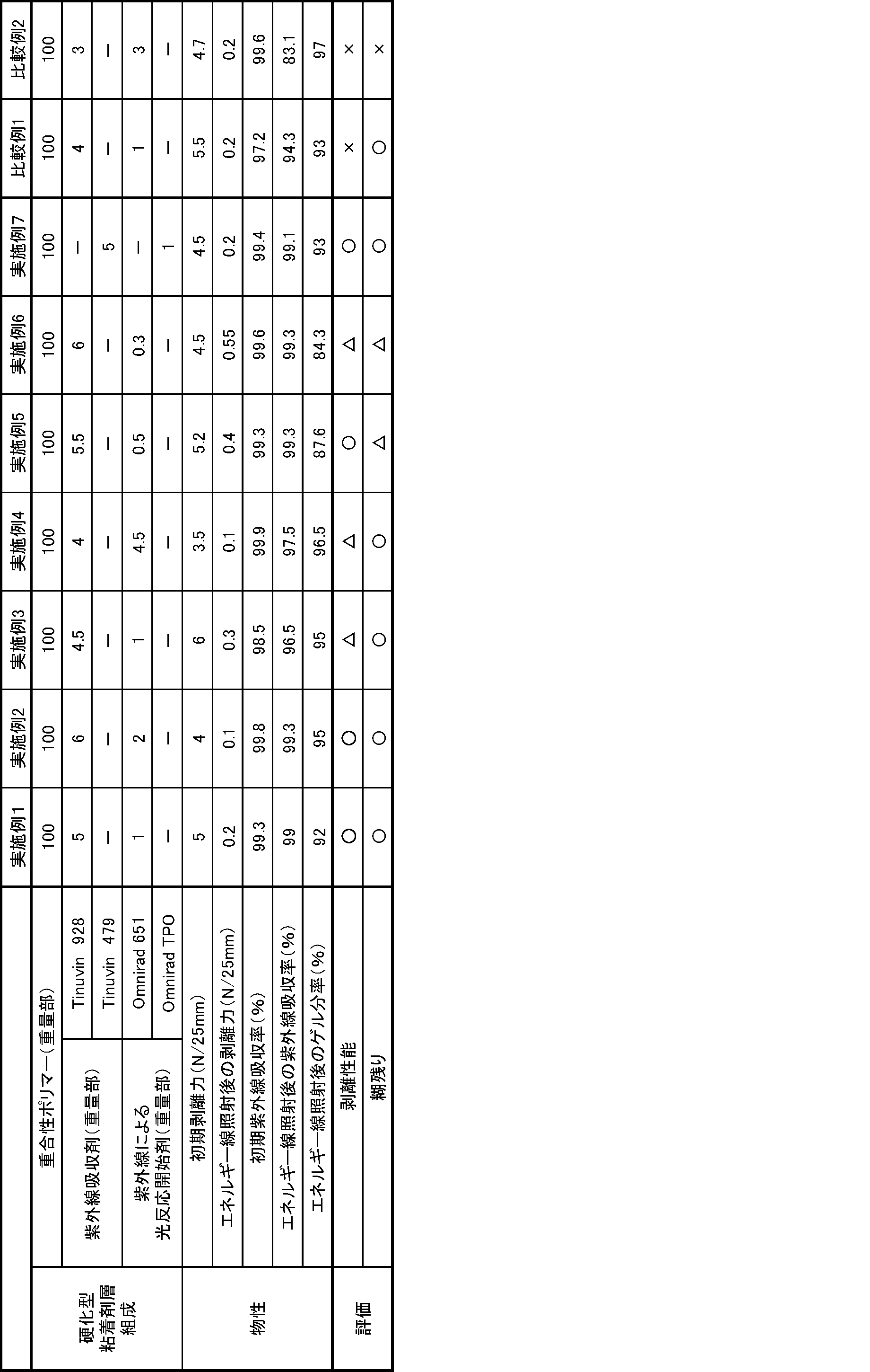
本発明によれば、チップ部品への糊残りを抑制し、かつ、チップ部品を歩留まりよく転写することができる電子部品の製造方法、該電子部品の製造方法を用いた表示装置の製造方法、及び、該製造方法に用いられる支持テープを提供することができる。
1 チップ部品
2 部材
3 支持テープ
4 支持体
5 次部材
6 光照射装置
6a 光
2 部材
3 支持テープ
4 支持体
5 次部材
6 光照射装置
6a 光
Claims (14)
- 少なくとも1つの表面に硬化型粘着剤層を有する支持テープの前記硬化型粘着剤層上にチップ部品を配置する工程(1)と、
前記チップ部品が配置された前記支持テープの前記チップ部品が積層した面とは反対側の面よりエネルギー線を照射する工程(2)と、
前記支持テープの前記チップ部品が積層した面とは反対側の面より刺激を加え、チップ部品を支持テープから次部材へ転写する工程(3)とを有し、
前記硬化型粘着剤層は重合性ポリマーと反応開始剤とを含有し、
前記硬化型粘着剤層は、前記エネルギー線照射前の365nmの波長における紫外線吸収率が95%以上であり、
前記エネルギー線照射後の365nmの波長における紫外線吸収率が95%以上である、
電子部品の製造方法。 - 前記エネルギー線は300nm以上450nm以下の波長の光である、請求項1記載の電子部品の製造方法。
- 前記刺激が300nm以上370nm以下の波長のレーザーである、請求項1又は2記載の電子部品の製造方法。
- 前記硬化型粘着剤層は、紫外線吸収剤を含有する、請求項1~3のいずれかに記載の電子部品の製造方法。
- 前記硬化型粘着剤層は、紫外線による光反応開始剤と紫外線による光反応開始剤以外の紫外線吸収剤とを含有する、請求項4に記載の電子部品の製造方法。
- 前記紫外線吸収剤の合計含有量が前記重合性ポリマー100重量部に対して6重量部以上である、請求項4又は5記載の電子部品の製造方法。
- 前記紫外線による光反応開始剤の含有量は、前記重合性ポリマー100重量部に対して1重量部以上であり、前記紫外線吸収剤の合計100重量%に対して50重量%以下であることを特徴とする請求項5又は6に記載の電子部品の製造方法。
- 前記硬化型粘着剤層の前記エネルギー線照射後の前記紫外線吸収率が99%以上である、請求項1~7のいずれかに記載の電子部品の製造方法。
- 前記硬化型粘着剤層の前記エネルギー線照射後のゲル分率が90%以上である、請求項1~8のいずれかに記載の電子部品の製造方法。
- 前記エネルギー線照射後における前記硬化型粘着剤層の剥離力が0.5N/25mm以下である、請求項1~9のいずれかに記載の電子部品の製造方法。
- 前記支持テープは、両面粘着テープであり、前記両面粘着テープは、前記チップ部品が配置されない面の粘着剤層の300~450nmのエネルギー線透過率が90%以上である、請求項1~10のいずれかに記載の電子部品の製造方法。
- 前記支持テープは、基材を有し、前記基材の300~450nmのエネルギー線透過率が90%以上である、請求項1~11のいずれかに記載の電子部品の製造方法。
- 少なくとも1つの表面に硬化型粘着剤層を有する支持テープの前記硬化型粘着剤層上にマイクロLEDチップを配置する工程(1)と、
前記マイクロLEDチップが配置された前記支持テープの前記マイクロLEDチップが積層した面とは反対側の面よりエネルギー線を照射する工程(2)と、
前記支持テープの前記マイクロLEDチップが積層した面とは反対側の面より刺激を加え、マイクロLEDチップを支持テープから次部材へ転写する工程(3)とを有し、
前記硬化型粘着剤層は、重合性ポリマーと反応開始剤とを含有し、
前記硬化型粘着剤層は、前記エネルギー線照射前の365nmの波長における紫外線吸収率が99%以上であり、
前記エネルギー線照射後の365nmの波長における紫外線吸収率が95%以上である、
表示装置の製造方法。 - 少なくとも1つの表面に硬化型粘着剤層を有する支持テープであり、
前記硬化型粘着剤層は重合性ポリマーと反応開始剤とを含有し、
前記硬化型粘着剤層は、エネルギー線照射前の365nmの波長における紫外線吸収率が95%以上であり、
前記エネルギー線照射後の365nmの波長における紫外線吸収率が95%以上である、支持テープ。
Priority Applications (3)
| Application Number | Priority Date | Filing Date | Title |
|---|---|---|---|
| CN202180068048.4A CN116438274A (zh) | 2020-11-13 | 2021-11-11 | 电子部件的制造方法、显示装置的制造方法及支撑带 |
| EP21891936.3A EP4227378A4 (en) | 2020-11-13 | 2021-11-11 | METHOD FOR PRODUCING ELECTRONIC COMPONENT, METHOD FOR PRODUCING DISPLAY DEVICE, AND SUPPORT TAPE |
| JP2022517220A JP7256333B2 (ja) | 2020-11-13 | 2021-11-11 | 電子部品の製造方法、表示装置の製造方法、及び、支持テープ |
Applications Claiming Priority (2)
| Application Number | Priority Date | Filing Date | Title |
|---|---|---|---|
| JP2020-189556 | 2020-11-13 | ||
| JP2020189556 | 2020-11-13 |
Publications (1)
| Publication Number | Publication Date |
|---|---|
| WO2022102691A1 true WO2022102691A1 (ja) | 2022-05-19 |
Family
ID=81601296
Family Applications (1)
| Application Number | Title | Priority Date | Filing Date |
|---|---|---|---|
| PCT/JP2021/041471 Ceased WO2022102691A1 (ja) | 2020-11-13 | 2021-11-11 | 電子部品の製造方法、表示装置の製造方法、及び、支持テープ |
Country Status (4)
| Country | Link |
|---|---|
| EP (1) | EP4227378A4 (ja) |
| JP (2) | JP7256333B2 (ja) |
| CN (1) | CN116438274A (ja) |
| WO (1) | WO2022102691A1 (ja) |
Cited By (3)
| Publication number | Priority date | Publication date | Assignee | Title |
|---|---|---|---|---|
| WO2022244756A1 (ja) * | 2021-05-17 | 2022-11-24 | 積水化学工業株式会社 | 粘着テープ |
| WO2023243475A1 (ja) * | 2022-06-17 | 2023-12-21 | 日産化学株式会社 | 光照射剥離用の接着剤組成物、積層体、及び加工された半導体基板又は電子デバイス層の製造方法 |
| WO2024062974A1 (ja) * | 2022-09-22 | 2024-03-28 | 日産化学株式会社 | 光照射剥離用の剥離剤組成物、積層体、及び加工された半導体基板の製造方法 |
Families Citing this family (1)
| Publication number | Priority date | Publication date | Assignee | Title |
|---|---|---|---|---|
| JP2023008789A (ja) * | 2021-07-02 | 2023-01-19 | 日鉄ケミカル&マテリアル株式会社 | 接着剤層形成用組成物、積層体、積層体の製造方法および積層体の処理方法 |
Citations (6)
| Publication number | Priority date | Publication date | Assignee | Title |
|---|---|---|---|---|
| JP2003007986A (ja) | 2001-06-27 | 2003-01-10 | Sony Corp | 素子の転写方法及びこれを用いた素子の配列方法、画像表示装置の製造方法 |
| JP2005005494A (ja) * | 2003-06-12 | 2005-01-06 | Sony Corp | チップ部品の実装方法及び実装基板 |
| JP2017135397A (ja) * | 2011-03-30 | 2017-08-03 | ボンドテック株式会社 | 電子部品実装方法および電子部品実装システム |
| US20180374738A1 (en) * | 2017-06-23 | 2018-12-27 | Samsung Electronics Co., Ltd. | Chip mounting apparatus and method using the same |
| JP2019015899A (ja) | 2017-07-10 | 2019-01-31 | 株式会社ブイ・テクノロジー | 表示装置の製造方法、チップ部品の転写方法、および転写部材 |
| JP2019138949A (ja) | 2018-02-06 | 2019-08-22 | 株式会社ブイ・テクノロジー | Ledディスプレイの製造方法 |
Family Cites Families (5)
| Publication number | Priority date | Publication date | Assignee | Title |
|---|---|---|---|---|
| JP2007238802A (ja) | 2006-03-09 | 2007-09-20 | Sekisui Chem Co Ltd | 電子部品の加工方法 |
| US20140103499A1 (en) * | 2012-10-11 | 2014-04-17 | International Business Machines Corporation | Advanced handler wafer bonding and debonding |
| JP2015056446A (ja) | 2013-09-10 | 2015-03-23 | 古河電気工業株式会社 | 半導体ウエハ表面保護用粘着テープおよび半導体ウエハの加工方法 |
| JP6446205B2 (ja) | 2014-08-29 | 2018-12-26 | 大倉工業株式会社 | 床面養生用シート |
| US9418895B1 (en) * | 2015-03-14 | 2016-08-16 | International Business Machines Corporation | Dies for RFID devices and sensor applications |
-
2021
- 2021-11-11 CN CN202180068048.4A patent/CN116438274A/zh active Pending
- 2021-11-11 WO PCT/JP2021/041471 patent/WO2022102691A1/ja not_active Ceased
- 2021-11-11 JP JP2022517220A patent/JP7256333B2/ja active Active
- 2021-11-11 EP EP21891936.3A patent/EP4227378A4/en active Pending
-
2023
- 2023-03-30 JP JP2023054492A patent/JP2023098907A/ja active Pending
Patent Citations (6)
| Publication number | Priority date | Publication date | Assignee | Title |
|---|---|---|---|---|
| JP2003007986A (ja) | 2001-06-27 | 2003-01-10 | Sony Corp | 素子の転写方法及びこれを用いた素子の配列方法、画像表示装置の製造方法 |
| JP2005005494A (ja) * | 2003-06-12 | 2005-01-06 | Sony Corp | チップ部品の実装方法及び実装基板 |
| JP2017135397A (ja) * | 2011-03-30 | 2017-08-03 | ボンドテック株式会社 | 電子部品実装方法および電子部品実装システム |
| US20180374738A1 (en) * | 2017-06-23 | 2018-12-27 | Samsung Electronics Co., Ltd. | Chip mounting apparatus and method using the same |
| JP2019015899A (ja) | 2017-07-10 | 2019-01-31 | 株式会社ブイ・テクノロジー | 表示装置の製造方法、チップ部品の転写方法、および転写部材 |
| JP2019138949A (ja) | 2018-02-06 | 2019-08-22 | 株式会社ブイ・テクノロジー | Ledディスプレイの製造方法 |
Non-Patent Citations (1)
| Title |
|---|
| See also references of EP4227378A4 |
Cited By (3)
| Publication number | Priority date | Publication date | Assignee | Title |
|---|---|---|---|---|
| WO2022244756A1 (ja) * | 2021-05-17 | 2022-11-24 | 積水化学工業株式会社 | 粘着テープ |
| WO2023243475A1 (ja) * | 2022-06-17 | 2023-12-21 | 日産化学株式会社 | 光照射剥離用の接着剤組成物、積層体、及び加工された半導体基板又は電子デバイス層の製造方法 |
| WO2024062974A1 (ja) * | 2022-09-22 | 2024-03-28 | 日産化学株式会社 | 光照射剥離用の剥離剤組成物、積層体、及び加工された半導体基板の製造方法 |
Also Published As
| Publication number | Publication date |
|---|---|
| EP4227378A1 (en) | 2023-08-16 |
| CN116438274A (zh) | 2023-07-14 |
| JP2023098907A (ja) | 2023-07-11 |
| TW202235576A (zh) | 2022-09-16 |
| JPWO2022102691A1 (ja) | 2022-05-19 |
| JP7256333B2 (ja) | 2023-04-11 |
| EP4227378A4 (en) | 2025-02-12 |
Similar Documents
| Publication | Publication Date | Title |
|---|---|---|
| JP7256333B2 (ja) | 電子部品の製造方法、表示装置の製造方法、及び、支持テープ | |
| JP7510300B2 (ja) | 粘着テープ | |
| KR101516147B1 (ko) | 웨이퍼의 처리 방법 | |
| JP7594436B2 (ja) | 粘着テープ | |
| JP2019031620A (ja) | 再剥離性粘着剤組成物 | |
| JP2018147988A (ja) | 半導体チップの製造方法 | |
| JP2024163338A (ja) | 粘着テープ | |
| JP5555578B2 (ja) | 粘着剤組成物及び粘着テープ | |
| JP6266993B2 (ja) | ウエハの処理方法 | |
| KR102939975B1 (ko) | 전자 부품의 제조 방법, 및, 표시 장치의 제조 방법 | |
| JP6713864B2 (ja) | 半導体チップの製造方法及びウエハ仮固定用粘着テープ | |
| TWI918765B (zh) | 電子零件之製造方法、顯示裝置之製造方法、及支持帶 | |
| JP2019070094A (ja) | 両面粘着テープ及び半導体装置の製造方法 | |
| JP2024144717A (ja) | 粘着テープ | |
| JP5328132B2 (ja) | 半導体加工用テープ | |
| JP6568373B2 (ja) | 接着剤組成物、及び、接着テープ | |
| JP7672969B2 (ja) | 半導体装置の製造方法、及び、半導体加工用積層体 | |
| TWI889721B (zh) | 半導體加工用積層體、半導體加工用黏著帶、及半導體裝置之製造方法 | |
| JP6564325B2 (ja) | ウエハの処理方法 | |
| JP7100957B2 (ja) | 半導体保護テープ | |
| JP2020186313A (ja) | 半導体加工用粘着テープ | |
| JP2017082094A (ja) | 半導体加工用両面粘着テープ | |
| JP2025104842A (ja) | 粘着テープ | |
| JP6285738B2 (ja) | ウエハの処理方法 | |
| JP2024061681A (ja) | 半導体製造工程用粘着テープ |
Legal Events
| Date | Code | Title | Description |
|---|---|---|---|
| ENP | Entry into the national phase |
Ref document number: 2022517220 Country of ref document: JP Kind code of ref document: A |
|
| 121 | Ep: the epo has been informed by wipo that ep was designated in this application |
Ref document number: 21891936 Country of ref document: EP Kind code of ref document: A1 |
|
| ENP | Entry into the national phase |
Ref document number: 2021891936 Country of ref document: EP Effective date: 20230512 |
|
| NENP | Non-entry into the national phase |
Ref country code: DE |