WO2022103200A1 - 발광 모듈, 이를 제조하는 방법 및 이를 포함하는 디스플레이 장치 - Google Patents
발광 모듈, 이를 제조하는 방법 및 이를 포함하는 디스플레이 장치 Download PDFInfo
- Publication number
- WO2022103200A1 WO2022103200A1 PCT/KR2021/016539 KR2021016539W WO2022103200A1 WO 2022103200 A1 WO2022103200 A1 WO 2022103200A1 KR 2021016539 W KR2021016539 W KR 2021016539W WO 2022103200 A1 WO2022103200 A1 WO 2022103200A1
- Authority
- WO
- WIPO (PCT)
- Prior art keywords
- molding
- layer
- molding layer
- circuit board
- light emitting
- Prior art date
- Legal status (The legal status is an assumption and is not a legal conclusion. Google has not performed a legal analysis and makes no representation as to the accuracy of the status listed.)
- Ceased
Links
Images




Classifications
-
- H—ELECTRICITY
- H10—SEMICONDUCTOR DEVICES; ELECTRIC SOLID-STATE DEVICES NOT OTHERWISE PROVIDED FOR
- H10H—INORGANIC LIGHT-EMITTING SEMICONDUCTOR DEVICES HAVING POTENTIAL BARRIERS
- H10H20/00—Individual inorganic light-emitting semiconductor devices having potential barriers, e.g. light-emitting diodes [LED]
- H10H20/80—Constructional details
- H10H20/85—Packages
- H10H20/8506—Containers
-
- H—ELECTRICITY
- H10—SEMICONDUCTOR DEVICES; ELECTRIC SOLID-STATE DEVICES NOT OTHERWISE PROVIDED FOR
- H10H—INORGANIC LIGHT-EMITTING SEMICONDUCTOR DEVICES HAVING POTENTIAL BARRIERS
- H10H29/00—Integrated devices, or assemblies of multiple devices, comprising at least one light-emitting semiconductor element covered by group H10H20/00
- H10H29/80—Constructional details
- H10H29/842—Coatings, e.g. passivation layers or antireflective coatings
-
- H—ELECTRICITY
- H10—SEMICONDUCTOR DEVICES; ELECTRIC SOLID-STATE DEVICES NOT OTHERWISE PROVIDED FOR
- H10H—INORGANIC LIGHT-EMITTING SEMICONDUCTOR DEVICES HAVING POTENTIAL BARRIERS
- H10H20/00—Individual inorganic light-emitting semiconductor devices having potential barriers, e.g. light-emitting diodes [LED]
- H10H20/01—Manufacture or treatment
- H10H20/036—Manufacture or treatment of packages
- H10H20/0362—Manufacture or treatment of packages of encapsulations
-
- H—ELECTRICITY
- H10—SEMICONDUCTOR DEVICES; ELECTRIC SOLID-STATE DEVICES NOT OTHERWISE PROVIDED FOR
- H10H—INORGANIC LIGHT-EMITTING SEMICONDUCTOR DEVICES HAVING POTENTIAL BARRIERS
- H10H20/00—Individual inorganic light-emitting semiconductor devices having potential barriers, e.g. light-emitting diodes [LED]
- H10H20/01—Manufacture or treatment
- H10H20/036—Manufacture or treatment of packages
- H10H20/0363—Manufacture or treatment of packages of optical field-shaping means
-
- H—ELECTRICITY
- H10—SEMICONDUCTOR DEVICES; ELECTRIC SOLID-STATE DEVICES NOT OTHERWISE PROVIDED FOR
- H10H—INORGANIC LIGHT-EMITTING SEMICONDUCTOR DEVICES HAVING POTENTIAL BARRIERS
- H10H20/00—Individual inorganic light-emitting semiconductor devices having potential barriers, e.g. light-emitting diodes [LED]
- H10H20/80—Constructional details
- H10H20/85—Packages
- H10H20/852—Encapsulations
- H10H20/853—Encapsulations characterised by their shape
-
- H—ELECTRICITY
- H10—SEMICONDUCTOR DEVICES; ELECTRIC SOLID-STATE DEVICES NOT OTHERWISE PROVIDED FOR
- H10H—INORGANIC LIGHT-EMITTING SEMICONDUCTOR DEVICES HAVING POTENTIAL BARRIERS
- H10H20/00—Individual inorganic light-emitting semiconductor devices having potential barriers, e.g. light-emitting diodes [LED]
- H10H20/80—Constructional details
- H10H20/85—Packages
- H10H20/852—Encapsulations
- H10H20/854—Encapsulations characterised by their material, e.g. epoxy or silicone resins
-
- H—ELECTRICITY
- H10—SEMICONDUCTOR DEVICES; ELECTRIC SOLID-STATE DEVICES NOT OTHERWISE PROVIDED FOR
- H10H—INORGANIC LIGHT-EMITTING SEMICONDUCTOR DEVICES HAVING POTENTIAL BARRIERS
- H10H20/00—Individual inorganic light-emitting semiconductor devices having potential barriers, e.g. light-emitting diodes [LED]
- H10H20/80—Constructional details
- H10H20/85—Packages
- H10H20/855—Optical field-shaping means, e.g. lenses
-
- H—ELECTRICITY
- H10—SEMICONDUCTOR DEVICES; ELECTRIC SOLID-STATE DEVICES NOT OTHERWISE PROVIDED FOR
- H10H—INORGANIC LIGHT-EMITTING SEMICONDUCTOR DEVICES HAVING POTENTIAL BARRIERS
- H10H29/00—Integrated devices, or assemblies of multiple devices, comprising at least one light-emitting semiconductor element covered by group H10H20/00
- H10H29/80—Constructional details
- H10H29/85—Packages
- H10H29/852—Encapsulations
-
- H—ELECTRICITY
- H10—SEMICONDUCTOR DEVICES; ELECTRIC SOLID-STATE DEVICES NOT OTHERWISE PROVIDED FOR
- H10H—INORGANIC LIGHT-EMITTING SEMICONDUCTOR DEVICES HAVING POTENTIAL BARRIERS
- H10H29/00—Integrated devices, or assemblies of multiple devices, comprising at least one light-emitting semiconductor element covered by group H10H20/00
- H10H29/80—Constructional details
- H10H29/882—Scattering means
-
- H—ELECTRICITY
- H10—SEMICONDUCTOR DEVICES; ELECTRIC SOLID-STATE DEVICES NOT OTHERWISE PROVIDED FOR
- H10W—GENERIC PACKAGES, INTERCONNECTIONS, CONNECTORS OR OTHER CONSTRUCTIONAL DETAILS OF DEVICES COVERED BY CLASS H10
- H10W90/00—Package configurations
-
- G—PHYSICS
- G02—OPTICS
- G02B—OPTICAL ELEMENTS, SYSTEMS OR APPARATUS
- G02B1/00—Optical elements characterised by the material of which they are made; Optical coatings for optical elements
- G02B1/10—Optical coatings produced by application to, or surface treatment of, optical elements
- G02B1/11—Anti-reflection coatings
-
- H—ELECTRICITY
- H10—SEMICONDUCTOR DEVICES; ELECTRIC SOLID-STATE DEVICES NOT OTHERWISE PROVIDED FOR
- H10H—INORGANIC LIGHT-EMITTING SEMICONDUCTOR DEVICES HAVING POTENTIAL BARRIERS
- H10H29/00—Integrated devices, or assemblies of multiple devices, comprising at least one light-emitting semiconductor element covered by group H10H20/00
- H10H29/80—Constructional details
- H10H29/85—Packages
- H10H29/852—Encapsulations
- H10H29/853—Encapsulations characterised by their shape
-
- H—ELECTRICITY
- H10—SEMICONDUCTOR DEVICES; ELECTRIC SOLID-STATE DEVICES NOT OTHERWISE PROVIDED FOR
- H10H—INORGANIC LIGHT-EMITTING SEMICONDUCTOR DEVICES HAVING POTENTIAL BARRIERS
- H10H29/00—Integrated devices, or assemblies of multiple devices, comprising at least one light-emitting semiconductor element covered by group H10H20/00
- H10H29/80—Constructional details
- H10H29/85—Packages
- H10H29/852—Encapsulations
- H10H29/854—Encapsulations characterised by their material, e.g. epoxy or silicone resins
-
- H—ELECTRICITY
- H10—SEMICONDUCTOR DEVICES; ELECTRIC SOLID-STATE DEVICES NOT OTHERWISE PROVIDED FOR
- H10H—INORGANIC LIGHT-EMITTING SEMICONDUCTOR DEVICES HAVING POTENTIAL BARRIERS
- H10H29/00—Integrated devices, or assemblies of multiple devices, comprising at least one light-emitting semiconductor element covered by group H10H20/00
- H10H29/80—Constructional details
- H10H29/85—Packages
- H10H29/855—Optical field-shaping means, e.g. lenses
- H10H29/8552—Light absorbing arrangements, e.g. black matrix
Definitions
- the present invention relates to a light emitting module, a method of manufacturing the same, and a display device including the same, and more particularly, to a light emitting module including a molding unit surrounding a plurality of unit pixels.
- a light emitting device is a semiconductor device using a light emitting diode, which is an inorganic light source, and is used in various fields such as display devices, vehicle lamps, and general lighting.
- Light emitting diodes have long lifespan, low power consumption, and fast response speed, so they are rapidly replacing existing light sources.
- a conventional light emitting diode has been mainly used as a backlight light source in a display device.
- a display device that directly implements an image using a light emitting diode has been developed. Such displays are also referred to as microLED displays.
- a display device generally implements various colors by using a mixture of blue, green, and red colors.
- a display device includes a plurality of pixels to implement various images, and each pixel includes blue, green, and red sub-pixels. A color of a specific pixel is determined through the color of these sub-pixels, and an image is implemented by a combination of these pixels.
- microLEDs are arranged on a plane corresponding to each sub-pixel, and a large number of microLEDs are mounted on one substrate.
- microLEDs are very small at 200 ⁇ m or less and even less than 100 ⁇ m, so it is difficult to transfer them to a circuit board.
- An object of the present invention is to provide a light emitting module having an improved structure and a method of manufacturing the same to alleviate a color difference that may be caused by a circuit board and minimize luminance loss.
- Another problem to be solved by the present invention is to provide a light emitting module capable of enhancing durability and a method of manufacturing the same.
- a light emitting module includes a circuit board, a plurality of unit pixels arranged on the circuit board, and a molding unit covering the plurality of unit pixels.
- the molding part includes a first molding layer that at least partially covers each of the unit pixels, and a second molding layer that covers the first molding layer.
- the light emitting module may include an anti-glare layer disposed on the molding part.
- the first molding layer may include a black molding layer
- the second molding layer may include a transparent molding layer
- the first molding layer may include a transparent molding layer
- the second molding layer may include a black molding layer
- the first molding layer may cover a side surface and an upper surface of each of the unit pixels, and the second molding layer may be disposed on the first molding layer.
- the first molding layer may at least partially cover a side surface of the unit pixel, and the second molding layer may cover the first molding layer. Furthermore, the first molding layer may have a concave shape in a region between the unit pixels.
- a portion of the second molding layer may be located in an area between unit pixels.
- the first molding layer may cover upper surfaces of the unit pixels, and the first molding layer positioned on the unit pixels may have a convex shape.
- a top profile of the second molding layer may be substantially flat regardless of a profile of the circuit board. In another embodiment, a top surface profile of the second molding layer may be substantially the same as a profile of the circuit board.
- a top surface of the circuit board may be non-planar, and the first and second molding layers may each have a flat top surface.
- the light emitting module may further include an anti-reflection layer disposed between the molding part and the anti-glare layer.
- the light emitting module may further include a hardness-reinforcing layer disposed between the molding part and the anti-glare layer.
- a method of manufacturing a light emitting module includes mounting a plurality of unit pixels on a circuit board, and forming a molding part covering the plurality of unit pixels on the circuit board.
- the molding part includes a first molding layer that at least partially covers each of the unit pixels, and a second molding layer that covers the first molding layer. Furthermore, an anti-glare layer may be formed on the molding part.
- the method of manufacturing the light emitting module may further include cutting edges of the anti-glare layer, the molding part, and the circuit board.
- forming the molding part includes applying a first molding solution and provisionally curing to form a first molding layer that is temporarily cured, and placing a plate on the first molding layer that is temporarily cured to provide the temporary curing.
- Forming a molding layer, placing a plate on the pre-cured second molding layer, applying pressure to the pre-cured second molding layer, and curing the first molding layer and the second molding layer with ultraviolet rays may include
- the first molding liquid may be applied to have a first portion applied to a central portion of the circuit board, and second portions extending from the first portion to corners of the circuit board.
- the second molding liquid may be applied to have a first portion applied to a central portion of the circuit board, and second portions extending from the first portion to corners of the circuit board.
- Ends of the second portions may be spaced apart from corners of the circuit board, respectively.
- a first molding layer is formed by spraying a first molding liquid on the circuit board using an inkjet technique, and a second molding liquid is applied on the first molding layer. It may include spraying to form a second molding layer.
- the first molding layer may be formed of a black molding layer, and the second molding layer may be formed of a transparent molding layer.
- the first molding layer may be formed of a transparent molding layer, and the second molding layer may be formed of a black molding layer.
- the method of manufacturing the light emitting module may further include forming an anti-reflection layer on the molding part before forming the anti-glare layer.
- the method of manufacturing the light emitting module may further include forming a hardness-reinforcing layer before forming the anti-glare layer.
- a display device includes a panel substrate and a plurality of light emitting modules arranged on the panel substrate.
- Each of the light emitting modules includes a circuit board, a plurality of unit pixels arranged on the circuit board, and a molding unit covering the plurality of unit pixels.
- the molding unit may include a first molding layer that at least partially covers each of the unit pixels, and a second molding layer that covers the first molding layer.
- each of the light emitting modules may include an anti-glare layer disposed on the molding part.
- a light emitting module that improves color difference and minimizes luminance loss by arranging a molding part including a black molding layer and a transparent molding layer on a circuit board to surround a plurality of unit pixels. there is.
- a light emitting module having improved surface hardness by disposing a hardness-reinforced layer on a molding unit surrounding a plurality of unit pixels may be provided.
- FIG. 1A is a schematic plan view illustrating a display device according to an exemplary embodiment.
- Fig. 1B is a schematic cross-sectional view taken along line A-A' of Fig. 1A;
- 2A is a schematic plan view for explaining a light emitting module according to an embodiment.
- Fig. 2B is a schematic cross-sectional view taken along line B-B' of Fig. 2A;
- 3A is a schematic cross-sectional view for explaining a light emitting module according to another embodiment of the present disclosure.
- 3B is a schematic cross-sectional view for explaining a light emitting module according to another embodiment of the present disclosure.
- FIG. 4 is a schematic cross-sectional view for explaining a light emitting module according to another embodiment of the present disclosure.
- FIG. 5 is a schematic cross-sectional view for explaining a light emitting module according to another embodiment of the present disclosure.
- FIG. 6 is a schematic cross-sectional view for explaining a light emitting module according to another embodiment of the present disclosure.
- FIGS. 7A to 7G are schematic cross-sectional views for explaining a method of manufacturing a light emitting module according to an embodiment.
- FIG. 8 is a schematic plan view for explaining a method of manufacturing a light emitting module according to an embodiment.
- 9A to 9H are schematic cross-sectional views for explaining a method of manufacturing a light emitting module according to another embodiment of the present disclosure.
- 10A to 10H are schematic cross-sectional views for explaining a method of manufacturing a light emitting module according to another embodiment of the present disclosure.
- FIG. 11 is a schematic cross-sectional view illustrating a side shape of a molding part that may be generated in a light emitting module manufacturing process.
- 12A to 12E are schematic cross-sectional views for explaining a method of manufacturing a light emitting module according to another embodiment of the present disclosure.
- 13A, 13B, and 13C are schematic cross-sectional views for explaining various unit pixels of the present disclosure.
- FIG. 1A is a schematic plan view for explaining a display device according to an exemplary embodiment
- FIG. 1B is a schematic cross-sectional view taken along line A-A' of FIG. 1A.
- the display apparatus 1000 may include a panel substrate 200 and a plurality of light emitting modules 100 .
- Each light emitting module 100 may include a plurality of unit pixels 10 .
- the display device 1000 is not particularly limited, but may include a VR display device such as a micro LED TV, a smart watch, a VR headset, or an AR display device such as augmented reality glasses.
- a VR display device such as a micro LED TV, a smart watch, a VR headset, or an AR display device such as augmented reality glasses.
- the panel substrate 200 may be formed of a material such as PI (Polyimide), FR4, or glass, and may include a circuit for passive matrix driving or active matrix driving.
- the panel substrate 200 may include a wiring and a resistor therein.
- the panel substrate 200 may include wirings, transistors, and capacitors.
- the panel substrate 200 may have pads electrically connected to a circuit on its upper surface.
- a plurality of light emitting modules 100 may be arranged on the panel substrate 200 .
- the light emitting modules 100 may be disposed to be spaced apart from each other or disposed to be in close contact with each other.
- the interval between the light emitting modules 100 may be set in consideration of the interval between the unit pixels 10 to be described later.
- the spacing between two adjacent unit pixels 10 respectively disposed in the adjacent light emitting modules 100 may be substantially the same as the spacing between the unit pixels 10 in one light emitting module 100 .
- the light emitting module 100 will be described in detail with reference to FIGS. 2A and 2B .
- FIG. 2A is a plan view illustrating one light emitting module 100 according to an embodiment of the present invention
- FIG. 2B is a schematic cross-sectional view taken along line B-B' of FIG. 2A.
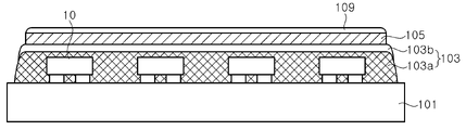
- the light emitting module 100 includes a circuit board 101 , a plurality of unit pixels 10 , a molding part 103 , and an anti-glare layer 109 .
- the molding part 103 may include a first molding layer 103a and a second molding layer 103b.
- the circuit board 101 may include a circuit for electrically connecting the panel board 200 and the plurality of unit pixels 10 .
- the circuit in the circuit board 101 may be formed in a multi-layered structure.
- the circuit board 101 may include a passive circuit for driving the plurality of unit pixels 10 by a passive matrix driving method or an active circuit for driving the plurality of unit pixels 10 by an active matrix driving method.
- the circuit board 101 may have exposed pads on the surface, and the plurality of unit pixels 10 may be bonded to the pads of the circuit board 101 through a bonding material.
- the circuit board 101 may be a black circuit board 101 suitable for a display device.
- the plurality of unit pixels 10 are arranged on the circuit board 101 .
- the plurality of unit pixels 10 may include a plurality of light emitting devices emitting red light, green light, and blue light, respectively. Each of the light emitting elements may correspond to a sub-pixel.
- the unit pixel 10 may include at least three light emitting devices arranged on the same plane.
- the unit pixel 10a may include at least three light emitting devices 13a , 13b , and 13c disposed to be spaced apart from each other on a transparent substrate 11 , the transparent substrate Light emitting devices 13a , 13b , and 13c together with the transparent substrate 11 may be disposed on the circuit board 101 to emit light through ( 11 ).
- the plurality of unit pixels 10b may include at least three light emitting devices 13a , 13b , and 13c spaced apart from each other.
- the unit pixel 10c may include the light emitting devices 13a , 13b , and 13c arranged on the circuit board 101 without the transparent substrate 11 described above. That is, at least three light emitting devices 13a , 13b , and 13c disposed adjacent to each other on the circuit board 101 may constitute one unit pixel 10 .
- the plurality of unit pixels 10c may include a first LED stacked layer 23a, a second LED stacked layer 23b, and a third LED stacked layer 23c stacked in a vertical direction, respectively.
- the first LED stacked layer 23a, the second LED stacked layer 23b, and the third LED stacked layer 23c may each constitute a sub-pixel.
- the unit pixel 10c may include first, second, and third LED stacks 23a, 23b, and 23c vertically stacked on a transparent substrate 21 .
- the first, second, and third LED stacks 23a , 23b , and 23c may be disposed on the circuit board 101 together with the transparent substrate 21 to emit light through the transparent substrate 21 . there is.
- the plurality of unit pixels 10 may be arranged in a matrix form on the circuit board 101 .
- the molding part 103 may include a plurality of molding layers 103a and 103b, and the number of the plurality of molding layers 103a and 103b is not limited.
- the plurality of molding layers 103a and 103b may have different colors and may be made of at least two types of materials.
- the first molding layer 103a may be disposed on the circuit board 101 to cover the plurality of unit pixels 10 . Specifically, the first molding layer 103a may contact the surface of the circuit board 101 and may cover lower surfaces, side surfaces, and upper surfaces of the plurality of unit pixels 10 .
- the first molding layer 103a may have a flat top surface.
- the circuit board 101 may be warped or warped, and thus its surface may not be flat. Even in this case, the first molding layer 103a may have a flat top surface without being affected by the flatness of the circuit board 101 .
- the first molding layer 103a absorbs distortion of the top surface of the circuit board 101 to provide a flat top surface. Accordingly, the first molding layer 103a may include a locally thick portion and a thin portion, and a top surface profile of the first molding layer 103a may be different from a top surface profile of the circuit board 101 .
- the second molding layer 103b may cover a top surface of the first molding layer 103a and may have a flat top surface.
- the second molding layer 103b may have a substantially uniform thickness. Side surfaces of the first molding layer 103a and the second molding layer 103a may be parallel to each other, and these side surfaces may also be parallel to the side surface of the substrate 101 .
- the molding part 103 including the first molding layer 103a and the second molding layer 103b may be formed using an ultraviolet curing resin.
- the ultraviolet curable resin By using the ultraviolet curable resin, the hardness of the molding part 103 may be increased compared to that of the thermosetting resin.
- the present disclosure is not limited thereto, and the molding part 103 may be formed using a thermosetting resin.
- the material of the molding part 103 may include an acryl-based, silicone-based, or urethane-based resin.
- the material of the molding part 103 may further include a light absorber or dye.
- the material of the molding part 103 may be transparent or may be black, white, or gray.
- the first molding layer 103a may be formed of a black molding layer.
- the black molding layer may improve the uniformity of the extracted light by improving the color difference caused by the circuit board 101 .
- the first molding layer 103a surrounds the plurality of unit pixels 10, it is possible to block the light extracted to the side of the unit pixel 10, and accordingly, the left and right viewing angles decrease, and adjacent units It is possible to prevent the boundary lines between pixels from being observed.
- the second molding layer 103b may be formed of a transparent molding layer.
- the transparent molding layer may improve a visual image by eliminating optical distortion of the display apparatus 1000 . Also, by disposing the black molding layer and the transparent molding layer together, in addition to alleviating a color difference caused by the circuit board 101 , luminance may be improved compared to a case in which only the black molding layer is disposed.
- the first molding layer 103a is formed of a black molding layer and that the second molding layer 103b is formed of a transparent molding layer, but the present disclosure is not limited thereto.
- the first molding layer 103a may be formed of a transparent molding layer
- the second molding layer 103b may be formed of a black molding layer.
- the first molding layer 103a may cover upper surfaces of the plurality of unit pixels 10 .
- the thickness of the first molding layer 103a positioned on the upper surface of the unit pixels 10 may be smaller than the width between the unit pixels 10 .
- the anti-glare layer 109 may be disposed on the molding part 103 .
- the anti-glare layer 109 may prevent glare by scattering light by mixing fine particles such as silica, melamine, and acryl with a cured resin.
- the anti-glare layer 109 may maintain high transmittance and improve clarity and smoothness of the surface of the light emitting module 100 .
- the anti-glare layer 109 may include fine particles such as silica, melamine, and acryl, together with polymers such as acryl-based, silicone-based, and urethane-based polymers.
- the anti-glare effect may be controlled by adjusting the thickness of the anti-glare layer 109, the density and size of the particles, and the like.
- each light emitting module 100 includes a molding part 103 . Meanwhile, in addition to the molding part 103 , an additional molding part covering the light emitting modules 100 may be disposed on the panel substrate 200 , and thus, it is possible to prevent the boundary lines of the light emitting modules from being observed. .
- 3A is a schematic cross-sectional view illustrating a light emitting module according to another embodiment of the present disclosure.
- the light emitting module includes a circuit board 101 , a plurality of unit pixels 10 , a first molding layer 103a , a second molding layer 103b , and an anti-glare layer 109 . do.
- the circuit board 101 , the plurality of unit pixels 10 , and the anti-glare layer 109 are similar to those described with reference to FIGS. 2A and 2B , detailed descriptions are omitted to avoid overlapping.
- the first molding layer 103a may be disposed to cover the lower surface and side surfaces of the unit pixels 10 .
- the first molding layer 103a is not disposed on the top surface of the unit pixels 10 , and thus the luminance of the unit pixels may be increased. Meanwhile, the first molding layer 103a may have a concave surface between the unit pixels 10 .
- the first molding layer 103a forms a sidewall in contact with the unit pixel 10 .
- the first molding layer 103a positioned on the side surface of the unit pixel 10 forms a thicker sidewall toward the bottom of the unit pixel 10 . That is, the thickness of the first molding layer 103a in the horizontal direction increases as it approaches the circuit board 101 .
- the second molding layer 103b may be disposed along a concave upper surface of the first molding layer 103a.
- the second molding layer 103b may be formed in a larger amount than that of the first molding layer 103a and may have a flatter upper surface than that of the first molding layer 103a.
- the first molding layer 103a may be formed of a black molding layer, and the second molding layer 103b may be formed of a transparent molding layer. Accordingly, the first molding layer 103a may block light emitted laterally from the lower region of the unit pixel 10 without blocking the light emitted laterally from the upper region of the unit pixel 10 . . Accordingly, the luminance and the beam angle of light emitted from the unit pixels 10 may be increased while effectively preventing the occurrence of optical interference between the unit pixels 10 .
- the present disclosure is not limited thereto, and the first molding layer 103a may be formed of a transparent molding layer, and the second molding layer 103b may be formed of a black molding layer. Accordingly, most of the light emitted to the side of the unit pixels 10 may be blocked.
- the first molding layer 103a and the second molding layer 103b may cover the side and top surfaces of the unit pixel 10 in the same shape regardless of the position of the circuit board 101 .
- the first molding layer 103a and the second molding layer 103b are formed in each of the unit pixels 10 .
- the top profile of the second molding layer 103b may be substantially the same as that of the circuit board 101 .
- 3B is a schematic cross-sectional view for explaining a light emitting module according to another embodiment of the present disclosure.
- the light emitting module according to the present embodiment is substantially similar to the light emitting module described with reference to FIG. 3A , except that the first molding layer 103a covers the upper surfaces of the unit pixels 10 . That is, the first molding layer 103a may cover the upper surface, the side surface, and the lower surface of the unit pixels 10 . However, the first molding layer 103a may have a concave surface in the region between the unit pixels 10 and may have a convex surface on the unit pixels 10 .
- the second molding layer 103b may cover the first molding layer 103a and may have a flat top surface compared to the top surface of the first molding layer 103b.
- the first molding layer 103a and the second molding layer 103b may be formed along the non-planar surface of the circuit board 101 as described with reference to FIG. 3A . Accordingly, substantially the same amount of the first molding layer 103a may be disposed on the unit pixels 10 , and the upper surface of the second molding layer 103b is aligned along the non-planar surface of the circuit board 101 to the circuit board ( 101) may be formed in the same shape as the upper surface.
- FIG. 4 is a schematic cross-sectional view illustrating a light emitting module according to another embodiment of the present disclosure.
- the light emitting module according to the present embodiment includes a circuit board 101 , a plurality of unit pixels 10 , a first molding layer 103a , a second molding layer 103b , and an anti-glare layer. (109) may be included. Since the light emitting module according to the present embodiment is substantially similar to the light emitting module described above with reference to FIGS. 2A and 2B , differences will be described below in order to avoid duplication.
- the first molding layer 103a may be disposed to surround the lower surface and side surfaces of the unit pixels 10 .
- the first molding layer 103a may be formed on the circuit board 101 so that top surfaces of the plurality of unit pixels 10 are exposed.
- the first molding layer 103a may have a flat top surface, and the top surface of the first molding layer 103a may be parallel to the top surface of the unit pixels 10 .
- the second molding layer 103b is disposed on the first molding layer 103a and may be in contact with upper surfaces of the unit pixels 10 .
- the first molding layer 103a may be formed of a black molding layer
- the second molding layer 103b may be formed of a transparent molding layer, but is not limited thereto. This transparent molding layer may be formed, and the second molding layer 103b may be formed of a black molding layer.
- FIG. 5 is a schematic cross-sectional view illustrating a light emitting module according to another embodiment of the present disclosure.
- the light emitting module according to this embodiment is substantially similar to the light emitting module described with reference to FIGS. 2A and 2B , but an anti-reflection layer between the second molding layer 103b and the anti-glare layer 109 . The difference is that it further includes (105).
- the anti-reflection layer 105 prevents light reflection generated on the upper surface of the second molding layer 103b to improve the luminance of the light emitting module.
- the anti-reflection layer 105 may be disposed on the second molding layer 103b using an optical adhesive material.
- the optical adhesive material covers the second molding layer 103b to prevent reflection from the surface of the second molding layer 103b.
- the optical adhesive material may include, for example, acryl-based, silicone-based, and urethane-based components.
- the adhesive may be an amorphous optically clear resin (OCR) in a liquid form, but is not limited thereto, and may be an optically clear adhesive (OCA) in a film form such as a double-sided tape.
- OCR amorphous optically clear resin
- OCA optically clear adhesive
- the anti-reflection layer 105 may be an anti-reflector (AR) coating film in which a polymer material such as polyethylene terephthalate (PET) or tri-acetyl cellulose (TAC) is applied by a wet coating method.
- AR anti-reflector
- the anti-reflection layer 105 may be formed by disposing inorganic material layers having different refractive indices. For example, at least two of the oxide layers such as indium tin oxide (ITO), SiO2, SiON, Si3N4, TiO2, and Ta2O5 are stacked on the second molding layer 103b to form the anti-reflection layer 105.
- the antireflection layer 105 may be formed by attaching a coating film on which oxide layers are laminated on the second molding layer 103b.
- the anti-reflection layer 105 may use the interference of light generated at the interface of the thin films by stacking two or more thin films having different refractive indices. By causing the wavelengths reflected from the interface of each thin film to cause destructive interference with each other, the reflectance of the anti-reflection layer 105 can be reduced and the transmittance can be increased, and thus the luminance of the display device can be increased.
- FIG. 6 is a schematic cross-sectional view illustrating a light emitting module according to another embodiment of the present disclosure.
- the light emitting module according to the present embodiment is substantially similar to the light emitting module described with reference to FIGS. 2A and 2B , but hardness is strengthened between the second molding layer 103b and the anti-glare layer 109 . The difference is that it further includes a layer 107 .
- the hardness-reinforcing layer 107 may be disposed on the second molding layer 103b.
- the hardness-reinforcing layer 107 may be disposed on the second molding layer 103b using an optical adhesive material.
- the hardness-reinforcing layer 107 may include glass or plastic, and the plastic may include, for example, polymethyl methacrylate (PMMA) and polycarbonate.
- the hardness-reinforced layer 107 may have a pencil hardness of 2H or more.
- the light emitting module may further include an anti-reflection layer and an anti-pollution layer.
- the hardness reinforcing layer 107 may be formed of an ultraviolet curing material. In this case, the hardness-reinforced layer 107 may be cured by UV irradiation together with the first and second molding layers 103a and 103b.
- the light emitting module 100 includes a plurality of unit pixels 10 , and the plurality of light emitting modules 100 may be aligned to manufacture the display device 1000 .
- a method of manufacturing the light emitting module will be described in detail.
- FIGS. 7A to 7G are schematic cross-sectional views for explaining a method of manufacturing a light emitting module according to an embodiment of the present invention.
- a plurality of unit pixels 10 are bonded on a circuit board 101 .
- the plurality of unit pixels 10 may be disposed on the upper surface of the circuit board 101 to be spaced apart from each other at regular intervals.
- the electrodes of the unit pixel 10 may be respectively bonded to the electrodes formed on the circuit board 101 through solder, but are not limited thereto, and may be bonded by, for example, eutectic bonding, epoxy bonding, or the like.
- a first molding layer 103a may be formed by coating a molding solution on the circuit board 101 .
- the molding liquid may be applied, coated, or jetted on the circuit board 101, but the present disclosure is not limited thereto. After the molding liquid is applied, the molding liquid may be temporarily cured.
- the first molding layer 103a may be formed by applying a molding solution containing a black pigment. In another embodiment, the first molding layer 103a may be formed by applying a transparent molding solution.
- the present disclosure discloses a method of applying a molding solution and forming the first molding layer 103a to a uniform thickness using the plate 110 .
- the molding liquid When the molding liquid is applied to the entire surface of the circuit board 101 , the molding liquid is accumulated on the edge of the circuit board 101 so that the first molding layer 103a is thickly formed on the edge of the circuit board 101 . .
- the molding liquid may be applied to a portion of the circuit board 101 rather than to the entire surface of the circuit board 101 .
- a larger amount is applied to the central portion compared to other portions of the circuit board 101 so that the central portion may be applied in a convex shape.
- the shape of the molding liquid applied on the circuit board 101 is schematically shown in FIG. 8 . Referring to FIG.
- the molding liquid forming the first molding layer 103a may be applied in a large amount to the central portion of the circuit board 101 , and may be applied in a branch shape from the central portion toward the corners of the circuit board 101 .
- the molding solution may include a first portion applied to the central portion of the circuit board 101 and at least four branch portions directed from the first portion to the corner of the circuit board 101 .
- the amount of the molding liquid applied to the central portion of the circuit board 101 may be greater than the amount of the molding liquid applied to the branch portions.
- the amount of the molding liquid applied to the branch portions may be substantially the same as each other. Meanwhile, the ends of the respective branches are spaced apart from the corners of the circuit board 101 .
- a molding solution may be accumulated on the corners in a subsequent process to increase the thickness of the first molding layer 103a at the corners of the circuit board 101 .
- the second molding layer 103b to be described later may also be formed by applying a molding solution as shown in FIG. 8 in the same manner as the first molding layer 103a.
- a pattern for applying the molding liquid to form the first molding layer 103a and the second molding layer 103b may be various, and is not limited to the present disclosure.
- the molding liquid may be applied in various shapes, such as a "d" pattern, a zigzag pattern, and the like.
- a plate 110 may be disposed on the first molding layer 103a and pressure may be applied to the first molding layer 103a by pressing the plate 110 .
- the plate 110 is not particularly limited, and may be, for example, a glass substrate, a quartz substrate, or an acrylic substrate.
- the shape of the first molding layer 103a may be deformed by the plate 110 .
- the plate 110 may descend to a predetermined height, and the first molding layer 103a may be deformed to a predetermined thickness.
- the first molding layer 103a disposed in the central portion spreads to the peripheral area of the circuit board 101 .
- the lower surface of the plate 110 may be flat, and accordingly, the upper surface of the first molding layer 103a may be deformed to be flat like the lower surface of the plate 110 .
- the top surface of the first molding layer 103a may have a flat surface regardless of the top surface profile of the circuit board 101 .
- the plate 110 may have a nano-pattern or micro-pattern irregularities on its lower surface, and the first molding layer 103a may be deformed to have irregularities along the lower surface shape of the plate 110 .
- a second molding layer 103b may be formed by applying a molding liquid on the first molding layer 103a.
- the molding liquid may be applied, coated, or jetted on the first molding layer 103a having a flat top surface, but is not limited thereto. After the molding liquid is applied, the molding liquid may be temporarily cured.
- the second molding layer 103b may be formed of a transparent molding liquid.
- the first molding layer 103a is a transparent molding layer
- the second molding layer 103b may be formed of a black molding liquid.
- the second molding layer 103b may be formed by applying a molding solution on the first molding layer 103a as in the case of forming the first molding layer 103a above.
- a plate 110 may be disposed on the second molding layer 103b and pressure may be applied to the second molding layer 103b by pressing the plate 110 .
- the plate 110 is not particularly limited, and may be, for example, a glass substrate, a quartz substrate, or an acrylic substrate.
- the plate 110 may be the same as the plate 110 used to form the first molding layer 103a, but is not limited thereto.
- the upper surface of the second molding layer 103b may be deformed by the plate 110 .
- the plate 110 may descend to a predetermined height, and the second molding layer 103b may be deformed to a predetermined thickness.
- a lower surface of the plate 110 may be flat, and an upper surface of the second molding layer 103b may be deformed to be flat.
- the plate 110 may have a nano-pattern or micro-pattern on its lower surface, and the upper surface of the second molding layer 103b may be deformed to have irregularities by the plate 110 pattern. .
- the first molding layer 103a and the second molding layer 103b may be simultaneously cured by irradiating ultraviolet rays, and thus the cured molding part 103 may be formed.
- Ultraviolet rays may be irradiated through the plate 110 .
- the plate 110 may be removed and the anti-glare layer 109 may be formed on the exposed surface of the molding part 103 .
- the anti-glare layer 109 may be coated on the molding part 103 using a spray coating technique.
- the anti-glare layer 109 may be cured using ultraviolet rays.
- the light emitting module may be completed by cutting and removing the edge of the circuit board 101 .
- the circuit board 101 , the molding part 103 , and the anti-glare layer 109 may be cut together using a technique such as dicing, laser cutting, or routing.
- the circuit board 101 , the molding part 103 , and the anti-glare layer 109 may have side surfaces parallel to each other by cutting.
- Degree. 9A to 9H are schematic cross-sectional views for explaining a method of manufacturing a light emitting module according to another embodiment of the present invention.
- a description overlapping with the description of the light emitting module manufacturing method of FIGS. 7A to 7G will be omitted.
- a plurality of unit pixels 10 are bonded on a circuit board 101 . A description thereof will be omitted since it is the same as that described with reference to FIG. 7A.
- a first molding layer 103a covering a plurality of unit pixels 10 is formed on the circuit board 101 , and a second molding layer 103b is formed on the first molding layer 103b .
- a layer 103b may be formed.
- an anti-reflection layer 105 may be formed on the second molding layer 103b.
- An optically clear resin (OCR) may be disposed between the second molding layer 103b and the antireflection layer 105 for adhesion of the antireflection layer 105 .
- the anti-reflection layer 105 may be in the form of an anti-reflector (AR) coating film.
- the anti-reflection layer 105 may be formed on the second molding layer 103b through a deposition process.
- an anti-glare layer 109 may be disposed on the anti-reflective layer 105 to prevent glare by scattering light.
- the description of the anti-glare layer 109 is the same as that described with reference to FIG. 7F and thus will be omitted.
- the light emitting module may be completed by cutting and removing the edge of the circuit board 101 .
- the circuit board 101 , the molding part 103 , the anti-reflection layer 105 , and the anti-glare layer 109 may be cut using techniques such as dicing, laser cutting, and routing.
- the cut side surfaces of the circuit board 101 , the molding part 103 , the anti-reflection layer 105 , and the anti-glare layer 109 may be positioned on the same surface.
- 10A to 10H are schematic cross-sectional views for explaining a method of manufacturing a light emitting module according to another embodiment of the present disclosure. Below also. A description overlapping with the description of the light emitting module manufacturing method of 7A to 7G will be omitted.
- a plurality of unit pixels 10 are bonded on a circuit board 101 . A description thereof will be omitted since it is the same as that described with reference to FIG. 7A.
- a first molding layer 103a covering a plurality of unit pixels 10 may be formed on the circuit board 101 , and a first molding layer 103a may be formed on the first molding layer 103b.
- a second molding layer 103b may be formed. A description of the method of forming the first molding layer 103a and the second molding layer 103b will be omitted since it is the same as that described with reference to FIGS. 7B to 7E .
- a hardness-reinforcing layer 107 may be disposed on the second molding layer 103b.
- An optically clear resin (OCR) may be disposed between the second molding layer 103b and the hardness-reinforced layer 107 for adhesion of the hardness-reinforced layer 107 .
- the hardness reinforcing layer 107 may replace the role of the plate 110 of FIG. 10E. That is, the hardness-reinforced layer 107 may be disposed on the second molding layer 103b, and pressure may be applied to the hardness-hardened layer 107 . Accordingly, the shape of the second molding layer 103b may be deformed. Thereafter, the first molding layer 103a and the second molding layer 103b may be cured by irradiating ultraviolet rays. In this case, the process of applying pressure to the second molding layer 103b using the plate 110 of FIG. 10E may be omitted.
- an anti-glare layer 109 may be formed on the hardness enhancement layer 107 .
- the anti-glare layer 109 scatters light to prevent glare.
- the description of the anti-glare layer 109 is the same as that described with reference to FIG. 7F and thus will be omitted.
- the light emitting module may be completed by cutting and removing the edge of the circuit board 101 .
- the circuit board 101, the molding part 103, the hardness-reinforced layer 107, and the anti-glare layer 109 can be cut using techniques such as dicing, laser cutting, and routing. , thus, the circuit board 101 , the molding part 103 , the hardness enhancing layer 107 , and the anti-glare layer 109 may have side surfaces parallel to each other.
- FIG. 11 is a schematic cross-sectional view illustrating a side shape of a molding part that may be generated in a light emitting module manufacturing process.
- the shape of the top surface of the first molding layer 103a is deformed. explained.
- the first molding layer 103a spreads from the central portion of the circuit board 101 to the peripheral area by the pressure of the plate 110 , and in this case, the side shape of the first molding layer 103a may also be deformed.
- the side surface of the first molding layer 103a may have an outwardly convex shape, and as shown in FIG. 11, it may have an outwardly concave shape.
- the side surface of the first molding layer 103a may have various shapes.
- the side surface of the second molding layer 103b may also be deformed into various shapes by the plate 110 .
- the side surfaces of the first and second molding layers 103a and 103b are cut, the side surfaces of the first and second molding layers 103a and 103b are formed in any shape.
- the side surfaces of the first and second molding layers 103a and 103b may be disposed on the same surface.
- 12A to 12E are schematic cross-sectional views for explaining a method of manufacturing a light emitting module according to another embodiment of the present disclosure.
- a plurality of unit pixels 10 are arranged on a circuit board 101 . A description thereof will be omitted since it is the same as that described with reference to FIG. 7A.
- a first molding layer 103a is formed on the circuit board 101 on which the unit pixels 10 are arranged.
- the first molding layer 103a may be formed by spraying a molding liquid using an inkjet technique. Accordingly, the first molding layer 103a is formed on the upper surface of the unit pixels 10 and the upper surface of the circuit board 101 . In particular, the first molding layer 103a may cover side surfaces of the unit pixels 10 . Since the first molding layer 103a is formed using inkjet technology, the first molding layer 103a may be formed along the top surface of the circuit board 101 . Accordingly, the first molding layer 103a may be formed in the same shape at any position despite the curvature of the upper surface of the circuit board 101 .
- the first molding layer 103a formed on the unit pixels 10 may be removed.
- the first molding layer 103a disposed on the unit pixels 10 may be removed using a grinding technique or the like.
- a second molding layer 103b is then formed.
- the second molding layer 103b may be formed using an inkjet technique. By spraying a relatively large amount of the molding liquid, the second molding layer 103b may be formed to have a relatively flat top surface. Thereafter, the molding part 103 may be formed by curing the second molding layer 103b. Since the second molding layer 103b is formed using the inkjet technique, the top profile of the second molding layer 103b may be substantially the same as that of the circuit board 101 .
- an anti-glare layer 109 may be formed on the molding part 103 . Since the anti-glare layer 109 is the same as described with reference to FIG. 7F, a detailed description thereof will be omitted to avoid duplication. Subsequently, the light emitting module may be completed by cutting the anti-glare layer 109 , the molding part 103 , and the circuit board 101 .
- the first molding layer 103a formed on the unit pixels 10 may be removed, the first molding layer 103a formed on the unit pixels 10 may be left behind. Moreover, the curvature of the first molding layer 103a can be alleviated by forming the first molding layer 103a in a sufficient amount by using the inkjet technique, and accordingly, the light emitting module as described in FIG. 3B can be manufactured. there is.
Landscapes
- Devices For Indicating Variable Information By Combining Individual Elements (AREA)
- Led Device Packages (AREA)
- Electroluminescent Light Sources (AREA)
Abstract
Description
Claims (20)
- 회로 기판;상기 회로 기판 상에 배열된 복수의 유닛 픽셀;상기 복수의 유닛 픽셀을 덮는 몰딩부; 및상기 몰딩부 상에 배치된 안티-글래어층을 포함하되,상기 몰딩부는 상기 유닛 픽셀들 각각을 적어도 부분적으로 덮는 제1 몰딩층, 및 상기 제1 몰딩층을 덮는 제2 몰딩층을 포함하는 발광 모듈.
- 청구항 1에 있어서,상기 제1 몰딩층은 흑색 몰딩층을 포함하고,상기 제2 몰딩층은 투명 몰딩층을 포함하는 발광 모듈.
- 청구항 2에 있어서,상기 제1 몰딩층은 상기 유닛 픽셀들 각각의 측면 및 상면을 덮고,상기 제2 몰딩층은 상기 제1 몰딩층 상부에 배치된 발광 모듈.
- 청구항 2에 있어서,상기 제1 몰딩층은 상기 유닛 픽셀의 측면을 적어도 부분적으로 덮고,상기 제2 몰딩층은 상기 제1 몰딩층을 덮되,상기 제1 몰딩층은 상기 유닛 픽셀들 사이의 영역에서 오목한 형상을 갖는 발광 모듈.
- 청구항 4에 있어서,상기 제2 몰딩층의 일부는 유닛 픽셀들 사이의 영역 내에 위치하는 발광 모듈.
- 청구항 4에 있어서,상기 제1 몰딩층은 상기 유닛 픽셀들의 상면을 덮되,상기 유닛 픽셀들 상에 위치하는 제1 몰딩층은 볼록한 형상을 갖는 발광 모듈.
- 청구항 1에 있어서,상기 제2 몰딩층의 상면 프로파일은 상기 회로 기판의 프로파일과 실질적을 동일한 발광 모듈.
- 청구항 1에 있어서,상기 회로 기판의 상면은 비평면이고,상기 제1 몰딩층 및 제2 몰딩층은 각각 평평한 상면을 갖는 발광 모듈.
- 청구항 1에 있어서,상기 몰딩부와 상기 안티-글래어층 사이에 배치된 반사방지층을 더 포함하는 발광 모듈.
- 청구항 1에 있어서,상기 몰딩부와 상기 안티-글래어층 사이에 배치된 경도강화층을 더 포함하는 발광 모듈.
- 회로 기판 상에 복수의 유닛 픽셀을 실장하고,상기 회로 기판 상에 상기 복수의 유닛 픽셀을 덮는 몰딩부를 형성하고,상기 몰딩부 상에 안티-글래어층을 형성하는 것을 포함하되,상기 몰딩부는 상기 유닛 픽셀들 각각을 적어도 부분적으로 덮는 제1 몰딩층, 및 상기 제1 몰딩층을 덮는 제2 몰딩층을 포함하는 발광 모듈 제조 방법.
- 청구항 11에 있어서,상기 안티-글래어층, 상기 몰딩부, 및 상기 회로 기판의 가장자리를 커팅하는 것을 더 포함하는 발광 모듈 제조 방법.
- 청구항 12에 있어서,상기 몰딩부를 형성하는 것은,제1 몰딩액을 도포하고 가경화하여 가경화된 제1 몰딩층을 형성하고,상기 가경화된 제1 몰딩층 상에 플레이트를 배치하여 상기 가경화된 제1 몰딩층에 압력을 가하고,상기 플레이트를 상기 가경화된 제1 몰딩층으로부터 제거하고,상기 가경화된 제1 몰딩층 상에 제2 몰딩액을 도포하고 가경화하여 가경화된 제2 몰딩층을 형성하고,상기 가경화된 제2 몰딩층 상에 플레이트를 배치하여 상기 가경화된 제2 몰딩층에 압력을 가하고,상기 제1 몰딩층 및 상기 제2 몰딩층을 자외선으로 경화시키는 것을 포함하는 발광 모듈 제조 방법.
- 청구항 13에 있어서,상기 제1 몰딩액은 상기 회로 기판의 중앙부에 도포된 제1 부분, 및 상기 제1 부분에서 상기 회로 기판의 모서리들로 연장되는 제2 부분들을 갖도록 도포되는 발광 모듈 제조 방법.
- 청구항 14에 있어서,상기 제2 부분들의 끝단들은 각각 상기 회로 기판의 모서리들로부터 이격된 발광 모듈 제조 방법.
- 청구항 11에 있어서,상기 몰딩부를 형성하는 것은,상기 회로 기판 상에 잉크젯 기술을 이용하여 제1 몰딩액을 분사하여 제1 몰딩층을 형성하고,상기 제1 몰딩층 상에 제2 몰딩액을 분사하여 제2 몰딩층을 형성하는 것을 포함하는 발광 모듈 제조 방법.
- 청구항 1에 있어서,상기 제1 몰딩층은 흑색 몰딩층으로 형성되고,상기 제2 몰딩층은 투명 몰딩층으로 형성되는 발광 모듈 제조 방법.
- 청구항 11에 있어서,상기 안티-글래어층을 형성하기 전에, 상기 몰딩부 상에 반사 방지층을 형성하는 것을 더 포함하는 발광 모듈 제조 방법.
- 청구항 11에 있어서,상기 안티-글래어층을 형성하기 전에, 경도강화층을 형성하는 것을 더 포함하는 발광 모듈 제조 방법.
- 패널 기판; 및상기 패널 기판 상에 배열된 복수의 발광 모듈을 포함하고,상기 발광 모듈은 각각,회로 기판;상기 회로 기판 상에 배열된 복수의 유닛 픽셀;상기 복수의 유닛 픽셀을 덮는 몰딩부; 및상기 몰딩부 상에 배치된 안티-글래어층을 포함하되,상기 몰딩부는 상기 유닛 픽셀들 각각을 적어도 부분적으로 덮는 제1 몰딩층, 및 상기 제1 몰딩층을 덮는 제2 몰딩층을 포함하는 디스플레이 장치.
Priority Applications (5)
| Application Number | Priority Date | Filing Date | Title |
|---|---|---|---|
| EP21892367.0A EP4246583A4 (en) | 2020-11-12 | 2021-11-12 | LIGHT-EMITTING MODULE, MANUFACTURING METHOD THEREOF, AND DISPLAY DEVICE COMPRISING THE SAME |
| JP2023523632A JP7832194B2 (ja) | 2020-11-12 | 2021-11-12 | 発光モジュール、それを製造する方法およびそれを含むディスプレイ装置 |
| KR1020237021977A KR20230117587A (ko) | 2020-11-12 | 2021-11-12 | 발광 모듈, 이를 제조하는 방법 및 이를 포함하는 디스플레이장치 |
| CN202180070065.1A CN116325169A (zh) | 2020-11-12 | 2021-11-12 | 发光模块、制造该发光模块的方法以及包括其的显示装置 |
| JP2026035492A JP2026094373A (ja) | 2020-11-12 | 2026-03-05 | 発光モジュール、それを製造する方法およびそれを含むディスプレイ装置 |
Applications Claiming Priority (6)
| Application Number | Priority Date | Filing Date | Title |
|---|---|---|---|
| US202063112778P | 2020-11-12 | 2020-11-12 | |
| US63/112,778 | 2020-11-12 | ||
| US202163247762P | 2021-09-23 | 2021-09-23 | |
| US63/247,762 | 2021-09-23 | ||
| US17/524,607 | 2021-11-11 | ||
| US17/524,607 US12218286B2 (en) | 2020-11-12 | 2021-11-11 | Light emitting module and method of manufacturing the same and display apparatus having the same |
Publications (1)
| Publication Number | Publication Date |
|---|---|
| WO2022103200A1 true WO2022103200A1 (ko) | 2022-05-19 |
Family
ID=80716767
Family Applications (1)
| Application Number | Title | Priority Date | Filing Date |
|---|---|---|---|
| PCT/KR2021/016539 Ceased WO2022103200A1 (ko) | 2020-11-12 | 2021-11-12 | 발광 모듈, 이를 제조하는 방법 및 이를 포함하는 디스플레이 장치 |
Country Status (6)
| Country | Link |
|---|---|
| US (2) | US12218286B2 (ko) |
| EP (1) | EP4246583A4 (ko) |
| JP (2) | JP7832194B2 (ko) |
| KR (1) | KR20230117587A (ko) |
| CN (2) | CN216120335U (ko) |
| WO (1) | WO2022103200A1 (ko) |
Families Citing this family (9)
| Publication number | Priority date | Publication date | Assignee | Title |
|---|---|---|---|---|
| KR102579748B1 (ko) | 2019-05-08 | 2023-09-19 | 삼성전자주식회사 | 디스플레이 모듈 및 디스플레이 모듈 몰딩 방법 |
| CN115394763A (zh) * | 2022-07-29 | 2022-11-25 | 惠州市聚飞光电有限公司 | 显示模组及其制作方法 |
| US20230335691A1 (en) * | 2021-12-26 | 2023-10-19 | Seoul Viosys Co., Ltd. | Light emitting module and display apparatus having the same |
| JP2023142483A (ja) * | 2022-03-25 | 2023-10-05 | 日東電工株式会社 | 表示体および光半導体素子封止用シート |
| WO2025116083A1 (ko) * | 2023-11-30 | 2025-06-05 | 엘지전자 주식회사 | 디스플레이 화소용 led 모듈, 이를 포함하는 디스플레이 장치 및 디스플레이 화소용 led 모듈의 제조 방법 |
| US20250212587A1 (en) * | 2023-12-21 | 2025-06-26 | Seoul Viosys Co., Ltd. | Light emitting module and display apparatus having the same |
| US20250234693A1 (en) * | 2024-01-12 | 2025-07-17 | Seoul Semiconductor Co., Ltd. | Light emitting apparatus and light emitting module comprising the same |
| KR102977349B1 (ko) * | 2024-05-17 | 2026-06-15 | 주식회사 오플렉스 | 발광 다이오드 필름 |
| CN119364952A (zh) * | 2024-09-19 | 2025-01-24 | 天马新型显示技术研究院(厦门)有限公司 | 一种显示面板和显示装置 |
Citations (6)
| Publication number | Priority date | Publication date | Assignee | Title |
|---|---|---|---|---|
| KR100779003B1 (ko) * | 2006-12-27 | 2007-11-22 | 삼성에스디아이 주식회사 | 유기 전계 발광 표시 장치 및 그 제조 방법 |
| US20110223696A1 (en) * | 2008-03-17 | 2011-09-15 | Koninklijke Philips Electronics N.V. | Underfill process for flip-chip leds |
| KR20140094818A (ko) * | 2013-01-23 | 2014-07-31 | 주식회사 씨티랩 | 반도체 소자 구조물을 제조하는 방법 |
| KR20180067447A (ko) * | 2016-12-12 | 2018-06-20 | 지엘비텍 주식회사 | 디스플레이 모듈 및 그 제조 방법 |
| KR20190109222A (ko) * | 2018-03-16 | 2019-09-25 | 주식회사 루멘스 | 마이크로 led 디스플레이 패널 |
| KR20200029191A (ko) * | 2018-09-10 | 2020-03-18 | 삼성전자주식회사 | 디스플레이 장치 및 그 제조 방법 |
Family Cites Families (10)
| Publication number | Priority date | Publication date | Assignee | Title |
|---|---|---|---|---|
| US20080278052A1 (en) * | 2007-05-10 | 2008-11-13 | Cha-Won Hwang | Filter and display apparatus having the same |
| JP5497469B2 (ja) | 2010-02-16 | 2014-05-21 | スタンレー電気株式会社 | 発光装置およびその製造方法 |
| DE102015118433A1 (de) | 2015-10-28 | 2017-05-04 | Osram Opto Semiconductors Gmbh | Optoelektronisches Bauelement und Verfahren zu seiner Herstellung |
| JP6411685B1 (ja) * | 2017-10-12 | 2018-10-24 | ルーメンス カンパニー リミテッド | ディスプレイ用ledモジュール組立体 |
| US10964674B2 (en) | 2018-02-06 | 2021-03-30 | Lumens Co., Ltd. | Micro-LED display panel |
| JP7136532B2 (ja) | 2018-03-30 | 2022-09-13 | ミネベアミツミ株式会社 | モジュールの製造方法及び光学モジュールの製造方法 |
| WO2020004845A1 (ko) * | 2018-06-28 | 2020-01-02 | 주식회사 루멘스 | 마이크로 엘이디 칩들을 이용하는 플렉시블 조명 장치 및 디스플레이 패널 |
| EP3640714A1 (en) * | 2018-10-17 | 2020-04-22 | Essilor International | Optical articles comprising encapsulated microlenses and methods of making the same |
| KR102694329B1 (ko) * | 2018-12-10 | 2024-08-13 | 삼성전자주식회사 | 디스플레이 모듈, 이를 포함하는 디스플레이 장치 및 디스플레이 모듈 제조 방법 |
| JP7526020B2 (ja) | 2020-03-31 | 2024-07-31 | 日東電工株式会社 | 光学積層体 |
-
2021
- 2021-11-11 US US17/524,607 patent/US12218286B2/en active Active
- 2021-11-12 CN CN202122778305.3U patent/CN216120335U/zh active Active
- 2021-11-12 CN CN202180070065.1A patent/CN116325169A/zh active Pending
- 2021-11-12 EP EP21892367.0A patent/EP4246583A4/en active Pending
- 2021-11-12 WO PCT/KR2021/016539 patent/WO2022103200A1/ko not_active Ceased
- 2021-11-12 KR KR1020237021977A patent/KR20230117587A/ko active Pending
- 2021-11-12 JP JP2023523632A patent/JP7832194B2/ja active Active
-
2025
- 2025-01-10 US US19/017,169 patent/US20250151478A1/en active Pending
-
2026
- 2026-03-05 JP JP2026035492A patent/JP2026094373A/ja active Pending
Patent Citations (6)
| Publication number | Priority date | Publication date | Assignee | Title |
|---|---|---|---|---|
| KR100779003B1 (ko) * | 2006-12-27 | 2007-11-22 | 삼성에스디아이 주식회사 | 유기 전계 발광 표시 장치 및 그 제조 방법 |
| US20110223696A1 (en) * | 2008-03-17 | 2011-09-15 | Koninklijke Philips Electronics N.V. | Underfill process for flip-chip leds |
| KR20140094818A (ko) * | 2013-01-23 | 2014-07-31 | 주식회사 씨티랩 | 반도체 소자 구조물을 제조하는 방법 |
| KR20180067447A (ko) * | 2016-12-12 | 2018-06-20 | 지엘비텍 주식회사 | 디스플레이 모듈 및 그 제조 방법 |
| KR20190109222A (ko) * | 2018-03-16 | 2019-09-25 | 주식회사 루멘스 | 마이크로 led 디스플레이 패널 |
| KR20200029191A (ko) * | 2018-09-10 | 2020-03-18 | 삼성전자주식회사 | 디스플레이 장치 및 그 제조 방법 |
Non-Patent Citations (1)
| Title |
|---|
| See also references of EP4246583A4 * |
Also Published As
| Publication number | Publication date |
|---|---|
| US20250151478A1 (en) | 2025-05-08 |
| US12218286B2 (en) | 2025-02-04 |
| EP4246583A4 (en) | 2025-07-30 |
| JP2023548679A (ja) | 2023-11-20 |
| CN116325169A (zh) | 2023-06-23 |
| EP4246583A1 (en) | 2023-09-20 |
| US20220149246A1 (en) | 2022-05-12 |
| JP2026094373A (ja) | 2026-06-09 |
| CN216120335U (zh) | 2022-03-22 |
| KR20230117587A (ko) | 2023-08-08 |
| JP7832194B2 (ja) | 2026-03-17 |
Similar Documents
| Publication | Publication Date | Title |
|---|---|---|
| EP4246583A1 (en) | Light-emitting module, method for manufacturing same and display device comprising same | |
| WO2012161395A1 (en) | Optical member, display device including the same, method for manufacturing the same | |
| WO2012138038A1 (en) | Optical member and display device including the same | |
| WO2012141401A1 (en) | Optical member and display device including the same | |
| WO2013012172A2 (en) | Optical member and display device having the same | |
| WO2011025172A2 (en) | Backlight unit and dipslay device | |
| WO2022169059A1 (ko) | 디스플레이 모듈 및 그 제조 방법 | |
| WO2020040483A1 (en) | Display apparatus and manufacturing method thereof | |
| WO2013069878A1 (en) | Optical sheet, display device and light emitting device having the same | |
| WO2011132833A1 (en) | Display apparatus | |
| WO2023121424A1 (ko) | 발광 모듈 및 그것을 포함하는 디스플레이 장치 | |
| WO2022092564A1 (ko) | 디스플레이 모듈 및 그 제조 방법 | |
| WO2016017899A1 (en) | Display apparatus | |
| WO2013009037A2 (en) | Display device and optical member | |
| WO2022169160A2 (ko) | 디스플레이 모듈 및 그 제조 방법 | |
| EP3811414A1 (en) | Display apparatus and manufacturing method thereof | |
| WO2020209616A1 (en) | Display apparatus and method of manufacturing thereof | |
| WO2021215667A1 (en) | Display device | |
| WO2021261841A1 (ko) | 디스플레이 장치 및 그 제조 방법 | |
| WO2022265355A1 (ko) | 수리된 디스플레이 패널 | |
| EP3948833A1 (en) | Display apparatus and manufacturing method thereof | |
| WO2023146004A1 (ko) | 반도체 발광 소자를 이용한 면광원 장치 | |
| WO2020022630A1 (en) | Display apparatus | |
| WO2024063557A1 (ko) | 자발광 소자 상에 형성된 색 변환 층을 포함하는 디스플레이 모듈 및 그 제조 방법 | |
| WO2022244980A1 (ko) | 백라이트 유닛, 디스플레이 장치 및 그 제조 방법 |
Legal Events
| Date | Code | Title | Description |
|---|---|---|---|
| 121 | Ep: the epo has been informed by wipo that ep was designated in this application |
Ref document number: 21892367 Country of ref document: EP Kind code of ref document: A1 |
|
| WWE | Wipo information: entry into national phase |
Ref document number: 2023523632 Country of ref document: JP |
|
| WWE | Wipo information: entry into national phase |
Ref document number: 202317037847 Country of ref document: IN |
|
| NENP | Non-entry into the national phase |
Ref country code: DE |
|
| ENP | Entry into the national phase |
Ref document number: 2021892367 Country of ref document: EP Effective date: 20230612 |
|
| ENP | Entry into the national phase |
Ref document number: 20237021977 Country of ref document: KR Kind code of ref document: A |