WO2022107806A1 - はんだ合金、はんだボール、及びはんだ継手 - Google Patents
はんだ合金、はんだボール、及びはんだ継手 Download PDFInfo
- Publication number
- WO2022107806A1 WO2022107806A1 PCT/JP2021/042233 JP2021042233W WO2022107806A1 WO 2022107806 A1 WO2022107806 A1 WO 2022107806A1 JP 2021042233 W JP2021042233 W JP 2021042233W WO 2022107806 A1 WO2022107806 A1 WO 2022107806A1
- Authority
- WO
- WIPO (PCT)
- Prior art keywords
- mass
- solder
- solder alloy
- alloy
- free
- Prior art date
- Legal status (The legal status is an assumption and is not a legal conclusion. Google has not performed a legal analysis and makes no representation as to the accuracy of the status listed.)
- Ceased
Links
Classifications
-
- B—PERFORMING OPERATIONS; TRANSPORTING
- B23—MACHINE TOOLS; METAL-WORKING NOT OTHERWISE PROVIDED FOR
- B23K—SOLDERING OR UNSOLDERING; WELDING; CLADDING OR PLATING BY SOLDERING OR WELDING; CUTTING BY APPLYING HEAT LOCALLY, e.g. FLAME CUTTING; WORKING BY LASER BEAM
- B23K35/00—Rods, electrodes, materials, or media, for use in soldering, welding, or cutting
- B23K35/22—Rods, electrodes, materials, or media, for use in soldering, welding, or cutting characterised by the composition or nature of the material
- B23K35/24—Selection of soldering or welding materials proper
- B23K35/26—Selection of soldering or welding materials proper with the principal constituent melting at less than 400°C
- B23K35/262—Sn as the principal constituent
-
- B—PERFORMING OPERATIONS; TRANSPORTING
- B23—MACHINE TOOLS; METAL-WORKING NOT OTHERWISE PROVIDED FOR
- B23K—SOLDERING OR UNSOLDERING; WELDING; CLADDING OR PLATING BY SOLDERING OR WELDING; CUTTING BY APPLYING HEAT LOCALLY, e.g. FLAME CUTTING; WORKING BY LASER BEAM
- B23K35/00—Rods, electrodes, materials, or media, for use in soldering, welding, or cutting
- B23K35/02—Rods, electrodes, materials, or media, for use in soldering, welding, or cutting characterised by mechanical features, e.g. shape
- B23K35/0222—Rods, electrodes, materials, or media, for use in soldering, welding, or cutting characterised by mechanical features, e.g. shape for use in soldering or brazing
- B23K35/0244—Powders, particles or spheres; Preforms made therefrom
-
- C—CHEMISTRY; METALLURGY
- C22—METALLURGY; FERROUS OR NON-FERROUS ALLOYS; TREATMENT OF ALLOYS OR NON-FERROUS METALS
- C22C—ALLOYS
- C22C13/00—Alloys based on tin
-
- C—CHEMISTRY; METALLURGY
- C22—METALLURGY; FERROUS OR NON-FERROUS ALLOYS; TREATMENT OF ALLOYS OR NON-FERROUS METALS
- C22C—ALLOYS
- C22C13/00—Alloys based on tin
- C22C13/02—Alloys based on tin with antimony or bismuth as the next major constituent
-
- B—PERFORMING OPERATIONS; TRANSPORTING
- B23—MACHINE TOOLS; METAL-WORKING NOT OTHERWISE PROVIDED FOR
- B23K—SOLDERING OR UNSOLDERING; WELDING; CLADDING OR PLATING BY SOLDERING OR WELDING; CUTTING BY APPLYING HEAT LOCALLY, e.g. FLAME CUTTING; WORKING BY LASER BEAM
- B23K2101/00—Articles made by soldering, welding or cutting
- B23K2101/36—Electric or electronic devices
- B23K2101/40—Semiconductor devices
-
- H—ELECTRICITY
- H05—ELECTRIC TECHNIQUES NOT OTHERWISE PROVIDED FOR
- H05K—PRINTED CIRCUITS; CASINGS OR CONSTRUCTIONAL DETAILS OF ELECTRIC APPARATUS; MANUFACTURE OF ASSEMBLAGES OF ELECTRICAL COMPONENTS
- H05K3/00—Apparatus or processes for manufacturing printed circuits
- H05K3/30—Assembling printed circuits with electric components, e.g. with resistors
- H05K3/32—Assembling printed circuits with electric components, e.g. with resistors electrically connecting electric components or wires to printed circuits
- H05K3/34—Assembling printed circuits with electric components, e.g. with resistors electrically connecting electric components or wires to printed circuits by soldering
- H05K3/346—Solder materials or compositions specially adapted therefor
Definitions
- the present invention relates to lead-free and antimony-free solder alloys, solder balls, and solder joints. This application claims priority based on US Patent Application No. 63 / 115,611, which was provisionally filed in the United States on November 19, 2020, the contents of which are incorporated herein by reference.
- a semiconductor package such as QFP (Quad Flat Package) is used, and high integration and high functionality are achieved at the semiconductor chip level.
- QFP Quad Flat Package
- a packaging process is adopted in which a silicon chip cut out from a silicon wafer is die-bonded to a lead frame.
- a silicon chip and a lead frame are die-bonded with a solder alloy to form a solder joint.
- solder bumps are formed using solder balls.
- an adhesive flux is applied to the microelectrode, and the solder ball is placed on the electrode to which the flux is applied. After that, it is heated in a reflow furnace to melt the solder balls, and the molten solder gets wet with the microelectrodes, so that solder bumps are formed on the microelectrodes.
- Sn—Ag—Cu solder alloys are widely used, and are used not only in the form of solder balls but also for die bonding.
- this solder alloy it may be necessary to improve heat cycle resistance, impact resistance, and discoloration resistance in various recent demands. Therefore, various studies have been made on Sn—Ag—Cu solder alloys, which have been widely used in the past, in order to improve these characteristics.
- Patent Document 1 discloses a solder alloy containing Ni and Ge as optional elements in the Sn—Ag—Cu solder alloy. It is disclosed that this solder alloy exhibits heat cycle resistance when it contains Ni, and exhibits impact resistance and discoloration resistance when it contains Ge.
- solder alloy Sn-Ag-Cu-Ni-Ge solder alloy
- Patent Document 1 simultaneously exhibits three effects of impact resistance, discoloration resistance, and heat cycle resistance. It is an excellent alloy that can be used. However, there is room for further improvement in alloy design.
- solder alloy has a unique addition significance for each element, it is an integral combination of all the constituent elements, and since each constituent element influences each other, the constituent elements are contained in a well-balanced manner as a whole. Need to be.
- the content of each constituent element is individually optimized, which is sufficient to obtain the effect described in Patent Document 1 at the time of filing of Patent Document 1. It is probable that the alloy composition was different.
- the content of each constituent element is individually optimized, and then the constituent elements as a whole are used. It is necessary to contain it in a well-balanced manner.
- an object of the present invention is to provide a lead-free and antimony-free solder alloy, a solder ball, and a solder joint having a melting point of about 230 ° C. and a tensile strength of 50 MPa or more.
- the solder alloy is composed of two or more kinds of elements, and the effect of each of them may affect the characteristics of the entire solder alloy. However, as mentioned above, all the constituent elements are integrated into each other. The constituent elements are interrelated. The present inventors have focused on designing an alloy having an improved share strength so that the same constituent elements as the solder alloy described in Patent Document 1 can be applied not only to BGA but also to QFP.
- a silicon chip and a lead frame are die-bonded with a solder alloy to form a solder joint.
- a back metal having a Ni layer on the outermost layer is formed on the silicon chip, for example, in order to improve the wettability with the solder and improve the adhesion strength.
- a barrier layer such as Ti is usually formed on the back metal in order to prevent Ni from diffusing into the silicon chip.
- the wettability of the solder alloy to Ti is very poor, and the back metal wets and repels the molten solder. Further, even if a small amount of Ni layer remains, Ni atoms diffuse into the molten solder, while Ti hardly diffuses into Ni. For this reason, voids increase at the atomic level at the interface between the Ti layer and the Ni layer, which are barrier layers, and the adhesive strength at the interface between the remaining Ni layer and the Ti layer is extremely lowered. As a result, the joint portion after die bonding may be inferior in impact resistance and heat cycle resistance. As described above, it is extremely important for die bonding to leave the Ni layer of the back metal.
- the inventors reexamined the significance of adding each constituent element, and then conducted a detailed composition search in consideration of the balance of each constituent element.
- the inventors have found that when the Ag, Cu, Bi and Ni contents are appropriate, the difference between the liquidus temperature and the solidus temperature of the solder alloy (hereinafter, this may be referred to as ⁇ T). Was found to be in an appropriate range.
- the inventors have also studied the miniaturization of intermetallic compounds formed at the bonding interface in order to improve the bonding strength of the solder joint. Since a compound of Cu and Sn is formed at the bonding interface, it is necessary that the content ratio of Cu and Sn is in a predetermined range. Further, in the compound of Cu and Sn, attention was paid to the fact that the compound can be miniaturized by substituting a part of Cu with Ni. Furthermore, since the liquidus temperature of the solder alloy fluctuates greatly depending on the content of Cu and Ni, studies were conducted to control the viscosity at the time of melting by preventing the ⁇ T from becoming too large and to suppress the growth of the Sn compound. Was done.
- the inventors adjust the Ag content to a predetermined range to suppress the precipitation of coarse Ag 3 Sn and to precipitate fine Ag 3 Sn at the grain boundaries. As a result, we obtained the finding that the tensile strength and reliability can be improved.
- the inventors have found that the optimum mechanical strength can be given to the solder ball by adjusting the Bi content within a predetermined range. Further, the inventors have obtained the finding that when Bi is excessively added, the liquidus temperature decreases, ⁇ T increases, and the mechanical strength and the like decrease due to segregation.
- the present inventors have found that by adjusting the Co content to a predetermined range, ⁇ T is reduced, the tensile strength is 50 MPa or more, and the elongation, Poisson's ratio, and coefficient of linear expansion can be improved.
- the present invention has adopted the following configuration.
- Ag 1.0 to 4.0% by mass
- Cu 0.1 to 1.0% by mass
- Bi 0.1 to 9.0% by mass
- Ni 0.005 to 0.3% by mass
- Ge A lead-free and antimony-free solder alloy having an alloy composition of 0.001 to 0.015% by mass and the balance of Sn.
- solder alloy according to any one of [1] to [17], wherein the alloy composition satisfies 1 ⁇ Ag / Bi.
- Ag and Bi each represent the content (mass%) in the alloy composition.
- solder alloy according to any one of [1] to [17] and [22] to [25], wherein the alloy composition satisfies 1.2 ⁇ Ag / Bi ⁇ 3.0. Ag and Bi each represent the content (mass%) in the alloy composition.
- Ag and Bi each represent the content (mass%) in the alloy composition.
- a lead-free and antimony-free solder alloy having an alloy composition consisting of Sn.
- solder alloy according to [34] Ag: 1.0 to 4.0% by mass, Cu: 0.7 to 1.0% by mass, Bi: 0.1 to 7.0% by mass, Ni: 0.040 to 0.095% by mass.
- Ge A lead-free and antimony-free solder alloy having an alloy composition of 0.007 to 0.015% by mass and the balance of Sn.
- the solder alloy according to [34] wherein the alloy composition contains Co: 0.001 to 0.1% by mass.
- the solder alloy according to [34] or [35] which further satisfies 0.007 ⁇ Ni / (Ag + Bi) ⁇ 0.017.
- Ni, Ag and Bi each represent the content (mass%) in the alloy composition.
- Cu, Ni, Ag and Bi each represent the content (mass%) in the alloy composition.
- [38] A solder ball made of the solder alloy according to any one of [1] to [37]. [39] The solder ball according to [38], which has an average particle size of 1 to 1000 ⁇ m. [40] The solder ball according to [38] or [39], which has a sphericity of 0.95 or more. [41] The solder ball according to any one of [38] to [40], which has a sphericity of 0.99 or more. [42] A Ball Grid Array formed by using the solder ball according to any one of [38] to [41]. [43] A solder joint made of the solder alloy according to any one of [1] to [37].
- solder alloy a solder ball, and a solder joint having a melting point of about 230 ° C. and a tensile strength of 50 MPa or more.
- the solder alloy according to the embodiment of the present invention has a melting point of around 230 ° C.
- the main component is Sn having a melting point of 232 ° C.
- the solder alloy according to the embodiment of the present invention has a melting point of around 230 ° C. even if it contains an element other than Sn.
- the "melting point” of the solder alloy means the temperature of the solder alloy, which is equal to or higher than the solidus temperature and lower than the liquidus temperature.
- Near 230 ° C means 170 to 230 ° C.
- the melting point of the solder alloy is around 230 ° C means that "the solidus temperature of the solder alloy is 170 to 225 ° C and the liquidus temperature of the solder alloy is 210 to 230 ° C”. means.
- solder alloy of this embodiment has Ag: 1.0 to 4.0% by mass, Cu: 0.1 to 1.0% by mass, Bi: 0.1 to 9.0% by mass, Ni: It has an alloy composition of 0.005 to 0.3% by mass, Ge: 0.001 to 0.015% by mass, and the balance of Sn, and is lead-free and antimony-free.
- Ag 1.0 to 4.0% by mass Ag is an element that improves the strength of the solder alloy by precipitating fine Ag 3 Sn at the grain boundaries.
- the Ag content is more preferably 2.0% by mass or more, and further preferably 3.0% by mass or more.
- the Ag content is preferably 3.5% by mass or less.
- the content of Ag is 1.0 to 4.0% by mass, preferably 1.0 to 3.5% by mass, more preferably 2.0 to 3.5% by mass, and 3 It is more preferably 0.0 to 3.5% by mass.
- fine Ag 3 Sn can be sufficiently precipitated.
- the Ag content is not more than the above upper limit value, the coarse amount of Ag 3 Sn precipitated can be reduced.
- the strength of the joint portion after soldering can be increased.
- the Ag content is not more than the upper limit value, the strength of the joint portion after soldering can be increased.
- the Ag content is 3.5% by mass or less, the effect of reducing the precipitation amount of coarse Ag 3 Sn can be further enhanced.
- Cu 0.1 to 1.0% by mass
- the Cu content is preferably 0.5% by mass or more, more preferably 0.7% by mass or more, and further preferably 0.75% by mass or more.
- the Cu content is preferably 0.85% by mass or less, more preferably 0.8% by mass or less.
- the Cu content is 0.1 to 1.0% by mass, preferably 0.5 to 0.85% by mass, more preferably 0.7 to 0.8% by mass, and 0. It is more preferably .75 to 0.8% by mass.
- the thickness of the intermetallic compound layer at the bonding interface can be reduced by further setting the Cu content to 0.7% by mass or more.
- the Cu content is not more than the upper limit, the thickness of the intermetallic compound layer at the bonding interface can be reduced.
- the strength of the joint portion after soldering can be increased.
- the Cu content is not more than the upper limit value, the strength of the joint portion after soldering can be increased.
- the wettability can be improved.
- the Cu content is preferably 0.7 to 1.0% by mass, more preferably 0.7 to 0.85% by mass, and preferably 0.75 to 0.8% by mass. More preferred.
- the Bi content is preferably 0.2% by mass or more, more preferably 0.5% by mass or more, and further preferably 1.0% by mass or more.
- the Bi content is preferably 5.0% by mass or less, more preferably 4.0% by mass or less, and further preferably 3.0% by mass or less.
- the Bi content is 0.1 to 9.0% by mass, preferably 0.2 to 5.0% by mass, more preferably 0.5 to 4.0% by mass, and 1 It is more preferably 0.0 to 3.0% by mass.
- the Bi content is at least the above lower limit value, the optimum mechanical strength for the form of the solder ball used as the BGA can be obtained, and the creep resistance and the wettability can be improved.
- Bi dissolves in Sn ( Cu, Ni), it distorts the crystal structure of 6Sn5 , suppresses Cu eating, and can sufficiently precipitate Cu 6Sn5 , which is a brittle SnNi compound. The amount of precipitation can be reduced.
- the Bi content is not more than the upper limit value, it is possible to suppress an excessive decrease in the solid phase line temperature and narrow ⁇ T. As a result, segregation of Bi at the bonding interface is suppressed, and deterioration of mechanical strength and the like can be suppressed.
- the Bi content is at least the above lower limit value, the strength of the joint portion after soldering can be increased.
- the Bi content when the Bi content is 7.0% by mass or less, the strength of the joint portion after soldering can be increased. When the Bi content is at least the above lower limit value, the wettability can be improved.
- the Bi content is preferably 0.1 to 7.0% by mass, more preferably 0.2 to 5% by mass, and even more preferably 0.5 to 4% by mass.
- Ni 0.005 to 0.3% by mass
- the Ni content is preferably 0.02% by mass or more, more preferably 0.03% by mass or more, and further preferably 0.04% by mass or more.
- the Ni content is preferably 0.09% by mass or less, more preferably 0.08% by mass or less, and further preferably 0.06% by mass or less.
- the Ni content is 0.005 to 0.3% by mass, preferably 0.02 to 0.09% by mass, more preferably 0.03 to 0.08% by mass, and 0. It is more preferably 0.04 to 0.06% by mass.
- the Ni content is at least the above lower limit value, it is possible to control the liquidus temperature of the solder alloy and suppress Ni erosion as in the case of Cu.
- the Ni content is not more than the upper limit value, it is possible to suppress an excessive increase in the liquidus temperature.
- the Ni content is 0.04% by mass or more, so that the thickness of the intermetallic compound layer at the bonding interface can be reduced.
- the strength of the joint portion after soldering can be increased.
- the Ni content is 0.095% by mass or less, the thickness of the intermetallic compound layer at the bonding interface can be reduced.
- the strength of the joint portion after soldering can be increased.
- the Ni content is preferably 0.04 to 0.095% by mass, more preferably 0.04 to 0.08% by mass, and preferably 0.05 to 0.07% by mass. More preferred.
- Ge 0.001 to 0.015% by mass
- the content of Ge is preferably 0.002% by mass or more, and more preferably 0.003% by mass or more.
- the content of Ge is preferably 0.012% by mass or less, more preferably 0.01% by mass or less, and further preferably 0.009% by mass or less.
- the content of Ge is 0.001 to 0.015% by mass, preferably 0.002 to 0.012% by mass, more preferably 0.003 to 0.01% by mass, and 0. It is more preferably .003 to 0.009% by mass.
- the movement of Ni to the solder alloy is hindered, it is possible to suppress Ni erosion.
- the content of Ge is not more than the upper limit value, it is possible to suppress an excessive increase in the liquidus temperature.
- the discoloration of the alloy can be suppressed by further setting the Ge content to 0.007% by mass or more.
- the content of Ge is not more than the above upper limit value, the wettability can be improved.
- the strength of the joint portion after soldering can be increased.
- the content of Ge is preferably 0.007 to 0.015% by mass, more preferably 0.007 to 0.012% by mass, and preferably 0.007 to 0.009% by mass. More preferred.
- the solder alloy of this embodiment may contain Co.
- the content of Co is preferably 0.001% by mass or more, more preferably 0.002% by mass or more, further preferably 0.004% by mass or more, and 0.006% by mass or more. Is particularly preferable.
- the Co content is preferably 0.1% by mass or less, more preferably 0.015% by mass or less, further preferably 0.012% by mass or less, and 0.009% by mass or less. Is particularly preferable.
- the content of Co is preferably 0.001 to 0.1% by mass, more preferably 0.002 to 0.015% by mass, and preferably 0.004 to 0.012% by mass.
- the Co content is more preferably 0.006 to 0.009% by mass, and particularly preferably 0.006 to 0.009% by mass.
- the Co content is within the above range, the tensile strength can be improved, and the elongation, Poisson's ratio, and linear expansion coefficient can be improved.
- Sn The rest of the solder alloy of this embodiment is Sn.
- unavoidable impurities may be contained. Even if it contains unavoidable impurities, it does not affect the above-mentioned effects. Specific examples of unavoidable impurities include As and Cd. Further, although the present invention is lead-free and antimony-free, it does not exclude the inclusion of Pb and Sb as unavoidable impurities.
- Ag / Bi In the ratio represented by Ag / Bi, Ag and Bi each represent the content (% by mass) in the alloy composition.
- the solder alloy of the present embodiment preferably satisfies 0.3 ⁇ Ag / Bi ⁇ 3.0.
- Ag / Bi is within the above range, the tensile strength can be improved.
- Ag / Bi ⁇ 1 may be used. In this case, the tensile strength can be further improved by setting 0.3 ⁇ Ag / Bi ⁇ 0.7.
- the solder alloy of this embodiment does not contain Co, it may be 1 ⁇ Ag / Bi.
- the solid phase temperature of the solder alloy of the present embodiment is 170 to 225 ° C., preferably 172 to 223 ° C., more preferably 174 to 221 ° C., and even more preferably 176 to 219 ° C. ..
- the liquidus temperature of the solder alloy of the present embodiment is 210 to 230 ° C, preferably 212 to 230 ° C, more preferably 212 to 228 ° C, and further preferably 214 to 226 ° C. preferable.
- ⁇ T is preferably 50 ° C. or lower, more preferably 45 ° C. or lower, further preferably 40 ° C. or lower, particularly preferably 30 ° C. or lower, and most preferably 15 ° C. or lower. preferable.
- the lower limit of ⁇ T is not particularly limited, but may be, for example, 1 ° C.
- Ni, Ag and Bi each represent the content (mass%) in the alloy composition.
- Ni / (Ag + Bi) is Ni divided by the sum of Ag and Bi.
- the solder alloy of the present embodiment preferably has Ni / (Ag + Bi) of more than 0.007. When 0.007 ⁇ Ni / (Ag + Bi), it is possible to suppress the coarsening of the intermetallic compound and to suppress an excessive decrease in the solid phase line temperature.
- the solder alloy of the present embodiment preferably has Ni / (Ag + Bi) of less than 0.017. By setting Ni / (Ag + Bi) ⁇ 0.017, it is possible to suppress an excessive increase in the liquidus temperature. Thereby, the wettability can be made sufficient.
- the solder alloy of this embodiment preferably satisfies 0.007 ⁇ Ni / (Ag + Bi) ⁇ 0.017.
- (Cu / Ni) ⁇ (Ag + Bi) In the ratio here, Cu, Ni, Ag and Bi each represent the content (mass%) in the alloy composition.
- (Cu / Ni) ⁇ (Ag + Bi) is the value obtained by dividing Cu by Ni and multiplying it by the sum of Ag and Bi.
- the solder alloy of the present embodiment preferably has (Cu / Ni) ⁇ (Ag + Bi) of more than 46. By setting 46 ⁇ (Cu / Ni) ⁇ (Ag + Bi), it is possible to suppress an excessive increase in the liquidus temperature. Thereby, the wettability can be made sufficient.
- the solder alloy of the present embodiment preferably has (Cu / Ni) ⁇ (Ag + Bi) of less than 120.
- the solder alloy of the present embodiment preferably satisfies 46 ⁇ (Cu / Ni) ⁇ (Ag + Bi) ⁇ 120.
- the solder alloy of the present embodiment may have a composition satisfying 46 ⁇ (Cu / Ni) ⁇ (Ag + Bi) ⁇ 110, or may have a composition satisfying 46 ⁇ (Cu / Ni) ⁇ (Ag + Bi) ⁇ 100. May be good.
- solder alloy of the embodiment described above lead having a specific alloy composition consisting of Ag, Cu, Bi, Ni, Ge and Sn has a melting point of around 230 ° C. and a tensile strength of 50 MPa or more.
- a free and antimony-free solder alloy can be provided.
- ⁇ T can be reduced by keeping the contents of Ag and Bi within a predetermined range.
- the solder alloy described above contains Co
- ⁇ T can be reduced and the elongation of the solder alloy, the Poisson's ratio, and the coefficient of linear expansion can be improved. can.
- solder alloy of this embodiment examples include those of the following first to fifth embodiments.
- the solder alloy of the first embodiment has Ag: 1.0 to 4.0% by mass, Cu: 0.1 to 1.0% by mass, Bi: 0.1 to 9.0% by mass, Ni: 0.005. It is a lead-free and antimony-free solder alloy having an alloy composition of ⁇ 0.3% by mass, Ge: 0.001 to 0.015% by mass, and the balance of Sn, and 1 ⁇ Ag / Bi. Is.
- the contents of Ag, Cu, Bi, Ni, and Ge may be those described above, respectively. In the ratio here, Ag and Bi each represent the content (mass%) in the alloy composition.
- the solder alloy of the first embodiment has Ag: 3.5% by mass, Cu: 0.8% by mass, Bi: 1.0 to 2.0% by mass, Ni: 0.05% by mass, Ge: 0.008. It may be a lead-free and antimony-free solder alloy having an alloy composition of mass% and the balance of Sn.
- the solder alloy of the first embodiment has Ag: 3.0 to 4.0% by mass, Cu: 0.7 to 0.9% by mass, Bi: 1.5% by mass, Ni: 0.03 to 0.08. It may be a lead-free and antimony-free solder alloy having an alloy composition of mass%, Ge: 0.006 to 0.009 mass%, and the balance of Sn.
- the solder alloy of the first embodiment has Ag: 3.0 to 4.0% by mass, Cu: 0.7 to 0.9% by mass, Bi: 1.8% by mass, Ni: 0.03 to 0.08. It may be a lead-free and antimony-free solder alloy having an alloy composition of mass%, Ge: 0.006 to 0.009 mass%, and the balance of Sn.
- the solder alloy of the first embodiment has Ag: 3.5% by mass, Cu: 0.8% by mass, Bi: 1.5 to 3.0% by mass, Ni: 0.05% by mass, Ge: 0.003. It may be a lead-free and antimony-free solder alloy having an alloy composition of mass% and the balance of Sn.
- the solder alloy of the first embodiment has Ag: 3.0 to 4.0% by mass, Cu: 0.7 to 0.9% by mass, Bi: 2.0% by mass, Ni: 0.03 to 0.08. It may be a lead-free and antimony-free solder alloy having an alloy composition of mass%, Ge: 0.002 to 0.004 mass%, and the balance of Sn.
- the solder alloy of the first embodiment has Ag: 3.0 to 4.0% by mass, Cu: 0.7 to 0.9% by mass, Bi: 2.5% by mass, Ni: 0.03 to 0.08. It may be a lead-free and antimony-free solder alloy having an alloy composition of mass%, Ge: 0.002 to 0.004 mass%, and the balance of Sn.
- the solder alloy of the first embodiment preferably satisfies 1.2 ⁇ Ag / Bi ⁇ 3.0, and more preferably 1.3 ⁇ Ag / Bi ⁇ 1.9.
- Ag and Bi each represent the content (mass%) in the alloy composition.
- ⁇ T can be reduced and the tensile strength can be improved.
- the solder alloy of the first embodiment has Ag: 3.5% by mass, Cu: 0.8% by mass, Bi: 1.5% by mass, Ni: 0.05% by mass, Ge: 0.008% by mass, and It may be a lead-free and antimony-free solder alloy having an alloy composition in which the balance is made of Sn.
- the solder alloy of the first embodiment has Ag: 3.5% by mass, Cu: 0.8% by mass, Bi: 1.8% by mass, Ni: 0.05% by mass, Ge: 0.008% by mass, and It may be a lead-free and antimony-free solder alloy having an alloy composition in which the balance is made of Sn.
- the solder alloy of the first embodiment has Ag: 3.5% by mass, Cu: 0.8% by mass, Bi: 2.0% by mass, Ni: 0.05% by mass, Ge: 0.003% by mass, and It may be a lead-free and antimony-free solder alloy having an alloy composition in which the balance is made of Sn.
- the solder alloy of the first embodiment has Ag: 3.5% by mass, Cu: 0.8% by mass, Bi: 2.5% by mass, Ni: 0.05% by mass, Ge: 0.003% by mass, and It may be a lead-free and antimony-free solder alloy having an alloy composition in which the balance is made of Sn.
- the solder alloy of the first embodiment has a specific alloy composition consisting of Ag, Cu, Bi, Ni, Ge and Sn, so that it has a melting point of around 230 ° C. and a tensile strength of 50 MPa or more, and is lead-free. Moreover, it is possible to provide an antimony-free solder alloy.
- the solder alloy of the first embodiment can be applied not only to BGA but also to die bonding.
- the solder alloy of the first embodiment has 1 ⁇ Ag / Bi. In the solder alloy of the first embodiment, ⁇ T can be reduced by keeping the contents of Ag and Bi within a predetermined range.
- the solder alloy of the first embodiment preferably has a solid phase line temperature of 208 to 223 ° C, more preferably 210 to 221 ° C, and even more preferably 212 to 219 ° C.
- the solder alloy of the first embodiment preferably has a liquidus temperature of 213 to 227 ° C, more preferably 215 to 225 ° C, and even more preferably 217 to 223 ° C.
- ⁇ T is preferably 10 ° C. or lower, more preferably 8 ° C. or lower, and even more preferably 7 ° C. or lower.
- the lower limit of ⁇ T is not particularly limited, but may be, for example, 1 ° C.
- the solder alloy of the first embodiment preferably has 1.2 ⁇ Ag / Bi ⁇ 3.0, and more preferably 1.3 ⁇ Ag / Bi ⁇ 1.9.
- the Ag / Bi ratio when the Ag / Bi ratio is within the above range, it becomes easy to reduce ⁇ T and to improve the tensile strength.
- the solder alloy of the first embodiment preferably has 1.0 ⁇ Ag / Bi ⁇ 50.0, and more preferably 1.0 ⁇ Ag / Bi ⁇ 3.0. , 1.5 ⁇ Ag / Bi ⁇ 3.0 is more preferable.
- the Ag / Bi ratio when the Ag / Bi ratio is within the above range, it becomes easy to reduce ⁇ T and to improve the tensile strength.
- the solder alloy of the first embodiment is preferably 10.0 ⁇ Ag / Bi ⁇ 50.0, and more preferably 20.0 ⁇ Ag / Bi ⁇ 40.0. ..
- the solder alloy of the first embodiment when the Ag / Bi ratio is within the above range, it becomes easy to reduce ⁇ T and to improve the tensile strength.
- the solder alloy of the second embodiment has Ag: 1.0 to 4.0% by mass, Cu: 0.1 to 1.0% by mass, Bi: 0.1 to 9.0% by mass, Ni: 0.005. It is a lead-free and antimony-free solder alloy having an alloy composition of ⁇ 0.3% by mass, Ge: 0.001 to 0.015% by mass, and the balance of Sn, and satisfies Ag / Bi ⁇ 1. It is a thing.
- the contents of Ag, Cu, Bi, Ni, and Ge may be those described above, respectively. In the ratio here, Ag and Bi each represent the content (mass%) in the alloy composition.
- the solder alloy of the second embodiment has Ag: 2.0% by mass, Cu: 0.8% by mass, Bi: 3.0 to 5.0% by mass, Ni: 0.05% by mass, Ge: 0.008. It may be a lead-free and antimony-free solder alloy having an alloy composition of mass% and the balance of Sn.
- the solder alloy of the second embodiment has Ag: 1.0 to 3.0% by mass, Cu: 0.7 to 0.9% by mass, Bi: 4.0% by mass, Ni: 0.04 to 0.08. It may be a lead-free and antimony-free solder alloy having an alloy composition of mass%, Ge: 0.006 to 0.009 mass%, and the balance of Sn.
- the solder alloy of the second embodiment preferably satisfies 0.3 ⁇ Ag / Bi ⁇ 0.7.
- Ag and Bi each represent the content (mass%) in the alloy composition.
- the tensile strength can be further improved.
- the solder alloy of the second embodiment has Ag: 2.0% by mass, Cu: 0.8% by mass, Bi: 4.0% by mass, Ni: 0.05% by mass, Ge: 0.008% by mass, and It is preferable that the solder alloy has an alloy composition in which the balance is Sn and is lead-free and antimony-free.
- the solder alloy of the second embodiment has a specific alloy composition consisting of Ag, Cu, Bi, Ni, Ge and Sn, so that it has a melting point of around 230 ° C. and a tensile strength of 50 MPa or more, and is lead-free. Moreover, it is possible to provide an antimony-free solder alloy.
- the solder alloy of the second embodiment can be applied not only to BGA but also to die bonding.
- the solder alloy of the second embodiment has Ag / Bi ⁇ 1. In the solder alloy of the second embodiment, ⁇ T can be reduced by keeping the contents of Ag and Bi within a predetermined range.
- the solder alloy of the second embodiment preferably has a solid phase line temperature of 175 to 220 ° C, more preferably 175 to 218 ° C, and even more preferably 176 to 216 ° C.
- the solder alloy of the second embodiment has a liquidus temperature of 210 to 230 ° C, preferably 211 to 229 ° C, and more preferably 213 to 227 ° C.
- ⁇ T is preferably 50 ° C. or lower, more preferably 45 ° C. or lower, and even more preferably 40 ° C. or lower.
- the lower limit of ⁇ T is not particularly limited, but may be, for example, 1 ° C.
- the solder alloy of the second embodiment is preferably 0.3 ⁇ Ag / Bi ⁇ 0.7.
- the solder alloy of the second embodiment when the Ag / Bi ratio is within the above range, it becomes easy to reduce ⁇ T and to improve the tensile strength.
- the solder alloy of the second embodiment preferably has 0.1 ⁇ Ag / Bi ⁇ 0.8, and more preferably 0.15 ⁇ Ag / Bi ⁇ 0.7. , 0.2 ⁇ Ag / Bi ⁇ 0.6 is more preferable.
- the Ag / Bi ratio when the Ag / Bi ratio is within the above range, it becomes easy to reduce ⁇ T and to improve the tensile strength.
- the solder alloy of the first embodiment can suppress a decrease in the solid phase line temperature as compared with the solder alloy of the second embodiment.
- the solder alloy of the first embodiment can reduce ⁇ T as compared with the solder alloy of the second embodiment.
- the solder alloy of the second embodiment can improve the tensile strength as compared with the solder alloy of the first embodiment.
- the solder alloy of the third embodiment has Ag: 1.0 to 4.0% by mass, Cu: 0.1 to 1.0% by mass, Bi: 0.1 to 9.0% by mass, Ni: 0.005. It has an alloy composition of ⁇ 0.3% by mass, Ge: 0.001 to 0.015% by mass, Co: 0.001 to 0.1% by mass, and the balance of Sn, and is lead-free and antimony-free. It is a solder alloy.
- the contents of Ag, Cu, Bi, Ni, Ge, and Co may be those described above, respectively.
- the solder alloy of the third embodiment has Ag: 3.5% by mass, Cu: 0.8% by mass, Bi: 0.3 to 0.7% by mass, Ni: 0.05% by mass, Ge: 0.008. It may be a lead-free and antimony-free solder alloy having an alloy composition of mass%, Co: 0.008 mass%, and the balance of Sn.
- the solder alloy of the third embodiment has Ag: 3.0 to 4.0% by mass, Cu: 0.7 to 0.9% by mass, Bi: 0.5% by mass, Ni: 0.03 to 0.08. It is a lead-free and antimony-free solder alloy having an alloy composition consisting of mass%, Ge: 0.006 to 0.009 mass%, Co: 0.004 to 0.012 mass%, and the balance of Sn. You may.
- the solder alloy of the third embodiment has Bi: 0.3 to 1.0% by mass, and more preferably 5 ⁇ Ag / Bi ⁇ 15.
- Ag and Bi each represent the content (mass%) in the alloy composition.
- the solder alloy of the third embodiment has Ag: 3.5% by mass, Cu: 0.8% by mass, Bi: 0.5% by mass, Ni: 0.05% by mass, Ge: 0.008% by mass, Co. : It is preferable that the solder alloy has an alloy composition of 0.008% by mass and the balance is Sn, and is lead-free and antimony-free.
- the solder alloy of the third embodiment has a Co content of 0.001 to 0.1% by mass.
- the solder alloy of the third embodiment has a specific alloy composition consisting of Ag, Cu, Bi, Ni, Ge, Co and Sn, so that the melting point is around 230 ° C. and the tensile strength is 50 MPa or more. Lead-free and antimony-free solder alloys can be provided.
- the solder alloy of the third embodiment can be applied not only to BGA but also to die bonding.
- the solder alloy of the third embodiment preferably has a solid phase line temperature of 212 to 222 ° C, more preferably 214 to 220 ° C, and even more preferably 216 to 218 ° C.
- the solder alloy of the third embodiment preferably has a liquidus temperature of 216 to 226 ° C, more preferably 218 to 224 ° C, and even more preferably 220 to 222 ° C.
- ⁇ T is preferably 10 ° C. or lower, more preferably 8 ° C. or lower, and even more preferably 7 ° C. or lower.
- the lower limit of ⁇ T is not particularly limited, but may be, for example, 1 ° C.
- the solder alloy of the third embodiment preferably has 5 ⁇ Ag / Bi ⁇ 15.
- the solder alloy of the third embodiment when the Ag / Bi ratio is within the above range, it becomes easy to reduce ⁇ T and to improve the tensile strength. Further, in the solder alloy of the third embodiment, when the Ag / Bi ratio is within the above range, the elongation, Poisson's ratio and the coefficient of linear expansion can be improved.
- the solder alloy of the third embodiment preferably has 0.2 ⁇ Ag / Bi ⁇ 15.0, and more preferably 0.3 ⁇ Ag / Bi ⁇ 3.0. , 0.5 ⁇ Ag / Bi ⁇ 2.0 is more preferable, and 0.6 ⁇ Ag / Bi ⁇ 1.0 is particularly preferable.
- the Ag / Bi ratio when the Ag / Bi ratio is within the above range, it becomes easy to reduce ⁇ T and to improve the tensile strength.
- the solder alloy of the third embodiment preferably has a solid phase line temperature of 200 to 223 ° C, more preferably 202 to 221 ° C, and even more preferably 204 to 219 ° C.
- the solder alloy of the third embodiment preferably has a liquidus temperature of 210 to 227 ° C, more preferably 211 to 225 ° C, and more preferably 213 to 223 ° C.
- ⁇ T is preferably 30 ° C. or lower, more preferably 20 ° C. or lower, and even more preferably 15 ° C. or lower.
- the lower limit of ⁇ T is not particularly limited, but may be, for example, 1 ° C.
- the solder alloy of the fourth embodiment has Ag: 1.0 to 4.0% by mass, Cu: 0.7 to 1.0% by mass, Bi: 0.1 to 7.0% by mass, Ni: 0.040. It is a lead-free and antimony-free solder alloy having an alloy composition of ⁇ 0.095% by mass, Ge: 0.007 to 0.015% by mass, and the balance of Sn.
- the contents of Ag, Cu, Bi, Ni, and Ge may be those described above, respectively.
- the solder alloy of the fourth embodiment has Ag: 3.0 to 3.5% by mass, Cu: 0.7 to 1.0% by mass, Bi: 1.0 to 2.0% by mass, Ni: 0.040. It may be a lead-free and antimony-free solder alloy having an alloy composition of up to 0.060% by mass, Ge: 0.007 to 0.010% by mass, and the balance of Sn.
- the solder alloy of the fourth embodiment has Ag: 1.5 to 2.5% by mass, Cu: 0.7 to 1.0% by mass, Bi: 3.0 to 5.0% by mass, Ni: 0. It may be a lead-free and antimony-free solder alloy having an alloy composition of 060 to 0.080% by mass, Ge: 0.007 to 0.010% by mass, and the balance of Sn.
- the solder alloy of the fourth embodiment has a specific alloy composition consisting of Ag, Cu, Bi, Ni, Ge and Sn, so that it has a melting point of around 230 ° C. and a tensile strength of 50 MPa or more, and is lead-free. Moreover, it is possible to provide an antimony-free solder alloy.
- the solder alloy of the fourth embodiment can be applied not only to BGA but also to die bonding.
- the solder alloy of the fourth embodiment preferably has 0.3 ⁇ Ag / Bi ⁇ 3.0, more preferably 1.2 ⁇ Ag / Bi ⁇ 3.0, and 1.3 ⁇ Ag /. It is more preferable that Bi ⁇ 1.9.
- ⁇ T can be easily reduced and the tensile strength can be easily improved.
- the solder alloy of the fourth embodiment preferably has 0.3 ⁇ Ag / Bi ⁇ 3.0, and more preferably 0.3 ⁇ Ag / Bi ⁇ 0.7.
- the Ag / Bi ratio is within the above range, ⁇ T can be easily reduced and the tensile strength can be easily improved.
- the solder alloy of the fourth embodiment further has the following effects.
- the solder alloy of the fourth embodiment can reduce the thickness of the intermetallic compound layer at the bonding interface. Further, the solder alloy of the fourth embodiment can sufficiently precipitate fine Ag 3 Sn, and can reduce the amount of coarse Ag 3 Sn deposited. Further, the solder alloy of the fourth embodiment can suppress discoloration of the alloy. Further, the solder alloy of the fourth embodiment can increase the strength of the joint portion after soldering.
- the solder alloy of the fourth embodiment preferably has Ni / (Ag + Bi) of more than 0.007.
- Ni / (Ag + Bi) When 0.007 ⁇ Ni / (Ag + Bi), it is possible to suppress the coarsening of the intermetallic compound and to suppress an excessive decrease in the solid phase line temperature.
- the solder alloy of the fourth embodiment preferably has Ni / (Ag + Bi) of less than 0.017. By setting Ni / (Ag + Bi) ⁇ 0.017, it is possible to suppress an excessive increase in the liquidus temperature. Thereby, the wettability can be made sufficient.
- the solder alloy of the fourth embodiment preferably satisfies 0.007 ⁇ Ni / (Ag + Bi) ⁇ 0.017. Ni, Ag and Bi each represent the content (mass%) in the alloy composition.
- the solder alloy of the fourth embodiment preferably has (Cu / Ni) ⁇ (Ag + Bi) of more than 46. By setting 46 ⁇ (Cu / Ni) ⁇ (Ag + Bi), it is possible to suppress an excessive increase in the liquidus temperature. Thereby, the wettability can be made sufficient.
- the solder alloy of the fourth embodiment preferably has (Cu / Ni) ⁇ (Ag + Bi) of less than 120. By setting (Cu / Ni) ⁇ (Ag + Bi) ⁇ 120, it is possible to suppress the coarsening of the intermetallic compound and to suppress an excessive decrease in the solid phase line temperature.
- the solder alloy of the fourth embodiment preferably satisfies 46 ⁇ (Cu / Ni) ⁇ (Ag + Bi) ⁇ 120.
- the solder alloy of the fourth embodiment may have a composition satisfying 46 ⁇ (Cu / Ni) ⁇ (Ag + Bi) ⁇ 110, or may have a composition satisfying 46 ⁇ (Cu / Ni) ⁇ (Ag + Bi) ⁇ 100. You may.
- the solder alloy of the fourth embodiment preferably has 1.0 ⁇ Ag / Bi ⁇ 50.0, more preferably 1.0 ⁇ Ag / Bi ⁇ 3.0, and 1.5 ⁇ Ag /. It is more preferable that Bi ⁇ 3.0.
- ⁇ T can be easily reduced and the tensile strength can be easily improved.
- the solder alloy of the fourth embodiment is preferably 10.0 ⁇ Ag / Bi ⁇ 50.0, and more preferably 20.0 ⁇ Ag / Bi ⁇ 40.0. ..
- the solder alloy of the fourth embodiment when the Ag / Bi ratio is within the above range, ⁇ T can be easily reduced and the tensile strength can be easily improved.
- the solder alloy of the fourth embodiment preferably has 0.1 ⁇ Ag / Bi ⁇ 0.8, more preferably 0.15 ⁇ Ag / Bi ⁇ 0.7, and 0.2 ⁇ . It is more preferable that Ag / Bi ⁇ 0.6.
- the Ag / Bi ratio when the Ag / Bi ratio is within the above range, ⁇ T can be easily reduced and the tensile strength can be easily improved.
- the solder alloy of the fourth embodiment has a solid phase line temperature of 170 to 225 ° C, preferably 172 to 223 ° C, more preferably 174 to 221 ° C, and more preferably 176 to 219 ° C. More preferred.
- the solder alloy of the fourth embodiment has a liquidus temperature of 210 to 230 ° C, preferably 212 to 230 ° C, more preferably 212 to 228 ° C, and 214 to 226 ° C. Is more preferable.
- ⁇ T is preferably 50 ° C. or lower, more preferably 45 ° C. or lower, and even more preferably 40 ° C. or lower.
- the lower limit of ⁇ T is not particularly limited, but may be, for example, 1 ° C.
- the solder alloy of the fifth embodiment has Ag: 1.0 to 4.0% by mass, Cu: 0.7 to 1.0% by mass, Bi: 0.1 to 7.0% by mass, Ni: 0.040. It has an alloy composition of ⁇ 0.095% by mass, Ge: 0.007 to 0.015% by mass, Co: 0.001 to 0.1% by mass, and the balance of Sn, and is lead-free and antimony-free. It is a solder alloy.
- the contents of Ag, Cu, Bi, Ni, Ge, and Co may be those described above, respectively.
- the solder alloy of the fifth embodiment has Ag: 3.0 to 3.5% by mass, Cu: 0.7 to 1.0% by mass, Bi: 0.3 to 0.7% by mass, Ni: 0.040. It has an alloy composition of ⁇ 0.060% by mass, Ge: 0.007 to 0.010% by mass, Co: 0.005 to 0.010% by mass, and the balance of Sn, and is lead-free and antimony-free. It may be a solder alloy.
- the solder alloy of the fifth embodiment has a specific alloy composition consisting of Ag, Cu, Bi, Ni, Ge, Co and Sn, so that the melting point is around 230 ° C. and the tensile strength is 50 MPa or more. Lead-free and antimony-free solder alloys can be provided.
- the solder alloy of the fifth embodiment can be applied not only to BGA but also to die bonding.
- the solder alloy of the fifth embodiment can improve elongation, Poisson's ratio, and coefficient of linear expansion.
- the solder alloy of the fifth embodiment preferably has 5 ⁇ Ag / Bi ⁇ 15.
- ⁇ T can be easily reduced and the tensile strength can be easily improved. It also facilitates improvement of elongation, Poisson's ratio, and coefficient of linear expansion.
- the solder alloy of the fifth embodiment further has the following effects.
- the solder alloy of the fifth embodiment can reduce the thickness of the intermetallic compound layer at the bonding interface.
- the solder alloy of the fifth embodiment can sufficiently precipitate fine Ag 3 Sn, and can reduce the amount of coarse Ag 3 Sn deposited.
- the solder alloy of the fifth embodiment can suppress discoloration of the alloy.
- the solder alloy of the fifth embodiment can increase the strength of the joint portion after soldering.
- the solder alloy of the fifth embodiment preferably has Ni / (Ag + Bi) of more than 0.007.
- Ni / (Ag + Bi) When 0.007 ⁇ Ni / (Ag + Bi), it is possible to suppress the coarsening of the intermetallic compound and to suppress an excessive decrease in the solid phase line temperature.
- the solder alloy of the fifth embodiment preferably has Ni / (Ag + Bi) of less than 0.017. By setting Ni / (Ag + Bi) ⁇ 0.017, it is possible to suppress an excessive increase in the liquidus temperature. Thereby, the wettability can be made sufficient.
- the solder alloy of the fifth embodiment preferably satisfies 0.007 ⁇ Ni / (Ag + Bi) ⁇ 0.017. Ni, Ag and Bi each represent the content (mass%) in the alloy composition.
- the solder alloy of the fifth embodiment preferably has (Cu / Ni) ⁇ (Ag + Bi) of more than 46. By setting 46 ⁇ (Cu / Ni) ⁇ (Ag + Bi), it is possible to suppress an excessive increase in the liquidus temperature. Thereby, the wettability can be made sufficient.
- the solder alloy of the fifth embodiment preferably has (Cu / Ni) ⁇ (Ag + Bi) of less than 120. By setting (Cu / Ni) ⁇ (Ag + Bi) ⁇ 120, it is possible to suppress the coarsening of the intermetallic compound and to suppress an excessive decrease in the solid phase line temperature.
- the solder alloy of the fifth embodiment preferably satisfies 46 ⁇ (Cu / Ni) ⁇ (Ag + Bi) ⁇ 120.
- the solder alloy of the fifth embodiment may have a composition satisfying 46 ⁇ (Cu / Ni) ⁇ (Ag + Bi) ⁇ 110, or may have a composition satisfying 46 ⁇ (Cu / Ni) ⁇ (Ag + Bi) ⁇ 100. You may.
- the solder alloy of the fifth embodiment is preferably 0.2 ⁇ Ag / Bi ⁇ 15.0, and more preferably 5 ⁇ Ag / Bi ⁇ 15.
- ⁇ T can be easily reduced and the tensile strength can be easily improved.
- the elongation, Poisson's ratio and the coefficient of linear expansion can be improved.
- the solder alloy of the fifth embodiment preferably has 0.2 ⁇ Ag / Bi ⁇ 15.0, more preferably 0.3 ⁇ Ag / Bi ⁇ 3.0, and 0.5 ⁇ .
- Ag / Bi ⁇ 2.0 is more preferable, and 0.6 ⁇ Ag / Bi ⁇ 1.0 is particularly preferable.
- ⁇ T can be easily reduced and the tensile strength can be easily improved.
- the solder alloy of the fifth embodiment preferably has a solid phase line temperature of 200 to 223 ° C, more preferably 202 to 221 ° C, and even more preferably 204 to 219 ° C.
- the solder alloy of the fifth embodiment preferably has a liquidus temperature of 210 to 227 ° C, more preferably 211 to 225 ° C, and more preferably 213 to 223 ° C.
- ⁇ T is preferably 30 ° C. or lower, more preferably 20 ° C. or lower, and even more preferably 15 ° C. or lower.
- the lower limit of ⁇ T is not particularly limited, but may be, for example, 1 ° C.
- solder balls The lead-free and antimony-free solder alloys of the embodiments described above are most suitable for the form of solder balls used in BGA.
- the sphericity of the solder ball of the present embodiment is preferably 0.90 or more, more preferably 0.95 or more, and most preferably 0.99 or more.
- the sphericity is obtained by various methods such as the least squares center method (LSC method), the minimum region center method (MZC method), the maximum inscribed center method (MIC method), and the minimum circumscribed center method (MCC method). ..
- the sphericity of the solder ball is measured by using a CNC image measuring system (Ultra Quick Vision ULTRA QV350-PRO measuring device manufactured by Mitutoyo Co., Ltd.) using the minimum region center method (MZC method).
- the sphericity represents a deviation from the true sphere, and is, for example, an arithmetic mean value calculated when the diameter of each of 500 balls is divided by the major axis, and the value is 1.00, which is the upper limit. The closer it is, the closer it is to a true sphere.
- the solder balls of the present embodiment are used for forming bumps on electrodes and substrates of semiconductor packages such as BGA (ball grid array).
- the diameter of the solder ball according to the present embodiment is preferably in the range of 1 to 1000 ⁇ m, more preferably 50 ⁇ m or more and 300 ⁇ m.
- the solder ball can be manufactured by a general solder ball manufacturing method.
- the diameter in the present embodiment means the diameter measured by Mitutoyo's Ultra Quick Vision ULTRA QV350-PRO measuring device.
- solder joint of the present embodiment is suitable for connection between an IC chip and its substrate (interposer) in a semiconductor package, or for connection between a semiconductor package and a printed wiring board.
- the "solder joint" according to the present invention is connected by using the above-mentioned solder alloy according to the present invention, and means a connection portion between an IC chip and a substrate, and a connection portion between electrodes or a die and a substrate. Including the connection part of.
- the joining method using the solder alloy of the above-described embodiment may be performed according to a conventional method using, for example, a reflow method.
- the heating temperature may be appropriately adjusted according to the heat resistance of the chip and the liquidus temperature of the solder alloy.
- the temperature is preferably about 240 ° C. from the viewpoint of suppressing thermal damage to the chip to a low level.
- the melting temperature of the solder alloy in the case of flow soldering may be about 20 ° C. higher than the liquidus temperature.
- the structure can be further made finer by considering the cooling rate at the time of solidification. For example, the solder joint is cooled at a cooling rate of 2 to 3 ° C./s or higher.
- Other joining conditions can be appropriately adjusted according to the alloy composition of the solder alloy.
- the solder alloy according to the present invention can be produced as a low ⁇ -dose alloy by using a low ⁇ -dose material as a raw material thereof.
- a low ⁇ -dose alloy is used for forming solder bumps around a memory, it is possible to suppress soft errors.
- solder alloys of Examples 1 to 4 were synthesized with the composition shown below. Each solder alloy was measured by the method shown below.
- the solid-phase line temperature and liquid-phase line temperature are measured by differential scanning calorimetry (DSC) using a thermomechanical analyzer (EXSTAR 6000, Seiko Instruments). It was measured by the method according to calorimetry).
- the solid phase temperature was measured by a method according to JIS Z3198-1.
- the liquidus temperature was measured by a DSC method similar to the method for measuring the solidus temperature of JIS Z3198-1.
- Example 1 An alloy composition consisting of Ag: 3.5% by mass, Cu: 0.8% by mass, Bi: 1.5% by mass, Ni: 0.05% by mass, Ge: 0.008% by mass, and the balance of Sn.
- the solder alloy of Example 1 had a solid phase line temperature of 214 ° C., a liquidus line temperature of 219 ° C., and ⁇ T of 5 ° C.
- the solder alloy of Example 1 had a tensile strength of 66.2 MPa.
- Example 2 An alloy composition consisting of Ag: 3.5% by mass, Cu: 0.8% by mass, Bi: 1.8% by mass, Ni: 0.05% by mass, Ge: 0.008% by mass, and the balance of Sn.
- the solder alloy of Example 2 had a solid phase temperature of 213 ° C, a liquidus temperature of 218 ° C, and ⁇ T of 5 ° C.
- the solder alloy of Example 2 had a tensile strength of 69.9 MPa.
- Example 3 An alloy composition consisting of Ag: 2.0% by mass, Cu: 0.75% by mass, Bi: 4.0% by mass, Ni: 0.07% by mass, Ge: 0.008% by mass, and the balance of Sn.
- the solder alloy of Example 3 had a solid phase line temperature of 206 ° C., a liquidus line temperature of 219 ° C., and ⁇ T of 13 ° C.
- the solder alloy of Example 3 had a tensile strength of 83.8 MPa.
- Example 4 Ag: 3.5% by mass, Cu: 0.8% by mass, Bi: 0.5% by mass, Ni: 0.05% by mass, Ge: 0.008% by mass, Co: 0.008% by mass, and A solder alloy having an alloy composition in which the balance is made of Sn was produced.
- the solder alloy of Example 4 had a solid phase temperature of 217 ° C, a liquidus temperature of 221 ° C, and ⁇ T of 4 ° C.
- the solder alloy of Example 4 had a tensile strength of 55.5 MPa.
- the solder alloy of Example 4 had an elongation of 33%.
- the solder alloy of Example 4 had a Poisson's ratio of 0.35.
- the solder alloy of Example 4 had a coefficient of linear expansion of 21.5 ppm / K.
- Example 5 An alloy composition consisting of Ag: 3.5% by mass, Cu: 0.8% by mass, Bi: 2.0% by mass, Ni: 0.05% by mass, Ge: 0.003% by mass, and the balance of Sn.
- the solder alloy of Example 5 had a solid phase line temperature of 212 ° C., a liquidus line temperature of 218 ° C., and ⁇ T of 6 ° C.
- the solder alloy of Example 5 had a tensile strength of 72.3 MPa.
- Example 6 An alloy composition consisting of Ag: 3.5% by mass, Cu: 0.8% by mass, Bi: 2.5% by mass, Ni: 0.05% by mass, Ge: 0.003% by mass, and the balance of Sn.
- the solder alloy of Example 6 had a solid phase line temperature of 211 ° C., a liquidus line temperature of 216 ° C., and ⁇ T of 5 ° C.
- the solder alloy of Example 6 had a tensile strength of 78.0 MPa.
- solder alloy powder of the test example was prepared with the compositions shown in Tables 1 to 5 below.
- the solder alloy powder has a size (particle size distribution) that satisfies the symbol 6 in the powder size classification (Table 2) in JIS Z 3284-1: 2014.
- the mass fraction of the powder having a particle size of 5 to 15 ⁇ m is 80% or more with respect to the mass (100%) of the entire solder alloy powder.
- Test Examples A1 to A12 and Test Example A14 correspond to the fourth embodiment.
- Test Example A13 and Test Example A15 correspond to the fifth embodiment.
- Test Examples B1 to B16 do not fall under any of the fourth and fifth embodiments.
- Test Examples B3, Test Examples B5 to B6, Test Examples B8 to B9, and Test Examples B11 to B16 are within the scope of the present invention.
- Test Examples B1 to B2, Test Example B4, Test Example B7, and Test Example B10 are outside the scope of the present invention.
- an electrode pattern (S / F: Cu-OSP) was printed on a glass epoxy substrate (FR-4, size 30 ⁇ 120 mm, thickness 0.8 mm) using solder paste.
- the solder alloy powder contained in the solder paste was a solder alloy in which Ag was 3% by mass, Cu was 0.5% by mass, and the balance was Sn.
- an evaluation substrate was produced by performing reflow soldering (220 ° C. or higher, 40 seconds, peak temperature 245 ° C.) using the above-mentioned CSP with solder ball electrodes and a glass epoxy substrate after printing.
- test Examples A1 to A15 and Test Examples B1 to B16 are shown in Tables 1 and 2.
- A The thickness of the IMC layer is less than 1.4 ⁇ m.
- B The thickness of the IMC layer is 1.4 ⁇ m or more.
- A The maximum length of Ag 3 Sn is less than 5 ⁇ m.
- B The maximum length of Ag 3 Sn is 5 ⁇ m or more and less than 90 ⁇ m.
- C The maximum length of Ag 3 Sn is 90 ⁇ m or more.
- A The solder ball is discolored.
- B The solder ball is not discolored.
- A The wet spread length is 1000 ⁇ m or more.
- B Wet spread length is less than 1000 ⁇ m.
- A The ratio of the number of tests in which the IMC layer was destroyed was 50% or less of the total number of tests.
- B The ratio of the number of tests in which the IMC layer was destroyed was more than 50% of the total number of tests.
- Test Examples A1 to A15 corresponding to the 4th embodiment or the 5th embodiment, the evaluation of the thickness of the IMC layer was A. Further, Test Examples B1 to B2 and Test Examples B7 to B16 having a Cu content of 0.7 to 1.0% by mass and a Ni content of 0.040 to 0.095% by mass or less. The evaluation of the thickness of the IMC layer was A. On the other hand, in Test Examples B3 to B6 in which the content of Cu or Ni was out of the above range, the evaluation of the thickness of the IMC layer was B.
- Test Examples A1 to A15 corresponding to the 4th embodiment or the 5th embodiment, the evaluation of the size of Ag 3 Sn was A or B.
- Test Example A1 Test Examples A3 to A14, Test Example B1, and Test Examples B3 to B15 having an Ag content of 3.5% by mass or less
- the evaluation of the size of Ag 3 Sn was A.
- Test Example A2 and Test Example B16 in which the Ag content was 4.0% by mass
- the evaluation of the size of Ag 3 Sn was B.
- Test Example B2 in which the Ag content was more than 4.0% by mass, the evaluation of the size of Ag 3 Sn was C.
- test Examples A1 to A15 corresponding to the 4th embodiment or the 5th embodiment, the evaluation of discoloration resistance was A. Further, in Test Examples B1 to B8 and Test Examples B10 to B12 having a Ge content of 0.007% by mass or more, the evaluation of discoloration resistance was A. On the other hand, in Test Examples B9 and B13 to B16 in which the Ge content was less than 0.007% by mass, the evaluation of discoloration resistance was B.
- Test Examples A1 to A15 corresponding to the 4th embodiment or the 5th embodiment, the evaluation of wettability was A.
- Test Examples B2 to B3, B5, and B8 to B9 the wettability was evaluated as A.
- Test Example B1, Test Example B6, and Test Examples B11 to B13 in which 0.017 ⁇ Ni / (Ag + Bi) and (Cu / Ni) ⁇ (Ag + Bi) ⁇ 46, are evaluated for wettability.
- Test Example B4 in which the Cu content was more than 1.0% by mass, the wettability was evaluated as B.
- Test Example B7 in which the Bi content was less than 0.1% by mass, the wettability was evaluated as B.
- Test Example B10 having a Ge content of more than 0.015% by mass the wettability was evaluated as B.
- Test Example B14 in which the content of Ag or Bi was not sufficient, the wettability was evaluated as B.
- Test Examples A1 to A15 corresponding to the 4th embodiment or the 5th embodiment, the evaluation of the strength of the solder joint portion was A. Further, Ag: 1.0 to 4.0% by mass, Cu: 0.7 to 1.0% by mass, Bi: 0.1 to 7.0% by mass, Ni: 0.040 to 0.095% by mass, In Test Examples B1 to B8, Test Examples B9, and Test Examples B11 to B16 having Ge: 0.015% by mass or less, the evaluation of the strength of the solder joint was A. On the other hand, in Test Examples B1 and B2 in which the Ag content was out of the above range, the evaluation of the strength of the solder joint was B.
- test Examples B3 and B4 in which the Cu content was out of the above range, the evaluation of the strength of the solder joint portion was B. Further, in Test Examples B5 and B6 in which the Ni content was out of the above range, the evaluation of the strength of the solder joint was B. Further, in Test Examples B7 and B8 in which the Bi content was out of the predetermined range, the evaluation of the strength of the solder joint portion was B. Further, in Test Example B10 in which the Ge content was more than 0.015% by mass, the evaluation of the strength of the solder joint portion was B.
- the solder alloys of the 4th embodiment and the 5th embodiment have the following effects.
- the solder alloy can reduce the thickness of the intermetallic compound layer at the bonding interface. Further, the solder alloy can sufficiently precipitate fine Ag 3 Sn and can reduce the amount of coarse Ag 3 Sn deposited. Further, the solder alloy of the fifth embodiment can suppress discoloration of the alloy. Further, the solder alloy of the fifth embodiment can increase the strength of the joint portion after soldering. The solder alloy can improve the wettability.
- test Examples A1 to A15 had a melting point of around 230 ° C. and a tensile strength of 50 MPa or more.
- solder alloy a solder ball, and a solder joint having a melting point of about 230 ° C. and a tensile strength of 50 MPa or more.
- the solder alloy, solder ball, and solder joint can be suitably used for QFP.
Landscapes
- Engineering & Computer Science (AREA)
- Mechanical Engineering (AREA)
- Chemical & Material Sciences (AREA)
- Materials Engineering (AREA)
- Metallurgy (AREA)
- Organic Chemistry (AREA)
- Electric Connection Of Electric Components To Printed Circuits (AREA)
- Connection Of Batteries Or Terminals (AREA)
Abstract
Description
QFPの製造では、シリコンウエハから切り出されたシリコンチップをリードフレームにダイボンディングするパッケージングプロセスが採用されている。
BGAのような微小電極では、はんだボールを用いて、はんだバンプが形成される。はんだボールを用いる場合には、粘着性のフラックスを微小電極に塗布し、フラックスが塗布された電極上にはんだボールを載置する。その後、リフロー炉で加熱してはんだボールが溶融し、溶融はんだが微小電極と濡れることにより、微小電極にはんだバンプが形成される。
このはんだ合金を用いた場合には、近年の種々の要求の中で、耐ヒートサイクル性、耐衝撃性、耐変色性を改善する必要が生じることがある。そこで、従来、広く使用されてきたSn-Ag-Cuはんだ合金に関して、これらの特性を改善するために種々の検討がなされている。
しかしながら、合金設計においては更なる改善の余地があると考えられる。
特許文献1に記載のはんだ合金は、各構成元素の含有量の各々が個別に最適化されており、特許文献1の出願時において特許文献1に記載されている効果が得られるためには十分な合金組成であったと考えられる。
しかしながら、同様の構成元素を有するはんだ合金において、近年の要求に対応できるように別の特性を向上させたい場合、更に、各構成元素の含有量を個々に最適化した上で、構成元素を全体としてバランスよく含有する必要がある。
このため、Sn-Ag-Cu-Ni-Geはんだ合金を用いてはんだ付けを行う場合には、機械的強度の向上が要求される。
なお、本明細書において、機械的強度は、シェア強度、引張強度と記載される場合がある。
本発明者らは、特許文献1に記載のはんだ合金と同じ構成元素であってもBGAに限らずQFPにも対応可能なように、シェア強度が向上した合金設計を行うことに着目した。
シリコンチップには、はんだとの濡れ性を改善して密着強度を向上させるため、例えば、最外層にNi層を備えるバックメタルが形成されている。
最外層のNi層は、溶融はんだと接すると、Ni層が溶融はんだ中に溶融してNi食われが発生する。ここで、バックメタルには、通常、Niがシリコンチップへ拡散することを抑制するため、Ti等のバリア層が形成されている。Ni食われが進行してTi層が露出すると、はんだ合金のTiへの濡れ性が非常に悪いため、バックメタルが溶融はんだを濡れはじいてしまう。また、Ni層がわずかに残存したとしても、Ni原子が溶融はんだ中へ拡散する一方で、TiがNi中にほとんど拡散しない。このため、バリア層であるTi層とNi層との界面に原子レベルでボイドが増加してしまい、わずかに残ったNi層とTi層との界面の密着強度は極端に低下する。この結果、ダイボンディング後の接合部は耐衝撃性や耐ヒートサイクル性に劣ることがある。このように、バックメタルのNi層を残存させることはダイボンディングでは極めて重要である。
本発明において、発明者らは、Ag、Cu、Bi及びNi含有量が適正であると、はんだ合金の液相線温度と固相線温度との差(以下、これをΔTという場合がある)が適度な範囲になることを知見した。
接合界面にはCuとSnの化合物が形成されるため、CuとSnの含有比が所定の範囲であることが必要である。
また、CuとSnの化合物において、Cuの一部がNiに置換されることにより化合物の微細化が実現されることに着目した。
更に、CuとNiの含有量によりはんだ合金の液相線温度は大きく変動することから、ΔTが大きくなり過ぎないようにして溶融時の粘性を制御し、Sn化合物の成長を抑制するために検討を行った。
この結果、Sn-Ag-Cu-Bi-Ni-Geはんだ合金において、Sn、Cu及びNi含有量がバランスよく含有されることにより、ΔTが制御されて接合界面に形成される金属間化合物が微細になり、シェア強度、信頼性が向上する知見も得られた。
また、発明者らは、Biが過剰に添加されると、液相線温度が低下してΔTが大きくなり、偏析により機械的強度等が低下する知見を得た。
[1]Ag:1.0~4.0質量%、Cu:0.1~1.0質量%、Bi:0.1~9.0質量%、Ni:0.005~0.3質量%、Ge:0.001~0.015質量%、及び、残部がSnからなる合金組成を有する、鉛フリーかつアンチモンフリーのはんだ合金。
[3]前記合金組成は、Ag:2.0~3.5質量%である、[1]又は[2]に記載のはんだ合金。
[4]前記合金組成は、Ag:3.0~3.5質量%である、[1]~[3]のいずれかに記載のはんだ合金。
[5]前記合金組成は、Cu:0.5~0.85質量%である、[1]~[4]のいずれかに記載のはんだ合金。
[6]前記合金組成は、Cu:0.7~0.8質量%である、[1]~[5]のいずれかに記載のはんだ合金。
[7]前記合金組成は、Cu:0.75~0.8質量%である、[1]~[6]のいずれかに記載のはんだ合金。
[8]前記合金組成は、Bi:0.2~5.0質量%である、[1]~[7]のいずれかに記載のはんだ合金。
[9]前記合金組成は、Bi:0.5~4.0質量%である、[1]~[8]のいずれかに記載のはんだ合金。
[10]前記合金組成は、Bi:1.0~3.0質量%である、[1]~[9]のいずれかに記載のはんだ合金。
[12]前記合金組成は、Ni:0.03~0.08質量%である、[1]~[11]のいずれかに記載のはんだ合金。
[13]前記合金組成は、Ni:0.04~0.06質量%である、[1]~[12]のいずれかに記載のはんだ合金。
[14]前記合金組成は、Ge:0.002~0.012質量%である、[1]~[13]のいずれかに記載のはんだ合金。
[15]前記合金組成は、Ge:0.003~0.010質量%である、[1]~[14]のいずれかに記載のはんだ合金。
[16]前記合金組成は、Ge:0.003~0.009質量%である、[1]~[15]のいずれかに記載のはんだ合金。
Ag及びBiは各々前記合金組成での含有量(質量%)を表す。
[18]更に、前記合金組成は、Co:0.001~0.1質量%を含有する、[1]~[16]のいずれかに記載のはんだ合金。
[19]前記合金組成は、Co:0.002~0.015質量%である、[18]に記載のはんだ合金。
[20]前記合金組成は、Co:0.004~0.012質量%である、[18]又は[19]に記載のはんだ合金。
[21]前記合金組成は、Co:0.006~0.009質量%である、[18]~[20]のいずれかに記載のはんだ合金。
Ag及びBiは各々前記合金組成での含有量(質量%)を表す。
[23]Ag:3.5質量%、Cu:0.8質量%、Bi:1.0~2.0質量%、Ni:0.05質量%、Ge:0.008質量%、及び、残部がSnからなる合金組成を有する、鉛フリーかつアンチモンフリーのはんだ合金。
[24]Ag:3.0~4.0質量%、Cu:0.7~0.9質量%、Bi:1.5質量%、Ni:0.03~0.08質量%、Ge:0.006~0.009質量%、及び、残部がSnからなる合金組成を有する、鉛フリーかつアンチモンフリーのはんだ合金。
[25]Ag:3.0~4.0質量%、Cu:0.7~0.9質量%、Bi:1.8質量%、Ni:0.03~0.08質量%、Ge:0.006~0.009質量%である、及び、残部がSnからなる合金組成を有する、鉛フリーかつアンチモンフリーのはんだ合金。
[26]更に、前記合金組成は、1.2≦Ag/Bi≦3.0を満たす、[1]~[17]、[22]~[25]のいずれかに記載のはんだ合金。
Ag及びBiは各々前記合金組成での含有量(質量%)を表す。
Ag及びBiは各々前記合金組成での含有量(質量%)を表す。
[28]Ag:2.0質量%、Cu:0.8質量%、Bi:3.0~5.0質量%、Ni:0.05質量%、Ge:0.008質量%、及び、残部がSnからなる合金組成を有する、鉛フリーかつアンチモンフリーのはんだ合金。
[29]Ag:1.0~3.0質量%、Cu:0.7~0.9質量%、Bi:4.0質量%、Ni:0.04~0.08質量%、Ge:0.006~0.009質量%、及び、残部がSnからなる合金組成を有する、鉛フリーかつアンチモンフリーのはんだ合金。
[30]更に、前記合金組成は、0.3≦Ag/Bi≦0.7を満たす、[1]~[17]、[27]~[29]のいずれかに記載のはんだ合金。
Ag及びBiは各々前記合金組成での含有量(質量%)を表す。
[32]Ag:3.0~4.0質量%、Cu:0.7~0.9質量%、Bi:0.5質量%、Ni:0.03~0.08質量%、Ge:0.006~0.009質量%、Co:0.004~0.012質量%、及び、残部がSnからなる合金組成を有する、鉛フリーかつアンチモンフリーのはんだ合金。
[33]前記合金組成は、Bi:0.3~1.0質量%であり、
更に、5≦Ag/Bi≦15を満たす、[18]~[21]、[31]~[32]のいずれかに記載のはんだ合金。
Ag及びBiは各々前記合金組成での含有量(質量%)を表す。
[35]更に、前記合金組成は、Co:0.001~0.1質量%を含有する、[34]に記載のはんだ合金。
[36]更に、0.007<Ni/(Ag+Bi)<0.017を満たす、[34]又は[35]に記載のはんだ合金。
Ni、Ag及びBiは各々前記合金組成での含有量(質量%)を表す。
[37]更に、46<(Cu/Ni)×(Ag+Bi)<120を満たす、[34]~[36]のいずれかに記載のはんだ合金。
Cu、Ni、Ag及びBiは各々前記合金組成での含有量(質量%)を表す。
[39]平均粒径が1~1000μmである、[38]に記載のはんだボール。
[40]真球度が0.95以上である、[38]又は[39]に記載のはんだボール。
[41]真球度が0.99以上である、[38]~[40]のいずれかに記載のはんだボール。
[42][38]~[41]のいずれかに記載のはんだボールを用いて形成されたBall Grid Array。
[43][1]~[37]のいずれかに記載のはんだ合金を用いてなるはんだ継手。
本発明の実施形態にかかるはんだ合金において、主成分は、融点が232℃のSnである。本発明の実施形態にかかるはんだ合金は、Sn以外の元素を含有しても、融点が230℃近傍である。
「230℃近傍」とは、170~230℃を意味する。
「はんだ合金の融点が230℃近傍である」とは、「はんだ合金の固相線温度が170~225℃であり、かつ、はんだ合金の液相線温度が210~230℃である」ことを意味する。
本実施形態のはんだ合金は、Ag:1.0~4.0質量%、Cu:0.1~1.0質量%、Bi:0.1~9.0質量%、Ni:0.005~0.3質量%、Ge:0.001~0.015質量%、及び、残部がSnからなる合金組成を有し、鉛フリーかつアンチモンフリーである。
Agは結晶粒界で微細なAg3Snを析出させることによりはんだ合金の強度を向上させる元素である。
Agの含有量は、2.0質量%以上であることがより好ましく、3.0質量%以上であることが更に好ましい。
Agの含有量は、3.5質量%以下であることが好ましい。
Agの含有量は、1.0~4.0質量%であり、1.0~3.5質量%であることが好ましく、2.0~3.5質量%であることがより好ましく、3.0~3.5質量%であることが更に好ましい。
Agの含有量が前記下限値以上であることにより、微細なAg3Snを十分に析出させることができる。
Agの含有量が上記上限値以下であることにより、粗大なAg3Snの析出量を低減させることができる。
あるいは、他の側面として、Agの含有量が前記下限値以上であることにより、はんだ付け後の接合部の強度を高めることができる。
Agの含有量が前記上限値以下であることにより、はんだ付け後の接合部の強度を高めることができる。
更に、Agの含有量が3.5質量%以下であることにより、粗大なAg3Snの析出量を低減させる効果をより高めることができる。
Cuは、Cu食われを抑制するとともにCu6Sn5の析出量を向上できる元素である。
Cuの含有量は、0.5質量%以上であることが好ましく、0.7質量%以上であることがより好ましく、0.75質量%以上であることが更に好ましい。
Cuの含有量は、0.85質量%以下であることが好ましく、0.8質量%以下であることがより好ましい。
Cuの含有量は、0.1~1.0質量%であり、0.5~0.85質量%であることが好ましく、0.7~0.8質量%であることがより好ましく、0.75~0.8質量%であることが更に好ましい。
Cuの含有量が前記下限値以上であることにより、Cu食われを抑制するとともにCu6Sn5を十分に析出させることができ、脆いSnNi化合物の析出量を低減することができる。
Cuの含有量が前記上限値以下であることにより、液相線温度の過度な上昇を抑制することができる。
あるいは、他の側面として、更に、Cuの含有量が0.7質量%以上であることにより、接合界面における金属間化合物層の厚さを薄くすることができる。
Cuの含有量が前記上限値以下であることにより、接合界面における金属間化合物層の厚さを薄くすることができる。
Cuの含有量が0.7質量%以上であることにより、はんだ付け後の接合部の強度を高めることができる。
Cuの含有量が前記上限値以下であることにより、はんだ付け後の接合部の強度を高めることができる。
Cuの含有量が前記上限値以下であることにより、濡れ性を向上することができる。
Cuの含有量は、0.7~1.0質量%であることが好ましく、0.7~0.85質量%であることがより好ましく、0.75~0.8質量%であることが更に好ましい。
Biの含有量は、0.2質量%以上であることが好ましく、0.5質量%以上であることがより好ましく、1.0質量%以上であることが更に好ましい。
Biの含有量は、5.0質量%以下であることが好ましく、4.0質量%以下であることがより好ましく、3.0質量%以下であることが更に好ましい。
Biの含有量は、0.1~9.0質量%であり、0.2~5.0質量%であることが好ましく、0.5~4.0質量%であることがより好ましく、1.0~3.0質量%であることが更に好ましい。
Biの含有量が前記下限値以上であることにより、BGAとして用いられるはんだボールの形態に最適な機械的強度を得ることができ、耐クリープ性や濡れ性も改善できる。更に、Biは、Snに固溶するため(Cu、Ni)6Sn5の結晶構造を歪ませ、Cu食われを抑制するとともにCu6Sn5を十分に析出させることができ、脆いSnNi化合物の析出量を低減することができる。
Biの含有量が前記上限値以下であることにより、固相線温度の過度な低下を抑制してΔTを狭くすることができる。これにより、接合界面におけるBiの偏析が抑制され、機械的強度等の低下を抑制することができる。
あるいは、他の側面として、Biの含有量が前記下限値以上であることにより、はんだ付け後の接合部の強度を高めることができる。
更に、Biの含有量が7.0質量%以下であることにより、はんだ付け後の接合部の強度を高めることができる。
Biの含有量が前記下限値以上であることにより、濡れ性を向上することができる。
Biの含有量は、0.1~7.0質量%であることが好ましく、0.2~5質量%であることがより好ましく、0.5~4質量%であることが更に好ましい。
Niの含有量は、0.02質量%以上であることが好ましく、0.03質量%以上であることがより好ましく、0.04質量%以上であることが更に好ましい。
Niの含有量は、0.09質量%以下であることが好ましく、0.08質量%以下であることがより好ましく、0.06質量%以下であることが更に好ましい。
Niの含有量は、0.005~0.3質量%であり、0.02~0.09質量%であることが好ましく、0.03~0.08質量%であることがより好ましく、0.04~0.06質量%であることが更に好ましい。
Niの含有量が前記下限値以上であることにより、Cuと同様にはんだ合金の液相線温度を制御するとともにNi食われを抑制することができる。
Niの含有量が前記上限値以下であることにより、液相線温度の過度な上昇を抑制することができる。
あるいは、他の側面として、更に、Niの含有量が0.04質量%以上であることにより、接合界面における金属間化合物層の厚さを薄くすることができる。また、はんだ付け後の接合部の強度を高めることができる。
更に、Niの含有量が0.095質量%以下であることにより、接合界面における金属間化合物層の厚さを薄くすることができる。また、はんだ付け後の接合部の強度を高めることができる。
Niの含有量は、0.04~0.095質量%であることが好ましく、0.04~0.08質量%であることがより好ましく、0.05~0.07質量%であることが更に好ましい。
Geの含有量は、0.002質量%以上であることが好ましく、0.003質量%以上であることがより好ましい。
Geの含有量は、0.012質量%以下であることが好ましく、0.01質量%以下であることがより好ましく、0.009質量%以下であることが更に好ましい。
Geの含有量は、0.001~0.015質量%であり、0.002~0.012質量%であることが好ましく、0.003~0.01質量%であることがより好ましく、0.003~0.009質量%であることが更に好ましい。
Geの含有量が前記下限値以上であることにより、酸化したSnの生成が抑制され、(Cu、Ni)6Sn5の化合物の結晶構造を歪ませて、化合物中でのNiの移動を抑制し、はんだ合金へのNiの移動が阻害されるため、Ni食われを抑制することができる。
Geの含有量が前記上限値以下であることにより、液相線温度の過度な上昇を抑制することができる。
あるいは、他の側面として、更に、Geの含有量が0.007質量%以上であることにより、合金の変色を抑制することができる。
Geの含有量が上記上限値以下であることにより、濡れ性を向上することができる。また、はんだ付け後の接合部の強度を高めることができる。
Geの含有量は、0.007~0.015質量%であることが好ましく、0.007~0.012質量%であることがより好ましく、0.007~0.009質量%であることが更に好ましい。
本実施形態のはんだ合金は、Coを含有してもよい。
Coの含有量は、0.001質量%以上であることが好ましく、0.002質量%以上であることがより好ましく、0.004質量%以上であることが更に好ましく、0.006質量%以上であることが特に好ましい。
Coの含有量は、0.1質量%以下であることが好ましく、0.015質量%以下であることがより好ましく、0.012質量%以下であることが更に好ましく、0.009質量%以下であることが特に好ましい。
Coの含有量は、0.001~0.1質量%であることが好ましく、0.002~0.015質量%であることがより好ましく、0.004~0.012質量%であることが更に好ましく、0.006~0.009質量%であることが特に好ましい。
Coの含有量が前記範囲内であることにより、引張強度を向上させ、伸び、ポアソン比、線膨張係数を向上させることができる。
本実施形態のはんだ合金の残部はSnである。前述の元素の他に不可避的不純物を含有してもよい。不可避的不純物を含有する場合であっても、前述の効果に影響することはない。不可避的不純物の具体例としては、AsやCdが挙げられる。また、本発明は鉛フリーかつアンチモンフリーではあるが、不可避的不純物としてのPbやSbの含有を除外するものではない。
Ag/Biで表される比において、Ag及びBiは、各々合金組成での含有量(質量%)を表す。
本実施形態のはんだ合金がCoを含まない場合、本実施形態のはんだ合金は、0.3≦Ag/Bi≦3.0を満たすことが好ましい。Ag/Biが上記範囲内であることにより、引張強度を向上させることができる。
本実施形態のはんだ合金がCoを含まない場合、Ag/Bi≦1であってもよい。この場合、0.3≦Ag/Bi≦0.7であることにより、引張強度を更に向上させることができる。
本実施形態のはんだ合金がCoを含まない場合、1<Ag/Biであってもよい。この場合、1.2≦Ag/Bi≦3.0であることにより、ΔTを低減させると共に、引張強度を向上させることができる。
本実施形態のはんだ合金がCoを含む場合、5≦Ag/Bi≦15を満たすことが好ましい。Ag/Biが上記範囲内であることにより、ΔTが低減され、引張強度が50MPa以上であり、伸び、ポアソン比、線膨張係数を向上させることができる。
本実施形態のはんだ合金は、ΔTが所定の範囲内であれば固液共存領域が狭くなり、溶融はんだの粘度上昇を抑え、接合界面におけるBiの偏析を抑制して機械的強度の低下を抑制できる点で好ましい。
本実施形態のはんだ合金の固相線温度は、170~225℃であり、172~223℃ることが好ましく、174~221℃であることがより好ましく、176~219℃であることが更に好ましい。
本実施形態のはんだ合金の液相線温度は、210~230℃であり、212~230℃であることが好ましく、212~228℃であることがより好ましく、214~226℃であることが更に好ましい。
ΔTは、50℃以下であることが好ましく、45℃以下であることがより好ましく、40℃以下であることが更に好ましく、30℃以下であることが特に好ましく、15℃以下であることが最も好ましい。ΔTの下限値は特に限定されないが、例えば、1℃であってもよい。
ここでの比において、Ni、Ag及びBiは各々合金組成での含有量(質量%)を表す。
Ni/(Ag+Bi)は、Niを、Ag及びBiの合計で除したものである。
本実施形態のはんだ合金は、Ni/(Ag+Bi)が、0.007超であることが好ましい。0.007<Ni/(Ag+Bi)であることにより、金属間化合物の粗大化を抑制するとともに、固相線温度の過度な低下を抑制することができる。
本実施形態のはんだ合金は、Ni/(Ag+Bi)が、0.017未満であることが好ましい。Ni/(Ag+Bi)<0.017であることにより、液相線温度の過度な上昇を抑制することができる。これにより、濡れ性を十分なものとすることができる。
本実施形態のはんだ合金は、0.007<Ni/(Ag+Bi)<0.017を満たすことが好ましい。
ここでの比において、Cu、Ni、Ag及びBiは各々合金組成での含有量(質量%)を表す。
(Cu/Ni)×(Ag+Bi)は、CuをNiで除した値に対して、Ag及びBiの合計を乗じたものである。
本実施形態のはんだ合金は、(Cu/Ni)×(Ag+Bi)が、46超であることが好ましい。46<(Cu/Ni)×(Ag+Bi)であることにより、液相線温度の過度な上昇を抑制することができる。これにより、濡れ性を十分なものとすることができる。
本実施形態のはんだ合金は、(Cu/Ni)×(Ag+Bi)が、120未満であることが好ましい。(Cu/Ni)×(Ag+Bi)<120であることにより、金属間化合物の粗大化を抑制するとともに、固相線温度の過度な低下を抑制することができる。
本実施形態のはんだ合金は、46<(Cu/Ni)×(Ag+Bi)<120を満たすことが好ましい。本実施形態のはんだ合金は、46<(Cu/Ni)×(Ag+Bi)<110を満たす組成であってもよいし、46<(Cu/Ni)×(Ag+Bi)<100を満たす組成であってもよい。
また、以上説明した実施形態のはんだ合金は、Ag、Biの含有量を所定の範囲内にすることにより、ΔTを低減することができる。
以上説明したはんだ合金がCoを含有する実施形態の場合、Coの含有量を所定の範囲に調整することにより、ΔTが低減され、はんだ合金の伸び、ポアソン比、線膨張係数を向上させることができる。
第1施形態のはんだ合金は、Ag:1.0~4.0質量%、Cu:0.1~1.0質量%、Bi:0.1~9.0質量%、Ni:0.005~0.3質量%、Ge:0.001~0.015質量%、及び、残部がSnからなる合金組成を有し、鉛フリーかつアンチモンフリーのはんだ合金であり、かつ、1<Ag/Biである。
Ag、Cu、Bi、Ni、Geの含有量は、それぞれ、上記したものであってもよい。
ここでの比において、Ag及びBiは各々前記合金組成での含有量(質量%)を表す。
Ag及びBiは各々前記合金組成での含有量(質量%)を表す。
Ag/Biが上記範囲内であることにより、ΔTを低減させると共に、引張強度を向上させることができる。
第1実施形態のはんだ合金は、BGAだけではなく、ダイボンディングにも適用することができる。
第1実施形態のはんだ合金は、1<Ag/Biである。
第1実施形態の実施形態のはんだ合金は、Ag、Biの含有量を所定の範囲内にすることにより、ΔTを低減することができる。
第1実施形態のはんだ合金は、液相線温度が、213~227℃であることが好ましく、215~225℃であることがより好ましく、217~223℃であることが更に好ましい。
第1実施形態のはんだ合金は、ΔTが、10℃以下であることが好ましく、8℃以下であることがより好ましく、7℃以下であることが更に好ましい。ΔTの下限値は特に限定されないが、例えば、1℃であってもよい。
第2施形態のはんだ合金は、Ag:1.0~4.0質量%、Cu:0.1~1.0質量%、Bi:0.1~9.0質量%、Ni:0.005~0.3質量%、Ge:0.001~0.015質量%、及び、残部がSnからなる合金組成を有し、鉛フリーかつアンチモンフリーのはんだ合金であり、Ag/Bi≦1を満たすものである。
Ag、Cu、Bi、Ni、Geの含有量は、それぞれ、上記したものであってもよい。
ここでの比において、Ag及びBiは各々前記合金組成での含有量(質量%)を表す。
Ag及びBiは各々前記合金組成での含有量(質量%)を表す。
Ag/Biが上記範囲内であることにより、引張強度を更に向上させることができる。
第2実施形態のはんだ合金は、BGAだけではなく、ダイボンディングにも適用することができる。
第2実施形態のはんだ合金は、Ag/Bi≦1である。
第2実施形態の実施形態のはんだ合金は、Ag、Biの含有量を所定の範囲内にすることにより、ΔTを低減することができる。
第2実施形態のはんだ合金は、液相線温度が、210~230℃であり、211~229℃であることが好ましく、213~227℃であることがより好ましい。
第2実施形態のはんだ合金は、ΔTが、50℃以下であることが好ましく、45℃以下であることがより好ましく、40℃以下であることが更に好ましい。ΔTの下限値は特に限定されないが、例えば、1℃であってもよい。
第1実施形態のはんだ合金は、第2実施形態のはんだ合金よりも、ΔTを低減することができる。
第2実施形態のはんだ合金は、第1実施形態のはんだ合金よりも、引張強度を向上することができる。
第3実施形態のはんだ合金は、Ag:1.0~4.0質量%、Cu:0.1~1.0質量%、Bi:0.1~9.0質量%、Ni:0.005~0.3質量%、Ge:0.001~0.015質量%、Co:0.001~0.1質量%、及び、残部がSnからなる合金組成を有し、鉛フリーかつアンチモンフリーのはんだ合金である。
Ag、Cu、Bi、Ni、Ge、Coの含有量は、それぞれ、上記したものであってもよい。
Ag及びBiは各々前記合金組成での含有量(質量%)を表す。
Ag/Biが上記範囲内であり、Coの含有量を所定の範囲に調整することにより、ΔTが低減され、引張強度、伸び、ポアソン比、線膨張係数を向上させることができる。
第3実施形態のはんだ合金においては、Ag、Cu、Bi、Ni、Ge、Co及びSnからなる特定の合金組成を有することにより、融点が230℃近傍であり、引張強度が50MPa以上である、鉛フリーかつアンチモンフリーのはんだ合金を提供することができる。
第3実施形態のはんだ合金は、BGAだけではなく、ダイボンディングにも適用することができる。
第3実施形態のはんだ合金は、液相線温度が、216~226℃であることが好ましく、218~224℃であることがより好ましく、220~222℃であることが更に好ましい。
第3実施形態のはんだ合金は、ΔTが、10℃以下であることが好ましく、8℃以下であることがより好ましく、7℃以下であることが更に好ましい。ΔTの下限値は特に限定されないが、例えば、1℃であってもよい。
第3実施形態のはんだ合金は、液相線温度が、210~227℃であることが好ましく、211~225℃であることがより好ましく、213~223℃であることがより好ましい。
第3実施形態のはんだ合金は、ΔTが、30℃以下であることが好ましく、20℃以下であることがより好ましく、15℃以下であることが更に好ましい。ΔTの下限値は特に限定されないが、例えば、1℃であってもよい。
第4実施形態のはんだ合金は、Ag:1.0~4.0質量%、Cu:0.7~1.0質量%、Bi:0.1~7.0質量%、Ni:0.040~0.095質量%、Ge:0.007~0.015質量%、及び、残部がSnからなる合金組成を有し、鉛フリーかつアンチモンフリーのはんだ合金である。
Ag、Cu、Bi、Ni、Geの含有量は、それぞれ、上記したものであってもよい。
第4実施形態のはんだ合金は、BGAだけではなく、ダイボンディングにも適用することができる。
第4実施形態のはんだ合金において、Ag/Biの比が上記範囲内であることにより、ΔTを低減させやすくなるとともに、引張強度を向上させやすくなる。
第4実施形態のはんだ合金において、Ag/Biの比が上記範囲内であることにより、ΔTを低減させやすくなるとともに、引張強度を向上させやすくなる。
第4実施形態のはんだ合金は、接合界面における金属間化合物層の厚さを薄くすることができる。
また、第4実施形態のはんだ合金は、微細なAg3Snを十分に析出させることができ、かつ、粗大なAg3Snの析出量を低減させることができる。
また、第4実施形態のはんだ合金は、合金の変色を抑制することができる。
また、第4実施形態のはんだ合金は、はんだ付け後の接合部の強度を高めることができる。
第4実施形態のはんだ合金は、Ni/(Ag+Bi)が、0.017未満であることが好ましい。Ni/(Ag+Bi)<0.017であることにより、液相線温度の過度な上昇を抑制することができる。これにより、濡れ性を十分なものとすることができる。
第4実施形態のはんだ合金は、0.007<Ni/(Ag+Bi)<0.017を満たすことが好ましい。
Ni、Ag及びBiは各々合金組成での含有量(質量%)を表す。
第4実施形態のはんだ合金は、(Cu/Ni)×(Ag+Bi)が、120未満であることが好ましい。(Cu/Ni)×(Ag+Bi)<120であることにより、金属間化合物の粗大化を抑制するとともに、固相線温度の過度な低下を抑制することができる。
第4実施形態のはんだ合金は、46<(Cu/Ni)×(Ag+Bi)<120を満たすことが好ましい。第4実施形態のはんだ合金は、46<(Cu/Ni)×(Ag+Bi)<110を満たす組成であってもよいし、46<(Cu/Ni)×(Ag+Bi)<100を満たす組成であってもよい。
第4実施形態のはんだ合金は、液相線温度が、210~230℃であり、212~230℃であることが好ましく、212~228℃であることがより好ましく、214~226℃であることが更に好ましい。
ΔTは、50℃以下であることが好ましく、45℃以下であることがより好ましく、40℃以下であることが更に好ましい。ΔTの下限値は特に限定されないが、例えば、1℃であってもよい。
第5実施形態のはんだ合金は、Ag:1.0~4.0質量%、Cu:0.7~1.0質量%、Bi:0.1~7.0質量%、Ni:0.040~0.095質量%、Ge:0.007~0.015質量%、Co:0.001~0.1質量%、及び、残部がSnからなる合金組成を有し、鉛フリーかつアンチモンフリーのはんだ合金である。
Ag、Cu、Bi、Ni、Ge、Coの含有量は、それぞれ、上記したものであってもよい。
第5実施形態のはんだ合金は、BGAだけではなく、ダイボンディングにも適用することができる。
第5実施形態のはんだ合金は、伸び、ポアソン比、及び線膨張係数を向上させることができる。
第5実施形態のはんだ合金において、Ag/Biの比が上記範囲内であることにより、ΔTを低減させやすくなるとともに、引張強度を向上させやすくなる。また、伸び、ポアソン比、及び線膨張係数を向上させやすくなる。
第5実施形態のはんだ合金は、接合界面における金属間化合物層の厚さを薄くすることができる。
また、第5実施形態のはんだ合金は、微細なAg3Snを十分に析出させることができ、かつ、粗大なAg3Snの析出量を低減させることができる。
また、第5実施形態のはんだ合金は、合金の変色を抑制することができる。
また、第5実施形態のはんだ合金は、はんだ付け後の接合部の強度を高めることができる。
第5実施形態のはんだ合金は、Ni/(Ag+Bi)が、0.017未満であることが好ましい。Ni/(Ag+Bi)<0.017であることにより、液相線温度の過度な上昇を抑制することができる。これにより、濡れ性を十分なものとすることができる。
第5実施形態のはんだ合金は、0.007<Ni/(Ag+Bi)<0.017を満たすことが好ましい。
Ni、Ag及びBiは各々合金組成での含有量(質量%)を表す。
第5実施形態のはんだ合金は、(Cu/Ni)×(Ag+Bi)が、120未満であることが好ましい。(Cu/Ni)×(Ag+Bi)<120であることにより、金属間化合物の粗大化を抑制するとともに、固相線温度の過度な低下を抑制することができる。
第5実施形態のはんだ合金は、46<(Cu/Ni)×(Ag+Bi)<120を満たすことが好ましい。第5実施形態のはんだ合金は、46<(Cu/Ni)×(Ag+Bi)<110を満たす組成であってもよいし、46<(Cu/Ni)×(Ag+Bi)<100を満たす組成であってもよい。
第5実施形態のはんだ合金は、液相線温度が、210~227℃であることが好ましく、211~225℃であることがより好ましく、213~223℃であることがより好ましい。
第5実施形態のはんだ合金は、ΔTが、30℃以下であることが好ましく、20℃以下であることがより好ましく、15℃以下であることが更に好ましい。ΔTの下限値は特に限定されないが、例えば、1℃であってもよい。
以上説明した実施形態の鉛フリーかつアンチモンフリーのはんだ合金は、BGAに用いられるはんだボールの形態に最適である。
本実施形態のはんだボールの真球度は、0.90以上が好ましく、0.95以上がより好ましく、0.99以上が最も好ましい。
真球度は、例えば、最小二乗中心法(LSC法)、最小領域中心法(MZC法)、最大内接中心法(MIC法)、最小外接中心法(MCC法)等種々の方法で求められる。
本発明において、はんだボールの真球度は、最小領域中心法(MZC法)を用いるCNC画像測定システム(ミツトヨ社製のウルトラクイックビジョンULTRA QV350-PRO測定装置)を使用して測定する。
本発明において、真球度とは真球からのずれを表し、例えば500個の各ボールの直径を長径で割った際に算出される算術平均値であり、値が上限である1.00に近いほど真球に近いことを表す。
本実施形態にかかるはんだボールの直径は1~1000μmの範囲内が好ましく、より好ましくは、50μm以上300μmである。
はんだボールは、一般的なはんだボールの製造法により製造することができる。
本実施形態での直径とは、ミツトヨ社製のウルトラクイックビジョン、ULTRA QV350-PRO測定装置によって測定された直径をいう。
本実施形態のはんだ継手は、半導体パッケージにおけるICチップとその基板(インターポーザ)との接続、或いは半導体パッケージとプリント配線板との接続に使用するのに適している。
ここで、本発明に係る「はんだ継手」とは、上述した本発明に係るはんだ合金を用いて接続されており、ICチップと基板との接続部をいい、電極の接続部やダイと基板との接続部を含む。
以上説明した実施形態のはんだ合金を用いた接合方法は、例えばリフロー法を用いて常法に従って行えばよい。加熱温度はチップの耐熱性やはんだ合金の液相線温度に応じて適宜調整してもよい。チップの熱的損傷を低く抑える観点から240℃程度であることが好ましい。フローソルダリングを行う場合のはんだ合金の溶融温度は概ね液相線温度から20℃程度高い温度でよい。
また、本実施形態に係るはんだ合金を用いて接合する場合には、凝固時の冷却速度を考慮した方が更に組織を微細にすることができる。例えば2~3℃/s以上の冷却速度ではんだ継手を冷却する。この他の接合条件は、はんだ合金の合金組成に応じて適宜調整することができる。
それぞれのはんだ合金について、以下に示す方法により測定を行った。
固相線温度と液相線温度は、熱機械分析装置(EXSTAR 6000、Seiko Instruments社)を用いて、示差走査熱量測定(DSC:Differential scanning calorimetry)による方法で測定した。
固相線温度の測定は、JIS Z3198-1に準じた方法で行った。
液相線温度の測定は、JIS Z3198-1の固相線温度の測定方法と同様の、DSCによる方法で実施した。
万能材料試験機(Instron社:5966)を用いて、平行部 30mm、直径 8mmの試験片について、引張試験を実施して、引張強度及び伸びを求めた。
シングアラウンド式音速測定装置(超音波工業社:UVM-2)を用いて、1辺15mmの立方体状の試験片について、ポアソン比を測定した。
熱機械分析装置(EXSTAR 6000、Seiko Instruments社)を用いて、直径8mm、長さ15mmの試験片について、線膨張係数を測定した。
Ag:3.5質量%、Cu:0.8質量%、Bi:1.5質量%、Ni:0.05質量%、Ge:0.008質量%、及び、残部がSnからなる合金組成を有する、はんだ合金を製造した。
実施例1のはんだ合金は、固相線温度が214℃であり、液相線温度が219℃であり、ΔTは5℃であった。
実施例1のはんだ合金は、引張強度が、66.2MPaであった。
Ag:3.5質量%、Cu:0.8質量%、Bi:1.8質量%、Ni:0.05質量%、Ge:0.008質量%、及び、残部がSnからなる合金組成を有する、はんだ合金を製造した。
実施例2のはんだ合金は、固相線温度が213℃であり、液相線温度が218℃であり、ΔTは5℃であった。
実施例2のはんだ合金は、引張強度が、69.9MPaであった。
Ag:2.0質量%、Cu:0.75質量%、Bi:4.0質量%、Ni:0.07質量%、Ge:0.008質量%、及び、残部がSnからなる合金組成を有する、はんだ合金を製造した。
実施例3のはんだ合金は、固相線温度が206℃であり、液相線温度が219℃であり、ΔTは13℃であった。
実施例3のはんだ合金は、引張強度が、83.8MPaであった。
Ag:3.5質量%、Cu:0.8質量%、Bi:0.5質量%、Ni:0.05質量%、Ge:0.008質量%、Co:0.008質量%、及び、残部がSnからなる合金組成を有する、はんだ合金を製造した。
実施例4のはんだ合金は、固相線温度が217℃であり、液相線温度が221℃であり、ΔTは4℃であった。
実施例4のはんだ合金は、引張強度が、55.5MPaであった。
実施例4のはんだ合金は、伸びが33%であった。
実施例4のはんだ合金は、ポアソン比が0.35であった。
実施例4のはんだ合金は、線膨張係数が21.5ppm/Kであった。
Ag:3.5質量%、Cu:0.8質量%、Bi:2.0質量%、Ni:0.05質量%、Ge:0.003質量%、及び、残部がSnからなる合金組成を有する、はんだ合金を製造した。
実施例5のはんだ合金は、固相線温度が212℃であり、液相線温度が218℃であり、ΔTは6℃であった。
実施例5のはんだ合金は、引張強度が、72.3MPaであった。
Ag:3.5質量%、Cu:0.8質量%、Bi:2.5質量%、Ni:0.05質量%、Ge:0.003質量%、及び、残部がSnからなる合金組成を有する、はんだ合金を製造した。
実施例6のはんだ合金は、固相線温度が211℃であり、液相線温度が216℃であり、ΔTは5℃であった。
実施例6のはんだ合金は、引張強度が、78.0MPaであった。
(試験例A1~A15、試験例B1~B16)
以下の表1~5に示す組成で試験例のはんだ合金粉末を調合した。
はんだ合金粉末は、JIS Z 3284-1:2014における粉末サイズの分類(表2)において、記号6を満たすサイズ(粒度分布)である。このはんだ合金粉末においては、粒径が5~15μmである粉末の質量分率が、はんだ合金粉末全体の質量(100%)に対して、80%以上である。
試験例A13、試験例A15は、第5実施形態に該当する。
試験例B3、試験例B5~B6、試験例B8~B9、試験例B11~B16は、本発明の範囲内である。
試験例B1~B2、試験例B4、試験例B7、試験例B10は、本発明の範囲外である。
《金属間化合物(IMC)層の厚さの評価》
各例のはんだ合金粉末を用いて、直径0.3mmのはんだボールを作製した。
CSP用のモジュール基板(S/F:電解Ni/Au、サイズ12×12mm)に対して、フラックス(千住金属工業株式会社製、WF-6400)を塗布した後、はんだボールを搭載した。
次いで、リフローはんだ付け(220℃以上、40秒、ピーク温度245℃)を行った。これにより、はんだボール電極付きCSPを得た。
また、ガラスエポキシ基板(FR-4、サイズ30×120mm、厚み0.8mm)に対して、ソルダペーストを用いて、電極パターン(S/F:Cu-OSP)を印刷した。ソルダペーストに含まれるはんだ合金粉末は、Agが3質量%、Cuが0.5質量%、残部がSnのはんだ合金であった。
次いで、上記のはんだボール電極付きCSP、及び印刷後ガラスエポキシ基板を用いて、リフローはんだ付け(220℃以上、40秒、ピーク温度245℃)を行うことにより、評価基板を作製した。
はんだ付け後の評価基板について、電界放出形走査電子顕微鏡(日本電子株式会社製:JSM-7000F)を用いて、断面観察を実施した。観察箇所は、CSP側の接合界面のIMCである。IMC厚さの測定は、画像処理ソフト(Olympus社製:Scandium)により行った。
試験例A1~A15、試験例B1~B16の評価結果を、表1~2に示した。
A:IMC層の厚さが、1.4μm未満である。
B:IMC層の厚さが、1.4μm以上である。
各試験例のはんだ合金粉末を用いて、直径0.3mmのはんだボールを作製した。
フラックス(千住金属工業株式会社製:WF-6317)を電極上(S/F:Cu-OSP)に塗布した後、得られたはんだボールを搭載した。
リフロー装置(千住金属工業株式会社製:SNR-615)を用いて、リフローはんだ付け(ピーク温度245℃、冷却速度2℃/s)を行った。
はんだ付け後の試料について、電界放出形走査電子顕微鏡(日本電子株式会社製:JSM-7000F)を用いて、断面観察を実施した。
試験例A1~A15、試験例B1~B16の評価結果を、表1~2に示した。
A:Ag3Snの最大長さが、5μm未満である。
B:Ag3Snの最大長さが、5μm以上90μm未満である。
C:Ag3Snの最大長さが、90μm以上である。
各例のはんだ合金粉末を用いて、直径0.3mmのはんだボールを作製した。
高加速寿命試験装置(HASTチャンバー、ESPEC株式会社:EHS-211M)内に上記はんだボールを静置した。
125℃/100%RHに設定し、4時間後に、はんだボールの変色の有無を、目視で確認した。
試験例A1~A15、試験例B1~B16の評価結果を、表1~2に示した。
A:はんだボールが変色している。
B:はんだボールが変色していない。
各例のはんだ合金粉末を用いて、直径0.3mmのはんだボールを作製した。
フラックス(千住金属工業株式会社製:WF-6317)を、基板(S/F:Cu-OSP)に塗布した後、得られたはんだボールを搭載した。
次いで、リフローはんだ付け(220℃以上、40秒、ピーク温度245℃)を行った。
リフロー後に、デジタルマイクロスコープ(株式会社キーエンス製:VHX-6000)を用いて、濡れ広がった長さを測定した。
試験例A1~A15、試験例B1~B16の評価結果を、表1~2に示した。
A:濡れ広がり長さが、1000μm以上である。
B:濡れ広がり長さが、1000μm未満である。
各例のはんだ合金粉末を用いて、直径0.76mmのはんだボールを作製した。
電解Ni/Au処理された基板上に対して、フラックス(千住金属工業株式会社製:WF-6400)を塗布した後、その上にはんだボールを搭載した。
次いで、リフローはんだ付け(220℃以上、40秒、ピーク温度245℃)を行った。
はんだ付け後の試料に対して、プル試験機(ノードソン・アドバンスト・テクノロジー株式会社製:Dage4000HS)を用いて、試験速度:1000μm/sで実施した。試験数はN=20とした。
試験例A1~A15、試験例B1~B16の評価結果を、表1~2に示した。
A:IMC層が破壊された試験数の割合が、全試験数に対して、50%以下であった。
B:IMC層が破壊された試験数の割合が、全試験数に対して、50%超であった。
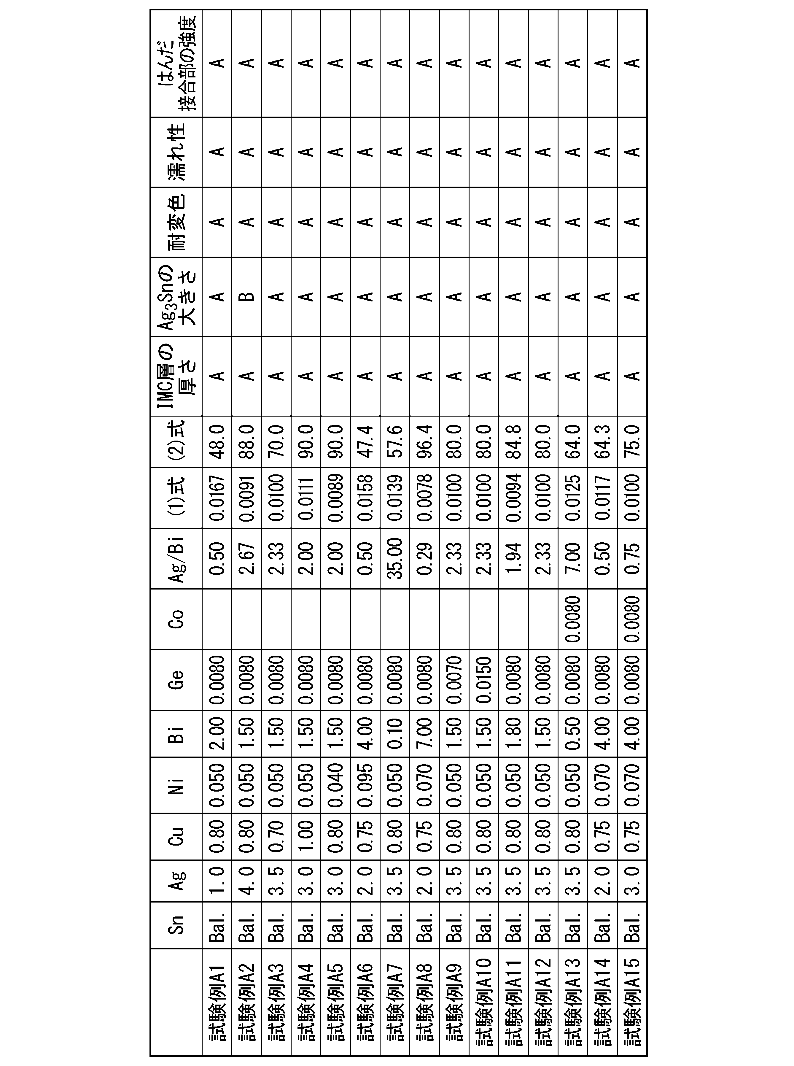

また、Cuの含有量が0.7~1.0質量%であり、かつ、Niの含有量が0.040~0.095質量%以下である、試験例B1~B2、試験例B7~B16は、IMC層の厚さの評価がAであった。
これに対して、Cu又はNiの含有量が上記範囲外である、試験例B3~B6は、IMC層の厚さの評価がBであった。
Agの含有量が、3.5質量%以下である、試験例A1、試験例A3~A14、試験例B1、試験例B3~B15は、Ag3Snの大きさの評価がAであった。
また、Agの含有量が、4.0質量%である、試験例A2、試験例B16は、Ag3Snの大きさの評価がBであった。
これに対して、Agの含有量が、4.0質量%超である、試験例B2は、Ag3Snの大きさの評価がCであった。
また、Geの含有量が、0.007質量%以上である、試験例B1~B8、試験例B10~B12は、耐変色の評価がAであった。
これに対して、Geの含有量が、0.007質量%未満である、試験例B9、B13~B16は、耐変色の評価がBであった。
また、試験例B2~B3、B5、B8~B9は、濡れ性の評価がAであった。
これに対して、0.017≦Ni/(Ag+Bi)であり、(Cu/Ni)×(Ag+Bi)≦46である、試験例B1、試験例B6、試験例B11~B13は、濡れ性の評価がBであった。
また、Cuの含有量が1.0質量%超である、試験例B4は、濡れ性の評価がBであった。
また、Biの含有量が0.1質量%未満である、試験例B7は、濡れ性の評価がBであった。
また、Geの含有量が0.015質量%超である、試験例B10は、濡れ性の評価がBであった。
また、Ag又はBiの含有量が十分ではない、試験例B14は、濡れ性の評価がBであった。
また、Ag:1.0~4.0質量%、Cu:0.7~1.0質量%、Bi:0.1~7.0質量%、Ni:0.040~0.095質量%、Ge:0.015質量%以下である、試験例B1~B8、試験例B9、試験例B11~B16は、はんだ接合部の強度の評価がAであった。
これに対して、Agの含有量が上記範囲外である、試験例B1、B2は、はんだ接合部の強度の評価がBであった。
また、Cuの含有量が上記範囲外である、試験例B3、B4は、はんだ接合部の強度の評価がBであった。
また、Niの含有量が上記範囲外である、試験例B5、B6は、はんだ接合部の強度の評価がBであった。
また、Biの含有量が所定の範囲外である、試験例B7、B8は、はんだ接合部の強度の評価がBであった。
また、Geの含有量が0.015質量%超である、試験例B10は、はんだ接合部の強度の評価がBであった。
前記はんだ合金は、接合界面における金属間化合物層の厚さを薄くすることができる。
また、前記はんだ合金は、微細なAg3Snを十分に析出させることができ、かつ、粗大なAg3Snの析出量を低減させることができる。
また、第5実施形態のはんだ合金は、合金の変色を抑制することができる。
また、第5実施形態のはんだ合金は、はんだ付け後の接合部の強度を高めることができる。
前記はんだ合金は、濡れ性を向上することができる。
試験例A1~A15は、融点が230℃近傍であり、引張強度が50MPa以上であった。


Claims (43)
- Ag:1.0~4.0質量%、Cu:0.1~1.0質量%、Bi:0.1~9.0質量%、Ni:0.005~0.3質量%、Ge:0.001~0.015質量%、及び、残部がSnからなる合金組成を有する、鉛フリーかつアンチモンフリーのはんだ合金。
- 前記合金組成は、Ag:1.0~3.5質量%である、請求項1に記載のはんだ合金。
- 前記合金組成は、Ag:2.0~3.5質量%である、請求項1又は2に記載のはんだ合金。
- 前記合金組成は、Ag:3.0~3.5質量%である、請求項1~3のいずれか一項に記載のはんだ合金。
- 前記合金組成は、Cu:0.5~0.85質量%である、請求項1~4のいずれか一項に記載のはんだ合金。
- 前記合金組成は、Cu:0.7~0.8質量%である、請求項1~5のいずれか一項に記載のはんだ合金。
- 前記合金組成は、Cu:0.75~0.8質量%である、請求項1~6のいずれか一項に記載のはんだ合金。
- 前記合金組成は、Bi:0.2~5.0質量%である、請求項1~7のいずれか一項に記載のはんだ合金。
- 前記合金組成は、Bi:0.5~4.0質量%である、請求項1~8のいずれか一項に記載のはんだ合金。
- 前記合金組成は、Bi:1.0~3.0質量%である、請求項1~9のいずれか一項に記載のはんだ合金。
- 前記合金組成は、Ni:0.02~0.09質量%である、請求項1~10のいずれか一項に記載のはんだ合金。
- 前記合金組成は、Ni:0.03~0.08質量%である、請求項1~11のいずれか一項に記載のはんだ合金。
- 前記合金組成は、Ni:0.04~0.06質量%である、請求項1~12のいずれか一項に記載のはんだ合金。
- 前記合金組成は、Ge:0.002~0.012質量%である、請求項1~13のいずれか一項に記載のはんだ合金。
- 前記合金組成は、Ge:0.003~0.01質量%である、請求項1~14のいずれか一項に記載のはんだ合金。
- 前記合金組成は、Ge:0.003~0.009質量%である、請求項1~15のいずれか一項に記載のはんだ合金。
- 更に、前記合金組成は、0.3≦Ag/Bi≦3.0を満たす、請求項1~16のいずれか一項に記載のはんだ合金。
Ag及びBiは各々前記合金組成での含有量(質量%)を表す。 - 更に、前記合金組成は、Co:0.001~0.1質量%を含有する、請求項1~16のいずれか一項に記載のはんだ合金。
- 前記合金組成は、Co:0.002~0.015質量%である、請求項18に記載のはんだ合金。
- 前記合金組成は、Co:0.004~0.012質量%である、請求項18又は19に記載のはんだ合金。
- 前記合金組成は、Co:0.006~0.009質量%である、請求項18~20のいずれか一項に記載のはんだ合金。
- 更に、前記合金組成は、1<Ag/Biを満たす、請求項1~17のいずれか一項に記載のはんだ合金。
Ag及びBiは各々前記合金組成での含有量(質量%)を表す。 - Ag:3.5質量%、Cu:0.8質量%、Bi:1.0~2.0質量%、Ni:0.05質量%、Ge:0.008質量%、及び、残部がSnからなる合金組成を有する、鉛フリーかつアンチモンフリーのはんだ合金。
- Ag:3.0~4.0質量%、Cu:0.7~0.9質量%、Bi:1.5質量%、Ni:0.03~0.08質量%、Ge:0.006~0.009質量%、及び、残部がSnからなる合金組成を有する、鉛フリーかつアンチモンフリーのはんだ合金。
- Ag:3.0~4.0質量%、Cu:0.7~0.9質量%、Bi:1.8質量%、Ni:0.03~0.08質量%、Ge:0.006~0.009質量%である、及び、残部がSnからなる合金組成を有する、鉛フリーかつアンチモンフリーのはんだ合金。
- 更に、前記合金組成は、1.2≦Ag/Bi≦3.0を満たす、請求項1~17、22~25のいずれか一項に記載のはんだ合金。
Ag及びBiは各々前記合金組成での含有量(質量%)を表す。 - 更に、前記合金組成は、Ag/Bi≦1を満たす、請求項1~17のいずれか一項に記載のはんだ合金。
Ag及びBiは各々前記合金組成での含有量(質量%)を表す。 - Ag:2.0質量%、Cu:0.8質量%、Bi:3.0~5.0質量%、Ni:0.05質量%、Ge:0.008質量%、及び、残部がSnからなる合金組成を有する、鉛フリーかつアンチモンフリーのはんだ合金。
- Ag:1.0~3.0質量%、Cu:0.7~0.9質量%、Bi:4.0質量%、Ni:0.04~0.08質量%、Ge:0.006~0.009質量%、及び、残部がSnからなる合金組成を有する、鉛フリーかつアンチモンフリーのはんだ合金。
- 更に、前記合金組成は、0.3≦Ag/Bi≦0.7を満たす、請求項1~17、27~29のいずれか一項に記載のはんだ合金。
Ag及びBiは各々前記合金組成での含有量(質量%)を表す。 - Ag:3.5質量%、Cu:0.8質量%、Bi:0.3~0.7質量%、Ni:0.05質量%、Ge:0.008質量%、Co:0.008質量%、及び、残部がSnからなる合金組成を有する、鉛フリーかつアンチモンフリーのはんだ合金。
- Ag:3.0~4.0質量%、Cu:0.7~0.9質量%、Bi:0.5質量%、Ni:0.03~0.08質量%、Ge:0.006~0.009質量%、Co:0.004~0.012質量%、及び、残部がSnからなる合金組成を有する、鉛フリーかつアンチモンフリーのはんだ合金。
- 前記合金組成は、Bi:0.3~1.0質量%であり、
更に、5≦Ag/Bi≦15を満たす、請求項18~21、31~32のいずれか一項に記載のはんだ合金。
Ag及びBiは各々前記合金組成での含有量(質量%)を表す。 - Ag:1.0~4.0質量%、Cu:0.7~1.0質量%、Bi:0.1~7.0質量%、Ni:0.040~0.095質量%、Ge:0.007~0.015質量%、及び、残部がSnからなる合金組成を有する、鉛フリーかつアンチモンフリーのはんだ合金。
- 更に、前記合金組成は、Co:0.001~0.1質量%を含有する、請求項34に記載のはんだ合金。
- 更に、0.007<Ni/(Ag+Bi)<0.017を満たす、請求項34又は35に記載のはんだ合金。
Ni、Ag及びBiは各々前記合金組成での含有量(質量%)を表す。 - 更に、46<(Cu/Ni)×(Ag+Bi)<120を満たす、請求項34~36のいずれか一項に記載のはんだ合金。
Cu、Ni、Ag及びBiは各々前記合金組成での含有量(質量%)を表す。 - 請求項1~37のいずれか一項に記載のはんだ合金からなるはんだボール。
- 平均粒径が1~1000μmである、請求項38に記載のはんだボール。
- 真球度が0.95以上である、請求項38又は39に記載のはんだボール。
- 真球度が0.99以上である、請求項38~40のいずれか一項に記載のはんだボール。
- 請求項38~41のいずれか一項に記載のはんだボールを用いて形成されたBall Grid Array。
- 請求項1~37のいずれか一項に記載のはんだ合金を用いてなるはんだ継手。
Priority Applications (12)
| Application Number | Priority Date | Filing Date | Title |
|---|---|---|---|
| KR1020237016199A KR102901735B1 (ko) | 2020-11-19 | 2021-11-17 | 땜납 합금, 땜납 볼, 및 땜납 이음 |
| JP2022517181A JP7100283B1 (ja) | 2020-11-19 | 2021-11-17 | はんだ合金、はんだボール、及びはんだ継手 |
| MYPI2023001946A MY199315A (en) | 2020-11-19 | 2021-11-17 | Solder alloy, solder ball and solder joint |
| EP24196170.5A EP4578592A1 (en) | 2020-11-19 | 2021-11-17 | Solder alloy, solder ball and solder joint |
| KR1020257041766A KR20260004560A (ko) | 2020-11-19 | 2021-11-17 | 땜납 합금, 땜납 볼, 및 땜납 이음 |
| US18/033,750 US12583060B2 (en) | 2020-11-19 | 2021-11-17 | Solder alloy, solder ball and solder joint |
| EP21894680.4A EP4249165A4 (en) | 2020-11-19 | 2021-11-17 | Solder alloy, solder ball and solder joint |
| MX2023005700A MX2023005700A (es) | 2020-11-19 | 2021-11-17 | Aleacion de soldadura, bola de soldadura y junta de soldadura. |
| CA3198256A CA3198256C (en) | 2020-11-19 | 2021-11-17 | WELDING ALLOY, WELDING GLOBE, AND SOFT BRAZING JOINT |
| CN202180077121.4A CN116472140A (zh) | 2020-11-19 | 2021-11-17 | 焊料合金、焊球及焊料接头 |
| JP2022097574A JP7144708B2 (ja) | 2020-11-19 | 2022-06-16 | はんだ合金、はんだボール、及びはんだ継手 |
| JP2022097573A JP2022130498A (ja) | 2020-11-19 | 2022-06-16 | はんだ合金、はんだボール、及びはんだ継手 |
Applications Claiming Priority (2)
| Application Number | Priority Date | Filing Date | Title |
|---|---|---|---|
| US202063115611P | 2020-11-19 | 2020-11-19 | |
| US63/115,611 | 2020-11-19 |
Publications (1)
| Publication Number | Publication Date |
|---|---|
| WO2022107806A1 true WO2022107806A1 (ja) | 2022-05-27 |
Family
ID=81708026
Family Applications (1)
| Application Number | Title | Priority Date | Filing Date |
|---|---|---|---|
| PCT/JP2021/042233 Ceased WO2022107806A1 (ja) | 2020-11-19 | 2021-11-17 | はんだ合金、はんだボール、及びはんだ継手 |
Country Status (10)
| Country | Link |
|---|---|
| US (1) | US12583060B2 (ja) |
| EP (2) | EP4578592A1 (ja) |
| JP (3) | JP7100283B1 (ja) |
| KR (2) | KR102901735B1 (ja) |
| CN (1) | CN116472140A (ja) |
| CA (3) | CA3198256C (ja) |
| MX (4) | MX2023005700A (ja) |
| MY (1) | MY199315A (ja) |
| TW (2) | TW202421803A (ja) |
| WO (1) | WO2022107806A1 (ja) |
Cited By (1)
| Publication number | Priority date | Publication date | Assignee | Title |
|---|---|---|---|---|
| US20230068294A1 (en) * | 2020-02-14 | 2023-03-02 | Senju Metal Industry Co., Ltd. | Lead-Free and Antimony-Free Solder Alloy, Solder Ball, and Solder Joint |
Families Citing this family (3)
| Publication number | Priority date | Publication date | Assignee | Title |
|---|---|---|---|---|
| JP7100283B1 (ja) * | 2020-11-19 | 2022-07-13 | 千住金属工業株式会社 | はんだ合金、はんだボール、及びはんだ継手 |
| TWI838983B (zh) * | 2022-11-28 | 2024-04-11 | 昇貿科技股份有限公司 | 無鉛銲料合金及焊料接點 |
| JP7633557B1 (ja) | 2023-12-28 | 2025-02-20 | 千住金属工業株式会社 | はんだ合金、はんだボール、はんだペースト、およびはんだ継手 |
Citations (8)
| Publication number | Priority date | Publication date | Assignee | Title |
|---|---|---|---|---|
| JP4144415B2 (ja) | 2003-01-07 | 2008-09-03 | 千住金属工業株式会社 | 鉛フリーはんだ |
| JP2014217888A (ja) * | 2013-05-03 | 2014-11-20 | 恒碩科技股▲ふん▼有限公司 | はんだ合金 |
| WO2015166945A1 (ja) * | 2014-04-30 | 2015-11-05 | 株式会社日本スペリア社 | 鉛フリーはんだ合金 |
| JP2018023987A (ja) * | 2016-08-09 | 2018-02-15 | 株式会社日本スペリア社 | 接合方法 |
| JP2018058090A (ja) * | 2016-10-06 | 2018-04-12 | 株式会社弘輝 | はんだペースト、はんだ合金粉 |
| JP6700568B1 (ja) * | 2019-08-09 | 2020-05-27 | 千住金属工業株式会社 | 鉛フリーかつアンチモンフリーのはんだ合金、はんだボール、Ball Grid Arrayおよびはんだ継手 |
| JP2021126686A (ja) * | 2020-02-14 | 2021-09-02 | 千住金属工業株式会社 | 鉛フリーかつアンチモンフリーのはんだ合金、はんだボール、およびはんだ継手 |
| JP2021178350A (ja) * | 2020-05-14 | 2021-11-18 | 株式会社日本スペリア社 | 鉛フリーはんだ合金 |
Family Cites Families (16)
| Publication number | Priority date | Publication date | Assignee | Title |
|---|---|---|---|---|
| JPH0670568A (ja) * | 1992-07-10 | 1994-03-11 | Matsushita Electric Ind Co Ltd | 直流モータの速度制御装置 |
| JP2000015476A (ja) * | 1998-06-29 | 2000-01-18 | Ishikawa Kinzoku Kk | 無鉛はんだ |
| US6517602B2 (en) * | 2000-03-14 | 2003-02-11 | Hitachi Metals, Ltd | Solder ball and method for producing same |
| US8562906B2 (en) * | 2006-03-09 | 2013-10-22 | Nippon Steel & Sumikin Materials Co., Ltd. | Lead-free solder alloy, solder ball and electronic member, and lead-free solder alloy, solder ball and electronic member for automobile-mounted electronic member |
| KR101243410B1 (ko) | 2007-07-13 | 2013-03-13 | 센주긴조쿠고교 가부시키가이샤 | 차재 실장용 무납 땜납과 차재 전자 회로 |
| EP2275224B1 (en) | 2008-04-23 | 2014-01-22 | Senju Metal Industry Co., Ltd | Lead-free solder alloy suppressed in occurrence of shrinkage cavity |
| CN101716703B (zh) | 2009-11-30 | 2012-11-21 | 南京达迈科技实业有限公司 | 低银SnAgCuBi系无铅焊锡合金及其制备方法 |
| US20150266137A1 (en) | 2012-10-09 | 2015-09-24 | Alpha Metals, Inc. | Lead-free and antimony-free tin solder reliable at high temperatures |
| US9320152B2 (en) | 2013-05-29 | 2016-04-19 | Nippon Steel & Sumikin Materials Co., Ltd. | Solder ball and electronic member |
| JP6145164B2 (ja) | 2013-09-11 | 2017-06-07 | 千住金属工業株式会社 | 鉛フリーはんだ、鉛フリーはんだボール、この鉛フリーはんだを使用したはんだ継手およびこのはんだ継手を有する半導体回路 |
| KR101985646B1 (ko) | 2014-07-21 | 2019-06-04 | 알파 어셈블리 솔루션스 인크. | 솔더링용 저온 고신뢰성 주석 합금 |
| US20180102464A1 (en) | 2016-10-06 | 2018-04-12 | Alpha Assembly Solutions Inc. | Advanced Solder Alloys For Electronic Interconnects |
| WO2018174162A1 (ja) | 2017-03-23 | 2018-09-27 | 株式会社日本スペリア社 | はんだ継手 |
| JP6578393B2 (ja) * | 2018-02-27 | 2019-09-18 | 株式会社タムラ製作所 | 鉛フリーはんだ合金、電子回路実装基板及び電子制御装置 |
| TWI725664B (zh) | 2018-12-14 | 2021-04-21 | 日商千住金屬工業股份有限公司 | 焊料合金、焊料膏、焊料預形體及焊料接頭 |
| JP7100283B1 (ja) * | 2020-11-19 | 2022-07-13 | 千住金属工業株式会社 | はんだ合金、はんだボール、及びはんだ継手 |
-
2021
- 2021-11-17 JP JP2022517181A patent/JP7100283B1/ja active Active
- 2021-11-17 EP EP24196170.5A patent/EP4578592A1/en active Pending
- 2021-11-17 CA CA3198256A patent/CA3198256C/en active Active
- 2021-11-17 CA CA3236527A patent/CA3236527A1/en active Pending
- 2021-11-17 MX MX2023005700A patent/MX2023005700A/es unknown
- 2021-11-17 WO PCT/JP2021/042233 patent/WO2022107806A1/ja not_active Ceased
- 2021-11-17 CA CA3236521A patent/CA3236521A1/en active Pending
- 2021-11-17 CN CN202180077121.4A patent/CN116472140A/zh active Pending
- 2021-11-17 TW TW113101418A patent/TW202421803A/zh unknown
- 2021-11-17 KR KR1020237016199A patent/KR102901735B1/ko active Active
- 2021-11-17 KR KR1020257041766A patent/KR20260004560A/ko active Pending
- 2021-11-17 MY MYPI2023001946A patent/MY199315A/en unknown
- 2021-11-17 EP EP21894680.4A patent/EP4249165A4/en active Pending
- 2021-11-17 US US18/033,750 patent/US12583060B2/en active Active
- 2021-11-17 TW TW110142774A patent/TWI833132B/zh active
-
2022
- 2022-06-16 JP JP2022097574A patent/JP7144708B2/ja active Active
- 2022-06-16 JP JP2022097573A patent/JP2022130498A/ja active Pending
-
2023
- 2023-05-15 MX MX2023014150A patent/MX2023014150A/es unknown
- 2023-05-15 MX MX2023011401A patent/MX2023011401A/es unknown
- 2023-05-15 MX MX2023011402A patent/MX2023011402A/es unknown
Patent Citations (8)
| Publication number | Priority date | Publication date | Assignee | Title |
|---|---|---|---|---|
| JP4144415B2 (ja) | 2003-01-07 | 2008-09-03 | 千住金属工業株式会社 | 鉛フリーはんだ |
| JP2014217888A (ja) * | 2013-05-03 | 2014-11-20 | 恒碩科技股▲ふん▼有限公司 | はんだ合金 |
| WO2015166945A1 (ja) * | 2014-04-30 | 2015-11-05 | 株式会社日本スペリア社 | 鉛フリーはんだ合金 |
| JP2018023987A (ja) * | 2016-08-09 | 2018-02-15 | 株式会社日本スペリア社 | 接合方法 |
| JP2018058090A (ja) * | 2016-10-06 | 2018-04-12 | 株式会社弘輝 | はんだペースト、はんだ合金粉 |
| JP6700568B1 (ja) * | 2019-08-09 | 2020-05-27 | 千住金属工業株式会社 | 鉛フリーかつアンチモンフリーのはんだ合金、はんだボール、Ball Grid Arrayおよびはんだ継手 |
| JP2021126686A (ja) * | 2020-02-14 | 2021-09-02 | 千住金属工業株式会社 | 鉛フリーかつアンチモンフリーのはんだ合金、はんだボール、およびはんだ継手 |
| JP2021178350A (ja) * | 2020-05-14 | 2021-11-18 | 株式会社日本スペリア社 | 鉛フリーはんだ合金 |
Non-Patent Citations (1)
| Title |
|---|
| See also references of EP4249165A4 |
Cited By (2)
| Publication number | Priority date | Publication date | Assignee | Title |
|---|---|---|---|---|
| US20230068294A1 (en) * | 2020-02-14 | 2023-03-02 | Senju Metal Industry Co., Ltd. | Lead-Free and Antimony-Free Solder Alloy, Solder Ball, and Solder Joint |
| US12377500B2 (en) * | 2020-02-14 | 2025-08-05 | Senju Metal Industry Co., Ltd. | Lead-free and antimony-free solder alloy, solder ball, and solder joint |
Also Published As
| Publication number | Publication date |
|---|---|
| KR20230087565A (ko) | 2023-06-16 |
| MX2023011402A (es) | 2023-10-12 |
| CN116472140A (zh) | 2023-07-21 |
| JP2022126750A (ja) | 2022-08-30 |
| KR102901735B1 (ko) | 2025-12-19 |
| JP7100283B1 (ja) | 2022-07-13 |
| JP2022130498A (ja) | 2022-09-06 |
| US12583060B2 (en) | 2026-03-24 |
| EP4249165A4 (en) | 2024-05-15 |
| EP4249165A1 (en) | 2023-09-27 |
| TW202421803A (zh) | 2024-06-01 |
| MX2023011401A (es) | 2023-10-12 |
| TWI833132B (zh) | 2024-02-21 |
| EP4578592A1 (en) | 2025-07-02 |
| MY199315A (en) | 2023-10-24 |
| US20230398643A1 (en) | 2023-12-14 |
| MX2023005700A (es) | 2023-11-30 |
| KR20260004560A (ko) | 2026-01-08 |
| JPWO2022107806A1 (ja) | 2022-05-27 |
| CA3236527A1 (en) | 2022-05-27 |
| CA3198256A1 (en) | 2022-05-27 |
| CA3198256C (en) | 2025-05-06 |
| CA3236521A1 (en) | 2022-05-27 |
| MX2023014150A (es) | 2023-12-13 |
| TW202229570A (zh) | 2022-08-01 |
| JP7144708B2 (ja) | 2022-09-30 |
Similar Documents
| Publication | Publication Date | Title |
|---|---|---|
| JP7100283B1 (ja) | はんだ合金、はんだボール、及びはんだ継手 | |
| KR102498103B1 (ko) | 납 프리 및 안티몬 프리의 땜납 합금, 땜납 볼, 볼 그리드 어레이 그리고 솔더 조인트 | |
| KR102543492B1 (ko) | 납 프리 또한 안티몬 프리의 땜납 합금, 땜납 볼 및 땜납 이음 | |
| JP7025679B2 (ja) | 鉛フリーかつアンチモンフリーのはんだ合金、はんだボール、およびはんだ継手 | |
| HK40089440A (zh) | 焊料合金、焊球及焊料接头 | |
| BR122024003180B1 (pt) | Liga de solda, esfera de solda, matriz de grade de esferas e junta de solda | |
| BR112023007162B1 (pt) | Liga de solda, esfera de solda, matriz de grade de esferas e junta de solda | |
| BR122024003180A2 (pt) | Liga de solda, esfera de solda e junta de solda | |
| HK40066658B (en) | Lead-free and antimony-free solder alloy, solder ball, ball grid array, and solder joint | |
| HK40066658A (en) | Lead-free and antimony-free solder alloy, solder ball, ball grid array, and solder joint |
Legal Events
| Date | Code | Title | Description |
|---|---|---|---|
| ENP | Entry into the national phase |
Ref document number: 2022517181 Country of ref document: JP Kind code of ref document: A |
|
| 121 | Ep: the epo has been informed by wipo that ep was designated in this application |
Ref document number: 21894680 Country of ref document: EP Kind code of ref document: A1 |
|
| REG | Reference to national code |
Ref country code: BR Ref legal event code: B01A Ref document number: 112023007162 Country of ref document: BR |
|
| WWE | Wipo information: entry into national phase |
Ref document number: 202337032754 Country of ref document: IN |
|
| ENP | Entry into the national phase |
Ref document number: 3198256 Country of ref document: CA |
|
| ENP | Entry into the national phase |
Ref document number: 20237016199 Country of ref document: KR Kind code of ref document: A |
|
| WWE | Wipo information: entry into national phase |
Ref document number: 202180077121.4 Country of ref document: CN |
|
| ENP | Entry into the national phase |
Ref document number: 112023007162 Country of ref document: BR Kind code of ref document: A2 Effective date: 20230417 |
|
| NENP | Non-entry into the national phase |
Ref country code: DE |
|
| ENP | Entry into the national phase |
Ref document number: 2021894680 Country of ref document: EP Effective date: 20230619 |
|
| WWG | Wipo information: grant in national office |
Ref document number: 202337032754 Country of ref document: IN |
|
| WWD | Wipo information: divisional of initial pct application |
Ref document number: 1020257041766 Country of ref document: KR |
|
| WWP | Wipo information: published in national office |
Ref document number: 1020257041766 Country of ref document: KR |
|
| WWG | Wipo information: grant in national office |
Ref document number: 18033750 Country of ref document: US |