WO2022118510A1 - 絶縁基板および電力変換装置 - Google Patents
絶縁基板および電力変換装置 Download PDFInfo
- Publication number
- WO2022118510A1 WO2022118510A1 PCT/JP2021/032188 JP2021032188W WO2022118510A1 WO 2022118510 A1 WO2022118510 A1 WO 2022118510A1 JP 2021032188 W JP2021032188 W JP 2021032188W WO 2022118510 A1 WO2022118510 A1 WO 2022118510A1
- Authority
- WO
- WIPO (PCT)
- Prior art keywords
- conductor
- conductors
- insulating
- insulating plate
- insulating substrate
- Prior art date
- Legal status (The legal status is an assumption and is not a legal conclusion. Google has not performed a legal analysis and makes no representation as to the accuracy of the status listed.)
- Ceased
Links
Images








Classifications
-
- H—ELECTRICITY
- H10—SEMICONDUCTOR DEVICES; ELECTRIC SOLID-STATE DEVICES NOT OTHERWISE PROVIDED FOR
- H10W—GENERIC PACKAGES, INTERCONNECTIONS, CONNECTORS OR OTHER CONSTRUCTIONAL DETAILS OF DEVICES COVERED BY CLASS H10
- H10W40/00—Arrangements for thermal protection or thermal control
- H10W40/20—Arrangements for cooling
- H10W40/25—Arrangements for cooling characterised by their materials
- H10W40/255—Arrangements for cooling characterised by their materials having a laminate or multilayered structure, e.g. direct bond copper [DBC] ceramic substrates
-
- H—ELECTRICITY
- H10—SEMICONDUCTOR DEVICES; ELECTRIC SOLID-STATE DEVICES NOT OTHERWISE PROVIDED FOR
- H10W—GENERIC PACKAGES, INTERCONNECTIONS, CONNECTORS OR OTHER CONSTRUCTIONAL DETAILS OF DEVICES COVERED BY CLASS H10
- H10W40/00—Arrangements for thermal protection or thermal control
- H10W40/20—Arrangements for cooling
- H10W40/22—Arrangements for cooling characterised by their shape, e.g. having conical or cylindrical projections
- H10W40/226—Arrangements for cooling characterised by their shape, e.g. having conical or cylindrical projections characterised by projecting parts, e.g. fins to increase surface area
- H10W40/228—Arrangements for cooling characterised by their shape, e.g. having conical or cylindrical projections characterised by projecting parts, e.g. fins to increase surface area the projecting parts being wire-shaped or pin-shaped
-
- H—ELECTRICITY
- H10—SEMICONDUCTOR DEVICES; ELECTRIC SOLID-STATE DEVICES NOT OTHERWISE PROVIDED FOR
- H10W—GENERIC PACKAGES, INTERCONNECTIONS, CONNECTORS OR OTHER CONSTRUCTIONAL DETAILS OF DEVICES COVERED BY CLASS H10
- H10W44/00—Electrical arrangements for controlling or matching impedance
- H10W44/501—Inductive arrangements
-
- H—ELECTRICITY
- H10—SEMICONDUCTOR DEVICES; ELECTRIC SOLID-STATE DEVICES NOT OTHERWISE PROVIDED FOR
- H10W—GENERIC PACKAGES, INTERCONNECTIONS, CONNECTORS OR OTHER CONSTRUCTIONAL DETAILS OF DEVICES COVERED BY CLASS H10
- H10W90/00—Package configurations
-
- H—ELECTRICITY
- H02—GENERATION; CONVERSION OR DISTRIBUTION OF ELECTRIC POWER
- H02M—APPARATUS FOR CONVERSION BETWEEN AC AND AC, BETWEEN AC AND DC, OR BETWEEN DC AND DC, AND FOR USE WITH MAINS OR SIMILAR POWER SUPPLY SYSTEMS; CONVERSION OF DC OR AC INPUT POWER INTO SURGE OUTPUT POWER; CONTROL OR REGULATION THEREOF
- H02M1/00—Details of apparatus for conversion
- H02M1/32—Means for protecting converters other than automatic disconnection
- H02M1/327—Means for protecting converters other than automatic disconnection against abnormal temperatures
-
- H—ELECTRICITY
- H02—GENERATION; CONVERSION OR DISTRIBUTION OF ELECTRIC POWER
- H02M—APPARATUS FOR CONVERSION BETWEEN AC AND AC, BETWEEN AC AND DC, OR BETWEEN DC AND DC, AND FOR USE WITH MAINS OR SIMILAR POWER SUPPLY SYSTEMS; CONVERSION OF DC OR AC INPUT POWER INTO SURGE OUTPUT POWER; CONTROL OR REGULATION THEREOF
- H02M7/00—Conversion of AC power input into DC power output; Conversion of DC power input into AC power output
- H02M7/003—Constructional details, e.g. physical layout, assembly, wiring or busbar connections
-
- H—ELECTRICITY
- H10—SEMICONDUCTOR DEVICES; ELECTRIC SOLID-STATE DEVICES NOT OTHERWISE PROVIDED FOR
- H10W—GENERIC PACKAGES, INTERCONNECTIONS, CONNECTORS OR OTHER CONSTRUCTIONAL DETAILS OF DEVICES COVERED BY CLASS H10
- H10W70/00—Package substrates; Interposers; Redistribution layers [RDL]
- H10W70/60—Insulating or insulated package substrates; Interposers; Redistribution layers
- H10W70/611—Insulating or insulated package substrates; Interposers; Redistribution layers for connecting multiple chips together
-
- H—ELECTRICITY
- H10—SEMICONDUCTOR DEVICES; ELECTRIC SOLID-STATE DEVICES NOT OTHERWISE PROVIDED FOR
- H10W—GENERIC PACKAGES, INTERCONNECTIONS, CONNECTORS OR OTHER CONSTRUCTIONAL DETAILS OF DEVICES COVERED BY CLASS H10
- H10W70/00—Package substrates; Interposers; Redistribution layers [RDL]
- H10W70/60—Insulating or insulated package substrates; Interposers; Redistribution layers
- H10W70/62—Insulating or insulated package substrates; Interposers; Redistribution layers characterised by their interconnections
- H10W70/65—Shapes or dispositions of interconnections
-
- H—ELECTRICITY
- H10—SEMICONDUCTOR DEVICES; ELECTRIC SOLID-STATE DEVICES NOT OTHERWISE PROVIDED FOR
- H10W—GENERIC PACKAGES, INTERCONNECTIONS, CONNECTORS OR OTHER CONSTRUCTIONAL DETAILS OF DEVICES COVERED BY CLASS H10
- H10W72/00—Interconnections or connectors in packages
- H10W72/50—Bond wires
- H10W72/531—Shapes of wire connectors
- H10W72/5363—Shapes of wire connectors the connected ends being wedge-shaped
-
- H—ELECTRICITY
- H10—SEMICONDUCTOR DEVICES; ELECTRIC SOLID-STATE DEVICES NOT OTHERWISE PROVIDED FOR
- H10W—GENERIC PACKAGES, INTERCONNECTIONS, CONNECTORS OR OTHER CONSTRUCTIONAL DETAILS OF DEVICES COVERED BY CLASS H10
- H10W74/00—Encapsulations, e.g. protective coatings
-
- H—ELECTRICITY
- H10—SEMICONDUCTOR DEVICES; ELECTRIC SOLID-STATE DEVICES NOT OTHERWISE PROVIDED FOR
- H10W—GENERIC PACKAGES, INTERCONNECTIONS, CONNECTORS OR OTHER CONSTRUCTIONAL DETAILS OF DEVICES COVERED BY CLASS H10
- H10W74/00—Encapsulations, e.g. protective coatings
- H10W74/10—Encapsulations, e.g. protective coatings characterised by their shape or disposition
- H10W74/111—Encapsulations, e.g. protective coatings characterised by their shape or disposition the semiconductor body being completely enclosed
-
- H—ELECTRICITY
- H10—SEMICONDUCTOR DEVICES; ELECTRIC SOLID-STATE DEVICES NOT OTHERWISE PROVIDED FOR
- H10W—GENERIC PACKAGES, INTERCONNECTIONS, CONNECTORS OR OTHER CONSTRUCTIONAL DETAILS OF DEVICES COVERED BY CLASS H10
- H10W74/00—Encapsulations, e.g. protective coatings
- H10W74/10—Encapsulations, e.g. protective coatings characterised by their shape or disposition
- H10W74/111—Encapsulations, e.g. protective coatings characterised by their shape or disposition the semiconductor body being completely enclosed
- H10W74/114—Encapsulations, e.g. protective coatings characterised by their shape or disposition the semiconductor body being completely enclosed by a substrate and the encapsulations
-
- H—ELECTRICITY
- H10—SEMICONDUCTOR DEVICES; ELECTRIC SOLID-STATE DEVICES NOT OTHERWISE PROVIDED FOR
- H10W—GENERIC PACKAGES, INTERCONNECTIONS, CONNECTORS OR OTHER CONSTRUCTIONAL DETAILS OF DEVICES COVERED BY CLASS H10
- H10W76/00—Containers; Fillings or auxiliary members therefor; Seals
- H10W76/10—Containers or parts thereof
- H10W76/12—Containers or parts thereof characterised by their shape
- H10W76/13—Containers comprising a conductive base serving as an interconnection
- H10W76/138—Containers comprising a conductive base serving as an interconnection having another interconnection being formed by a cover plate parallel to the conductive base, e.g. sandwich type
-
- H—ELECTRICITY
- H10—SEMICONDUCTOR DEVICES; ELECTRIC SOLID-STATE DEVICES NOT OTHERWISE PROVIDED FOR
- H10W—GENERIC PACKAGES, INTERCONNECTIONS, CONNECTORS OR OTHER CONSTRUCTIONAL DETAILS OF DEVICES COVERED BY CLASS H10
- H10W90/00—Package configurations
- H10W90/701—Package configurations characterised by the relative positions of pads or connectors relative to package parts
- H10W90/751—Package configurations characterised by the relative positions of pads or connectors relative to package parts of bond wires
- H10W90/754—Package configurations characterised by the relative positions of pads or connectors relative to package parts of bond wires between a chip and a stacked insulating package substrate, interposer or RDL
Definitions
- the present invention relates to an insulating substrate and a power conversion device, and more particularly to an insulating substrate for mounting a semiconductor chip and a power conversion device using the insulating substrate.
- a power semiconductor chip such as SiC or GaN can be driven at a high frequency, it is possible to reduce the size of passive components such as an inductor or a capacitor included in a power conversion device. Due to these effects, it is possible to reduce the overall size of the power converter.
- the parasitic inductance Ls of the power converter becomes an issue.
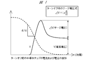
- the surge voltage ⁇ V is represented by the product of the parasitic inductance Ls and the amount of current (di / dt) per unit time.
- the large parasitic inductance Ls causes a large surge voltage ⁇ V to be applied when the semiconductor chip is turned off, and is also a source of noise. Further, in order to drive at high frequencies, it is necessary to increase the off-speed of the semiconductor chip, but the surge voltage ⁇ V and noise have a great influence on the off-speed.
- Patent Document 1 discloses an insulating substrate including an insulating plate, a front surface wiring conductor formed on the surface of the insulating plate, and a back surface wiring conductor formed on the back surface of the insulating plate. A semiconductor chip is installed on the surface wiring conductor.
- Patent Document 1 discloses a technique for reducing parasitic inductance by the effect of proximity reverse flow by using a bridge terminal provided on a surface wiring conductor.
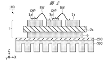
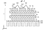
- the inventors of the present application examined the structures of Study Example 1 shown in FIG. 2 and Study Example 2 shown in FIG. 3 as a power conversion device 100 for a compound semiconductor substrate.
- the insulating plate 2a, the plurality of conductors 3a formed on the surface of the insulating plate 2a, and the heat dissipation conductivity formed on the back surface of the insulating plate 2a As shown in FIG. 2, in the power conversion device 100 of Study Example 1, the insulating plate 2a, the plurality of conductors 3a formed on the surface of the insulating plate 2a, and the heat dissipation conductivity formed on the back surface of the insulating plate 2a.
- the insulating substrate 1 provided with the body 5 is used.
- a plurality of semiconductor chip CHPs are installed on the plurality of conductors 3a, and the plurality of conductors 3a and the plurality of semiconductor chip CHPs are appropriately electrically connected by a bonding wire BW. Further, the heat radiating conductor 5 is connected to the heat sink 300 via the base plate 200.
- the power conversion device 100 of Study Example 2 further includes a conductor 3b and an insulating plate 2b between the insulating plate 2a and the heat radiating conductor 5, and has a multilayer insulating substrate structure. It is made up. Therefore, in Study Example 2, since the insulating plate and the conductor through which the current flows are laminated over several layers, the parasitic inductance Ls can be reduced by the mutual inductance as compared with Study Example 1. ..
- the insulating substrate includes a first insulating plate having a front surface and a back surface, a second insulating plate formed on the back surface side of the first insulating plate and having a front surface and a back surface, and the first insulating plate.
- a plurality of first conductors formed on the front surface of the plate, a second conductor formed between the back surface of the first insulating plate and the front surface of the second insulating plate, and the back surface of the second insulating plate.
- the first conductor is formed in the above direction and electrically insulated from the second conductor, and a part of the plurality of first conductors and the second conductor are electrically connected to each other.
- a plurality of first connecting conductors formed inside the insulating plate are provided.
- the plurality of first conductors include a first unconnected conductor that is not electrically connected to the second conductor via the plurality of first connecting conductors, and the first insulating plate. Is embedded in the first insulating plate and a protruding conductor is formed so as to project from the back surface of the first insulating plate, and the protruding conductor is formed on the first unconnected conductor. It is electrically connected and is electrically insulated from the second conductor and the heat radiating conductor.
- the insulating substrate according to the embodiment is formed on a first insulating plate having a front surface and a back surface, a plurality of first conductors formed on the surface of the first insulating plate, and the back surface of the first insulating plate. Formed inside the first insulating plate so as to electrically connect the formed plurality of second conductors, a part of the plurality of first conductors, and a part of the plurality of second conductors. It is provided with a plurality of first connection conductors.
- the plurality of second conductors include a second unconnected conductor that is electrically insulated from the other second conductor, and the second unconnected conductor includes the first insulating plate.
- the heat radiating conductor is connected so as to protrude from the other second conductor on the back surface side of the above.
- an insulating substrate capable of keeping the parasitic inductance low and improving heat dissipation. Further, by using such an insulating substrate, the reliability of the power conversion device can be improved.
- FIG. 1 It is a graph for demonstrating the surge voltage at the time of turn-off. It is sectional drawing which shows the insulation substrate and the power conversion apparatus in Study Example 1. FIG. It is sectional drawing which shows the insulation substrate and the power conversion apparatus in Study Example 2. It is a perspective view which shows the insulating substrate in Embodiment 1. FIG. It is sectional drawing which shows the insulation substrate in Embodiment 1. FIG. It is a top view which shows the inside of the insulating substrate in Embodiment 1. FIG. It is a top view which shows the inside of the insulating substrate in Embodiment 1. FIG. It is a perspective view which shows the power conversion apparatus in Embodiment 1. FIG. It is sectional drawing which shows the power conversion apparatus in Embodiment 1. FIG.
- FIG. 1 It is a graph which shows the effect of Embodiment 1 and Embodiment 3. It is a graph which shows the effect of Embodiment 1 and Embodiment 3. It is sectional drawing which shows the insulation substrate in Embodiment 2.
- FIG. It is sectional drawing which shows the insulation substrate in Embodiment 3.
- FIG. 1 It is a graph which shows the effect of Embodiment 1 and Embodiment 3.
- FIG. It is sectional drawing which shows the insulation substrate in Embodiment 2.
- FIG. It is sectional drawing which shows the insulation substrate in Embodi
- FIG. It is a top view which shows the inside of the insulating substrate in Embodiment 4.
- FIG. It is sectional drawing which shows the insulation substrate in Embodiment 4.
- FIG. It is sectional drawing which shows the insulation substrate in Embodiment 4.
- FIG. It is sectional drawing which shows the power conversion apparatus in Embodiment 4.
- the X, Y, and Z directions described in the present application intersect each other and are orthogonal to each other.
- the Z direction is described as the vertical direction, the vertical direction, the height direction, or the thickness direction of a certain structure.
- the expression "planar view" used in the present application means that a surface composed of the X direction and the Y direction is viewed from the Z direction.
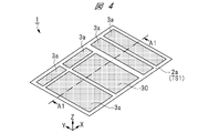
- FIG. 4 is a perspective view showing the insulating substrate 1
- FIG. 5 is a cross-sectional view taken along the line A1-A1 shown in FIG. 6 and 7 are plan views showing the layer of the conductor 3b in the insulating substrate 1.
- the insulating substrate 1 has a multilayer insulating substrate structure in which an insulating plate and a conductor through which an electric current flows are laminated over several layers.
- the insulating substrate 1 includes an insulating plate 2a, an insulating plate 2b, a plurality of conductors 3a, a conductor 3b, a plurality of connecting conductors 4a, and a heat radiating conductor 5.
- the insulating plate 2a has a front surface TS1 and a back surface BS1. As shown in FIG. 4, a plurality of conductors 3a are formed on the surface TS1 of the insulating plate 2a. Further, the plurality of conductors 3a include the unconnected conductor 30.
- the insulating plate 2b is formed on the back surface BS1 side of the insulating plate 2a and has a front surface TS2 and a back surface BS2.
- a conductor 3b is formed between the back surface BS1 of the insulating plate 2a and the front surface TS2 of the insulating plate 2b.
- a plurality of connecting conductors 4a are formed so as to electrically connect a part of the plurality of conductors 3a and the conductors 3b.
- a heat radiating conductor 5 electrically insulated from the conductor 3b is formed on the back surface BS2 of the insulating plate 2b.
- various electronic devices such as a plurality of semiconductor chips, capacitors and inductors are installed in the plurality of conductors 3a, and the plurality of conductors 3a, the plurality of connected conductors 4a and the conductors 3b are provided. By being electrically connected, electrical conduction is established between the electronic devices, and a current path is constructed.
- a plurality of conductors 3b may be provided. In that case, a more complicated circuit can be constructed by the plurality of conductors 3b.
- the parasitic inductance Ls can be reduced by the mutual inductance.
- the insulating substrate 1 has a multilayer insulating substrate structure, so that between the plurality of semiconductor chips and the heat radiating conductor 5. There is a problem that the distance becomes long and the heat dissipation tends to decrease.
- the plurality of conductors 3a include an unconnected conductor 30 that is not electrically connected to the conductor 3b via the plurality of connected conductors 4a.
- a protruding conductor 40 is formed so as to be embedded inside the insulating plate 2a and protrude from the back surface BS1 of the insulating plate 2a.
- the protruding conductor 40 is electrically connected to the unconnected conductor 30 and is electrically insulated from the heat radiating conductor 5 by the insulating plate 2b.
- the protruding conductor 40 is electrically insulated from the conductor 3b by the insulating layer 41 surrounding the protruding conductor 40 in a plan view.
- the parasitic inductance Ls can be kept low and the heat dissipation can be improved.
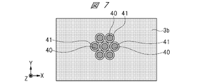
- the protruding conductor 40 may be provided not only as one as shown in FIG. 6 but also as a plurality as shown in FIG. 7.
- a plurality of protruding conductors 40 are formed on the insulating plate 2a.
- Each of the plurality of projecting conductors 40 is electrically connected to the unconnected conductor 30, electrically insulated from the conductor 3b by the insulating layer 41, and electrically insulated from the heat radiating conductor 5 by the insulating plate 2b. ing.
- each protruding conductor 40 is smaller than that of FIG. 6, but if the total flat area of the plurality of protruding conductors 40 is designed to be about the same as that of FIG. 6, the figure is shown. Even in 7, the same level of heat dissipation as in FIG. 6 can be secured.
- the plurality of conductors 3a including the unconnected conductor 30, the conductor 3b, the heat radiating conductor 5, the plurality of connected conductors 4a, and the protruding conductor 40 are, for example, copper (Cu) or aluminum. It is made of a metallic material containing (Al). Further, the insulating plate 2a and the insulating plate 2b are made of, for example, a ceramic or a resin material.
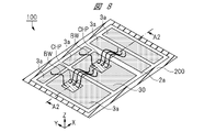
- FIG. 8 is a perspective view showing the power conversion device 100
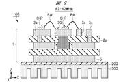
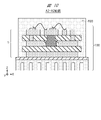
- FIGS. 9 and 10 are cross-sectional views taken along the line A2-A2 shown in FIG.
- the A2-A2 line is located on the same straight line as the A1-A1 line shown in FIGS. 4 and 6.
- the power conversion device 100 includes an insulating substrate 1, a plurality of semiconductor chip CHPs, a bonding wire BW, a base plate 200, and a heat sink 300.
- the heat sink 300 is connected to the heat dissipation conductor 5 via the base plate 200.
- the heat-dissipating conductor 5 and the base plate 200 are connected via a TIM (Thermal interface material).
- the base plate 200 and the heat sink 300 are also connected via the TIM.
- TIM is a material such as, for example, solder or sintered material.
- the plurality of semiconductor chip CHPs have a front surface and a back surface, respectively, and the back surface of each of the plurality of semiconductor chip CHPs is installed on the plurality of conductors 3a by TIM. Further, at least one of the plurality of semiconductor chip CHPs is provided on the unconnected conductor 30.
- the plurality of semiconductor chip CHPs and the plurality of conductors 3a are appropriately electrically connected by the bonding wire BW.
- capacitors and inductors may be installed on the plurality of conductors 3a in addition to the plurality of semiconductor chip CHPs.
- the insulating substrate 1, the plurality of semiconductor chip CHPs, and the bonding wire BW may be covered with the protective member 400.
- the protective member 400 is made of an insulating material, for example, an insulating gel or a mold resin.
- the semiconductor chip CHP includes, for example, a compound semiconductor substrate such as silicon carbide (SiC), gallium nitride (GaN) or gallium oxide (Ga 2 O 3 ), and a transistor such as a MOSFET formed on the compound semiconductor substrate. And include.
- a compound semiconductor substrate such as silicon carbide (SiC), gallium nitride (GaN) or gallium oxide (Ga 2 O 3 ), and a transistor such as a MOSFET formed on the compound semiconductor substrate. And include.
- the bonding wire BW is made of a metal material containing, for example, gold (Au), copper (Cu) or aluminum (Al). Further, instead of the bonding wire BW, a plurality of semiconductor chip CHPs and a plurality of conductors 3a may be electrically connected by a ribbon, a bus bar, or the like.
- the base plate 200 is made of, for example, a composite material (AlSiC) containing SiC ceramic particles in an aluminum alloy or a composite material (MgSiC) containing SiC ceramic particles in magnesium.
- the heat sink 300 is made of, for example, a metal material containing copper (Cu), iron (Fe) or aluminum.
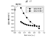
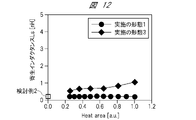
- FIGS. 11 and 12 are graphs showing the effect of the first embodiment, and are simulation results measured by the inventors of the present application. It should be noted that FIGS. 11 and 12 also show the effects of the third embodiment described later. Further, the “Heat area” on the horizontal axis of FIGS. 11 and 12 indicates the area of the protruding conductor 40 in a plan view in the first embodiment.
- the temperature rise can be suppressed as compared with the study example 2 (FIG. 3), and the parasitic inductance Ls is examined in the study example 2 (FIG. 3). It can be kept at the same level as in Fig. 3). That is, according to the first embodiment, it is possible to provide an insulating substrate 1 capable of keeping the parasitic inductance Ls low and enhancing heat dissipation, and by using such an insulating substrate 1, the reliability of the power conversion device 100 can be provided. Can be improved.
- the insulating substrate 1 in the second embodiment has a multilayer insulating substrate structure in which more insulating plates and conductors are laminated between the insulating plate 2b and the heat radiating conductor 5 as compared with the first embodiment. ing.
- an insulating plate 2c having a front surface TS3 and a back surface BS3 is formed between the insulating plate 2b and the heat radiating conductor 5.
- the conductor 3c is formed between the back surface BS2 of the insulating plate 2b and the front surface TS3 of the insulating plate 2c.
- a plurality of connecting conductors 4b are formed so as to electrically connect the conductor 3b and the conductor 3c.
- the protruding conductor 40 penetrates the insulating plate 2b, protrudes from the back surface of the insulating plate 2b, and is electrically insulated from the conductor 3c and the connecting conductor 4b.
- the structure including the insulating plate 2c, the conductor 3c, the plurality of connecting conductors 4b, and the protruding conductor 40 is formed once or more from the insulating plate 2b to the heat radiating conductor 5. It is repeatedly formed. For example, when the above structure is repeated twice, the conductor 3d and the connecting conductor 4c shown in FIG. 13 are formed.
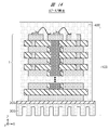
- FIG. 14 shows a power conversion device 100 using the insulating substrate 1 in the second embodiment.
- the insulating substrate 1, the plurality of semiconductor chips CHP, and the bonding wire BW, which are further multi-layered, may be covered with the protective member 400.
- Various electronic devices such as a plurality of semiconductor chip CHPs, capacitors, and inductors are installed on the plurality of conductors 3a, and the insulating substrate 1 is further multi-layered, so that the connection paths of these electronic devices are connected. It becomes easy to design freely, and the degree of freedom in circuit design can be increased. Further, it becomes easy to freely design the current path for reducing the parasitic inductor Ls.
- the protruding conductor 40 penetrates each insulating plate, so that a heat dissipation path can be secured. Therefore, it is possible to suppress a decrease in heat dissipation. Therefore, the reliability of the power conversion device 100 using the insulating substrate 1 can be improved.
- the heat dissipation is improved by connecting the protruding conductor 40 to the unconnected conductor 30.
- heat dissipation is improved by other means.
- FIG. 15 is a plan view showing the layer of the conductor 3b in the insulating substrate 1 in the third embodiment.
- 16 is a cross-sectional view taken along line A1-A1 shown in FIG. 15, and
- FIG. 17 is a cross-sectional view taken along line BB shown in FIG.
- the plurality of conductors 3a, the unconnected conductor 30, the insulating plate 2a, and the connected conductor 4a in the third embodiment are the same as those in the first embodiment.
- the insulating plate 2b is not formed, and the protruding conductor 40 for connecting to the unconnected conductor 30 is not formed.
- a plurality of conductors 3b are formed, and the plurality of conductors 3b are not electrically insulated from other conductors 3b.
- the conductor 31 is included.
- the unconnected conductor 31 is electrically insulated from the other conductor 3b and the connected conductor 4a.
- the unconnected conductors 31 are provided at the four corners of the insulating substrate 1, but the number and positions of the unconnected conductors 31 can be appropriately changed.
- the heat radiating conductor 5 is connected to each of the plurality of unconnected conductors 31 so as to protrude from the other conductors 3b on the back surface BS1 side of the insulating plate 2a. That is, the heat radiating conductor 5 is not connected to the conductor 3b other than the unconnected conductor 31. In other words, the total thickness of the unconnected conductor 31 and the radiating conductor 5 is thicker than the thickness of the conductors 3b other than the unconnected conductor 31.
- the conductor 3b other than the unconnected conductor 31 serves as a current path, and the unconnected conductor 31 and the heat radiating conductor 5 form a heat radiating path insulated from the current path. ..
- the unconnected conductor 31 is electrically insulated from the plurality of conductors 3a, the plurality of conductors 3a can be freely arranged above the unconnected conductor 31. By increasing the arrangement area of the plurality of conductors 3a, it is possible to improve the heat dissipation from the surface TS1 side of the insulating plate 2a. Further, when a part of the plurality of conductors 3a is not included in the current path, a connecting conductor 4a is provided below the part of the conductors 3a, and a part of the conductors is conducted via the connecting conductors 4a. The body 3a and the unconnected conductor 31 may be connected. The heat dissipation can be improved by such a method.
- FIG. 18 shows a power conversion device 100 using the insulating substrate 1 in the third embodiment.
- the heat radiating conductor 5 is connected to the heat sink 300 via the base plate 200. Further, also in the third embodiment, the insulating substrate 1, the plurality of semiconductor chip CHPs, and the bonding wire BW are covered with the protective member 400.
- the protective member 400 exists between the conductor 3b which is the current path and the unconnected conductor 31 and between the conductor 3b which is the current path and the base plate 200, these are It is electrically insulated.
- FIGS. 11 and 12 show the effect of the third embodiment.
- the "Heat area” on the horizontal axis of FIGS. 11 and 12 indicates the area of the heat-dissipating conductor 5 in a plan view (here, the total area of the four heat-dissipating conductors 5) in the third embodiment.
- the power conversion device 100 of the third embodiment can suppress the temperature rise as compared with the study example 2 (FIG. 3).
- the insulating substrate 1 of the third embodiment basically has a single-layer insulating substrate structure
- the parasitic inductance Ls is higher in the third embodiment as compared with the second study example 2 (FIG. 3).
- the third embodiment has the same level of parasitic inductance Ls as that of Study Example 1 (FIG. 1), which has a single-layer insulated substrate structure.
- the third embodiment it is possible to provide an insulating substrate 1 capable of keeping the parasitic inductance Ls low and enhancing heat dissipation, and by using such an insulating substrate 1, the reliability of the power conversion device 100 can be improved. Can be improved.
- the protruding conductor 40 described in the first embodiment is applied based on the insulating substrate 1 of the third embodiment.
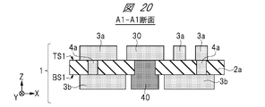
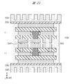
- FIG. 19 is a plan view showing the layer of the conductor 3b in the insulating substrate 1 in the fourth embodiment. 20 is a cross-sectional view taken along line A1-A1 shown in FIG. 19, and FIG. 21 is a cross-sectional view taken along line BB shown in FIG.
- a protruding conductor 40 is formed in the insulating plate 2a so as to be embedded inside the insulating plate 2a and protrude from the back surface BS1 of the insulating plate 2a.
- the protruding conductor 40 is electrically connected to the unconnected conductor 30, and is electrically insulated from the conductor 3b, the unconnected conductor 31, and the heat radiating conductor 5.
- a plurality of protruding conductors 40 as shown in FIG. 7 can be applied.
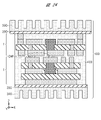
- FIG. 22 shows the power conversion device 100 using the insulating substrate 1 in the fourth embodiment.
- the heat radiating conductor 5 is connected to the heat sink 300 via the base plate 200. Further, also in the fourth embodiment, the insulating substrate 1, the plurality of semiconductor chip CHPs, and the bonding wire BW are covered with the protective member 400.
- the protective member 400 exists between the projecting conductor 40 and the conductor 3b which is the current path, and between the projecting conductor 40 and the base plate 200, these are electrically insulated.
- the protruding conductor 40 in the fourth embodiment protrudes toward the base plate 200 to the same extent as the conductor 3b, but the protruding conductor 40 may protrude to the extent that it does not come into contact with the base plate 200.
- the fourth embodiment As described above, according to the fourth embodiment, almost the same effect as that of the third embodiment can be obtained, and the heat dissipation can be further improved by the presence of the protruding conductor 40. Therefore, the reliability of the power converter 100 can be further improved.
- the insulating substrate 1 is mounted only on the back surface of the semiconductor chip CHP, but the insulating substrate 1 may also be mounted on the front surface of the semiconductor chip CHP.
- one insulating substrate 1 and the other insulating substrate 1 are arranged so that a plurality of conductors 3a face each other.
- the back surface of each of the plurality of semiconductor chip CHPs is placed on the plurality of conductors 3a of one insulating substrate 1, and the front surface of each of the plurality of semiconductor chip CHPs is placed on the plurality of conductors 3a of the other insulating substrate 1. It is installed in.
- at least one of the plurality of semiconductor chip CHPs is provided on the unconnected conductor 30 of one insulating substrate 1 and on the unconnected conductor 30 of the other insulating substrate 1.
- the heat-dissipating conductor 5 of one insulating substrate 1 and the heat-dissipating conductor 5 of the other insulating substrate 1 are each connected to the heat sink 300 via the base plate 200.
- the two sets of insulating substrates 1 and the plurality of semiconductor chip CHPs are covered with a protective member 400.
- the parasitic inductance Ls can be reduced. Further, since heat can be dissipated from both sides of the semiconductor chip CHP, the heat dissipation can be further improved. Therefore, the reliability of the power converter 100 can be improved.
- the two sets of insulating substrates 1 do not have to have the same structure as each other.
- the structure of the first embodiment may be applied to one insulating substrate 1 and the structure of the fourth embodiment may be applied to the other insulating substrate 1.
- the combination of the two sets of the insulating substrates 1 can be appropriately selected from the structures of the first to fourth embodiments.
- the base plate 200 and the heat sink 300 are not necessarily used. It does not have to be provided.
Landscapes
- Structure Of Printed Boards (AREA)
- Inverter Devices (AREA)
- Cooling Or The Like Of Semiconductors Or Solid State Devices (AREA)
Abstract
寄生インダクタンスを低く保つと共に、放熱性を高めることができる絶縁基板を提供する。また、そのような絶縁基板を用いることで、電力変換装置の信頼性を向上させる。絶縁基板1は、絶縁板2aと、絶縁板2bと、絶縁板2aの表面TS1に形成された複数の導電体3aと、絶縁板2aの裏面BS1と絶縁板2bの表面TS2との間に形成された導電体3bと、絶縁板2bの裏面BS2に形成された放熱導電体5と、絶縁板2aの内部に形成された複数の接続導電体4aとを備える。複数の導電体3aは、複数の接続導電体4aを介して導電体3bに電気的に接続されていない未接続導電体30を含む。絶縁板2aには、絶縁板2aの裏面BS1から突出するように、突出導電体40が形成されている。突出導電体40は、未接続導電体30に電気的に接続され、且つ、導電体3bおよび放熱導電体5と電気的に絶縁されている。
Description
本発明は、絶縁基板および電力変換装置に関し、特に、半導体チップを搭載するための絶縁基板、および、その絶縁基板を用いた電力変換装置に関する。
近年、SiCまたはGaNなどのようなワイドバンドギャップを有する化合物半導体基板を用いたパワー半導体チップが開発され、上記パワー半導体チップを搭載する電力変換装置が、市場に投入され始めた。SiCまたはGaNなどのパワー半導体チップは従来のSiパワー半導体チップよりも導通損失が小さいので、電力変換装置の冷却系の簡素化が図れる。
また、SiCまたはGaNなどのパワー半導体チップは高周波駆動が可能であるので、電力変換装置に含まれるインダクタまたはキャパシタのような受動部品の小型化が図れる。これらの効果によって、電力変換装置の全体のサイズを小さくすることが可能である。
高周波駆動を行う際、電力変換装置の寄生インダクタンスLsが課題となる。図1に示されるように、サージ電圧ΔVは、寄生インダクタンスLsと、単位時間当たりの電流量(di/dt)との積で表される。大きな寄生インダクタンスLsは、半導体チップのオフ時に大きなサージ電圧ΔVが印加される要因となり、ノイズの発生源にもなる。また、高周波駆動のためには、半導体チップのオフスピードも速くする必要があるが、サージ電圧ΔVおよびノイズは、上記オフスピードにも大きな影響を与える。
例えば、特許文献1には、絶縁板と、絶縁板の表面に形成された表面配線導体と、絶縁板の裏面に形成された裏面配線導体とを備えた絶縁基板が開示されている。表面配線導体上には、半導体チップが設置される。ここで、特許文献1には、表面配線導体に設けられたブリッジ端子を利用することで、近接逆方向通流の効果によって、寄生インダクタンスの低減を図る技術が開示されている。
本願発明者らは、化合物半導体基板向けの電力変換装置100として、図2に示される検討例1および図3に示される検討例2の構造を検討した。
図2に示されるように、検討例1の電力変換装置100では、絶縁板2a、絶縁板2aの表面に形成された複数の導電体3a、および、絶縁板2aの裏面に形成された放熱導電体5を備えた絶縁基板1が用いられる。
複数の導電体3a上には、複数の半導体チップCHPが設置され、複数の導電体3aおよび複数の半導体チップCHPは、ボンディングワイヤBWによって適宜電気的に接続されている。また、放熱導電体5は、ベースプレート200を介してヒートシンク300に接続されている。
一方で、図3に示されるように、検討例2の電力変換装置100は、絶縁板2aと放熱導電体5との間に、導電体3bおよび絶縁板2bを更に備え、多層絶縁基板構造を成している。このため、検討例2では、絶縁板と、電流が流れる導電体とが数層に渡って積層されているので、検討例1と比較して、相互インダクタンスによって寄生インダクタンスLsを低減することができる。
しかしながら、検討例2では、多層絶縁基板構造を成すことで、熱源である半導体チップCHPから冷却系(ヒートシンク300)までの距離が遠くなってしまうので、検討例1と比較して、熱抵抗が大きくなることで半導体チップCHPの温度が上昇し易くなってしまう。その結果、最大温度と最低温度との温度差が大きくなることで、半導体チップCHPから導電体3aが剥離し易くなる。また、放熱導電体5とベースプレート200との間、および、ベースプレート200とヒートシンク300との間でも同様に、剥離が起き易くなる。そして、半導体チップCHPだけでなく、電力変換装置100の全体としての温度も上昇し易くなるので、電力変換装置100の信頼性が低下し、製品寿命が短くなってしまうという問題がある。
従って、寄生インダクタンスLsを低く保つと共に、放熱性を高めることができる絶縁基板1の開発が望まれ、それによって電力変換装置100の信頼性を向上させることが望まれる。その他の課題および新規な特徴は、本明細書の記述および添付図面から明らかになる。
本願において開示される実施の形態のうち、代表的なものの概要を簡単に説明すれば、次のとおりである。
一実施の形態である絶縁基板は、表面および裏面を有する第1絶縁板と、前記第1絶縁板の裏面側に形成され、且つ、表面および裏面を有する第2絶縁板と、前記第1絶縁板の表面に形成された複数の第1導電体と、前記第1絶縁板の裏面と前記第2絶縁板の表面との間に形成された第2導電体と、前記第2絶縁板の裏面に形成され、且つ、前記第2導電体と電気的に絶縁された放熱導電体と、前記複数の第1導電体の一部および前記第2導電体を電気的に接続させるように、前記第1絶縁板の内部に形成された複数の第1接続導電体と、を備える。ここで、前記複数の第1導電体は、前記複数の第1接続導電体を介して前記第2導電体に電気的に接続されていない第1未接続導電体を含み、前記第1絶縁板には、前記第1絶縁板の内部に埋め込まれ、且つ、前記第1絶縁板の裏面から突出するように、突出導電体が形成され、前記突出導電体は、前記第1未接続導電体に電気的に接続され、且つ、前記第2導電体および前記放熱導電体と電気的に絶縁されている。
また、一実施の形態である絶縁基板は、表面および裏面を有する第1絶縁板と、前記第1絶縁板の表面に形成された複数の第1導電体と、前記第1絶縁板の裏面に形成された複数の第2導電体と、前記複数の第1導電体の一部および前記複数の第2導電体の一部を電気的に接続させるように、前記第1絶縁板の内部に形成された複数の第1接続導電体と、を備える。ここで、前記複数の第2導電体は、他の前記第2導電体と電気的に絶縁された第2未接続導電体を含み、前記第2未接続導電体には、前記第1絶縁板の裏面側において前記他の前記第2導電体よりも突出するように、放熱導電体が接続されている。
一実施の形態によれば、寄生インダクタンスを低く保つと共に、放熱性を高めることができる絶縁基板を提供できる。また、そのような絶縁基板を用いることで、電力変換装置の信頼性を向上させることができる。
以下、本発明の実施の形態を図面に基づいて詳細に説明する。なお、実施の形態を説明するための全図において、同一の機能を有する部材には同一の符号を付し、その繰り返しの説明は省略する。また、以下の実施の形態では、特に必要なときを除き、同一または同様な部分の説明を原則として繰り返さない。
また、本願で説明されるX方向、Y方向およびZ方向は、互いに交差し、互いに直交している。本願では、Z方向をある構造体の縦方向、上下方向、高さ方向または厚さ方向として説明する。また、本願で用いられる「平面視」という表現は、X方向およびY方向によって構成される面を、Z方向から見ることを意味する。
(実施の形態1)
<絶縁基板1の構成>
以下に図4~図7を用いて、実施の形態1における絶縁基板1について説明する。図4は、絶縁基板1を示す斜視図であり、図5は、図4に示されるA1-A1線に沿った断面図である。図6および図7は、絶縁基板1のうち導電体3bの層を示す平面図である。
<絶縁基板1の構成>
以下に図4~図7を用いて、実施の形態1における絶縁基板1について説明する。図4は、絶縁基板1を示す斜視図であり、図5は、図4に示されるA1-A1線に沿った断面図である。図6および図7は、絶縁基板1のうち導電体3bの層を示す平面図である。
絶縁基板1は、絶縁板と、電流が流れる導電体とが数層に渡って積層された多層絶縁基板構造を成している。絶縁基板1は、絶縁板2aと、絶縁板2bと、複数の導電体3aと、導電体3bと、複数の接続導電体4aと、放熱導電体5とを備えている。
絶縁板2aは、表面TS1および裏面BS1を有する。図4に示されるように、絶縁板2aの表面TS1には、複数の導電体3aが形成されている。また、複数の導電体3aは、未接続導電体30を含んでいる。
図5に示されるように、絶縁板2bは、絶縁板2aの裏面BS1側に形成され、表面TS2および裏面BS2を有する。絶縁板2aの裏面BS1と絶縁板2bの表面TS2との間には、導電体3bが形成されている。絶縁板2aの内部には、複数の導電体3aの一部および導電体3bを電気的に接続させるように、複数の接続導電体4aが形成されている。また、絶縁板2bの裏面BS2には、導電体3bと電気的に絶縁された放熱導電体5が形成されている。
後述するように、複数の導電体3aには、複数の半導体チップ、コンデンサおよびインダクタなどの様々な電子デバイスが設置されるが、複数の導電体3a、複数の接続導電体4aおよび導電体3bが電気的に接続されていることで、上記電子デバイス間の電気的な導通が成され、電流経路が構築される。なお、ここでは、導電体3bが1つである場合を例示しているが、複数の導電体3bが設けられていてもよい。その場合、複数の導電体3bによって、より複雑な回路を構築することができる。
このような実施の形態1における絶縁基板1では、電流経路が多層化しているので、相互インダクタンスによって寄生インダクタンスLsを低減することができる。
上述のように、複数の導電体3a上に複数の半導体チップが設置された場合、絶縁基板1が多層絶縁基板構造を成しているので、複数の半導体チップと放熱導電体5との間の距離が長くなり、放熱性が低下し易くなるという問題がある。
ここで、複数の導電体3aには、複数の接続導電体4aを介して導電体3bに電気的に接続されていない未接続導電体30が含まれている。未接続導電体30の下方に、電流経路とは電気的に絶縁された放熱経路を設けることで、放熱性を向上させることができる。
図5に示されるように、絶縁板2aには、絶縁板2aの内部に埋め込まれ、且つ、絶縁板2aの裏面BS1から突出するように、突出導電体40が形成されている。突出導電体40は、未接続導電体30に電気的に接続され、絶縁板2bによって放熱導電体5と電気的に絶縁されている。
また、図5および図6に示されるように、突出導電体40は、平面視において突出導電体40を囲む絶縁層41によって、導電体3bと電気的に絶縁されている。このような突出導電体40を、導電体3bなどで構成される電気経路とは独立した放熱経路として利用することで、寄生インダクタンスLsを低く保つと共に、放熱性を高めることができる。
また、突出導電体40は、図6のように1つだけでなく、図7のように複数個設けられていてもよい。図7では、絶縁板2aには、複数の突出導電体40が形成されている。複数の突出導電体40は、それぞれ、未接続導電体30に電気的に接続され、絶縁層41によって導電体3bと電気的に絶縁され、絶縁板2bによって放熱導電体5と電気的に絶縁されている。
図7の場合、1つ当たりの突出導電体40の平面積が図6よりも小さくなるが、複数の突出導電体40の合計平面積が図6と同程度になるように設計すれば、図7でも図6と同程度の放熱性を確保できる。
なお、未接続導電体30を含む複数の導電体3aと、導電体3bと、放熱導電体5と、複数の接続導電体4aと、突出導電体40とは、例えば、銅(Cu)またはアルミニウム(Al)を含む金属材料からなる。また、絶縁板2aと、絶縁板2bとは、例えば、セラミックまたは樹脂材料からなる。
<電力変換装置100の構成>
以下に図8~図10を用いて、実施の形態1における電力変換装置100について説明する。図8は、電力変換装置100を示す斜視図であり、図9および図10は、図8に示されるA2-A2線に沿った断面図である。なお、A2-A2線は、図4および図6に示されるA1-A1線と同一直線上に位置する。
以下に図8~図10を用いて、実施の形態1における電力変換装置100について説明する。図8は、電力変換装置100を示す斜視図であり、図9および図10は、図8に示されるA2-A2線に沿った断面図である。なお、A2-A2線は、図4および図6に示されるA1-A1線と同一直線上に位置する。
電力変換装置100は、絶縁基板1と、複数の半導体チップCHPと、ボンディングワイヤBWと、ベースプレート200と、ヒートシンク300とを備える。
図8および図9に示されるように、ヒートシンク300は、ベースプレート200を介して放熱導電体5に接続されている。ここで、放熱導電体5およびベースプレート200は、TIM(Thermal interface material)を介して接続されている。また、ベースプレート200およびヒートシンク300も、TIMを介して接続されている。TIMは、例えば、はんだまたは焼結材といった材料である。複数の半導体チップCHPは、それぞれ表面および裏面を有し、複数の半導体チップCHPの各々の裏面は、TIMによって複数の導電体3a上に設置されている。また、複数の半導体チップCHPのうち少なくとも1つは、未接続導電体30上に設けられている。複数の半導体チップCHPおよび複数の導電体3aは、ボンディングワイヤBWによって適宜電気的に接続されている。
なお、特に図示はしないが、複数の導電体3a上には、複数の半導体チップCHPの他に、コンデンサおよびインダクタなどの他の電子デバイスが設置されている場合もある。
また、図10に示されるように、電力変換装置100のうち、絶縁基板1、複数の半導体チップCHPおよびボンディングワイヤBWは、保護部材400によって覆われていてもよい。これにより、絶縁基板1、半導体チップCHPおよびボンディングワイヤBWが、外部環境との間で放電することを防止できる。保護部材400は、絶縁材料からなり、例えば絶縁ゲルまたはモールド樹脂からなる。
なお、半導体チップCHPは、例えば、炭化珪素(SiC)、窒化ガリウム(GaN)または酸化ガリウム(Ga2O3)のような化合物半導体基板と、上記化合物半導体基板に形成されたMOSFETのようなトランジスタとを含む。
ボンディングワイヤBWは、例えば、金(Au)、銅(Cu)またはアルミニウム(Al)を含む金属材料からなる。また、ボンディングワイヤBWに代えて、リボンまたはバスバーなどによって複数の半導体チップCHPおよび複数の導電体3aを電気的に接続させてもよい。
ベースプレート200は、例えば、銅(Cu)、アルミニウム合金の中にSiCセラミックス粒子を含有させた複合材料(AlSiC)またはマグネシウムの中にSiCセラミックス粒子を含有させた複合材料(MgSiC)からなる。ヒートシンク300は、例えば、銅(Cu)、鉄(Fe)またはアルミニウムを含む金属材料からなる。
図11および図12は、実施の形態1の効果を示すグラフであり、本願発明者らが計測したシミュレーション結果である。なお、図11および図12には、後述の実施の形態3の効果も示されている。また、図11および図12の横軸の「Heat area」は、実施の形態1では、平面視における突出導電体40の面積を示している。
図11および図12に示されるように、実施の形態1の電力変換装置100では、検討例2(図3)と比較して温度の上昇を抑制できており、寄生インダクタンスLsを検討例2(図3)と同程度に保つことができる。すなわち、実施の形態1によれば、寄生インダクタンスLsを低く保つと共に、放熱性を高めることができる絶縁基板1を提供でき、そのような絶縁基板1を用いることで、電力変換装置100の信頼性を向上させることができる。
(実施の形態2)
以下に図13および図14を用いて、実施の形態2における絶縁基板1および電力変換装置100について説明する。なお、以下の説明では、実施の形態1との相違点について主に説明し、実施の形態1と重複する点についての説明を省略する。
以下に図13および図14を用いて、実施の形態2における絶縁基板1および電力変換装置100について説明する。なお、以下の説明では、実施の形態1との相違点について主に説明し、実施の形態1と重複する点についての説明を省略する。
実施の形態2における絶縁基板1は、実施の形態1と比較して、絶縁板2bと放熱導電体5との間に更に多くの絶縁板および導電体が積層された多層絶縁基板構造を成している。
図13に示されるように、絶縁板2bと放熱導電体5との間には、表面TS3および裏面BS3を有する絶縁板2cが形成されている。導電体3cは、絶縁板2bの裏面BS2と絶縁板2cの表面TS3との間に形成されている。絶縁板2bの内部には、導電体3bと導電体3cとを電気的に接続させるように、複数の接続導電体4bが形成されている。そして、突出導電体40は、絶縁板2bを貫通し、絶縁板2bの裏面から突出し、且つ、導電体3cおよび接続導電体4bと電気的に絶縁されている。
このように、実施の形態2では、絶縁板2bから放熱導電体5に渡って、絶縁板2c、導電体3c、複数の接続導電体4bおよび突出導電体40を含む構造体が、1回以上繰り返し形成されている。例えば、上記構造体を2回繰り返した場合、図13に示される導電体3dおよび接続導電体4cなどが形成される。
図14は、実施の形態2における絶縁基板1を用いた電力変換装置100を示している。実施の形態2でも、更に多層化された絶縁基板1、複数の半導体チップCHPおよびボンディングワイヤBWは、保護部材400によって覆われていてもよい。
複数の導電体3a上には、複数の半導体チップCHP、コンデンサおよびインダクタなどの様々な電子デバイスが設置されるが、絶縁基板1が更に多層化されていることで、これらの電子デバイスの結線経路を自由に設計し易くなり、回路設計の自由度を高めることができる。また、寄生インダクタLsを低減させるための電流経路についても、自由に設計し易くなる。
なお、このように絶縁基板1を更に多層化した場合でも、突出導電体40が各絶縁板を貫通しているので、放熱経路を確保できる。そのため、放熱性の低下を抑制することができる。従って、絶縁基板1を用いた電力変換装置100の信頼性を向上させることができる。
(実施の形態3)
以下に図15~図18を用いて、実施の形態3における絶縁基板1および電力変換装置100について説明する。なお、以下の説明では、実施の形態1との相違点について主に説明し、実施の形態1と重複する点についての説明を省略する。
以下に図15~図18を用いて、実施の形態3における絶縁基板1および電力変換装置100について説明する。なお、以下の説明では、実施の形態1との相違点について主に説明し、実施の形態1と重複する点についての説明を省略する。
実施の形態1では、絶縁基板1を多層絶縁基板構造とした場合に、未接続導電体30に突出導電体40を接続させることで、放熱性の向上を図っていた。実施の形態3では、絶縁基板1を単層絶縁基板構造とした場合に、他の手段によって放熱性の向上を図っている。
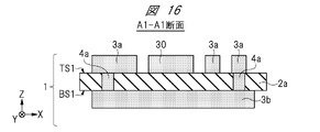
図15は、実施の形態3における絶縁基板1のうち導電体3bの層を示す平面図である。図16は、図15に示されるA1-A1線に沿った断面図であり、図17は、図15に示されるB-B線に沿った断面図である。
図16に示されるように、実施の形態3における複数の導電体3a、未接続導電体30、絶縁板2aおよび接続導電体4aについては、実施の形態1と同様である。しかし、実施の形態3では、絶縁板2bが形成されておらず、未接続導電体30に接続させるための突出導電体40も形成されていない。
また、図15および図17に示されるように、実施の形態3では、複数の導電体3bが形成され、複数の導電体3bには、他の導電体3bと電気的に絶縁された未接続導電体31が含まれる。未接続導電体31は、他の導電体3bおよび接続導電体4aと電気的に絶縁されている。なお、ここでは、絶縁基板1の4隅に、それぞれ未接続導電体31が設けられているが、未接続導電体31の数および位置は、適宜変更可能である。
複数の未接続導電体31には、絶縁板2aの裏面BS1側において他の導電体3bよりも突出するように、それぞれ放熱導電体5が接続されている。すなわち、未接続導電体31以外の導電体3bには、放熱導電体5が接続されていない。言い換えれば、未接続導電体31および放熱導電体5の合計厚さは、未接続導電体31以外の導電体3bの厚さよりも厚い。
このように、実施の形態3では、未接続導電体31以外の導電体3bが電流経路となり、未接続導電体31および放熱導電体5が、電流経路から絶縁された放熱経路を構成している。
なお、未接続導電体31は複数の導電体3aと電気的に絶縁されているので、未接続導電体31の上方に、複数の導電体3aを自由に配置させることができる。複数の導電体3aの配置面積を多くすることで、絶縁板2aの表面TS1側からの放熱性を高めることができる。また、複数の導電体3aのうち一部が電流経路に含まれていない場合、一部の導電体3aの下部に接続導電体4aを設け、その接続導電体4aを介して、一部の導電体3aと未接続導電体31とを接続させてもよい。このような方法によっても放熱性を高めることができる。
図18は、実施の形態3における絶縁基板1を用いた電力変換装置100を示している。放熱導電体5は、ベースプレート200を介してヒートシンク300に接続される。また、実施の形態3でも、絶縁基板1、複数の半導体チップCHPおよびボンディングワイヤBWは、保護部材400によって覆われている。
ここで、電流経路となる導電体3bと未接続導電体31との間、および、電流経路となる導電体3bとベースプレート200との間には、保護部材400が存在しているので、これらは電気的に絶縁されている。
図11および図12には、実施の形態3の効果が示されている。なお、図11および図12の横軸の「Heat area」は、実施の形態3では、平面視における放熱導電体5の面積(ここでは4つの放熱導電体5の合計面積)を示している。
図11および図12に示されるように、実施の形態3の電力変換装置100では、検討例2(図3)と比較して温度の上昇を抑制できている。一方で、実施の形態3の絶縁基板1は基本的に単層絶縁基板構造であるので、実施の形態3では、検討例2(図3)と比較して、寄生インダクタンスLsが高くなっているが、実施の形態3は、単層絶縁基板構造である検討例1(図1)と比較すると、同程度の寄生インダクタンスLsとなる。
すなわち、実施の形態3においても、寄生インダクタンスLsを低く保つと共に、放熱性を高めることができる絶縁基板1を提供でき、そのような絶縁基板1を用いることで、電力変換装置100の信頼性を向上させることができる。
(実施の形態4)
以下に図19~図22を用いて、実施の形態4における絶縁基板1および電力変換装置100について説明する。なお、以下の説明では、実施の形態3との相違点について主に説明し、実施の形態3と重複する点についての説明を省略する。
以下に図19~図22を用いて、実施の形態4における絶縁基板1および電力変換装置100について説明する。なお、以下の説明では、実施の形態3との相違点について主に説明し、実施の形態3と重複する点についての説明を省略する。
実施の形態4では、実施の形態3の絶縁基板1を基にして、実施の形態1で説明した突出導電体40が適用されている。
図19は、実施の形態4における絶縁基板1のうち導電体3bの層を示す平面図である。図20は、図19に示されるA1-A1線に沿った断面図であり、図21は、図19に示されるB-B線に沿った断面図である。
図19~図21に示されるように、絶縁板2aには、絶縁板2aの内部に埋め込まれ、且つ、絶縁板2aの裏面BS1から突出するように、突出導電体40が形成されている。突出導電体40は、未接続導電体30に電気的に接続され、導電体3b、未接続導電体31および放熱導電体5と電気的に絶縁されている。なお、実施の形態4においても、図7のような複数の突出導電体40を適用できる。
図22は、実施の形態4における絶縁基板1を用いた電力変換装置100を示している。放熱導電体5は、ベースプレート200を介してヒートシンク300に接続される。また、実施の形態4でも、絶縁基板1、複数の半導体チップCHPおよびボンディングワイヤBWは、保護部材400によって覆われている。
ここで、突出導電体40と電流経路となる導電体3bとの間、および、突出導電体40とベースプレート200との間には、保護部材400が存在しているので、これらは電気的に絶縁されている。なお、実施の形態4における突出導電体40は、導電体3bと同程度にベースプレート200側へ突出しているが、突出導電体40は、ベースプレート200に接触しない程度に突出していればよい。
このように、実施の形態4によれば、実施の形態3とほぼ同様の効果を得られると共に、突出導電体40の存在によって放熱性を更に向上させることができる。従って、電力変換装置100の信頼性を更に向上させることができる。
(変形例)
以下に図23および図24を用いて、実施の形態1~4の変形例における電力変換装置100について説明する。
以下に図23および図24を用いて、実施の形態1~4の変形例における電力変換装置100について説明する。
実施の形態1~4における電力変換装置100は、半導体チップCHPの裏面のみに絶縁基板1が実装されていたが、半導体チップCHPの表面にも絶縁基板1が実装されていてもよい。
図23に示されるように、一方の絶縁基板1と他方の絶縁基板1とは、互いの複数の導電体3aが向き合うように配置されている。複数の半導体チップCHPの各々の裏面は、一方の絶縁基板1の複数の導電体3a上に設置され、複数の半導体チップCHPの各々の表面は、他方の絶縁基板1の複数の導電体3a上に設置されている。ここで、複数の半導体チップCHPのうち少なくとも1つは、一方の絶縁基板1の未接続導電体30上、および、他方の絶縁基板1の未接続導電体30上に設けられる。
一方の絶縁基板1の放熱導電体5、および、他方の絶縁基板1の放熱導電体5は、それぞれ、ベースプレート200を介してヒートシンク300に接続されている。2組の絶縁基板1および複数の半導体チップCHPは、保護部材400によって覆われている。
このように、2組の絶縁基板1によって半導体チップCHPの両面を挟み込む構造においても、寄生インダクタンスLsの低減を図れる。また、半導体チップCHPの両面からの放熱が可能となるので、放熱性を更に向上させることができる。従って、電力変換装置100の信頼性を向上させることができる。
また、2組の絶縁基板1は、互いに同じ構造でなくてもよい。例えば、図24に示されるように、一方の絶縁基板1に実施の形態1の構造を適用し、他方の絶縁基板1に実施の形態4の構造を適用してもよい。このように、2組の絶縁基板1の組み合わせは、実施の形態1~4の構造から適宜選択できる。
また、2組の絶縁基板1を用いた電力変換装置100では、半導体チップCHPの両面からの放熱が可能となるので、その放熱量が十分である場合には、ベースプレート200およびヒートシンク300は、必ずしも設けられていなくてもよい。
以上、本発明を上記実施の形態に基づいて具体的に説明したが、本発明は、上記実施の形態に限定されるものではなく、その要旨を逸脱しない範囲で種々変更可能である。
1 絶縁基板
2a~2c 絶縁板
3a~3d 導電体
4a~4c 接続導電体
5 放熱導電体
30、31 未接続導電体
40 突出導電体
41 絶縁層
100 電力変換装置
200 ベースプレート
300 ヒートシンク
400 保護部材
BS1~BS3 裏面
BW ボンディングワイヤ
CHP 半導体チップ
TS1~TS3 表面
2a~2c 絶縁板
3a~3d 導電体
4a~4c 接続導電体
5 放熱導電体
30、31 未接続導電体
40 突出導電体
41 絶縁層
100 電力変換装置
200 ベースプレート
300 ヒートシンク
400 保護部材
BS1~BS3 裏面
BW ボンディングワイヤ
CHP 半導体チップ
TS1~TS3 表面
Claims (15)
- 表面および裏面を有する第1絶縁板と、
前記第1絶縁板の裏面側に形成され、且つ、表面および裏面を有する第2絶縁板と、
前記第1絶縁板の表面に形成された複数の第1導電体と、
前記第1絶縁板の裏面と前記第2絶縁板の表面との間に形成された第2導電体と、
前記第2絶縁板の裏面に形成され、且つ、前記第2導電体と電気的に絶縁された放熱導電体と、
前記複数の第1導電体の一部および前記第2導電体を電気的に接続させるように、前記第1絶縁板の内部に形成された複数の第1接続導電体と、
を備え、
前記複数の第1導電体は、前記複数の第1接続導電体を介して前記第2導電体に電気的に接続されていない第1未接続導電体を含み、
前記第1絶縁板には、前記第1絶縁板の内部に埋め込まれ、且つ、前記第1絶縁板の裏面から突出するように、突出導電体が形成され、
前記突出導電体は、前記第1未接続導電体に電気的に接続され、且つ、前記第2導電体および前記放熱導電体と電気的に絶縁されている、絶縁基板。 - 請求項1に記載の絶縁基板において、
前記第1絶縁板には、複数の前記突出導電体が形成され、
前記複数の前記突出導電体は、それぞれ、前記第1未接続導電体に電気的に接続され、且つ、前記第2導電体および前記放熱導電体と電気的に絶縁されている、絶縁基板。 - 請求項1に記載の絶縁基板において、
前記第2絶縁板と前記放熱導電体との間に形成され、且つ、表面および裏面を有する第3絶縁板と、
前記第2絶縁板の裏面と前記第3絶縁板の表面との間に形成された第3導電体と、
前記第2導電体と前記第3導電体とを電気的に接続させるように、前記第2絶縁板の内部に形成された複数の第2接続導電体と、
を更に備え、
前記突出導電体は、前記第2絶縁板を貫通し、前記第2絶縁板の裏面から突出し、且つ、前記第3導電体および前記第2接続導電体と電気的に絶縁され、
前記第2絶縁板から前記放熱導電体に渡って、前記第3絶縁板、前記第3導電体、前記複数の第2接続導電体および前記突出導電体を含む構造体が、1回以上繰り返し形成されている、絶縁基板。 - 請求項1に記載の絶縁基板を用いた電力変換装置であって、
表面および裏面を有する複数の半導体チップと、
前記放熱導電体にベースプレートを介して接続されたヒートシンクと、
を備え、
前記複数の半導体チップの各々の裏面は、前記複数の第1導電体上に設置され、
前記複数の半導体チップのうち少なくとも1つは、前記第1未接続導電体上に設けられている、電力変換装置。 - 請求項1に記載の絶縁基板を用いた電力変換装置であって、
表面および裏面を有する複数の半導体チップと、
2組の前記絶縁基板と、
を備え、
一方の前記絶縁基板と他方の前記絶縁基板とは、互いの前記複数の第1導電体が向き合うように配置され、
前記複数の半導体チップの各々の裏面は、前記一方の前記絶縁基板の前記複数の第1導電体上に設置され、
前記複数の半導体チップの各々の表面は、前記他方の前記絶縁基板の前記複数の第1導電体上に設置され、
前記複数の半導体チップのうち少なくとも1つは、前記一方の前記絶縁基板の前記第1未接続導電体上、および、前記他方の前記絶縁基板の前記第1未接続導電体上に設けられている、電力変換装置。 - 請求項5に記載の電力変換装置において、
前記一方の前記絶縁基板の前記放熱導電体、および、前記他方の前記絶縁基板の前記放熱導電体には、それぞれ、ベースプレートを介してヒートシンクが接続されている、電力変換装置。 - 請求項4に記載の電力変換装置において、
前記複数の半導体チップは、化合物半導体基板と、前記化合物半導体基板に形成されたトランジスタとを含む、電力変換装置。 - 表面および裏面を有する第1絶縁板と、
前記第1絶縁板の表面に形成された複数の第1導電体と、
前記第1絶縁板の裏面に形成された複数の第2導電体と、
前記複数の第1導電体の一部および前記複数の第2導電体の一部を電気的に接続させるように、前記第1絶縁板の内部に形成された複数の第1接続導電体と、
を備え、
前記複数の第2導電体は、他の前記第2導電体と電気的に絶縁された第2未接続導電体を含み、
前記第2未接続導電体には、前記第1絶縁板の裏面側において前記他の前記第2導電体よりも突出するように、放熱導電体が接続されている、絶縁基板。 - 請求項8に記載の絶縁基板において、
前記複数の第2導電体は、複数の前記第2未接続導電体を含み、
前記複数の前記第2未接続導電体の各々には、前記放熱導電体が接続されている、絶縁基板。 - 請求項8に記載の絶縁基板において、
前記複数の第1導電体は、前記複数の第1接続導電体を介して前記複数の第2導電体に電気的に接続されていない第1未接続導電体を含み、
前記第1絶縁板には、前記第1絶縁板の内部に埋め込まれ、且つ、前記第1絶縁板の裏面から突出するように、突出導電体が形成され、
前記突出導電体は、前記第1未接続導電体に電気的に接続され、且つ、前記複数の第2導電体、前記第2未接続導電体および前記放熱導電体と電気的に絶縁されている、絶縁基板。 - 請求項10に記載の絶縁基板において、
前記第1絶縁板には、複数の前記突出導電体が形成され、
前記複数の前記突出導電体は、それぞれ、前記第1未接続導電体に電気的に接続され、且つ、前記複数の第2導電体および前記放熱導電体と電気的に絶縁されている、絶縁基板。 - 請求項8に記載の絶縁基板を用いた電力変換装置であって、
表面および裏面を有する複数の半導体チップと、
前記放熱導電体にベースプレートを介して接続されたヒートシンクと、
を備え、
前記複数の半導体チップの各々の裏面は、前記複数の第1導電体上に設置されている、電力変換装置。 - 請求項8に記載の絶縁基板を用いた電力変換装置であって、
表面および裏面を有する複数の半導体チップと、
2組の前記絶縁基板と、
を備え、
一方の前記絶縁基板と他方の前記絶縁基板とは、互いの前記複数の第1導電体が向き合うように配置され、
前記複数の半導体チップの各々の裏面は、前記一方の前記絶縁基板の前記複数の第1導電体上に設置され、
前記複数の半導体チップの各々の表面は、前記他方の前記絶縁基板の前記複数の第1導電体上に設置されている、電力変換装置。 - 請求項13に記載の電力変換装置において、
前記一方の前記絶縁基板の前記放熱導電体、および、前記他方の前記絶縁基板の前記放熱導電体には、それぞれ、ベースプレートを介してヒートシンクが接続されている、電力変換装置。 - 請求項12に記載の電力変換装置において、
前記複数の半導体チップは、化合物半導体基板と、前記化合物半導体基板に形成されたトランジスタとを含む、電力変換装置。
Priority Applications (1)
| Application Number | Priority Date | Filing Date | Title |
|---|---|---|---|
| EP21900266.4A EP4258337B1 (en) | 2020-12-03 | 2021-09-01 | Insulated board and power converter |
Applications Claiming Priority (2)
| Application Number | Priority Date | Filing Date | Title |
|---|---|---|---|
| JP2020200810A JP7535444B2 (ja) | 2020-12-03 | 2020-12-03 | 絶縁基板および電力変換装置 |
| JP2020-200810 | 2020-12-03 |
Publications (1)
| Publication Number | Publication Date |
|---|---|
| WO2022118510A1 true WO2022118510A1 (ja) | 2022-06-09 |
Family
ID=81852691
Family Applications (1)
| Application Number | Title | Priority Date | Filing Date |
|---|---|---|---|
| PCT/JP2021/032188 Ceased WO2022118510A1 (ja) | 2020-12-03 | 2021-09-01 | 絶縁基板および電力変換装置 |
Country Status (3)
| Country | Link |
|---|---|
| EP (1) | EP4258337B1 (ja) |
| JP (1) | JP7535444B2 (ja) |
| WO (1) | WO2022118510A1 (ja) |
Cited By (1)
| Publication number | Priority date | Publication date | Assignee | Title |
|---|---|---|---|---|
| CN115580225A (zh) * | 2022-11-04 | 2023-01-06 | 大庆华研环保应用技术研发中心有限公司 | 一种聚光光伏电池基板散热结构 |
Citations (5)
| Publication number | Priority date | Publication date | Assignee | Title |
|---|---|---|---|---|
| JP2013008940A (ja) * | 2011-05-26 | 2013-01-10 | Napura:Kk | 電子機器用基板及び電子機器 |
| WO2014175062A1 (ja) * | 2013-04-24 | 2014-10-30 | 富士電機株式会社 | パワー半導体モジュールおよびその製造方法、電力変換器 |
| WO2015049944A1 (ja) * | 2013-10-03 | 2015-04-09 | 富士電機株式会社 | 半導体モジュール |
| JP2015185630A (ja) * | 2014-03-24 | 2015-10-22 | 日産自動車株式会社 | ハーフブリッジパワー半導体モジュール及びその製造方法 |
| JP2019046899A (ja) * | 2017-08-31 | 2019-03-22 | ルネサスエレクトロニクス株式会社 | 電子装置 |
Family Cites Families (2)
| Publication number | Priority date | Publication date | Assignee | Title |
|---|---|---|---|---|
| WO2016002385A1 (ja) * | 2014-07-03 | 2016-01-07 | 日産自動車株式会社 | ハーフブリッジパワー半導体モジュール及びその製造方法 |
| FR3084960B1 (fr) * | 2018-08-07 | 2020-10-23 | Safran Electrical & Power | Circuit electrique de puissance pour convertisseur de puissance electrique |
-
2020
- 2020-12-03 JP JP2020200810A patent/JP7535444B2/ja active Active
-
2021
- 2021-09-01 EP EP21900266.4A patent/EP4258337B1/en active Active
- 2021-09-01 WO PCT/JP2021/032188 patent/WO2022118510A1/ja not_active Ceased
Patent Citations (5)
| Publication number | Priority date | Publication date | Assignee | Title |
|---|---|---|---|---|
| JP2013008940A (ja) * | 2011-05-26 | 2013-01-10 | Napura:Kk | 電子機器用基板及び電子機器 |
| WO2014175062A1 (ja) * | 2013-04-24 | 2014-10-30 | 富士電機株式会社 | パワー半導体モジュールおよびその製造方法、電力変換器 |
| WO2015049944A1 (ja) * | 2013-10-03 | 2015-04-09 | 富士電機株式会社 | 半導体モジュール |
| JP2015185630A (ja) * | 2014-03-24 | 2015-10-22 | 日産自動車株式会社 | ハーフブリッジパワー半導体モジュール及びその製造方法 |
| JP2019046899A (ja) * | 2017-08-31 | 2019-03-22 | ルネサスエレクトロニクス株式会社 | 電子装置 |
Non-Patent Citations (1)
| Title |
|---|
| See also references of EP4258337A4 * |
Cited By (1)
| Publication number | Priority date | Publication date | Assignee | Title |
|---|---|---|---|---|
| CN115580225A (zh) * | 2022-11-04 | 2023-01-06 | 大庆华研环保应用技术研发中心有限公司 | 一种聚光光伏电池基板散热结构 |
Also Published As
| Publication number | Publication date |
|---|---|
| JP7535444B2 (ja) | 2024-08-16 |
| EP4258337A1 (en) | 2023-10-11 |
| EP4258337A4 (en) | 2024-10-09 |
| JP2022088783A (ja) | 2022-06-15 |
| EP4258337B1 (en) | 2025-12-24 |
Similar Documents
| Publication | Publication Date | Title |
|---|---|---|
| US10638633B2 (en) | Power module, power converter and manufacturing method of power module | |
| US7786486B2 (en) | Double-sided package for power module | |
| US10892205B2 (en) | Package structure and power module using same | |
| US20130328200A1 (en) | Direct bonded copper substrate and power semiconductor module | |
| JP5672305B2 (ja) | 半導体装置 | |
| CN102593081A (zh) | 包括散热器的半导体器件 | |
| TW202406444A (zh) | 基於頂側冷卻表面安裝離散裝置之雙面散熱型電源供應器 | |
| JP2022095471A (ja) | パワー部品内蔵基板及び部品内蔵基板形成方法 | |
| KR101946467B1 (ko) | 반도체 장치의 방열구조 | |
| JP2007012831A (ja) | パワー半導体装置 | |
| JP2010045399A (ja) | パワー半導体装置 | |
| JP4146888B2 (ja) | 半導体モジュールと半導体モジュールの製造方法 | |
| WO2012081434A1 (ja) | 半導体装置 | |
| US11081412B2 (en) | Semiconductor device | |
| JP2019134018A (ja) | 半導体装置 | |
| US20140001611A1 (en) | Semiconductor package | |
| WO2022118510A1 (ja) | 絶縁基板および電力変換装置 | |
| JP7306294B2 (ja) | 半導体モジュール | |
| JP7512706B2 (ja) | 半導体装置 | |
| JP2020141023A (ja) | 半導体装置 | |
| CN111834307B (zh) | 半导体模块 | |
| US20250380362A1 (en) | Circuit assembly with two circuit carriers and a semiconductor component | |
| JP2011192762A (ja) | パワーモジュール | |
| JP7778271B2 (ja) | 半導体装置及びその製造方法 | |
| CN116705709A (zh) | 用于包括底部冷却式半导体功率开关器件的功率级组件的基板 |
Legal Events
| Date | Code | Title | Description |
|---|---|---|---|
| 121 | Ep: the epo has been informed by wipo that ep was designated in this application |
Ref document number: 21900266 Country of ref document: EP Kind code of ref document: A1 |
|
| NENP | Non-entry into the national phase |
Ref country code: DE |
|
| ENP | Entry into the national phase |
Ref document number: 2021900266 Country of ref document: EP Effective date: 20230703 |
|
| WWG | Wipo information: grant in national office |
Ref document number: 2021900266 Country of ref document: EP |