WO2022123697A1 - 電力変換装置 - Google Patents
電力変換装置 Download PDFInfo
- Publication number
- WO2022123697A1 WO2022123697A1 PCT/JP2020/045900 JP2020045900W WO2022123697A1 WO 2022123697 A1 WO2022123697 A1 WO 2022123697A1 JP 2020045900 W JP2020045900 W JP 2020045900W WO 2022123697 A1 WO2022123697 A1 WO 2022123697A1
- Authority
- WO
- WIPO (PCT)
- Prior art keywords
- operation mode
- current
- control unit
- voltage
- converter
- Prior art date
- Legal status (The legal status is an assumption and is not a legal conclusion. Google has not performed a legal analysis and makes no representation as to the accuracy of the status listed.)
- Ceased
Links
Images









Classifications
-
- H—ELECTRICITY
- H02—GENERATION; CONVERSION OR DISTRIBUTION OF ELECTRIC POWER
- H02M—APPARATUS FOR CONVERSION BETWEEN AC AND AC, BETWEEN AC AND DC, OR BETWEEN DC AND DC, AND FOR USE WITH MAINS OR SIMILAR POWER SUPPLY SYSTEMS; CONVERSION OF DC OR AC INPUT POWER INTO SURGE OUTPUT POWER; CONTROL OR REGULATION THEREOF
- H02M7/00—Conversion of AC power input into DC power output; Conversion of DC power input into AC power output
- H02M7/42—Conversion of DC power input into AC power output without possibility of reversal
- H02M7/44—Conversion of DC power input into AC power output without possibility of reversal by static converters
- H02M7/48—Conversion of DC power input into AC power output without possibility of reversal by static converters using discharge tubes with control electrode or semiconductor devices with control electrode
- H02M7/53—Conversion of DC power input into AC power output without possibility of reversal by static converters using discharge tubes with control electrode or semiconductor devices with control electrode using devices of a triode or transistor type requiring continuous application of a control signal
- H02M7/537—Conversion of DC power input into AC power output without possibility of reversal by static converters using discharge tubes with control electrode or semiconductor devices with control electrode using devices of a triode or transistor type requiring continuous application of a control signal using semiconductor devices only, e.g. single switched pulse inverters
- H02M7/539—Conversion of DC power input into AC power output without possibility of reversal by static converters using discharge tubes with control electrode or semiconductor devices with control electrode using devices of a triode or transistor type requiring continuous application of a control signal using semiconductor devices only, e.g. single switched pulse inverters with automatic control of output wave form or frequency
- H02M7/5395—Conversion of DC power input into AC power output without possibility of reversal by static converters using discharge tubes with control electrode or semiconductor devices with control electrode using devices of a triode or transistor type requiring continuous application of a control signal using semiconductor devices only, e.g. single switched pulse inverters with automatic control of output wave form or frequency by pulse-width modulation
-
- H—ELECTRICITY
- H02—GENERATION; CONVERSION OR DISTRIBUTION OF ELECTRIC POWER
- H02M—APPARATUS FOR CONVERSION BETWEEN AC AND AC, BETWEEN AC AND DC, OR BETWEEN DC AND DC, AND FOR USE WITH MAINS OR SIMILAR POWER SUPPLY SYSTEMS; CONVERSION OF DC OR AC INPUT POWER INTO SURGE OUTPUT POWER; CONTROL OR REGULATION THEREOF
- H02M7/00—Conversion of AC power input into DC power output; Conversion of DC power input into AC power output
- H02M7/42—Conversion of DC power input into AC power output without possibility of reversal
- H02M7/44—Conversion of DC power input into AC power output without possibility of reversal by static converters
- H02M7/48—Conversion of DC power input into AC power output without possibility of reversal by static converters using discharge tubes with control electrode or semiconductor devices with control electrode
- H02M7/483—Converters with outputs that each can have more than two voltages levels
- H02M7/4835—Converters with outputs that each can have more than two voltages levels comprising two or more cells, each including a switchable capacitor, the capacitors having a nominal charge voltage which corresponds to a given fraction of the input voltage, and the capacitors being selectively connected in series to determine the instantaneous output voltage
-
- H—ELECTRICITY
- H02—GENERATION; CONVERSION OR DISTRIBUTION OF ELECTRIC POWER
- H02M—APPARATUS FOR CONVERSION BETWEEN AC AND AC, BETWEEN AC AND DC, OR BETWEEN DC AND DC, AND FOR USE WITH MAINS OR SIMILAR POWER SUPPLY SYSTEMS; CONVERSION OF DC OR AC INPUT POWER INTO SURGE OUTPUT POWER; CONTROL OR REGULATION THEREOF
- H02M1/00—Details of apparatus for conversion
- H02M1/0003—Details of control, feedback or regulation circuits
- H02M1/0012—Control circuits using digital or numerical techniques
-
- H—ELECTRICITY
- H02—GENERATION; CONVERSION OR DISTRIBUTION OF ELECTRIC POWER
- H02M—APPARATUS FOR CONVERSION BETWEEN AC AND AC, BETWEEN AC AND DC, OR BETWEEN DC AND DC, AND FOR USE WITH MAINS OR SIMILAR POWER SUPPLY SYSTEMS; CONVERSION OF DC OR AC INPUT POWER INTO SURGE OUTPUT POWER; CONTROL OR REGULATION THEREOF
- H02M1/00—Details of apparatus for conversion
- H02M1/0048—Circuits or arrangements for reducing losses
- H02M1/0054—Transistor switching losses
-
- H—ELECTRICITY
- H02—GENERATION; CONVERSION OR DISTRIBUTION OF ELECTRIC POWER
- H02M—APPARATUS FOR CONVERSION BETWEEN AC AND AC, BETWEEN AC AND DC, OR BETWEEN DC AND DC, AND FOR USE WITH MAINS OR SIMILAR POWER SUPPLY SYSTEMS; CONVERSION OF DC OR AC INPUT POWER INTO SURGE OUTPUT POWER; CONTROL OR REGULATION THEREOF
- H02M1/00—Details of apparatus for conversion
- H02M1/32—Means for protecting converters other than automatic disconnection
- H02M1/322—Means for rapidly discharging a capacitor of the converter for protecting electrical components or for preventing electrical shock
-
- H—ELECTRICITY
- H02—GENERATION; CONVERSION OR DISTRIBUTION OF ELECTRIC POWER
- H02M—APPARATUS FOR CONVERSION BETWEEN AC AND AC, BETWEEN AC AND DC, OR BETWEEN DC AND DC, AND FOR USE WITH MAINS OR SIMILAR POWER SUPPLY SYSTEMS; CONVERSION OF DC OR AC INPUT POWER INTO SURGE OUTPUT POWER; CONTROL OR REGULATION THEREOF
- H02M1/00—Details of apparatus for conversion
- H02M1/36—Means for starting or stopping converters
Definitions
- This disclosure relates to a power conversion device.
- a modular multilevel converter which is configured by connecting a plurality of unit converters (hereinafter, also referred to as converter cells) in a cascade, is known.
- MMC is widely applied to power transmission and distribution systems because it can easily cope with high voltage by increasing the number of converter cells connected to the cascade.
- STATCOM STATic synchronous COMPensator
- HVDC power transmission AC / DC power converter for high-voltage DC power transmission
- STATCOM is also referred to as a self-excited SVC (Static Var Compensator).
- Each converter cell constituting the MMC includes a plurality of switches (hereinafter, also referred to as switching elements) and a storage element (hereinafter, also referred to as a capacitor).
- switches hereinafter, also referred to as switching elements
- storage element hereinafter, also referred to as a capacitor
- a half-bridge circuit hereinafter, also referred to as a chopper circuit
- full-bridge circuit there are variations in the configuration of the converter cell, such as a half-bridge circuit (hereinafter, also referred to as a chopper circuit) or a full-bridge circuit.
- Patent Document 1 discloses that a resistance element is provided in parallel with each switching element inside the converter cell. In order to consume the discharge energy output from the capacitor, one of the positive electrode side switching element and the negative electrode side switching element connected in series is controlled to be in the on state and the other is controlled to be in the off state.
- Patent Document 1 Since a resistance element is physically provided for each converter cell, there is a concern that the size of the power converter and the cost will increase. To.
- the present disclosure has been made in view of the above background, and the purpose of one aspect is to minimize the addition of a physical discharge mechanism to discharge the capacitors provided in each transducer cell. It is to provide a power conversion device that can be realized in a short time.
- the power converter includes a power converter including a plurality of arms having a plurality of converter cells cascaded to each other, and a control device for controlling the power converter. Each of the arms is electrically connected to the corresponding phase of the AC circuit.
- Each of the plurality of converter cells includes a pair of input / output terminals, a plurality of switching elements, and a storage element electrically connected to the input / output terminals via the plurality of switching elements.
- the control device includes an AC current control unit that controls an AC current flowing between the power converter and the AC circuit, and a circulating current control unit that controls the circulating current flowing between the arms of the power converter.
- the circulating current control unit controls the circulating current so as to eliminate the voltage imbalance of the power storage element between different arms.
- the circulating current control unit increases the effective value or the amplitude value of the circulating current in the second operation mode as compared with the case of the first operation mode. Reduce the voltage.
- the AC current control unit reduces the effective value or the amplitude value of the AC current in the second operation mode as compared with the case of the first operation mode.
- the effective value or the amplitude value of the alternating current is reduced in the case of the second operation mode as compared with the case of the first operation mode, and the effective value or the amplitude value of the circulating current is reduced. Therefore, the discharge of the capacitor provided in each converter cell can be realized in a short time.
- FIG. It is a schematic block diagram of the power conversion apparatus of Embodiment 1.
- FIG. It is a circuit diagram which shows the structural example of the converter cell which constitutes a power converter.
- FIG. It is a block diagram which shows the hardware configuration example of a control device. It is a functional block diagram explaining the internal structure of the control device shown in FIG.
- It is a block diagram explaining the configuration example of an arm control unit. It is a flowchart for demonstrating the switching timing from a normal operation mode to a discharge operation mode.
- FIG. 3 is a block diagram showing a configuration example of an individual cell control unit in the power conversion device of the fourth embodiment. It is a flowchart for demonstrating the setting of the gate resistance in the power converter of Embodiment 4. It is a schematic block diagram of the power conversion apparatus in the power conversion apparatus of Embodiment 5. It is a functional block diagram explaining the internal structure of the control device in the power conversion device of Embodiment 5. It is a flowchart explaining the operation of the charge resistance control unit.
- FIG. 1 is a schematic configuration diagram of the power conversion device of the first embodiment.
- the power converter 1 is configured by a modular multi-level converter (MMC) that includes a plurality of converter cells connected in series with each other.
- MMC modular multi-level converter
- the "converter cell” is also referred to as a "submodule”, "SM”, or "unit converter”.
- the power conversion device 1 performs power conversion between the DC circuit 14 and the AC circuit 12.
- the power converter 1 includes a power converter 2 and a control device 3.
- the power converter 2 has a plurality of leg circuits 4u, which are connected in parallel between the positive electrode DC terminal (that is, the high potential side DC terminal) Np and the negative electrode DC terminal (that is, the low potential side DC terminal) Nn.
- Includes 4v, 4w (referred to as leg circuit 4 when generically or arbitrarily).
- the leg circuit 4 is provided in each of the plurality of phases constituting the alternating current.
- the leg circuit 4 is connected between the AC circuit 12 and the DC circuit 14, and performs power conversion between the two circuits.
- FIG. 1 shows a case where the AC circuit 12 is a three-phase AC system, and three leg circuits 4u, 4v, and 4w are provided corresponding to the U phase, the V phase, and the W phase, respectively.
- the AC input terminals Nu, Nv, Nw provided in the leg circuits 4u, 4v, 4w, respectively, are connected to the AC circuit 12 via the transformer 13.
- An AC circuit breaker 19 is provided between the transformer 13 and the AC circuit 12.
- the AC circuit 12 is an AC power system including, for example, an AC power supply.
- FIG. 1 in order to facilitate the illustration, the connection between the AC input terminals Nv, Nw and the transformer 13 is not shown.
- the three-phase AC line is displayed by one transmission line.
- the high potential side DC terminal Np and the low potential side DC terminal Nn commonly connected to each leg circuit 4 are connected to the DC circuit 14.
- a DC circuit breaker 23A is provided between the high potential side DC terminal Np and the DC circuit 14, and a DC circuit breaker 23B is provided between the low potential side DC terminal Nn and the DC circuit 14.
- the DC circuit 14 is, for example, a DC terminal of a DC power system or other power conversion device including a DC power grid or the like. In the latter case, a BTB (Back To Back) system for connecting AC power systems having different rated frequencies is configured by connecting two power conversion devices.
- the transformer 13 of FIG. 1 may be configured to be connected to the AC circuit 12 via an interconnection reactor.
- the leg circuits 4u, 4v, 4w are provided with primary windings, respectively, and the leg circuits 4u, 4v, 4w are provided via the secondary windings magnetically coupled to the primary windings. May be connected to the transformer 13 or the interconnection reactor in an alternating current manner.
- the primary winding may be the following reactors 8A and 8B.
- leg circuit 4 is electrically (that is, DC or AC) via a connection provided in each leg circuit 4u, 4v, 4w, such as an AC input terminal Nu, Nv, Nw or the above primary winding. It is connected to the AC circuit 12.
- the leg circuit 4u includes an upper arm 5 from the high potential side DC terminal Np to the AC input terminal Nu, and a lower arm 6 from the low potential side DC terminal Nn to the AC input terminal Nu.
- the AC input terminal Nu which is a connection point between the upper arm 5 and the lower arm 6, is connected to the transformer 13.
- the high potential side DC terminal Np and the low potential side DC terminal Nn are connected to the DC circuit 14. Since the leg circuits 4v and 4w have the same configuration, the leg circuits 4u will be described below as a representative.
- the upper arm 5 includes a plurality of converter cells 7 connected in cascade and a reactor 8A.
- the plurality of converter cells 7 and the reactor 8A are connected in series.
- the lower arm 6 includes a plurality of cascaded transducer cells 7 and a reactor 8B.
- the plurality of converter cells 7 and the reactor 8B are connected in series.
- the number of converter cells 7 included in each of the upper arm 5 and the lower arm 6 is defined as Ncell. However, Ncell ⁇ 2.
- converter cells 7_1 to 7_Ncell When distinguishing the individual converter cells 7 included in each of the upper arm 5 and the lower arm 6, it is described as converter cells 7_1 to 7_Ncell.
- the position where the reactor 8A is inserted may be any position of the upper arm 5 of the leg circuit 4u, and the position where the reactor 8B is inserted may be any position of the lower arm 6 of the leg circuit 4u. good.
- the inductance values of each reactor may be different from each other. Further, only the reactor 8A of the upper arm 5 or only the reactor 8B of the lower arm 6 may be provided.
- the power conversion device 1 further includes an AC voltage detector 10, an AC current detector 16, and DC voltage detectors 11A and 11B as detectors for measuring the amount of electricity (current, voltage, etc.) used for control. And arm current detectors 9A and 9B provided in each leg circuit 4, and a direct current detector 17 is included. The signal detected by these detectors is input to the control device 3.
- the signal line of the signal input from each detector to the control device 3 and the signal line of the signal input / output between the control device 3 and each converter cell 7 are shown. Is described partially collectively, but is actually provided for each detector and each converter cell 7.
- the signal lines between each converter cell 7 and the control device 3 may be provided separately for transmission and reception.
- the signal line is composed of, for example, an optical fiber.
- the AC voltage detector 10 detects the U-phase AC voltage Vsysu, the V-phase AC voltage Vsysv, and the W-phase AC voltage Vsysw of the AC circuit 12.
- Vsys, Vsysv, and Vsysw are collectively referred to as Vsys.
- the AC voltage Vacu, Vacv, Vacw of the AC input terminals Nu, Nv, Nw of the power converter 2 has the transformation ratio and impedance drop of the transformer 13 from the AC voltage Vsysu, Vsysv, Vsysw detected by the AC voltage detector 10. Can be obtained in consideration of.
- AC Vacu, Vacv, and Vacw are collectively referred to as Vac.
- the AC current detector 16 detects the U-phase AC current Issu, the V-phase AC current Isv, and the W-phase AC current Isw of the AC circuit 12.
- Isys, Isysv, and Isysw are collectively referred to as Isys. Further, the sign of the alternating current when being output from the power converter 2 to the alternating current circuit 12 is positive.
- the DC voltage detector 11A detects the DC voltage Vdcp of the high potential side DC terminal Np connected to the DC circuit 14.
- the DC voltage detector 11B detects the DC voltage Vdcn of the low potential side DC terminal Nn connected to the DC circuit 14. The difference between the DC voltage Vdcp and the DC voltage Vdcn is defined as the DC voltage Vdc.
- the DC current detector 17 detects the DC current Idc flowing through the high potential side DC terminal Np or the low potential side DC terminal Nn. In the following description, the sign of the DC current when flowing from the DC circuit 14 to the high potential side DC terminal Np and when flowing from the low potential side DC terminal Nn to the DC circuit 14 is positive.
- the arm current detectors 9A and 9B provided in the leg circuit 4u for the U phase detect the upper arm current Ipu flowing in the upper arm 5 and the lower arm current Inu flowing in the lower arm 6, respectively.
- the arm current detectors 9A and 9B provided in the leg circuit 4v for the V phase detect the upper arm current Ipv and the lower arm current Inv, respectively.
- the arm current detectors 9A and 9B provided in the leg circuit 4w for the W phase detect the upper arm current Ipw and the lower arm current Inw, respectively.
- the upper arm currents Ipu, Ipv, and Ipw are collectively referred to as the upper arm currentInventmp
- the lower arm currents Inu, Inv, and Inw are collectively referred to as the lower arm current Iarmn.
- the lower arm current Iarmn is also collectively referred to as Iarm.
- the sign of the arm current when flowing from the high potential side DC terminal Np to the low potential side DC terminal Nn is positive.
- the U-phase AC current Iacu, the V-phase AC current Iacv, and the W-phase AC current Iacw output from the power converter 2 to the AC circuit 12 can be represented by using the arm current Iarm.
- Iacv Ipv-Inv... (2)
- Iacw Ipw-Inw ... (3) It is expressed as.
- Iac, Iacv, and Iacw are collectively referred to as Iac.
- the alternating current Iac represented by the above equations (1) to (3) corresponds to the secondary side current of the transformer (current on the power converter 2 side). Ideally, the AC current Iac and the AC current Iss detected by the AC current detector 16 differ only by the transformer ratio of the transformer 13. When an interconnection reactor is used instead of the transformer 13, the alternating current Iac and the alternating current Is are the same. In the control device 3, the AC current Iss measured by the AC current detector 16 may be used instead of the AC current Iac calculated by the above equations (1) to (3).
- the DC current Idc flowing from the DC circuit 14 to the high potential side DC terminal Np of the power converter 2 can also be represented by using the arm current Iarm.
- the current flowing through the closed circuit in the power converter 2 without including the AC circuit 12 and the DC circuit 14 in the path is referred to as a circulating current.
- Izv (Ipv + Inv) /2-Idc/3 ... (6)
- Izw (Ipw + Inw) /2-Idc/3 ... (7)
- the circulating currents Izu, Izv, and Izw of each phase are collectively referred to as Iz.
- FIG. 2 is a circuit diagram showing a configuration example of a converter cell constituting a power converter.
- the converter cell 7 shown in FIG. 2A has a circuit configuration called a half-bridge configuration.
- the converter cell 7 includes a series body formed by connecting two switching elements 31p and 31n in series, a power storage element 32, a voltage detector 33, and input / output terminals P1 and P2.
- the series of switching elements 31p and 31n and the power storage element 32 are connected in parallel.
- the voltage detector 33 detects the voltage Vc between both ends of the power storage element 32.
- Both terminals of the switching element 31n are connected to the input / output terminals P1 and P2, respectively.
- the converter cell 7 outputs the voltage Vc or zero voltage of the power storage element 32 between the input / output terminals P1 and P2 by the switching operation of the switching elements 31p and 31n.
- the switching element 31p is turned on and the switching element 31n is turned off, the voltage Vc of the power storage element 32 is output from the converter cell 7.
- the converter cell 7 When the switching element 31p is off and the switching element 31n is on, the converter cell 7 outputs a zero voltage.
- the converter cell 7 shown in FIG. 2B has a circuit configuration called a full bridge configuration.
- the converter cell 7 includes a first series body formed by connecting two switching elements 31p1 and 31n1 in series, and a second series body formed by connecting two switching elements 31p2 and 31n2 in series.
- the storage element 32, the voltage detector 33, and the input / output terminals P1 and P2 are provided.
- the first series body, the second series body, and the power storage element 32 are connected in parallel.
- the voltage detector 33 detects the voltage Vc between both ends of the power storage element 32.
- the midpoint of the switching element 31p1 and the switching element 31n1 is connected to the input / output terminal P1.
- the midpoint of the switching element 31p2 and the switching element 31n2 is connected to the input / output terminal P2.
- the converter cell 7 outputs the voltage Vc, ⁇ Vc, or zero voltage of the power storage element 32 between the input / output terminals P1 and P2 by the switching operation of the switching elements 31p1, 31n1, 31p2, 31n2.
- the switching elements 31p, 31n, 31p1, 31n1, 31p2, 31n2 are self-extinguishing, for example, an IGBT (Insulated Gate Bipolar Transistor), a GCT (Gate Commutated Turn-off) thyristor, or the like.
- FWD Freewheeling Diode
- a capacitor such as a film capacitor is mainly used for the power storage element 32.
- the power storage element 32 may be referred to as a capacitor in the following description.
- the voltage Vc of the power storage element 32 is also referred to as a capacitor voltage Vc.
- the converter cells 7 are cascade-connected.
- the input / output terminal P1 is the input / output terminal P2 of the adjacent converter cell 7 or the high potential side DC terminal. It is connected to Np, and the input / output terminal P2 is connected to the input / output terminal P1 or the AC input terminal Nu of the adjacent converter cell 7.
- the input / output terminal P1 is connected to the input / output terminal P2 or the AC input terminal Nu of the adjacent converter cell 7, and the input / output terminal P2 is adjacent to the input / output terminal P2. It is connected to the input / output terminal P1 of the converter cell 7 or the low potential side DC terminal Nn.
- the converter cell 7 has the configuration of the half-bridge cell shown in FIG. 2A, and a semiconductor switching element is used as the switching element and a capacitor is used as the storage element will be described as an example.
- the converter cell 7 constituting the power converter 2 may have a full bridge configuration as shown in FIG. 2B.
- a converter cell other than the configuration exemplified above, for example, a converter cell to which a circuit configuration called a clamped double cell or the like is applied may be used, and the switching element and the power storage element are also limited to the above examples. is not.
- FIG. 3 is a block diagram showing a hardware configuration example of the control device 3.
- FIG. 3 shows an example in which the control device 3 is configured by a computer.
- the control device 3 includes one or more input converters 70, one or more sample hold (S / H) circuits 71, a multiplexer (MUX) 72, and an A / D (Analog to). Digital) Including the converter 73. Further, the control device 3 includes one or more CPUs (Central Processing Units) 74, a RAM (Random Access Memory) 75, and a ROM (Read Only Memory) 76. Further, the control device 3 includes one or more input / output interfaces 77, an auxiliary storage device 78, and a bus 79 that interconnects the above components.
- CPUs Central Processing Units
- RAM Random Access Memory
- ROM Read Only Memory
- the input converter 70 has an auxiliary transformer (not shown) for each input channel.
- Each auxiliary transformer converts the detection signal from each electric quantity detector in FIG. 1 into a voltage level signal suitable for subsequent signal processing.
- the sample hold circuit 71 is provided for each input converter 70.
- the sample hold circuit 71 samples and holds a signal representing the amount of electricity received from the corresponding input converter 70 at a specified sampling frequency.
- the multiplexer 72 sequentially selects signals held in a plurality of sample hold circuits 71.
- the A / D converter 73 converts the signal selected by the multiplexer 72 into a digital value. By providing a plurality of A / D converters 73, A / D conversion may be executed in parallel for the detection signals of the plurality of input channels.
- the CPU 74 controls the entire control device 3 and executes arithmetic processing according to a program.
- the RAM 75 as the volatile memory and the ROM 76 as the non-volatile memory are used as the main memory of the CPU 74.
- the ROM 76 stores programs, setting values for signal processing, and the like.
- the auxiliary storage device 78 is a non-volatile memory having a larger capacity than the ROM 76, and stores programs, electric energy detection value data, and the like.
- the input / output interface 77 is an interface circuit for communication between the CPU 74 and an external device.
- control device 3 can be configured by using a circuit such as FPGA (Field Programmable Gate Array) and ASIC (Application Specific Integrated Circuit). That is, the function of each functional block shown in FIG. 3 can be configured based on the computer illustrated in FIG. 3, or at least a part thereof can be configured by using circuits such as FPGA and ASIC. can. Further, at least a part of the functions of each functional block can be configured by an analog circuit.
- FPGA Field Programmable Gate Array
- ASIC Application Specific Integrated Circuit
- FIG. 4 is a functional block diagram illustrating the internal configuration of the control device 3 shown in FIG.
- the control device 3 controls on / off of the switching elements 31p and 31n of each converter cell 7 as one of its control functions.
- the control device 3 includes a U-phase basic control unit 502U, a U-phase upper arm control unit 503UP, a U-phase lower arm control unit 503UN, a V-phase basic control unit 502V, a V-phase upper arm control unit 503VP, and a V-phase. It includes a lower arm control unit 503VN, a W phase basic control unit 502W, a W phase upper arm control unit 503WP, a W phase lower arm control unit 503WN, and a circulation current command value generation unit 510.
- the U-phase basic control unit 502U, the V-phase basic control unit 502V, and the W-phase basic control unit 502W are collectively referred to as the basic control unit 502 when they are generically referred to or unspecified.
- the U-phase upper arm control unit 503UP, the V-phase upper arm control unit 503VP, and the W-phase upper arm control unit 503WP are generically referred to or unspecified, they are referred to as the upper arm control unit 503P.
- the U phase lower arm control unit 503UN, the V phase lower arm control unit 503VN, and the W phase lower arm control unit 503WN are generically referred to or unspecified, they are also referred to as the lower arm control unit 503N.
- the upper arm control unit 503P and the lower arm control unit 503N are collectively referred to as an arm control unit 503.
- the circulating current command value generation unit 510 generates the u-phase circulating current command value Izrefu, the v-phase circulating current command value Izrefv, and the w-phase circulating current command value Izrefw.
- the circulating current command value of each phase is generically referred to or when the circulating current command value of an unspecified phase is indicated, it is described as the circulating current command value Izref.
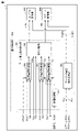
- FIG. 5 is a block diagram showing a detailed configuration example of the circulating current command value generation unit of FIG.
- the circulating current command value generation unit 510 includes a voltage average value generation unit 511, an intergroup voltage control unit 515, and a subtraction unit 514.
- the voltage average value generation unit 511 receives the capacitor voltage Vc detected by the voltage detector 33 from each converter cell 7.
- the voltage average value generation unit 511 predeterminedly determines from the capacitor voltage Vc of each converter cell 7 to the total voltage average value Vcall indicating the average value of the stored energies of the capacitors 32 of all the converter cells 7 of the power converter 2.
- the voltage average value Vcgr for each group which is the average value of the stored energy of the capacitor 32 of the converter cell 7 for each group, is generated.
- the voltage mean value Vcgr for each group is a plurality of (2 ⁇ Necll) converter cells 7 included in each of the leg circuits 4u (U phase), 4v (V phase), and 4w (W phase).
- the U-phase voltage average value Vcgu, the V-phase voltage average value Vcgv, and the W-phase voltage average value Vcgw indicating the average value of the stored energy are included.
- the voltage mean value Vcgr for each group is replaced with or in addition to the voltage mean value for each leg circuit 4 (U phase, V phase, W phase), and the upper arm 5 and the lower arm 6 are used for each leg circuit 4.
- the voltage average value Vcgr for each group indicating the average value of the stored energies of the plurality of (Necll) converter cells included in each arm may be included. That is, the voltage average value Vcgr for each group is U phase upper arm voltage average value Vcgup, U phase lower arm voltage average value Vcgun, V phase upper arm voltage average value Vcgbp, V phase lower arm voltage average value Vcgvn, W phase upper arm.
- the voltage mean value Vcgwp and the W phase lower arm voltage mean value Vcgwn may be included.
- the inter-group voltage control unit 515 balances the stored energy between the groups (between each phase leg circuit or between the arms) based on the group-by-group voltage mean value Vcgr generated by the voltage mean value generation unit 511.
- the circulating current command value Izref for compensating for the above is generated for each phase. That is, the intergroup voltage control unit 515 generates the U-phase circulating current command value Izrefu, the V-phase circulating current command value Izrefv, and the W-phase circulating current command value Izrefw.
- the subtraction unit 514 subtracts the voltage average value Vcgr for each group from the total voltage average value Vcall. For example, when the U-phase circulating current command value Izrefu is generated, the U-phase voltage mean value Vcgu is input to the subtraction unit 514 as the group-by-group voltage mean value Vcgr, and the U-phase upper arm voltage mean value Vcgup and The U-phase lower arm voltage average value Vcgun may be input.
- the intergroup voltage control unit 515 generates the u-phase circulating current command value Izrefu by performing an operation on the deviation of the U-phase voltage average value Vcgu with respect to the total voltage average value Vcall calculated by the subtraction unit 514.
- the intergroup voltage control unit 515 has a deviation of the U-phase voltage average value Vcgu with respect to the total voltage average value Vcall, a deviation of the U-phase upper arm voltage average value Vcguup with respect to the total voltage average value Vcall, and a U with respect to the total voltage average value Vcall.
- An operation is performed for each deviation of the mean value Vcgun of the lower arm voltage, and the u-phase circulating current command value Izrefu is generated by adding the operation results.
- the circulating current command value Izref equalizes the level of the capacitor voltage Vc of the converter cell 7 between the groups (between the leg circuits and even between the arms for each phase), and the stored energy in the converter cell 7 between the groups. Corresponds to the circulating current value for eliminating the imbalance of.
- the intergroup voltage control unit 515 can be configured as a PI controller that performs proportional calculation and integral calculation with respect to the deviation calculated by the subtraction unit 514, or is further configured as a PID controller that performs differential calculation. You can also do it. Alternatively, it is also possible to configure the intergroup voltage control unit 515 by using the configuration of another controller generally used for feedback control.
- FIG. 6 is a diagram showing a more detailed configuration of each basic control unit 502 of FIG.
- the basic control unit 502 includes an arm voltage command generation unit 601 and a capacitor voltage command generation unit 602.
- the arm voltage command generation unit 601 has a voltage command value krefp of Ncell converter cells 7 included in the upper arm 5 of FIG. 1 and a voltage command value krefn of Ncell converter cells 7 included in the lower arm 6. To generate.
- the arm voltage command generation unit 601 outputs the generated voltage command value krefp to the upper arm control unit 503P, and outputs the generated voltage command value krefn to the lower arm control unit 503N.
- the voltage command value krefp for the upper arm 5 and the voltage command value krefn for the lower arm 6 are collectively referred to as a voltage command value kref.
- the capacitor voltage command generation unit 602 generates the capacitor voltage command value Vcrefp of the capacitors 32 of the Ncell converter cells 7 included in the upper arm 5.
- the capacitor voltage command generation unit 602 further calculates the capacitor voltage command value Vcrefn of the capacitors 32 of the Ncell converter cells 7 included in the lower arm 6.
- the capacitor voltage command generation unit 602 outputs the generated capacitor voltage command value Vcrefp for the upper arm 5 to the upper arm control unit 503P, and outputs the generated capacitor voltage command value Vcrefn for the lower arm 6 to the lower arm control unit 503N. Output to.
- the capacitor voltage command value Vcrefp for the upper arm 5 is, for example, the average voltage of the capacitor 32 of the converter cell 7 of the upper arm
- the capacitor voltage command value Vcrefn for the lower arm 6 is, for example, the conversion of the lower arm 6. Let it be the average voltage of the capacitor 32 of the instrument cell 7.
- the capacitor voltage command value Vcrefp for the upper arm 5 and the capacitor voltage command value Vcrefn for the lower arm 6 are collectively referred to as a capacitor voltage command value Vcref.
- the arm voltage command generation unit 601 includes an AC current control unit 603, a DC current control unit 604, a circulating current control unit 605, a command distribution unit 606, and a discharge control unit. It is equipped with 607.
- the AC current control unit 603 calculates the AC control command value Vcr for making the deviation between the detected AC current Iac and the set AC current command value Iacref 0. Alternatively, the AC current control unit 603 calculates the AC control command value Vcr for making the deviation between the detected AC current Iac and the AC current command value Iacref changed by the discharge control unit 607 zero.
- the AC current control unit 603 can be configured as a PI controller that performs proportional calculation and integral calculation with respect to the deviation, and can also be configured as a PID controller that performs differential calculation. Alternatively, it is also possible to configure the AC current control unit 603 by using the configuration of another controller generally used for feedback control.
- the DC current control unit 604 sets the deviation between the detected DC current Idc and the set DC current command value Idcref to 0 based on the set DC voltage command value Vdcref and the set DC current command value Idcref.
- the DC control command value Vdcr for this is calculated.
- the DC voltage command value Vdcref may be calculated based on the detected DC voltage Vdc.
- the circulation current control unit 605 sets a circulation control command value Vzr for controlling the detected circulation current Iz according to the set circulation current command value Izref or the circulation current command value Izref changed by the discharge control unit 607. calculate.
- the set value of the circulating current command value Izref is set to, for example, 0. The operation of the discharge control unit 607 will be described later.
- the command distribution unit 606 receives an AC control command value Vcr, a circulation control command value Vzr, a DC control command value Vdcr, a neutral point voltage Vsn, and an AC voltage Vsys. Since the AC side of the power converter 2 is connected to the AC circuit 12 via the transformer 13, the neutral point voltage Vsn can be obtained from the voltage of the DC power supply of the DC circuit 14.
- the DC control command value Vdcr may be determined by DC output control or may be a constant value.
- the command distribution unit 606 calculates the voltage shared by the output of the upper arm and the lower arm based on these inputs.
- the command distribution unit 606 determines the arm voltage command value krefp of the upper arm and the arm voltage command value krefn of the lower arm by subtracting the voltage drop due to the inductance components in the upper arm and the lower arm from the calculated voltage, respectively. ..
- the determined upper arm arm voltage command value krefp and lower arm arm voltage command value krefn cause the AC current Iac to follow the AC current command value Iacref, the circulating current Iz to follow the circulating current command value Izref, and the DC voltage.
- This is an output voltage command that causes Vdc to follow the DC voltage command value Vdcref and feed-forward controls the AC voltage Vsys.
- a signal OM indicating the operation mode of the control device 3 is input to the discharge control unit 607.
- the MMC requires the effective value of the circulating current Iz to continue the operation of the power converter in order to minimize the loss of the power converter 2 in the normal operation mode (also referred to as the first operation mode). Control to the minimum value.
- the MMC of the present embodiment controls the effective value of the circulating current Iz in the discharge operation mode (also referred to as the second operation mode) so as to be larger than in the case of normal control. Since a resistance component exists inside the power converter 2, the loss increases by passing the circulating current Iz. This promotes the discharge of the capacitor 32 of each converter cell 7.
- the discharge control unit 607 changes the circulating current command value Izref so that the effective value of the circulating current Iz becomes larger than usual when the operation mode is switched from the normal operation mode to the discharge operation mode. More specifically, the discharge control unit 607 adds and corrects the discharge control output value to the circulating current command value Izref in the normal operation mode.
- the circulating current Iz When the circulating current Iz is intentionally passed, if the power converter 2 is connected to the AC power system (AC circuit 12), it is necessary to pass the circulating current Iz at a frequency other than the frequency of the system voltage. When the line is disconnected from the power system, it does not matter which frequency the circulating current is used. It is desirable that the frequency of the circulating current is high because the loss is expected to increase due to the skin effect.
- the discharge control unit 607 sets the amplitude value or the effective value of the AC current command value Iacref in the discharge operation mode to be smaller than in the normal operation mode. More specifically, the discharge control unit 607 subtracts and corrects the discharge control output value to the AC current command value Iacref.
- the function of the discharge control unit 607 may be included in each of the AC current control unit 603 and the circulation current control unit 605.
- the signal OM indicating the operation mode of the control device 3 is input to the alternating current control unit 603 and the circulating current control unit 605, respectively.
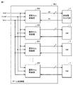
- FIG. 7 is a block diagram illustrating a configuration example of the arm control unit 503.
- the arm control unit 503 includes Ncell individual cell control units 202.
- the individual cell control unit 202 individually controls the corresponding converter cell 7.
- the individual cell control unit 202 receives the arm voltage command value kref, the arm current Iarm, and the capacitor voltage command value Vcref from the basic control unit 502.
- the individual cell control unit 202 generates the gate signal ga of the corresponding converter cell 7 and outputs it to the corresponding converter cell 7.
- each individual cell control unit 202 receives the detection value of the capacitor voltage Vc from the voltage detector 33 of the corresponding converter cell 7. Further, the detection value of the capacitor voltage Vc from the voltage detector 33 of each converter cell 7 is input to the basic control unit 502.
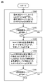
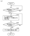
- FIG. 8 is a flowchart for explaining the switching timing from the normal operation mode to the discharge operation mode. In the initial state, it is assumed that the control device 3 is operating in the normal operation mode.
- step S100 when at least one capacitor voltage Vc exceeds the threshold value Vth (YES in step S100), the control device 3 advances the process to step S110.
- step S110 the control device 3 switches the operation mode from the normal operation mode to the discharge operation mode.
- step S210 the control device 3 switches the operation mode from the normal operation mode to the discharge operation mode.
- FIG. 9 is a flowchart for explaining the operation of the circulating current control unit, the discharge control unit, and the AC current control unit of FIG. 6 in the discharge operation mode.
- step S300 of FIG. 9 in the case of the normal operation mode, the AC current control unit 603 is based on the deviation between the detected AC current Iac and the AC current command value Iacref in the normal operation mode. Then, the AC control command value Vcr is generated. Further, the circulation control command value Vzr generates the circulation control command value Vzr based on the deviation between the detected circulation current Iz and the circulation current command value Izref in the normal operation mode described with reference to FIG. When the normal operation mode is continued (NO in step S310), the above step S300 is repeated.
- step S310 When the normal operation mode is switched to the discharge operation mode (YES in step S310), the control device 3 advances the process to steps S320 and S330. Either of steps S320 and S330 may be executed first, or may be executed in parallel.
- step S320 the AC current control unit 603 sets the effective value or amplitude value of the AC current command value Iacref to be smaller than in the normal operation mode, and calculates the AC control command value Vcr.
- step S330 the circulation current control unit 605 sets the effective value or the amplitude value of the circulation current command value Izref to be larger than that in the normal operation mode, and calculates the circulation control command value Vzr.
- the circulating current control unit 605 changes the circulating control command value Vzr so that the effective value or the amplitude value of the circulating current Iz becomes larger than in the normal operation mode without changing the circulating current command value Izref. You may.
- step S340 When the discharge operation mode is continued (NO in step S340), the above steps S320 and S330 are repeated.
- the control device 3 returns the process to step S300.
- the effective value or amplitude value of the circulating current Iz is the minimum value required to continue the operation of the power converter 2 in order to minimize the loss of the power converter 2. Is controlled.
- the control device 3 when the operation mode is switched from the normal operation mode to the discharge operation mode, the control device 3 has an effective value or an amplitude value of the circulating current Iz as compared with the case of the normal operation mode.
- the power converter 2 is controlled so as to be large. Since the resistance component exists inside the power converter 2, the loss increases by passing the circulating current Iz, which can promote the discharge of the capacitor 32 of each converter cell 7.
- the discharge control unit 607 corrects the circulation current command value Izref or the circulation control command value Vzr so that the effective value or the amplitude value of the circulation current Iz becomes larger in the discharge operation mode than in the normal operation mode. do. More specifically, the discharge control unit 607 adds and corrects the discharge control output to the circulating current command value Izref.
- the circulating current Iz When the circulating current Iz is intentionally passed, if the power converter 2 is connected to the AC power system (AC circuit 12), it is necessary to pass the circulating current Iz at a frequency other than the frequency of the system voltage. When the power converter 2 is disconnected from the AC power system (AC circuit 12), there is no problem in using any frequency of the circulating current Iz. It is desirable that the frequency of the circulating current Iz is high because the loss is expected to increase due to the skin effect.
- Embodiment 2 the power converter 2 is controlled so as to increase the effective value or the amplitude value of the circulating current Iz as much as possible within the range of the safe operating area (SOA).
- SOA means a range of voltage and current at which the semiconductor element used as the switching element 31 of the converter cell 7 can safely switch.
- FIG. 10 is a diagram conceptually showing an example of SOA of an IGBT or MOSFET.
- the vertical axis of FIG. 10 shows the collector current Ic
- the horizontal axis of FIG. 10 shows the collector-emitter voltage Vce.
- the collector current Ic corresponds to the arm current Iarm flowing through each arm
- the collector-emitter voltage Vce corresponds to the capacitor voltage Vc of each converter cell 7.
- the upper limit of the collector current Ic is a constant value Imax. While the collector-emitter voltage Vce is from V2 to Vmax, the allowable collector current Ic becomes smaller as the collector-emitter voltage Vce increases. In this way, the upper limit of the collector current Ic changes according to the collector-emitter voltage Vce.
- the magnitude of the circulating current Iz is determined by determining the magnitude of the effective value or the amplitude value of the circulating current Iz so that the peak value of the arm current Iarm matches the upper limit value of the SOA according to the capacitor voltage Vc. You can increase as much as possible. Further, since the arm current Iarm is determined by the sum of the AC current Iac, the DC current Idc, and the circulating current Iz, in order to set the amplitude value or the effective value of the circulating current Iz larger, the amplitude of the AC current command value Iacref. It is desirable to set the value or effective value smaller than in the normal operation mode.
- the amplitude value or effective value of the circulating current Iz is determined so that the peak value of the arm current Iarm coincides with I1.
- the upper limit of the arm current Iarm increases. Therefore, the effective value or the amplitude value of the circulating current Iz is increased according to the magnitude of the capacitor voltage Vc.
- the capacitor 32 can be discharged safely and at high speed.
- the circulating current control unit 605 determines the effective value or the amplitude value of the circulating current Iz so that the peak value of the arm current Iarm matches the upper limit value Imax of the SOA.
- FIG. 11 is a flowchart for explaining the operation of the circulating current control unit, the discharge control unit, and the AC current control unit in the discharge operation mode in the power conversion device of the second embodiment.
- the flowchart of FIG. 11 differs from the flowchart of FIG. 9 in that step S330 is changed to step S330A. Since the other steps in FIG. 11 are the same as in the case of FIG. 9, the same or corresponding steps are designated by the same reference numerals and the description is not repeated.
- the circulating current control unit 605 determines the effective value or amplitude value of the circulating current command value Izref so that the peak value of the arm current Iarm becomes equal to the upper limit value of SOA according to the decrease of the capacitor voltage Vc. To determine. Alternatively, the circulation current control unit 605 does not change the circulation current command value Izref, and the circulation control command value Vzr so that the peak value of the arm current Iarm becomes equal to the upper limit value of the SOA according to the decrease in the capacitor voltage Vc. May be changed.
- the control device 3 is a power converter in the discharge operation mode so as to increase the effective value or the amplitude value of the circulating current Iz as much as possible within the range of SOA. 2 is controlled.
- the capacitor 32 can be discharged at the fastest speed without damaging the switching element 31 of each converter cell 7.
- Embodiment 3 In the power conversion device 1 of the third embodiment, the carrier frequency in the pulse width control is increased in the discharge operation mode. As a result, the switching loss of the switching element 31 can be increased, so that the discharge of the capacitor 32 can be accelerated.
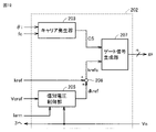
- FIG. 12 is a block diagram showing a configuration example of the individual cell control unit 202 shown in FIG. 7.
- the individual cell control unit 202 includes a carrier generator 203, an individual voltage control unit 205, an adder 206, and a gate signal generation unit 207.
- the carrier generator 203 generates a carrier signal CS having a predetermined frequency (that is, carrier frequency) used in phase shift PWM (Pulse Width Modulation) control.
- the phase shift PWM control shifts the timing of the PWM signals output to each of the plurality of (Ncell) converter cells 7 constituting the same arm (upper arm 5 or lower arm 6). .. It is known that this reduces the harmonic components included in the combined voltage of the output voltage of each converter cell 7.
- the carrier generator 203 generates carrier signals CS that are out of phase with each other among the Ncell converter cells 7 based on the common reference phase ⁇ i and carrier frequency fc received from the basic control unit 502.
- the individual voltage control unit 205 receives the capacitor voltage command value Vcref, the capacitor voltage Vc of the corresponding converter cell 7, and the detected value of the arm current Iarm of the arm to which the corresponding converter cell 7 belongs.
- the capacitor voltage command value Vcref may be set to the average value of the entire capacitor voltage Vc of the power converter 2, or may be set to the average value of the capacitor voltages of Ncell converter cells 7 included in the same arm. May be good.
- the individual voltage control unit 205 calculates the control output dkref for individual voltage control by calculating the deviation of the capacitor voltage Vc with respect to the capacitor voltage command value Vcref.
- the individual voltage control unit 205 can also be configured by a controller that executes PI control, PID control, or the like. Further, by multiplying the calculated value by the controller by "+1" or "-1" according to the polarity of the arm current Iarm, the capacitor 32 is charged and discharged in the direction of eliminating the deviation.
- the control output dkref is calculated.
- the control output dkref for charging / discharging the capacitor 32 may be calculated by multiplying the calculated value by the controller by the arm current Iarm in the direction of eliminating the deviation.
- the adder 206 outputs the cell voltage command value krefc by adding the arm voltage command value kref from the basic control unit 502 and the control output dkref of the individual voltage control unit 205.
- the gate signal generation unit 207 generates a gate signal ga by PWM-modulating the cell voltage command value krefc by the carrier signal CS from the carrier generator 203.
- FIG. 13 is a conceptual waveform diagram for explaining PWM modulation control by the gate signal generation unit shown in FIG.
- the signal waveform shown in FIG. 13 is exaggerated for the sake of explanation, and does not show the actual signal waveform as it is.
- the cell voltage command value krefc is typically voltage-compared with the carrier signal CS composed of a triangular wave.
- the PWM modulation signal Spwm is set to a high level (H level).
- the PWM modulation signal Spwm is set to the low level (L level).
- the switching elements 31p and 31n of the converter cell 7 are on / off controlled by being sent to the gate driver (not shown) of the switching elements 31p and 31n of the converter cell 7 as the gate signal ga.
- the cell voltage command value krefc corresponds to the sinusoidal voltage corrected by the control output dkref. Therefore, in the control device 3, the modulation factor command value in PWM modulation is calculated from the amplitude (or effective value) of the sinusoidal voltage (arm voltage command value kref) and the amplitude of the carrier signal CS by a known method. It is possible.
- FIG. 14 is a flowchart for explaining the setting of the carrier frequency in the power converter according to the third embodiment. In the initial state, it is assumed that the control device 3 is in the normal operation mode.
- step S410 the control device 3 sets the carrier frequency fc to be larger than that in the normal operation mode.
- step S410 If the discharge operation mode is maintained (NO in step S410), the above step S410 is continued. On the other hand, when switching from the discharge operation mode to the normal operation mode (YES in step S410), in the next step S430, the control device 3 returns the carrier frequency fc to the set value of the original normal operation mode.
- the control device 3 sets the carrier frequency fc in the phase shift PWM control to a larger value in the discharge operation mode than in the normal operation mode. As a result, the switching loss in the switching element 31 of the converter cell 7 can be increased, so that the discharge of the capacitor 32 can be accelerated.
- Embodiment 4 In the power conversion device 1 of the fourth embodiment, the loss of the switching element 31 in the discharge operation mode is increased by using the active gate drive. As a result, the discharge of the capacitor 32 can be accelerated.
- the fourth embodiment can be combined with any of the second and third embodiments.
- FIG. 15 is a circuit diagram showing a configuration example of a converter cell constituting the power converter in the power converter according to the fourth embodiment.
- the converter cell 7 includes a gate driver capable of an active gate drive of the switching element 31.
- the circuit diagram (A) of FIG. 15 is different from the circuit diagram (A) of FIG. 2 in that the gate resistors 34p and 34n whose resistance values are variable according to the control signal act are further provided.
- the circuit diagram (B) of FIG. 15 differs from the circuit diagram (B) of FIG. 2 in that it further includes a gate resistor 34p1, 34p2, 34n1, 34n2 whose resistance value is variable according to the control signal act. Since the other points of FIG. 15 are the same as those of FIG. 2, the same or corresponding parts are designated by the same reference numerals and the description is not repeated.
- gate resistors 34 when the gate resistors 34p, 34n and the gate resistors 34p1, 34p2, 34n1, 34n2 are generically referred to or unspecified, they are referred to as gate resistors 34.
- a variable resistor is provided as the gate resistor 34, but the gate resistor 34 may be configured to change the resistance value by switching the connection of a plurality of resistors.
- FIG. 16 is a block diagram showing a configuration example of an individual cell control unit in the power conversion device of the fourth embodiment.
- the individual cell control unit 202 of FIG. 16 is different from the individual cell control unit 202 of FIG. 12 in that the gate drive control unit 208 is further included. Since the other points of FIG. 16 are the same as those of FIG. 12, the same or corresponding parts are designated by the same reference numerals and the description is not repeated.
- the gate drive control unit 208 of the individual cell control unit 202 activates the control signal act when the operation mode of the control device 3 is switched from the normal operation mode to the discharge operation mode. ..
- the gate drive control unit 208 increases the gate resistance value of the corresponding converter cell 7.
- the switching time of the switching element 31 of the converter cell 7 increases, so that the switching loss increases, so that the discharge of the capacitor 32 can be accelerated.
- the method of active gate drive is not limited to the method of changing the gate resistance as long as it changes the switching loss of the switching element 31.
- the switching time may be increased by a method other than increasing the gate resistance value.
- FIG. 17 is a flowchart for explaining the setting of the gate resistance in the power converter according to the fourth embodiment. In the initial state, it is assumed that the control device 3 is in the normal operation mode.
- step S500 When switching from the normal operation mode to the discharge operation mode (YES in step S500), the control device 3 advances the process to step S510.
- step S510 the control device 3 sets the resistance value of the gate resistor 34 provided corresponding to the switching element 31 of each converter cell 7 to be larger than that in the normal operation mode.
- step S510 If the discharge operation mode is maintained (NO in step S510), the above step S510 is continued. On the other hand, when switching from the discharge operation mode to the normal operation mode (YES in step S510), in the next step S530, the control device 3 returns the gate resistance value to the set value of the original normal operation mode.
- the control device 3 uses the active gate drive in the discharge operation mode to increase the loss of the switching element 31 as compared with the case of the normal operation mode.
- Each converter cell 7 is controlled in such a manner. As a result, the discharge of the capacitor 32 can be accelerated.
- Embodiment 5 In MMC, it is common to provide a charging resistor between the power converter 2 and the AC system in order to suppress the charging current at the time of starting. In the power conversion device 1 of the fifth embodiment, the charge resistor is provided in each arm to increase the loss due to the circulating current Iz flowing in the discharge operation mode.
- the fifth embodiment can be combined with any of the second to fourth embodiments.
- FIG. 18 is a schematic configuration diagram of the power conversion device in the power conversion device 1 of the fifth embodiment.
- Each upper arm 5 of FIG. 18 further includes a charging resistor 18A provided in series with the plurality of converter cells 7 and the reactor 8A, and a bypass switch 15A connected in parallel with the charging resistor 18A. It is different from each upper arm 5 of 2.
- each lower arm 6 of FIG. 18 further includes a charging resistor 18B provided in series with the plurality of converter cells 7 and the reactor 8B, and a bypass switch 15B connected in parallel with the charging resistor 18B. It differs from each lower arm 6 in FIG. 2 in that it is different from each lower arm 6 in FIG.
- charging resistors 18A and 18B When the charging resistors 18A and 18B are generically referred to or when they indicate unspecified ones, they are referred to as charging resistors 18. Further, the bypass switch 15A and 15B are referred to as a bypass switch 15 when they are generically referred to or when they indicate an unspecified one. Since the other points of FIG. 18 are the same as those of FIG. 1, the same or corresponding parts are designated by the same reference numerals and the description is not repeated.
- FIG. 19 is a functional block diagram illustrating the internal configuration of the control device 3 in the power conversion device 1 of the fifth embodiment.
- the control device 3 of FIG. 19 is different from the control device 3 of FIG. 4 in that it further includes a charge resistance control unit 504 for controlling the bypass switch 15. Since the other points in FIG. 19 are the same as in the case of FIG. 4, the same or corresponding parts are designated by the same reference numerals and the description is not repeated.
- the charge resistance control unit 504 controls the bypass switch 15 in the closed state in the normal operation mode. As a result, the arm current Iarm is bypassed, so that the loss increase of the power converter 2 due to the charge resistor 18 can be prevented.
- the charge resistance control unit 504 opens the bypass switch 15 in the discharge operation mode. As a result, the arm current Iarm flows through the charge resistor 18, so that the loss of the power converter 2 can be increased.
- FIG. 20 is a flowchart illustrating the operation of the charge resistance control unit.
- the flowchart (A) of FIG. 20 shows the operation of the charge resistance control unit 504 when the power converter 2 is started, and the flowchart (B) of FIG. 20 shows the operation of the charge resistance control unit 504 in the discharge operation mode.
- step S600 the control device 3 advances the process to step S610.
- step S610 the charge resistance control unit 504 of the control device 3 opens each bypass switch 15. As a result, the charging current of the capacitor 32 of each converter cell 7 is suppressed.
- the control device 3 determines that the charging of the capacitor 32 is completed (YES in step S620). In this case, in the next step S630, the charge resistance control unit 504 of the control device 3 closes each bypass switch 15.
- control device 3 is in the normal operation mode and each bypass switch 15 is in the closed state in the initial state.
- step S700 When switching from the normal operation mode to the discharge operation mode (YES in step S700), the control device 3 advances the process to step S710.
- step S710 the charge resistance control unit 504 of the control device 3 opens each bypass switch 15. As a result, the arm current Iarm flows through the charge resistor 18 and the loss of the power converter 2 increases, so that the discharge of the capacitor 32 can be accelerated.
- step S720 When switching from the discharge operation mode to the normal operation mode (YES in step S720), the control device 3 advances the process to step S730. In step S730, the charge resistance control unit 504 of the control device 3 closes each bypass switch 15.
- the charge resistor 18 provided on each arm is used to increase the loss due to the circulating current Iz in the discharge operation mode. As a result, the discharge of the capacitor 32 in the discharge operation mode can be accelerated.
Landscapes
- Engineering & Computer Science (AREA)
- Power Engineering (AREA)
- Inverter Devices (AREA)
Abstract
Description
[電力変換装置の全体構成]
図1は、実施の形態1の電力変換装置の概略構成図である。図1を参照して、電力変換装置1は、互いに直列接続された複数の変換器セルを含むモジュラーマルチレベル変換器(MMC)によって構成されている。なお、「変換器セル」は、「サブモジュール」、「SM」、または「単位変換器」とも呼ばれる。電力変換装置1は、直流回路14と交流回路12との間で電力変換を行なう。電力変換装置1は、電力変換器2と、制御装置3とを含む。
交流電圧検出器10は、交流回路12のU相の交流電圧Vsysu、V相の交流電圧Vsysv、および、W相の交流電圧Vsyswを検出する。以下の説明では、Vsysu、Vsysv、および、Vsyswを総称してVsysとも記載する。電力変換器2の交流入力端子Nu,Nv,Nwの交流電圧Vacu,Vacv,Vacwは、交流電圧検出器10で検出される交流電圧Vsysu,Vsysv,Vsyswから、変圧器13の変圧比およびインピーダンス降下を考慮して求めることができる。以下の説明では、交流Vacu、Vacv、およびVacwを総称してVacとも記載する。
Iacu=Ipu-Inu …(1)
Iacv=Ipv-Inv …(2)
Iacw=Ipw-Inw …(3)
のように表される。以下の説明では、Iacu、Iacv、およびIacwを総称して、Iacとも記載する。
Idc=(Ipu+Inu+Ipv+Inv+Ipw+Inw)/2 …(4)
と表される。
Izu=(Ipu+Inu)/2-Idc/3 …(5)
Izv=(Ipv+Inv)/2-Idc/3 …(6)
Izw=(Ipw+Inw)/2-Idc/3 …(7)
のように定義できる。各相の循環電流Izu,Izv,Izwを総称してIzと記載する。
図2は、電力変換器を構成する変換器セルの構成例を示す回路図である。
図3は、制御装置3のハードウェア構成例を示すブロック図である。図3には、コンピュータによって制御装置3を構成する例が示される。
以下、放電運転モードにおける電力変換器2の制御手順について、これまでの説明を総括する。
通常のMMCの制御では、電力変換器2の損失を最小限にするために、循環電流Izの実効値または振幅値は、電力変換器2の運転を継続するために必要な最小の値になるように制御される。
実施の形態2では、安全運転領域(SOA:Safety Operating Area)の範囲内で、できるだけ循環電流Izの実効値または振幅値を大きくするように、電力変換器2を制御する。これにより、各変換器セル7のキャパシタ32の放電を早めることができる。ここで、SOAとは、変換器セル7のスイッチング素子31として用いられている半導体素子が安全にスイッチングを行うことができる電圧と電流の範囲をいう。
図10は、IGBTまたはMOSFETのSOAの一例を概念的に示す図である。図10の縦軸はコレクタ電流Icを示し、図10の横軸はコレクタエミッタ電圧Vceを示す。コレクタ電流Icは各アームを流れるアーム電流Iarmに対応し、コレクタエミッタ電圧Vceは各変換器セル7のキャパシタ電圧Vcに対応する。
図11は、実施の形態2の電力変換装置において、放電運転モードにおける循環電流制御部、放電制御部、および交流電流制御部の動作を説明するためのフローチャートである。図11のフローチャートは、ステップS330がステップS330Aに変更された点で図9のフローチャートと異なる。図11のその他のステップは図9の場合と同様であるので、同一または相当するステップには同一の参照符号を付して説明を繰り返さない。
以上のとおり、実施の形態2の電力変換装置1によれば、制御装置3は、放電運転モードにおいて、SOAの範囲内でできるだけ循環電流Izの実効値または振幅値を大きくするように電力変換器2を制御する。これによって、各変換器セル7のスイッチング素子31を破損させることなく、最速でキャパシタ32の放電を行うことができる。
実施の形態3の電力変換装置1では、放電運転モードにおいて、パルス幅制御におけるキャリア周波数を増大させる。これによってスイッチング素子31のスイッチング損失を増大させることができるので、キャパシタ32の放電を早めることができる。
図12を参照して、個別セル制御部202は、キャリア発生器203と、個別電圧制御部205と、加算器206と、ゲート信号生成部207とを備える。
図14は、実施の形態3の電力変換器におけるキャリア周波数の設定について説明するためのフローチャートである。初期状態において、制御装置3は通常運転モードであるとする。
以上のとおり、実施の形態3の電力変換装置1によれば、制御装置3は、放電運転モードにおいて、位相シフトPWM制御におけるキャリア周波数fcを通常運転モードの場合より大きな値に設定する。これによって、変換器セル7のスイッチング素子31におけるスイッチング損失を増大させることができるので、キャパシタ32の放電を早めることができる。
実施の形態4の電力変換装置1では、アクティブゲートドライブを用いることによって、放電運転モードにおけるスイッチング素子31の損失を増大させる。これによって、キャパシタ32の放電を早めることができる。以下、図面を参照して具体的に説明する。なお、実施の形態4は、実施の形態2,3のいずれとも組み合わせることができる。
図15は、実施の形態4の電力変換装置において、電力変換器を構成する変換器セルの構成例を示す回路図である。実施の形態4の場合には、変換器セル7は、スイッチング素子31のアクティブゲートドライブが可能なゲートドライバを備える。
図17は、実施の形態4の電力変換器におけるゲート抵抗の設定について説明するためのフローチャートである。初期状態において、制御装置3は通常運転モードであるとする。
以上のとおり、実施の形態4の電力変換装置1によれば、制御装置3は、放電運転モードにおいて、アクティブゲートドライブを用いることにより、スイッチング素子31の損失を通常運転モードの場合よりも増大させるように各変換器セル7を制御する。これにより、キャパシタ32の放電を早めることができる。
MMCでは、起動時の充電電流を抑制するために、電力変換器2と交流系統との間に充電抵抗器を設けることが一般的である。実施の形態5の電力変換装置1では、充電抵抗器を各アームに設けることにより、放電運転モードにおいて流す循環電流Izによる損失を増大させる。以下、図面を参照して詳しく説明する。なお、実施の形態5は、実施の形態2~4のいずれとも組み合わせることができる。
図18は、実施の形態5の電力変換装置1における電力変換装置の概略構成図である。
図20は、充電抵抗制御部の動作を説明するフローチャートである。図20のフローチャート(A)は、電力変換器2の起動時の充電抵抗制御部504の動作を示し、図20のフローチャート(B)は、放電運転モードにおける充電抵抗制御部504の動作を示す。
以上のとおり、実施の形態5の電力変換装置1によれば、各アームに設けられた充電抵抗器18を利用して放電運転モード時に循環電流Izによる損失を増大させる。これによって、放電運転モードにおけるキャパシタ32の放電を早めることができる。
Claims (9)
- 互いにカスケード接続された複数の変換器セルを有するアームを複数含む電力変換器と、
前記電力変換器を制御する制御装置とを備え、
前記複数のアームの各々は、交流回路の対応する相と電気的に接続され、
前記複数の変換器セルの各々は、
一対の入出力端子と、
複数のスイッチング素子と、
前記複数のスイッチング素子を介して前記入出力端子と電気的に接続される蓄電素子とを含み、
前記制御装置は、
前記電力変換器と前記交流回路との間を流れる交流電流を制御する交流電流制御部と、
前記電力変換器の前記アーム間を流れる循環電流を制御する循環電流制御部とを含み、
前記循環電流制御部は、第1の運転モードにおいて、異なる前記アーム間での前記蓄電素子の電圧の不均衡を解消するように、前記循環電流を制御し、
前記循環電流制御部は、第2の運転モードにおいて、前記第1の運転モードの場合よりも前記循環電流の実効値または振幅値を増加させることにより、前記電力変換器を構成する各前記変換器セルの前記蓄電素子の電圧を低下させ、
前記交流電流制御部は、前記第2の運転モードにおいて、前記第1の運転モードの場合よりも前記交流電流の実効値または振幅値を減少させる、電力変換装置。 - 前記循環電流制御部は、前記第2の運転モードにおいて、前記蓄電素子の電圧の低下に応じて前記循環電流の実効値または振幅値を変化させる、請求項1に記載の電力変換装置。
- 前記循環電流制御部は、前記第2の運転モードにおいて、各前記変換器セルの各前記スイッチング素子の安全動作領域で決まる電流の上限値にアーム電流のピーク値が一致するように、前記循環電流の実効値または振幅値を変化させる、請求項2に記載の電力変換装置。
- 前記制御装置は、位相シフトパルス幅変調によって各前記変換器セルの出力電圧を制御し、
前記制御装置は、前記第2の運転モードにおいて、前記位相シフトパルス幅変調のキャリア周波数を、前記第1の運転モードの場合よりも増加させる、請求項1~3のいずれか1項に記載の電力変換装置。 - 各前記変換器セルに設けられた各前記スイッチング素子のスイッチング損失は、前記制御装置からの制御によって変化し、
前記制御装置は、前記第2の運転モードにおいて、各前記変換器セルに設けられた各前記スイッチング素子のスイッチング損失を、前記第1の運転モードの場合よりも増加させる、請求項1~4のいずれか1項に記載の電力変換装置。 - 各前記変換器セルに設けられた各前記スイッチング素子のゲート抵抗値は、前記制御装置からの制御によって変化し、
前記制御装置は、前記第2の運転モードにおいて、前記ゲート抵抗値を前記第1の運転モードの場合よりも増加させることによって前記スイッチング損失を増加させる、請求項5に記載の電力変換装置。 - 各前記アームは、前記複数の変換器セルと直列に接続された充電抵抗器と、前記充電抵抗器と並列に接続されたバイパススイッチとをさらに含み、
前記制御装置は、前記第2の運転モードにおいて前記バイパススイッチを開放状態にし、前記第1の運転モードにおいて前記バイパススイッチを閉状態にする、請求項1~6のいずれか1項に記載の電力変換装置。 - 前記制御装置は、前記複数の変換器セルに設けられた前記蓄電素子の少なくとも1つの電圧が閾値を超えている場合に、前記第1の運転モードから前記第2の運転モードに運転モードを切り替える、請求項1~7のいずれか1項に記載の電力変換装置。
- 前記制御装置は、前記電力変換器の運転停止指令を受けた場合に、前記第1の運転モードから前記第2の運転モードに運転モードを切り替える、請求項1~8のいずれか1項に記載の電力変換装置。
Priority Applications (4)
| Application Number | Priority Date | Filing Date | Title |
|---|---|---|---|
| PCT/JP2020/045900 WO2022123697A1 (ja) | 2020-12-09 | 2020-12-09 | 電力変換装置 |
| JP2021509941A JP6899987B1 (ja) | 2020-12-09 | 2020-12-09 | 電力変換装置 |
| US18/254,584 US12456932B2 (en) | 2020-12-09 | 2020-12-09 | Power conversion device |
| EP20965080.3A EP4262078A4 (en) | 2020-12-09 | 2020-12-09 | Power conversion device |
Applications Claiming Priority (1)
| Application Number | Priority Date | Filing Date | Title |
|---|---|---|---|
| PCT/JP2020/045900 WO2022123697A1 (ja) | 2020-12-09 | 2020-12-09 | 電力変換装置 |
Publications (1)
| Publication Number | Publication Date |
|---|---|
| WO2022123697A1 true WO2022123697A1 (ja) | 2022-06-16 |
Family
ID=76650093
Family Applications (1)
| Application Number | Title | Priority Date | Filing Date |
|---|---|---|---|
| PCT/JP2020/045900 Ceased WO2022123697A1 (ja) | 2020-12-09 | 2020-12-09 | 電力変換装置 |
Country Status (4)
| Country | Link |
|---|---|
| US (1) | US12456932B2 (ja) |
| EP (1) | EP4262078A4 (ja) |
| JP (1) | JP6899987B1 (ja) |
| WO (1) | WO2022123697A1 (ja) |
Families Citing this family (2)
| Publication number | Priority date | Publication date | Assignee | Title |
|---|---|---|---|---|
| WO2021181583A1 (ja) * | 2020-03-11 | 2021-09-16 | 三菱電機株式会社 | 電力変換装置 |
| CN120446580B (zh) * | 2025-07-10 | 2025-09-19 | 安擎计算机信息股份有限公司 | 一种测试系统功率的电路和方法 |
Citations (5)
| Publication number | Priority date | Publication date | Assignee | Title |
|---|---|---|---|---|
| JP2016100926A (ja) * | 2014-11-19 | 2016-05-30 | 三菱電機株式会社 | 電力変換装置 |
| WO2017046910A1 (ja) * | 2015-09-17 | 2017-03-23 | 三菱電機株式会社 | 電力変換装置 |
| JP2018093637A (ja) | 2016-12-05 | 2018-06-14 | 東芝三菱電機産業システム株式会社 | 電力変換装置 |
| WO2019138550A1 (ja) * | 2018-01-12 | 2019-07-18 | 三菱電機株式会社 | 電力変換装置 |
| JP6752401B1 (ja) * | 2020-03-11 | 2020-09-09 | 三菱電機株式会社 | 電力変換装置 |
Family Cites Families (6)
| Publication number | Priority date | Publication date | Assignee | Title |
|---|---|---|---|---|
| JP5881477B2 (ja) * | 2012-03-06 | 2016-03-09 | 三菱電機株式会社 | スイッチング素子駆動回路 |
| US10205402B2 (en) * | 2015-09-17 | 2019-02-12 | Mitsubishi Electric Corporation | Power conversion device for converting power between a DC circuit and an AC circuit by performing a non-linear operation |
| US10211827B2 (en) * | 2017-01-31 | 2019-02-19 | Ford Global Technologies, Llc | Resonant gate driver |
| JP6824103B2 (ja) * | 2017-04-25 | 2021-02-03 | 三菱電機株式会社 | 電力半導体装置および電力半導体駆動システム |
| JP6783419B1 (ja) * | 2020-03-30 | 2020-11-11 | 三菱電機株式会社 | 電力変換装置 |
| EP4170889A4 (en) * | 2020-06-17 | 2023-07-26 | Mitsubishi Electric Corporation | POWER CONVERTER |
-
2020
- 2020-12-09 JP JP2021509941A patent/JP6899987B1/ja active Active
- 2020-12-09 WO PCT/JP2020/045900 patent/WO2022123697A1/ja not_active Ceased
- 2020-12-09 US US18/254,584 patent/US12456932B2/en active Active
- 2020-12-09 EP EP20965080.3A patent/EP4262078A4/en active Pending
Patent Citations (5)
| Publication number | Priority date | Publication date | Assignee | Title |
|---|---|---|---|---|
| JP2016100926A (ja) * | 2014-11-19 | 2016-05-30 | 三菱電機株式会社 | 電力変換装置 |
| WO2017046910A1 (ja) * | 2015-09-17 | 2017-03-23 | 三菱電機株式会社 | 電力変換装置 |
| JP2018093637A (ja) | 2016-12-05 | 2018-06-14 | 東芝三菱電機産業システム株式会社 | 電力変換装置 |
| WO2019138550A1 (ja) * | 2018-01-12 | 2019-07-18 | 三菱電機株式会社 | 電力変換装置 |
| JP6752401B1 (ja) * | 2020-03-11 | 2020-09-09 | 三菱電機株式会社 | 電力変換装置 |
Non-Patent Citations (1)
| Title |
|---|
| See also references of EP4262078A4 |
Also Published As
| Publication number | Publication date |
|---|---|
| JP6899987B1 (ja) | 2021-07-07 |
| EP4262078A4 (en) | 2024-01-17 |
| JPWO2022123697A1 (ja) | 2022-06-16 |
| US20240022183A1 (en) | 2024-01-18 |
| US12456932B2 (en) | 2025-10-28 |
| EP4262078A1 (en) | 2023-10-18 |
Similar Documents
| Publication | Publication Date | Title |
|---|---|---|
| US12413156B2 (en) | Capacitor balancing control in an HVDC MMC | |
| US12273045B2 (en) | Power conversion device with individual cell and arm balancing | |
| JPWO2021048906A1 (ja) | 電力変換装置 | |
| JP7224468B2 (ja) | 電力変換装置 | |
| JP6768993B1 (ja) | 電力変換装置 | |
| JP6752401B1 (ja) | 電力変換装置 | |
| JP6797333B1 (ja) | 電力変換装置 | |
| US20260018991A1 (en) | Power conversion device and offshore wind power generation system | |
| JP6899987B1 (ja) | 電力変換装置 | |
| JP6771707B1 (ja) | 電力変換装置 | |
| JP6896201B1 (ja) | 電力変換装置 | |
| JP6873352B1 (ja) | 電力変換システムおよびその制御装置 | |
| JP6910579B1 (ja) | 電力変換システムおよびその制御装置 | |
| Zhang et al. | Four-Transistor Four-Diode (4T4D) Series/Parallel Chopper Module for Auto-Balancing STATCOM and Low Control and Development Complexity |
Legal Events
| Date | Code | Title | Description |
|---|---|---|---|
| ENP | Entry into the national phase |
Ref document number: 2021509941 Country of ref document: JP Kind code of ref document: A |
|
| 121 | Ep: the epo has been informed by wipo that ep was designated in this application |
Ref document number: 20965080 Country of ref document: EP Kind code of ref document: A1 |
|
| WWE | Wipo information: entry into national phase |
Ref document number: 18254584 Country of ref document: US |
|
| NENP | Non-entry into the national phase |
Ref country code: DE |
|
| ENP | Entry into the national phase |
Ref document number: 2020965080 Country of ref document: EP Effective date: 20230710 |
|
| WWG | Wipo information: grant in national office |
Ref document number: 18254584 Country of ref document: US |