WO2022123700A1 - 直流遮断器および直流遮断器システム - Google Patents
直流遮断器および直流遮断器システム Download PDFInfo
- Publication number
- WO2022123700A1 WO2022123700A1 PCT/JP2020/045906 JP2020045906W WO2022123700A1 WO 2022123700 A1 WO2022123700 A1 WO 2022123700A1 JP 2020045906 W JP2020045906 W JP 2020045906W WO 2022123700 A1 WO2022123700 A1 WO 2022123700A1
- Authority
- WO
- WIPO (PCT)
- Prior art keywords
- charging
- voltage
- circuit
- switch
- capacitor
- Prior art date
- Legal status (The legal status is an assumption and is not a legal conclusion. Google has not performed a legal analysis and makes no representation as to the accuracy of the status listed.)
- Ceased
Links
Images


Classifications
-
- H—ELECTRICITY
- H01—ELECTRIC ELEMENTS
- H01H—ELECTRIC SWITCHES; RELAYS; SELECTORS; EMERGENCY PROTECTIVE DEVICES
- H01H33/00—High-tension or heavy-current switches with arc-extinguishing or arc-preventing means
- H01H33/02—Details
- H01H33/59—Circuit arrangements not adapted to a particular application of the switch and not otherwise provided for, e.g. for ensuring operation of the switch at a predetermined point in the AC cycle
- H01H33/596—Circuit arrangements not adapted to a particular application of the switch and not otherwise provided for, e.g. for ensuring operation of the switch at a predetermined point in the AC cycle for interrupting DC
-
- H—ELECTRICITY
- H02—GENERATION; CONVERSION OR DISTRIBUTION OF ELECTRIC POWER
- H02H—EMERGENCY PROTECTIVE CIRCUIT ARRANGEMENTS
- H02H3/00—Emergency protective circuit arrangements for automatic disconnection directly responsive to an undesired change from normal electric working condition with or without subsequent reconnection ; integrated protection
- H02H3/08—Emergency protective circuit arrangements for automatic disconnection directly responsive to an undesired change from normal electric working condition with or without subsequent reconnection ; integrated protection responsive to excess current
- H02H3/087—Emergency protective circuit arrangements for automatic disconnection directly responsive to an undesired change from normal electric working condition with or without subsequent reconnection ; integrated protection responsive to excess current for DC applications
-
- H—ELECTRICITY
- H01—ELECTRIC ELEMENTS
- H01H—ELECTRIC SWITCHES; RELAYS; SELECTORS; EMERGENCY PROTECTIVE DEVICES
- H01H9/00—Details of switching devices, not covered by groups H01H1/00 - H01H7/00
- H01H9/54—Circuit arrangements not adapted to a particular application of the switching device and for which no provision exists elsewhere
- H01H9/541—Contacts shunted by semiconductor devices
- H01H9/542—Contacts shunted by static switch means
Definitions
- This disclosure relates to a forced arc extinguishing DC circuit breaker and a DC circuit breaker system.
- the forced arc extinguishing DC breaker is equipped with a resonance circuit having a capacitor and a reactor, and the resonance current generated by the discharge of the capacitor is superimposed on the DC current to form a current zero point, and the DC current is cut off at the current zero point.
- An arc is made.
- a charging resistor and a charging opening / closing section are connected to the ground between the capacitor of the resonance circuit and the reactor, and when the charging switching section is closed, the capacitor is systematically connected via the charging resistor. Charged to voltage. When an accident occurs in the system, the opening / closing part for charging is opened and controlled.
- Patent Document 1 since the charging resistor is always connected to the ground in the steady state, the charge of the capacitor is discharged through the charging resistor. Since the capacitor is charged by the potential difference from the system voltage, charging and discharging are repeated. In Patent Document 1, since the capacitor is constantly charged and discharged, the power capacity of the charging resistor becomes large, and as a result, the charging resistance becomes large.
- the present disclosure has been made in view of the above, and an object thereof is to obtain a DC circuit breaker and a DC circuit breaker system capable of realizing miniaturization of charging resistance.
- the DC breaker of the present disclosure is inserted into a DC line and is connected in parallel to a cutoff portion that is normally closed and a cutoff portion, and is connected in series with each other.
- a resonant circuit with a first switch that is open, a reactor and a steady state, a voltage detection circuit that detects the charging voltage of the capacitor, and a grounded charging resistor and a second switch are connected in series.
- the charging circuit that charges the capacitor with the DC potential of the DC line and the first switch are closed when an accident occurs, and the DC current flowing through the DC line is superimposed on the resonance current generated by the resonance circuit to form a current zero.
- a control circuit that cuts off the direct current by opening the cutoff portion.
- the control circuit closes the second switch to charge the capacitor, and then when the detected charging voltage becomes larger than the first voltage value, the second switch is opened and the detected charging voltage becomes the second.
- the second switch is closed.
- the DC circuit breaker of the present disclosure it is possible to realize the miniaturization of the charging resistance.
- Time chart for explaining the operation of the DC circuit breaker according to the first embodiment A flowchart showing a charging operation of the control circuit according to the first embodiment.
- Time chart showing the charging state of the capacitor of the DC circuit breaker according to the second embodiment Time chart for explaining the cutoff of the charging current of the capacitor of the DC circuit breaker in the second embodiment.
- a flowchart showing a charging operation of the control circuit according to the second embodiment A block diagram showing an example of the hardware configuration of the control circuit included in the DC circuit breaker according to the first or second embodiment.
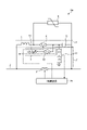
- FIG. 1 is a diagram showing a configuration of a DC circuit breaker 1 according to the first embodiment.
- the DC circuit breaker 1 according to the first embodiment is a mechanical DC circuit breaker (Direct Current Circuit Breaker: DCCB) of a forced arc extinguishing system.
- the DC circuit breaker 1 is provided on the DC line 2 of the power system.
- the left side of the DC line 2 of the DC breaker 1 is connected to a converter (not shown) of a power system that converts AC power into DC power.
- the power system is a power system that performs multi-terminal HVDC power transmission.
- the DC circuit breaker 1 protects the power system by interrupting the DC current in the event of an accident such as a short circuit or a ground fault in the DC line 2.
- the DC breaker 1 cuts off the DC current at the current zero formed by superimposing the resonance current, which is a vibration current, on the DC current flowing through the DC line 2.
- the DC circuit breaker 1 is a control circuit that controls the entire DC circuit breaker 1, the circuit breaker 3, the resonance circuit 4, the lightning arrester 8, the charging circuit 9, the voltage detection circuit 12, and the DC circuit breaker 1. Has 20 and.
- the resonant circuit 4 has a capacitor 5, an on switch 6 as a first switch, and a reactor 7.
- the arrester arrester 8 suppresses overvoltage to a voltage level based on the withstand voltage specification of DCCB.
- the charging circuit 9 is a circuit that charges the capacitor 5 with the DC potential of the DC line 2, and has a charging switch 10 as a second switch and a charging resistor 11.
- the charging resistor 11 is grounded, and the charging switch 10 and the charging resistor 11 are connected in series.
- the voltage detection circuit 12 detects the charging voltage Vc of the capacitor 5.
- the voltage detection circuit 12 is composed of, for example, a voltage dividing circuit having a resistor Z1 and a resistor Z2.
- the resistance Z1 and the resistance Z2 are connected in series, one end of the resistance Z1 is connected to the connection point between the capacitor 5 and the closing switch 6, and one end of the resistance Z2 is grounded.
- the capacitor 5, the on switch 6, and the reactor 7 are connected in series with each other.
- the capacitor 5, the on switch 6, and the reactor 7 are connected in parallel with the cutoff portion 3.
- the lightning arrester 8 is connected in parallel with the capacitor 5 and the on switch 6.
- the cutoff unit 3 is inserted into the DC line 2 and is closed at normal times.
- the cutoff unit 3 cuts off the direct current at the current zero formed by the resonance current and the direct current canceling each other out. That is, the cutoff unit 3 cuts off the direct current by the forced arc extinguishing method.
- the circuit breaker 3 is a circuit breaker capable of high-speed circuit breaker of current, for example, a vacuum circuit breaker (Vacuum Circuit Breaker: VCB).
- the capacitor 5 and the reactor 7 generate a resonance current by discharging the capacitor 5.
- the on-off switch 6 is a switch for turning on for forming a current zero point.
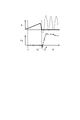
- FIG. 2 is a time chart for explaining the operation of the DC circuit breaker 1 according to the first embodiment.
- the upper figure of FIG. 2 shows the waveform of the current Ie of the cutoff unit 3 at the time of the accident
- the lower figure of FIG. 2 shows the waveform of the voltage Ve of the cutoff unit 3 at the time of the accident.
- the broken line in the upper figure of FIG. 2 shows the waveform of the resonance current.
- the accident current larger than the steady-state current flows through the DC line 2, and the current Ie increases sharply.
- the energizing current in the DC system does not periodically form a current zero, so it is necessary to form a current zero and cut it off by some method.
- the control circuit 20 closes the on switch 6.
- the on-switch 6 When the on-switch 6 is closed, the charge from the capacitor 5 is discharged to the loop including the on-switch 6, the capacitor 5, the reactor 7, and the cutoff portion 3.
- the electric charge is discharged from the capacitor 5, a resonance current that passes through the reactor 7, the cutoff unit 3, and the input switch 6 flows from the capacitor 5.
- the DC circuit breaker 1 superimposes the vibration current in the direction opposite to the direction of the DC current, which is the fault current, on the fault current at the cutoff unit 3 (time t2).
- a current zero is formed by superimposing the oscillating current on the fault current (time t3).
- the control circuit 20 opens the cutoff unit 3 to cut off the current. In this way, the extinguishing of the arc in the cutoff unit 3, that is, the current cutoff is completed.
- the peak value of the resonance current Ig superimposed on the fault current can be calculated by Eq. (1).
- Ig ⁇ (Cp / Lp) ⁇ Vc... (1)
- Cp is the capacitance of the capacitor 5
- Lp is the reactance of the reactor 7
- Vc is the charging voltage of the capacitor 5.
- the lightning arrester 8 starts processing energy from time t4 when the voltage Ve rises to a certain voltage value.
- the lightning arrester 8 processes the energy from the time t4 to the time t5, so that the lightning arrester 8 suppresses the increase of the voltage Ve. In this way, the arrester 8 processes the energy remaining in the power system after the arc is extinguished by the cutoff unit 3.
- the charging voltage Vc of the capacitor 5 is detected by the voltage detection circuit 12.
- the voltage detection circuit 12 outputs the detected charge voltage Vc to the control circuit 20.
- the voltage detection circuit 12 is composed of a voltage divider circuit having resistance Z1 and resistance Z2.
- the voltage detection circuit 12 detects the divided voltage of the resistor Z2 and inputs it to the control circuit 20.
- the control circuit 20 obtains the charging voltage Vc of the capacitor 5 based on the divided voltage of the resistor Z2 and the respective resistance values of the resistors Z1 and Z2.
- the voltage detection circuit 12 may detect the charge voltage Vc by a method other than the voltage dividing circuit.
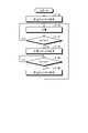
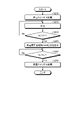
- FIG. 3 is a flowchart showing the charging operation of the control circuit 20.
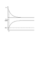
- FIG. 4 is a time chart showing changes over time in the charging voltage Vc of the capacitor 5.
- the control circuit 20 closes the charging switch 10 (step S100).
- the capacitor 5 is charged in the charging path indicated by the arrow F in FIG. 1, and the charging voltage Vc rises (step S105).
- the control circuit 20 monitors the charge voltage Vc obtained from the detection value of the voltage detection circuit 12.
- the control circuit 20 opens the charging switch 10 (step). S120).
- the charging switch 10 is a switch that can cut off the current.
- the first voltage value Vu is, for example, the rated voltage of the module constituting the DC circuit breaker 1 and functions as an upper limit value of the charge voltage control.
- the control circuit 20 closes the charging switch 10 (step S140).
- the second voltage value Vd is a value slightly smaller than the first voltage value Vu by a value ⁇ , and functions as a lower limit value of the charge voltage control.
- step S105 When the charging switch 10 is closed, the capacitor 5 is recharged and the charging voltage Vc rises again (step S105). The operations of steps S105 to S140 are repeated until the operation of the DC circuit breaker 1 is completed. By such control, the control circuit 20 keeps the charging voltage Vc within the range from the second voltage value Vd to the first voltage value Vu.
- the first voltage value Vu is set to 80 kV
- the second voltage value Vd is set to a value slightly smaller than 80 kV by a value ⁇ . ..
- the period from time t0 to t1 shows the natural discharge period due to the stray impedance after the charging of the capacitor 5 is completed.
- the charge switch 10 is open.
- the charging switch 10 is closed.
- the capacitor 5 is recharged and the charging voltage Vc rises again.
- the charging switch 10 is opened. This prevents the capacitor 5 from being discharged via the charging resistor 11.
- the charging switch 10 when the charging voltage Vc becomes larger than the first voltage value Vu, the charging switch 10 is opened, and when the charging voltage Vc becomes smaller than the second voltage value Vd, the charging switch 10 is closed. Therefore, the charging voltage Vc can be kept within the range from the second voltage value Vd to the first voltage value Vu. As a result, the charging resistor 11 can be miniaturized.
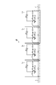
- FIG. 5 is a diagram showing the configuration of the DC circuit breaker system 30 according to the second embodiment.
- the DC circuit breaker system 30 according to the second embodiment is configured by connecting a plurality of DC circuit breakers 1a, 1b, 1c, and 1d in series.
- FIG. 6 is a diagram showing the configuration of the DC circuit breaker 1a according to the second embodiment.
- the other DC circuit breakers 1b, 1c, 1d also have the same configuration as the DC circuit breaker 1a.
- the left side of the DC line 2 is connected to a converter (not shown) that converts an AC system into a DC system.
- a converter (not shown) that converts an AC system into a DC system.
- the DC circuit breaker system 30 by connecting four DC circuit breakers 1a to 1d having a rating of 80 kV in series, it can be applied to a power system of 320 kV. That is, 320 kV of DC power is supplied to the DC line 2 from the converter (not shown).
- each DC circuit breaker 1a includes a circuit breaker 3, a resonance circuit 4 having a capacitor 5, a closing switch 6, and a reactor 7, a lightning arrester 8, a charging switch 10, and a variable resistance for charging 15. It has a charging circuit 9, a voltage detection circuit 12, and a control circuit 25.
- the charging resistor 11 of FIG. 1 is replaced with the charging variable resistor 15, and the control circuit 20 of FIG. 1 is replaced with the control circuit 25.
- the operations and functions of the other components are the same as those shown in FIG. 1, and duplicate description will be omitted.
- the variable resistance 15 for charging changes the resistance value by the control of the control circuit 25. The details will be described later.
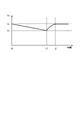
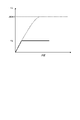
- FIG. 7 is a time chart showing the charging state of the capacitors 5 of the DC circuit breakers 1a to 1d.
- the vertical axis of FIG. 7 is the charging voltage Vc.
- the charging state of the capacitor 5 is shown by a solid line.
- the charging switch 10 is closed, the capacitor 5 is charged and the charging voltage Vc rises.
- the charging voltage Vc reaches the fourth voltage value Vu, which is the rated voltage, the charging switch 10 is opened and charging is stopped. This prevents the capacitor 5 from being overcharged to a system voltage of 320 kV, as shown by the dashed line.
- FIG. 8 is a time chart for explaining the cutoff of the charging current of the capacitor of the DC circuit breaker according to the second embodiment.
- FIG. 8 shows the relationship between the charging voltage Vc and the charging current Ic, and at the time t1 when the charging voltage Vc reaches the rated voltage of 80 kV, the charging current is still in a large current value state.
- the resistance value of the variable charging resistor 15 is increased before the charging is completed, so that the charging current Ic is reduced to a level at which the charging switch 10 can effectively cut off the charging current Ic.
- the charging voltage Vc reaches the third voltage value V1, which is slightly smaller than the fourth voltage value Vu, which is the rated voltage of 80 kV
- the resistance value of the variable charging resistor 15 becomes steady. It can be changed to a second resistance value larger than the first resistance value which is the resistance value. This makes it possible to easily cut off the current of the charging switch 10.
- FIG. 9 is a flowchart showing the charging operation of the control circuit 25 of the second embodiment.
- the control circuit 25 of the DC circuit breaker 1a will be described, but the control circuits 25 of the other DC circuit breakers 1b, 1c, 1d also operate in the same manner.
- the control circuit 25 closes the charging switch 10 (step S200).
- the capacitor 5 is charged in the charging path indicated by the arrow F in FIGS. 5 and 6, and the charging voltage Vc rises (step S205).
- the control circuit 25 monitors the charge voltage Vc obtained from the detection value of the voltage detection circuit 12.
- the control circuit 25 sets the resistance value of the variable charging resistor 15 from the first resistance value which is the steady resistance value.
- the resistance value is changed to a second resistance value larger than the resistance value of 1 (step S220).
- the control circuit 25 opens the charging switch 10 (step S240). ).
- the charging variable resistance 15 reduces the charging current Ic to a level at which the charging switch 10 can easily shut off the charging current Ic. After that, since the charging switch 10 is opened, it is prevented that the capacitor 5 is discharged via the grounded variable charging resistor 15.
- the control circuit 25 closes the charging switch 10 and the charging voltage Vc becomes smaller than the first voltage value Vu.
- the control for opening the charging switch 10 is executed. Therefore, the charging voltage Vc can be kept within the range between the second voltage value Vd and the first voltage value Vu.
- the resistance value of the variable resistance for charging 15 is set in a steady state before the charging of the capacitor 5 is completed. Since the resistance value can be changed to a second resistance value larger than the first resistance value, which is the resistance value of the above, the current cutoff of the charging switch 10 can be facilitated. Further, in the DC circuit breaker system 30 in which a plurality of DC circuit breakers 1a to 1d are connected in series, each DC circuit breaker 1a to 1d is the rated voltage of the module constituting each DC circuit breaker 1a to 1d with respect to the capacitor 5. Since charging is stopped, it is possible to prevent the capacitor 5 from being overcharged to the system voltage.
- FIG. 10 is a diagram showing an example of the hardware configuration of the control circuits 20 and 25 included in the DC circuit breakers 1, 1a to 1d according to the first or second embodiment.
- FIG. 10 shows a hardware configuration when the functions of the control circuits 20 and 25 are realized by using the hardware for executing the program.
- the processor 31, the memory 32, and the interface 33 are connected to each other via a bus.
- the processor 31 is a CPU (Central Processing Unit), a processing device, a computing device, a microprocessor, a microcomputer, or a DSP (Digital Signal Processor). Each function of the control circuits 20 and 25 is realized by the processor 31 and software, firmware, or a combination of software and firmware.
- the software or firmware is described as a program and stored in a memory 32 which is a built-in memory.
- the memory 32 is a non-volatile or volatile semiconductor memory, and is a RAM (Random Access Memory), ROM (Read Only Memory), flash memory, EPROM (Erasable Programmable Read Only Memory) or EEPROM (registered trademark) (Electrically Erasable). Programmable Read Only Memory).
- the interface 33 is responsible for signal input and signal output.
- the interface 33 outputs a command to each of the cutoff unit 3, the on switch 6, and the charge switch 10.
- a signal indicating the detection result of the voltage detection circuit 12 is input to the interface 33.
- the configuration shown in the above-described embodiment shows an example of the contents of the present disclosure, can be combined with another known technique, and is one of the configurations as long as it does not deviate from the gist of the present disclosure. It is also possible to omit or change the part.
Landscapes
- Engineering & Computer Science (AREA)
- Power Engineering (AREA)
- Driving Mechanisms And Operating Circuits Of Arc-Extinguishing High-Tension Switches (AREA)
Abstract
Description
図1は、実施の形態1にかかる直流遮断器1の構成を示す図である。実施の形態1にかかる直流遮断器1は、強制消弧方式の機械式の直流遮断器(Direct Current Circuit Breaker:DCCB)である。直流遮断器1は、電力系統の直流線路2に設けられている。直流遮断器1の直流線路2の図示左側は、交流電力を直流電力に変換する電力系統のコンバータ(図示せず)に接続されている。
Ig=√(Cp/Lp)×Vc …(1)
ここで、Cpはコンデンサ5の静電容量、Lpはリアクトル7のリアクタンス、Vcはコンデンサ5の充電電圧である。LC共振電流の波高値が、遮断する電流値よりも大きくなるように、式(1)の各パラメータを調整する。
図5は、実施の形態2にかかる直流遮断器システム30の構成を示す図である。実施の形態2にかかる直流遮断器システム30は、複数の直流遮断器1a,1b,1c,1dが直列に接続されて構成されている。図6は、実施の形態2にかかる直流遮断器1aの構成を示す図である。他の直流遮断器1b,1c,1dも、直流遮断器1aと同じ構成を有している。
Claims (4)
- 直流線路に挿入され、定常時は閉である遮断部と、
前記遮断部に並列に接続され、互いに直列に接続されているコンデンサ、リアクトルおよび定常時は開である第1のスイッチを有する共振回路と、
前記コンデンサの充電電圧を検出する電圧検出回路と、
接地された充電用抵抗と第2のスイッチとが直列接続され、前記コンデンサを前記直流線路の直流電位で充電する充電回路と、
事故発生時に、前記第1のスイッチを閉にし、前記直流線路に流れる直流電流に前記共振回路により生じる共振電流を重畳して電流零点を形成し、前記遮断部を開として前記直流電流を遮断する制御回路と、
を備え、
前記制御回路は、前記第2のスイッチを閉にして前記コンデンサを充電し、この後、検出された前記充電電圧が第1の電圧値より大きくなると、前記第2のスイッチを開とし、検出された前記充電電圧が前記第1の電圧値より小さな第2の電圧値より小さくなると前記第2のスイッチを閉とする
ことを特徴とする直流遮断器。 - 前記第1の電圧値は、定格電圧であることを特徴とする請求項1に記載の直流遮断器。
- 複数の直流遮断器が直列接続される直流遮断器システムであって、
各直流遮断器は、
直流線路に挿入され、定常時は閉である遮断部と、
前記遮断部に並列に接続され、互いに直列に接続されているコンデンサ、リアクトルおよび定常時は開である第1のスイッチを有する共振回路と、
前記コンデンサの充電電圧を検出する電圧検出回路と、
抵抗値を可変できる接地された充電用可変抵抗と第2のスイッチとが直列接続され、前記コンデンサを前記直流線路の直流電位で充電する充電回路と、
事故発生時に、前記第1のスイッチを閉にし、前記直流線路に流れる直流電流に前記共振回路により生じる共振電流を重畳して電流零点を形成し、前記遮断部を開として前記直流電流を遮断する制御回路と、
をそれぞれ備え、
前記制御回路は、前記第2のスイッチを閉にして前記コンデンサを充電し、この後、検出された前記充電電圧が第3の電圧値になると、前記充電用可変抵抗の抵抗値を定常時の抵抗値である第1の抵抗値より大きな第2の抵抗値に変え、この後、検出された前記充電電圧が前記第3の電圧値より大きな第4の電圧値より大きくなると、前記第2のスイッチを開とする
ことを特徴とする直流遮断器システム。 - 前記第4の電圧値は、前記各直流遮断器の定格電圧であることを特徴とする請求項3に記載の直流遮断器システム。
Priority Applications (4)
| Application Number | Priority Date | Filing Date | Title |
|---|---|---|---|
| JP2021517072A JP6921364B1 (ja) | 2020-12-09 | 2020-12-09 | 直流遮断器および直流遮断器システム |
| EP20965083.7A EP4261865B1 (en) | 2020-12-09 | 2020-12-09 | Dc breaker and dc breaker system |
| US18/247,304 US12243697B2 (en) | 2020-12-09 | 2020-12-09 | Direct-current circuit breaker and direct-current circuit breaker system |
| PCT/JP2020/045906 WO2022123700A1 (ja) | 2020-12-09 | 2020-12-09 | 直流遮断器および直流遮断器システム |
Applications Claiming Priority (1)
| Application Number | Priority Date | Filing Date | Title |
|---|---|---|---|
| PCT/JP2020/045906 WO2022123700A1 (ja) | 2020-12-09 | 2020-12-09 | 直流遮断器および直流遮断器システム |
Publications (1)
| Publication Number | Publication Date |
|---|---|
| WO2022123700A1 true WO2022123700A1 (ja) | 2022-06-16 |
Family
ID=77269602
Family Applications (1)
| Application Number | Title | Priority Date | Filing Date |
|---|---|---|---|
| PCT/JP2020/045906 Ceased WO2022123700A1 (ja) | 2020-12-09 | 2020-12-09 | 直流遮断器および直流遮断器システム |
Country Status (4)
| Country | Link |
|---|---|
| US (1) | US12243697B2 (ja) |
| EP (1) | EP4261865B1 (ja) |
| JP (1) | JP6921364B1 (ja) |
| WO (1) | WO2022123700A1 (ja) |
Cited By (2)
| Publication number | Priority date | Publication date | Assignee | Title |
|---|---|---|---|---|
| EP4506976A1 (en) * | 2023-08-11 | 2025-02-12 | Schneider Electric Industries Sas | Current breaking device for interrupting a high voltage direct current path |
| EP4506977A1 (en) * | 2023-08-11 | 2025-02-12 | Schneider Electric Industries Sas | Current breaking apparatus for high voltage direct current path |
Families Citing this family (4)
| Publication number | Priority date | Publication date | Assignee | Title |
|---|---|---|---|---|
| WO2020039580A1 (ja) * | 2018-08-24 | 2020-02-27 | 三菱電機株式会社 | 直流遮断装置 |
| WO2023047556A1 (ja) * | 2021-09-27 | 2023-03-30 | 三菱電機株式会社 | 直流遮断器 |
| US12437942B2 (en) * | 2022-10-07 | 2025-10-07 | Board Of Supervisors Of Louisiana State University And Agricultural And Mechanical College | Bipolar hybrid circuit breaker for low-voltage DC circuits |
| US12438360B2 (en) * | 2022-10-07 | 2025-10-07 | Board Of Supervisors Of Louisiana State University And Agricultural And Mechanical College | Bipolar hybrid circuit breaker for low-voltage dc circuits |
Citations (3)
| Publication number | Priority date | Publication date | Assignee | Title |
|---|---|---|---|---|
| JPS59169008A (ja) * | 1983-03-16 | 1984-09-22 | 株式会社日立製作所 | 直流しや断器の制御方法 |
| WO2013164874A1 (ja) | 2012-05-01 | 2013-11-07 | 三菱電機株式会社 | 直流遮断器 |
| WO2015166600A1 (ja) * | 2014-05-01 | 2015-11-05 | 三菱電機株式会社 | 直流遮断装置 |
Family Cites Families (9)
| Publication number | Priority date | Publication date | Assignee | Title |
|---|---|---|---|---|
| US4740858A (en) * | 1985-08-06 | 1988-04-26 | Mitsubishi Denki Kabushiki Kaisha | Zero-current arc-suppression dc circuit breaker |
| WO2011141055A1 (en) * | 2010-05-11 | 2011-11-17 | Abb Technology Ag | A high voltage dc breaker apparatus |
| EP2523204B1 (en) * | 2011-05-12 | 2019-09-04 | ABB Schweiz AG | Circuit arrangement and method for interrupting a current flow in a DC current path |
| EP2523205B1 (en) * | 2011-05-12 | 2017-04-26 | ABB Schweiz AG | Circuit and method for interrupting a current flow in a DC current path |
| WO2013131581A1 (de) * | 2012-03-09 | 2013-09-12 | Siemens Aktiengesellschaft | Vorrichtung zum schalten eines gleichstroms in einem pol eines gleichspannungsnetzes |
| US9530588B2 (en) * | 2013-03-27 | 2016-12-27 | Abb Technology Ltd | Circuit breaking arrangement |
| KR20150078491A (ko) * | 2013-12-30 | 2015-07-08 | 주식회사 효성 | 고전압 dc 차단기 |
| WO2020039580A1 (ja) | 2018-08-24 | 2020-02-27 | 三菱電機株式会社 | 直流遮断装置 |
| EP3896714B1 (en) | 2018-12-10 | 2024-03-13 | Mitsubishi Electric Corporation | Direct-current circuit breaker |
-
2020
- 2020-12-09 JP JP2021517072A patent/JP6921364B1/ja active Active
- 2020-12-09 WO PCT/JP2020/045906 patent/WO2022123700A1/ja not_active Ceased
- 2020-12-09 US US18/247,304 patent/US12243697B2/en active Active
- 2020-12-09 EP EP20965083.7A patent/EP4261865B1/en active Active
Patent Citations (3)
| Publication number | Priority date | Publication date | Assignee | Title |
|---|---|---|---|---|
| JPS59169008A (ja) * | 1983-03-16 | 1984-09-22 | 株式会社日立製作所 | 直流しや断器の制御方法 |
| WO2013164874A1 (ja) | 2012-05-01 | 2013-11-07 | 三菱電機株式会社 | 直流遮断器 |
| WO2015166600A1 (ja) * | 2014-05-01 | 2015-11-05 | 三菱電機株式会社 | 直流遮断装置 |
Non-Patent Citations (1)
| Title |
|---|
| See also references of EP4261865A4 |
Cited By (2)
| Publication number | Priority date | Publication date | Assignee | Title |
|---|---|---|---|---|
| EP4506976A1 (en) * | 2023-08-11 | 2025-02-12 | Schneider Electric Industries Sas | Current breaking device for interrupting a high voltage direct current path |
| EP4506977A1 (en) * | 2023-08-11 | 2025-02-12 | Schneider Electric Industries Sas | Current breaking apparatus for high voltage direct current path |
Also Published As
| Publication number | Publication date |
|---|---|
| US20230411091A1 (en) | 2023-12-21 |
| EP4261865A4 (en) | 2024-03-06 |
| EP4261865B1 (en) | 2026-03-25 |
| US12243697B2 (en) | 2025-03-04 |
| JPWO2022123700A1 (ja) | 2022-06-16 |
| EP4261865A1 (en) | 2023-10-18 |
| JP6921364B1 (ja) | 2021-08-18 |
Similar Documents
| Publication | Publication Date | Title |
|---|---|---|
| JP6921364B1 (ja) | 直流遮断器および直流遮断器システム | |
| US9875861B2 (en) | Device and method for switching a direct current | |
| KR101935754B1 (ko) | 과전압 과전류 보호회로 및 이동단말 | |
| KR100871573B1 (ko) | 재충전 배터리용 충전/방전 보호 회로 | |
| CN110299744B (zh) | 一种高压电池簇及其过流保护电路和开关盒 | |
| KR101872869B1 (ko) | 충전된 커패시터와 병렬 lc 회로를 사용한 초고속 dc 차단기 | |
| CN107005045B (zh) | 高压直流电流断路装置 | |
| EP3413330B1 (en) | Direct current circuit breaker | |
| WO2013093066A1 (en) | Hybrid dc circuit breaking device | |
| EP2510598B1 (en) | Electronic protection circuit and protection device | |
| JPWO2019012609A1 (ja) | 直流遮断器 | |
| US4442469A (en) | DC Circuit breaker apparatus | |
| JP3023776B2 (ja) | 遅延回路 | |
| JP6801788B2 (ja) | 電力変換装置、電力システムおよび電力システムの無効電力抑制方法 | |
| JP6155854B2 (ja) | 電池システム | |
| JP7214893B2 (ja) | 直流遮断器 | |
| US11972915B2 (en) | Breaking device | |
| EP4411772B1 (en) | Dc circuit breaker | |
| KR102089141B1 (ko) | 양방향 dc 전류 차단 장치 | |
| WO2018135664A1 (ja) | 直流遮断器および直流遮断器の動作方法 | |
| KR100962497B1 (ko) | 지연회로를 이용한 배터리팩의 2차 보호회로 안정화 장치 | |
| CN113708355A (zh) | 抑制直流滤波电容冲击的电路及装置 | |
| JP5442539B2 (ja) | 遮断装置 | |
| WO2018198552A1 (ja) | 直流遮断装置 | |
| JP2018120857A (ja) | 直流遮断器および直流遮断器の動作方法 |
Legal Events
| Date | Code | Title | Description |
|---|---|---|---|
| ENP | Entry into the national phase |
Ref document number: 2021517072 Country of ref document: JP Kind code of ref document: A |
|
| 121 | Ep: the epo has been informed by wipo that ep was designated in this application |
Ref document number: 20965083 Country of ref document: EP Kind code of ref document: A1 |
|
| NENP | Non-entry into the national phase |
Ref country code: DE |
|
| ENP | Entry into the national phase |
Ref document number: 2020965083 Country of ref document: EP Effective date: 20230710 |
|
| WWG | Wipo information: grant in national office |
Ref document number: 18247304 Country of ref document: US |
|
| WWG | Wipo information: grant in national office |
Ref document number: 2020965083 Country of ref document: EP |