WO2022130685A1 - 画像形成装置 - Google Patents
画像形成装置 Download PDFInfo
- Publication number
- WO2022130685A1 WO2022130685A1 PCT/JP2021/029532 JP2021029532W WO2022130685A1 WO 2022130685 A1 WO2022130685 A1 WO 2022130685A1 JP 2021029532 W JP2021029532 W JP 2021029532W WO 2022130685 A1 WO2022130685 A1 WO 2022130685A1
- Authority
- WO
- WIPO (PCT)
- Prior art keywords
- light emitting
- electrodes
- image
- light
- image data
- Prior art date
- Legal status (The legal status is an assumption and is not a legal conclusion. Google has not performed a legal analysis and makes no representation as to the accuracy of the status listed.)
- Ceased
Links
Images






Classifications
-
- G—PHYSICS
- G03—PHOTOGRAPHY; CINEMATOGRAPHY; ANALOGOUS TECHNIQUES USING WAVES OTHER THAN OPTICAL WAVES; ELECTROGRAPHY; HOLOGRAPHY
- G03G—ELECTROGRAPHY; ELECTROPHOTOGRAPHY; MAGNETOGRAPHY
- G03G15/00—Apparatus for electrographic processes using a charge pattern
- G03G15/04—Apparatus for electrographic processes using a charge pattern for exposing, i.e. imagewise exposure by optically projecting the original image on a photoconductive recording material
- G03G15/043—Apparatus for electrographic processes using a charge pattern for exposing, i.e. imagewise exposure by optically projecting the original image on a photoconductive recording material with means for controlling illumination or exposure
-
- H—ELECTRICITY
- H04—ELECTRIC COMMUNICATION TECHNIQUE
- H04N—PICTORIAL COMMUNICATION, e.g. TELEVISION
- H04N1/00—Scanning, transmission or reproduction of documents or the like, e.g. facsimile transmission; Details thereof
- H04N1/024—Details of scanning heads ; Means for illuminating the original
- H04N1/02418—Details of scanning heads ; Means for illuminating the original for picture information pick up and reproduction
-
- H—ELECTRICITY
- H04—ELECTRIC COMMUNICATION TECHNIQUE
- H04N—PICTORIAL COMMUNICATION, e.g. TELEVISION
- H04N1/00—Scanning, transmission or reproduction of documents or the like, e.g. facsimile transmission; Details thereof
- H04N1/024—Details of scanning heads ; Means for illuminating the original
- H04N1/032—Details of scanning heads ; Means for illuminating the original for picture information reproduction
- H04N1/036—Details of scanning heads ; Means for illuminating the original for picture information reproduction for optical reproduction
-
- H—ELECTRICITY
- H04—ELECTRIC COMMUNICATION TECHNIQUE
- H04N—PICTORIAL COMMUNICATION, e.g. TELEVISION
- H04N1/00—Scanning, transmission or reproduction of documents or the like, e.g. facsimile transmission; Details thereof
- H04N1/04—Scanning arrangements, i.e. arrangements for the displacement of active reading or reproducing elements relative to the original or reproducing medium, or vice versa
- H04N1/06—Scanning arrangements, i.e. arrangements for the displacement of active reading or reproducing elements relative to the original or reproducing medium, or vice versa using cylindrical picture-bearing surfaces, i.e. scanning a main-scanning line substantially perpendicular to the axis and lying in a curved cylindrical surface
-
- H—ELECTRICITY
- H04—ELECTRIC COMMUNICATION TECHNIQUE
- H04N—PICTORIAL COMMUNICATION, e.g. TELEVISION
- H04N1/00—Scanning, transmission or reproduction of documents or the like, e.g. facsimile transmission; Details thereof
- H04N1/23—Reproducing arrangements
- H04N1/29—Reproducing arrangements involving production of an electrostatic intermediate picture
-
- G—PHYSICS
- G03—PHOTOGRAPHY; CINEMATOGRAPHY; ANALOGOUS TECHNIQUES USING WAVES OTHER THAN OPTICAL WAVES; ELECTROGRAPHY; HOLOGRAPHY
- G03G—ELECTROGRAPHY; ELECTROPHOTOGRAPHY; MAGNETOGRAPHY
- G03G2215/00—Apparatus for electrophotographic processes
- G03G2215/04—Arrangements for exposing and producing an image
- G03G2215/0402—Exposure devices
- G03G2215/0407—Light-emitting array or panel
-
- H—ELECTRICITY
- H04—ELECTRIC COMMUNICATION TECHNIQUE
- H04N—PICTORIAL COMMUNICATION, e.g. TELEVISION
- H04N1/00—Scanning, transmission or reproduction of documents or the like, e.g. facsimile transmission; Details thereof
- H04N1/04—Scanning arrangements, i.e. arrangements for the displacement of active reading or reproducing elements relative to the original or reproducing medium, or vice versa
- H04N1/19—Scanning arrangements, i.e. arrangements for the displacement of active reading or reproducing elements relative to the original or reproducing medium, or vice versa using multi-element arrays
- H04N1/195—Scanning arrangements, i.e. arrangements for the displacement of active reading or reproducing elements relative to the original or reproducing medium, or vice versa using multi-element arrays the array comprising a two-dimensional [2D] array
Definitions
- the present invention relates to an image forming apparatus such as an electrophotographic copying machine and an electrophotographic printer that forms an image on a sheet by using an electrophotographic image forming method.
- an electrostatic latent image is formed on the surface of the photoconductor by irradiating the surface of the photoconductor with light corresponding to the image data.
- toner is adhered to the electrostatic latent image on the surface of the photoconductor by a developing device to form a toner image, the toner image is transferred to a sheet, and the toner image transferred to the sheet is heated by a fixing device to form a sheet. It is fixed to form an image.
- a light emitting unit using an organic EL and light emitted from the light emitting unit are used as a device for the photoconductor.
- An image forming apparatus including an exposure head having a lens for forming an image on the surface is described.
- Japanese Patent Application Laid-Open No. 2018-134820 describes a configuration in which a plurality of light emitting portions irradiate the same portion of the surface of the photoconductor with light in order to supplement the amount of light for forming an electrostatic latent image on the surface of the photoconductor. Specifically, in the exposure head, the light emitting portions are two-dimensionally arranged in the rotation axis direction (main scanning direction) and the rotation direction (sub-scanning direction) of the photoconductor.
- the same portion on the surface of the photoconductor is irradiated from the plurality of light emitting portions.
- irradiating the same portion of the surface of the photoconductor from a plurality of light emitting portions with light in this way is referred to as multiple exposure.
- the exposure head if the mounting position is displaced when the light emitting portion is mounted on the substrate, the exposure position on the photoconductor may be displaced and the position of the image may be displaced.
- dithering processing is performed with image data having a higher resolution than the interval in the main scanning direction of the light emitting portion, and the image data is shifted according to the amount of deviation of the mounting position of the light emitting portion.
- a configuration for converting image data according to the pitch in the main scanning direction of the light emitting unit is described. As a result, the misalignment of the image can be corrected with a resolution higher than the pitch in the main scanning direction of the light emitting portion.
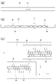
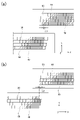
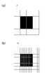
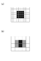
- FIG. 18A shows the image data when the image data is subjected to the dithering process with the image data having a resolution higher than the pitch in the main scanning direction of the light emitting unit and the image data is shifted according to the amount of deviation of the mounting position of the light emitting unit. It is a figure which shows an example.
- FIG. 18B is a diagram when the image data shown in FIG. 18A is converted according to the pitch in the main scanning direction of the light emitting unit.
- FIG. 18 in the configuration of Japanese Patent Application Laid-Open No. 2019-217653, when the high-resolution image data is converted according to the pitch in the main scanning direction of the light emitting portion, the data at the edge portion of the image becomes an intermediate value. The sharpness of the image may decrease.
- An object of the present invention is to secure the amount of light by multiple exposure in the exposure head, suppress the decrease in sharpness of the image, and correct the image position with a resolution higher than the pitch in the main scanning direction of the light emitting portion. It is to provide an image forming apparatus capable.
- a typical configuration of the present invention is an image forming apparatus that irradiates the surface of a photoconductor with light to form an electrostatic latent image and attaches toner to the electrostatic latent image to form an image. It is an exposure head that irradiates the surface of the surface with light to form the electrostatic latent image, and is a substrate and a plurality of electrodes two-dimensionally arranged in the rotation direction of the photoconductor and the rotation axis direction of the photoconductor.
- a first electrode layer including a plurality of electrodes separately arranged on the substrate, a light emitting layer laminated on the first electrode layer and emitting light when a voltage is applied, and the light emitting layer with respect to the light emitting layer.
- An exposure head having a light emitting portion which is arranged on the side opposite to the side where the first electrode layer is arranged and includes a second electrode layer capable of transmitting light, and image data so that the light emitting layer emits light. Based on this, it is a control unit that controls the application of voltage to each of the plurality of electrodes included in the first electrode layer, and controls the voltage to a plurality of electrodes in which one pixel is arranged at different positions in the rotation direction.
- a control unit capable of controlling a voltage to each of the plurality of electrodes based on the image data is provided, and the plurality of electrodes for forming the same pixel are rotated.
- the electrodes are arranged so that a part of the electrodes overlap each other when viewed from a direction, and the distances between the centers of gravity of the plurality of electrodes are evenly spaced in the rotation axis direction.
- the width of the electrodes in the rotation axis direction is W1 [mm]
- the number of the plurality of electrodes for forming the same pixel is n
- the distance between the equidistant centers of gravity in the rotation axis direction is d3 [mm].
- d3 W1 / n (n is a natural number of 2 or more)
- the plurality of electrodes for forming the same pixel are located with the center of gravity of each electrode at an interval of the d3 in the direction of the rotation axis.
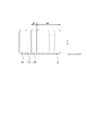
- FIG. 1 is a schematic cross-sectional view of an image forming apparatus.
- 2 (a) and 2 (b) are perspective views and cross-sectional views of the photosensitive drum and the exposure head.
- 3 (a) to 3 (c) are views showing the mounting surface of the printed circuit board included in the exposure head.
- 4 (a) and 4 (b) are diagrams showing the positional relationship between the two light emitting element array chips and the light emitting unit used.
- FIG. 5 is a schematic diagram of a light emitting element array chip.
- FIG. 6 is a cross-sectional view of a light emitting element array chip.
- FIG. 7 is a schematic diagram for explaining the arrangement of the light emitting unit.
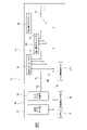
- FIG. 8 is a block diagram showing a system configuration of an image controller unit and an exposure head.
- 9 (a) and 9 (b) are diagrams showing examples of image data before and after high-resolution processing.
- FIG. 10 is a block diagram showing a system configuration of a light emitting element array chip.
- FIG. 11 is a circuit diagram of the data holding unit.
- FIG. 12 is an operation timing chart of the data holding unit.
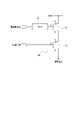
- FIG. 13 is a circuit diagram of the analog section.
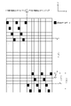
- FIG. 14 is a diagram showing image data sent to the light emitting unit of the light emitting element array chip.
- FIG. 15 is a schematic diagram showing the position of light on the photosensitive drum when the light emitting unit emits light.
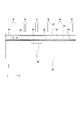
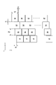
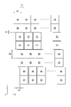
- FIG. 16 is a schematic diagram for explaining the arrangement of the light emitting unit.
- FIG. 17 is a schematic diagram for explaining the arrangement of the light emitting unit.
- 18 (a) and 18 (b) are explanatory views for explaining a conventional configuration.
- the image forming apparatus A is a full-color image forming apparatus that forms an image by transferring four color toners of yellow Y, magenta M, cyan C, and black K to a sheet.
- Y, M, C, and K are added as subscripts to the members that use the toner of each color, except that the composition and operation of each member are different in the color of the toner used. Since they are substantially the same, the subscripts are omitted as appropriate unless a distinction is required.
- FIG. 1 is a schematic cross-sectional view of the image forming apparatus A.
- the image forming apparatus A has an image forming portion for forming an image.
- the image forming unit includes a photosensitive drum 1 (1Y, 1M, 1C, 10K) as a photoconductor, a charging device 2 (2Y, 2M, 2C, 2K), an exposure head 6 (6Y, 6M, 6C, 6K), and a developing device. It has 4 (4Y, 4M, 4C, 4K) and a transfer device 5 (5Y, 5M, 5C, 5K).
- the sheet S housed in the sheet cassette 99a or the sheet cassette 99b is sent to the resist roller 96 by the pickup rollers 91a, 91b, the feeding rollers 92a, 92b, and the transport rollers 93a to 93c. After that, the sheet S is fed to the transport belt 11 by the resist roller 96 at a predetermined timing.
- the surface of the photosensitive drum 1Y is first charged by the charging device 2Y.
- the exposure head 6Y irradiates the surface of the photosensitive drum 10Y with light according to the image data read by the image reading unit 90 or the image data transmitted from an external device (not shown), and the surface of the photosensitive drum 10Y is static.
- Form an electro-latent image After that, the yellow toner is attached to the electrostatic latent image formed on the surface of the photosensitive drum 1Y by the developing device 4Y, and the yellow toner image is formed on the surface of the photosensitive drum 1Y.
- the toner image formed on the surface of the photosensitive drum 1Y is transferred to the sheet S conveyed by the transfer belt 11 by applying a transfer bias to the transfer device 5Y.
- the photosensitive drums 1M, 1C, and 1K are also irradiated with light from the exposure heads 6M, 6C, and 6K to form an electrostatic latent image, and magenta, cyan, and black are formed by the developing devices 4M, 4C, and 4K.
- a toner image is formed.
- these toner images are transferred superimposed on the yellow toner image on the sheet S.
- a full-color toner image corresponding to the image data is formed on the surface of the sheet S.
- the sheet S carrying the toner image is conveyed to the fixing device 94 by the conveying belt 97, and is heated and pressurized in the fixing device 94. As a result, the toner image on the sheet S is fixed to the sheet S. After that, the sheet S on which the toner image is fixed is discharged to the discharge tray 95 by the discharge roller 98.
- FIG. 2A is a perspective view of the photosensitive drum 1 and the exposure head 6.
- FIG. 2B is a cross-sectional view of the photosensitive drum 1 and the exposure head 6.
- 3A and 3B are views showing the mounting surfaces of the printed circuit board 22 included in the exposure head 6 on one side and the other side.
- FIG. 3 (c) is an enlarged view of the region V shown in FIG. 3 (b).
- the exposure head 6 is fixed at a position facing the surface of the photosensitive drum 1 by a fixing member (not shown).
- the exposure head 6 has a light emitting element array chip 40 that emits light and a printed circuit board 22 on which the light emitting element array chip 40 is mounted. Further, it has a rod lens array 23 that forms (condenses) the light emitted from the light emitting element array chip 40 on the photosensitive drum 1, and a housing 24 to which the rod lens array 23 and the printed circuit board 22 are fixed.
- the connector 21 is mounted on the surface of the printed circuit board 22 opposite to the mounting surface of the light emitting element array chip 40.
- the connector 21 is provided for transmitting a control signal of the light emitting element array chip 40 transmitted from the image controller unit 70 (FIG. 8) and for connecting a power supply line.
- the light emitting element array chip 40 is driven via the connector 21.
- 20 light emitting element array chips 40 are mounted in two rows arranged in a staggered pattern on the printed circuit board 22. Further, in each light emitting element array chip 40, 748 light emitting units 50 are arranged in the longitudinal direction (arrow X direction) at a predetermined resolution pitch. Further, in each light emitting element array chip 40, four light emitting units 50 are arranged at a predetermined pitch in the lateral direction (arrow Y direction). That is, in each light emitting element array chip 40, the light emitting units 50 are two-dimensionally arranged in the arrow X direction and the arrow Y direction. The four light emitting units 50 arranged in the Y direction of the arrow form the same pixel by multiple exposure described later.
- the resolution pitch of the light emitting element array chip 40 is 1200 dpi (about 21.16 ⁇ m). Further, the distance from one end to the other end of the light emitting portion 50 of each light emitting element array chip 40 in the longitudinal direction is about 15.828 mm. That is, the exposure head 6 includes a total of 14960 light emitting units 50 in the X direction of the arrow, which enables exposure processing corresponding to an image width in the longitudinal direction of about 316 mm ( ⁇ 15.8 mm ⁇ 20 chips). It has become.
- the distance L1 between the light emitting portions 50 of the adjacent light emitting element array chips 40 is about 105 ⁇ m (5 pixels at 1200 dpi and 10 pixels at 2400 dpi). It has become.
- the light emitting element array chips 40 adjacent to each other in the Y direction of the arrow are arranged so that the light emitting portions 50 of each of them overlap in the X direction of the arrow.
- the reason for this is that the position shift occurs in the mounting process of the light emitting element array chip 40, the position of the light irradiated on the photosensitive drum 1 shifts at the boundary portion of each light emitting element array chip 40, and the image streaks occur. This is to prevent the formation of.
- the overlap amount is calculated from the maximum amount of mounting variation of the mounting device (die bonder), and is set to an amount at which no gap is formed between the light emitting portions 50 of the light emitting element array chips 40 adjacent to each other in the arrow Y direction.
- the amount of misalignment at the time of mounting the light emitting element array chip 40 is measured and stored in the manufacturing process.
- the image controller unit 70 selectively selects the light emitting unit 50 as described below based on the position shift information of the light emitting element array chip 40 stored in the head information storage unit 171 at the time of image formation. Light is emitted to suppress the occurrence of image streaks.
- FIG. 4 is a diagram showing two light emitting element array chips 40 adjacent to each other in the Y direction of the arrow.
- the light emitting unit 50 with diagonal lines indicates the light emitting unit 50 used at the time of exposure
- the light emitting unit 50 without diagonal lines indicates the light emitting unit 50 not used at the time of exposure.
- the relative positions of the two light emitting element array chips 40 adjacent to each other in the Y direction of the arrow are different in the X direction of the arrow.
- the distance L2 between the light emitting units 50 of the two light emitting element array chips 40 adjacent to each other in the Y direction of the arrow and the X direction of the light emitting unit 50 used at the time of exposure is set.
- the light emitting unit 50 to be used at the time of exposure is selected so as to be closest to the interval of 4800 dpi.
- the distance L2 is set to be close to the interval of 4800 dpi, but the distance L2 is the exposure head 6. It is set according to the exposure resolution in the X direction of the arrow.
- the arrow X direction which is the longitudinal direction of the light emitting element array chip 40, is the rotation axis direction of the photosensitive drum 1, and is also the main scanning direction.
- the arrow Y direction which is the lateral direction of the light emitting element array chip 40, is the rotation direction of the photosensitive drum 1, and is also the sub-scanning direction.
- the rotation direction of the photosensitive drum 1 is the tangential direction of the photosensitive drum 1 at the exposure position on the photosensitive drum 1 where the light is collected by the exposure head 6.
- the arrow Z direction is a stacking direction in which each layer of the light emitting portion 50 of the layer structure described later overlaps.
- the longitudinal direction of the light emitting element array chip 40 may be tilted by about ⁇ 1 ° with respect to the rotation axis direction of the photosensitive drum 1. Further, the lateral direction of the light emitting element array chip 40 may also be tilted by about ⁇ 1 ° with respect to the rotation direction of the photosensitive drum 1.
- FIG. 5 is a schematic diagram of the light emitting element array chip 40.
- FIG. 6 is a cross-sectional view of the light emitting element array chip 40 cut along the MM cross section shown in FIG.
- FIG. 7 is a schematic diagram for explaining the arrangement of the light emitting unit 50 of the light emitting element array chip 40.
- a light emitting board 42 (board) incorporating a circuit unit 46 for controlling the light emitting unit 50 and a plurality of light emitting units 50 are regularly placed on the light emitting board 42. It has an arranged light emitting region 44 and a wire bonding pad 48. The signal input / output between the outside of the light emitting element array chip 40 and the circuit unit 46 and the power supply to the circuit unit 46 are performed through the wire bonding pad 48.
- the circuit unit 46 can use a circuit including an analog drive circuit, a digital control circuit, or both.
- a plurality of light emitting units 50 are two-dimensionally arranged on the light emitting substrate 42 and the light emitting substrate 42 at regular intervals (intervals d1 and d2 shown in FIG. 7) in the arrow X direction and the arrow Y direction. It is composed of a lower electrode 54, a light emitting layer 56, and an upper electrode 58.
- the lower electrode 54 (first electrode layer having a plurality of electrodes) is a plurality of electrodes formed on the light emitting substrate 42 in a layered manner and separately, and is an electrode provided corresponding to each pixel. be. That is, each lower electrode 54 is provided to form one pixel.
- the upper electrode 58 (second electrode layer) is laminated on the light emitting layer 56 at a position opposite to the side where the lower electrode 54 is arranged with respect to the light emitting layer 56.
- the upper electrode 58 is an electrode capable of transmitting (transmitting) light having a emission wavelength of the light emitting layer 56.
- the circuit unit 46 controls the potential of the selected lower electrode 54 based on the control signal generated according to the image data, and causes a potential difference between the selected lower electrode 54 and the upper electrode 58.
- a potential difference occurs between the upper electrode 58, which is the anode, and the lower electrode 54, which is the cathode, electrons flow from the cathode into the light emitting layer 56, and holes flow from the anode into the light emitting layer 56.
- the light emitting layer 56 emits light by recombining electrons and holes in the light emitting layer 56.
- the light emitted from the light emitting layer 56 toward the upper electrode 58 is transmitted through the upper electrode 58 and emitted. Further, the light directed from the light emitting layer 56 toward the lower electrode 54 is reflected from the lower electrode 54 toward the upper electrode 58, and the reflected light is also transmitted through the upper electrode 58 and emitted. In this way, the light emitting unit 50 emits light. Although there is a time difference in the emission timing between the light emitted directly from the light emitting layer 56 toward the upper electrode 58 and the light reflected from the lower electrode 54 and emitted from the upper electrode 58, the light emitting unit 50 Since the layers are extremely thin, they can be regarded as almost simultaneous.
- the light emitting substrate 42 is a silicon substrate.
- the upper electrode 58 is preferably transparent with respect to the emission wavelength of the light emitting layer 56.
- a transparent electrode such as indium tin oxide (ITO)
- ITO indium tin oxide
- the aperture ratio becomes substantially 100%, and the light emitted by the light emitting layer 56 is emitted as it is through the upper electrode 58.
- the upper electrode 58 is an anode commonly provided for each lower electrode 54, but even if the upper electrode 58 is individually provided for each of the lower electrodes 54, each of the plurality of lower electrodes 54 is provided. There may be a configuration in which one upper electrode 58 is provided on the surface.
- the entire body does not necessarily have to be a transparent electrode, and only the opening that emits light is a transparent electrode, and the other than the opening is wired with an electrode other than the transparent electrode such as a metal electric wire. May be good.
- the light emitting layer 56 an organic EL film, an inorganic EL layer, or the like is used.
- the light emitting layer 56 includes functional layers such as an electron transport layer, a hole transport layer, an electron injection layer, a hole injection layer, an electron block layer, and a hole block layer as needed. It may be a laminated structure including. Further, the light emitting layer 56 may be continuously formed in the direction of the arrow X, or may be divided into the same size as the lower electrode 54. Further, each lower electrode 54 may be divided into a plurality of groups, and one light emitting layer 56 may be laminated on the upper part of the lower electrode 54 belonging to the group for each divided group.
- a light-emitting material such as an organic EL layer or an inorganic EL layer that is sensitive to water
- a sealing method for example, a thin film such as an oxide of silicon, a nitride of silicon, or an oxide of aluminum is formed as a simple substance or a laminated sealing film.
- a method for forming the sealing film a method excellent in covering performance of a structure such as a step is preferable, and for example, an atomic layer deposition method (ALD method) or the like can be used.
- ALD method atomic layer deposition method
- the material, composition, forming method, etc. of the sealing film are examples, and the present invention is not limited to the above-mentioned examples, and a suitable one may be appropriately selected.
- the lower electrode 54 is preferably made of a metal having a high reflectance with respect to the emission wavelength of the light emitting layer 56.
- a metal having a high reflectance For example, Ag, Al, or an alloy of Ag and Al is used.
- the lower electrode 54 is formed by using the Si integrated circuit processing technique together with the formation of the circuit portion 46, and is directly connected to the drive portion of the circuit portion 46.
- the process rule becomes highly accurate at about 0.2 ⁇ m, so that the lower electrode 54 can be arranged with high accuracy and high density.
- the lower electrode 54 can be arranged at a high density, most of the light emitting region 44 can be made to emit light, and the utilization efficiency of the light emitting region 44 can be improved.
- the organic material of the light emitting layer 56 is filled between the lower electrodes 54, and each lower electrode 54 is partitioned by the organic material.
- the light emitting unit 50 when the voltage applied across the ends exceeds a predetermined value, a current starts to flow, and after that, the value of the current increases almost in proportion to the value of the voltage.
- the voltage at which the current begins to flow in each light emitting unit 50 There are variations in the voltage at which the current begins to flow in each light emitting unit 50. Therefore, at the stage before the product is shipped from the factory, the light emitting units 50 of the light emitting element array chip 40 are individually and sequentially emitted, and the light emitting unit 50 so that the light collected through the rod lens array 23 has a predetermined amount of light. The current flowing through is adjusted.
- the exposure head 6 not only adjusts the amount of light described above, but also adjusts the focus to adjust the distance between the light emitting element array chip 40 and the rod lens array 23 at the stage before the product is shipped from the factory.
- the light emitting units 50 are arranged in a matrix in the light emitting region 44 at predetermined intervals in the arrow X direction and the arrow Y direction.
- the width W1 of the light emitting unit 50 in the arrow X direction is 19.80 ⁇ m
- the distance d1 between the light emitting units 50 adjacent to each other in the arrow X direction is 0.68 ⁇ m. That is, the light emitting units 50 are arranged at a pitch of 21.16 ⁇ m (1200 dpi) in the X direction of the arrow.
- the pitch of the light emitting unit 50 in the arrow X direction may be deviated within the range of the tolerance.
- the tolerance of the pitch of the light emitting unit 50 in the arrow X direction is ⁇ 1% with respect to the pitch of the light emitting unit 50 in the arrow X direction in the design designation. That is, the tolerance of the pitch of the light emitting unit 50 of the present embodiment in the arrow X direction is ⁇ 0.21 ⁇ m.
- the width W2 of the light emitting unit 50 in the arrow Y direction is 19.80 ⁇ m as well as the width W1. That is, the light emitting unit 50 of the present embodiment has a square shape with a side of 19.80 ⁇ m. Although the light emitting unit 50 has a square shape because the width W1 and the width W2 are equal, the dimensions of the widths W1 and W2 may deviate within the range of the tolerance. In this embodiment, the tolerances of the widths W1 and W2 are both ⁇ 0.2 ⁇ m.
- the distance d2 between the light emitting units 50 adjacent to each other in the arrow Y direction is also 0.68 ⁇ m as in the space d1, and the light emitting units 50 are arranged at a pitch of 21.16 ⁇ m (1200 dpi) also in the arrow Y direction.
- the pitch of the light emitting unit 50 in the arrow Y direction may be deviated within the range of the tolerance.
- the tolerance of the pitch of the light emitting unit 50 in the arrow Y direction is ⁇ 1% with respect to the pitch of the light emitting unit 50 in the arrow Y direction in the design designation. That is, the tolerance of the pitch of the light emitting unit 50 of the present embodiment in the arrow Y direction is ⁇ 0.21 ⁇ m.
- the distances d1 and d2 of the light emitting unit 50 are set wider than the distance dz (FIG. 6) between the upper electrode 58 and the lower electrode 54. With such a configuration, it is possible to suppress the leakage current between the lower electrodes 54 adjacent to each other in the arrow X direction and the arrow Y direction, and it is possible to suppress the erroneous light emission of the light emitting unit 50.
- the width, shape, arrangement, etc. of the light emitting portion 50 are substantially determined by the width, shape, and arrangement of the lower electrode 54 in the present embodiment, it can be paraphrased as the width, shape, and arrangement of the lower electrode 54.
- the distance between the light emitting portions 50 that is, the distance between the lower electrodes 54 means the distance between the centers of gravity defined based on the position of the center of gravity of the lower electrodes 54 in the design designation.
- the light emitting units 50 adjacent to each other in the Y direction of the arrow are arranged so that their positions are offset by d3 in the X direction of the arrow.
- the interval d3 is set to 5.29 ⁇ m (4800 dpi).
- the positions of the four light emitting units 50 parallel to each other in the Y direction of the arrow are arranged so as to be offset from each other in the X direction of the arrow by an integral multiple of the interval d3.
- the four lower electrodes 54 provided in the Y direction of the arrow to form the same pixel are partially overlapped with each other when viewed from the Y direction of the arrow, and the lower electrodes 54 are provided in the X direction of the arrow. They are arranged so that the distance between the centers of gravity is evenly spaced.
- the interval d3 is determined as follows in this embodiment. That is, the resolution of the image formed by the image forming apparatus A in the main scanning direction (arrow X direction) is m [dpi], the number of light emitting units 50 parallel to the arrow Y direction is n [pieces], and the number of light emitting portions 50 is parallel to the arrow Y direction.
- the reference value of the amount of deviation of the position of the light emitting unit 50 in the arrow X direction is set to the interval d3 [mm] (reference value).
- the interval d3 is determined as follows, the result is the same as the above calculation result of the interval d3. That is, the pitch of the plurality of light emitting units 50 having the same position in the arrow Y direction in the arrow X direction is q [mm], the number of light emitting units 50 parallel to the arrow Y direction is n [pieces], and the light emission is parallel to the arrow Y direction.
- the reference value of the amount of deviation of the position of the portion 50 in the arrow X direction is defined as the interval d3 [mm] (reference value).
- the light emitting units 50 arranged at different positions in the arrow Y direction to form the same pixel are arranged so that the positions of the centers of gravity of the respective light emitting units 50 are located at intervals of d3 in the arrow X direction.
- each light emitting unit has a distance between the centers of gravity of the four light emitting units 50 arranged at different positions in the arrow Y direction at different positions in the arrow X direction to form the same pixel by multiple exposure described later as d3.
- the shape of the light emitting unit 50 is not limited to a square, and the image quality of the output image satisfies the design specifications of the image forming apparatus A by emitting light having an exposure region size corresponding to the output resolution of the image forming apparatus A. If it is, it may be a polygon, a circle, an ellipse, or the like, which is larger than a quadrangle. However, since the organic light emitting material has a smaller amount of light than the LED, the amount of light that changes the potential of the photosensitive drum 1 is increased by making the light emitting unit 50 a square and reducing the distance between the light emitting unit 50 and the adjacent light emitting unit 50.
- the number of light emitting units 50 arranged in parallel in the Y direction of the arrow is not limited to four if two or more are provided, and the amount of light required for the exposure process of the exposure head 6 and the image formed by the image forming apparatus A. It is determined based on the resolution and so on.
- the distance between the light emitting portions 50 that is, the distance between the lower electrodes 54 is defined based on the position of the center of gravity of the lower electrodes 54 on the design name. That is, if the shape of the lower electrode 54 is a regular polygon, the intersection of the diagonal lines, if it is a perfect circle, the center of the circle, and if it is an ellipse, the intersection of the major axis and the minor axis is used as a reference. Distance is set. When the shape of the lower electrode 54 is a regular polygon, the angle may not be a perfect angle and may be R.
- the image controller unit 70 is provided on the main body side of the image forming apparatus A.
- the control performed when processing one image data will be described, but when performing the image forming operation, the same processing is performed for the four image data corresponding to yellow, magenta, cyan, and black. Shall be processed in parallel.
- FIG. 8 is a block diagram showing a system configuration of the image controller unit 70 and the exposure head 6.
- the image controller unit 70 includes an image data generation unit 71, a chip data conversion unit 72, a CPU 73, and a synchronization signal generation unit 74.
- the image controller unit 70 performs image data processing and image formation timing processing by these portions, and transmits a control signal for controlling the exposure head 6 to the printed circuit board 22 of the exposure head 6.
- the image data of the original read by the image reading unit 90 and the image data transferred from the external device via the network are input to the image data generation unit 71 (image processing unit).
- the image data generation unit 71 performs dithering processing on the input image data at the resolution specified by the CPU 73, and generates image data for outputting the image.
- the image data generation unit 71 performs dithering processing with a resolution of 1200 dpi and a binary number of gradations, and then undergoes resolution processing to increase the resolution to 4800 dpi in the main scanning direction, 2400 dpi in the sub-scanning direction, and the number of gradations. Generates binary data. In the high resolution process, 1200 dpi data is simply copied.
- FIG. 9A is a diagram showing an example of image data D1 (first image data) before high resolution processing of the image data generation unit 71.
- FIG. 9B is a diagram showing image data D2 (second image data) obtained by processing the image data D1 to a higher resolution by the image data generation unit 71.
- the image data D2 is generated according to the resolution of the exposure by the light emitting element array chip 40 by the high resolution processing.
- the image data generation unit 71 can generate a binarized data to enable high-definition image formation without losing the sharpness of the image.
- the image data after the dithering process is generated in units of the four light emitting units 50 parallel to each other in the arrow X direction on the photosensitive drum 1. Generated. Of the four rows of light emitting units 50 extending in the X direction of the arrow and parallel to each other in the Y direction of the arrow, the rows of the light emitting unit 50 in the first row and the light emitting unit 50 in the second row have a distance from the center of the rod lens array 23. Since they are different from each other, there is a difference in the amount of light emitted from each row to the photosensitive drum 1.
- the synchronization signal generation unit 74 periodically generates a line synchronization signal (control signal) indicating the start of image data acquisition, and transmits the line synchronization signal (control signal) to the chip data conversion unit 72.
- the CPU 73 has one line of a cycle in which the surface of the photosensitive drum 1 moves in the rotation direction by the pixel size according to the resolution in the sub-scanning direction of the image formed by the image forming apparatus A with respect to the rotation speed of the photosensitive drum 1 set in advance. The period is set, and the synchronization signal generation unit 74 is instructed to time interval of the signal cycle.
- the resolution in the sub-scanning direction of the image formed by the image forming apparatus A is 2400 dpi
- the photosensitive drum 1 rotates at 200 mm / s. Therefore, the time for the photosensitive drum 1 to move by a distance (10.58um) of a pixel size of 2400 dpi is 52.92us, and the period of the line synchronization signal is 52.92us.
- the rotation speed of the photosensitive drum 1 is calculated by the CPU 73 based on a set value stored in a storage unit (not shown).
- the chip data conversion unit 72 synchronizes with the line synchronization signal generated and input by the synchronization signal generation unit 74, and displays image data for one line ⁇ 4 columns (the number of light emitting units 50 in the arrow Y direction). It is divided into light emitting element array chips 40. Then, the chip data conversion unit 72 transmits image data together with the clock signal and the line synchronization signal to each light emitting element array chip 40 via the line synchronization signal line 75, the clock signal line 76, and the image data signal line 77. It should be noted that four image data signal lines 77 are provided, which is the same number as the number of light emitting units 50 in the arrow Y direction.
- the head information storage unit 171 included in the exposure head 6 is connected to the CPU 73 via a communication signal line 79.
- the head information storage unit 171 stores the light emission amount and the mounting position information of each light emitting element array chip 40 as head information.
- the light emitting element array chip 40 causes the light emitting unit 50 to emit light based on the set values of the above signals input from the image controller unit 70. Further, the light emitting element array chip 40 generates a line synchronization signal used by another light emitting element array chip 40 connected via the line synchronization signal line 75. ⁇ System configuration of light emitting element array chip> Next, the system configuration of the light emitting element array chip 40 will be described.
- FIG. 10 is a block diagram showing a system configuration of the light emitting element array chip 40.
- the clock signal is input to all the blocks of the digital unit 80, the connection is omitted.
- the circuit unit 46 of the light emitting element array chip 40 is composed of a digital unit 80 and an analog unit 86.
- the digital unit 80 includes a communication IF unit 81, a register unit 82, a capture signal generation unit 83, a line synchronization signal generation unit 84, and a data holding unit 85.
- the digital unit 80 generates a pulse signal for causing the light emitting unit 50 to emit light based on the set value, the image data signal, and the line synchronization signal preset by the communication signal in synchronization with the clock signal by these parts. , Is transmitted to the analog unit 86.
- the data holding units 85 are provided with 748 units (85-001 to 85-748), which is the number of light emitting units 50 included in one light emitting element array chip 40 in the arrow X direction.
- the line synchronization signal generation unit 84 delays the input line synchronization signal for a predetermined time to generate a line synchronization signal used by another light emitting element array chip 40 connected via the line synchronization signal line 75. ..
- the capture signal generation unit 83 outputs the data latch signal we001 to the data holding unit 85-001 at a timing delayed by a predetermined set time input from the register unit 82 from the input line synchronization signal.
- the register unit 82 stores the delay time information of the above-mentioned capture signal generation unit 83, the setting information of the drive current set by the analog unit 86, and the like.
- the communication IF unit 81 controls writing and reading of the set value to the register unit 82 based on the communication signal input from the CPU 73.
- FIG. 11 is a circuit diagram of the data holding unit 85.
- image data image data 1 to 4
- Each data holding unit 85 has four flip-flop circuits and four gate circuits for latching image data for four lines simultaneously input at the timing when the data latch signal is input. Further, each data holding unit 85 has one flip-flop circuit for delaying and outputting the data latch signal by one clock.
- FIG. 12 is an operation timing chart of the data holding unit 85.
- image data (D1 [1] to D1 [4]) for four lines are simultaneously input to the data holding unit 85-001.
- the data holding unit 85-001 latches this image data at the timing when the data latch signal we001 is input from the capture signal generation unit 83, and generates drive signals (P001 [1] to P001 [4]). Further, the data holding unit 85-001 delays the input data latch signal we001 by one clock and transmits it as a data latch signal we002 to the next data holding unit 85-002.
- Image data for 4 lines (D2 [1] to D2 [4]) is also input to the data holding unit 85-002 at the same time.
- the data holding unit 85-002 latches this image data at the timing when the data latch signal we002 is input from the data holding unit 85-001, and generates drive signals (P002 [1] to P002 [4]). Further, the data holding unit 85-002 delays the data latch signal we002 by one clock and transmits it as a data latch signal we003 to the data holding unit 85-003.
- the data holding unit 85 (-001 to 748) sequentially latches the image data while transmitting the data latch signal to the 748th data holding unit 85. Then, when the data holding unit 85 (-001 to 748) latches the image data, the latched signal is transmitted to the analog unit 86 as a drive signal. In the present embodiment, since the image data for 4 lines is latched by one data latch signal, the drive signals for 4 lines (4 pixels) are output at the same time.
- FIG. 13 is a circuit diagram of the analog unit 86.
- the analog unit 86 is composed of a DAC 61 for current setting, a MOSFET 62 for current control, and a MOSFET 63 for switching.
- the DAC 61 receives the current set value to be passed from the register unit 82 of the digital unit 80 to the light emitting unit 50 as a digital value, converts it into an analog voltage, and outputs it.
- the current control MOSFET 62 is a Pch MOSFET, the source terminal is connected to the power supply voltage VDD, and the gate terminal is connected to the output of the DAC 61.
- the MOSFET 63 for switching is a Pch MOSFET, the source terminal is connected to the drain terminal of the MOSFET 62 for current control, and the drive signal output from the data holding unit 85 is input to the gate terminal.
- the drive signal is a binary signal of Hi level and Low level, and when the Hi level is input, the MOSFET 63 is turned on, and the current controlled by the current control MOSFET 62 flows from the source to the drain. Since the drain terminal is connected to the anode terminal of the light emitting unit 50, this current becomes the drive current of the light emitting unit 50.
- the light emission of the light emitting unit 50 means that the light emitting unit 50 emits light having an amount of light that displaces the charging potential of the photosensitive drum 1 to the extent that it is developed by the toner. That is, it is not included in the light emission that the light emitting unit 50 emits light having an amount of light that displaces the charging potential of the photosensitive drum 1 to the extent that the toner image is not developed as a visible image.
- FIG. 14 is a diagram showing image data sent to the light emitting unit 50 of the light emitting element array chip 40 when forming a single line image extending in the main scanning direction (arrow X direction).
- the light emitting unit 50 on the most upstream side is made to emit light with respect to the four light emitting units 50 parallel to the rotation direction (arrow Y direction) of the photosensitive drum 1.
- the light emitting unit 50 on the downstream side of the light emitting unit 50 that was initially emitted is made to emit light.
- the delay operation sets the read position of the image data so as to read the image data at the corresponding position with respect to the common line synchronization signal.
- the light emitted from the light emitting unit 50 on the most upstream side in the rotation direction of the photosensitive drum 1 and the light emitted from the light emitting unit 50 on the downstream side of the light emitting unit 50 are sub-scanned on the photosensitive drum 1.
- the exposure position (irradiation position) in the direction can be adjusted.
- the light emitting unit 50 on the three downstream sides of the light emitting unit 50 is caused to emit light at a timing delayed by 4 lines of 2400 dpi. Be done.
- the light emitting unit 50 on the four downstream sides of the light emitting unit 50 is caused to emit light at a timing delayed by 6 lines of 2400 dpi with respect to the light emitting timing of the light emitting unit 50 on the most upstream side in the rotation direction of the photosensitive drum 1. Be done.
- all the exposure positions of the light emitted from the four light emitting units 50 parallel to the rotation direction of the photosensitive drum 1 in the sub-scanning direction on the photosensitive drum 1 can be adjusted.
- FIG. 15 is a schematic diagram showing the irradiation position of light on the photosensitive drum 1 when four light emitting units 50 parallel to each other in the Y direction of the arrow are made to emit light by the above control.
- the lights H1 to H4 emitted from the four light emitting units 50 are on the photosensitive drum 1.
- the irradiation is performed at the same position in the Y direction of the arrow, and the position is shifted by the interval d3 in the X direction of the arrow.
- the width W1 in the arrow X direction of the light emitting unit 50 is small, the amount of overlapping of the light H1 to H4 between the light emitting units 50 parallel in the arrow Y direction becomes small, which may cause the multiple exposure to be difficult or the light H1.
- a gap may be formed between each of the to H4, which may cause an image streak. Therefore, the width W1 is set to be at least twice or more the interval d3.
- the distance L1 (shortest distance) shown in FIG. 3 (c) between the light emitting portions 50 of the two light emitting element array chips 40 adjacent to each other in the Y direction of the arrow is set to 10 lines at 2400 dpi. There is. Therefore, regarding the rotation direction of the photosensitive drum 1, the light emitting portion 50 on the most downstream side of the first light emitting element array chip 40 and the second light emitting element array chip on the downstream side of the first light emitting element array chip 40.
- the light emission timing is delayed by 12 lines, which is the sum of the interval L1 and the light emission area of the pixel, 2 lines, between the light emitting unit 50 on the most upstream side of the 40.
- the light emitting units 50 parallel to each other in the arrow Y direction are arranged so as to be displaced in the arrow X direction by an integral multiple of the interval d3.
- the present invention is not limited to this. That is, a light emitting unit group (electrode group) in which light emitting units 50 parallel to each other in the arrow Y direction are arranged in a plurality of light emitting units 50 of the light emitting element array chip 40 so as to be displaced in the arrow X direction by an integral multiple of the distance d3. ) Is included, the same effect as described above can be obtained.
- the present invention is limited to this. It's not a thing. That is, for example, as shown in FIG. 16, if the amount of deviation in the arrow X direction among a plurality of light emitting units 50 parallel to each other in the arrow Y direction is an integral multiple of the interval d3, the light emitting unit 50 adjacent to the arrow Y direction The amount of deviation between them does not have to be the interval d3. Further, as shown in FIG. 16, if the amount of deviation in the arrow X direction among a plurality of light emitting units 50 parallel to each other in the arrow Y direction is an integral multiple of the interval d3, the light emitting unit 50 adjacent to the arrow Y direction The amount of deviation between them does not have to be the interval d3. Further, as shown in FIG.
- the plurality of light emitting units 50 arranged in parallel in the Y direction of the arrow may be configured to include the light emitting units 50 having the same position in the X direction of the arrow. Even with the configuration shown in FIGS. 16 and 17, the same exposure as described above can be performed by adjusting the image data sent to the light emitting unit 50.
Landscapes
- Engineering & Computer Science (AREA)
- Multimedia (AREA)
- Signal Processing (AREA)
- Physics & Mathematics (AREA)
- General Physics & Mathematics (AREA)
- Printers Or Recording Devices Using Electromagnetic And Radiation Means (AREA)
- Facsimile Heads (AREA)
- Exposure Or Original Feeding In Electrophotography (AREA)
Abstract
Description
以下、本発明に係る画像形成装置Aの全体構成を画像形成時の動作とともに図面を参照しながら説明する。なお、以下に記載されている構成部品の寸法、材質、形状、その相対配置などは、特に特定的な記載がない限りは、この発明の範囲をそれらのみに限定する趣旨のものではない。
次に、露光ヘッド6の構成について説明する。
次に、発光素子アレイチップ40の構成について説明する。
次に、露光ヘッド6と露光ヘッド6の制御を行う画像コントローラ部70(制御部)の構成について説明する。画像コントローラ部70は、画像形成装置Aの本体側に設けられている。なお、以下では、一つの画像データ(単色)を処理する際に行う制御について説明するものの、画像形成動作を行う場合は、イエロー、マゼンダ、シアン、ブラックに対応する四つの画像データについて同様の処理を並列処理するものとする。
<発光素子アレイチップのシステム構成>
次に、発光素子アレイチップ40のシステム構成について説明する。
次に、データ保持部85の構成について説明する。
次に、アナログ部86の構成について説明する。アナログ部86は、各々の発光部50に一対一で接続される駆動回路で構成されている。以下では、説明の便宜上、一つの駆動回路について説明するものの、同様の駆動回路が発光部50の数と同数、即ち748個×4列=2992個、存在しているものとする。
次に、画像形成時の発光部50の点灯制御について説明する。なお、以下の説明において、発光部50の発光とは、トナーによって現像される程度に感光ドラム1の帯電電位を変位させる光量の光を発光部50が出射することを指す。つまり可視像としてトナー像が現像されない程度に感光ドラム1の帯電電位を変位させる光量の光を発光部50が出射することは発光に含まれないものとする。
Claims (5)
- 感光体の表面に光を照射して静電潜像を形成し、該静電潜像にトナーを付着させて画像を形成する画像形成装置において、
前記感光体の表面に光を照射して前記静電潜像を形成する露光ヘッドであって、基板と、前記感光体の回転方向及び前記感光体の回転軸線方向に二次元配列された複数の電極であり前記基板上に分離して配置された複数の電極を含む第1電極層と、前記第1電極層に積層され、電圧が印加されることで発光する発光層と、前記発光層に対して前記第1電極層が配置されている側とは反対側に配置され、光が透過可能な第2電極層とを含む発光部を備える露光ヘッドと、
前記発光層が発光するように、画像データに基づいて前記第1電極層に含まれる前記複数の電極の各々への電圧の印加を制御する制御部であって、1画素が前記回転方向において異なる位置に配置された複数の電極に電圧を制御することによって形成されるように、前記画像データに基づいて前記複数の電極の各々への電圧を制御可能な制御部と、
を備え、
同一画素を形成するための前記複数の電極は、前記回転方向から見たときに前記電極の一部が互いに重なるように、且つ、前記回転軸線方向において当該複数の電極の重心間距離が前記回転軸線方向に等間隔となるように配置されており、
前記電極の前記回転軸線方向の幅をW1〔mm〕、前記同一画素を形成するための前記複数の電極の個数をn、前記回転軸線方向における前記等間隔の重心間距離をd3〔mm〕とする場合、d3=W1/n(nは2以上の自然数)であり、前記同一画素を形成するための前記複数の電極は、前記回転軸線方向において各電極の重心位置が前記d3の間隔をもって位置するように配置されていることを特徴とする画像形成装置。 - 前記電極群において、前記回転方向に並列する前記複数の電極は、隣接する電極との間で前記回転軸線方向に前記d3ずつ位置がずれるように配置されていることを特徴とする請求項1に記載の画像形成装置。
- 前記複数の電極を構成する各々の電極の前記回転軸線方向の幅は、前記d3の2倍以上であることを特徴とする請求項1又は2に記載の画像形成装置。
- 前記制御部は、前記画像データを処理する画像処理部を備え、
前記画像処理部は、第1画像データを生成した後、前記第1電極層に含まれる前記複数の電極の配置に応じて前記第1画像データを変換して前記第1画像データよりも高解像度の第2画像データを生成し、前記第2画像データを画像位置に応じて補正することを特徴とする請求項1乃至3のいずれか1項に記載の画像形成装置。 - 前記制御部は、二値の画像データに応じて前記第1電極層に含まれる前記複数の電極の各々への電圧を制御することを特徴とする請求項1乃至4のいずれか1項に記載の画像形成装置。
Priority Applications (4)
| Application Number | Priority Date | Filing Date | Title |
|---|---|---|---|
| EP21906051.4A EP4265425A4 (en) | 2020-12-18 | 2021-08-10 | IMAGE FORMING DEVICE |
| CN202180083735.3A CN116615340A (zh) | 2020-12-18 | 2021-08-10 | 图像形成装置 |
| US18/210,849 US12078939B2 (en) | 2020-12-18 | 2023-06-16 | Image forming apparatus |
| US18/770,805 US20240361711A1 (en) | 2020-12-18 | 2024-07-12 | Image forming apparatus |
Applications Claiming Priority (2)
| Application Number | Priority Date | Filing Date | Title |
|---|---|---|---|
| JP2020210271A JP7592483B2 (ja) | 2020-12-18 | 2020-12-18 | 画像形成装置 |
| JP2020-210271 | 2020-12-18 |
Related Child Applications (1)
| Application Number | Title | Priority Date | Filing Date |
|---|---|---|---|
| US18/210,849 Continuation US12078939B2 (en) | 2020-12-18 | 2023-06-16 | Image forming apparatus |
Publications (1)
| Publication Number | Publication Date |
|---|---|
| WO2022130685A1 true WO2022130685A1 (ja) | 2022-06-23 |
Family
ID=82057462
Family Applications (1)
| Application Number | Title | Priority Date | Filing Date |
|---|---|---|---|
| PCT/JP2021/029532 Ceased WO2022130685A1 (ja) | 2020-12-18 | 2021-08-10 | 画像形成装置 |
Country Status (5)
| Country | Link |
|---|---|
| US (2) | US12078939B2 (ja) |
| EP (1) | EP4265425A4 (ja) |
| JP (2) | JP7592483B2 (ja) |
| CN (1) | CN116615340A (ja) |
| WO (1) | WO2022130685A1 (ja) |
Families Citing this family (4)
| Publication number | Priority date | Publication date | Assignee | Title |
|---|---|---|---|---|
| JP2022096965A (ja) * | 2020-12-18 | 2022-06-30 | キヤノン株式会社 | 画像形成装置 |
| JP7738509B2 (ja) * | 2022-03-24 | 2025-09-12 | キヤノン株式会社 | 画像形成装置 |
| JP7738508B2 (ja) * | 2022-03-24 | 2025-09-12 | キヤノン株式会社 | 画像形成装置 |
| JP7514370B2 (ja) | 2022-08-23 | 2024-07-10 | キヤノン株式会社 | 画像形成装置 |
Citations (7)
| Publication number | Priority date | Publication date | Assignee | Title |
|---|---|---|---|---|
| US5612728A (en) * | 1994-05-20 | 1997-03-18 | Westinghouse Electric Corporation | Full color TFEL edge emitter printing system |
| JP2009151975A (ja) * | 2007-12-19 | 2009-07-09 | Seiko Epson Corp | 発光装置および電子機器 |
| JP2015157391A (ja) * | 2014-02-24 | 2015-09-03 | コニカミノルタ株式会社 | 光書込み装置及び画像形成装置 |
| JP2016016668A (ja) * | 2014-07-11 | 2016-02-01 | 株式会社リコー | 露光装置及びそれを備えた画像形成装置 |
| JP2018134820A (ja) | 2017-02-23 | 2018-08-30 | コニカミノルタ株式会社 | 光書込み装置およびそれを備える画像形成装置 |
| JP2019217653A (ja) | 2018-06-18 | 2019-12-26 | キヤノン株式会社 | 画像形成装置 |
| WO2021039354A1 (ja) * | 2019-08-23 | 2021-03-04 | キヤノン株式会社 | 発光装置及び該発光装置を備える画像形成装置 |
Family Cites Families (12)
| Publication number | Priority date | Publication date | Assignee | Title |
|---|---|---|---|---|
| JP3708024B2 (ja) * | 2001-03-29 | 2005-10-19 | 松下電器産業株式会社 | 画像書込み装置と画像書込み装置の光源 |
| AU2003901297A0 (en) * | 2003-03-20 | 2003-04-03 | Silverbrook Research Pty Ltd | Systems and apparatus (fpd001) |
| JP2007190786A (ja) * | 2006-01-19 | 2007-08-02 | Seiko Epson Corp | ラインヘッドおよびそれを用いた画像形成装置 |
| JP2008165195A (ja) * | 2006-12-05 | 2008-07-17 | Canon Inc | 電子写真画像形成装置 |
| US7898562B2 (en) * | 2007-09-05 | 2011-03-01 | Casio Computer Co., Ltd. | Exposing device and image forming apparatus |
| JP2010076388A (ja) * | 2008-09-29 | 2010-04-08 | Seiko Epson Corp | 画像形成装置および画像形成方法 |
| JP2012176506A (ja) | 2011-02-25 | 2012-09-13 | Seiko Epson Corp | 画像形成装置 |
| JP6300611B2 (ja) * | 2014-04-04 | 2018-03-28 | キヤノン株式会社 | 画像形成装置及び画像形成方法 |
| JP6288040B2 (ja) | 2015-10-30 | 2018-03-07 | コニカミノルタ株式会社 | 光書込み装置および画像形成装置 |
| JP7143185B2 (ja) * | 2018-11-09 | 2022-09-28 | キヤノン株式会社 | 画像形成装置 |
| JP7242347B2 (ja) * | 2019-03-06 | 2023-03-20 | 東芝テック株式会社 | 画像形成装置 |
| US11194265B2 (en) * | 2020-03-20 | 2021-12-07 | Toshiba Tec Kabushiki Kaisha | Image forming apparatus |
-
2020
- 2020-12-18 JP JP2020210271A patent/JP7592483B2/ja active Active
-
2021
- 2021-08-10 EP EP21906051.4A patent/EP4265425A4/en active Pending
- 2021-08-10 WO PCT/JP2021/029532 patent/WO2022130685A1/ja not_active Ceased
- 2021-08-10 CN CN202180083735.3A patent/CN116615340A/zh active Pending
-
2023
- 2023-06-16 US US18/210,849 patent/US12078939B2/en active Active
-
2024
- 2024-07-12 US US18/770,805 patent/US20240361711A1/en active Pending
- 2024-11-20 JP JP2024202008A patent/JP7815395B2/ja active Active
Patent Citations (7)
| Publication number | Priority date | Publication date | Assignee | Title |
|---|---|---|---|---|
| US5612728A (en) * | 1994-05-20 | 1997-03-18 | Westinghouse Electric Corporation | Full color TFEL edge emitter printing system |
| JP2009151975A (ja) * | 2007-12-19 | 2009-07-09 | Seiko Epson Corp | 発光装置および電子機器 |
| JP2015157391A (ja) * | 2014-02-24 | 2015-09-03 | コニカミノルタ株式会社 | 光書込み装置及び画像形成装置 |
| JP2016016668A (ja) * | 2014-07-11 | 2016-02-01 | 株式会社リコー | 露光装置及びそれを備えた画像形成装置 |
| JP2018134820A (ja) | 2017-02-23 | 2018-08-30 | コニカミノルタ株式会社 | 光書込み装置およびそれを備える画像形成装置 |
| JP2019217653A (ja) | 2018-06-18 | 2019-12-26 | キヤノン株式会社 | 画像形成装置 |
| WO2021039354A1 (ja) * | 2019-08-23 | 2021-03-04 | キヤノン株式会社 | 発光装置及び該発光装置を備える画像形成装置 |
Non-Patent Citations (1)
| Title |
|---|
| See also references of EP4265425A4 |
Also Published As
| Publication number | Publication date |
|---|---|
| JP7815395B2 (ja) | 2026-02-17 |
| US12078939B2 (en) | 2024-09-03 |
| EP4265425A1 (en) | 2023-10-25 |
| JP7592483B2 (ja) | 2024-12-02 |
| EP4265425A4 (en) | 2025-01-08 |
| JP2022096966A (ja) | 2022-06-30 |
| JP2025024138A (ja) | 2025-02-19 |
| US20240361711A1 (en) | 2024-10-31 |
| US20230350322A1 (en) | 2023-11-02 |
| CN116615340A (zh) | 2023-08-18 |
Similar Documents
| Publication | Publication Date | Title |
|---|---|---|
| US12078939B2 (en) | Image forming apparatus | |
| US11409208B2 (en) | Image exposure head and image forming apparatus | |
| JP7699925B2 (ja) | 画像形成装置 | |
| US12222660B2 (en) | Light emitting device and image forming apparatus including light emitting device | |
| JP7580958B2 (ja) | 画像形成装置 | |
| JP2025096410A (ja) | 露光装置及び画像形成装置 | |
| JP2025133912A (ja) | 画像形成装置 | |
| US11481588B2 (en) | Image forming apparatus | |
| US20260064032A1 (en) | Image forming apparatus with top emission light emitting device | |
| JP2024036434A (ja) | 画像形成装置 | |
| JP2020001240A (ja) | 画像形成装置 | |
| US12259666B2 (en) | Image forming apparatus | |
| JP2022024650A (ja) | 露光ヘッドおよび露光ヘッドを備える画像形成装置 | |
| US11775789B2 (en) | Image forming apparatus | |
| WO2020004483A1 (ja) | 画像形成装置 | |
| US12560875B2 (en) | Exposure apparatus, image-forming apparatus and manufacturing method | |
| US20250044482A1 (en) | Exposure apparatus and image-forming apparatus |
Legal Events
| Date | Code | Title | Description |
|---|---|---|---|
| 121 | Ep: the epo has been informed by wipo that ep was designated in this application |
Ref document number: 21906051 Country of ref document: EP Kind code of ref document: A1 |
|
| WWE | Wipo information: entry into national phase |
Ref document number: 202180083735.3 Country of ref document: CN |
|
| WWE | Wipo information: entry into national phase |
Ref document number: 202347043320 Country of ref document: IN |
|
| NENP | Non-entry into the national phase |
Ref country code: DE |
|
| ENP | Entry into the national phase |
Ref document number: 2021906051 Country of ref document: EP Effective date: 20230718 |