WO2022130691A1 - 光回折素子及び光演算システム - Google Patents
光回折素子及び光演算システム Download PDFInfo
- Publication number
- WO2022130691A1 WO2022130691A1 PCT/JP2021/030196 JP2021030196W WO2022130691A1 WO 2022130691 A1 WO2022130691 A1 WO 2022130691A1 JP 2021030196 W JP2021030196 W JP 2021030196W WO 2022130691 A1 WO2022130691 A1 WO 2022130691A1
- Authority
- WO
- WIPO (PCT)
- Prior art keywords
- light
- optical
- diffraction element
- diffractive element
- cell
- Prior art date
- Legal status (The legal status is an assumption and is not a legal conclusion. Google has not performed a legal analysis and makes no representation as to the accuracy of the status listed.)
- Ceased
Links
Images




Classifications
-
- G—PHYSICS
- G02—OPTICS
- G02B—OPTICAL ELEMENTS, SYSTEMS OR APPARATUS
- G02B5/00—Optical elements other than lenses
- G02B5/18—Diffraction gratings
- G02B5/1866—Transmission gratings characterised by their structure, e.g. step profile, contours of substrate or grooves, pitch variations, materials
- G02B5/1871—Transmissive phase gratings
-
- G—PHYSICS
- G02—OPTICS
- G02B—OPTICAL ELEMENTS, SYSTEMS OR APPARATUS
- G02B5/00—Optical elements other than lenses
- G02B5/18—Diffraction gratings
- G02B5/1866—Transmission gratings characterised by their structure, e.g. step profile, contours of substrate or grooves, pitch variations, materials
-
- G—PHYSICS
- G02—OPTICS
- G02B—OPTICAL ELEMENTS, SYSTEMS OR APPARATUS
- G02B27/00—Optical systems or apparatus not provided for by any of the groups G02B1/00 - G02B26/00, G02B30/00
- G02B27/42—Diffraction optics, i.e. systems including a diffractive element being designed for providing a diffractive effect
- G02B27/4233—Diffraction optics, i.e. systems including a diffractive element being designed for providing a diffractive effect having a diffractive element [DOE] contributing to a non-imaging application
-
- G—PHYSICS
- G02—OPTICS
- G02B—OPTICAL ELEMENTS, SYSTEMS OR APPARATUS
- G02B27/00—Optical systems or apparatus not provided for by any of the groups G02B1/00 - G02B26/00, G02B30/00
- G02B27/42—Diffraction optics, i.e. systems including a diffractive element being designed for providing a diffractive effect
- G02B27/4233—Diffraction optics, i.e. systems including a diffractive element being designed for providing a diffractive effect having a diffractive element [DOE] contributing to a non-imaging application
- G02B27/4238—Diffraction optics, i.e. systems including a diffractive element being designed for providing a diffractive effect having a diffractive element [DOE] contributing to a non-imaging application in optical recording or readout devices
-
- G—PHYSICS
- G02—OPTICS
- G02F—OPTICAL DEVICES OR ARRANGEMENTS FOR THE CONTROL OF LIGHT BY MODIFICATION OF THE OPTICAL PROPERTIES OF THE MEDIA OF THE ELEMENTS INVOLVED THEREIN; NON-LINEAR OPTICS; FREQUENCY-CHANGING OF LIGHT; OPTICAL LOGIC ELEMENTS; OPTICAL ANALOGUE/DIGITAL CONVERTERS
- G02F3/00—Optical logic elements; Optical bistable devices
-
- G—PHYSICS
- G03—PHOTOGRAPHY; CINEMATOGRAPHY; ANALOGOUS TECHNIQUES USING WAVES OTHER THAN OPTICAL WAVES; ELECTROGRAPHY; HOLOGRAPHY
- G03H—HOLOGRAPHIC PROCESSES OR APPARATUS
- G03H1/00—Holographic processes or apparatus using light, infrared or ultraviolet waves for obtaining holograms or for obtaining an image from them; Details peculiar thereto
- G03H1/02—Details of features involved during the holographic process; Replication of holograms without interference recording
-
- G—PHYSICS
- G06—COMPUTING OR CALCULATING; COUNTING
- G06E—OPTICAL COMPUTING DEVICES
- G06E3/00—Devices not provided for in group G06E1/00, e.g. for processing analogue or hybrid data
-
- G—PHYSICS
- G06—COMPUTING OR CALCULATING; COUNTING
- G06E—OPTICAL COMPUTING DEVICES
- G06E3/00—Devices not provided for in group G06E1/00, e.g. for processing analogue or hybrid data
- G06E3/001—Analogue devices in which mathematical operations are carried out with the aid of optical or electro-optical elements
- G06E3/005—Analogue devices in which mathematical operations are carried out with the aid of optical or electro-optical elements using electro-optical or opto-electronic means
-
- G—PHYSICS
- G06—COMPUTING OR CALCULATING; COUNTING
- G06E—OPTICAL COMPUTING DEVICES
- G06E3/00—Devices not provided for in group G06E1/00, e.g. for processing analogue or hybrid data
- G06E3/008—Matrix or vector computation
-
- G—PHYSICS
- G06—COMPUTING OR CALCULATING; COUNTING
- G06N—COMPUTING ARRANGEMENTS BASED ON SPECIFIC COMPUTATIONAL MODELS
- G06N3/00—Computing arrangements based on biological models
- G06N3/02—Neural networks
- G06N3/06—Physical realisation, i.e. hardware implementation of neural networks, neurons or parts of neurons
- G06N3/067—Physical realisation, i.e. hardware implementation of neural networks, neurons or parts of neurons using optical means
- G06N3/0675—Physical realisation, i.e. hardware implementation of neural networks, neurons or parts of neurons using optical means using electro-optical, acousto-optical or opto-electronic means
Definitions
- the present invention relates to an optical diffraction element that performs optical calculation. Further, the present invention relates to an optical calculation system provided with such an optical diffraction element.
- Patent Document 1 discloses an optical neural network having an input layer, an intermediate layer, and an output layer. The above-mentioned optical diffraction element can be used, for example, as an intermediate layer of such an optical neural network.
- optical diffractometers can only perform specific optical operations. That is, an optical diffraction element that optically and parallelly executes a plurality of different operations has not been realized.
- One aspect of the present invention has been made in view of the above problems, and an object thereof is to realize an optical diffraction element capable of performing a plurality of different operations optically and in parallel.
- the optical diffractive element according to one aspect of the present invention is an optical diffractive element composed of a plurality of cells whose thicknesses or refractive indexes are set independently of each other, and the plurality of cells are divided into a plurality of blocks.
- Each of the plurality of blocks has a first cell whose thickness or refractive index is set so as to perform a first optical calculation, and a thickness or refractive index is set so as to perform a second optical calculation.
- a second cell is included at least.
- an optical diffraction element capable of performing a plurality of different operations optically and in parallel.
- FIG. 3 is a perspective view showing a configuration of a main part of a first optical calculation system including the optical diffraction element shown in FIG. 1.
- FIG. 3 is a perspective view showing a configuration of a main part of a second optical calculation system including the optical diffraction element shown in FIG. 1.
- FIG. 1 is a plan view of the light diffraction element 1.
- FIG. 2 is a plan view showing a portion of the optical diffraction element 1 for performing the first optical calculation.
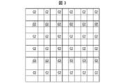
- FIG. 3 is a plan view showing a portion of the optical diffraction element 1 for performing a second optical calculation.
- FIG. 4 is an enlarged perspective view of a part of the optical diffraction element 1.
- the optical diffraction element 1 is a flat plate-shaped optical diffraction element, and is composed of a plurality of microcells (examples of "cells” in the claims) in which the thickness or the refractive index are set independently of each other.
- the "microcell” refers to, for example, a cell having a cell size of less than 10 ⁇ m.
- the "cell size” refers to the square root of the area of the cell. For example, when the plan view shape of the microcell is square, the cell size is the length of one side of the cell.
- the lower limit of the cell size is not particularly limited, but is, for example, 1 nm.
- the plan view shape of the light diffractive element 1 illustrated in FIG. 1 is a square of 12 ⁇ m ⁇ 12 ⁇ m.
- the optical diffraction element 1 is composed of 12 ⁇ 12 microcells C arranged in a matrix.
- the plan view shape of each microcell C is a square of 1 ⁇ m ⁇ 1 ⁇ m.
- the optical diffraction element 1 is divided into 6 ⁇ 6 blocks B arranged in a matrix.
- the plan view shape of each block B is a square of 2 ⁇ m ⁇ 2 ⁇ m.
- Each block B contains 2 ⁇ 2 microcells C arranged in a matrix.
- each block B of the optical diffraction element 1 is composed of K microcells C
- the optical diffraction element 1 can execute a maximum of K optical operations.
- K is any natural number of 2 or more.
- the light diffractive element 1 illustrated in FIG. 1 has a first optical calculation realized by mutual interference of light transmitted through a microcell C1 located at the upper left of each block B and a position at the upper right of each block B.
- the second optical operation (optical operation different from the first optical operation) realized by mutual interference of the light transmitted through the microcell C2 is executed. If only the cell C1 that performs the first optical calculation in the optical diffraction element 1 is extracted and shown, the result will be as shown in FIG. 2.
- each microcell C1 and C2 is composed of a square columnar pillar having a square bottom surface, as shown in FIG.
- the amount of phase change of the light transmitted through the microcell is determined according to the height of the pillar. That is, the amount of phase change of the light transmitted through the microcell composed of the pillars having a high height becomes large, and the amount of the phase change of the light transmitted through the microcell composed of the pillars having a low height becomes small.
- the design of the optical diffraction element 1 is performed as follows. First, when light is incident on each block B of the optical diffraction element 1, the microcell included in each block B is used so that the first optical calculation is performed by the light transmitted through the microcell C1 interfering with each other. Set the thickness or refractive index of C1. At this time, it is assumed that the microcells C2, C3, and C4 included in each block B are masked. Next, when light is incident on each block B of the optical diffraction element 1, the light transmitted through the microcell C2 interferes with each other so that the second optical calculation is performed, and the light is included in each block B. The thickness or refractive index of the microcell C2 is set.
- the thickness or refractive index of the microcell C1 included in each block B can be set by using, for example, machine learning.
- machine learning for example, the intensity distribution of light incident on each block B is input, and the intensity of light generated by the light transmitted through the microcell C1 contained in each block B interfering with each other.
- a model that outputs the distribution and includes the thickness or the refractive index of the microcell C1 contained in each block B as a parameter can be used.
- the thickness or refractive index of the microcell C2 contained in each block B can be similarly realized by using machine learning.
- FIG. 5 is a perspective view showing a configuration of a main part of an optical calculation system 10A that uses the light diffraction element 1 as such a calculation element.
- the optical calculation system 10A includes a light emitting device 2A and a light receiving device 3A in addition to the light diffraction element 1.
- the light emitting device 2A is a device for generating signal light input to the light diffractive element 1.
- the light emitting device 2A has a plurality of light emitting cells arranged in a matrix, and is composed of, for example, a two-dimensional display.
- the light emitting cell of the light emitting device 2A and the block B of the light diffracting element 1 have a one-to-one correspondence.
- the light output from each light emitting cell of the light emitting device 2A is input to the corresponding block B of the light diffracting element 1.
- the light receiving device 3A is a device for detecting the signal light output from the light diffractive element 1.
- the light receiving device 3A has a plurality of light receiving cells arranged in a matrix, and is composed of, for example, a two-dimensional image sensor.
- the light receiving cell of the light receiving device 3A and the block B of the light diffractive element 1 have a one-to-one correspondence.
- the light transmitted through each microcell C1 of the light diffractive element 1 mainly interferes with the light transmitted through the other microcells C1 of the light diffracting element 1 and is input to each light receiving cell of the light receiving device 3A.
- the light transmitted through each microcell C2 of the light diffractive element 1 mainly interferes with the light transmitted through the other microcells C2 of the light diffracting element 1 and is input to each light receiving cell of the light receiving device 3A.
- the signal light detected by each light receiving cell of the light receiving device 3A is the result of the first optical calculation obtained by interfering the light transmitted through the microcell C1 of the light diffracting element 1 with each other, and the light diffracting element 1. It represents the sum with the second calculation result obtained by interfering the light transmitted through the microcell C2 with each other. That is, according to the optical calculation system 10A, a plurality of different optical calculations can be performed, and the sum of the results of these optical calculations can be obtained.
- the present embodiment employs a configuration in which the signal light output from the light diffraction element 1 is immediately input to the light receiving device 3A
- the present invention is not limited to this.
- a single or a plurality of other optical diffractive elements are arranged on the optical path of the signal light output from the optical diffractive element 1, and the light transmitted through these or these optical diffractive elements is input to the light receiving device 3A. May be adopted.
- the optical diffraction element arranged after the optical diffraction element 1 it is preferable to use an optical diffraction element having a lower resolution (larger cell size) than the optical diffraction element 1.
- FIG. 6 is a perspective view showing a configuration of a main part of an optical calculation system 10B that uses the light diffraction element 1 as such a calculation element.
- the optical calculation system 10B includes a light emitting device 2B and a light receiving device 3B in addition to the light diffraction element 1.
- the light emitting device 2B is a device for generating signal light input to the light diffractive element 1.
- the light emitting device 2B has a plurality of light emitting cells arranged in a matrix, and is composed of, for example, a two-dimensional display.
- the light emitting cell of the light emitting device 2B and the block B of the light diffracting element 1 have a one-to-one correspondence.
- the light output from each light emitting cell of the light emitting device 2B is input to the corresponding block B of the light diffracting element 1.
- the light receiving device 3B is a device for detecting the signal light output from the light diffraction element 1.
- the light receiving device 3B has a plurality of light receiving cells arranged in a matrix, and is composed of, for example, a two-dimensional image sensor.
- the light receiving cell of the light receiving device 3B and the microcell C of the light diffracting element 1 have a one-to-one correspondence.
- the light transmitted through each microcell C1 of the light diffractive element 1 mainly interferes with the light transmitted through the other microcells C1 of the light diffracting element 1, and among the light receiving cells of the light receiving device 3B, mainly to the microcell C1. Input to each corresponding light receiving cell.
- each microcell C2 of the optical diffraction element 1 interferes with the light transmitted through the other microcells C2 of the optical diffraction element 1, and among the light receiving cells of the light receiving device 3B, mainly the microcell C2 Is input to each light receiving cell corresponding to.
- the signal light detected by each light receiving cell corresponding to the microcell C1 is the first obtained by interfering the light transmitted through the microcell C1 of the light diffraction element 1 with each other. Represents the result of optical computation.
- the signal light detected by each light receiving cell corresponding to the microcell C2 is the second obtained by interfering the light transmitted through the microcell C2 of the light diffraction element 1 with each other. Represents the result of optical computation. That is, according to the optical calculation system 10B, it is possible to perform a plurality of different optical calculations and obtain the results of these optical calculations.
- the present embodiment employs a configuration in which the signal light output from the light diffraction element 1 is immediately input to the light receiving device 3B
- the present invention is not limited to this.
- a single or a plurality of other optical diffractive elements are arranged on the optical path of the signal light output from the optical diffractive element 1, and the light transmitted through these or these optical diffractive elements is input to the light receiving device 3B. May be adopted.
- the optical diffraction element arranged after the optical diffraction element 1 it is preferable to use an optical diffraction element having a lower resolution (larger cell size) than the optical diffraction element 1.
- the optical diffractive element according to the first aspect of the present invention is an optical diffractive element composed of a plurality of cells whose thicknesses or refractive indexes are set independently of each other, and the plurality of cells are divided into a plurality of blocks.
- Each of the plurality of blocks has a first cell whose thickness or refractive index is set so as to perform a first optical calculation, and a thickness or refractive index is set so as to perform a second optical calculation.
- a second cell is included at least.
- each cell of the optical diffraction element is configured by pillars whose heights are set independently of each other. Has been done.
- an optical diffraction element can be easily manufactured by using nanoimprint technology or the like.
- the optical calculation system is the optical diffractive element according to the first or second aspect and a light emitting device that generates signal light input to the optical diffractive element, and each of the optical diffractive elements.
- a light emitting device composed of a light emitting cell corresponding to a block and a light receiving device for detecting signal light output from the light diffractive element, and a light receiving device composed of a light receiving cell corresponding to each block of the light diffractive element. It is equipped with a device.
- the optical calculation system is the optical diffractive element according to the first or second aspect and a light emitting device that generates signal light input to the optical diffractive element, and each of the optical diffractive elements.
- a light receiving device composed of a light emitting cell corresponding to a block and a light receiving device for detecting signal light output from the light diffractive element, and a light receiving device composed of a light receiving cell corresponding to each cell of the light diffractive element. It is equipped with a device.
- Optical diffractive element B block C Microcell 10A, 10B Optical calculation system 2A, 2B Light emitting device 3A, 3B Light receiving device
Landscapes
- Physics & Mathematics (AREA)
- Engineering & Computer Science (AREA)
- General Physics & Mathematics (AREA)
- Theoretical Computer Science (AREA)
- Optics & Photonics (AREA)
- Mathematical Physics (AREA)
- Nonlinear Science (AREA)
- Health & Medical Sciences (AREA)
- Life Sciences & Earth Sciences (AREA)
- Biomedical Technology (AREA)
- Biophysics (AREA)
- Computing Systems (AREA)
- Computational Linguistics (AREA)
- Data Mining & Analysis (AREA)
- Evolutionary Computation (AREA)
- General Health & Medical Sciences (AREA)
- Molecular Biology (AREA)
- Artificial Intelligence (AREA)
- General Engineering & Computer Science (AREA)
- Neurology (AREA)
- Software Systems (AREA)
- Diffracting Gratings Or Hologram Optical Elements (AREA)
- Investigating Or Analysing Materials By Optical Means (AREA)
- Holo Graphy (AREA)
- Optical Integrated Circuits (AREA)
Abstract
相異なる複数の演算を光学的かつ並列的に実行可能な光回折素子を実現する。光回折素子(1)は、厚み又は屈折率が互いに独立に設定された複数のセル(C)により構成されている。複数のセル(C)は、複数のブロック(B)に分割されており、複数のブロック(B)の各々には、第1の光演算を行うように厚み又は屈折率が設定された第1のセル(C1)と、第2の光演算を行うように厚み又は屈折率が設定された第2のセル(C2)とが、少なくとも含まれている。
Description
本発明は、光演算を行う光回折素子に関する。また、そのような光回折素子を備えた光演算システムに関する。
屈折率が個別に設定された複数のマイクロセルを有し、各マイクロセルを透過した光を相互に干渉させることによって、予め定められた演算を光学的に実行するように設計された光回折素子が知られている。光回折素子を用いた光学的な演算には、プロセッサを用いた電気的な演算と比べて高速且つ低消費電力であるという利点がある。特許文献1には、入力層、中間層、及び出力層を有する光ニューラルネットワークが開示されている。上述した光回折素子は、例えば、このような光ニューラルネットワークの中間層として利用することが可能である。
しかしながら、従来の光回折素子は、特定の光演算を実行することしかできない。すなわち、相異なる複数の演算を光学的且つ並列的に実行する光回折素子は実現されていなかった。
本発明の一態様は、上記の問題に鑑みてなされたものであり、相異なる複数の演算を光学的かつ並列的に実行可能な光回折素子を実現することを目的とする。
本発明の一態様に係る光回折素子は、厚み又は屈折率が互いに独立に設定された複数のセルにより構成された光回折素子であって、前記複数のセルは、複数のブロックに分割されており、前記複数のブロックの各々には、第1の光演算を行うように厚み又は屈折率が設定された第1のセルと、第2の光演算を行うように厚み又は屈折率が設定された第2のセルとが、少なくとも含まれている。
本発明の一態様によれば、相異なる複数の演算を光学的かつ並列的に実行可能な光回折素子を実現することができる。
〔光回折素子の構成〕
本発明の一実施形態に係る光回折素子1の構成について、図1~図4を参照して説明する。図1は、光回折素子1の平面図である。図2は、光回折素子1において第1の光演算を行う部分を示す平面図である。図3は、光回折素子1において第2の光演算を行う部分を示す平面図である。図4は、光回折素子1の一部分を拡大した斜視図である。
本発明の一実施形態に係る光回折素子1の構成について、図1~図4を参照して説明する。図1は、光回折素子1の平面図である。図2は、光回折素子1において第1の光演算を行う部分を示す平面図である。図3は、光回折素子1において第2の光演算を行う部分を示す平面図である。図4は、光回折素子1の一部分を拡大した斜視図である。
光回折素子1は、平板状の光回折素子であり、厚み又は屈折率が互いに独立に設定された複数のマイクロセル(特許請求の範囲における「セル」の一例)により構成されている。ここで、「マイクロセル」とは、例えば、セルサイズが10μm未満のセルのことを指す。また、「セルサイズ」とは、セルの面積の平方根のことを指す。例えば、マイクロセルの平面視形状が正方形である場合、セルサイズとは、セルの一辺の長さである。セルサイズの下限は、特に限定されないが、例えば1nmである。
図1に例示した光回折素子1の平面視形状は、12μm×12μmの正方形である。この光回折素子1は、マトリックス状に配置された12×12個のマイクロセルCにより構成されている。各マイクロセルCの平面視形状は、1μm×1μmの正方形である。また、この光回折素子1は、マトリックス状に配置された6×6個のブロックBに分割されている。各ブロックBの平面視形状は、2μm×2μmの正方形である。各ブロックBは、マトリックス状に配置された2×2個のマイクロセルCを含んでいる。
光回折素子1の各ブロックBがK個のマイクロセルCにより構成されている場合、光回折素子1によって、最大K個の光演算を実行することができる。ここで、Kは、2以上の任意の自然数である。図1に例示した光回折素子1は、各ブロックBの左上に位置するマイクロセルC1を透過した光が相互に干渉することによって実現される第1の光演算と、各ブロックBの右上に位置するマイクロセルC2を透過した光が相互に干渉することによって実現される第2の光演算(第1の光演算とは異なる光演算)と、を実行する。光回折素子1において第1の光演算を行うセルC1のみを抽出して示せば、図2のようになり、光回折素子1において第2の光演算を行うセルC2のみを注して示せば、図3のようになる。なお、本実施形態では実行しないが、各ブロックBの左下に位置するマイクロセルC3を透過した光が相互に干渉することによって実現される第3の光演算を実行することもできるし、各ブロックBの右下に位置するマイクロセルC4を透過した光が相互に干渉することによって実現される第4の光演算を実行することもできる。なお、信号光が画像を表す場合、第1の光演算及び第2の光演算の具体例としては、例えば、畳み込み演算が挙げられる。
光回折素子1を構成する各マイクロセルを透過する光の位相変化量をセル毎に独立に設定する方法としては、(1)マイクロセルの厚みをマイクロセル毎に独立に設定する方法と、(2)マイクロセルの屈折率をマイクロセル毎に独立に選択する方法と、が挙げられる。マイクロセルの屈折率をマイクロセル毎に独立に選択する方法の具体例としては、マイクロセルの材料をマイクロセル毎に独立に選択する方法が挙げられる。本実施形態においては、ナノインプリントにより実現可能な(1)の方法を採用している。この場合、各マイクロセルC1,C2は、図4に示すように、正方形の底面を有する四角柱状のピラーにより構成される。また、この場合、マイクロセルを透過する光の位相変化量は、このピラーの高さに応じて決まる。すなわち、高さの高いピラーにより構成されるマイクロセルを透過する光の位相変化量は大きくなり、高さの低いピラーにより構成されるマイクロセルを透過する光の位相変化量は小さくなる。
光回折素子1の設計は、以下のように行われる。まず、光回折素子1の各ブロックBに光が入射したときに、マイクロセルC1を透過した光が相互に干渉することにより第1の光演算が行われるよう、各ブロックBに含まれるマイクロセルC1の厚み又は屈折率を設定する。この際、各ブロックBに含まれるマイクロセルC2,C3,C4は、マスクされているものとする。次に、光回折素子1の各ブロックBに光が入射したときに、マイクロセルC2を透過した光が相互に干渉することにより第2の光演算が行われるように、各ブロックBに含まれるマイクロセルC2の厚み又は屈折率を設定する。この際、各ブロックBに含まれるマイクロセルC1,C3,C4は、マスクされているものとする。これにより、各ブロックBに光が入射したときに、第1の光演算と第2の光演算とを実行する光回折素子1を実現することができる。
なお、各ブロックBに含まれるマイクロセルC1の厚み又は屈折率の設定は、例えば、機械学習を用いて実現することができる。この機械学習において用いられるモデルとしては、例えば、各ブロックBに入射する光の強度分布を入力とし、各ブロックBに含まれるマイクロセルC1を透過した光が相互に干渉することによって生じる光の強度分布を出力とするモデルであって、各ブロックBに含まれるマイクロセルC1の厚み又は屈折率をパラメータとして含むモデルを用いることができる。各ブロックBに含まれるマイクロセルC2の厚み又は屈折率についても、機械学習を用いて同様に実現することができる。
〔第1の光演算システムの構成〕
光回折素子1は、異なる光演算を並列的に実行する演算素子として利用することができる。図5は、光回折素子1を、このような演算素子として利用する光演算システム10Aの要部構成を示す斜視図である。
光回折素子1は、異なる光演算を並列的に実行する演算素子として利用することができる。図5は、光回折素子1を、このような演算素子として利用する光演算システム10Aの要部構成を示す斜視図である。
光演算システム10Aは、光回折素子1の他に、発光装置2Aと、受光装置3Aと、を備えている。
発光装置2Aは、光回折素子1へと入力される信号光を生成するための装置である。発光装置2Aは、マトリックス状に配置された複数の発光セルを有しており、例えば、2次元ディスプレイにより構成される。発光装置2Aの発光セルと光回折素子1のブロックBとは、1対1に対応している。発光装置2Aの各発光セルから出力された光は、光回折素子1の対応するブロックBに入力される。
受光装置3Aは、光回折素子1から出力される信号光を検出するための装置である。受光装置3Aは、マトリックス状に配置された複数の受光セルを有しており、例えば、2次元イメージセンサにより構成される。受光装置3Aの受光セルと光回折素子1のブロックBとは、1対1に対応している。光回折素子1の各マイクロセルC1を透過した光は、主に光回折素子1の他のマイクロセルC1を透過した光と干渉し、受光装置3Aの各受光セルに入力される。同様に、光回折素子1の各マイクロセルC2を透過した光は、主に光回折素子1の他のマイクロセルC2を透過した光と干渉し、受光装置3Aの各受光セルに入力される。
したがって、受光装置3Aの各受光セルが検出する信号光は、光回折素子1のマイクロセルC1を透過した光を互いに干渉させることにより得られる第1の光演算の結果と、光回折素子1のマイクロセルC2を透過した光を互いに干渉させることにより得られる第2の演算結果との和を表す。すなわち、光演算システム10Aによれば、異なる複数の光演算を行い、これらの光演算の結果の和を得ることができる。
なお、本実施形態においては、光回折素子1から出力される信号光を直ちに受光装置3Aに入力する構成を採用しているが、本発明はこれに限定されない。例えば、光回折素子1から出力される信号光の光路上に単一の又は複数の他の光回折素子を配置し、この又はこれらの光回折素子を透過した光を受光装置3Aに入力する構成を採用してもよい。この場合、光回折素子1の後段に配置される光回折素子としては、光回折素子1よりも分解能が低い(セルサイズが大きい)光回折素子を用いることが好ましい。
〔第2の光演算システムの構成〕
光回折素子1は、異なる光演算を並列的に実行する演算素子として利用することができる。図6は、光回折素子1を、このような演算素子として利用する光演算システム10Bの要部構成を示す斜視図である。
光回折素子1は、異なる光演算を並列的に実行する演算素子として利用することができる。図6は、光回折素子1を、このような演算素子として利用する光演算システム10Bの要部構成を示す斜視図である。
光演算システム10Bは、光回折素子1の他に、発光装置2Bと、受光装置3Bと、を備えている。
発光装置2Bは、光回折素子1へと入力される信号光を生成するための装置である。発光装置2Bは、マトリックス状に配置された複数の発光セルを有しており、例えば、2次元ディスプレイにより構成される。発光装置2Bの発光セルと光回折素子1のブロックBとは、1対1に対応している。発光装置2Bの各発光セルから出力された光は、光回折素子1の対応するブロックBに入力される。
受光装置3Bは、光回折素子1から出力される信号光を検出するための装置である。受光装置3Bは、マトリックス状に配置された複数の受光セルを有しており、例えば、2次元イメージセンサにより構成される。受光装置3Bの受光セルと光回折素子1のマイクロセルCとは、1対1に対応している。光回折素子1の各マイクロセルC1を透過した光は、主に光回折素子1の他のマイクロセルC1を透過した光と干渉し、受光装置3Bの受光セルのうち、主にマイクロセルC1に対応する各受光セルに入力される。同様に、光回折素子1の各マイクロセルC2を透過した光は、光回折素子1の他のマイクロセルC2を透過した光と干渉し、受光装置3Bの受光セルのうち、主にマイクロセルC2に対応する各受光セルに入力される。
したがって、受光装置3Bの受光セルのうち、マイクロセルC1に対応する各受光セルが検出する信号光は、光回折素子1のマイクロセルC1を透過した光を互いに干渉させることにより得られる第1の光演算の結果を表す。一方、受光装置3Bの受光セルのうち、マイクロセルC2に対応する各受光セルが検出する信号光は、光回折素子1のマイクロセルC2を透過した光を互いに干渉させることにより得られる第2の光演算の結果を表す。すなわち、光演算システム10Bによれば、異なる複数の光演算を行い、これらの光演算の結果をそれぞれ得ることができる。
なお、本実施形態においては、光回折素子1から出力される信号光を直ちに受光装置3Bに入力する構成を採用しているが、本発明はこれに限定されない。例えば、光回折素子1から出力される信号光の光路上に単一の又は複数の他の光回折素子を配置し、この又はこれらの光回折素子を透過した光を受光装置3Bに入力する構成を採用してもよい。この場合、光回折素子1の後段に配置される光回折素子としては、光回折素子1よりも分解能が低い(セルサイズが大きい)光回折素子を用いることが好ましい。
(まとめ)
本発明の態様1に係る光回折素子は、厚み又は屈折率が互いに独立に設定された複数のセルにより構成された光回折素子であって、前記複数のセルは、複数のブロックに分割されており、前記複数のブロックの各々には、第1の光演算を行うように厚み又は屈折率が設定された第1のセルと、第2の光演算を行うように厚み又は屈折率が設定された第2のセルとが、少なくとも含まれている。
本発明の態様1に係る光回折素子は、厚み又は屈折率が互いに独立に設定された複数のセルにより構成された光回折素子であって、前記複数のセルは、複数のブロックに分割されており、前記複数のブロックの各々には、第1の光演算を行うように厚み又は屈折率が設定された第1のセルと、第2の光演算を行うように厚み又は屈折率が設定された第2のセルとが、少なくとも含まれている。
上記の構成によれば、相異なる複数の演算を光学的かつ並列的に実行することができる。
本発明の態様2に係る光回折素子においては、態様1の構成に加えて、前記光回折素子の各セルは、高さが互いに独立に設定されたピラーにより構成されている、という構成が採用がされている。
上記の構成によれば、ナノインプリント技術等を用いて光回折素子を容易に製造することができる。
本発明の態様3に係る光演算システムは、態様1又は態様2に係る光回折素子と、前記光回折素子へと入力される信号光を生成する発光装置であって、前記光回折素子の各ブロックに対応する発光セルにより構成された発光装置と、前記光回折素子から出力される信号光を検出する受光装置であって、前記光回折素子の各ブロックに対応する受光セルにより構成された受光装置と、を備えている。
上記の構成によれば、相異なる複数の演算の結果の和を光学的に得ることができる。
本発明の態様4に係る光演算システムは、態様1又は態様2に係る光回折素子と、前記光回折素子へと入力される信号光を生成する発光装置であって、前記光回折素子の各ブロックに対応する発光セルにより構成された発光装置と、前記光回折素子から出力される信号光を検出する受光装置であって、前記光回折素子の各セルに対応する受光セルにより構成された受光装置と、を備えている。
上記の構成によれば、相異なる複数の演算の結果をそれぞれ光学的に得ることができる。
〔付記事項〕
本発明は、上述した実施形態に限定されるものでなく、請求項に示した範囲で種々の変更が可能であり、上述した実施形態にそれぞれ開示された技術的手段を適宜組み合わせて得られる実施形態についても、本発明の技術的範囲に含まれる。
本発明は、上述した実施形態に限定されるものでなく、請求項に示した範囲で種々の変更が可能であり、上述した実施形態にそれぞれ開示された技術的手段を適宜組み合わせて得られる実施形態についても、本発明の技術的範囲に含まれる。
1 光回折素子
B ブロック
C マイクロセル
10A,10B 光演算システム
2A,2B 発光装置
3A,3B 受光装置
B ブロック
C マイクロセル
10A,10B 光演算システム
2A,2B 発光装置
3A,3B 受光装置
Claims (4)
- 厚み又は屈折率が互いに独立に設定された複数のセルにより構成された光回折素子であって、
前記複数のセルは、複数のブロックに分割されており、
前記複数のブロックの各々には、第1の光演算を行うように厚み又は屈折率が設定された第1のセルと、第2の光演算を行うように厚み又は屈折率が設定された第2のセルとが、少なくとも含まれている、
ことを特徴とする光回折素子。 - 前記光回折素子の各セルは、高さが互いに独立に設定されたピラーにより構成されている、
ことを特徴とする請求項1に記載の光回折素子。 - 請求項1又は2に記載の光回折素子と、
前記光回折素子へと入力される信号光を生成する発光装置であって、前記光回折素子の各ブロックに対応する発光セルにより構成された発光装置と、
前記光回折素子から出力される信号光を検出する受光装置であって、前記光回折素子の各ブロックに対応する受光セルにより構成された受光装置と、を備えている、
ことを特徴とする光演算システム。 - 請求項1又は2に記載の光回折素子と、
前記光回折素子へと入力される信号光を生成する発光装置であって、前記光回折素子の各ブロックに対応する発光セルにより構成された発光装置と、
前記光回折素子から出力される信号光を検出する受光装置であって、前記光回折素子の各セルに対応する受光セルにより構成された受光装置と、を備えている、
ことを特徴とする光演算システム。
Priority Applications (4)
| Application Number | Priority Date | Filing Date | Title |
|---|---|---|---|
| CN202180032507.3A CN115485591A (zh) | 2020-12-18 | 2021-08-18 | 光衍射元件及光运算系统 |
| JP2022569707A JP7395774B2 (ja) | 2020-12-18 | 2021-08-18 | 光演算システム |
| EP21906056.3A EP4266092A4 (en) | 2020-12-18 | 2021-08-18 | OPTICAL CALCULATION SYSTEM |
| US17/923,866 US20230176268A1 (en) | 2020-12-18 | 2021-08-18 | Optical diffraction element and optical computing system |
Applications Claiming Priority (2)
| Application Number | Priority Date | Filing Date | Title |
|---|---|---|---|
| JP2020210654 | 2020-12-18 | ||
| JP2020-210654 | 2020-12-18 |
Publications (1)
| Publication Number | Publication Date |
|---|---|
| WO2022130691A1 true WO2022130691A1 (ja) | 2022-06-23 |
Family
ID=82057470
Family Applications (1)
| Application Number | Title | Priority Date | Filing Date |
|---|---|---|---|
| PCT/JP2021/030196 Ceased WO2022130691A1 (ja) | 2020-12-18 | 2021-08-18 | 光回折素子及び光演算システム |
Country Status (5)
| Country | Link |
|---|---|
| US (1) | US20230176268A1 (ja) |
| EP (1) | EP4266092A4 (ja) |
| JP (1) | JP7395774B2 (ja) |
| CN (1) | CN115485591A (ja) |
| WO (1) | WO2022130691A1 (ja) |
Citations (4)
| Publication number | Priority date | Publication date | Assignee | Title |
|---|---|---|---|---|
| US20060050391A1 (en) * | 2004-08-10 | 2006-03-09 | Johan Backlund | Structured-groove diffraction granting and method for control and optimization of spectral efficiency |
| US7847225B2 (en) | 2008-05-02 | 2010-12-07 | Hiroshima University | Optical neural network |
| WO2019009260A1 (ja) * | 2017-07-03 | 2019-01-10 | 大日本印刷株式会社 | 回折光学素子、光照射装置、照射パターンの読取り方法 |
| WO2019173383A1 (en) * | 2018-03-06 | 2019-09-12 | Applied Materials, Inc. | Method of building a 3d functional optical material stacking structure |
Family Cites Families (7)
| Publication number | Priority date | Publication date | Assignee | Title |
|---|---|---|---|---|
| GB2220780B (en) * | 1988-07-05 | 1992-12-23 | Mitsubishi Electric Corp | Neurocomputer |
| US7512573B2 (en) * | 2006-10-16 | 2009-03-31 | Alcatel-Lucent Usa Inc. | Optical processor for an artificial neural network |
| JP4743917B2 (ja) * | 2009-08-25 | 2011-08-10 | Necシステムテクノロジー株式会社 | 光学ユニット |
| EP3776373A4 (en) * | 2018-03-27 | 2022-01-05 | Bar Ilan University | UNIT WITH OPTICAL NEURAL NETWORK AND CONFIGURATION OF OPTICAL NEURAL NETWORK |
| WO2019200289A1 (en) * | 2018-04-13 | 2019-10-17 | The Regents Of The University Of California | Devices and methods employing optical-based machine learning using diffractive deep neural networks |
| WO2020101863A2 (en) * | 2019-10-25 | 2020-05-22 | Futurewei Technologies, Inc. | Hybrid opto-electronic neural networks and methods for utilization thereof |
| US12481305B2 (en) * | 2020-07-03 | 2025-11-25 | Fujikura Ltd. | Optical computing system |
-
2021
- 2021-08-18 EP EP21906056.3A patent/EP4266092A4/en not_active Withdrawn
- 2021-08-18 CN CN202180032507.3A patent/CN115485591A/zh active Pending
- 2021-08-18 US US17/923,866 patent/US20230176268A1/en not_active Abandoned
- 2021-08-18 JP JP2022569707A patent/JP7395774B2/ja active Active
- 2021-08-18 WO PCT/JP2021/030196 patent/WO2022130691A1/ja not_active Ceased
Patent Citations (4)
| Publication number | Priority date | Publication date | Assignee | Title |
|---|---|---|---|---|
| US20060050391A1 (en) * | 2004-08-10 | 2006-03-09 | Johan Backlund | Structured-groove diffraction granting and method for control and optimization of spectral efficiency |
| US7847225B2 (en) | 2008-05-02 | 2010-12-07 | Hiroshima University | Optical neural network |
| WO2019009260A1 (ja) * | 2017-07-03 | 2019-01-10 | 大日本印刷株式会社 | 回折光学素子、光照射装置、照射パターンの読取り方法 |
| WO2019173383A1 (en) * | 2018-03-06 | 2019-09-12 | Applied Materials, Inc. | Method of building a 3d functional optical material stacking structure |
Non-Patent Citations (1)
| Title |
|---|
| See also references of EP4266092A4 |
Also Published As
| Publication number | Publication date |
|---|---|
| JP7395774B2 (ja) | 2023-12-11 |
| EP4266092A1 (en) | 2023-10-25 |
| JPWO2022130691A1 (ja) | 2022-06-23 |
| US20230176268A1 (en) | 2023-06-08 |
| EP4266092A4 (en) | 2024-04-17 |
| CN115485591A (zh) | 2022-12-16 |
Similar Documents
| Publication | Publication Date | Title |
|---|---|---|
| US11293806B2 (en) | Wavefront sensor and method of using it | |
| JP2025106491A5 (ja) | ||
| JP5856727B2 (ja) | 光ビームの波面を解析するための方法、位相格子および装置 | |
| JP2023541447A5 (ja) | ||
| US20250347924A1 (en) | Display System | |
| JP7320124B2 (ja) | 光演算システム | |
| WO2022130691A1 (ja) | 光回折素子及び光演算システム | |
| Behroozinia et al. | Leveraging multiplexed metasurfaces for multi-task learning with all-optical diffractive processors | |
| US12607785B2 (en) | Optical computation system | |
| US12242079B2 (en) | Light diffraction element and optical computing system | |
| WO2022176459A1 (ja) | 光演算装置及び光演算方法 | |
| US20240427165A1 (en) | Optical diffraction element and position adjustment method for optical diffraction element | |
| US20230358928A1 (en) | Optical computing device and optical computing method | |
| Liang et al. | Metasurface-based all-optical diffractive convolutional neural networks | |
| US20240103207A1 (en) | Optical computing device and optical computing method | |
| JP7567022B2 (ja) | 光演算装置及び光演算方法 | |
| Kuo et al. | Optimization of the electron‐beam‐lithography parameters for the moth‐eye effects of an antireflection matrix structure | |
| Doskolovich et al. | Design and investigation of colour separation diffraction gratings | |
| US20240118724A1 (en) | Optical diffraction element, optical computing device, method for adjusting position of optical diffraction element, and method for manufacturing optical computing device | |
| Hollanders | Design Space Exploration of 3D Concrete Printed Bridges | |
| Yu et al. | Dynamic Maclaurin-Series-Based Vision-Language-Action Model | |
| CN121615701A (zh) | 一种用于矩阵计算的集成衍射神经网络及处理器 | |
| JPWO2022130691A5 (ja) | 光演算システム | |
| Xu | Controlling Light at the Nanoscale by Intelligently Designed Artificial Metasurfaces | |
| Tian et al. | Partitionable Diffractive Neural Networks for Multifunctional Optical Operations |
Legal Events
| Date | Code | Title | Description |
|---|---|---|---|
| 121 | Ep: the epo has been informed by wipo that ep was designated in this application |
Ref document number: 21906056 Country of ref document: EP Kind code of ref document: A1 |
|
| ENP | Entry into the national phase |
Ref document number: 2022569707 Country of ref document: JP Kind code of ref document: A |
|
| NENP | Non-entry into the national phase |
Ref country code: DE |
|
| ENP | Entry into the national phase |
Ref document number: 2021906056 Country of ref document: EP Effective date: 20230718 |