WO2022138558A1 - 電子源及びその製造方法、並びに電子源を備える装置 - Google Patents
電子源及びその製造方法、並びに電子源を備える装置 Download PDFInfo
- Publication number
- WO2022138558A1 WO2022138558A1 PCT/JP2021/047021 JP2021047021W WO2022138558A1 WO 2022138558 A1 WO2022138558 A1 WO 2022138558A1 JP 2021047021 W JP2021047021 W JP 2021047021W WO 2022138558 A1 WO2022138558 A1 WO 2022138558A1
- Authority
- WO
- WIPO (PCT)
- Prior art keywords
- tungsten filament
- chip
- electron source
- welded
- electron
- Prior art date
- Legal status (The legal status is an assumption and is not a legal conclusion. Google has not performed a legal analysis and makes no representation as to the accuracy of the status listed.)
- Ceased
Links
Images



Classifications
-
- H—ELECTRICITY
- H01—ELECTRIC ELEMENTS
- H01J—ELECTRIC DISCHARGE TUBES OR DISCHARGE LAMPS
- H01J1/00—Details of electrodes, of magnetic control means, of screens, or of the mounting or spacing thereof, common to two or more basic types of discharge tubes or lamps
- H01J1/02—Main electrodes
- H01J1/13—Solid thermionic cathodes
- H01J1/14—Solid thermionic cathodes characterised by the material
- H01J1/146—Solid thermionic cathodes characterised by the material with metals or alloys as an emissive material
-
- H—ELECTRICITY
- H01—ELECTRIC ELEMENTS
- H01J—ELECTRIC DISCHARGE TUBES OR DISCHARGE LAMPS
- H01J37/00—Discharge tubes with provision for introducing objects or material to be exposed to the discharge, e.g. for the purpose of examination or processing thereof
- H01J37/02—Details
- H01J37/04—Arrangements of electrodes and associated parts for generating or controlling the discharge, e.g. electron-optical arrangement or ion-optical arrangement
- H01J37/06—Electron sources; Electron guns
- H01J37/065—Construction of guns or parts thereof
-
- H—ELECTRICITY
- H01—ELECTRIC ELEMENTS
- H01J—ELECTRIC DISCHARGE TUBES OR DISCHARGE LAMPS
- H01J1/00—Details of electrodes, of magnetic control means, of screens, or of the mounting or spacing thereof, common to two or more basic types of discharge tubes or lamps
- H01J1/02—Main electrodes
- H01J1/13—Solid thermionic cathodes
- H01J1/14—Solid thermionic cathodes characterised by the material
- H01J1/148—Solid thermionic cathodes characterised by the material with compounds having metallic conductive properties, e.g. lanthanum boride, as an emissive material
-
- H—ELECTRICITY
- H01—ELECTRIC ELEMENTS
- H01J—ELECTRIC DISCHARGE TUBES OR DISCHARGE LAMPS
- H01J1/00—Details of electrodes, of magnetic control means, of screens, or of the mounting or spacing thereof, common to two or more basic types of discharge tubes or lamps
- H01J1/02—Main electrodes
- H01J1/13—Solid thermionic cathodes
- H01J1/15—Cathodes heated directly by an electric current
- H01J1/16—Cathodes heated directly by an electric current characterised by the shape
-
- H—ELECTRICITY
- H01—ELECTRIC ELEMENTS
- H01J—ELECTRIC DISCHARGE TUBES OR DISCHARGE LAMPS
- H01J1/00—Details of electrodes, of magnetic control means, of screens, or of the mounting or spacing thereof, common to two or more basic types of discharge tubes or lamps
- H01J1/02—Main electrodes
- H01J1/13—Solid thermionic cathodes
- H01J1/15—Cathodes heated directly by an electric current
- H01J1/18—Supports; Vibration-damping arrangements
-
- H—ELECTRICITY
- H01—ELECTRIC ELEMENTS
- H01J—ELECTRIC DISCHARGE TUBES OR DISCHARGE LAMPS
- H01J2201/00—Electrodes common to discharge tubes
- H01J2201/19—Thermionic cathodes
- H01J2201/196—Emission assisted by other physical processes, e.g. field- or photo emission
-
- H—ELECTRICITY
- H01—ELECTRIC ELEMENTS
- H01J—ELECTRIC DISCHARGE TUBES OR DISCHARGE LAMPS
- H01J2237/00—Discharge tubes exposing object to beam, e.g. for analysis treatment, etching, imaging
- H01J2237/06—Sources
- H01J2237/063—Electron sources
- H01J2237/06308—Thermionic sources
-
- H—ELECTRICITY
- H01—ELECTRIC ELEMENTS
- H01J—ELECTRIC DISCHARGE TUBES OR DISCHARGE LAMPS
- H01J9/00—Apparatus or processes specially adapted for the manufacture, installation, removal, maintenance of electric discharge tubes, discharge lamps, or parts thereof; Recovery of material from discharge tubes or lamps
- H01J9/02—Manufacture of electrodes or electrode systems
- H01J9/04—Manufacture of electrodes or electrode systems of thermionic cathodes
Definitions
- the present disclosure relates to an electron source, a method for manufacturing the electron source, and an apparatus provided with the electron source.
- Electron sources are used, for example, in electron microscopes and semiconductor inspection equipment.
- the electron source comprises a chip composed of an electron emitting material.
- Specific examples of the electron emitting material include a single crystal of LaB 6 (lanthanum hexaboride), a single crystal of HfC, and an IrCe compound.
- the electron source using the LaB 6 single crystal is composed of, for example, a chip of the LaB 6 single crystal, a tungsten filament for heating the chip by energization, and a bonding material for fixing the chip to the tungsten filament. Will be done.
- Production Example 1 of Patent Document 1 describes that an intermediate layer is provided on the lower side surface of a chip of a LaB 6 single crystal using a paste containing TaC powder, and a supporting metal layer is provided using Ta foil. ing.
- a thermionic emission cathode is assembled by spot welding a W wire having a diameter of 150 ⁇ m to the supporting metal layer.
- Patent Document 2 describes a sintered material for an electron beam generating cathode member containing 90% by mass or more of a compound composed of iridium and cerium.
- the present disclosure provides a method for manufacturing an electron source having a structure in which a chip of an electron emitting material is directly bonded to a tungsten filament. Further, the present disclosure provides an electron source capable of suppressing deterioration of the degree of vacuum as compared with a conventional electron source using tantalum for fixing a chip, and capable of obtaining a stable emission current, and an apparatus including the same.
- the method for manufacturing an electron source includes a step of sandwiching an object to be welded, which is overlapped so that a chip of an electron emitting material and a tungsten filament are in direct contact with each other, between a pair of weld electrodes, and a pair of objects to be welded.
- the thickness of the object to be welded is in the range of 50 to 500 ⁇ m, including the step of welding the chip and the tungsten filament by passing a current while applying a pressing force by the welding electrode of the above.
- the electron emitting material include a single crystal of LaB 6 , a single crystal of HfC, and an IrCe compound.
- the IrCe compounds are, for example, Ir2Ce , Ir3Ce , Ir7Ce2 , and Ir5Ce .
- the present inventors directly weld a chip of an electron emitting material (single crystal of LaB 6 ) and a tungsten filament by using a resistance welder having the configurations shown in FIGS. 3 (a) and 3 (b). I tried.
- the thickness of the object to be welded (the total thickness of the tip and the tungsten filament) is in the range of 50 to 500 ⁇ m
- the object to be welded can be locally heated to a high temperature by energization by a pair of welding electrodes.
- the chip and the tungsten filament can be firmly joined by welding.
- the cross-sectional shape of the portion of the chip welded to the tungsten filament is, for example, a square shape or a rectangular shape having a side length of 10 to 300 ⁇ m.
- the electron source according to one aspect of the present disclosure includes a chip of an electron emitting material, a tungsten filament, and a welded portion in which the chip and the tungsten filament are directly bonded, and the thickness of the welded portion is 50 to 500 ⁇ m. Since the chip and the tungsten filament are directly bonded, deterioration of the degree of vacuum can be suppressed and stable emission current can be obtained as compared with the conventional electron source in which a layer containing tantalum is interposed between them. ..
- the tungsten filament in the present disclosure may contain elements other than tungsten (for example, rhenium, aluminum, silicon and potassium) depending on the required performance.
- the device according to one aspect of the present disclosure includes the above electronic source.
- Devices equipped with an electron source include, for example, an electron microscope, a semiconductor manufacturing device, and an inspection device.
- an electron source having a structure in which a chip of an electron emitting material is directly bonded to a tungsten filament. Further, according to the present disclosure, there is provided an electron source capable of suppressing deterioration of the degree of vacuum as compared with a conventional electron source using tantalum for fixing a chip and obtaining a stable emission current, and a device provided with the electron source. do.
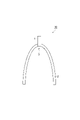
- FIG. 1 is a plan view schematically showing an embodiment of an electron source according to the present disclosure.
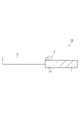
- FIG. 2 is a cross-sectional view schematically showing a welded portion in the electron source shown in FIG.
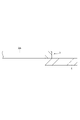
- FIG. 3A is a sectional view schematically showing a state in which an object to be welded, which is overlapped so that a chip and a tungsten filament are in direct contact with each other, is sandwiched between a pair of welding electrodes
- FIG. 3B is a sectional view schematically showing the object to be welded. It is a cross-sectional view schematically showing a state in which a chip and a tungsten filament are welded by passing an electric current while applying a pressing force with a pair of welding electrodes.
- FIG. 1 is a plan view schematically showing an embodiment of an electron source according to the present disclosure.
- FIG. 2 is a cross-sectional view schematically showing a welded portion in the electron source shown in FIG.
- FIG. 3A is a sectional view schematic
- FIG. 4 is a cross-sectional view schematically showing another aspect of the welded portion in the electron source.
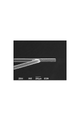
- FIG. 5 is an SEM photograph showing an electron source according to the first embodiment.
- FIG. 6 is an SEM photograph showing an electron source according to the second embodiment.
- FIG. 7 is an SEM photograph showing an electron source according to the third embodiment.
- FIG. 1 is a plan view schematically showing an electron source according to the present embodiment.
- the electron source 10 shown in FIG. 1 includes a chip 1 of LaB 6 , a tungsten filament 2, and a welded portion 3 to which the chip 1 and the tungsten filament 2 are directly bonded.
- the chip 1 is fixed to the top of the tungsten filament 2 bent in a loop shape by welding.
- Examples of the device provided with the electron source 10 include an electron microscope, a semiconductor manufacturing device, an inspection device, and a processing device.
- the chip 1 emits electrons by heating the tungsten filament 2 by energization.
- the chip 1 is preferably a single crystal of LaB 6 and is processed so that the ⁇ 100> direction in which electrons are easily emitted coincides with the electron emission direction.
- the side surface of the chip 1 is preferably a crystal plane of the (100) plane because it is considered that the evaporation rate is slowed down.
- the chip 1 has a substantially rectangular parallelepiped shape.
- the tip of the chip 1 may be processed into a conical shape or a quadrangular pyramid shape. Further, the shape of the chip 1 is not particularly limited, and can be made into a desired shape by electric discharge machining or the like.
- the tungsten filament 2 is for heating the chip 1 by energization.
- the tungsten filament 2 may contain an element other than tungsten (for example, rhenium, aluminum, silicon and potassium) depending on the required performance.
- the tungsten filament 2 may be doped with an alkali metal (for example, potassium) for tissue stabilization.
- the rhenium content of the tungsten filament 2 is, for example, 2 to 30% by mass, and may be 2 to 10% by mass or 2 to 5% by mass. Rhenium has the effect of increasing the electrical resistivity of the tungsten filament 2.
- the welded portion 3 is a portion where the chip 1 and the tungsten filament 2 are joined by welding.
- the welded portion 3 is formed by melting at least one of the chip 1 and the tungsten filament 2 by heating and then solidifying the welded portion 3.
- the thickness of the welded portion 3 (thickness T3 in FIG. 2) is, for example, 50 to 500 ⁇ m, and may be 50 to 400 ⁇ m or 110 to 250 ⁇ m.
- the melting point of the chip 1 is, for example, about 2210 ° C.
- the melting point of the tungsten filament 2 is, for example, about 3422 ° C.
- the electron source 10 is manufactured through the following steps.
- B A step of welding the chip 1 and the tungsten filament 2 by applying an electric current to the object to be welded 5 while applying a pressing force with a pair of welding electrodes 6a and 6b (see FIG. 3B).
- the thickness of the workpiece 5 (the total thickness of the chip 1 and the tungsten filament 2; the thickness T5 in FIG. 3A) is in the range of 50 to 500 ⁇ m, preferably 170 to 400 ⁇ m. It may be 180 to 350 ⁇ m or 180 to 280 ⁇ m.
- the thickness of the work piece 5 is the same as the separation distance between the pair of weld electrodes 6a and 6b in the state where the work piece 5 is sandwiched in the step (A).
- the object to be welded 5 can be locally heated to a high temperature by energization by the pair of weld electrodes 6a and 6b.
- the chip 1 and the tungsten filament 2 can be firmly joined by welding.
- the cross-sectional shape of the portion of the chip 1 to be welded to the tungsten filament 2 is, for example, a square shape or a rectangular shape having a side length of 10 to 300 ⁇ m.
- the length of one side is preferably 60 to 250 ⁇ m, and may be 60 to 200 ⁇ m or 70 to 150 ⁇ m.
- the cross-sectional shape of the portion of the chip 1 to be welded to the tungsten filament 2 may be, for example, a circular shape or an elliptical shape.
- the thickness of the chip 1 in the welding direction is preferably 60 to 250 ⁇ m, and may be 60 to 200 ⁇ m or 70 to 150 ⁇ m.
- the arrow A in FIG. 3A indicates the “welding direction”.
- the cross-sectional shape of the portion of the tungsten filament 2 welded to the chip 1 is, for example, a circular shape or an elliptical shape.
- the thickness of the tungsten filament 2 in the welding direction is preferably 60 to 250 ⁇ m, and may be 60 to 200 ⁇ m or 70 to 150 ⁇ m.
- the cross-sectional shape of the portion of the tungsten filament 2 to be welded to the chip 1 may be, for example, a square shape or a rectangular shape. In this case, the thickness of the tungsten filament 2 in the welding direction is preferably 60 to 250 ⁇ m, and may be 60 to 200 ⁇ m or 70 to 150 ⁇ m.
- the ratio T1 / T2 of the thickness T1 of the chip 1 and the thickness T2 of the tungsten filament 2 is preferably 0.6 to 1.4, and more preferably 0.8 to 1.3.
- the ratio T1 / T2 is within the above range, the region of the workpiece 5 including the interface between the chip 1 and the tungsten filament 2 can be efficiently heated to a high temperature.
- the heating temperature can be adjusted by adjusting the current flowing from the pair of welding electrodes 6a and 6b to the object to be welded 5. At least one of the chip 1 and the tungsten filament 2 may be locally melted by heating by energization, and it is preferable that both the chip 1 and the tungsten filament 2 are locally melted.
- the pressing force applied to the object to be welded 5 from the pair of welding electrodes 6a and 6b may be set to a strength and time sufficient for the chip 1 and the tungsten filament 2 to be firmly bonded.
- the arrow E in FIG. 3B indicates the direction in which the current flows, and the arrow F indicates the direction of the pressing force.
- the electron source manufactured by obtaining the step (B) may be in the form in which the chip 1 is embedded in the tungsten filament 2 as shown in FIG. 2, or as shown in FIG.
- the chip 1 may be bonded to the surface of the tungsten filament 2A.
- the tungsten filament 2A shown in FIG. 4 has a rectangular cross section.
- the chip 1 may be composed of a single crystal of HfC (melting point: 3890 ° C.) or an IrCe compound (IrCe compound).
- the chip 1 may be composed of Ir 2 Ce, Ir 3 Ce, Ir 7 Ce 2 , Ir 5 Ce). Even when these electron emitting materials are used as the chip 1, the chip and the tungsten filament can be firmly bonded by welding.
- LaB 6 chips and tungsten filaments of the following sizes were prepared.
- the tip and tungsten filament were directly welded as follows. First, the chips and the tungsten filaments were superposed so as to be in direct contact with each other, and these were sandwiched between a pair of welding electrodes (see FIG. 3A). Both were welded by applying an electric current to the chip and the tungsten filament while applying a pressing force with a pair of welding electrodes (see FIG. 3 (b)). The welding current was set so that the temperature at the interface between the chip and the tungsten filament exceeded 3422 ° C. (the melting point of tungsten). As a result, as shown in the SEM photograph of FIG. 5, an electron source was obtained in which the chip was firmly bonded to the tungsten filament with the chip embedded in the tungsten filament.
- LaB 6 chips and tungsten filaments of the following sizes were prepared.
- Example 2 HfC chips and tungsten filaments of the following sizes were prepared.
- Example 3 Chips and tungsten filaments of IrCe compound (Ir 7 Ce 2 ) having the following sizes were prepared.
Landscapes
- Chemical & Material Sciences (AREA)
- Analytical Chemistry (AREA)
- Solid Thermionic Cathode (AREA)
- Electron Sources, Ion Sources (AREA)
- Cold Cathode And The Manufacture (AREA)
Abstract
Description
図1は本実施形態に係る電子源を模式的に示す平面図である。図1に示された電子源10は、LaB6のチップ1と、タングステンフィラメント2と、チップ1とタングステンフィラメント2が直接接合している溶接部3とを備える。ループ状に曲げられたタングステンフィラメント2の頂部にチップ1が溶接によって固定されている。電子源10を備える装置として、電子顕微鏡、半導体製造装置、検査装置及び加工装置が挙げられる。
次に、電子源10の製造方法について説明する。電子源10は以下の工程を経て製造される。
(A)チップ1とタングステンフィラメント2が直接接するように重ね合わせた被溶接物5を一対の溶接電極6a,6bで挟み込む工程(図3(a)参照)。
(B)被溶接物5に対して一対の溶接電極6a,6bによって押圧力を加えながら電流を流すことによってチップ1とタングステンフィラメント2を溶接する工程(図3(b)参照)。
以下のサイズのLaB6のチップ及びタングステンフィラメントを準備した。
<LaB6のチップ>
・厚さT1:90μm
・幅:90μm
・長さ:1000μm
<タングステンフィラメント>
・径(厚さT2):127μm
・タングステン純度:99.999質量%以上
以下のサイズのLaB6のチップ及びタングステンフィラメントを準備した。
<LaB6のチップ>
・厚さT1:500μm
・幅:750μm
・長さ:1500μm
<タングステンフィラメント>
・径(厚さT2):127μm
・タングステン純度:99.999質量%以上
以下のサイズのHfCのチップ及びタングステンフィラメントを準備した。
<HfCのチップ>
・厚さT1:90μm
・幅:90μm
・長さ:1000μm
<タングステンフィラメント>
・径(厚さT2):127μm
・タングステン純度:99.999質量%以上
以下のサイズのIrCe化合物(Ir7Ce2)のチップ及びタングステンフィラメントを準備した。
<IrCe化合物のチップ>
・厚さT1:90μm
・幅:90μm
・長さ:1000μm
<タングステンフィラメント>
・径(厚さT2):127μm
・タングステン純度:99.999質量%以上
Claims (8)
- 電子放出材料のチップとタングステンフィラメントが直接接するように重ね合わせた被溶接物を一対の溶接電極で挟み込む工程と、
前記被溶接物に対して前記一対の溶接電極によって押圧力を加えながら電流を流すことによって前記チップと前記タングステンフィラメントを溶接する工程と、
を含み、
前記被溶接物の厚さが50~500μmの範囲である、電子源の製造方法。 - 前記チップにおける前記タングステンフィラメントに対して溶接される部分の断面形状は、一辺の長さが10~300μmの正方形状又は長方形状である、請求項1に記載の電子源の製造方法。
- 前記電子放出材料がLaB6、HfC及びIrCe化合物からなる群から選ばれる一種である、請求項1又は2に記載の電子源の製造方法。
- 前記タングステンフィラメントがレニウムを含有する、請求項1~3のいずれか一項に記載の電子源の製造方法。
- 電子放出材料のチップと、
タングステンフィラメントと、
前記チップと前記タングステンフィラメントが直接接合している溶接部と、
を備え、
前記溶接部の厚さが50~500μmである、電子源。 - 前記電子放出材料がLaB6、HfC及びIrCe化合物からなる群から選ばれる一種である、請求項5に記載の電子源。
- 前記タングステンフィラメントがレニウムを含有する、請求項5又は6に記載の電子源。
- 請求項5~7のいずれか一項に記載の電子源を備える装置。
Priority Applications (5)
| Application Number | Priority Date | Filing Date | Title |
|---|---|---|---|
| EP21910702.6A EP4270441A4 (en) | 2020-12-25 | 2021-12-20 | ELECTRON SOURCE, METHOD FOR PRODUCING SAME AND DEVICE COMPRISING THE ELECTRON SOURCE |
| US18/258,461 US12014894B2 (en) | 2020-12-25 | 2021-12-20 | Electron source, method for manufacturing same, and device provided with electron source |
| JP2022522320A JPWO2022138558A1 (ja) | 2020-12-25 | 2021-12-20 | |
| CN202180068505.XA CN116325060A (zh) | 2020-12-25 | 2021-12-20 | 电子源及其制造方法、以及具备电子源的装置 |
| JP2022207163A JP7781050B2 (ja) | 2020-12-25 | 2022-12-23 | 電子源の製造方法 |
Applications Claiming Priority (2)
| Application Number | Priority Date | Filing Date | Title |
|---|---|---|---|
| JP2020-217530 | 2020-12-25 | ||
| JP2020217530 | 2020-12-25 |
Publications (1)
| Publication Number | Publication Date |
|---|---|
| WO2022138558A1 true WO2022138558A1 (ja) | 2022-06-30 |
Family
ID=82157950
Family Applications (1)
| Application Number | Title | Priority Date | Filing Date |
|---|---|---|---|
| PCT/JP2021/047021 Ceased WO2022138558A1 (ja) | 2020-12-25 | 2021-12-20 | 電子源及びその製造方法、並びに電子源を備える装置 |
Country Status (6)
| Country | Link |
|---|---|
| US (1) | US12014894B2 (ja) |
| EP (1) | EP4270441A4 (ja) |
| JP (2) | JPWO2022138558A1 (ja) |
| CN (1) | CN116325060A (ja) |
| TW (1) | TW202230422A (ja) |
| WO (1) | WO2022138558A1 (ja) |
Cited By (1)
| Publication number | Priority date | Publication date | Assignee | Title |
|---|---|---|---|---|
| WO2025069590A1 (ja) * | 2023-09-27 | 2025-04-03 | 浜松ホトニクス株式会社 | 電子源、これを用いた電子銃及びデバイス |
Families Citing this family (2)
| Publication number | Priority date | Publication date | Assignee | Title |
|---|---|---|---|---|
| EP4270441A4 (en) | 2020-12-25 | 2024-05-22 | Denka Company Limited | ELECTRON SOURCE, METHOD FOR PRODUCING SAME AND DEVICE COMPRISING THE ELECTRON SOURCE |
| JP7783574B2 (ja) * | 2022-03-10 | 2025-12-10 | 三菱自動車工業株式会社 | 組電池 |
Citations (6)
| Publication number | Priority date | Publication date | Assignee | Title |
|---|---|---|---|---|
| JPS5046477A (ja) * | 1973-08-31 | 1975-04-25 | ||
| JPS647450A (en) | 1987-06-30 | 1989-01-11 | Ube Industries | Pointed thermionic emission cathode |
| JPH055306B2 (ja) | 1984-12-28 | 1993-01-22 | Nippon Koden Kogyo Kk | |
| JP2000246451A (ja) * | 1999-03-04 | 2000-09-12 | Noritake Co Ltd | 酸化物被覆フィラメントの溶接機 |
| JP2002358922A (ja) * | 2001-05-31 | 2002-12-13 | Sanken Electric Co Ltd | 冷陰極放電管及びその製法 |
| JP2008262794A (ja) * | 2007-04-12 | 2008-10-30 | National Institute For Materials Science | 希土類六ホウ化物ナノワイヤ熱イオン電子エミッタ |
Family Cites Families (13)
| Publication number | Priority date | Publication date | Assignee | Title |
|---|---|---|---|---|
| JPS51105760A (ja) * | 1975-03-14 | 1976-09-18 | Hitachi Ltd | Chokunetsugatahokabutsuinkyoku no seizohoho |
| US4055780A (en) * | 1975-04-10 | 1977-10-25 | National Institute For Researches In Inorganic Materials | Thermionic emission cathode having a tip of a single crystal of lanthanum hexaboride |
| US4258283A (en) * | 1978-08-31 | 1981-03-24 | Balzers Aktiengesellschaft Fur Hochvakuumtechnik Und Dunne Schichten | Cathode for electron emission |
| US6771013B2 (en) * | 2000-10-17 | 2004-08-03 | Fei Company | Low power schottky emitter |
| WO2009044564A1 (ja) | 2007-10-05 | 2009-04-09 | Denki Kagaku Kogyo Kabushiki Kaisha | 電子源及び電子ビーム装置 |
| JP2010015966A (ja) * | 2008-06-06 | 2010-01-21 | Hitachi High-Technologies Corp | 電子放出素子,電子銃、それを用いた電子顕微鏡装置及び電子線描画装置 |
| JP2010238384A (ja) * | 2009-03-30 | 2010-10-21 | Denki Kagaku Kogyo Kk | 電子源及びその用途 |
| US8896195B2 (en) * | 2010-10-21 | 2014-11-25 | Hermes Microvision, Inc. | Filament for electron source |
| US9165737B2 (en) * | 2012-10-04 | 2015-10-20 | Nuflare Technology, Inc. | High-brightness, long life thermionic cathode and methods of its fabrication |
| JP2015043394A (ja) * | 2013-08-26 | 2015-03-05 | 株式会社ニューフレアテクノロジー | 熱電子放出源の製造方法およびカソードの製造方法 |
| JP6636472B2 (ja) * | 2017-02-28 | 2020-01-29 | 株式会社日立ハイテクノロジーズ | 電子源およびそれを用いた電子線装置 |
| JP6805306B1 (ja) | 2019-09-02 | 2020-12-23 | 株式会社コベルコ科研 | 電子ビーム生成用カソード部材用の焼結材、該焼結材の製造に用いられる溶製材の製造方法、および該焼結材の製造方法 |
| EP4270441A4 (en) | 2020-12-25 | 2024-05-22 | Denka Company Limited | ELECTRON SOURCE, METHOD FOR PRODUCING SAME AND DEVICE COMPRISING THE ELECTRON SOURCE |
-
2021
- 2021-12-20 EP EP21910702.6A patent/EP4270441A4/en not_active Withdrawn
- 2021-12-20 CN CN202180068505.XA patent/CN116325060A/zh active Pending
- 2021-12-20 US US18/258,461 patent/US12014894B2/en active Active
- 2021-12-20 JP JP2022522320A patent/JPWO2022138558A1/ja active Pending
- 2021-12-20 WO PCT/JP2021/047021 patent/WO2022138558A1/ja not_active Ceased
- 2021-12-21 TW TW110147833A patent/TW202230422A/zh unknown
-
2022
- 2022-12-23 JP JP2022207163A patent/JP7781050B2/ja active Active
Patent Citations (6)
| Publication number | Priority date | Publication date | Assignee | Title |
|---|---|---|---|---|
| JPS5046477A (ja) * | 1973-08-31 | 1975-04-25 | ||
| JPH055306B2 (ja) | 1984-12-28 | 1993-01-22 | Nippon Koden Kogyo Kk | |
| JPS647450A (en) | 1987-06-30 | 1989-01-11 | Ube Industries | Pointed thermionic emission cathode |
| JP2000246451A (ja) * | 1999-03-04 | 2000-09-12 | Noritake Co Ltd | 酸化物被覆フィラメントの溶接機 |
| JP2002358922A (ja) * | 2001-05-31 | 2002-12-13 | Sanken Electric Co Ltd | 冷陰極放電管及びその製法 |
| JP2008262794A (ja) * | 2007-04-12 | 2008-10-30 | National Institute For Materials Science | 希土類六ホウ化物ナノワイヤ熱イオン電子エミッタ |
Non-Patent Citations (1)
| Title |
|---|
| See also references of EP4270441A4 |
Cited By (1)
| Publication number | Priority date | Publication date | Assignee | Title |
|---|---|---|---|---|
| WO2025069590A1 (ja) * | 2023-09-27 | 2025-04-03 | 浜松ホトニクス株式会社 | 電子源、これを用いた電子銃及びデバイス |
Also Published As
| Publication number | Publication date |
|---|---|
| EP4270441A1 (en) | 2023-11-01 |
| EP4270441A4 (en) | 2024-05-22 |
| US20240029989A1 (en) | 2024-01-25 |
| CN116325060A (zh) | 2023-06-23 |
| US12014894B2 (en) | 2024-06-18 |
| JPWO2022138558A1 (ja) | 2022-06-30 |
| JP7781050B2 (ja) | 2025-12-05 |
| JP2023036830A (ja) | 2023-03-14 |
| TW202230422A (zh) | 2022-08-01 |
Similar Documents
| Publication | Publication Date | Title |
|---|---|---|
| JP7781050B2 (ja) | 電子源の製造方法 | |
| CN108305823B (zh) | X射线管装置 | |
| US8548124B2 (en) | Electron source and cathode cup thereof | |
| JP7573601B2 (ja) | 電子源及びその製造方法、並びにエミッター及びこれを備える装置 | |
| CN100495633C (zh) | 电子管 | |
| CN105122436B (zh) | 一种半导体封装件及在其上形成半导体接合区的方法 | |
| JP2009146705A (ja) | 電子放出素子、電子源、電子線装置、及び電子放出素子の製造方法 | |
| US12293893B2 (en) | Electron source, manufacturing method therefor, and device comprising electron source | |
| EP4309203A1 (en) | Systems and methods for fabricating silicon die stacks for electron emitter array chips | |
| US12387902B1 (en) | Electrode and filament coupled by adapter | |
| JP7640787B2 (ja) | 電子源及びその製造方法、並びにエミッター及びこれを備える装置 | |
| JP7313791B2 (ja) | 放電ランプ及び放電ランプの電極の製造方法 | |
| KR102742209B1 (ko) | 방전 램프 | |
| EP2847780B1 (en) | An electrically heated planar cathode | |
| TW202518502A (zh) | 發射器 | |
| JP4911526B2 (ja) | 電子源およびその製造方法 | |
| WO2024224548A1 (ja) | 給電部材及びウエハ載置台 | |
| JP2006031976A (ja) | 電界放射電子源およびこれを用いた電子銃 | |
| JP2013134874A (ja) | フィラメント及びその製造方法 | |
| JPH04248233A (ja) | X線管の陰極構体 |
Legal Events
| Date | Code | Title | Description |
|---|---|---|---|
| ENP | Entry into the national phase |
Ref document number: 2022522320 Country of ref document: JP Kind code of ref document: A |
|
| 121 | Ep: the epo has been informed by wipo that ep was designated in this application |
Ref document number: 21910702 Country of ref document: EP Kind code of ref document: A1 |
|
| NENP | Non-entry into the national phase |
Ref country code: DE |
|
| ENP | Entry into the national phase |
Ref document number: 2021910702 Country of ref document: EP Effective date: 20230725 |
|
| WWW | Wipo information: withdrawn in national office |
Ref document number: 2021910702 Country of ref document: EP |