WO2022147966A1 - 晶圆检测方法、装置、设备及存储介质 - Google Patents
晶圆检测方法、装置、设备及存储介质 Download PDFInfo
- Publication number
- WO2022147966A1 WO2022147966A1 PCT/CN2021/100012 CN2021100012W WO2022147966A1 WO 2022147966 A1 WO2022147966 A1 WO 2022147966A1 CN 2021100012 W CN2021100012 W CN 2021100012W WO 2022147966 A1 WO2022147966 A1 WO 2022147966A1
- Authority
- WO
- WIPO (PCT)
- Prior art keywords
- wafer
- image
- picture
- sample
- defect
- Prior art date
- Legal status (The legal status is an assumption and is not a legal conclusion. Google has not performed a legal analysis and makes no representation as to the accuracy of the status listed.)
- Ceased
Links
Images




Classifications
-
- G—PHYSICS
- G06—COMPUTING OR CALCULATING; COUNTING
- G06T—IMAGE DATA PROCESSING OR GENERATION, IN GENERAL
- G06T7/00—Image analysis
- G06T7/0002—Inspection of images, e.g. flaw detection
- G06T7/0004—Industrial image inspection
- G06T7/001—Industrial image inspection using an image reference approach
-
- G—PHYSICS
- G06—COMPUTING OR CALCULATING; COUNTING
- G06T—IMAGE DATA PROCESSING OR GENERATION, IN GENERAL
- G06T7/00—Image analysis
- G06T7/0002—Inspection of images, e.g. flaw detection
- G06T7/0004—Industrial image inspection
-
- G—PHYSICS
- G06—COMPUTING OR CALCULATING; COUNTING
- G06T—IMAGE DATA PROCESSING OR GENERATION, IN GENERAL
- G06T3/00—Geometric image transformations in the plane of the image
- G06T3/40—Scaling of whole images or parts thereof, e.g. expanding or contracting
-
- G—PHYSICS
- G06—COMPUTING OR CALCULATING; COUNTING
- G06T—IMAGE DATA PROCESSING OR GENERATION, IN GENERAL
- G06T7/00—Image analysis
- G06T7/10—Segmentation; Edge detection
-
- H—ELECTRICITY
- H10—SEMICONDUCTOR DEVICES; ELECTRIC SOLID-STATE DEVICES NOT OTHERWISE PROVIDED FOR
- H10P—GENERIC PROCESSES OR APPARATUS FOR THE MANUFACTURE OR TREATMENT OF DEVICES COVERED BY CLASS H10
- H10P74/00—Testing or measuring during manufacture or treatment of wafers, substrates or devices
- H10P74/20—Testing or measuring during manufacture or treatment of wafers, substrates or devices characterised by the properties tested or measured, e.g. structural or electrical properties
- H10P74/203—Structural properties, e.g. testing or measuring thicknesses, line widths, warpage, bond strengths or physical defects
-
- G—PHYSICS
- G06—COMPUTING OR CALCULATING; COUNTING
- G06T—IMAGE DATA PROCESSING OR GENERATION, IN GENERAL
- G06T2207/00—Indexing scheme for image analysis or image enhancement
- G06T2207/20—Special algorithmic details
- G06T2207/20081—Training; Learning
-
- G—PHYSICS
- G06—COMPUTING OR CALCULATING; COUNTING
- G06T—IMAGE DATA PROCESSING OR GENERATION, IN GENERAL
- G06T2207/00—Indexing scheme for image analysis or image enhancement
- G06T2207/20—Special algorithmic details
- G06T2207/20084—Artificial neural networks [ANN]
-
- G—PHYSICS
- G06—COMPUTING OR CALCULATING; COUNTING
- G06T—IMAGE DATA PROCESSING OR GENERATION, IN GENERAL
- G06T2207/00—Indexing scheme for image analysis or image enhancement
- G06T2207/30—Subject of image; Context of image processing
- G06T2207/30108—Industrial image inspection
- G06T2207/30148—Semiconductor; IC; Wafer
Definitions
- the present application relates to the field of semiconductor production, and in particular, to a wafer inspection method, device, equipment and storage medium.
- Wafers are the basic raw materials for manufacturing semiconductor devices. Ultra-high purity semiconductors are prepared into wafers through crystal pulling, slicing and other processes. The wafers undergo a series of semiconductor manufacturing processes to form extremely tiny circuit structures, which are then cut, packaged, and tested to become chips, which are widely used in various electronic equipment. .
- the wafer manufacturing process is extremely complex, mainly including exposure, etching, ion implantation, thin film deposition and chemical mechanical polishing. In actual manufacturing, there are as many as 600 to thousands of steps. There are many types of defects in wafers, in different shapes and sizes. At present, traditional computer vision inspection methods are used to detect defects in wafers, and the detection accuracy is poor, especially for small-scale wafer defects.
- the present application provides a wafer detection method, device, equipment and storage medium, which improve the detection accuracy of wafer defects of different scales.
- an embodiment of the present application provides a wafer inspection method, including:
- the total detection result of the original wafer picture is determined.
- the original wafer picture is divided into pictures to obtain a plurality of first pictures, including:
- a preset sliding window is used to perform image segmentation on the original wafer image to obtain a plurality of first images.
- the size of the original wafer picture is N ⁇ N
- the size of the sliding window is N/n ⁇ N/n
- the size of the original wafer image is N/n ⁇ N/n by using a preset sliding window.
- the circle picture is divided into pictures, and a plurality of first pictures are obtained, including:
- the first detection result includes a first defect location where a wafer defect exists in the second picture, and the second detection result includes a wafer in each of the third pictures. the second defect location of the defect;
- Determining the total detection result of the original wafer picture according to the first detection result and a plurality of the second detection results including:
- the first defect position in the first inspection result and the second defect position in each of the second inspection results are mapped to the coordinate system of the original wafer image to obtain multiple The third defect location;
- the total defect locations in the original wafer image where wafer defects exist are determined.
- the wafer inspection model is based on a deep neural network model and is obtained through training samples.
- the acquisition process of the training samples includes:
- the wafer picture sample and the second segmented picture sample are used as training samples of the wafer detection model.
- the described wafer picture sample is divided into a picture to obtain a plurality of first divided picture samples, including:
- a preset sliding window is used to perform image segmentation on the wafer image samples to obtain a plurality of first segmented image samples.
- the size of the wafer picture sample is N ⁇ N
- the size of the sliding window is N/n ⁇ N/n
- the wafer is analyzed by using a preset sliding window.
- the method further includes:
- an embodiment of the present application provides a wafer inspection device, including:
- the receiving module is used to receive the original wafer picture to be inspected
- a processing module configured to perform picture segmentation on the original wafer picture to obtain a plurality of first pictures, and there is a partial overlap between the plurality of first pictures;
- the total detection result of the original wafer picture is determined.
- the processing module is specifically used for:
- a preset sliding window is used to perform image segmentation on the original wafer image to obtain a plurality of first images.
- the size of the original wafer image is N ⁇ N
- the size of the sliding window is N/n ⁇ N/n
- the processing module is specifically used for:
- n is a positive integer greater than or equal to 2.
- the first detection result includes a first defect location where a wafer defect exists in the second picture, and the second detection result includes a wafer in each of the third pictures.
- the second defect position of the defect; the processing module is specifically used for:
- the first defect position in the first inspection result and the second defect position in each of the second inspection results are mapped to the coordinate system of the original wafer image to obtain multiple The third defect location;
- the total defect locations in the original wafer image where wafer defects exist are determined.
- the apparatus further includes: an acquisition module;
- the obtaining module is configured to obtain a wafer picture sample and a labeling result corresponding to the wafer picture sample, where the labeling result includes a defect position of a wafer defect in the wafer picture sample;
- the processing module is further configured to perform image segmentation on the wafer image samples to obtain a plurality of first segmented image samples
- the wafer picture sample and the second segmented picture sample are used as training samples of the wafer detection model.
- the processing module is specifically configured to: use a preset sliding window to perform image segmentation on the wafer image samples to obtain a plurality of first segmented image samples.
- the size of the wafer image sample is N ⁇ N
- the size of the sliding window is N/n ⁇ N/n
- the processing module is specifically used for:
- the processing module is further configured to:
- an embodiment of the present application provides a wafer inspection device, including:
- the memory stores instructions executable by the at least one processor, the instructions being executed by the at least one processor to enable the wafer inspection apparatus to perform the method of any one of the first aspects .
- an embodiment of the present application provides a computer-readable storage medium, where computer-executable instructions are stored in the computer-readable storage medium, and when the computer-executable instructions are executed by a processor, the processor can be executed The method of any one of the first aspects.
- embodiments of the present application provide a computer program product, including a computer program, where the computer program is executed by a processor to implement the method according to any one of the first aspects.
- Embodiments of the present application provide a wafer inspection method, device, equipment, and storage medium, wherein the inspection method includes: by receiving an original wafer image to be inspected, and performing image segmentation on the original wafer image to obtain a plurality of first images ; Perform image scaling on the original wafer picture and a plurality of first pictures to obtain a second picture and a plurality of third pictures, both of which meet the size requirements of the wafer inspection model for the input picture; The second picture and a plurality of third pictures are sequentially input into the wafer inspection model, and the first inspection result corresponding to the second picture and the second inspection result corresponding to each third picture are obtained; Second, the inspection result determines the total inspection result of the original wafer image.
- the above detection scheme can avoid the loss of defect information caused by image compression, and greatly improves the detection accuracy of small-sized defects while ensuring the detection accuracy of large-sized defects.
- FIG. 1 is a schematic structural diagram of a wafer inspection system provided by an embodiment of the present application.
- FIG. 2 is a schematic flowchart 1 of a wafer inspection method provided by an embodiment of the present application
- FIG. 3 is a second schematic flowchart of a wafer inspection method provided by an embodiment of the present application.
- FIG. 4 is a schematic diagram 1 of dividing an original wafer picture according to an embodiment of the present application.
- FIG. 5 is a second schematic diagram of the segmentation of the original wafer picture provided by the embodiment of the present application.
- FIG. 6 is a flowchart 1 of a wafer inspection model training process provided by an embodiment of the present application.
- FIG. 7 is a flowchart 2 of a wafer inspection model training process provided by an embodiment of the present application.
- FIG. 8 is a schematic structural diagram of a wafer inspection apparatus provided by an embodiment of the present application.
- FIG. 9 is a schematic hardware diagram of a wafer inspection apparatus provided by an embodiment of the present application.
- the technical solutions provided by the embodiments of the present application relate to the field of semiconductor (Semiconductor) wafer (Wafer) production, and in particular, to the field of defect detection (Defect Detection) in the wafer production process.
- semiconductor semiconductor
- Defect Detection field of defect detection
- the chip (ie integrated circuit) industry is a strategic, basic and leading industry for national economic and social development, and plays a key role in several major fields such as computers, consumer electronics, network communications, and automotive electronics.
- the production and manufacturing process of chips is very complex.
- wafers are the main material for manufacturing chips, and their surface defects are the main obstacles that affect the product yield.
- By detecting wafer surface defects not only defective dies can be found, but also faults in the process flow can be judged based on the distribution pattern of defective dies, so that engineers can improve the process.
- wafer defect detection is mainly divided into two categories, one is to detect the electrical properties of the die through probe testing, and the other is to detect defects on the wafer surface through manual visual inspection. Both methods require experienced engineers to analyze and judge, which is labor-intensive, labor-intensive and prone to errors. In the case of the continuous improvement of factory production capacity, the detection efficiency through manual methods is low.
- the detection method mainly includes the following steps: first, feature extraction is performed on the wafer image, and then the extracted features are input into a machine learning model for judgment, and the wafer defects in the wafer image are classified and identified.
- the above-mentioned detection methods have poor effect on wafer defect detection, low accuracy and high false alarm rate.
- an embodiment of the present application proposes a wafer defect detection solution based on a deep neural network model.
- the design divides the original wafer image, zooms the segmented image to meet the model input requirements, and also inputs the image-scaled segmented image into the wafer inspection model, and combines these two types of wafer images to determine the original wafer. Whether there are wafer defects in the circle picture.
- FIG. 1 is a schematic structural diagram of a wafer inspection system provided by an embodiment of the application.
- the wafer inspection system provided by this embodiment includes: a plurality of image acquisition devices, a storage server, At least one resource management node (Fig. 1 shows one resource management node), and a plurality of working nodes.
- each image acquisition device is connected to a storage server
- the storage server is connected to a resource management node
- the resource management server is respectively connected to a plurality of working nodes.
- Each worker node includes multiple graphics processing units (GPUs), which are used to actually perform wafer inspection tasks.
- GPUs graphics processing units
- the image acquisition device of this embodiment is used to collect pictures of each wafer on the production line, and the image acquisition device stores the collected wafer pictures on a storage server.
- the image acquisition device can be set on the inspection machine of the production line.
- the storage server in this embodiment is used to store wafer pictures from different image acquisition devices, and trigger the GPU cluster to perform intelligent defect detection on the wafer pictures.
- the GPU cluster includes a Resource Manager Node (RMN for short) and a Work Node (WN for short).
- the resource management node is responsible for the scheduling of wafer inspection tasks, and the worker nodes are responsible for the execution of wafer inspection tasks.
- the storage server sends the wafer inspection task to the resource management node.
- the wafer inspection task is sent to the GPU that actually executes the task.
- the resource management node assigns the wafer inspection task to the worker node, and the worker node assigns the wafer inspection task to the GPU.
- the resource management node may use a dynamic weight-based polling algorithm to assign wafer inspection tasks to the worker nodes, and periodically check the health status of each worker node connected to the resource management node.
- the wafer detection model is preset in the GPU shown in FIG. 1 , and the model can be obtained by training based on any deep learning model.
- Using the wafer inspection model to detect defects in wafer images requires a lot of computing resources.
- By hardware acceleration on the GPU the performance can be improved by more than 10 times compared to the central processing unit (CPU), which meets the requirements of the wafer inspection model. Real-time requirements for circle detection.
- FIG. 2 is a schematic flow chart 1 of a wafer inspection method provided by an embodiment of the present application.
- the worker node includes two parts: CPU and GPU, and the execution process of the worker node will run on two hardware devices: CPU and GPU.
- the CPU part is responsible for preprocessing the original wafer picture, such as the divided picture in Figure 2, the divided picture can be understood as dividing the original wafer picture into multiple small pictures of the same size.
- the GPU part is responsible for the defect detection task of the wafer image in the wafer inspection task. Before the GPU executes the defect detection task, it first schedules the execution file related to the defect detection task from the CPU.
- the execution file includes the model parameters of the wafer inspection model, etc. Based on the execution file, reasoning is performed on the original wafer image and the divided wafer image to determine whether the original wafer image and the divided wafer image have wafer defects.
- the GPU makes inferences on the divided wafer images through the wafer inspection model. If it is determined that the divided wafer images have wafer defects, the defect coordinates can be mapped to the coordinate system of the original wafer image, and the merged and repeated Defects, determine the defect detection results of the original wafer picture. Finally, the CPU part is responsible for returning the defect detection results of the GPU, thus ending the process.
- the above-mentioned preprocessing further includes at least one of rotation, cropping, scaling, and numerical normalization of the original wafer image.
- data normalization refers to normalizing the RGB value and position information of each pixel of the wafer image to [0, 1].
- the advantage of normalizing to [0, 1] is to make different The data values of the dimensions (RGB value, position) can be compared by the same dimension, so that each feature contributes the same value to the result.
- the preprocessed wafer image meets the requirements of the wafer inspection model for the input image.
- the original wafer image is firstly segmented, and then the original wafer image and the segmented images are inferred one by one.
- the above inference processes are all executed on the GPU to improve the processing speed of model inference.
- FIG. 3 is a second schematic flowchart of a wafer inspection method provided by an embodiment of the present application. As shown in FIG. 3 , the wafer inspection method provided by this embodiment includes the following steps:
- Step 101 Receive a picture of the original wafer to be inspected.
- Step 102 Perform image segmentation on the original wafer image to obtain a plurality of first images.
- a preset sliding window may be used to perform image segmentation on the original wafer image to obtain multiple first images.
- image segmentation is performed on a high-resolution original wafer image (N ⁇ N) to obtain a plurality of low-resolution first images (N/n ⁇ N/n).
- the size of the original wafer image is N ⁇ N
- the size of the sliding window is N/n ⁇ N/n
- the original wafer image is segmented by using a preset sliding window to obtain multiple first images , including: moving the sliding window with N/2n as a step in the first direction and the second direction respectively to obtain (2n-1) ⁇ (2n-1) first pictures.
- the first direction and the second direction are perpendicular to each other.
- N represents the number of pixels, for example, the size of an original wafer image is 2048 ⁇ 2048, and n is a positive integer greater than or equal to 2.
- FIG. 4 is a schematic diagram 1 of dividing a picture of an original wafer according to an embodiment of the present application.
- N ⁇ N high-resolution original wafer image
- n is taken as 2 as an example
- 4 low-resolution first images can be obtained.
- the pictures (N/2 ⁇ N/2) are picture 1 to picture 4 respectively.
- FIG. 5 is a second schematic diagram of dividing the original wafer picture according to the embodiment of the present application.
- N/2n is used as the step size, and n is taken as 2 as an example, (2n-1) ⁇ (2n can be obtained -1), that is, 9 low-resolution first pictures, respectively picture 1 to picture 9.
- move the sliding window N/2 ⁇ N in the first direction, such as the Y direction shown in FIG. 5, and the second direction, such as the X direction shown in FIG. 5, with N/4 as the step size, respectively /2), and obtain pictures 1 to 9 in sequence.
- the X direction and the Y direction are perpendicular to each other.
- the image segmentation method in this embodiment multiple first images are obtained, and there is partial overlap between adjacent first images, so that possible defect information in the original wafer image can be completely retained.
- Step 103 Perform image scaling on the original wafer image to obtain a second image.
- Step 104 performing image scaling on the plurality of first pictures to obtain a plurality of third pictures.
- the second picture in step 103 and the third picture in step 104 have the same picture size, and both meet the size requirements of the wafer inspection model for the input picture.
- step 103 and step 104 in this embodiment is only an example, and the image scaling may also be performed synchronously, or step 104 is performed first and then step 103 is performed.
- the image scaling of the original wafer image generally refers to the image compression of the original wafer image.
- the first picture is obtained by dividing the original wafer picture. Therefore, the size of the first picture is smaller than that of the original wafer picture. If the size of the first picture is smaller than the preset input picture size of the wafer inspection model, the Enlarge the image, and if the size of the first image is larger than the preset input image size of the wafer inspection model, image compression is performed on the first image.
- Step 105 input the second picture and the plurality of third pictures into the wafer inspection model in turn to obtain the first inspection result corresponding to the second picture and the second inspection result corresponding to each third picture.
- the first detection result includes a first defect location with wafer defects in the second picture
- the second detection result includes a second defect location with wafer defects in each of the third pictures.
- the defect position indicates the area of the wafer defect, and the area may be a rectangular area.
- the rectangular area may be represented by diagonal vertex coordinates or four vertex coordinates.
- the inspection result output by the wafer inspection model further includes: a label and a defect category used to indicate whether the input image has wafer defects.
- the label may be a label value, for example, 0 indicates that there is no wafer defect in the input picture, and 1 indicates that there is a wafer defect in the input picture.
- the defect category may be indicated by the ID of the defect category, for example, wafer defects include scratch defects, particle defects, poor coating, poor edge coverage and other defects.
- the detection result further includes a confidence level (which can be understood as a probability value) corresponding to the defect category.
- Step 106 Determine the total inspection result of the original wafer image according to the first inspection result and the plurality of second inspection results.
- the total detection result of the original wafer picture is determined, including:
- the first defect position in the first inspection result and the second defect position in each second inspection result are mapped to the coordinate system of the original wafer image to obtain a plurality of third defect positions; according to the plurality of third defect positions Defect location, to determine the total defect location in the original wafer picture where there are wafer defects.
- the defect positions on the third picture can be mapped to the first picture, and then can be mapped to the original wafer picture.
- the defect positions on the second image can be mapped to the original wafer image.
- the resolution of the third image is low, and the low-resolution image can completely retain the defect information that may exist in the original wafer image, or , the third picture magnifies the small size defects that may exist in the original wafer picture, avoiding the loss of defect information caused by picture compression.
- the resolution of the original wafer image obtained by the Wafer Inspection System (WIS) machine is 2048 ⁇ 2048 pixels
- the optimal input of the wafer inspection model is a 416 ⁇ 416 pixel image.
- the smallest defect identified is 5 ⁇ 5 pixels.
- the compressed small-sized defects cannot be identified (defects are compressed to within 2 ⁇ 2 pixels).
- the original wafer image is divided into a plurality of first images, and the original wafer image and the multiple first images are zoomed. , obtain the second picture and a plurality of third pictures respectively, both the second picture and the third picture meet the size requirements of the wafer inspection model for the input picture; input the second picture and a plurality of third pictures into the wafer inspection model in turn , obtain the first detection result corresponding to the second picture, and the second detection result corresponding to each third picture; and then determine the total detection result of the original wafer picture according to the first detection result and a plurality of second detection results.
- the above detection scheme can avoid the loss of defect information caused by image compression, and greatly improves the detection accuracy of small-sized defects while ensuring the detection accuracy of large-sized defects.
- each GPU of the working node is preset with a wafer detection model.
- the following embodiment describes the training process of the wafer detection model with reference to FIGS. 6 and 7 .
- FIG. 6 is a flowchart 1 of a wafer inspection model training process provided by an embodiment of the present application.
- the creation of training samples mainly includes: obtaining the marked original wafer picture, dividing the original wafer picture, mapping the marking information (ie, mapping the coordinates of the defect position), and removing the non-defective segmented pictures.
- the difference from the existing scheme is that both the original wafer image and the segmented image are put into the training sample set.
- the annotation information can be mapped to the divided image according to the annotation information in the original wafer image.
- the image will be rejected and will not be used for model training.
- the wafer inspection model is trained to determine whether the accuracy of the model meets the preset requirements. If it does not meet the preset requirements, continue to perform model training; if the preset requirements are met, the model training ends. Deploy the trained model on the GPU. Specifically, the model accuracy includes Accuracy, Precision, and Recall. These three parameters must all be greater than or equal to a preset value, such as 90%. It can be determined that the model accuracy meets the preset value. Require. The above three parameters are all controlled by the algorithm.
- the creation of the training sample set can be performed on the CPU, the training and validation of the model can be performed on the GPU, and the trained wafer inspection model can be deployed on the CPU, as shown in FIG. 6 .
- the trained wafer inspection model is deployed on the CPU.
- the wafer inspection can be performed by the GPU in the actual application process.
- the GPU retrieves an execution file from the CPU, that is, a related file of the wafer inspection model deployed on the CPU, and performs wafer inspection based on the retrieved execution file.
- FIG. 7 is a flowchart 2 of a training process of a wafer inspection model provided by an embodiment of the present application.
- the training method of a wafer inspection model includes the following steps:
- Step 201 establishing an initial wafer inspection model.
- Step 202 Obtain training samples and labeling results of the training samples.
- Step 203 Use the training sample as the input of the wafer inspection model, use the labeling result of the training sample as the output of the wafer inspection model, and train the initial wafer inspection model to obtain the wafer inspection model.
- the acquisition process of training samples includes:
- Step 2021 Obtain the wafer image sample and the labeling result corresponding to the wafer image sample, where the labeling result includes the defect location of the wafer defect in the wafer image sample.
- the labeling result corresponding to the wafer image sample further includes the ID of the defect category.
- the wafer image samples include wafer images of different wafer defect types, different wafer defect locations, and different environmental conditions (eg, lighting conditions, temperature environments, humidity environments, etc.).
- Step 2022 Perform image segmentation on the wafer image samples to obtain a plurality of first segmented image samples.
- a preset sliding window may be used to perform image segmentation on the wafer image samples to obtain a plurality of first segmented image samples.
- the size of the wafer image sample is N ⁇ N
- the size of the sliding window is N/n ⁇ N/n
- the sliding window is moved in the first direction and the second direction with N/2n steps respectively.
- Step 2023 According to the defect position in the wafer picture sample, select a second divided picture sample with wafer defects from a plurality of first divided picture samples.
- Step 2024 Use the wafer image sample and the second segmented image sample as training samples of the wafer detection model.
- the acquired training samples should include image samples of different wafer defect categories and image samples of wafer defects of different sizes.
- the wafer image sample or the second divided image sample if the wafer image sample or the second divided image sample does not meet the input size requirements of the wafer inspection model, the wafer image sample or the second divided image sample also needs to be processed as follows:
- Image scaling is performed on the wafer image sample, and the scaled wafer image sample is used as a training sample for the wafer detection model.
- the image scaling of the wafer image sample generally refers to the image compression of the wafer image sample.
- the second divided image sample is obtained by dividing the wafer image sample. Therefore, the size of the second divided image sample is smaller than that of the wafer image sample. If the size of the second divided image sample is smaller than the preset input image size of the wafer inspection model If the size of the second divided image sample is larger than the preset input image size of the wafer inspection model, the second divided image sample is compressed.
- the original wafer image sample and the divided wafer image sample are used as image samples for model training, and the obtained wafer inspection model is trained. Different scales and different types of wafer defects can be accurately identified, which greatly improves the detection accuracy of the detection system for wafer defects of different scales.
- the wafer inspection apparatus can be divided into functional modules according to the above method embodiments.
- each functional module can be divided corresponding to each function, or two or more functions can be integrated into one processing module.
- the above-mentioned integrated modules can be implemented in the form of hardware, or can be implemented in the form of software function modules. It should be noted that, the division of modules in the embodiments of the present application is schematic, and is only a logical function division, and there may be other division manners in actual implementation. The following description will be given by using the division of each function module corresponding to each function as an example.
- FIG. 8 is a schematic structural diagram of a wafer inspection apparatus provided by an embodiment of the present application.
- the wafer inspection apparatus 300 of this embodiment includes:
- the receiving module 301 is used to receive the original wafer picture to be detected
- the processing module 302 is configured to perform picture segmentation on the original wafer picture to obtain a plurality of first pictures, and there is a partial overlap between the plurality of first pictures;
- the total detection result of the original wafer picture is determined.
- the processing module 302 is specifically configured to use a preset sliding window to perform image segmentation on the original wafer image to obtain a plurality of first images.
- the size of the original wafer image is N ⁇ N
- the size of the sliding window is N/n ⁇ N/n
- the processing module is specifically used for:
- n is a positive integer greater than or equal to 2.
- the first detection result includes a first defect location where a wafer defect exists in the second picture, and the second detection result includes a wafer in each of the third pictures.
- the second defect position of the defect; the processing module 302 is specifically used for:
- the first defect position in the first inspection result and the second defect position in each of the second inspection results are mapped to the coordinate system of the original wafer image to obtain multiple The third defect location;
- the total defect locations in the original wafer image where wafer defects exist are determined.
- the apparatus further includes: an obtaining module 303;
- the obtaining module 303 is configured to obtain a wafer image sample and an annotation result corresponding to the wafer image sample, where the annotation result includes a defect location of a wafer defect in the wafer image sample;
- the processing module 302 is further configured to perform image segmentation on the wafer image samples to obtain a plurality of first segmented image samples;
- the wafer picture sample and the second segmented picture sample are used as training samples of the wafer detection model.
- the processing module 302 is specifically configured to: use a preset sliding window to perform image segmentation on the wafer image samples to obtain a plurality of first segmented image samples.
- the size of the wafer image sample is N ⁇ N
- the size of the sliding window is N/n ⁇ N/n
- the processing module 302 is specifically used for:
- the processing module 302 is further configured to:
- the wafer inspection apparatus provided in the embodiment of the present application is used to execute each step of the resource management node in any of the foregoing method embodiments, and the implementation principle and technical effect thereof are similar, which will not be repeated here.
- FIG. 9 is a hardware schematic diagram of a wafer inspection apparatus provided by an embodiment of the present application.
- the wafer inspection apparatus 400 of this embodiment includes:
- processor 401 (only one processor is shown in Figure 9);
- a memory 402 in communication with the at least one processor;
- the memory 402 stores instructions executable by the at least one processor 401, and the instructions are executed by the at least one processor 401, so that the wafer inspection apparatus 400 can perform any of the foregoing method embodiments.
- the memory 402 may be independent or integrated with the processor 401 .
- the wafer inspection apparatus 400 further includes: a bus 403 for connecting the memory 402 and the processor 401 .
- the present application further provides a computer-readable storage medium, where computer-executable instructions are stored in the computer-readable storage medium, and when the computer-executable instructions are executed by a processor, are used to implement the technical solutions of any of the foregoing method embodiments.
- the present application further provides a computer program product, including a computer program, the computer program being executed by a processor to implement the technical solutions of any of the foregoing method embodiments.
- processors mentioned in the embodiments of the present application may be a central processing unit (Central Processing Unit, CPU), and may also be other general-purpose processors, digital signal processors (Digital Signal Processor, DSP), application-specific integrated circuits ( Application Specific Integrated Circuit, ASIC), off-the-shelf Programmable Gate Array (Field Programmable Gate Array, FPGA) or other programmable logic devices, discrete gate or transistor logic devices, discrete hardware components, etc.
- a general purpose processor may be a microprocessor or the processor may be any conventional processor or the like.
- the memory mentioned in the embodiments of the present application may be volatile memory or non-volatile memory, or may include both volatile and non-volatile memory.
- the non-volatile memory may be a read-only memory (Read-Only Memory, ROM), a programmable read-only memory (Programmable ROM, PROM), an erasable programmable read-only memory (Erasable PROM, EPROM), an electrically programmable read-only memory (Erasable PROM, EPROM). Erase programmable read-only memory (Electrically EPROM, EEPROM) or flash memory.
- Volatile memory may be Random Access Memory (RAM), which acts as an external cache.
- RAM Static RAM
- DRAM Dynamic RAM
- SDRAM Synchronous DRAM
- SDRAM double data rate synchronous dynamic random access memory
- Double Data Rate SDRAM DDR SDRAM
- enhanced SDRAM ESDRAM
- synchronous link dynamic random access memory Synchlink DRAM, SLDRAM
- Direct Rambus RAM Direct Rambus RAM
- the processor is a general-purpose processor, DSP, ASIC, FPGA or other programmable logic devices, discrete gate or transistor logic devices, or discrete hardware components
- the memory storage module
- memory described herein is intended to include, but not be limited to, these and any other suitable types of memory.
- the size of the sequence numbers of the above-mentioned processes does not mean the sequence of execution, and the execution sequence of each process should be determined by its functions and internal logic, and should not be dealt with in the embodiments of the present application. implementation constitutes any limitation.
Landscapes
- Engineering & Computer Science (AREA)
- Physics & Mathematics (AREA)
- General Physics & Mathematics (AREA)
- Theoretical Computer Science (AREA)
- Computer Vision & Pattern Recognition (AREA)
- Quality & Reliability (AREA)
- Testing Or Measuring Of Semiconductors Or The Like (AREA)
- Investigating Materials By The Use Of Optical Means Adapted For Particular Applications (AREA)
Abstract
一种晶圆检测方法、装置、设备及存储介质,其中,检测方法包括:通过接收待检测的原始晶圆图片,对原始晶圆图片进行图片分割,得到多张第一图片;对原始晶圆图片和多张第一图片进行图片缩放,分别得到第二图片和多张第三图片,第二图片和第三图片均满足晶圆检测模型对输入图片的尺寸要求;将第二图片和多张第三图片依次输入晶圆检测模型中,得到第二图片对应的第一检测结果,以及每张第三图片对应的第二检测结果;再根据第一检测结果以及多个第二检测结果,确定原始晶圆图片的总检测结果。可避免图片压缩造成缺陷信息的丢失,在保证大尺寸缺陷的检测精度的同时,大幅提高了小尺寸缺陷的检测精度。
Description
本申请要求于2021年01月08日提交中国专利局、申请号为202110022536.3、申请名称为“晶圆检测方法、装置、设备及存储介质”的中国专利申请的优先权,其全部内容通过引用结合在本申请中。
本申请涉及半导体生产领域,尤其涉及一种晶圆检测方法、装置、设备及存储介质。
晶圆(wafer)是制造半导体器件的基础性原材料。极高纯度的半导体经过拉晶、切片等工序制备成为晶圆,晶圆经过一系列半导体制造工艺形成极微小的电路结构,再经切割、封装、测试成为芯片,广泛应用到各类电子设备当中。
晶圆制造工艺极其复杂,主要包括曝光、蚀刻、离子注入、薄膜沉积和化学机械研磨等步骤,在实际生产制造中多达六百到上千个步骤。晶圆的缺陷种类众多,形状大小各异。目前,采用传统的计算机视觉检测方式,对晶圆的缺陷检测效果不佳,尤其是对于小尺度的晶圆缺陷,检测精度差。
发明内容
本申请提供一种晶圆检测方法、装置、设备及存储介质,提高对不同尺度晶圆缺陷的检测精度。
第一方面,本申请实施例提供一种晶圆检测方法,包括:
接收待检测的原始晶圆图片;
对所述原始晶圆图片进行图片分割,得到多张第一图片,所述多张第一图片之间存在部分重叠;
对所述原始晶圆图片进行图片缩放,得到第二图片;
对多张所述第一图片进行图片缩放,得到多张第三图片;
将所述第二图片以及多张所述第三图片依次输入晶圆检测模型中,得到所述第二图片对应的第一检测结果,以及每张所述第三图片对应的第二检测结果;
根据所述第一检测结果以及多个所述第二检测结果,确定所述原始晶圆图片的总检测结果。
在本申请的一个实施例中,所述对所述原始晶圆图片进行图片分割,得到多张第一图片,包括:
采用预设的滑动窗口对所述原始晶圆图片进行图片分割,得到多张第一图片。
在本申请的一个实施例中,所述原始晶圆图片的尺寸为N×N,所述滑动窗口的尺寸为N/n×N/n,所述采用预设的滑动窗口对所述原始晶圆图片进行图片分割,得到多张第一图片,包括:
分别在第一方向和第二方向上以N/2n为步长,移动所述滑动窗口,得到(2n-1) ×(2n-1)张所述第一图片,其中,所述第一方向与所述第二方向相互垂直,n为大于或等于2的正整数。
在本申请的一个实施例中,所述第一检测结果包括所述第二图片中存在晶圆缺陷的第一缺陷位置,所述第二检测结果包括每张所述第三图片中存在晶圆缺陷的第二缺陷位置;
所述根据所述第一检测结果以及多个所述第二检测结果,确定所述原始晶圆图片的总检测结果,包括:
将所述第一检测结果中的所述第一缺陷位置,以及每个所述第二检测结果中的所述第二缺陷位置,映射到所述原始晶圆图片的坐标系中,得到多个第三缺陷位置;
根据所述多个第三缺陷位置,确定所述原始晶圆图片中存在晶圆缺陷的总的缺陷位置。
在本申请的一个实施例中,所述晶圆检测模型是基于深度神经网络模型,经过训练样本训练得到的,所述训练样本的获取过程,包括:
获取晶圆图片样本以及所述晶圆图片样本对应的标注结果,所述标注结果包括晶圆图片样本中存在晶圆缺陷的缺陷位置;
对所述晶圆图片样本进行图片分割,得到多张第一分割图片样本;
根据所述晶圆图片样本中所述缺陷位置,从所述多张第一分割图片样本中选取存在晶圆缺陷的第二分割图片样本;
将所述晶圆图片样本以及所述第二分割图片样本作为所述晶圆检测模型的训练样本。
在本申请的一个实施例中,所述对所述晶圆图片样本进行图片分割,得到多张第一分割图片样本,包括:
采用预设的滑动窗口对所述晶圆图片样本进行图片分割,得到多张第一分割图片样本。
在本申请的一个实施例中,所述晶圆图片样本的尺寸为N×N,所述滑动窗口的尺寸为N/n×N/n,所述采用预设的滑动窗口对所述晶圆图片样本进行图片分割,得到多张第一分割图片样本,包括:
分别在第一方向和第二方向上以N/2n为步长,移动所述滑动窗口,得到(2n-1)×(2n-1)张所述第一分割图片样本,所述第一方向与所述第二方向相互垂直。
在本申请的一个实施例中,若所述晶圆图片样本或者所述第二分割图片样本不满足所述晶圆检测模型的输入尺寸要求,所述方法还包括:
对所述晶圆图片样本进行图片缩放,将缩放后的晶圆图片样本作为所述晶圆检测模型的一个训练样本;或者
对所述第二分割图片样本进行图片缩放,将缩放后的第二分割图片样本作为所述晶圆检测模型的一个训练样本。
第二方面,本申请实施例提供一种晶圆检测装置,包括:
接收模块,用于接收待检测的原始晶圆图片;
处理模块,用于对所述原始晶圆图片进行图片分割,得到多张第一图片,所述多张第一图片之间存在部分重叠;
对所述原始晶圆图片进行图片缩放,得到第二图片;
对多张所述第一图片进行图片缩放,得到多张第三图片;
将所述第二图片以及多张所述第三图片依次输入晶圆检测模型中,得到所述第二图片对应的第一检测结果,以及每张所述第三图片对应的第二检测结果;
根据所述第一检测结果以及多个所述第二检测结果,确定所述原始晶圆图片的总检测结果。
在本申请的一个实施例中,所述处理模块,具体用于:
采用预设的滑动窗口对所述原始晶圆图片进行图片分割,得到多张第一图片。
在本申请的一个实施例中,所述原始晶圆图片的尺寸为N×N,所述滑动窗口的尺寸为N/n×N/n,所述处理模块,具体用于:
分别在第一方向和第二方向上以N/2n为步长,移动所述滑动窗口,得到(2n-1)×(2n-1)张所述第一图片,其中,所述第一方向与所述第二方向相互垂直,n为大于或等于2的正整数。
在本申请的一个实施例中,所述第一检测结果包括所述第二图片中存在晶圆缺陷的第一缺陷位置,所述第二检测结果包括每张所述第三图片中存在晶圆缺陷的第二缺陷位置;所述处理模块,具体用于:
将所述第一检测结果中的所述第一缺陷位置,以及每个所述第二检测结果中的所述第二缺陷位置,映射到所述原始晶圆图片的坐标系中,得到多个第三缺陷位置;
根据所述多个第三缺陷位置,确定所述原始晶圆图片中存在晶圆缺陷的总的缺陷位置。
在本申请的一个实施例中,所述装置还包括:获取模块;
所述获取模块,用于获取晶圆图片样本以及所述晶圆图片样本对应的标注结果,所述标注结果包括晶圆图片样本中存在晶圆缺陷的缺陷位置;
所述处理模块,还用于对所述晶圆图片样本进行图片分割,得到多张第一分割图片样本;
根据所述晶圆图片样本中所述缺陷位置,从所述多张第一分割图片样本中选取存在晶圆缺陷的第二分割图片样本;
将所述晶圆图片样本以及所述第二分割图片样本作为所述晶圆检测模型的训练样本。
在本申请的一个实施例中,所述处理模块,具体用于:采用预设的滑动窗口对所述晶圆图片样本进行图片分割,得到多张第一分割图片样本。
在本申请的一个实施例中,所述晶圆图片样本的尺寸为N×N,所述滑动窗口的尺寸为N/n×N/n,所述处理模块,具体用于:
分别在第一方向和第二方向上以N/2n为步长,移动所述滑动窗口,得到(2n-1)×(2n-1)张所述第一分割图片样本,所述第一方向与所述第二方向相互垂直。
在本申请的一个实施例中,若所述晶圆图片样本或者所述第二分割图片样本不满足所述晶圆检测模型的输入尺寸要求,所述处理模块,还用于:
对所述晶圆图片样本进行图片缩放,将缩放后的晶圆图片样本作为所述晶圆检测模型的一个训练样本;或者
对所述第二分割图片样本进行图片缩放,将缩放后的第二分割图片样本作为所述晶圆检测模型的一个训练样本。
第三方面,本申请实施例提供一种晶圆检测设备,包括:
至少一个处理器;以及
与所述至少一个处理器通信连接的存储器;其中,
所述存储器存储有可被所述至少一个处理器执行的指令,所述指令被所述至少一个处理器执行,以使所述晶圆检测设备能够执行第一方面中任一项所述的方法。
第四方面,本申请实施例提供一种计算机可读存储介质,所述计算机可读存储介质中存储有计算机执行指令,当所述计算机执行指令被处理器执行时,使得所述处理器能够执行第一方面中任一项所述的方法。
第五方面,本申请实施例提供一种计算机程序产品,包括计算机程序,所述计算机程序被处理器执行以实现如第一方面中任一项所述的方法。
本申请实施例提供一种晶圆检测方法、装置、设备及存储介质,其中,检测方法包括:通过接收待检测的原始晶圆图片,对原始晶圆图片进行图片分割,得到多张第一图片;对原始晶圆图片和多张第一图片进行图片缩放,分别得到第二图片和多张第三图片,第二图片和第三图片均满足晶圆检测模型对输入图片的尺寸要求;将第二图片和多张第三图片依次输入晶圆检测模型中,得到第二图片对应的第一检测结果,以及每张第三图片对应的第二检测结果;再根据第一检测结果以及多个第二检测结果,确定原始晶圆图片的总检测结果。上述检测方案可避免图片压缩造成缺陷信息的丢失,在保证大尺寸缺陷的检测精度的同时,大幅提高了小尺寸缺陷的检测精度。
图1为本申请实施例提供的一种晶圆检测系统的架构示意图;
图2为本申请实施例提供的晶圆检测方法的流程示意图一;
图3为本申请实施例提供的晶圆检测方法的流程示意图二;
图4为本申请实施例提供的对原始晶圆图片的分割示意图一;
图5为本申请实施例提供的对原始晶圆图片的分割示意图二;
图6为本申请实施例提供的晶圆检测模型训练过程的流程图一;
图7为本申请实施例提供的晶圆检测模型训练过程的流程图二;
图8为本申请实施例提供的一种晶圆检测装置的结构示意图;
图9为本申请实施例提供的一种晶圆检测装置的硬件示意图。
下面将结合本申请实施例中的附图,对本申请实施例中的技术方案进行清楚、完整地描述,显然,所描述的实施例仅仅是本申请一部分实施例,而不是全部的实施例。基于本申请中的实施例,本领域普通技术人员在没有做出创造性劳动前提下所获得的所有其他实施例,都属于本申请保护的范围。
本申请的说明书和权利要求书及上述附图中的术语“第一”、“第二”等是用于区别类似的对象,而不必用于描述特定的顺序或先后次序。应该理解这样使用的数据在适当情况下可以互换,以便这里描述的本申请的实施例例如能够以除了在这里图示或描述的那些 以外的顺序实施。
此外,术语“包括”和“具有”以及他们的任何变形,意图在于覆盖不排他的包含,例如,包含了一系列步骤或单元的过程、方法、系统、产品或设备不必限于清楚地列出的那些步骤或单元,而是可包括没有清楚地列出的或对于这些过程、方法、产品或设备固有的其它步骤或单元。
本申请实施例提供的技术方案涉及半导体(Semiconductor)晶圆(Wafer)生产领域,特别涉及晶圆生产过程中的缺陷检测(Defect Detection)领域。
芯片(即集成电路)产业是国民经济和社会发展的战略性、基础性、先导性产业,在计算机、消费类电子、网络通信、汽车电子等几大领域起着关键作用。芯片的生产制造流程非常复杂,其中,晶圆作为制造芯片的主要材料,其表面缺陷是影响产品良率的主要障碍。通过检测晶圆表面缺陷,不仅能发现有缺陷的晶粒,还能根据缺陷晶粒的分布模式判断工艺流程中存在的故障,以便工程师进行工艺上的改良。
目前,晶圆缺陷检测主要分为两类,一是通过探针测试检测晶粒的电气性能,二是通过人工目检检测晶圆表面的缺陷。这两种方式均需要经验丰富的工程师进行分析判断,耗费人力、劳动强度大且容易出现误差。在工厂产能不断提升的情况下,通过人工方式的检测效率低。
随着检测技术的不断发展,出现基于图像识别的检测方法,能够一定程度上提升晶圆检测的效率和准确率。该检测方法主要包括如下几个步骤:首先对晶圆图片进行特征提取,然后提取的特征输入到机器学习模型中进行判断,分类识别出晶圆图片的晶圆缺陷。然而,上述检测方法对晶圆的缺陷检测效果不佳,准确率低,误报率高。
随后,出现基于深度学习的检测方法,深度学习作为目前最热的机器学习方法,需要大量的训练数据,与上述图像识别的检测方法相比,能够进一步提升晶圆检测准确率,降低误报率。然而,晶圆缺陷类型众多,有大尺寸的划痕(scratch)缺陷,也有小尺寸的颗粒(particle)缺陷,对于晶圆图片中出现的小尺寸的缺陷,例如10×10像素以内,在满足深度学习模型对输入图片尺寸要求的情况下,小尺寸的缺陷可能由于图片的压缩而无法被识别到,造成缺陷信息的丢失。
针对上述问题,本申请实施例提出了一种基于深度神经网络模型的晶圆缺陷检测方案,除了将原始的晶圆图片压缩后输入晶圆检测模型之外,考虑到小尺寸的晶圆缺陷,设计将原始的晶圆图片进行图片分割,将分割后的图片缩放至模型输入要求,将经图片缩放的分割图片也输入晶圆检测模型中,结合这两种类型的晶圆图片确定原始的晶圆图片中是否存在晶圆缺陷。
在介绍本申请实施例提供的晶圆检测方法之前,首先对该方法的系统架构进行简要介绍。
示例性的,图1为本申请实施例提供的一种晶圆检测系统的架构示意图,如图1所示,本实施例提供的晶圆检测系统,包括:多个图像采集设备,存储服务器,至少一个资源管理节点(图1示出一个资源管理节点),多个工作节点。其中,每个图像采集设备与存储服务器连接,存储服务器与资源管理节点连接,资源管理服务器分别与多个工作节点连接。每个工作节点包括多个图像处理器(graphics processing unit,GPU),GPU用于实际执行晶圆检测任务。
本实施例的图像采集设备,用于采集产线上每个晶圆的图片,图像采集设备将采集的晶圆图片存储到存储服务器上。作为一种示例,图像采集设备可以设置在产线的检测机台上。
本实施例的存储服务器用于存储来自不同图像采集设备的晶圆图片,并触发GPU集群对晶圆图片进行智能缺陷检测。其中,GPU集群包括资源管理节点(Resource Manager Node,简称RMN)和工作节点(Work Node,简称WN)。资源管理节点负责晶圆检测任务的调度,工作节点负责晶圆检测任务的执行。
在本申请的一个实施例中,存储服务器向资源管理节点发送晶圆检测任务。通过两级调度算法,将晶圆检测任务下发至实际执行任务的GPU。具体的,资源管理节点将晶圆检测任务分配给工作节点,工作节点再将晶圆检测任务分配给GPU。
在本申请的一个实施例中,资源管理节点可采用基于动态权重的轮询算法将晶圆检测任务分配给工作节点,并定期检查与资源管理节点连接的各个工作节点的健康状况。
作为一种示例,图1所示的GPU中预置晶圆检测模型,该模型可以是基于任意深度学习模型训练得到的。使用晶圆检测模型检测晶圆图片中的缺陷需要耗费大量计算资源,通过在GPU上进行硬件加速,相比于中央处理器(central processing unit,CPU),性能提升可以达到10倍以上,满足晶圆检测的实时性要求。
下面以具体地实施例对本申请的技术方案进行详细说明。下面这几个具体的实施例可以相互结合,对于相同或相似的概念或过程可能在某些实施例不再赘述。
示例性的,图2为本申请实施例提供的晶圆检测方法的流程示意图一,如图2所示,本实施例提供的晶圆检测方法可应用于图1所示的任意一个工作节点,工作节点包括CPU和GPU两部分,工作节点的执行流程会在CPU和GPU两种硬件设备上运行。其中,CPU部分负责对原始晶圆图片进行预处理,例如图2中的分割图片,分割图片可以理解为将原始晶圆图片分割成多张尺寸相同的小图片。GPU部分负责晶圆检测任务中晶圆图片的缺陷检测任务,GPU在执行缺陷检测任务之前,首先从CPU中调度缺陷检测任务相关的执行文件,该执行文件包括晶圆检测模型的模型参数等,基于该执行文件,对原始晶圆图片以及分割后的晶圆图片进行推理,确定原始晶圆图片以及分割后的晶圆图片是否存在晶圆缺陷。
需要说明的是,GPU通过晶圆检测模型对分割后的晶圆图片进行推理,若确定分割后的晶圆图片存在晶圆缺陷,可将缺陷坐标映射至原晶圆图片的坐标系,合并重复缺陷,确定原始晶圆图片的缺陷检测结果。最后,CPU部分负责返回GPU的缺陷检测结果,从而结束流程。
可选的,在一些实施例中,上述预处理还包括对原始晶圆图片的旋转、裁剪、缩放、数值归一化的至少一项。其中,数据归一化是指将晶圆图片的每个像素点的RGB值和位置信息都归一化到[0,1]之间,归一化到[0,1]的好处是让不同维度的数据值(RGB值,位置)可以通过相同的量纲进行比较,使得各个特征对结果的贡献值相同。经过预处理后的晶圆图片满足晶圆检测模型对输入图片的要求。
从上述实施例的描述可知,在晶圆检测模型的推理阶段,首先对原始晶圆图片进行图片分割,再对原始晶圆图片和分割后的图片进行逐一推理,如果分割后的图片中检测到晶圆缺陷,将缺陷的坐标系映射至原图的坐标系。由于分割后的图片存在交叠部分,重复缺 陷需要进行合并处理。上述推理过程都是在GPU上执行,以提高模型推理的处理速度。
在图2所示实施例的基础上,下面通过一个具体实施例,对晶圆检测模型的模型输入、模型推理过程进行详细的说明。示例性的,图3为本申请实施例提供的晶圆检测方法的流程示意图二,如图3所示,本实施例提供的晶圆检测方法包括如下步骤:
步骤101、接收待检测的原始晶圆图片。
步骤102、对原始晶圆图片进行图片分割,得到多张第一图片。
其中,多张第一图片之间存在部分重叠。
在本申请的一个实施例中,可采用预设的滑动窗口对原始晶圆图片进行图片分割,得到多张第一图片。示例性的,对高分辨率的原始晶圆图片(N×N)进行图片分割,得到多张低分辨率的第一图片(N/n×N/n)。
作为一种示例,原始晶圆图片的尺寸为N×N,滑动窗口的尺寸为N/n×N/n,采用预设的滑动窗口对原始晶圆图片进行图片分割,得到多张第一图片,包括:分别在第一方向和第二方向上以N/2n为步长,移动滑动窗口,得到(2n-1)×(2n-1)张第一图片。其中,第一方向与第二方向相互垂直。N表示像素数,例如某一原始晶圆图片的尺寸为2048×2048,n为大于或等于2的正整数。
示例性的,图4为本申请实施例提供的对原始晶圆图片的分割示意图一。如图4所示,对于高分辨率的原始晶圆图片(N×N)进行图片分割,如果采用N/n为步长,以n取2为例,可以得到4张低分辨率的第一图片(N/2×N/2),分别为图片1至图片4。
示例性的,图5为本申请实施例提供的对原始晶圆图片的分割示意图二。如图5所示,对于高分辨率的原始晶圆图片(N×N)进行图片分割,如果采用N/2n为步长,以n取2为例,可以得到(2n-1)×(2n-1)张,即9张低分辨率的第一图片,分别为图片1至图片9。具体的,分别在第一方向,例如图5所示的Y方向,以及第二方向,例如图5所示的X方向上,以N/4为步长,移动滑动窗口(N/2×N/2),依次得到图片1至图片9。其中,X方向与Y方向相互垂直。通过本实施例的图片分割方法,得到多张第一图片,相邻的第一图片之间存在部分重叠,这样可以完全保留原始晶圆图片中可能存在的缺陷信息。
步骤103、对原始晶圆图片进行图片缩放,得到第二图片。
步骤104、对多张第一图片进行图片缩放,得到多张第三图片。
步骤103中的第二图片与步骤104中的第三图片的图片尺寸相同,均满足晶圆检测模型对输入图片的尺寸要求。
需要说明的是,本实施例中步骤103和步骤104的执行顺序仅作为一种示例,还可以同步进行图片缩放,或者,先执行步骤104再执行步骤103。
需要说明的是,通常情况下,原始晶圆图片的尺寸大于晶圆检测模型预设的输入图片尺寸,因此,对原始晶圆图片的图片缩放一般指对原始晶圆图片的图片压缩。第一图片是对原始晶圆图片进行图片分割得到的,因此第一图片的尺寸小于原始晶圆图片,若第一图片的尺寸小于晶圆检测模型预设的输入图片尺寸,则对第一图片进行图片放大,若第一图片的尺寸大于晶圆检测模型预设的输入图片尺寸,则对第一图片进行图片压缩。
步骤105、将第二图片以及多张第三图片依次输入晶圆检测模型中,得到第二图片对应的第一检测结果,以及每张第三图片对应的第二检测结果。
在本实施例中,第一检测结果包括第二图片中存在晶圆缺陷的第一缺陷位置,第二检 测结果包括每张第三图片中存在晶圆缺陷的第二缺陷位置。缺陷位置指示晶圆缺陷的区域,该区域可以是一矩形区域,相应的,矩形区域可通过对角顶点坐标或者四个顶点坐标表示。
可选的,在一些实施例中,晶圆检测模型输出的检测结果还包括:用于指示输入图片是否存在晶圆缺陷的标签以及缺陷类别。
示例性的,标签可以是标签值,例如0表示输入图片中不存在晶圆缺陷,1表示输入图片中存在晶圆缺陷。缺陷类别可通过缺陷类别的ID指示,示例性的,晶圆缺陷包括划痕缺陷,颗粒缺陷,镀膜不良,边缘覆盖差等缺陷。
可选的,在一些实施例中,检测结果还包括缺陷类别对应的置信度(可以理解为概率值)。
步骤106、根据第一检测结果以及多个第二检测结果,确定原始晶圆图片的总检测结果。
在本申请的一个实施例中,根据第一检测结果以及多个第二检测结果,确定原始晶圆图片的总检测结果,包括:
将第一检测结果中的第一缺陷位置,以及每个第二检测结果中的第二缺陷位置,映射到原始晶圆图片的坐标系中,得到多个第三缺陷位置;根据多个第三缺陷位置,确定原始晶圆图片中存在晶圆缺陷的总的缺陷位置。
由于第一图片是原始晶圆图片分割得到的,第三图片是通过第一图片缩放得到的,第三图片上的缺陷位置可以映射至第一图片,进而可以映射至原始晶圆图片。由于第二图片是原始晶圆图片缩放得到的,第二图片上的缺陷位置可以映射至原始晶圆图片。通过对缺陷位置的坐标映射,将第二图片以及每个第三图片的缺陷检测结果合并,剔除重复的缺陷位置,从而得到原始晶圆图片中存在晶圆缺陷的总的缺陷位置。
需要说明的是,相比于通过原始晶圆图片直接缩放得到的第二图片,第三图片的分辨率低,低分辨率的图片可以完全保留原始晶圆图片中可能存在的缺陷信息,或者说,第三图片放大了原始晶圆图片中可能存在的小尺寸缺陷,避免了图片压缩造成的缺陷信息的丢失。
示例性的,晶圆检测系统(Wafer Inspection System,WIS)机台获取的原始晶圆图片的分辨率为2048×2048像素,晶圆检测模型的最佳输入为416×416像素的图片,目前可识别的最小缺陷为5×5像素,对于原始晶圆图片中出现的小尺寸缺陷(10×10像素以内),压缩后的小尺寸缺陷无法识别(缺陷被压缩至2×2像素以内)。对此,考虑将原始晶圆图片进行图片分割,得到多张分辨率为512×512像素的第一图片,随后将第一图片压缩到分辨率为416×416像素的第三图片,如此一来,第三图片中的小尺寸缺陷不会由于压缩比例过大而无法被检测到。
本实施例提供的晶圆检测方法,通过接收待检测的原始晶圆图片,对原始晶圆图片进行图片分割,得到多张第一图片;对原始晶圆图片和多张第一图片进行图片缩放,分别得到第二图片和多张第三图片,第二图片和第三图片均满足晶圆检测模型对输入图片的尺寸要求;将第二图片和多张第三图片依次输入晶圆检测模型中,得到第二图片对应的第一检测结果,以及每张第三图片对应的第二检测结果;再根据第一检测结果以及多个第二检测结果,确定原始晶圆图片的总检测结果。上述检测方案可避免图片压缩造成缺陷信息的丢失,在保证大尺寸缺陷的检测精度的同时,大幅提高了小尺寸缺陷的检测精度。
由上述实施例可知,工作节点的每个GPU中均预置晶圆检测模型,下面一个实施例结合附图6、7对晶圆检测模型的训练过程进行说明。
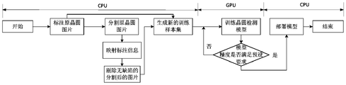
示例性的,图6为本申请实施例提供的晶圆检测模型训练过程的流程图一,如图6所示,在对晶圆检测模型进行训练之前,首先需要创建一定数量的训练样本。具体的,训练样本的创建主要包括:获取标注的原晶圆图片、分割原晶圆图片、映射标注信息(即映射缺陷位置坐标)、剔除无缺陷的分割后的图片。与现有方案的不同之处在于,原晶圆图片和分割后的图片均被放入训练样本集中。可根据原晶圆图片中的标注信息,对分割后的图片映射标注信息。在一些实施例中,为了尽量减少训练样本集的图片数量,如果分割后的图片不存在晶圆缺陷,该图片将被剔除,不会进入模型训练。
基于创建好的训练样本集,对晶圆检测模型进行训练,判断模型精度是否满足预设要求,若不满足预设要求,则继续执行模型训练;若满足预设要求,则模型训练结束,在GPU上部署训练好的模型。具体的,模型精度包括Accuracy(准确率),Precision(查准度),Recall(查全度),这三个参数必须都大于或等于预设值,例如90%,可确定模型精度满足预设要求。上述三个参数都是由算法控制的。
在一种可能的实施方式中,训练样本集的创建可以在CPU上执行,模型的训练和验证可以在GPU上执行,训练好的晶圆检测模型可部署在CPU上,如图6所示。
需要说明的是,将训练好的晶圆检测模型部署在CPU上,为了提高晶圆检测速度,可在实际应用过程中,由GPU执行晶圆检测。具体的,GPU从CPU中调取执行文件,即CPU上部署的晶圆检测模型的相关文件,基于调取的执行文件进行晶圆检测。
示例性的,图7为本申请实施例提供的晶圆检测模型训练过程的流程图二,如图7所示,晶圆检测模型的训练方法,包括如下步骤:
步骤201、建立初始的晶圆检测模型。
步骤202、获取训练样本以及训练样本的标注结果。
步骤203、将训练样本作为晶圆检测模型的输入,将训练样本的标注结果作为晶圆检测模型的输出,对初始的晶圆检测模型进行训练,得到晶圆检测模型。
本实施例中,训练样本的获取过程,包括:
步骤2021、获取晶圆图片样本以及晶圆图片样本对应的标注结果,标注结果包括晶圆图片样本中存在晶圆缺陷的缺陷位置。
可选的,在一些实施例中,晶圆图片样本对应的标注结果还包括缺陷类别的ID。本实施例中,晶圆图像样本包括不同晶圆缺陷类别、不同晶圆缺陷位置、不同环境条件(例如光照条件、温度环境、湿度环境等)的晶圆图片。
步骤2022、对晶圆图片样本进行图片分割,得到多张第一分割图片样本。
具体的,可采用预设的滑动窗口对晶圆图片样本进行图片分割,得到多张第一分割图片样本。
作为一种示例,晶圆图片样本的尺寸为N×N,滑动窗口的尺寸为N/n×N/n,分别在第一方向和第二方向上以N/2n为步长,移动滑动窗口,得到(2n-1)×(2n-1)张第一分割图片样本,如图5所示,第一方向为Y方向,第二方向为X方向,第一方向与第二方向相互垂直。
步骤2023、根据晶圆图片样本中缺陷位置,从多张第一分割图片样本中选取存在晶圆 缺陷的第二分割图片样本。
步骤2024、将晶圆图片样本以及第二分割图片样本作为晶圆检测模型的训练样本。
在本实施例中,获取的训练样本应包含不同晶圆缺陷类别的图片样本、不同尺寸的晶圆缺陷的图片样本。
可选的,在一些实施例中,若晶圆图片样本或者第二分割图片样本不满足晶圆检测模型的输入尺寸要求,还需要对晶圆图片样本或第二分割图片样本进行如下处理:
对晶圆图片样本进行图片缩放,将缩放后的晶圆图片样本作为晶圆检测模型的一个训练样本。或者
对第二分割图片样本进行图片缩放,将缩放后的第二分割图片样本作为晶圆检测模型的一个训练样本。
需要说明的是,通常情况下,晶圆图片样本的尺寸大于晶圆检测模型预设的输入图片尺寸,因此,对晶圆图片样本的图片缩放一般指对晶圆图片样本的图片压缩。第二分割图片样本是对晶圆图片样本进行图片分割得到的,因此第二分割图片样本的尺寸小于晶圆图片样本,若第二分割图片样本的尺寸小于晶圆检测模型预设的输入图片尺寸,则对第二分割图片样本进行图片放大,若第二分割图片样本的尺寸大于晶圆检测模型预设的输入图片尺寸,则对第二分割图片样本进行图片压缩。
本实施例提供的晶圆检测模型的训练方法,考虑到小尺寸的晶圆缺陷,将原晶圆图片样本以及分割后的晶圆图片样本作为模型训练的图片样本,训练得到的晶圆检测模型可以准确识别不同尺度、不同类型的晶圆缺陷,大大提高了检测系统对不同尺度晶圆缺陷的检测精度。
本申请实施例可以根据上述方法实施例对晶圆检测装置进行功能模块的划分,例如,可以对应各个功能划分各个功能模块,也可以将两个或两个以上的功能集成在一个处理模块中。上述集成的模块既可以使用硬件的形式实现,也可以使用软件功能模块的形式实现。需要说明的是,本申请实施例中对模块的划分是示意性的,仅仅为一种逻辑功能划分,实际实现时可以有另外的划分方式。下面以使用对应各个功能划分各个功能模块为例进行说明。
示例性的,图8为本申请实施例提供的一种晶圆检测装置的结构示意图。如图8所示,本实施例的晶圆检测装置300,包括:
接收模块301,用于接收待检测的原始晶圆图片;
处理模块302,用于对所述原始晶圆图片进行图片分割,得到多张第一图片,所述多张第一图片之间存在部分重叠;
对所述原始晶圆图片进行图片缩放,得到第二图片;
对多张所述第一图片进行图片缩放,得到多张第三图片;
将所述第二图片以及多张所述第三图片依次输入晶圆检测模型中,得到所述第二图片对应的第一检测结果,以及每张所述第三图片对应的第二检测结果;
根据所述第一检测结果以及多个所述第二检测结果,确定所述原始晶圆图片的总检测结果。
在本申请的一个实施例中,所述处理模块302,具体用于采用预设的滑动窗口对所述原始晶圆图片进行图片分割,得到多张第一图片。
在本申请的一个实施例中,所述原始晶圆图片的尺寸为N×N,所述滑动窗口的尺寸为N/n×N/n,所述处理模块,具体用于:
分别在第一方向和第二方向上以N/2n为步长,移动所述滑动窗口,得到(2n-1)×(2n-1)张所述第一图片,其中,所述第一方向与所述第二方向相互垂直,n为大于或等于2的正整数。
在本申请的一个实施例中,所述第一检测结果包括所述第二图片中存在晶圆缺陷的第一缺陷位置,所述第二检测结果包括每张所述第三图片中存在晶圆缺陷的第二缺陷位置;所述处理模块302,具体用于:
将所述第一检测结果中的所述第一缺陷位置,以及每个所述第二检测结果中的所述第二缺陷位置,映射到所述原始晶圆图片的坐标系中,得到多个第三缺陷位置;
根据所述多个第三缺陷位置,确定所述原始晶圆图片中存在晶圆缺陷的总的缺陷位置。
在本申请的一个实施例中,所述装置还包括:获取模块303;
所述获取模块303,用于获取晶圆图片样本以及所述晶圆图片样本对应的标注结果,所述标注结果包括晶圆图片样本中存在晶圆缺陷的缺陷位置;
所述处理模块302,还用于对所述晶圆图片样本进行图片分割,得到多张第一分割图片样本;
根据所述晶圆图片样本中所述缺陷位置,从所述多张第一分割图片样本中选取存在晶圆缺陷的第二分割图片样本;
将所述晶圆图片样本以及所述第二分割图片样本作为所述晶圆检测模型的训练样本。
在本申请的一个实施例中,所述处理模块302,具体用于:采用预设的滑动窗口对所述晶圆图片样本进行图片分割,得到多张第一分割图片样本。
在本申请的一个实施例中,所述晶圆图片样本的尺寸为N×N,所述滑动窗口的尺寸为N/n×N/n,所述处理模块302,具体用于:
分别在第一方向和第二方向上以N/2n为步长,移动所述滑动窗口,得到(2n-1)×(2n-1)张所述第一分割图片样本,所述第一方向与所述第二方向相互垂直。
在本申请的一个实施例中,若所述晶圆图片样本或者所述第二分割图片样本不满足所述晶圆检测模型的输入尺寸要求,所述处理模块302,还用于:
对所述晶圆图片样本进行图片缩放,将缩放后的晶圆图片样本作为所述晶圆检测模型的一个训练样本;或者
对所述第二分割图片样本进行图片缩放,将缩放后的第二分割图片样本作为所述晶圆检测模型的一个训练样本。
本申请实施例提供的晶圆检测装置,用于执行前述任一方法实施例中资源管理节点的各个步骤,其实现原理和技术效果类似,在此不再赘述。
示例性的,图9为本申请实施例提供的一种晶圆检测设备的硬件示意图。如图9所示,本实施例的晶圆检测设备400,包括:
至少一个处理器401(图9中仅示出了一个处理器);以及
与所述至少一个处理器通信连接的存储器402;其中,
所述存储器402存储有可被所述至少一个处理器401执行的指令,所述指令被所述至少一个处理器401执行,以使所述晶圆检测设备400能够执行前述任一方法实施例中资源 管理节点的各个步骤。
可选的,存储器402既可以是独立的,也可以跟处理器401集成在一起。
当存储器402是独立于处理器401之外的器件时,晶圆检测设备400还包括:总线403,用于连接存储器402和处理器401。
本申请还提供一种计算机可读存储介质,所述计算机可读存储介质中存储有计算机执行指令,当所述计算机执行指令被处理器执行时用于实现前述任一方法实施例的技术方案。
本申请还提供一种计算机程序产品,包括计算机程序,所述计算机程序被处理器执行以实现前述任一方法实施例的技术方案。
应理解,本申请实施例中提及的处理器可以是中央处理单元(Central Processing Unit,CPU),还可以是其他通用处理器、数字信号处理器(Digital Signal Processor,DSP)、专用集成电路(Application Specific Integrated Circuit,ASIC)、现成可编程门阵列(Field Programmable Gate Array,FPGA)或者其他可编程逻辑器件、分立门或者晶体管逻辑器件、分立硬件组件等。通用处理器可以是微处理器或者该处理器也可以是任何常规的处理器等。
还应理解,本申请实施例中提及的存储器可以是易失性存储器或非易失性存储器,或可包括易失性和非易失性存储器两者。其中,非易失性存储器可以是只读存储器(Read-Only Memory,ROM)、可编程只读存储器(Programmable ROM,PROM)、可擦除可编程只读存储器(Erasable PROM,EPROM)、电可擦除可编程只读存储器(Electrically EPROM,EEPROM)或闪存。易失性存储器可以是随机存取存储器(Random Access Memory,RAM),其用作外部高速缓存。通过示例性但不是限制性说明,许多形式的RAM可用,例如静态随机存取存储器(Static RAM,SRAM)、动态随机存取存储器(Dynamic RAM,DRAM)、同步动态随机存取存储器(Synchronous DRAM,SDRAM)、双倍数据速率同步动态随机存取存储器(Double Data Rate SDRAM,DDR SDRAM)、增强型同步动态随机存取存储器(Enhanced SDRAM,ESDRAM)、同步连接动态随机存取存储器(Synchlink DRAM,SLDRAM)和直接内存总线随机存取存储器(Direct Rambus RAM,DR RAM)。
需要说明的是,当处理器为通用处理器、DSP、ASIC、FPGA或者其他可编程逻辑器件、分立门或者晶体管逻辑器件、分立硬件组件时,存储器(存储模块)集成在处理器中。
应注意,本文描述的存储器旨在包括但不限于这些和任意其它适合类型的存储器。
应理解,在本申请的各种实施例中,上述各过程的序号的大小并不意味着执行顺序的先后,各过程的执行顺序应以其功能和内在逻辑确定,而不应对本申请实施例的实施过程构成任何限定。
以上所述,仅为本申请的具体实施方式,但本申请的保护范围并不局限于此,任何熟悉本技术领域的技术人员在本申请揭露的技术范围内,可轻易想到变化或替换,都应涵盖在本申请的保护范围之内。因此,本申请的保护范围应所述以权利要求的保护范围为准。
Claims (17)
- 一种晶圆检测方法,包括:接收待检测的原始晶圆图片;对所述原始晶圆图片进行图片分割,得到多张第一图片,所述多张第一图片之间存在部分重叠;对所述原始晶圆图片进行图片缩放,得到第二图片;对多张所述第一图片进行图片缩放,得到多张第三图片;将所述第二图片以及多张所述第三图片依次输入晶圆检测模型中,得到所述第二图片对应的第一检测结果,以及每张所述第三图片对应的第二检测结果;根据所述第一检测结果以及多个所述第二检测结果,确定所述原始晶圆图片的总检测结果。
- 根据权利要求1所述的方法,其中,所述对所述原始晶圆图片进行图片分割,得到多张第一图片,包括:采用预设的滑动窗口对所述原始晶圆图片进行图片分割,得到多张第一图片。
- 根据权利要求2所述的方法,其中,所述原始晶圆图片的尺寸为N×N,所述滑动窗口的尺寸为N/n×N/n,所述采用预设的滑动窗口对所述原始晶圆图片进行图片分割,得到多张第一图片,包括:分别在第一方向和第二方向上以N/2n为步长,移动所述滑动窗口,得到(2n-1)×(2n-1)张所述第一图片,其中,所述第一方向与所述第二方向相互垂直,n为大于或等于2的正整数。
- 根据权利要求1所述的方法,其中,所述第一检测结果包括所述第二图片中存在晶圆缺陷的第一缺陷位置,所述第二检测结果包括每张所述第三图片中存在晶圆缺陷的第二缺陷位置;所述根据所述第一检测结果以及多个所述第二检测结果,确定所述原始晶圆图片的总检测结果,包括:将所述第一检测结果中的所述第一缺陷位置,以及每个所述第二检测结果中的所述第二缺陷位置,映射到所述原始晶圆图片的坐标系中,得到多个第三缺陷位置;根据所述多个第三缺陷位置,确定所述原始晶圆图片中存在晶圆缺陷的总的缺陷位置。
- 根据权利要求1所述的方法,其中,所述晶圆检测模型是基于深度神经网络模型,经过训练样本训练得到的,所述训练样本的获取过程,包括:获取晶圆图片样本以及所述晶圆图片样本对应的标注结果,所述标注结果包括晶圆图片样本中存在晶圆缺陷的缺陷位置;对所述晶圆图片样本进行图片分割,得到多张第一分割图片样本;根据所述晶圆图片样本中所述缺陷位置,从所述多张第一分割图片样本中选取存在晶圆缺陷的第二分割图片样本;将所述晶圆图片样本以及所述第二分割图片样本作为所述晶圆检测模型的训练样本。
- 根据权利要求5所述的方法,其中,所述对所述晶圆图片样本进行图片分割,得到多张第一分割图片样本,包括:采用预设的滑动窗口对所述晶圆图片样本进行图片分割,得到多张第一分割图片样本。
- 根据权利要求6所述的方法,其中,所述晶圆图片样本的尺寸为N×N,所述滑动窗口的尺寸为N/n×N/n,所述采用预设的滑动窗口对所述晶圆图片样本进行图片分割,得到多张第一分割图片样本,包括:分别在第一方向和第二方向上以N/2n为步长,移动所述滑动窗口,得到(2n-1)×(2n-1)张所述第一分割图片样本,所述第一方向与所述第二方向相互垂直。
- 根据权利要求5所述的方法,其中,若所述晶圆图片样本或者所述第二分割图片样本不满足所述晶圆检测模型的输入尺寸要求,所述方法还包括:对所述晶圆图片样本进行图片缩放,将缩放后的晶圆图片样本作为所述晶圆检测模型的一个训练样本;或者对所述第二分割图片样本进行图片缩放,将缩放后的第二分割图片样本作为所述晶圆检测模型的一个训练样本。
- 一种晶圆检测装置,包括:接收模块,用于接收待检测的原始晶圆图片;处理模块,用于对所述原始晶圆图片进行图片分割,得到多张第一图片,所述多张第一图片之间存在部分重叠;对所述原始晶圆图片进行图片缩放,得到第二图片;对多张所述第一图片进行图片缩放,得到多张第三图片;将所述第二图片以及多张所述第三图片依次输入晶圆检测模型中,得到所述第二图片对应的第一检测结果,以及每张所述第三图片对应的第二检测结果;根据所述第一检测结果以及多个所述第二检测结果,确定所述原始晶圆图片的总检测结果。
- 根据权利要求9所述的装置,其中,所述处理模块,具体用于:采用预设的滑动窗口对所述原始晶圆图片进行图片分割,得到多张第一图片。
- 根据权利要求10所述的装置,其中,所述原始晶圆图片的尺寸为N×N,所述滑动窗口的尺寸为N/n×N/n,所述处理模块,具体用于:分别在第一方向和第二方向上以N/2n为步长,移动所述滑动窗口,得到(2n-1)×(2n-1)张所述第一图片,其中,所述第一方向与所述第二方向相互垂直,n为大于或等于2的正整数。
- 根据权利要求9所述的装置,其中,所述第一检测结果包括所述第二图片中存在晶圆缺陷的第一缺陷位置,所述第二检测结果包括每张所述第三图片中存在晶圆缺陷的第二缺陷位置;所述处理模块,具体用于:将所述第一检测结果中的所述第一缺陷位置,以及每个所述第二检测结果中的所述第二缺陷位置,映射到所述原始晶圆图片的坐标系中,得到多个第三缺陷位置;根据所述多个第三缺陷位置,确定所述原始晶圆图片中存在晶圆缺陷的总的缺陷位置。
- 根据权利要求9所述的装置,其中,所述装置还包括:获取模块;所述获取模块,用于获取晶圆图片样本以及所述晶圆图片样本对应的标注结果,所述标注结果包括晶圆图片样本中存在晶圆缺陷的缺陷位置;所述处理模块,还用于对所述晶圆图片样本进行图片分割,得到多张第一分割图片样本;根据所述晶圆图片样本中所述缺陷位置,从所述多张第一分割图片样本中选取存在晶圆缺陷的第二分割图片样本;将所述晶圆图片样本以及所述第二分割图片样本作为所述晶圆检测模型的训练样本。
- 根据权利要求13所述的装置,其中,所述处理模块,具体用于:采用预设的滑动窗口对所述晶圆图片样本进行图片分割,得到多张第一分割图片样本。
- 根据权利要求14所述的装置,其中,所述晶圆图片样本的尺寸为N×N,所述滑动窗口的尺寸为N/n×N/n,所述处理模块,具体用于:分别在第一方向和第二方向上以N/2n为步长,移动所述滑动窗口,得到(2n-1)×(2n-1)张所述第一分割图片样本,所述第一方向与所述第二方向相互垂直。
- 根据权利要求13所述的装置,其中,若所述晶圆图片样本或者所述第二分割图片样本不满足所述晶圆检测模型的输入尺寸要求,所述处理模块,还用于:对所述晶圆图片样本进行图片缩放,将缩放后的晶圆图片样本作为所述晶圆检测模型的一个训练样本;或者对所述第二分割图片样本进行图片缩放,将缩放后的第二分割图片样本作为所述晶圆检测模型的一个训练样本。
- 一种晶圆检测设备,包括:至少一个处理器;以及与所述至少一个处理器通信连接的存储器;其中,所述存储器存储有可被所述至少一个处理器执行的指令,所述指令被所述至少一个处理器执行,以使所述晶圆检测设备能够执行权利要求1-8中任一项所述的方法。
Priority Applications (2)
| Application Number | Priority Date | Filing Date | Title |
|---|---|---|---|
| EP21769326.6A EP4050560B1 (en) | 2021-01-08 | 2021-06-15 | Wafer testing method and apparatus, and device and storage medium |
| US17/401,595 US11928808B2 (en) | 2021-01-08 | 2021-08-13 | Wafer detection method, device, apparatus, and storage medium |
Applications Claiming Priority (2)
| Application Number | Priority Date | Filing Date | Title |
|---|---|---|---|
| CN202110022536.3 | 2021-01-08 | ||
| CN202110022536.3A CN114764770B (zh) | 2021-01-08 | 2021-01-08 | 晶圆检测方法、装置、设备及存储介质 |
Related Child Applications (1)
| Application Number | Title | Priority Date | Filing Date |
|---|---|---|---|
| US17/401,595 Continuation US11928808B2 (en) | 2021-01-08 | 2021-08-13 | Wafer detection method, device, apparatus, and storage medium |
Publications (1)
| Publication Number | Publication Date |
|---|---|
| WO2022147966A1 true WO2022147966A1 (zh) | 2022-07-14 |
Family
ID=78844683
Family Applications (1)
| Application Number | Title | Priority Date | Filing Date |
|---|---|---|---|
| PCT/CN2021/100012 Ceased WO2022147966A1 (zh) | 2021-01-08 | 2021-06-15 | 晶圆检测方法、装置、设备及存储介质 |
Country Status (2)
| Country | Link |
|---|---|
| CN (1) | CN114764770B (zh) |
| WO (1) | WO2022147966A1 (zh) |
Cited By (11)
| Publication number | Priority date | Publication date | Assignee | Title |
|---|---|---|---|---|
| CN115170524A (zh) * | 2022-07-15 | 2022-10-11 | 上海众壹云计算科技有限公司 | 一种用于识别晶圆的新增缺陷的方法及系统 |
| CN115661148A (zh) * | 2022-12-26 | 2023-01-31 | 视睿(杭州)信息科技有限公司 | 一种晶圆晶粒排列检测方法及系统 |
| CN115760844A (zh) * | 2022-12-09 | 2023-03-07 | 厦门大学 | 一种晶圆表面缺陷检测方法、系统、电子设备及介质 |
| CN116031171A (zh) * | 2022-12-20 | 2023-04-28 | 深圳市森东宝科技有限公司 | 一种晶圆芯粒检测方法、装置、设备和介质 |
| CN116363567A (zh) * | 2023-06-02 | 2023-06-30 | 苏州鸿安机械股份有限公司 | 一种基于aoi视觉检测的晶圆缺陷识别方法及系统 |
| CN116433600A (zh) * | 2023-02-28 | 2023-07-14 | 深圳职业技术学院 | 一种晶圆缺陷分类方法、装置、存储介质及终端设备 |
| CN116936389A (zh) * | 2023-06-02 | 2023-10-24 | 江苏第三代半导体研究院有限公司 | 缺陷诊断方法、电子设备、存储介质及程序产品 |
| CN117409410A (zh) * | 2023-10-18 | 2024-01-16 | 无锡九霄科技有限公司 | 基于边界感知SegFormer的晶圆目标分割方法 |
| CN117455897A (zh) * | 2023-11-30 | 2024-01-26 | 魅杰光电科技(上海)有限公司 | 一种晶圆划痕检测方法、装置、设备及存储介质 |
| CN119863466A (zh) * | 2025-03-25 | 2025-04-22 | 杭州微纳智感光电科技有限公司 | 晶圆缺陷检测方法、装置、设备、存储介质和程序产品 |
| CN120707570A (zh) * | 2025-08-26 | 2025-09-26 | 涌淳半导体(无锡)有限公司 | 一种半导体长晶缺陷识别智能分选方法 |
Families Citing this family (1)
| Publication number | Priority date | Publication date | Assignee | Title |
|---|---|---|---|---|
| CN116228686A (zh) * | 2023-02-06 | 2023-06-06 | 厦门特仪科技有限公司 | 一种基于轻量级网络的划痕缺陷检测方法、装置以及设备 |
Citations (6)
| Publication number | Priority date | Publication date | Assignee | Title |
|---|---|---|---|---|
| CN109671058A (zh) * | 2018-12-05 | 2019-04-23 | 武汉精立电子技术有限公司 | 一种大分辨率图像的缺陷检测方法及系统 |
| CN109949286A (zh) * | 2019-03-12 | 2019-06-28 | 北京百度网讯科技有限公司 | 用于输出信息的方法和装置 |
| CN110327013A (zh) * | 2019-05-21 | 2019-10-15 | 北京至真互联网技术有限公司 | 眼底图像检测方法、装置及设备和存储介质 |
| CN110717881A (zh) * | 2018-07-12 | 2020-01-21 | 长鑫存储技术有限公司 | 晶圆缺陷识别方法、装置、存储介质和终端设备 |
| CN110889823A (zh) * | 2019-10-08 | 2020-03-17 | 山东天岳先进材料科技有限公司 | 一种SiC缺陷的检测方法和系统 |
| CN111512324A (zh) * | 2018-02-07 | 2020-08-07 | 应用材料以色列公司 | 半导体样品的基于深度学习的检查的方法及其系统 |
Family Cites Families (3)
| Publication number | Priority date | Publication date | Assignee | Title |
|---|---|---|---|---|
| CN108831844B (zh) * | 2018-06-26 | 2019-12-06 | 长江存储科技有限责任公司 | 检测晶圆缺陷的方法和系统 |
| KR20200086485A (ko) * | 2019-01-09 | 2020-07-17 | 에스케이텔레콤 주식회사 | 웨이퍼 맵 결함 패턴 인식 방법 및 장치 |
| CN111696077A (zh) * | 2020-05-11 | 2020-09-22 | 余姚市浙江大学机器人研究中心 | 一种基于WaferDet网络的晶圆缺陷检测方法 |
-
2021
- 2021-01-08 CN CN202110022536.3A patent/CN114764770B/zh active Active
- 2021-06-15 WO PCT/CN2021/100012 patent/WO2022147966A1/zh not_active Ceased
Patent Citations (6)
| Publication number | Priority date | Publication date | Assignee | Title |
|---|---|---|---|---|
| CN111512324A (zh) * | 2018-02-07 | 2020-08-07 | 应用材料以色列公司 | 半导体样品的基于深度学习的检查的方法及其系统 |
| CN110717881A (zh) * | 2018-07-12 | 2020-01-21 | 长鑫存储技术有限公司 | 晶圆缺陷识别方法、装置、存储介质和终端设备 |
| CN109671058A (zh) * | 2018-12-05 | 2019-04-23 | 武汉精立电子技术有限公司 | 一种大分辨率图像的缺陷检测方法及系统 |
| CN109949286A (zh) * | 2019-03-12 | 2019-06-28 | 北京百度网讯科技有限公司 | 用于输出信息的方法和装置 |
| CN110327013A (zh) * | 2019-05-21 | 2019-10-15 | 北京至真互联网技术有限公司 | 眼底图像检测方法、装置及设备和存储介质 |
| CN110889823A (zh) * | 2019-10-08 | 2020-03-17 | 山东天岳先进材料科技有限公司 | 一种SiC缺陷的检测方法和系统 |
Non-Patent Citations (1)
| Title |
|---|
| See also references of EP4050560A4 * |
Cited By (13)
| Publication number | Priority date | Publication date | Assignee | Title |
|---|---|---|---|---|
| CN115170524A (zh) * | 2022-07-15 | 2022-10-11 | 上海众壹云计算科技有限公司 | 一种用于识别晶圆的新增缺陷的方法及系统 |
| CN115760844A (zh) * | 2022-12-09 | 2023-03-07 | 厦门大学 | 一种晶圆表面缺陷检测方法、系统、电子设备及介质 |
| CN116031171A (zh) * | 2022-12-20 | 2023-04-28 | 深圳市森东宝科技有限公司 | 一种晶圆芯粒检测方法、装置、设备和介质 |
| CN115661148A (zh) * | 2022-12-26 | 2023-01-31 | 视睿(杭州)信息科技有限公司 | 一种晶圆晶粒排列检测方法及系统 |
| CN116433600A (zh) * | 2023-02-28 | 2023-07-14 | 深圳职业技术学院 | 一种晶圆缺陷分类方法、装置、存储介质及终端设备 |
| CN116363567B (zh) * | 2023-06-02 | 2023-08-22 | 苏州鸿安机械股份有限公司 | 一种基于aoi视觉检测的晶圆缺陷识别方法及系统 |
| CN116363567A (zh) * | 2023-06-02 | 2023-06-30 | 苏州鸿安机械股份有限公司 | 一种基于aoi视觉检测的晶圆缺陷识别方法及系统 |
| CN116936389A (zh) * | 2023-06-02 | 2023-10-24 | 江苏第三代半导体研究院有限公司 | 缺陷诊断方法、电子设备、存储介质及程序产品 |
| CN117409410A (zh) * | 2023-10-18 | 2024-01-16 | 无锡九霄科技有限公司 | 基于边界感知SegFormer的晶圆目标分割方法 |
| CN117455897A (zh) * | 2023-11-30 | 2024-01-26 | 魅杰光电科技(上海)有限公司 | 一种晶圆划痕检测方法、装置、设备及存储介质 |
| CN117455897B (zh) * | 2023-11-30 | 2024-04-30 | 魅杰光电科技(上海)有限公司 | 一种晶圆划痕检测方法、装置、设备及存储介质 |
| CN119863466A (zh) * | 2025-03-25 | 2025-04-22 | 杭州微纳智感光电科技有限公司 | 晶圆缺陷检测方法、装置、设备、存储介质和程序产品 |
| CN120707570A (zh) * | 2025-08-26 | 2025-09-26 | 涌淳半导体(无锡)有限公司 | 一种半导体长晶缺陷识别智能分选方法 |
Also Published As
| Publication number | Publication date |
|---|---|
| CN114764770B (zh) | 2025-02-11 |
| CN114764770A (zh) | 2022-07-19 |
Similar Documents
| Publication | Publication Date | Title |
|---|---|---|
| CN114764770B (zh) | 晶圆检测方法、装置、设备及存储介质 | |
| TWI750553B (zh) | 對樣本的缺陷檢測的方法及其系統 | |
| US11928808B2 (en) | Wafer detection method, device, apparatus, and storage medium | |
| US10127651B2 (en) | Defect sensitivity of semiconductor wafer inspectors using design data with wafer image data | |
| US12400486B2 (en) | Method and device for processing product manufacturing messages, electronic device, and computer-readable storage medium | |
| TWI889675B (zh) | 基於機器學習之半導體樣本中的缺陷分類之方法、系統及非暫態電腦可讀取媒體 | |
| US9355208B2 (en) | Detecting defects on a wafer | |
| WO2022148109A1 (zh) | 产品缺陷检测方法、装置、设备及计算机可读存储介质 | |
| CN112424826A (zh) | 基于机器学习的图案分组方法 | |
| WO2022052523A1 (zh) | 晶圆检测任务的处理方法、装置、系统及存储介质 | |
| TW201350833A (zh) | 用於偵測檢查圖像中之缺陷的系統、方法以及電腦程式產品 | |
| CN115023731B (zh) | 半导体样本的检查 | |
| CN120726000A (zh) | 工业图像异常检测方法、装置、设备及存储介质 | |
| TW201606854A (zh) | 用於晶粒對資料庫光罩檢查之自動校準樣本選擇 | |
| CN118735878A (zh) | 基于多尺度特征融合的带钢表面缺陷检测方法及相关装置 | |
| CN115953388A (zh) | 芯片缺陷检测方法、装置、设备、存储介质和程序产品 | |
| CN118761973A (zh) | 硅片表面缺陷的识别方法及系统 | |
| US12272042B2 (en) | Detection of defects using a computationally efficient segmentation approach | |
| US10928437B2 (en) | Method of inspecting a specimen and system thereof | |
| JPH08124977A (ja) | 半導体装置不良解析システム | |
| CN119515828B (zh) | 一种多尺度增强和选择性对比lcd缺陷检测方法及系统 | |
| CN120894291A (zh) | 一种基于深度学习的纸杯表面微小瑕疵检测方法及系统 | |
| CN118624614A (zh) | 一种基于边界曲线拟合的环氧胶加固效果检测方法及系统 | |
| TW202609920A (zh) | 合成感興趣缺陷的自動產生和植入和半導體取樣的合成故障圖像的產生 | |
| El Doker et al. | Initial results on the development of a new wafer inspection paradigm |
Legal Events
| Date | Code | Title | Description |
|---|---|---|---|
| ENP | Entry into the national phase |
Ref document number: 2021769326 Country of ref document: EP Effective date: 20210921 |
|
| 121 | Ep: the epo has been informed by wipo that ep was designated in this application |
Ref document number: 21769326 Country of ref document: EP Kind code of ref document: A1 |
|
| NENP | Non-entry into the national phase |
Ref country code: DE |