WO2022153858A1 - 保護膜形成剤、及び半導体チップの製造方法 - Google Patents
保護膜形成剤、及び半導体チップの製造方法 Download PDFInfo
- Publication number
- WO2022153858A1 WO2022153858A1 PCT/JP2021/048546 JP2021048546W WO2022153858A1 WO 2022153858 A1 WO2022153858 A1 WO 2022153858A1 JP 2021048546 W JP2021048546 W JP 2021048546W WO 2022153858 A1 WO2022153858 A1 WO 2022153858A1
- Authority
- WO
- WIPO (PCT)
- Prior art keywords
- protective film
- water
- forming agent
- soluble resin
- semiconductor wafer
- Prior art date
- Legal status (The legal status is an assumption and is not a legal conclusion. Google has not performed a legal analysis and makes no representation as to the accuracy of the status listed.)
- Ceased
Links
Images


Classifications
-
- B—PERFORMING OPERATIONS; TRANSPORTING
- B23—MACHINE TOOLS; METAL-WORKING NOT OTHERWISE PROVIDED FOR
- B23K—SOLDERING OR UNSOLDERING; WELDING; CLADDING OR PLATING BY SOLDERING OR WELDING; CUTTING BY APPLYING HEAT LOCALLY, e.g. FLAME CUTTING; WORKING BY LASER BEAM
- B23K26/00—Working by laser beam, e.g. welding, cutting or boring
- B23K26/009—Working by laser beam, e.g. welding, cutting or boring using a non-absorbing, e.g. transparent, reflective or refractive, layer on the workpiece
-
- C—CHEMISTRY; METALLURGY
- C09—DYES; PAINTS; POLISHES; NATURAL RESINS; ADHESIVES; COMPOSITIONS NOT OTHERWISE PROVIDED FOR; APPLICATIONS OF MATERIALS NOT OTHERWISE PROVIDED FOR
- C09D—COATING COMPOSITIONS, e.g. PAINTS, VARNISHES OR LACQUERS; FILLING PASTES; CHEMICAL PAINT OR INK REMOVERS; INKS; CORRECTING FLUIDS; WOODSTAINS; PASTES OR SOLIDS FOR COLOURING OR PRINTING; USE OF MATERIALS THEREFOR
- C09D125/00—Coating compositions based on homopolymers or copolymers of compounds having one or more unsaturated aliphatic radicals, each having only one carbon-to-carbon double bond, and at least one being terminated by an aromatic carbocyclic ring; Coating compositions based on derivatives of such polymers
- C09D125/02—Homopolymers or copolymers of hydrocarbons
- C09D125/04—Homopolymers or copolymers of styrene
- C09D125/06—Polystyrene
-
- B—PERFORMING OPERATIONS; TRANSPORTING
- B23—MACHINE TOOLS; METAL-WORKING NOT OTHERWISE PROVIDED FOR
- B23K—SOLDERING OR UNSOLDERING; WELDING; CLADDING OR PLATING BY SOLDERING OR WELDING; CUTTING BY APPLYING HEAT LOCALLY, e.g. FLAME CUTTING; WORKING BY LASER BEAM
- B23K26/00—Working by laser beam, e.g. welding, cutting or boring
- B23K26/08—Devices involving relative movement between laser beam and workpiece
- B23K26/0823—Devices involving rotation of the workpiece
-
- B—PERFORMING OPERATIONS; TRANSPORTING
- B23—MACHINE TOOLS; METAL-WORKING NOT OTHERWISE PROVIDED FOR
- B23K—SOLDERING OR UNSOLDERING; WELDING; CLADDING OR PLATING BY SOLDERING OR WELDING; CUTTING BY APPLYING HEAT LOCALLY, e.g. FLAME CUTTING; WORKING BY LASER BEAM
- B23K26/00—Working by laser beam, e.g. welding, cutting or boring
- B23K26/08—Devices involving relative movement between laser beam and workpiece
- B23K26/083—Devices involving movement of the workpiece in at least one axial direction
-
- B—PERFORMING OPERATIONS; TRANSPORTING
- B23—MACHINE TOOLS; METAL-WORKING NOT OTHERWISE PROVIDED FOR
- B23K—SOLDERING OR UNSOLDERING; WELDING; CLADDING OR PLATING BY SOLDERING OR WELDING; CUTTING BY APPLYING HEAT LOCALLY, e.g. FLAME CUTTING; WORKING BY LASER BEAM
- B23K26/00—Working by laser beam, e.g. welding, cutting or boring
- B23K26/08—Devices involving relative movement between laser beam and workpiece
- B23K26/0869—Devices involving movement of the laser head in at least one axial direction
-
- B—PERFORMING OPERATIONS; TRANSPORTING
- B23—MACHINE TOOLS; METAL-WORKING NOT OTHERWISE PROVIDED FOR
- B23K—SOLDERING OR UNSOLDERING; WELDING; CLADDING OR PLATING BY SOLDERING OR WELDING; CUTTING BY APPLYING HEAT LOCALLY, e.g. FLAME CUTTING; WORKING BY LASER BEAM
- B23K26/00—Working by laser beam, e.g. welding, cutting or boring
- B23K26/36—Removing material
- B23K26/362—Laser etching
- B23K26/364—Laser etching for making a groove or trench, e.g. for scribing a break initiation groove
-
- B—PERFORMING OPERATIONS; TRANSPORTING
- B23—MACHINE TOOLS; METAL-WORKING NOT OTHERWISE PROVIDED FOR
- B23K—SOLDERING OR UNSOLDERING; WELDING; CLADDING OR PLATING BY SOLDERING OR WELDING; CUTTING BY APPLYING HEAT LOCALLY, e.g. FLAME CUTTING; WORKING BY LASER BEAM
- B23K26/00—Working by laser beam, e.g. welding, cutting or boring
- B23K26/36—Removing material
- B23K26/40—Removing material taking account of the properties of the material involved
- B23K26/402—Removing material taking account of the properties of the material involved involving non-metallic material, e.g. isolators
-
- C—CHEMISTRY; METALLURGY
- C09—DYES; PAINTS; POLISHES; NATURAL RESINS; ADHESIVES; COMPOSITIONS NOT OTHERWISE PROVIDED FOR; APPLICATIONS OF MATERIALS NOT OTHERWISE PROVIDED FOR
- C09D—COATING COMPOSITIONS, e.g. PAINTS, VARNISHES OR LACQUERS; FILLING PASTES; CHEMICAL PAINT OR INK REMOVERS; INKS; CORRECTING FLUIDS; WOODSTAINS; PASTES OR SOLIDS FOR COLOURING OR PRINTING; USE OF MATERIALS THEREFOR
- C09D101/00—Coating compositions based on cellulose, modified cellulose, or cellulose derivatives
- C09D101/02—Cellulose; Modified cellulose
-
- C—CHEMISTRY; METALLURGY
- C09—DYES; PAINTS; POLISHES; NATURAL RESINS; ADHESIVES; COMPOSITIONS NOT OTHERWISE PROVIDED FOR; APPLICATIONS OF MATERIALS NOT OTHERWISE PROVIDED FOR
- C09D—COATING COMPOSITIONS, e.g. PAINTS, VARNISHES OR LACQUERS; FILLING PASTES; CHEMICAL PAINT OR INK REMOVERS; INKS; CORRECTING FLUIDS; WOODSTAINS; PASTES OR SOLIDS FOR COLOURING OR PRINTING; USE OF MATERIALS THEREFOR
- C09D161/00—Coating compositions based on condensation polymers of aldehydes or ketones; Coating compositions based on derivatives of such polymers
- C09D161/04—Condensation polymers of aldehydes or ketones with phenols only
- C09D161/06—Condensation polymers of aldehydes or ketones with phenols only of aldehydes with phenols
-
- C—CHEMISTRY; METALLURGY
- C09—DYES; PAINTS; POLISHES; NATURAL RESINS; ADHESIVES; COMPOSITIONS NOT OTHERWISE PROVIDED FOR; APPLICATIONS OF MATERIALS NOT OTHERWISE PROVIDED FOR
- C09D—COATING COMPOSITIONS, e.g. PAINTS, VARNISHES OR LACQUERS; FILLING PASTES; CHEMICAL PAINT OR INK REMOVERS; INKS; CORRECTING FLUIDS; WOODSTAINS; PASTES OR SOLIDS FOR COLOURING OR PRINTING; USE OF MATERIALS THEREFOR
- C09D5/00—Coating compositions, e.g. paints, varnishes or lacquers, characterised by their physical nature or the effects produced; Filling pastes
- C09D5/008—Temporary coatings
-
- H—ELECTRICITY
- H10—SEMICONDUCTOR DEVICES; ELECTRIC SOLID-STATE DEVICES NOT OTHERWISE PROVIDED FOR
- H10P—GENERIC PROCESSES OR APPARATUS FOR THE MANUFACTURE OR TREATMENT OF DEVICES COVERED BY CLASS H10
- H10P34/00—Irradiation with electromagnetic or particle radiation of wafers, substrates or parts of devices
- H10P34/40—Irradiation with electromagnetic or particle radiation of wafers, substrates or parts of devices with high-energy radiation
- H10P34/42—Irradiation with electromagnetic or particle radiation of wafers, substrates or parts of devices with high-energy radiation with electromagnetic radiation, e.g. laser annealing
-
- H—ELECTRICITY
- H10—SEMICONDUCTOR DEVICES; ELECTRIC SOLID-STATE DEVICES NOT OTHERWISE PROVIDED FOR
- H10P—GENERIC PROCESSES OR APPARATUS FOR THE MANUFACTURE OR TREATMENT OF DEVICES COVERED BY CLASS H10
- H10P50/00—Etching of wafers, substrates or parts of devices
- H10P50/20—Dry etching; Plasma etching; Reactive-ion etching
- H10P50/24—Dry etching; Plasma etching; Reactive-ion etching of semiconductor materials
- H10P50/242—Dry etching; Plasma etching; Reactive-ion etching of semiconductor materials of Group IV materials
-
- H—ELECTRICITY
- H10—SEMICONDUCTOR DEVICES; ELECTRIC SOLID-STATE DEVICES NOT OTHERWISE PROVIDED FOR
- H10P—GENERIC PROCESSES OR APPARATUS FOR THE MANUFACTURE OR TREATMENT OF DEVICES COVERED BY CLASS H10
- H10P50/00—Etching of wafers, substrates or parts of devices
- H10P50/69—Etching of wafers, substrates or parts of devices using masks for semiconductor materials
- H10P50/691—Etching of wafers, substrates or parts of devices using masks for semiconductor materials for Group V materials or Group III-V materials
- H10P50/692—Etching of wafers, substrates or parts of devices using masks for semiconductor materials for Group V materials or Group III-V materials characterised by their composition, e.g. multilayer masks or materials
-
- H—ELECTRICITY
- H10—SEMICONDUCTOR DEVICES; ELECTRIC SOLID-STATE DEVICES NOT OTHERWISE PROVIDED FOR
- H10P—GENERIC PROCESSES OR APPARATUS FOR THE MANUFACTURE OR TREATMENT OF DEVICES COVERED BY CLASS H10
- H10P54/00—Cutting or separating of wafers, substrates or parts of devices
-
- B—PERFORMING OPERATIONS; TRANSPORTING
- B23—MACHINE TOOLS; METAL-WORKING NOT OTHERWISE PROVIDED FOR
- B23K—SOLDERING OR UNSOLDERING; WELDING; CLADDING OR PLATING BY SOLDERING OR WELDING; CUTTING BY APPLYING HEAT LOCALLY, e.g. FLAME CUTTING; WORKING BY LASER BEAM
- B23K2101/00—Articles made by soldering, welding or cutting
- B23K2101/36—Electric or electronic devices
- B23K2101/40—Semiconductor devices
-
- H—ELECTRICITY
- H10—SEMICONDUCTOR DEVICES; ELECTRIC SOLID-STATE DEVICES NOT OTHERWISE PROVIDED FOR
- H10P—GENERIC PROCESSES OR APPARATUS FOR THE MANUFACTURE OR TREATMENT OF DEVICES COVERED BY CLASS H10
- H10P50/00—Etching of wafers, substrates or parts of devices
- H10P50/20—Dry etching; Plasma etching; Reactive-ion etching
- H10P50/24—Dry etching; Plasma etching; Reactive-ion etching of semiconductor materials
- H10P50/242—Dry etching; Plasma etching; Reactive-ion etching of semiconductor materials of Group IV materials
- H10P50/244—Dry etching; Plasma etching; Reactive-ion etching of semiconductor materials of Group IV materials comprising alternated and repeated etching and passivation steps
Definitions
- the present invention relates to a protective film forming agent and a method for manufacturing a semiconductor chip using the protective film forming agent.
- a wafer formed in a semiconductor device manufacturing process is a laminate in which an insulating film and a functional film are laminated on the surface of a semiconductor substrate such as silicon, and is partitioned by a grid-like division schedule line called a street. Each partitioned area is a semiconductor chip such as an IC or an LSI.
- optical device wafer a laminate in which a gallium nitride-based compound semiconductor or the like is laminated is divided into a plurality of regions by streets. By cutting along this street, the optical device wafer is divided into optical devices such as light emitting diodes and laser diodes. These optical devices are widely used in electrical equipment.
- a mask containing a layer of a water-soluble material is formed on the surface of the semiconductor substrate, and then the mask is irradiated with a laser to decompose and remove a part of the mask.
- a method has been proposed in which the surface of a semiconductor substrate is exposed in a part of the mask, and then the semiconductor substrate exposed from the part of the mask is cut by plasma etching to divide the semiconductor substrate into semiconductor chips (ICs). See Patent Document 1).
- Fluorine-based gas is generally used in plasma etching, but when a protective film is formed using a conventional water-soluble material, the semiconductor substrate is contaminated by fluorine that has passed through the protective film during plasma etching. There is a problem that there is.
- the present invention has been made in view of the above problems, and is used for forming a protective film on the surface of a semiconductor wafer in dicing of a semiconductor wafer, and can form a machined groove having excellent straightness by laser irradiation.
- Another object of the present invention is to provide a protective film forming agent capable of forming a protective film having excellent fluorine shielding property, and a method for producing a semiconductor chip using the protective film forming agent.
- the present inventors have an aromatic ring and a water-soluble group as the water-soluble resin (A) in the protective film-forming agent containing the water-soluble resin (A), the light-absorbing agent (B), and the solvent (S).
- a water-soluble resin (A1) More specifically, the present invention provides the following.
- a first aspect of the present invention is a protective film forming agent used for forming a protective film on the surface of a semiconductor wafer in dicing a semiconductor wafer. It contains a water-soluble resin (A), an absorbent (B), and a solvent (S).
- the water-soluble resin (A) contains the water-soluble resin (A1).
- the water-soluble resin (A1) is a protective film-forming agent having an aromatic ring and a water-soluble group.
- a second aspect of the present invention is a method for manufacturing a semiconductor chip, which processes a semiconductor wafer.
- To form a protective film by applying the protective film forming agent according to the first aspect on the semiconductor wafer By irradiating a predetermined position of one or more layers including a protective film on a semiconductor wafer with laser light, the surface of the semiconductor wafer is exposed and a processing groove having a pattern corresponding to the shape of the semiconductor chip is formed. It is a manufacturing method of a semiconductor chip including.
- a protective film forming agent capable of forming a protective film having excellent fluorine shielding property, and a method for producing a semiconductor chip using the protective film forming agent.
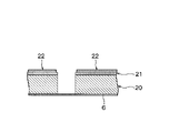
- FIG. 3 is an enlarged cross-sectional view of the semiconductor wafer shown in FIG. An enlarged cross-sectional view of a main part of a semiconductor wafer on which a protective film is formed.
- a perspective view showing a state in which a semiconductor wafer on which a protective film is formed is supported by an annular frame via a protective tape.
- the main part perspective view of the laser processing apparatus which carries out a laser beam irradiation process.
- FIG. 3 is an enlarged cross-sectional view of a semiconductor wafer including a protective film and a processing groove formed by laser irradiation.
- the protective film forming agent is used in dicing a semiconductor wafer to form a protective film on the surface of the semiconductor wafer.
- the protective film forming agent contains a water-soluble resin (A), an absorbent (B), and a solvent (S).
- the water-soluble resin (A) includes a water-soluble resin (A1).
- the water-soluble resin (A1) has an aromatic ring and a water-soluble group.
- the protective film is easy to remove by washing with water after processing the semiconductor wafer, and the protective film is sufficiently durable against plasma irradiation when plasma irradiation is performed in the semiconductor chip manufacturing method described later.
- the film thickness of is typically 0.1 ⁇ m or more and 100 ⁇ m or less, and more preferably 1 ⁇ m or more and 100 ⁇ m or less.
- the film thickness of the protective film is preferably 0.1 ⁇ m or more and 30 ⁇ m or less.
- the water-soluble resin (A) includes a water-soluble resin (A1) which is a water-soluble resin having an aromatic ring and a water-soluble group.
- the aromatic ring may be an aromatic hydrocarbon ring or an aromatic heterocycle. Further, the aromatic ring may have a monocyclic structure or a polycyclic structure.
- the polycyclic structure may be a polycyclic structure in which two or more monocycles are condensed, or a polycyclic structure in which two or more rings are bonded to each other via a single bond or a linking group. Examples of the aromatic ring having a monocyclic structure include a benzene ring. Examples of the aromatic ring having a polycyclic structure include a naphthalene ring, a biphenyl ring, an anthracene ring, and a phenanthrene ring.
- the water-soluble group is not particularly limited as long as it is a group capable of imparting water solubility to the resin.
- Examples of the water-soluble group include -SO 3 - X + (X + is an alkali metal cation, a proton, or N + R 4 ), and -COO - X + (X + is as described above. ), Hydroxyl group, or ether bond (-O-).
- X + is an alkali metal cation, a proton, or N + R 4
- -COO - X + X + is as described above.
- Hydroxyl group or ether bond
- R is a hydrogen atom, an alkyl group, or a hydroxyalkyl group.
- Examples of the alkali metal include sodium, potassium, strontium and the like.
- the protective film forming agent can form a processed groove having excellent straightness by laser irradiation, and has a fluorine shielding property. Can form an excellent protective film.
- the protective film forming agent by irradiating the protective film formed by using the above-mentioned protective film forming agent with a laser, it is possible to form a processed groove having excellent straightness.
- a plasma etching process on a machined groove having excellent straightness and dividing the wafer along the machined groove, a semiconductor chip having a cut surface having excellent straightness can be obtained.
- the protective film formed by using the above-mentioned protective film forming agent is excellent in fluorine shielding property. Therefore, when the protective film is formed by using the above-mentioned protective film forming agent, it is possible to suppress the fluorine contamination of the semiconductor substrate by the fluorine-based gas that occurs during the plasma etching process. On the other hand, when the protective film forming agent does not contain the water-soluble resin (A1), the protective film formed is inferior in straightness and fluorine shielding property of the processed groove formed by laser irradiation.
- Examples of the water-soluble resin (A1) include phenol resin and polystyrene resin.
- Examples of the phenol resin as the water-soluble resin (A1) include a resin having a structural unit represented by the following formula (1).
- R 31 is a water-soluble group.
- N 31 is an integer of 0 or more and 3 or less.
- the hydroxyl group When the hydroxyl group is a phenolic hydroxyl group, the hydroxyl group may form a salt such as an alkali metal salt.
- n31 is preferably 1.
- the substitution position of R 31 in the benzene ring may be any of the ortho-position, the meta-position, and the para-position with respect to the OH contained in the benzene ring.
- the phenol resin as the water-soluble resin (A1) include a phenol resin having a structural unit represented by the following formula (1-2), a structural unit represented by the following formula (1-1), and the following. Examples thereof include a phenol resin having a structural unit represented by the formula (1-2).
- a phenol resin having a structural unit represented by the formula (1-1) and a structural unit represented by the formula (1-2) the structural unit represented by the formula (1-1) and the structural unit (1-).
- the ratio of the number of moles of the structural unit represented by the formula (1-1) to the total number of moles of the structural unit represented by 2) is, for example, 0.1 to 0.9, and 0.7 to 0. 9 is preferable.
- X + is an alkali metal cation, a proton, or N + R 4
- R is a hydrogen atom, an alkyl group, or a hydroxyalkyl group.
- Examples of the polystyrene resin as the water-soluble resin (A1) include a resin having a structural unit represented by the following formula (2).
- R 32 is a water-soluble group.
- N 32 is an integer of 0 or more and 3 or less.
- X + is an alkali metal cation, a proton, or N + R4
- -COO - X + X + is as described above).
- Hydroxyl group, or ether bond (—O—).
- the hydroxyl group is a phenolic hydroxyl group
- the hydroxyl group may form a salt such as an alkali metal salt.
- n32 is preferably 1.
- the substitution position of R 32 on the benzene ring may be any of the ortho-position, the meta-position, and the para-position.
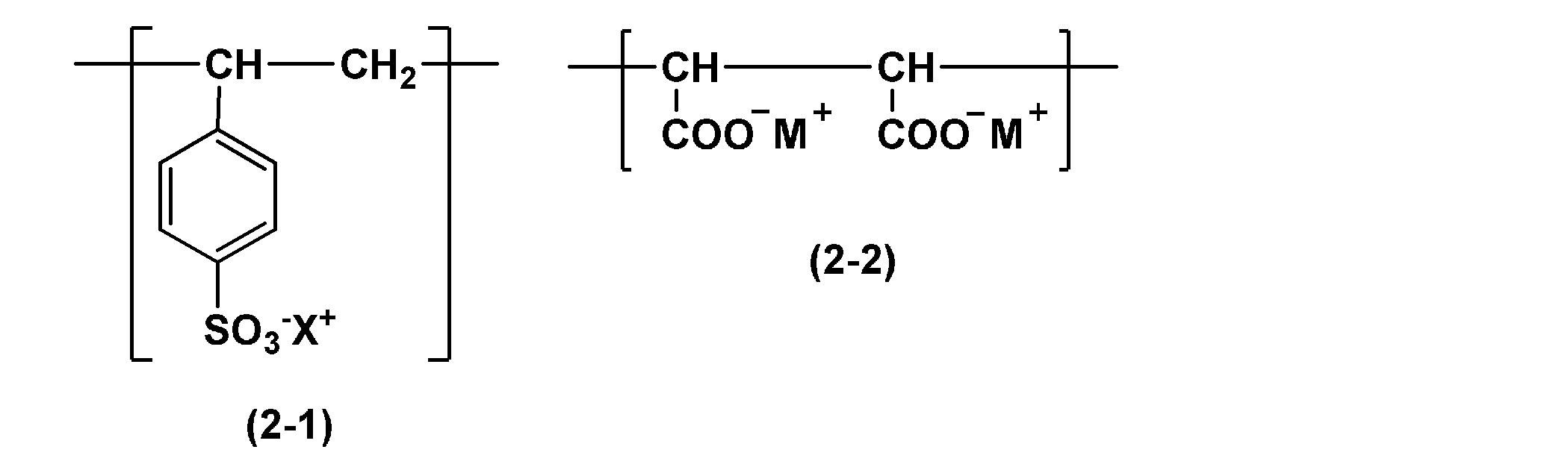
- polystyrene resin as the water-soluble resin (A1) include a polystyrene resin having a structural unit represented by the following formula (2-1), a structural unit represented by the following formula (2-1), and the following.
- examples thereof include polystyrene resins having a structural unit represented by the formula (2-2).
- X + is an alkali metal cation, a proton, or N + R 4
- R is a hydrogen atom, an alkyl group, or a hydroxyalkyl group.
- M + is an alkali metal cation, a proton, or N + R 014
- R 01 is a hydrogen atom, an alkyl group, or a hydroxyalkyl group.
- the alkali metal include sodium, potassium, strontium and the like.
- the mass average molecular weight of the water-soluble resin (A1) is preferably 15,000 or more and 300,000 or less, preferably 20,000 or more and 200, from the viewpoint of achieving both decomposability when irradiated with laser light and film forming property. More preferably, it is 000 or less.
- the mass average molecular weight is a polystyrene-equivalent molecular weight measured by GPC.
- the water-soluble resin (A) may be only the water-soluble resin (A1), but may contain a water-soluble resin other than the water-soluble resin (A1).
- a water-soluble resin other than the water-soluble resin (A1) is contained, the ratio of the mass of the water-soluble resin (A1) to the mass of the water-soluble resin (A) is, for example, 1% by mass or more and 90% by mass or less, and 1 It is preferably mass% or more and 70 mass% or less, and more preferably 1 mass% or more and 55 mass% or less.
- water-soluble resin other than the water-soluble resin (A1) examples include vinyl-based resin, cellulose-based resin, polyethylene oxide, polyglycerin, and water-soluble nylon. ..
- the vinyl-based resin is a homopolymer or copolymer of a monomer having a vinyl group, and is not particularly limited as long as it is a water-soluble resin.
- vinyl resins include polyvinyl alcohol, polyvinyl acetal (including vinyl acetate copolymer), polyvinylpyrrolidone, polyacrylamide, poly (N-alkylacrylamide), polyallylamine, poly (N-alkylallylamine), and partially amidated poly.
- the cellulosic resin is not particularly limited as long as it is a water-soluble cellulose derivative.
- Examples of the cellulosic resin include methyl cellulose, ethyl cellulose, hydroxypropyl cellulose and the like. These can be used alone or in combination of two or more.
- water-soluble resins vinyl-based resins and cellulose-based resins are preferable, and polyvinylpyrrolidone and hydroxypropyl cellulose are more preferable, because the shape of the processed groove is less likely to deteriorate due to heat sagging of the protective film. preferable. Further, from the viewpoint of film forming property, a cellulosic resin is preferable.
- the mass average molecular weight of other water-soluble resins is preferably 15,000 or more and 300,000 or less, preferably 20,000 or more and 200, More preferably, it is 000 or less.
- a water-soluble resin in the protective film forming agent (A) to the total mass of the mass of A) and the mass of the absorbent (B) is preferably 60% by mass or more and 99% by mass or less, and 80% by mass or more and 95% by mass or less. More preferred.
- an absorbent generally used as a protective film forming agent can be used.
- a water-soluble dye As the absorbent (B), it is preferable to use a water-soluble dye, a water-soluble dye, or a water-soluble absorbent such as a water-soluble ultraviolet absorber.
- the water-soluble absorbent is advantageous for uniformly present in the protective film.
- the water-soluble absorber include organic acids having a carboxy group or a sulfo group; sodium salts, potassium salts, ammonium salts, and quaternary ammonium salts of organic acids; compounds having a hydroxy group.
- the storage stability of the protective film-forming agent is high, and it is possible to suppress inconveniences such as phase separation of the protective film-forming agent and precipitation of the absorbent during storage of the protective film-forming agent. Therefore, it is also advantageous in that it is easy to maintain good coatability of the protective film forming agent for a long period of time.
- a water-insoluble absorbent such as a pigment can also be used.
- a water-insoluble absorbent When a water-insoluble absorbent is used, the use of the protective film-forming agent does not cause a fatal problem, but the laser absorption capacity of the protective film varies, and a protective film is formed having excellent storage stability and coatability. It may be difficult to obtain the agent or to form a protective film having a uniform thickness.
- Examples of the absorbent (B) include benzophenone compounds, cinnamic acid compounds, anthraquinone compounds, naphthalene compounds, and biphenyl compounds.
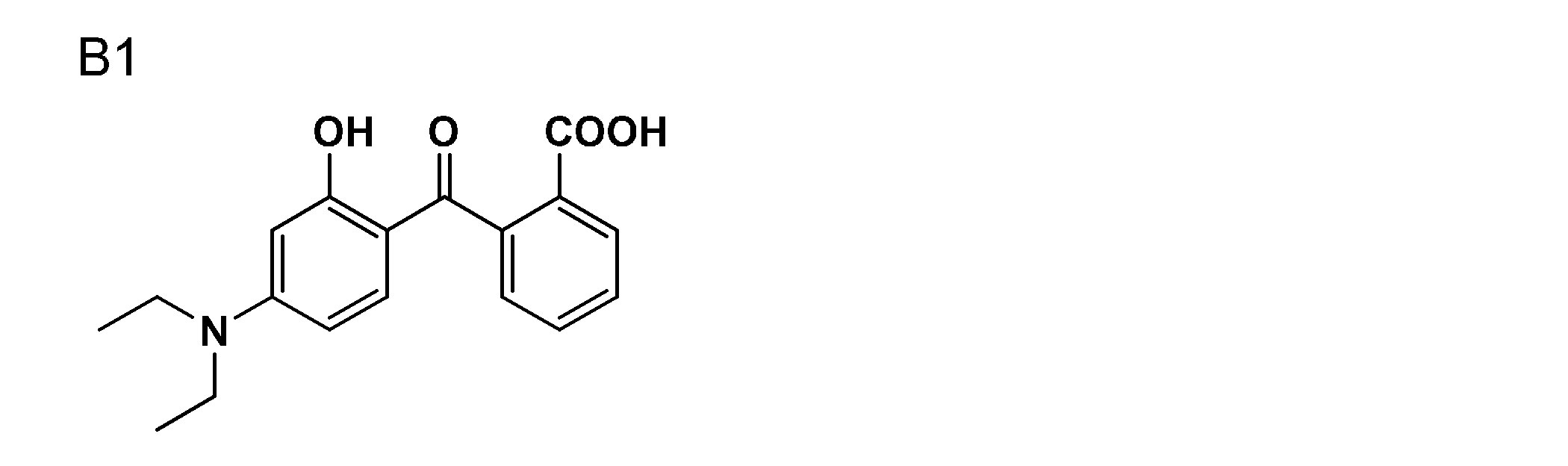
- Examples of the benzophenone compound include a compound represented by the following formula (B1).
- the compound represented by the following formula (B1) is preferable because the protective film can efficiently absorb the energy of the laser beam and promote the thermal decomposition of the protective film.
- R 1 and R 3 are independently represented by a hydroxyl group or a carboxy group
- R 2 and R 4 are independently represented by a hydroxyl group, a carboxy group, or -NR 5 R 6 .
- R 5 and R 6 are each independently a hydrogen atom or an alkyl group having 1 or more and 4 or less carbon atoms
- m and n are independently integers of 0 or more and 2 or less. .
- the compound represented by the above formula (B1) has a high absorption coefficient, and exhibits a high absorption coefficient even when added to a protective film forming agent together with an alkali. Therefore, when a protective film is formed using a protective film-forming agent containing the compound represented by the above formula (B1) as an absorbent (B), a partial laser of the protective film is formed when forming a mask for dicing. Can be satisfactorily decomposed by.
- R 2 and R 4 may be a group represented by ⁇ NR 5 R 6 .
- R 5 and R 6 are independently hydrogen atoms or alkyl groups having 1 or more and 4 or less carbon atoms.
- the alkyl groups as R 5 and R 6 may be linear or branched. Specific examples of the alkyl group as R 5 and R 6 are a methyl group, an ethyl group, an n-propyl group, an isopropyl group, an n-butyl group, an isobutyl group, a sec-butyl group, and a tert-butyl group.
- an amino group, a methylamino group, an ethylamino group, a dimethylamino group and a diethylamino group are preferable, and an amino group, a dimethylamino group and a diethylamino group are more preferable.
- the compound represented by the formula (B1) is preferably a compound represented by the following formula (B1-1) because of its high absorption coefficient in the presence of a base.
- Equations (in B1-1), R1 to R4 , m, and n are the same as those in equation (B1).)
- R 1 and R 3 are a hydroxyl group because of the high extinction coefficient in the presence of a base.
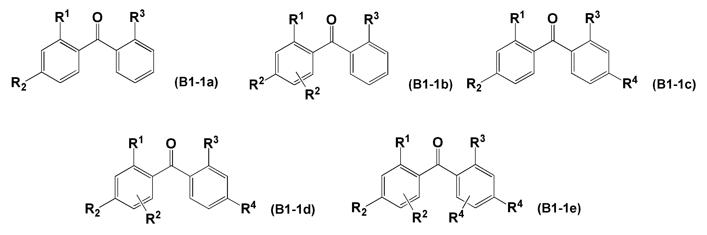
- the compound represented by the formula (B1-1) is preferably a compound represented by any of the following formulas (B1-1a) to (B1-1e). (In formulas (B1-1a) to (B1-1e), R1 to R4 are the same as those in formula (B1).)
- R 2 is the above-mentioned group represented by -NR 5 R 6 , and R 5 and R 6 are independent of each other. It is preferably an alkyl group having 1 or more and 4 or less carbon atoms.
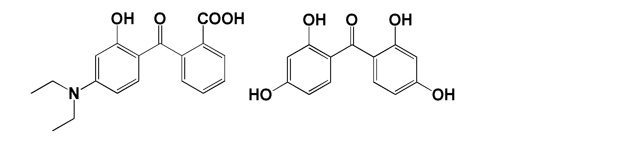
- Preferable specific examples of the compound represented by the formula (B1) include the following compounds. These compounds are preferable because they are easily available and exhibit a high extinction coefficient even in the presence of a base.
- the ratio of the mass of the compound represented by the formula (B1) to the mass of the absorbent (B) does not impair the object of the present invention.
- the range is not particularly limited.
- the ratio of the mass of the compound represented by the formula (B1) to the mass of the absorbent (B) is preferably 70% by mass or more, more preferably 80% by mass or more, further preferably 95% by mass or more, and 100% by mass. Is particularly preferable.
- benzophenone compound examples include 4,4'-dicarboxybenzophenone, benzophenone-4-carboxylic acid, and tetrahydroxybenzophenone. All of these are water-soluble UV absorbers.
- the alkoxy group as R 11 may be linear or branched.
- the alkoxy group as R 11 is preferably an alkoxy group having 1 or more and 4 or less carbon atoms. Specific examples of the alkoxy group as R 11 are a methoxy group, an ethoxy group, an n-propoxy group, an isopropoxy group, and an n-butoxy group.
- R 11 may be a group represented by ⁇ NR 12 R 13 .
- R 12 and R 13 are independently hydrogen atoms or alkyl groups having 1 or more and 4 or less carbon atoms.
- the alkyl groups as R 12 and R 13 may be linear or branched. Specific examples of the alkyl group as R 12 and R 13 are a methyl group, an ethyl group, an n-propyl group, an isopropyl group, an n-butyl group, an isobutyl group, a sec-butyl group, and a tert-butyl group.
- the compound represented by the formula (B2) is preferably a compound represented by the following formula (B2-1).
- R 11 is the same as R 11 in equation (B2).
- cinnamic acid-based compound examples include 4-aminocinnamic acid, 3-aminocinnamic acid, 2-aminocinnamic acid, sinapinic acid (3,5-dimethoxy-4-hydroxycinnamic acid), ferulic acid, and caffeic acid.
- 4-aminocinnamic acid, 3-aminocinnamic acid, 2-aminocinnamic acid, and ferulic acid are preferable, 4-aminocinnamic acid and ferulic acid are more preferable, and 4-aminocinnamic acid is particularly preferable.
- anthraquinone compound examples include 2-carboxyanthraquinone, 2,6-anthraquinone disulfonic acid, 2,7-anthraquinone disulfonic acid and the like.
- naphthalene compound examples include 1,2-naphthalindicarboxylic acid, 1,8-naphthalindicarboxylic acid, 2,3-naphthalindicarboxylic acid, 2,6-naphthalindicarboxylic acid, 2,7-naphthalindicarboxylic acid and the like. Can be mentioned.
- biphenyl compound examples include biphenyl-4-sulfonic acid and the like.
- absorbent (B) examples include curcumin and water-soluble amines such as EAB-F (4,4'-bis (diethylamino) benzophenone).
- water-soluble dyes include azo dyes (monoazo and polyazo dyes, metal complex salt azo dyes, pyrazolone azo dyes, stillben azo dyes, thiazole azo dyes), anthraquinone dyes (anthraquinone derivatives, anthron derivatives), and indigoid dyes (indigoid derivatives).
- azo dyes monoazo and polyazo dyes, metal complex salt azo dyes, pyrazolone azo dyes, stillben azo dyes, thiazole azo dyes
- anthraquinone dyes anthraquinone derivatives, anthron derivatives
- indigoid dyes indigoid derivatives
- a water-soluble dye is selected from among dyes, nitroso dyes, benzoquinone and naphthoquinone dyes, naphthalimide dyes, perinone dyes, and other dyes.
- water-soluble pigments examples include edible red No. 2, edible red No. 40, edible red No. 102, edible red No. 104, edible red No. 105, edible red No. 106, edible yellow NY, edible yellow No. 4 tartrazine, and edible yellow.
- Edible vermilion No. 101, edible blue No. 1, edible blue No. 2, edible green No. 3, edible melon color B, and edible egg color No. Dyes for food additives such as 3 are suitable because they have a low environmental load.
- the content of the light absorber (B) in the protective film forming agent is not particularly limited as long as it does not impair the object of the present invention.
- the content of the absorbent (B) in the protective film forming agent is preferably 0.1% by mass or more and 10% by mass or less.
- a water-soluble resin in the protective film forming agent ( The ratio of the mass of the light-absorbing agent (B) to the total mass of the mass of A) and the mass of the light-absorbing agent (B) is preferably 0.1% by mass or more and 50% by mass or less, and 1% by mass or more and 40% by mass or less. Is more preferable, and 2.5% by mass or more and 15% by mass or less is further preferable.
- the content of the absorbent (B) can be set so that the absorbance of the protective film formed by applying the protective film forming agent becomes a desired value.
- the absorbance of the protective film formed by applying the protective film forming agent is not particularly limited.
- the absorbance of the protective film formed by applying the protective film forming agent at a wavelength of 355 nm is 0. It is preferably .3 or more, more preferably 0.8 or more, and even more preferably 1.0 or more.
- the protective film forming agent may contain a basic compound (C) for the purpose of facilitating the dissolution of the compound represented by the formula (B1).
- a basic compound (C) for the purpose of facilitating the dissolution of the compound represented by the formula (B1).
- the basic compound (C) either an inorganic compound or an organic compound can be used.
- an organic compound is preferable.
- Specific examples of the basic compound (C) include basic inorganic compounds such as sodium hydroxide, potassium hydroxide, sodium carbonate, potassium carbonate, sodium silicate, sodium metasilicate, and ammonia, ethylamine, and n-propylamine.
- the amount of the basic compound (C) used is not particularly limited as long as it does not impair the object of the present invention.
- the amount of the basic compound (C) used is preferably 1 mol or more, more preferably 1 mol or more and 20 mol or less, based on 1 mol of the compound represented by the formula (B1).
- the lower limit of the amount of the basic compound (C) used may be 1.5 mol or more, 2 mol or more, and 3 mol or more with respect to 1 mol of the compound represented by the formula (B1). There may be.
- the upper limit of the amount of the basic compound (C) used may be 15 mol or less, 10 mol or less, and 5 mol or less with respect to 1 mol of the compound represented by the formula (B1). May be good.
- the protective film-forming agent may contain other compounding agents as long as the object of the present invention is not impaired.
- compounding agents for example, preservatives, surfactants and the like can be used.
- Preservatives include benzoic acid, butylparaben, ethylparaben, methylparaben, propylparaben, sodium benzoate, sodium propionate, benzalconium chloride, benzethonium chloride, benzyl alcohol, cetylpyridinium chloride, chlorobutanol, phenol, phenylethyl alcohol. , 2-Phenoxyethanol, phenylsecondary mercury nitrate, timerosal, metacresol, lauryldimethylamine oxide or a combination thereof can be used.
- the preservative not only from the viewpoint of preservative of the protective film forming agent but also from the viewpoint of reducing the load of processing the waste liquid after cleaning the semiconductor wafer.
- a large amount of cleaning water is generally used for cleaning semiconductor wafers.
- the waste liquid derived from the process using the protective film forming agent described above be treated separately from the waste liquid derived from the process not using the protective film forming agent.
- the protective film-forming agent contains an antiseptic
- the growth of various germs caused by the water-soluble resin (A) is suppressed, so that the waste liquid derived from the process using the protective film-forming agent and the protective film-forming agent Waste liquids derived from processes that do not use the above can be treated in the same manner. Therefore, the load on the wastewater treatment process can be reduced.
- the surfactant is used, for example, to improve the defoaming property during the production of the protective film forming agent, the stability of the protective film forming agent, the coatability of the protective film forming agent, and the like.
- a surfactant in terms of defoaming property during the production of the protective film forming agent.
- the protective film is formed by spin coating a protective film forming agent.
- a protective film forming agent such as a surfactant.
- a water-soluble surfactant can be preferably used.
- any of a nonionic surfactant, a cationic surfactant, an anionic surfactant, and an amphoteric surfactant can be used.
- the surfactant may be silicone-based. Nonionic surfactants are preferable from the viewpoint of detergency.
- the protective film forming agent usually contains a solvent (S) in order to dissolve the water-soluble resin (A) and the absorbent (B).
- a solvent (S) any of water, an organic solvent, and an aqueous solution of an organic solvent can be used.
- water and an aqueous solution of an organic solvent are preferable, and water is more preferable, from the viewpoint of less risk of ignition during use and cost.
- the content of the organic solvent in the solvent (S) is preferably 30% by mass or less, more preferably 20% by mass or less, and further preferably 15% by mass or less.
- the solvent (S) is preferably selected so that the protective film forming agent does not have a flash point under 1 atm. Specifically, by adjusting the water content in the protective film forming agent, the flash point of the protective film and the presence or absence of the flash point are adjusted.
- Protective film-forming agents that do not have a flash point are safe and can be placed, for example, in a non-explosion-proof environment. Specifically, the protective film forming agent can be stored, transported, used, etc. in a non-explosion-proof environment. For example, not only the protective film forming agent can be introduced into a semiconductor factory, but also the protective film can be formed in a non-explosion-proof environment. Therefore, a protective film forming agent having no flash point is industrially very advantageous in that an explosion-proof environment such as an explosion-proof facility, which is usually expensive, is not required.
- the flash point is obtained by measuring with a tag closed type when the liquid temperature is 80 ° C. or lower and by using the Cleveland open type when the liquid temperature exceeds 80 ° C. under 1 atm. In the specification of the present application and the scope of claims, if the flash point cannot be measured even if the measurement is performed by the Cleveland open method, the flash point is defined as no flash point.
- Examples of the organic solvent that can be contained in the protective film forming agent include methyl alcohol, ethyl alcohol, alkylene glycol, alkylene glycol monoalkyl ether, alkylene glycol monoalkyl ether acetate and the like.
- Examples of the alkylene glycol include ethylene glycol and propylene glycol.
- Examples of the alkylene glycol monoalkyl ether include ethylene glycol monomethyl ether, ethylene glycol monoethyl ether, propylene glycol monomethyl ether, and propylene glycol monoethyl ether.
- alkylene glycol monoalkyl ether acetate examples include ethylene glycol monomethyl ether acetate, ethylene glycol monoethyl ether acetate, propylene glycol monomethyl ether acetate, and propylene glycol monoethyl ether acetate.
- the protective film forming agent may contain a combination of two or more kinds of organic solvents.
- the solid content concentration of the protective film forming agent is not particularly limited as long as the object of the present invention is not impaired.
- the solid content concentration is, for example, preferably 5% by mass or more and 60% by mass or less, and more preferably 10% by mass or more and 50% by mass or less.
- the method for manufacturing a semiconductor chip is a method including processing a semiconductor wafer to manufacture a semiconductor chip. More specifically, the method for manufacturing a semiconductor chip is as follows. To form a protective film by applying the above-mentioned protective film forming agent on a semiconductor wafer, By irradiating a predetermined position of one or more layers including a protective film on a semiconductor wafer with laser light, the surface of the semiconductor wafer is exposed and a processing groove having a pattern corresponding to the shape of the semiconductor chip is formed. It is a method including.
- the semiconductor chip manufacturing method described above comprises a cutting step of cutting a street position on a semiconductor wafer.
- forming a protective film is also referred to as a "protective film forming step”
- forming a machined groove is also referred to as a “working groove forming step”
- cutting a street position on a semiconductor wafer is also referred to as a “cutting step”. I will write it.
- the protective film forming agent described above is applied onto the semiconductor wafer to form the protective film.
- the shape of the processed surface of the semiconductor wafer is not particularly limited as long as the desired processing can be applied to the semiconductor wafer.
- the machined surface of a semiconductor wafer has a large number of irregularities.
- a recess is formed in the area corresponding to the street.
- On the processed surface of the semiconductor wafer a plurality of regions corresponding to semiconductor chips are partitioned by streets.
- the film thickness of the protective film is typical in terms of easy removal of the protective film by washing with water after processing and sufficient durability of the protective film against plasma irradiation when plasma irradiation is performed in the cutting step described later. Is preferably 0.1 ⁇ m or more and 100 ⁇ m or less, and more preferably 1 ⁇ m or more and 100 ⁇ m or less.
- the film thickness of the protective film is preferably 0.1 ⁇ m or more and 30 ⁇ m or less.
- a semiconductor chip will be described with respect to a method for manufacturing a semiconductor chip in which a semiconductor wafer including a plurality of semiconductor chips partitioned by grid-like streets is diced using the above-mentioned protective film agent. This will be described as a preferred embodiment of the method for producing the above.
- FIG. 1 shows a perspective view of a semiconductor wafer to be processed.
- FIG. 2 shows an enlarged cross-sectional view of a main part of the semiconductor wafer shown in FIG.
- a laminate 21 in which a functional film forming an insulating film and a circuit is laminated is provided on the surface 20a of a semiconductor substrate 20 such as silicon.
- a plurality of semiconductor chips 22 such as ICs and LSIs are formed in a matrix.
- the shape and size of the semiconductor chip 22 are not particularly limited, and can be appropriately set according to the design of the semiconductor chip 22.
- the insulating film used as the laminate 21 is a SiO 2 film, an inorganic film such as SiOF or BSG (SiOB), or a polymer film such as polyimide or parylene. It is composed of a low dielectric constant insulator film (Low-k film) composed of a certain organic film.
- the surface of the laminated body 21 corresponds to the surface 2a which is a processed surface.
- a protective film is formed on the surface 2a by using the protective film forming agent described above.
- a protective film forming agent is applied to the surface 2a of the semiconductor wafer 2 by a spin coater to form a protective film.
- the method of applying the protective film forming agent is not particularly limited as long as a protective film having a desired film thickness can be formed.
- the liquid protective film forming agent that coats the surface 2a is dried.
- the protective film 24 is formed on the surface 2a on the semiconductor wafer 2 as shown in FIG.
- the protective tape 6 attached to the annular frame 5 is attached to the back surface of the semiconductor wafer 2 as shown in FIG. To.
- ⁇ Processing groove formation process> laser light is irradiated to a predetermined position of one or more layers including the protective film 24 on the semiconductor wafer 2, the surface 20a of the semiconductor substrate 20 is exposed, and the shape of the semiconductor chip 22 is adjusted. A machined groove of the pattern is formed.
- the surface 2a (street 23) on the semiconductor wafer 2 is irradiated with laser light through the protective film 24.
- the irradiation of the laser light is carried out by using the laser beam irradiating means 72 as shown in FIG.
- the laser is preferably an ultraviolet laser having a wavelength of 100 nm or more and 400 nm or less.
- a YVO4 laser having a wavelength of 266 nm and 355 nm and the like, and a YAG laser are preferable.
- the laser light irradiation in the processing groove forming step is performed under the following processing conditions, for example.
- the diameter of the condensing spot is appropriately selected in consideration of the width of the processing groove 25.
- Laser light source YVO4 laser or YAG laser Wavelength: 355 nm Repeat frequency: 50 kHz or more and 100 kHz or less Output: 0.3 W or more and 4.0 W or less Processing feed rate: 1 mm / sec or more and 800 mm / sec or less
- the processing groove 25 is formed along the street 23 in the laminated body 21 including the street 23 in the semiconductor wafer 2.
- the protective film 24 is formed by the above-mentioned protective film forming agent containing a water-soluble resin (A1) having an aromatic ring and a water-soluble group, the protective film 24 is irradiated with laser light as described above.
- a groove (processed groove 25) having a cross section excellent in straightness can be formed in the protective film 24.
- the semiconductor wafer 2 held by the chuck table 71 is indexed and moved in the direction indicated by the arrow Y by the distance of the street, and the laser beam is irradiated again. To carry out.
- the semiconductor wafer 2 held on the chuck table 71 is rotated by 90 degrees to rotate the semiconductor wafer 2 in the predetermined direction by 90 degrees.
- laser light irradiation and indexing movement are performed in the same manner as described above. In this way, the machined grooves 25 can be formed along all the streets 23 formed in the laminated body 21 on the semiconductor wafer 2.
- a preferred method is a method of cutting the semiconductor wafer 2 by irradiating the semiconductor wafer 2 provided with the protective film 24 and the processing groove 25 with plasma.
- the plasma is irradiated to a part or the entire surface of the semiconductor wafer 2 provided with the protective film so that the plasma is exposed to the surface of the processing groove 25.
- a cutting method by plasma irradiation will be described.
- the semiconductor wafer 2 provided with the protective film 24 and the processing groove 25 is irradiated with plasma.
- the position of the processing groove 25 in the semiconductor wafer 2 is cut as shown in FIG. Specifically, in the semiconductor wafer 2 coated with the protective film 24, as described above, after forming the processing groove 25, the protective film 24 and the surface 20a of the semiconductor substrate 20 exposed from the processing groove 25 are exposed to each other.
- the semiconductor wafer 2 is cut according to the shape of the semiconductor chip 22, and the semiconductor wafer 2 is divided into the semiconductor chips 22.
- the plasma irradiation conditions are not particularly limited as long as the semiconductor wafer 2 can be cut well at the position of the processing groove 25.
- the plasma irradiation conditions are appropriately set within the range of general conditions for plasma etching of the semiconductor substrate 20 in consideration of the material of the semiconductor wafer 2, the plasma type, and the like.
- the gas used to generate plasma in plasma irradiation is appropriately selected depending on the material of the semiconductor wafer 2. Typically, SF 6 gas is used to generate the plasma.
- SF 6 gas is used to generate the plasma.
- BOSCH process etching with a high aspect ratio is possible, and even when the semiconductor wafer 2 is thick, the semiconductor wafer 2 can be easily cut.
- a fluorine-based gas is generally used for plasma irradiation. Therefore, there is a problem that the semiconductor substrate 20 may be contaminated by fluorine that has passed through the protective film during the plasma etching process.
- the protective film 24 is formed by the above-mentioned protective film forming agent containing a water-soluble resin (A1) having an aromatic ring and a water-soluble group, the protective film 24 is excellent in fluorine shielding property. Therefore, it is possible to suppress the permeation of the fluorine-based gas through the protective film during plasma irradiation, and the contamination of the semiconductor substrate by fluorine is suppressed.
- the protective film 24 is formed by the above-mentioned protective film forming agent containing a water-soluble resin (A1) having an aromatic ring and a water-soluble group
- the processed groove 25 has a cross section excellent in straightness. Therefore, a semiconductor chip having excellent straightness can be obtained by plasma irradiation.
- the protective film 24 covering the surface of the semiconductor chip 22 is removed.
- the protective film 24 is formed by using the protective film forming agent containing the water-soluble resin (A)
- the protective film 24 can be washed away with water (or warm water).
- the protective film 24 is excellent in fluorine shielding property. Therefore, by washing away the protective film 24, a semiconductor chip in which the amount of fluorine is suppressed can be obtained.
- the method of manufacturing a semiconductor chip by processing a semiconductor wafer has been described above based on the embodiment.
- the protective film forming agent according to the present invention and the method for manufacturing a semiconductor chip are such that a protective film is formed on the surface of a semiconductor wafer and a processing groove is formed at a position corresponding to a street on the surface of the semiconductor wafer provided with the protective film. Any method including the above can be applied to various semiconductor chip manufacturing methods.
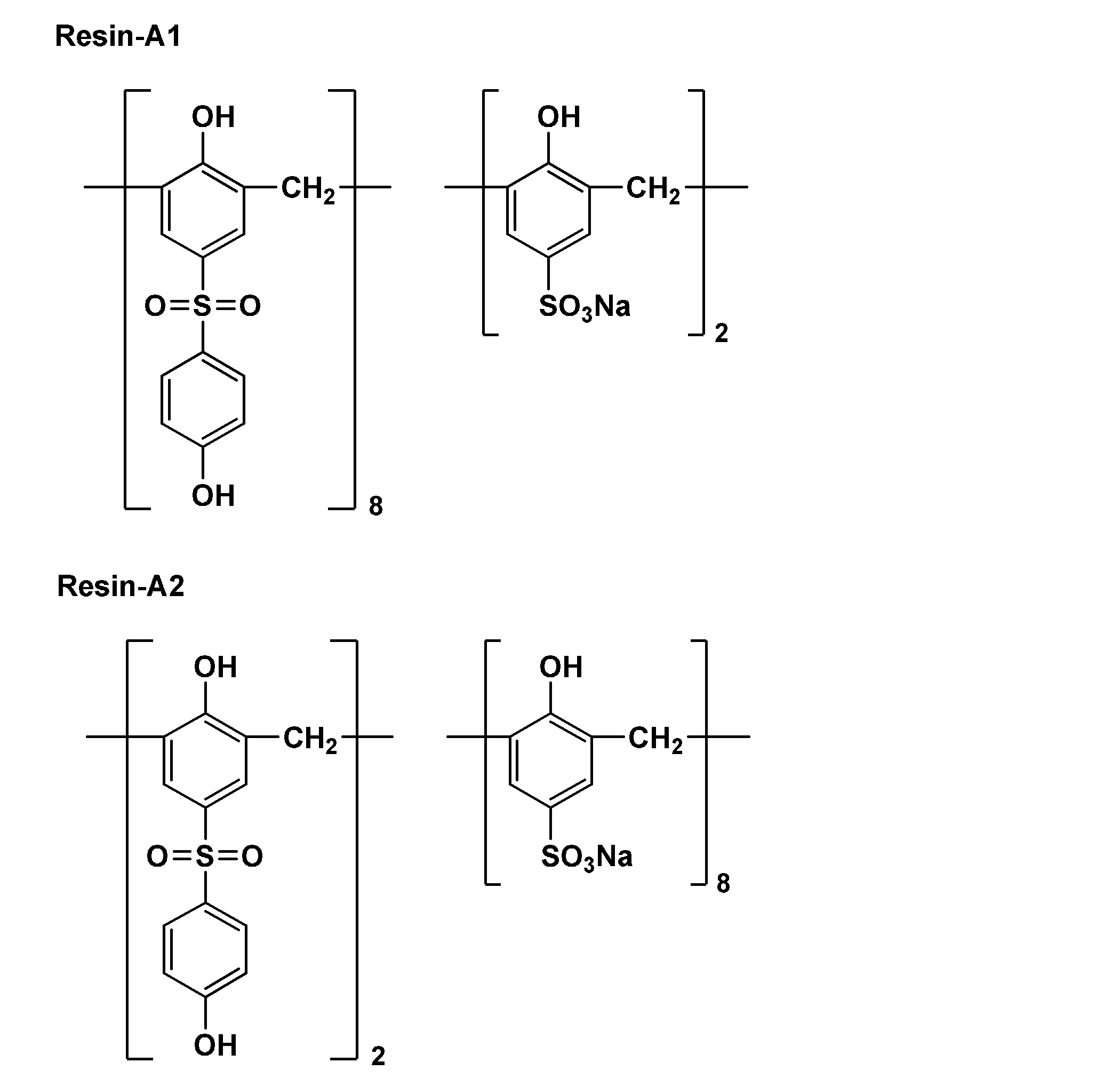
- Example 1 to 16 and Comparative Examples 1 to 4 In Examples and Comparative Examples, as the water-soluble resin (A), the following Resin-A1 to Resin-A8 as the water-soluble resin (A1) having an aromatic ring and a water-soluble group, and Resin-A9 as the cellulosic resin. And Resin-A10 as a vinyl resin was used.
- the numbers in the lower right of the parentheses in each structural unit in the following structural formula represent the molar ratio of the structural units in each resin.
- Resin-A1 is WSR-SP82 manufactured by Konishi Chemical Industry Co., Ltd., and has a mass average molecular weight of 22000.
- Resin-A2 is WSR-SP28 manufactured by Konishi Chemical Industry Co., Ltd., and has a mass average molecular weight of 20000.
- Resin-A3 is a neutralized sodium hydroxide (pH 8.8) of PSA-R manufactured by Konishi Chemical Industry Co., Ltd., and has a mass average molecular weight of 21000.
- Resin-A4 is an ammonia neutralized product (pH 8.6) of PSA-R manufactured by Konishi Chemical Industry Co., Ltd., and has a mass average molecular weight of 21000.
- Resin-A5 is a neutralized sodium hydroxide (pH 7.2) of VERSA-TL 72 manufactured by AkzoNobel, and has a mass average molecular weight of 75,000.
- Resin-A6 is an ammonia neutralized product (pH 7.2) of VERSA-TL 72 manufactured by AkzoNobel, and has a mass average molecular weight of 75,000.
- Resin-A7 is VERSA-TL 125 manufactured by AkzoNobel, and has a mass average molecular weight of 200,000.
- Resin-A8 is NARLEX D72 manufactured by AkzoNobel, and has a mass average molecular weight of 20000.
- Resin-A9 is HPC-SSL (hydroxypropyl cellulose) manufactured by Nippon Soda Corporation, and has a mass average molecular weight of 40,000.
- Resin-A10 is Pittscol K-90 (polyvinylpyrrolidone) manufactured by Dai-ichi Kogyo Seiyaku Co., Ltd., and has a mass average molecular weight of 1200000.
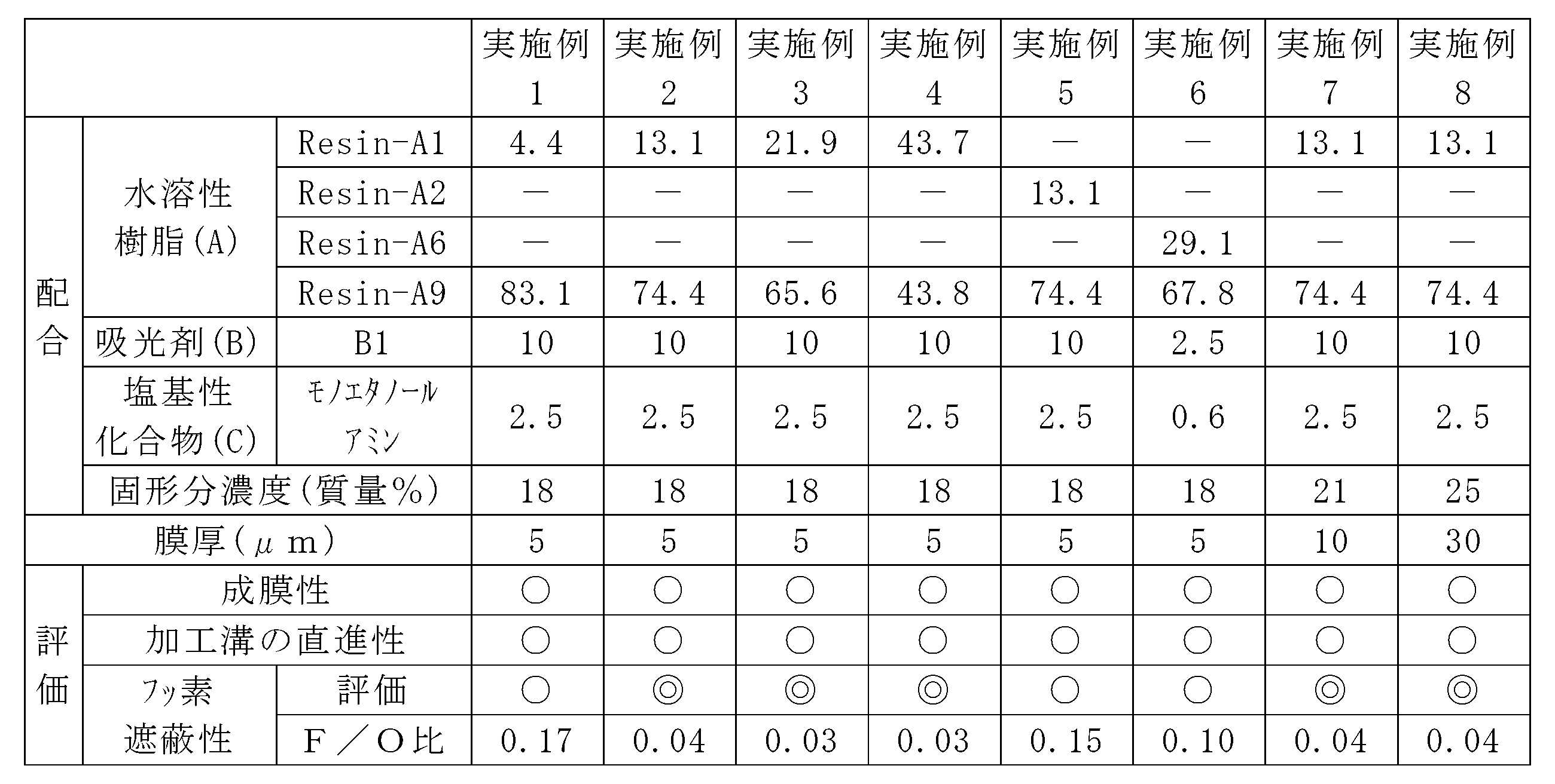
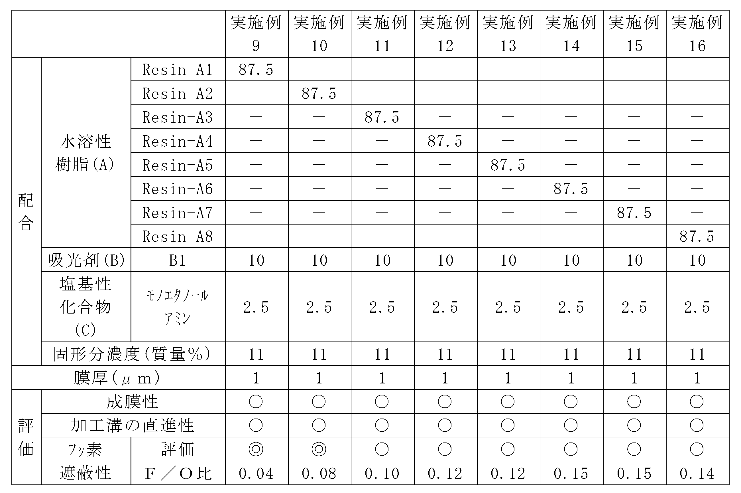
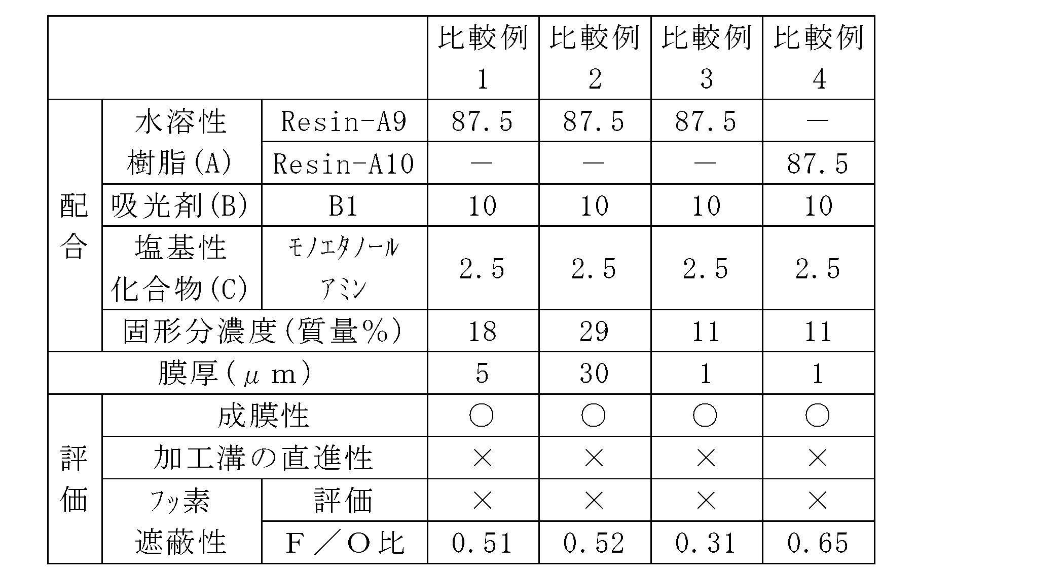
- the monoethanolamine as the basic compound (C) and the solvent (S) were put into a container so as to have the solid mass concentration shown in Tables 1 to 3 and stirred for 3 hours in each example. And a protective film-forming agent of Comparative Example was obtained.
- the solid content concentration is the total mass of the water-soluble resin (A), the absorbent (B) and the basic compound (C), and the water-soluble resin (A), the absorbent (B) and the basic compound (C).
- the solvent (S) a mixed solvent of 85 parts by mass of water and 15 parts by mass of propylene glycol monomethyl ether was used.
- the obtained protective film forming agent was applied onto a silicon substrate by a spin coating method so as to have the film thicknesses shown in Tables 1 to 3 to form a protective film.
- the surface of the silicon substrate provided with the protective film on the protective film side is linearly irradiated with a laser under the following conditions, and the cross-sectional shape of the laser-irradiated portion of the protective film is observed by an SEM (scanning electron microscope). , Evaluated according to the evaluation criteria described later. The results are shown in Tables 1 to 3.
- the obtained protective film forming agent was applied onto an aluminum substrate by a spin coating method so as to have the film thicknesses shown in Tables 1 to 3 to form a protective film.
- the surface of the aluminum substrate provided with the protective film on the protective film side is linearly irradiated with a laser under the same laser irradiation conditions as in the above [evaluation of straightness (laser workability) of the machined groove] to form the machined groove. Formed. Then, after plasma irradiation, the protective film was removed by washing with water. In plasma irradiation, plasma of SF 6 gas and C 4 F 8 gas was alternately irradiated for 100 cycles in the BOSCH process.
- the surface of the washed aluminum substrate is analyzed by X-ray Photoelectron Spectroscopy (XPS), and when the value of fluorine atom / oxygen atom (F / O ratio) is less than 0.10, ⁇ , The fluorine shielding property was evaluated as ⁇ when the F / O ratio was 0.10 or more and less than 0.20, and x when the F / O ratio was 0.20 or more.
- XPS X-ray Photoelectron Spectroscopy
- the protective film formed by using the protective film forming agent containing the water-soluble resin (A1) in which the protective film 24 has an aromatic ring and a water-soluble group is excellent in straightness by laser. It can be seen that the processed groove can be formed and the fluorine shielding property is excellent.
Landscapes
- Engineering & Computer Science (AREA)
- Physics & Mathematics (AREA)
- Optics & Photonics (AREA)
- Chemical & Material Sciences (AREA)
- Plasma & Fusion (AREA)
- Mechanical Engineering (AREA)
- Life Sciences & Earth Sciences (AREA)
- Materials Engineering (AREA)
- Wood Science & Technology (AREA)
- Organic Chemistry (AREA)
- Dicing (AREA)
- Electromagnetism (AREA)
Abstract
Description
しかしながら、特許文献1に記載された水溶性材料等の従来の水溶性材料を用いてマスクとしての保護膜を形成する場合、形成される加工溝の直進性が悪い、すなわち、加工溝を構成する保護膜の側壁の直進性が悪い場合があるという問題がある。加工溝の直進性が悪いと、半導体基板のプラズマエッチング等により切断して得られる半導体チップの直進性が悪くなる。
水溶性樹脂(A)と、吸光剤(B)と、溶媒(S)とを含み、
水溶性樹脂(A)が、水溶性樹脂(A1)を含み、
水溶性樹脂(A1)が、芳香環と、水溶性基とを有する、保護膜形成剤である。
半導体ウエハー上に、第1の態様にかかる保護膜形成剤を塗布して保護膜を形成することと、
半導体ウエハー上における保護膜を含む1以上の層の所定の位置にレーザー光を照射し、半導体ウエハーの表面が露出し、且つ半導体チップの形状に応じたパターンの加工溝を形成することと、
を含む、半導体チップの製造方法である。
保護膜形成剤は、半導体ウエハーのダイシングにおいて、半導体ウエハーの表面に保護膜を形成するために用いられる。保護膜形成剤は、水溶性樹脂(A)と、吸光剤(B)と、溶媒(S)とを含む。水溶性樹脂(A)は、水溶性樹脂(A1)を含む。水溶性樹脂(A1)は、芳香環と、水溶性基とを有する。
上記の保護膜と、上記の加工溝とを備える半導体ウエハーにプラズマを照射して、半導体ウエハーにおける加工溝の位置を加工することと、
を含む半導体チップの製造方法における、保護膜の形成に好適に用いられる。
レーザーを照射する場合、保護膜の膜厚は、0.1μm以上30μm以下が好ましい。
水溶性樹脂(A)は、保護膜形成剤を用いて形成される保護膜の基材である。水溶性樹脂(A)は、水等の溶媒に溶解させて塗布・乾燥して膜を形成し得る樹脂である。
水溶性とは、25℃の水100gに対して、溶質(水溶性樹脂)が0.5g以上溶解することをいう。
芳香環は、芳香族炭化水素環でも芳香族複素環でもよい。
また、芳香環は、単環構造であっても、多環構造であってもよい。多環構造は、2以上の単環が縮合した多環構造であっても、2以上の環が単結合又は連結基を介して互いに結合した多環構造であってもよい。
単環構造の芳香環としては、ベンゼン環が挙げられる。
多環構造の芳香環としては、ナフタレン環、ビフェニル環、アントラセン環、フェナントレン環が挙げられる。
このように、上述の保護膜形成剤を用いて形成された保護膜に対してレーザー照射を行うことにより直進性に優れた加工溝を形成できる。直進性に優れた加工溝に対してプラズマエッチング処理を行い、加工溝に沿ってウエハーを分割すると、直進性に優れた切断面を有する半導体チップを得ることができる。
また、上述の保護膜形成剤を用いて形成された保護膜は、フッ素遮蔽性に優れる。このため、上述の保護膜形成剤を用いて保護膜を形成する場合、プラズマエッチング処理時に生じる、フッ素系ガスによる半導体基板のフッ素汚染が抑制できる。
他方、保護膜形成剤が水溶性樹脂(A1)を含まない場合は、形成される保護膜は、レーザー照射により形成される加工溝の直進性やフッ素遮蔽性に劣る。
水溶性樹脂(A1)としてのフェノール樹脂としては、下記式(1)で表される構成単位を有する樹脂が挙げられる。

水溶性基としては、上述のとおり、-SO3 -X+(X+は、アルカリ金属カチオン、プロトン、又はN+R4である。)、-COO-X+(X+は前述の通りである。)、水酸基、又はエーテル結合(-O-)が挙げられる。水酸基がフェノール性水酸基である場合、当該水酸基はアルカリ金属塩等の塩を形成していてもよい。
n31は1であることが好ましい。ベンゼン環におけるR31の置換位置は、ベンゼン環が有するOHに対して、オルト位、メタ位、パラ位のいずれでもよい。


水溶性基としては、上述のとおり、-SO3 -X+(X+は、アルカリ金属カチオン、プロトン、又はN+R4である。)、-COO-X+(X+は前述の通りである。)、水酸基、又はエーテル結合(-O-)が挙げられる。水酸基がフェノール性水酸基である場合、当該水酸基はアルカリ金属塩等の塩を形成していてもよい。
n32は1であることが好ましい。ベンゼン環におけるR32の置換位置は、オルト位、メタ位、パラ位のいずれでもよい。
M+は、アルカリ金属カチオン、プロトン、又はN+R01 4であり、R01は、水素原子、アルキル基、又はヒドロキシアルキル基である。
アルカリ金属としては、ナトリウム、カリウム、ストロンチウム等が挙げられる。)
また、保護膜形成剤の全固形分中における、水溶性樹脂(A1)の含有量は、フッ素遮蔽性の観点から、10質量%以上99質量%以下であることが好ましく、10質量%以上50質量%以下であることがより好ましい。
水溶性樹脂(A1)以外の水溶性樹脂(以下「その他の水溶性樹脂」ともいう)としては、ビニル系樹脂、セルロース系樹脂、ポリエチレンオキサイド、ポリグリセリン、及び水溶性ナイロン等を挙げることができる。
ビニル系樹脂としては、ビニル基を有する単量体の単独重合体、又は共重合体であって、水溶性の樹脂であれば特に限定されない。ビニル系樹脂としては、ポリビニルアルコール、ポリビニルアセタール(酢酸ビニル共重合体も含む)、ポリビニルピロリドン、ポリアクリルアミド、ポリ(N-アルキルアクリルアミド)、ポリアリルアミン、ポリ(N-アルキルアリルアミン)、部分アミド化ポリアリルアミン、ポリ(ジアリルアミン)、アリルアミン・ジアリルアミン共重合体、ポリアクリル酸、ポリビニルアルコールポリアクリル酸ブロック共重合体、及びポリビニルアルコールポリアクリル酸エステルブロック共重合体が挙げられる。
セルロース系樹脂としては、水溶性のセルロース誘導体であれば特に限定されない。セルロース系樹脂としては、メチルセルロース、エチルセルロース、及びヒドロキシプロピルセルロース等が挙げられる。
これらは、1種単独で使用することもできるし、2種以上を組み合わせて使用することもできる。
また、成膜性の観点から、セルロース系樹脂が好ましい。
吸光剤(B)としては、一般的に保護膜形成剤に使用されている吸光剤を使用することができる。
吸光剤(B)として、水溶性染料、水溶性色素や、水溶性紫外線吸収剤等の水溶性吸光剤を使用することが好ましい。水溶性吸光剤は、保護膜中に均一に存在させる上で有利である。水溶性吸光剤としては、カルボキシ基やスルホ基を有する有機酸類;有機酸類のナトリウム塩、カリウム塩、アンモニウム塩、及び第4級アンモニウム塩;ヒドロキシ基を有する化合物を挙げることができる。
水溶性の吸光剤を用いる場合、保護膜形成剤の保存安定性が高く、保護膜形成剤の保存中に、保護膜形成剤の相分離や吸光剤の沈降等の不都合を生じることが抑制されるため、保護膜形成剤の良好な塗布性を長期間維持しやすい点でも有利である。
ベンゾフェノン系化合物としては、下記式(B1)で表される化合物が挙げられる。下記式(B1)で表される化合物は、保護膜にレーザー光のエネルギーを効率よく吸収させ、保護膜の熱分解を促進させることができるため、好ましい。


式(B1-1a)~式(B1-1e)で表される化合物において、R2が、-NR5R6で表される前述の基であって、R5及びR6が、それぞれ独立に炭素原子数1以上4以下のアルキル基であるのが好ましい。
これらの化合物は、入手の容易性や、塩基の存在下でも高い吸光係数を示すことから、好ましい。


これらの中でも、4-アミノ桂皮酸、3-アミノ桂皮酸、2-アミノ桂皮酸、及びフェルラ酸が好ましく、4-アミノ桂皮酸、及びフェルラ酸がより好ましく、4-アミノ桂皮酸が特に好ましい。
保護膜に対してレーザー光を照射して加工溝を形成する際の開口不良や、保護膜の熱ダレによる加工溝の形状悪化等が生じにくいことから、保護膜形成剤における、水溶性樹脂(A)の質量と、吸光剤(B)の質量との総量に対する、吸光剤(B)の質量の比率は、0.1質量%以上50質量%以下が好ましく、1質量%以上40質量%以下がより好ましく、2.5質量%以上15質量%以下がさらに好ましい。
吸光剤(B)の含有量は、保護膜形成剤を塗布して形成される保護膜の吸光度が所望の値になるように設定できる。保護膜形成剤を塗布して形成される保護膜の吸光度は特に限定されないが、例えば、保護膜形成剤を塗布して形成される保護膜の波長355nmでの膜厚1μmあたりの吸光度が、0.3以上であることが好ましく、0.8以上であることがより好ましく、1.0以上であることがさらに好ましい。
保護膜形成剤は、式(B1)で表される化合物を溶解させやすくする目的で塩基性化合物(C)を含んでいてもよい。塩基性化合物(C)としては、無機化合物、及び有機化合物のいずれも使用できる。塩基性化合(C)としては、有機化合物が好ましい。
塩基性化合物(C)の具体例としては、水酸化ナトリウム、水酸化カリウム、炭酸ナトリウム、炭酸カリウム、ケイ酸ナトリウム、メタケイ酸ナトリウム、及びアンモニア等の塩基性無機化合物や、エチルアミン、n-プロピルアミン、モノエタノールアミン、ジエチルアミン、ジ-n-プロピルアミン、ジエタノールアミン、トリエチルアミン、メチルジエチルアミン、ジメチルエタノールアミン、トリエタノールアミン、テトラメチルアンモニウムヒドロキシド、テトラエチルアンモニウムヒドロキシド、ピロール、ピペリジン、1,8-ジアザビシクロ[5,4,0]-7-ウンデセン、及び1,5-ジアザビシクロ[4,3,0]-5-ノナン等の塩基性有機化合物が挙げられる。
保護膜形成剤は、水溶性樹脂(A)、及び吸光剤(B)以外にも、本発明の目的を阻害しない限りにおいて、他の配合剤を含んでいてもよい。他の配合剤としては、例えば、防腐剤、及び界面活性剤等を用いることができる。
保護膜形成剤は、通常、水溶性樹脂(A)や吸光剤(B)を溶解させるために、溶媒(S)を含む。溶媒(S)としては、水、有機溶媒、及び有機溶媒の水溶液のいずれも用いることができる。使用時の引火等の危険が少ないことや、コストの点等で、溶媒(S)としては、水、及び有機溶媒の水溶液が好ましく、水がより好ましい。
引火点をもたない保護膜形成剤は安全であり、例えば、非防爆環境下に置くことができる。具体的には、保護膜形成剤の保管、輸送、使用等の取扱いを非防爆環境下に行うことができる。例えば、保護膜形成剤の半導体工場への導入のみならず、保護膜の形成を非防爆環境下に行うことができる。従って、通常高価な防爆設備等の防爆環境が不要である点で、引火点をもたない保護膜形成剤は、産業上非常に有利である。
本出願の明細書及び特許請求の範囲においては、クリーブランド開放式で測定しても、引火点が測定できなかった場合を、引火点なしとする。
アルキレングリコールとしては、エチレングリコール、及びプロピレングリコール等が挙げられる。アルキレングリコールモノアルキルエーテルとしては、エチレングリコールモノメチルエーテル、エチレングリコールモノエチルエーテル、プロピレングリコールモノメチルエーテル、及びプロピレングリコールモノエチルエーテル等が挙げられる。アルキレングリコールモノアルキルエーテルアセテートとしては、エチレングリコールモノメチルエーテルアセテート、エチレングリコールモノエチルエーテルアセテート、プロピレングリコールモノメチルエーテルアセテート、及びプロピレングリコールモノエチルエーテルアセテート等が挙げられる。
保護膜形成剤は、2種以上の有機溶媒を組み合わせて含んでいてもよい。
半導体チップの製造方法は、半導体ウエハーを加工して半導体チップを製造することを含む方法である。
より具体的には、半導体チップの製造方法は、
半導体ウエハー上に、前述の保護膜形成剤を塗布して保護膜を形成することと、
半導体ウエハー上における保護膜を含む1以上の層の所定の位置にレーザー光を照射し、半導体ウエハーの表面が露出し、且つ半導体チップの形状に応じたパターンの加工溝を形成することと、
を含む方法である。
典型的には、上記の半導体チップの製造方法は、半導体ウエハーにおけるストリートの位置を切断する切断工程を含む。
以下、保護膜を形成することについて「保護膜形成工程」とも記し、加工溝を形成することについて「加工溝形成工程」とも記し、半導体ウエハーにおけるストリートの位置を切断することについて「切断工程」とも記す。
保護膜形成工程では、半導体ウエハー上に、前述の保護膜形成剤を塗布して保護膜が形成される。
半導体ウエハーの加工面では、半導体チップに相当する複数の領域が、ストリートによって区画される。
加工後の水洗による保護膜の除去が容易であることや、後述する切断工程においてプラズマ照射を行う場合のプラズマ照射に対する保護膜の十分な耐久性の点で、保護膜の膜厚は、典型的には、0.1μm以上100μm以下が好ましく、1μm以上100μm以下がより好ましい。
加工溝形成工程においてレーザーを照射する場合、保護膜の膜厚は、0.1μm以上30μm以下が好ましい。
ここで、半導体チップ22の、形状、及びサイズは特に限定されず、半導体チップ22の設計に応じて、適宜設定され得る。
加工溝形成工程では、半導体ウエハー2上における保護膜24を含む1以上の層の所定の位置にレーザー光を照射し、半導体基板20の表面20aが露出し、且つ半導体チップ22の形状に応じたパターンの加工溝が形成される。
レーザーは強度の点から波長100nm以上400nm以下である紫外線レーザーが好ましい。また、波長266nm、355nm等のYVO4レーザー、及びYAGレーザーが好ましい。
レーザー光の光源 :YVO4レーザー又はYAGレーザー
波長 :355nm
繰り返し周波数:50kHz以上100kHz以下
出力 :0.3W以上4.0W以下
加工送り速度 :1mm/秒以上800mm/秒以下
切断工程では、ストリート23の位置に対応する位置に加工溝25を備える半導体ウエハー2を切断する。好ましい方法としては、保護膜24と加工溝25とを備える半導体ウエハー2にプラズマを照射することにより半導体ウエハー2を切断する方法が挙げられる。プラズマを照射する場合、加工溝25の表面にプラズマが暴露されるように、半導体ウエハー2の保護膜を備える面の一部又は全面にプラズマが照射される。
以下、プラズマ照射による切断方法について説明する。
具体的には、保護膜24で被覆された半導体ウエハー2において、上記の通り、加工溝25を形成した後、保護膜24と、加工溝25から露出する半導体基板20の表面20aとに対して、プラズマ照射を行うことにより、半導体ウエハー2が、半導体チップ22の形状に従って切断され、半導体ウエハー2が半導体チップ22に分割される。
プラズマ照射においてプラズマを生成させるために用いられるガスとしては、半導体ウエハー2の材質に応じて適宜選択される。典型的には、プラズマの生成にはSF6ガスが使用される。
また、所謂BOSCHプロセスに従い、C4F6又はC4F8ガス等の供給による側壁保護と、プラズマ照射による半導体ウエハー2のエッチングとを交互に行うことにより、半導体ウエハー2の切断を行ってもよい。BOSCHプロセスによれば、高アスペクト比でのエッチングが可能であり、半導体ウエハー2が厚い場合でも、半導体ウエハー2の切断が容易である。
保護膜24が、芳香環と水溶性基とを有する水溶性樹脂(A1)を含む上述の保護膜形成剤により形成される場合、保護膜24は、フッ素遮蔽性に優れる。このため、プラズマ照射時に、フッ素系ガスが保護膜を透過することを抑制でき、フッ素による半導体基板の汚染が抑制される。
保護膜24が上述の保護膜形成剤により形成される場合、保護膜24はフッ素遮蔽性に優れるため、保護膜24を洗い流すことにより、フッ素量が抑制された半導体チップを得ることができる。
実施例及び比較例において、水溶性樹脂(A)として、芳香環と水溶性基とを有する水溶性樹脂(A1)としての下記Resin-A1~Resin-A8と、セルロース系樹脂としてのResin-A9と、ビニル系樹脂としてのResin-A10を用いた。
下記構造式における各構成単位中の括弧の右下の数字は、各樹脂中の構成単位のモル比を表す。
Resin-A1は、小西化学工業社製のWSR-SP82であり、質量平均分子量は、22000である。
Resin-A2は、小西化学工業社製のWSR-SP28であり、質量平均分子量は、20000である。
Resin-A3は、小西化学工業社製のPSA-Rの水酸化ナトリウム中和物(pH8.8)であり、質量平均分子量は、21000である。
Resin-A4は、小西化学工業社製のPSA-Rのアンモニア中和物(pH8.6)であり、質量平均分子量は、21000である。
Resin-A5は、AkzoNobel社製のVERSA―TL 72の水酸化ナトリウム中和物(pH7.2)であり、質量平均分子量は、75000である。
Resin-A6は、AkzoNobel社製のVERSA―TL 72のアンモニア中和物(pH7.2)であり、質量平均分子量は、75000である。
Resin-A7は、AkzoNobel社製のVERSA―TL 125であり、質量平均分子量は、200000である。
Resin-A8は、AkzoNobel社製のNARLEX D72であり、質量平均分子量は、20000である。
Resin-A9は、日本曹達社製のHPC-SSL(ヒドロキシプロピルセルロース)であり、質量平均分子量は、40000である。
Resin-A10は、第一工業製薬社製のピッツコール K-90(ポリビニルピロリドン)であり、質量平均分子量は、1200000である。


得られた保護膜形成剤を、シリコン基板上に表1~3に記載の膜厚になるようにスピンコート法により塗布して、塗布膜を形成した。
形成された塗布膜を、目視で観察し、クラックが発生していた場合を×、クラックが発生せず良好な塗布膜が形成されていた場合を○として、成膜性を評価した。結果を表1~3に示す。
得られた保護膜形成剤を、シリコン基板上に表1~3に記載の膜厚になるようにスピンコート法により塗布して、保護膜を形成した。
保護膜を備えるシリコン基板の保護膜側の面に対して、以下の条件で直線状にレーザー照射を行い、保護膜のレーザー照射された箇所の断面形状をSEM(走査電子顕微鏡)により観察して、後述する評価基準に従い評価した。結果を表1~3に示す。
波長:355nm
周波数:100kHz
出力:0.3W
デフォーカス:-0.4mm
送り速度:100mm/s
Pass:3
○:保護膜の断面が平坦であり、真っすぐなきれいな溝(トレンチ)が形成された。
×:保護膜の断面に凹凸がある溝が形成された。
得られた保護膜形成剤を、アルミニウム基板上に表1~3に記載の膜厚になるようにスピンコート法により塗布して、保護膜を形成した。
保護膜を備えるアルミニウム基板の保護膜側の面に対して、上記[加工溝の直進性(レーザー加工性)の評価]と同様のレーザー照射条件で直線状にレーザー照射を行って、加工溝を形成した。
次いで、プラズマ照射した後、水で洗浄することにより保護膜を除去した。プラズマ照射では、BOSCHプロセスでSF6ガスとC4F8ガスのプラズマを交互に100サイクル照射した。
洗浄後のアルミニウム基板の表面をX線光電子分光法(XPS:X-ray Photoelectron Spectroscopy)にて分析し、フッ素原子/酸素原子の値(F/O比)が0.10未満の場合を◎、F/O比が0.10以上0.20未満の場合を○、F/O比が0.20以上の場合を×として、フッ素遮蔽性を評価した。結果を表1~3に示す。
20 :基板
21 :積層体
22 :半導体チップ
23 :ストリート
24 :保護膜
25 :レーザー加工溝
26 :切削溝
3 :スピンコーター
5 :環状のフレーム
6 :保護テープ
7 :レーザー加工装置
71 :レーザー加工装置のチャックテーブル
72 :レーザー光線照射手段
Claims (7)
- 半導体ウエハーのダイシングにおいて、半導体ウエハーの表面に保護膜を形成するために用いられる保護膜形成剤であって、
水溶性樹脂(A)と、吸光剤(B)と、溶媒(S)とを含み、
前記水溶性樹脂(A)が、水溶性樹脂(A1)を含み、
前記水溶性樹脂(A1)が、芳香環と、水溶性基とを有する、保護膜形成剤。 - 前記水溶性樹脂(A1)が、芳香族単環としてベンゼン環を有する、請求項1に記載の保護膜形成剤。
- 前記水溶性樹脂(A1)が、フェノール樹脂又はポリスチレン樹脂である、請求項1又は2に記載の保護膜形成剤。
- 前記水溶性樹脂(A)が、セルロース系樹脂を含む、請求項1~3のいずれか1項に記載の保護膜形成剤。
- 前記保護膜形成剤の全固形分中における前記水溶性樹脂(A1)の含有量が、1質量%以上60質量%以下である、請求項1~4のいずれか1項に記載の保護膜形成剤。
- 前記溶媒(S)が、有機溶媒と水とを含む、請求項1~5のいずれか1項に記載の保護膜形成剤。
- 半導体ウエハーを加工する、半導体チップの製造方法であって、
前記半導体ウエハー上に、請求項1~6のいずれか1項に記載の保護膜形成剤を塗布して保護膜を形成することと、
前記半導体ウエハー上における前記保護膜を含む1以上の層の所定の位置にレーザー光を照射し、前記半導体ウエハーの表面が露出し、且つ半導体チップの形状に応じたパターンの加工溝を形成することと、
を含む、半導体チップの製造方法。
Priority Applications (5)
| Application Number | Priority Date | Filing Date | Title |
|---|---|---|---|
| JP2022575518A JP7651596B2 (ja) | 2021-01-14 | 2021-12-27 | 保護膜形成剤、及び半導体チップの製造方法 |
| KR1020237022733A KR20230118140A (ko) | 2021-01-14 | 2021-12-27 | 보호막 형성제, 및 반도체 칩의 제조 방법 |
| US18/260,917 US20250270417A1 (en) | 2021-01-14 | 2021-12-27 | Protective film forming agent, and method of manufacturing semiconductor chip |
| EP21919743.1A EP4266352B1 (en) | 2021-01-14 | 2021-12-27 | Protective film formation agent, and production method for semiconductor chip |
| CN202180089485.4A CN116686068A (zh) | 2021-01-14 | 2021-12-27 | 保护膜形成剂及半导体芯片的制造方法 |
Applications Claiming Priority (2)
| Application Number | Priority Date | Filing Date | Title |
|---|---|---|---|
| JP2021004273 | 2021-01-14 | ||
| JP2021-004273 | 2021-01-14 |
Publications (1)
| Publication Number | Publication Date |
|---|---|
| WO2022153858A1 true WO2022153858A1 (ja) | 2022-07-21 |
Family
ID=82447291
Family Applications (1)
| Application Number | Title | Priority Date | Filing Date |
|---|---|---|---|
| PCT/JP2021/048546 Ceased WO2022153858A1 (ja) | 2021-01-14 | 2021-12-27 | 保護膜形成剤、及び半導体チップの製造方法 |
Country Status (6)
| Country | Link |
|---|---|
| US (1) | US20250270417A1 (ja) |
| EP (1) | EP4266352B1 (ja) |
| JP (1) | JP7651596B2 (ja) |
| KR (1) | KR20230118140A (ja) |
| CN (1) | CN116686068A (ja) |
| WO (1) | WO2022153858A1 (ja) |
Cited By (3)
| Publication number | Priority date | Publication date | Assignee | Title |
|---|---|---|---|---|
| WO2024034345A1 (ja) * | 2022-08-08 | 2024-02-15 | 東京応化工業株式会社 | 保護膜形成剤、及び半導体チップの製造方法 |
| JP2024038909A (ja) * | 2022-09-08 | 2024-03-21 | 株式会社ディスコ | ウェーハの加工方法及び保護膜剤 |
| EP4641618A4 (en) * | 2022-12-26 | 2026-04-29 | Tokyo Ohka Kogyo Co Ltd | Protective film forming agent, protective film, protective film production process, and semiconductor chip production process |
Citations (6)
| Publication number | Priority date | Publication date | Assignee | Title |
|---|---|---|---|---|
| JP2014523112A (ja) | 2011-06-15 | 2014-09-08 | アプライド マテリアルズ インコーポレイテッド | レーザ・プラズマエッチングによる基板のダイシング用水溶性マスク |
| JP2018174310A (ja) * | 2017-03-30 | 2018-11-08 | 東京応化工業株式会社 | ダイシング用保護膜剤 |
| JP2019212764A (ja) * | 2018-06-05 | 2019-12-12 | パナソニックIpマネジメント株式会社 | 素子チップの製造方法 |
| JP2020066665A (ja) * | 2018-10-23 | 2020-04-30 | 日本酢ビ・ポバール株式会社 | 保護膜形成用組成物 |
| JP2020066666A (ja) * | 2018-10-23 | 2020-04-30 | 日本酢ビ・ポバール株式会社 | 保護膜形成用組成物 |
| WO2020100403A1 (ja) * | 2018-11-15 | 2020-05-22 | 東京応化工業株式会社 | プラズマダイシング用保護膜形成剤、及び半導体チップの製造方法 |
Family Cites Families (5)
| Publication number | Priority date | Publication date | Assignee | Title |
|---|---|---|---|---|
| CN104744987B (zh) * | 2013-12-31 | 2018-05-11 | 奇美实业股份有限公司 | 用以形成保护层的溶液与其制造方法与使用方法 |
| JP6242776B2 (ja) * | 2014-09-26 | 2017-12-06 | 富士フイルム株式会社 | 保護膜組成物、半導体装置の製造方法およびレーザーダイシング方法 |
| JP7142323B2 (ja) * | 2018-06-05 | 2022-09-27 | パナソニックIpマネジメント株式会社 | 素子チップの製造方法 |
| JP7161371B2 (ja) * | 2018-10-23 | 2022-10-26 | 日本酢ビ・ポバール株式会社 | 保護膜形成用組成物 |
| JP7490665B2 (ja) * | 2019-02-27 | 2024-05-27 | ムーア、ジョン・クリーオン | レーザー相互作用用途用の水洗可能な耐熱および耐プラズマ性コーティング |
-
2021
- 2021-12-27 US US18/260,917 patent/US20250270417A1/en active Pending
- 2021-12-27 EP EP21919743.1A patent/EP4266352B1/en active Active
- 2021-12-27 JP JP2022575518A patent/JP7651596B2/ja active Active
- 2021-12-27 WO PCT/JP2021/048546 patent/WO2022153858A1/ja not_active Ceased
- 2021-12-27 KR KR1020237022733A patent/KR20230118140A/ko active Pending
- 2021-12-27 CN CN202180089485.4A patent/CN116686068A/zh active Pending
Patent Citations (6)
| Publication number | Priority date | Publication date | Assignee | Title |
|---|---|---|---|---|
| JP2014523112A (ja) | 2011-06-15 | 2014-09-08 | アプライド マテリアルズ インコーポレイテッド | レーザ・プラズマエッチングによる基板のダイシング用水溶性マスク |
| JP2018174310A (ja) * | 2017-03-30 | 2018-11-08 | 東京応化工業株式会社 | ダイシング用保護膜剤 |
| JP2019212764A (ja) * | 2018-06-05 | 2019-12-12 | パナソニックIpマネジメント株式会社 | 素子チップの製造方法 |
| JP2020066665A (ja) * | 2018-10-23 | 2020-04-30 | 日本酢ビ・ポバール株式会社 | 保護膜形成用組成物 |
| JP2020066666A (ja) * | 2018-10-23 | 2020-04-30 | 日本酢ビ・ポバール株式会社 | 保護膜形成用組成物 |
| WO2020100403A1 (ja) * | 2018-11-15 | 2020-05-22 | 東京応化工業株式会社 | プラズマダイシング用保護膜形成剤、及び半導体チップの製造方法 |
Non-Patent Citations (1)
| Title |
|---|
| See also references of EP4266352A4 |
Cited By (4)
| Publication number | Priority date | Publication date | Assignee | Title |
|---|---|---|---|---|
| WO2024034345A1 (ja) * | 2022-08-08 | 2024-02-15 | 東京応化工業株式会社 | 保護膜形成剤、及び半導体チップの製造方法 |
| EP4550386A4 (en) * | 2022-08-08 | 2025-11-05 | Tokyo Ohka Kogyo Co Ltd | PROTECTIVE FILM FORMING AGENT AND SEMICONDUCTOR CHIP MANUFACTURING METHOD |
| JP2024038909A (ja) * | 2022-09-08 | 2024-03-21 | 株式会社ディスコ | ウェーハの加工方法及び保護膜剤 |
| EP4641618A4 (en) * | 2022-12-26 | 2026-04-29 | Tokyo Ohka Kogyo Co Ltd | Protective film forming agent, protective film, protective film production process, and semiconductor chip production process |
Also Published As
| Publication number | Publication date |
|---|---|
| JPWO2022153858A1 (ja) | 2022-07-21 |
| CN116686068A (zh) | 2023-09-01 |
| TW202237739A (zh) | 2022-10-01 |
| US20250270417A1 (en) | 2025-08-28 |
| EP4266352B1 (en) | 2026-01-07 |
| EP4266352A4 (en) | 2024-06-12 |
| KR20230118140A (ko) | 2023-08-10 |
| EP4266352A1 (en) | 2023-10-25 |
| JP7651596B2 (ja) | 2025-03-26 |
Similar Documents
| Publication | Publication Date | Title |
|---|---|---|
| KR102945372B1 (ko) | 보호막 형성제, 및 반도체 칩의 제조 방법 | |
| JP7017648B2 (ja) | プラズマダイシング用保護膜形成剤、及び半導体チップの製造方法 | |
| JP7651596B2 (ja) | 保護膜形成剤、及び半導体チップの製造方法 | |
| JP7627232B2 (ja) | 保護膜形成剤、及び半導体チップの製造方法 | |
| CN104744987A (zh) | 用以形成保护层的溶液与其制造方法与使用方法 | |
| JP2021077768A (ja) | 保護膜形成剤、半導体チップの製造方法、及び(メタ)アクリル樹脂の製造方法 | |
| WO2024034345A1 (ja) | 保護膜形成剤、及び半導体チップの製造方法 | |
| JP2022125002A (ja) | 半導体チップの製造方法、及び保護膜形成剤 | |
| TW202239514A (zh) | 半導體晶片之製造方法及保護膜形成劑 | |
| JP2023046873A (ja) | 保護膜の形成方法、半導体チップの製造方法及び塗布液の調製方法 | |
| TW202608972A (zh) | 保護膜形成劑、保護膜、保護膜的製造方法及半導體晶片的製造方法 | |
| KR20250130783A (ko) | 보호막 형성제, 보호막, 보호막의 제조 방법, 및 반도체 칩의 제조 방법 |
Legal Events
| Date | Code | Title | Description |
|---|---|---|---|
| 121 | Ep: the epo has been informed by wipo that ep was designated in this application |
Ref document number: 21919743 Country of ref document: EP Kind code of ref document: A1 |
|
| ENP | Entry into the national phase |
Ref document number: 2022575518 Country of ref document: JP Kind code of ref document: A |
|
| ENP | Entry into the national phase |
Ref document number: 20237022733 Country of ref document: KR Kind code of ref document: A |
|
| WWE | Wipo information: entry into national phase |
Ref document number: 202180089485.4 Country of ref document: CN |
|
| ENP | Entry into the national phase |
Ref document number: 2021919743 Country of ref document: EP Effective date: 20230718 |
|
| NENP | Non-entry into the national phase |
Ref country code: DE |
|
| WWP | Wipo information: published in national office |
Ref document number: 18260917 Country of ref document: US |
|
| WWG | Wipo information: grant in national office |
Ref document number: 2021919743 Country of ref document: EP |