WO2022172618A1 - 電池および電池の製造方法 - Google Patents
電池および電池の製造方法 Download PDFInfo
- Publication number
- WO2022172618A1 WO2022172618A1 PCT/JP2021/047812 JP2021047812W WO2022172618A1 WO 2022172618 A1 WO2022172618 A1 WO 2022172618A1 JP 2021047812 W JP2021047812 W JP 2021047812W WO 2022172618 A1 WO2022172618 A1 WO 2022172618A1
- Authority
- WO
- WIPO (PCT)
- Prior art keywords
- electrode layer
- negative electrode
- positive electrode
- layer
- unit cells
- Prior art date
- Legal status (The legal status is an assumption and is not a legal conclusion. Google has not performed a legal analysis and makes no representation as to the accuracy of the status listed.)
- Ceased
Links
Images









Classifications
-
- H—ELECTRICITY
- H01—ELECTRIC ELEMENTS
- H01M—PROCESSES OR MEANS, e.g. BATTERIES, FOR THE DIRECT CONVERSION OF CHEMICAL ENERGY INTO ELECTRICAL ENERGY
- H01M10/00—Secondary cells; Manufacture thereof
- H01M10/05—Accumulators with non-aqueous electrolyte
- H01M10/058—Construction or manufacture
- H01M10/0585—Construction or manufacture of accumulators having only flat construction elements, i.e. flat positive electrodes, flat negative electrodes and flat separators
-
- H—ELECTRICITY
- H01—ELECTRIC ELEMENTS
- H01M—PROCESSES OR MEANS, e.g. BATTERIES, FOR THE DIRECT CONVERSION OF CHEMICAL ENERGY INTO ELECTRICAL ENERGY
- H01M50/00—Constructional details or processes of manufacture of the non-active parts of electrochemical cells other than fuel cells, e.g. hybrid cells
- H01M50/40—Separators; Membranes; Diaphragms; Spacing elements inside cells
- H01M50/471—Spacing elements inside cells other than separators, membranes or diaphragms; Manufacturing processes thereof
- H01M50/474—Spacing elements inside cells other than separators, membranes or diaphragms; Manufacturing processes thereof characterised by their position inside the cells
-
- H—ELECTRICITY
- H01—ELECTRIC ELEMENTS
- H01M—PROCESSES OR MEANS, e.g. BATTERIES, FOR THE DIRECT CONVERSION OF CHEMICAL ENERGY INTO ELECTRICAL ENERGY
- H01M50/00—Constructional details or processes of manufacture of the non-active parts of electrochemical cells other than fuel cells, e.g. hybrid cells
- H01M50/10—Primary casings; Jackets or wrappings
- H01M50/102—Primary casings; Jackets or wrappings characterised by their shape or physical structure
- H01M50/103—Primary casings; Jackets or wrappings characterised by their shape or physical structure prismatic or rectangular
-
- H—ELECTRICITY
- H01—ELECTRIC ELEMENTS
- H01M—PROCESSES OR MEANS, e.g. BATTERIES, FOR THE DIRECT CONVERSION OF CHEMICAL ENERGY INTO ELECTRICAL ENERGY
- H01M50/00—Constructional details or processes of manufacture of the non-active parts of electrochemical cells other than fuel cells, e.g. hybrid cells
- H01M50/10—Primary casings; Jackets or wrappings
- H01M50/183—Sealing members
- H01M50/186—Sealing members characterised by the disposition of the sealing members
- H01M50/188—Sealing members characterised by the disposition of the sealing members the sealing members being arranged between the lid and terminal
-
- H—ELECTRICITY
- H01—ELECTRIC ELEMENTS
- H01M—PROCESSES OR MEANS, e.g. BATTERIES, FOR THE DIRECT CONVERSION OF CHEMICAL ENERGY INTO ELECTRICAL ENERGY
- H01M50/00—Constructional details or processes of manufacture of the non-active parts of electrochemical cells other than fuel cells, e.g. hybrid cells
- H01M50/50—Current conducting connections for cells or batteries
- H01M50/531—Electrode connections inside a battery casing
- H01M50/533—Electrode connections inside a battery casing characterised by the shape of the leads or tabs
-
- H—ELECTRICITY
- H01—ELECTRIC ELEMENTS
- H01M—PROCESSES OR MEANS, e.g. BATTERIES, FOR THE DIRECT CONVERSION OF CHEMICAL ENERGY INTO ELECTRICAL ENERGY
- H01M50/00—Constructional details or processes of manufacture of the non-active parts of electrochemical cells other than fuel cells, e.g. hybrid cells
- H01M50/50—Current conducting connections for cells or batteries
- H01M50/543—Terminals
- H01M50/547—Terminals characterised by the disposition of the terminals on the cells
- H01M50/548—Terminals characterised by the disposition of the terminals on the cells on opposite sides of the cell
-
- H—ELECTRICITY
- H01—ELECTRIC ELEMENTS
- H01M—PROCESSES OR MEANS, e.g. BATTERIES, FOR THE DIRECT CONVERSION OF CHEMICAL ENERGY INTO ELECTRICAL ENERGY
- H01M50/00—Constructional details or processes of manufacture of the non-active parts of electrochemical cells other than fuel cells, e.g. hybrid cells
- H01M50/50—Current conducting connections for cells or batteries
- H01M50/572—Means for preventing undesired use or discharge
- H01M50/584—Means for preventing undesired use or discharge for preventing incorrect connections inside or outside the batteries
- H01M50/586—Means for preventing undesired use or discharge for preventing incorrect connections inside or outside the batteries inside the batteries, e.g. incorrect connections of electrodes
-
- H—ELECTRICITY
- H01—ELECTRIC ELEMENTS
- H01M—PROCESSES OR MEANS, e.g. BATTERIES, FOR THE DIRECT CONVERSION OF CHEMICAL ENERGY INTO ELECTRICAL ENERGY
- H01M50/00—Constructional details or processes of manufacture of the non-active parts of electrochemical cells other than fuel cells, e.g. hybrid cells
- H01M50/50—Current conducting connections for cells or batteries
- H01M50/572—Means for preventing undesired use or discharge
- H01M50/584—Means for preventing undesired use or discharge for preventing incorrect connections inside or outside the batteries
- H01M50/59—Means for preventing undesired use or discharge for preventing incorrect connections inside or outside the batteries characterised by the protection means
- H01M50/593—Spacers; Insulating plates
-
- H—ELECTRICITY
- H01—ELECTRIC ELEMENTS
- H01M—PROCESSES OR MEANS, e.g. BATTERIES, FOR THE DIRECT CONVERSION OF CHEMICAL ENERGY INTO ELECTRICAL ENERGY
- H01M10/00—Secondary cells; Manufacture thereof
- H01M10/05—Accumulators with non-aqueous electrolyte
- H01M10/056—Accumulators with non-aqueous electrolyte characterised by the materials used as electrolytes, e.g. mixed inorganic/organic electrolytes
- H01M10/0561—Accumulators with non-aqueous electrolyte characterised by the materials used as electrolytes, e.g. mixed inorganic/organic electrolytes the electrolyte being constituted of inorganic materials only
- H01M10/0562—Solid materials
-
- Y—GENERAL TAGGING OF NEW TECHNOLOGICAL DEVELOPMENTS; GENERAL TAGGING OF CROSS-SECTIONAL TECHNOLOGIES SPANNING OVER SEVERAL SECTIONS OF THE IPC; TECHNICAL SUBJECTS COVERED BY FORMER USPC CROSS-REFERENCE ART COLLECTIONS [XRACs] AND DIGESTS
- Y02—TECHNOLOGIES OR APPLICATIONS FOR MITIGATION OR ADAPTATION AGAINST CLIMATE CHANGE
- Y02E—REDUCTION OF GREENHOUSE GAS [GHG] EMISSIONS, RELATED TO ENERGY GENERATION, TRANSMISSION OR DISTRIBUTION
- Y02E60/00—Enabling technologies; Technologies with a potential or indirect contribution to GHG emissions mitigation
- Y02E60/10—Energy storage using batteries
-
- Y—GENERAL TAGGING OF NEW TECHNOLOGICAL DEVELOPMENTS; GENERAL TAGGING OF CROSS-SECTIONAL TECHNOLOGIES SPANNING OVER SEVERAL SECTIONS OF THE IPC; TECHNICAL SUBJECTS COVERED BY FORMER USPC CROSS-REFERENCE ART COLLECTIONS [XRACs] AND DIGESTS
- Y02—TECHNOLOGIES OR APPLICATIONS FOR MITIGATION OR ADAPTATION AGAINST CLIMATE CHANGE
- Y02P—CLIMATE CHANGE MITIGATION TECHNOLOGIES IN THE PRODUCTION OR PROCESSING OF GOODS
- Y02P70/00—Climate change mitigation technologies in the production process for final industrial or consumer products
- Y02P70/50—Manufacturing or production processes characterised by the final manufactured product
Definitions
- the present disclosure relates to a battery and a method of manufacturing a battery.
- Patent Documents 1 to 3 Conventionally, a battery in which a current collector and an active material layer are laminated is known (see Patent Documents 1 to 3, for example).
- Patent Document 1 discloses a secondary battery in which a plurality of units each having a positive electrode current collector, a separator, and a negative electrode current collector are stacked. This configuration is intended to increase the capacity of the secondary battery.
- the present disclosure provides a battery and a battery manufacturing method that can achieve both high capacity density and high reliability.
- a battery according to an aspect of the present disclosure is a battery including a power generation element including a plurality of unit cells having a positive electrode layer, a negative electrode layer, and a solid electrolyte layer positioned between the positive electrode layer and the negative electrode layer, , the plurality of unit cells are electrically connected in parallel and stacked in a direction normal to the main surface, the power generation element has a first side surface and a second side surface, and the first side surface includes the The positive electrode layer of each of the plurality of unit cells protrudes from the negative electrode layer of each of the plurality of unit cells, thereby forming first concave portions and first convex portions alternately arranged along the direction normal to the main surface.
- the negative electrode layer of each of the plurality of unit cells protrudes from the positive electrode layer of each of the plurality of unit cells, thereby alternating along the normal direction of the main surface a second concave portion and a second convex portion are provided in parallel with each other, and the first concave portion includes a first inclined surface that is an end surface of the negative electrode layer and is inclined with respect to the normal direction of the main surface;
- the second recess includes a second inclined surface, which is an end face of the positive electrode layer, inclined with respect to the direction normal to the main surface, and the battery further includes a first insulating member arranged in the first recess.
- a method for manufacturing a battery according to an aspect of the present disclosure includes a first step of preparing a plurality of unit cells each having a positive electrode layer, a negative electrode layer, and a solid electrolyte layer positioned between the positive electrode layer and the negative electrode layer.
- a first inclined face inclined with respect to the direction normal to the main surface is provided on the end face of the negative electrode layer, so that the positive electrode layer and the negative electrode layer.
- the second end surface of each of the plurality of unit cells protrudes further and is inclined with respect to the direction normal to the main surface, and the second inclined surface is provided on the end surface of the positive electrode layer.
- the method for manufacturing the battery further comprises facing the positive electrode layers or the negative electrode layers to face each other, and protruding portions of the positive electrode layers and protruding portions of the negative electrode layer.
- both high capacity density and high reliability can be achieved.
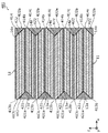
- FIG. 1 is a cross-sectional view showing a cross-sectional structure of a battery according to Embodiment 1.
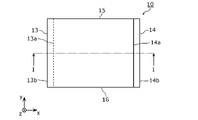
- FIG. 2 is a plan view of a power generating element of the battery according to Embodiment 1.
- FIG. 3A is a cross-sectional view showing a cross-sectional configuration of a first example of a unit cell included in the power generating element according to Embodiment 1.
- FIG. 3B is a cross-sectional view showing a cross-sectional configuration of a second example of a unit cell included in the power generation element according to Embodiment 1.
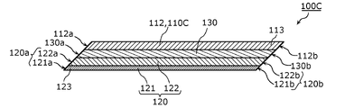
- FIG. 3C is a cross-sectional view showing a cross-sectional configuration of a third example of a unit cell included in the power generation element according to Embodiment 1.
- FIG. 1 is a cross-sectional view showing a cross-sectional structure of a battery according to Embodiment 1.
- FIG. 2 is a plan view of a power generating element of the battery according to Embodiment 1.
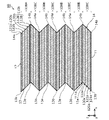
- FIG. 4A is a cross-sectional view showing a cross-sectional configuration of the power generation element according to Embodiment 1.
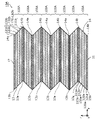
- FIG. 4B is a cross-sectional view showing a cross-sectional configuration of a modification of the power generation element according to Embodiment 1.
- FIG. 5 is a cross-sectional view showing a cross-sectional configuration of a modification of the insulating member according to Embodiment 1.
- FIG. 6 is a cross-sectional view showing a cross-sectional configuration of another modification of the insulating member according to Embodiment 1.
- FIG. 7A is a flowchart showing an example of a method for manufacturing a battery according to Embodiment 1.
- FIG. 7A is a flowchart showing an example of a method for manufacturing a battery according to Embodiment 1.
- FIG. 7B is a flowchart showing another example of the method for manufacturing the battery according to Embodiment 1.
- FIG. FIG. 8 is a cross-sectional view showing a cross-sectional configuration of a battery according to Embodiment 2.
- FIG. 9A is a flowchart showing an example of a method for manufacturing a battery according to Embodiment 2.
- FIG. 9B is a flowchart showing an example of a method for manufacturing a battery according to Embodiment 2.
- FIG. FIG. 10 is a cross-sectional view showing a cross-sectional configuration of a battery according to Embodiment 3.
- FIG. FIG. 11 is a cross-sectional view showing a cross-sectional configuration of a battery according to Embodiment 4.
- FIG. FIG. 12 is a cross-sectional view showing a cross-sectional configuration of a battery according to Embodiment 5.
- FIG. 10 is a cross-sectional view showing a cross-sectional configuration of a battery according to Embod
- a battery according to an aspect of the present disclosure is a battery including a power generation element including a plurality of unit cells having a positive electrode layer, a negative electrode layer, and a solid electrolyte layer positioned between the positive electrode layer and the negative electrode layer, , the plurality of unit cells are electrically connected in parallel and stacked in a direction normal to the main surface, the power generation element has a first side surface and a second side surface, and the first side surface includes the The positive electrode layer of each of the plurality of unit cells protrudes from the negative electrode layer of each of the plurality of unit cells, thereby forming first concave portions and first convex portions alternately arranged along the direction normal to the main surface.
- the negative electrode layer of each of the plurality of unit cells protrudes from the positive electrode layer of each of the plurality of unit cells, thereby alternating along the normal direction of the main surface a second concave portion and a second convex portion are provided in parallel with each other, and the first concave portion includes a first inclined surface that is an end surface of the negative electrode layer and is inclined with respect to the normal direction of the main surface;
- the second recess includes a second inclined surface, which is an end face of the positive electrode layer, inclined with respect to the direction normal to the main surface, and the battery further includes a first insulating member disposed in the first recess.
- the positive electrode layer can protrude from the first side surface of the power generation element, which is a laminate of unit cells.
- the first side surface since the end surface of the negative electrode layer is covered with the first insulating member arranged in the first concave portion, when electrically connecting the first convex portions including the end surfaces of the positive electrode layer, The occurrence of short circuits with layers can be suppressed.
- the negative electrode layer since the end face of the positive electrode layer is an inclined surface, the negative electrode layer can protrude from the second side surface of the power generation element, which is a laminate of unit cells.
- the end face of the positive electrode layer On the second side surface, the end face of the positive electrode layer is covered with the second insulating member disposed in the second recess. The occurrence of short circuits with layers can be suppressed. By suppressing the occurrence of a short circuit, it becomes possible to make the unit cell thinner, so that both high capacity density and high reliability can be achieved.
- the first conductive member may cover the first insulating member
- the second conductive member may cover the second insulating member
- the positive electrode layers can be easily electrically connected by the first conductive member so as to straddle the first insulating member.
- the negative electrode layers can be easily electrically connected by the second conductive member so as to straddle the second insulating member. Therefore, the reliability of the connection between the positive electrode layer and the first conductive member and the reliability of the connection between the negative electrode layer and the second conductive member can be improved.
- the first convex portion includes a third inclined surface that is at least a part of the end surface of the positive electrode layer and is inclined along the normal direction of the main surface, and the second convex portion is the main surface.
- a fourth slanted surface that is at least a part of the end surface of the negative electrode layer and that is slanted along the surface normal direction may be included.
- the end face of the positive electrode layer included in the first protrusion can be separated from the end face of the negative electrode layer included in the first recess.
- the end face of the negative electrode layer included in the second protrusion can be separated from the end face of the positive electrode layer included in the second recess. Therefore, the occurrence of a short circuit between the positive electrode layer and the negative electrode layer can be suppressed more strongly, and the reliability of the battery can be further improved.
- first inclined surface, the third inclined surface, and a part of the end surface of the solid electrolyte layer are flush with each other, and the second inclined surface, the fourth inclined surface, and the A portion of the end face of the solid electrolyte layer may be flush with the part.
- the end face of the positive electrode layer included in the first protrusion can be further separated from the end face of the negative electrode layer included in the first recess.
- the end face of the negative electrode layer included in the second protrusion can be further separated from the end face of the positive electrode layer included in the second recess. Therefore, the occurrence of a short circuit between the positive electrode layer and the negative electrode layer can be suppressed even more strongly.
- the end faces of the positive electrode layer, the solid electrolyte layer and the negative electrode layer can be collectively obliquely processed.
- the first convex portion includes a first flat surface that is at least a part of the end surface of the positive electrode layer parallel to the direction normal to the principal surface, and the second convex portion is parallel to the principal surface direction.
- a second flat surface that is at least a part of the end surface of the negative electrode layer may be included parallel to the line direction.
- the contact between the flat surface, which is at least part of the end surface of the positive electrode layer, and the first conductive member can be improved, so that the connection resistance between the positive electrode layer and the first conductive member can be reduced and the reliability can be improved.
- the contact between the flat surface, which is at least part of the end surface of the negative electrode layer, and the second conductive member can be improved, so that the connection resistance between the negative electrode layer and the second conductive member can be reduced and the reliability can be improved. can be realized.
- first insulating member may have a flush side surface on the first flat surface
- second insulating member may have a flush side surface on the second flat surface
- the positive electrode layers can be covered without gaps by the first conductive member so as to straddle the first insulating member. Good contact with the conductive member can be achieved.
- the negative electrode layers can be covered without gaps by the second conductive member so as to straddle the second insulating member. can make good contact with
- the positive electrode layer of each of the plurality of unit cells includes a positive electrode current collector and a positive electrode active material layer disposed on the main surface of the positive electrode current collector on the negative electrode layer side
- the negative electrode layer of each of the plurality of unit cells may include a negative electrode current collector and a negative electrode active material layer disposed on the main surface of the negative electrode current collector on the positive electrode layer side.
- a plurality of unit cells having the same configuration are stacked while alternately changing the front and back sides, thereby forming a laminate in which the positive electrode layer protrudes from the first side surface and the negative electrode layer protrudes from the second side surface.
- a power generation element can be easily formed.
- two of the positive electrode layers adjacent to each other share the positive electrode current collector
- two of the negative electrode layers adjacent to each other may share the negative electrode current collector
- the number of current collectors can be reduced, and the capacity density of the battery can be further increased.
- At least one of the first conductive member and the second conductive member may have a multilayer structure.
- a conductive material with low connection resistance can be used as the innermost layer in contact with the positive electrode layer or the negative electrode layer, and a highly durable conductive material can be used as the outermost layer. Therefore, the reliability of the battery can be improved.
- the outermost layer of the multilayer structure may be a plating layer or a solder layer.
- the battery according to one aspect of the present disclosure further includes a sealing member that exposes a part of each of the first conductive member and the second conductive member and seals the power generating element.
- the power generation element can be protected from external factors such as moisture and shock, so the reliability of the battery can be improved.
- At least one of the first insulating member and the second insulating member may include a gap.
- the voids can alleviate the stress generated when the power generation element expands or contracts due to the heat generated during battery use. Therefore, damage to the power generation element is suppressed, and the reliability of the battery can be enhanced.
- first side surface and the second side surface may be surfaces that face each other.
- a method for manufacturing a battery according to an aspect of the present disclosure includes a first step of preparing a plurality of unit cells each having a positive electrode layer, a negative electrode layer, and a solid electrolyte layer positioned between the positive electrode layer and the negative electrode layer.
- a first inclined surface inclined with respect to a direction normal to the main surface of each of the plurality of unit cells wherein the first inclined surface inclined with respect to a direction normal to the main surface is provided on an end surface of the negative electrode layer;
- a second inclined surface protruding from the negative electrode layer and inclined with respect to the direction normal to the main surface is provided on the end surface of the positive electrode layer on the second end surface of each of the plurality of unit cells.
- the negative electrode layer protrudes from the positive electrode layer
- the method for manufacturing the battery further includes: facing the positive electrode layers or the negative electrode layers to face each other; a second step of stacking the plurality of unit cells in the direction normal to the main surface with the protruding portions aligned; a third step of disposing a second insulating member so as to cover the surface; disposing a first conductive member for electrically connecting the projecting portions of the positive electrode layer; and a fourth step of placing a second conductive member that connects to the .
- a power generation element having a first side surface from which a positive electrode layer protrudes and a second side surface from which a negative electrode layer protrudes is formed.
- the insulating member By arranging the insulating member in the concave portion of each of the first side surface and the second side surface, the protruding positive electrode layer and the negative electrode layer can be insulated on the first side surface, and the protruding negative electrode layer and the protruding negative electrode layer can be insulated on the second side surface. It can be insulated from the positive electrode layer.
- the third step may be performed after the second step.
- first insulating member and the second insulating member can be collectively arranged in each of the plurality of first recesses and the plurality of second recesses, so that the time required for the process can be shortened.
- the second step may be performed after the third step.
- the first insulating member and the second insulating member can be individually and accurately arranged for each unit cell, so that the occurrence of a short circuit between the positive electrode layer and the negative electrode layer can be suppressed more strongly.
- the first inclined surface and the second inclined surface are provided by processing the first end surface and the second end surface of each of the plurality of unit cells. and the plurality of unit cells may be prepared.
- the processing in the first step may be performed by shear cutting, score cutting, laser cutting, ultrasonic cutting, laser cutting, jet cutting, or polishing.
- the end surfaces of the negative electrode layer, the solid electrolyte layer, and the positive electrode layer are collectively processed by the main surface method. You may incline diagonally with respect to a linear direction.
- the projecting portion of the positive electrode layer and the first insulating member are flattened, and the projecting portion of the negative electrode layer and the second insulating member may be planarized.
- the conductive member can be arranged on a flat surface, so that the connection resistance between each of the positive electrode layer and the negative electrode layer and the conductive member can be reduced and the reliability can be improved.
- each figure is a schematic diagram and is not necessarily strictly illustrated. Therefore, for example, scales and the like do not necessarily match in each drawing. Moreover, in each figure, substantially the same configurations are denoted by the same reference numerals, and overlapping descriptions are omitted or simplified.
- the x-axis, y-axis and z-axis indicate three axes of a three-dimensional orthogonal coordinate system.
- the x-axis and the y-axis are directions parallel to the first side of the rectangle and the second side orthogonal to the first side, respectively, when the power generating element of the battery has a rectangular shape in plan view.
- the z-axis is the stacking direction of a plurality of unit cells included in the power generation element.
- the “stacking direction” corresponds to the direction normal to the main surfaces of the current collector and the active material layer.
- plane view means when viewed from a direction perpendicular to the main surface.
- the terms “upper” and “lower” do not refer to the upward direction (vertically upward) and the downward direction (vertically downward) in absolute spatial recognition, but are based on the stacking order in the stacking structure. It is used as a term defined by a relative positional relationship. Also, the terms “above” and “below” are used only when two components are spaced apart from each other and there is another component between them, as well as when two components are spaced apart from each other. It also applies when two components are in contact with each other and are placed in close contact with each other. In the following description, the negative side of the z-axis is called “lower” or “lower”, and the positive side of the z-axis is called “upper” or “upper”.
- protruding means protruding outward from the center of the unit cell in a cross-sectional view perpendicular to the main surface of the unit cell.
- element A protrudes from element B means that the tip of element A protrudes from the tip of element B in the direction of protrusion, that is, the tip of element A protrudes from the tip of element B by a unit It means away from the center of the cell.
- a “protrusion direction” is regarded as a direction parallel to the main surface of the unit cell.
- the “protruding portion of the element A” means a part of the element A that protrudes from the tip of the element B in the direction of protrusion.
- Elements are, for example, electrode layers, active material layers, solid electrolyte layers, current collectors, and the like.
- ordinal numbers such as “first” and “second” do not mean the number or order of components, unless otherwise specified, to avoid confusion between components of the same kind and to distinguish them. It is used for the purpose of
- FIG. 1 is a cross-sectional view showing the cross-sectional structure of a battery 1 according to this embodiment.
- FIG. 2 is a plan view of power generation element 10 of battery 1 according to the present embodiment.
- FIG. 1 represents a cross section taken along line II shown in FIG.
- the battery 1 includes a power generation element 10 including a plurality of plate-shaped unit cells 100 .
- a plurality of unit cells 100 are electrically connected in parallel and stacked in the direction normal to the main surface.
- the battery 1 is, for example, an all-solid battery.
- Battery 1 further includes insulating members 21 and 22 and conductive members 31 and 32 .
- the power generation element 10 includes eight unit cells 100.
- the number of unit cells 100 included in the power generating element 10 may be plural, for example, two, three or more, or four or more.
- the plan view shape of the power generation element 10 is rectangular as shown in FIG. 2, but is not limited to this.
- the plan view shape of the power generation element 10 may be a polygon such as a square, hexagon or octagon, or may be circular or elliptical.
- the power generation element 10 has main surfaces 11 and 12, as shown in FIG. Principal surfaces 11 and 12 are facing away from each other and parallel to each other.
- the direction orthogonal to the main surface 11 or 12 is the main surface normal direction, which is the z-axis direction in the drawing. Note that in cross-sectional views such as FIG. 1 , the thickness of each layer is exaggerated in order to facilitate understanding of the layer structure of the power generation element 10 .
- the power generation element 10 has side surfaces 13 and 14 facing each other and side surfaces 15 and 16 facing each other.
- the side surface 13 is an example of a first side surface, and as shown in FIG. 1, concave portions 13a and convex portions 13b arranged alternately along the direction normal to the main surface are provided.
- the positive electrode layer 120 of each of the plurality of unit cells 100 protrudes from the negative electrode layer 110 .
- the positive electrode layer 120 protrudes from the negative electrode layer 110 because the end surface of the negative electrode layer 110 is an inclined surface that is inclined with respect to the direction normal to the main surface.
- the concave portion 13a includes an inclined surface that is an end surface of the negative electrode layer 110 .
- An insulating member 21 is arranged in the concave portion 13 a of the side surface 13 .
- a conductive member 31 is provided so as to cover the convex portion 13 b of the side surface 13 .
- the conductive member 31 corresponds to a positive extraction electrode of the power generation element 10 .
- the side surface 14 is an example of a second side surface, and is provided with concave portions 14a and convex portions 14b that are alternately arranged along the direction normal to the main surface.
- the negative electrode layer 110 of each of the plurality of unit cells 100 protrudes from the positive electrode layer 120 .
- the negative electrode layer 110 protrudes from the positive electrode layer 120 because the end surface of the positive electrode layer 120 is an inclined surface that is inclined with respect to the direction normal to the main surface.
- the concave portion 14 a includes an inclined surface that is the end surface of the positive electrode layer 120 .
- An insulating member 22 is arranged in the concave portion 14 a of the side surface 14 .
- a conductive member 32 is provided so as to cover the convex portion 14 b of the side surface 14 .
- the conductive member 32 corresponds to the extraction electrode of the negative electrode of the power generation element 10 .
- the sides 15 and 16 shown in FIG. 2 are planes parallel to each other.
- the side surfaces 15 and 16 are surfaces including long sides of the rectangle in plan view of the power generation element 10 .
- current is extracted from each of side surfaces 13 and 14 of power generation element 10 . Therefore, the distance between the side surfaces 13 and 14 can be increased, and the conductive members 31 and 32 can be separated from each other, thereby suppressing the occurrence of a short circuit.
- each positive electrode layer 120 of each of the plurality of unit cells 100 protrudes from each negative electrode layer 110 . ing. Therefore, each positive electrode layer 120 can be easily electrically connected through the conductive member 31 .
- each negative electrode layer 110 of each of the plurality of unit cells 100 protrudes from each positive electrode layer 120 . . Therefore, each negative electrode layer 110 can be easily electrically connected through the conductive member 32 .
- the unit cell 100 can be made thinner by suppressing the occurrence of a short circuit, it is possible to realize a battery 1 that achieves both high capacity density and high reliability.
- each of the plurality of unit cells 100 has a negative electrode layer 110, a positive electrode layer 120, and a solid electrolyte layer 130 located between the negative electrode layer 110 and the positive electrode layer 120.
- the negative electrode layer 110 includes a negative electrode current collector 111 and a negative electrode active material layer 112 .
- the cathode layer 120 includes a cathode current collector 121 and a cathode active material layer 122 .
- the negative electrode current collector 111, the negative electrode active material layer 112, the solid electrolyte layer 130, the positive electrode active material layer 122, and the positive electrode current collector 121 are laminated in this order in the direction normal to the main surface.
- the configurations of the plurality of unit cells 100 are substantially the same.
- the layers are arranged in the opposite order.
- the negative electrode current collector 111, the negative electrode active material layer 112, the solid electrolyte layer 130, the positive electrode active material layer 122, and the positive electrode current collector 121 stacked in order.
- two adjacent unit cells 100 share either the negative electrode current collector 111 or the positive electrode current collector 121 .
- the unit cell 100 in the bottom layer and the unit cell 100 one above it share the negative electrode current collector 111 .
- two negative electrode layers 110 adjacent to each other share a negative electrode current collector 111 with each other.
- a negative electrode active material layer 112 is provided on both main surfaces of a shared negative electrode current collector 111 .
- the end face of the shared negative electrode current collector 111 is flush with one end face of the two adjacent negative electrode active material layers 112 .
- the two positive electrode layers 120 adjacent to each other share the positive electrode current collector 121 with each other.
- Positive electrode active material layers 122 are provided on both main surfaces of a shared positive electrode current collector 121 .
- the end face of the shared positive electrode current collector 121 is flush with one end face of the two adjacent positive electrode active material layers 122 .
- the negative electrode current collector 111 and the positive electrode current collector 121 are conductive foil-shaped, plate-shaped, or mesh-shaped members, respectively. Each of the negative electrode current collector 111 and the positive electrode current collector 121 may be, for example, a conductive thin film. Examples of materials that constitute the negative electrode current collector 111 and the positive electrode current collector 121 include metals such as stainless steel (SUS), aluminum (Al), copper (Cu), and nickel (Ni). The negative electrode current collector 111 and the positive electrode current collector 121 may be formed using different materials.
- each of the negative electrode current collector 111 and the positive electrode current collector 121 is, for example, 5 ⁇ m or more and 100 ⁇ m or less, but is not limited to this.
- a negative electrode active material layer 112 is in contact with the main surface of the negative electrode current collector 111 .
- the negative electrode current collector 111 may include a current collector layer which is a layer containing a conductive material and provided in a portion in contact with the negative electrode active material layer 112 .
- a cathode active material layer 122 is in contact with the main surface of the cathode current collector 121 .
- the positive electrode current collector 121 may include a current collector layer which is a layer containing a conductive material and provided in a portion in contact with the positive electrode active material layer 122 .
- the negative electrode active material layer 112 is arranged on the main surface of the negative electrode current collector 111 on the positive electrode layer 120 side.
- the negative electrode active material layer 112 contains, for example, a negative electrode active material as an electrode material.
- the negative electrode active material layer 112 is arranged to face the positive electrode active material layer 122 .
- a negative electrode active material such as graphite or metallic lithium can be used.
- Various materials capable of extracting and inserting ions such as lithium (Li) or magnesium (Mg) may be used as materials of the negative electrode active material.
- a solid electrolyte such as an inorganic solid electrolyte may be used.
- an inorganic solid electrolyte for example, a sulfide solid electrolyte or an oxide solid electrolyte can be used.
- a sulfide solid electrolyte for example, a mixture of lithium sulfide (Li 2 S) and phosphorus pentasulfide (P 2 S 5 ) can be used.
- a conductive material such as acetylene black or a binding binder such as polyvinylidene fluoride may be used.
- the negative electrode active material layer 112 is produced by coating the main surface of the negative electrode current collector 111 with a paste-like paint in which the material contained in the negative electrode active material layer 112 is kneaded together with a solvent and drying it.
- the negative electrode layer 110 also referred to as a negative electrode plate
- the thickness of the negative electrode active material layer 112 is, for example, 5 ⁇ m or more and 300 ⁇ m or less, but is not limited thereto.
- the positive electrode active material layer 122 is arranged on the main surface of the positive electrode current collector 121 on the negative electrode layer 110 side.
- the positive electrode active material layer 122 is a layer containing a positive electrode material such as an active material.
- the positive electrode material is the material that constitutes the counter electrode of the negative electrode material.
- the positive electrode active material layer 122 contains, for example, a positive electrode active material.
- Examples of the positive electrode active material contained in the positive electrode active material layer 122 include lithium cobaltate composite oxide (LCO), lithium nickelate composite oxide (LNO), lithium manganate composite oxide (LMO), and lithium-manganese.
- LCO lithium cobaltate composite oxide
- LNO lithium nickelate composite oxide
- LMO lithium manganate composite oxide
- LNMCO lithium-manganese
- LMNO nickel composite oxide
- LMCO lithium-manganese-cobalt composite oxide
- LNCO lithium-nickel-cobalt composite oxide
- LNMCO lithium-nickel-manganese-cobalt composite oxide
- Various materials capable of withdrawing and inserting ions such as Li or Mg can be used as the material of the positive electrode active material.
- a solid electrolyte such as an inorganic solid electrolyte may be used.
- a sulfide solid electrolyte, an oxide solid electrolyte, or the like can be used.
- a sulfide solid electrolyte for example, a mixture of Li2S and P2S5 can be used.
- the surface of the positive electrode active material may be coated with a solid electrolyte.
- a conductive material such as acetylene black, or a binding binder such as polyvinylidene fluoride may be used.
- the positive electrode active material layer 122 is produced by coating the main surface of the positive electrode current collector 121 with a paste-like paint in which the material contained in the positive electrode active material layer 122 is kneaded together with a solvent and drying it.
- the positive electrode layer 120 also referred to as a positive electrode plate
- the thickness of the positive electrode active material layer 122 is, for example, 5 ⁇ m or more and 300 ⁇ m or less, but is not limited thereto.
- the solid electrolyte layer 130 is arranged between the negative electrode active material layer 112 and the positive electrode active material layer 122 . Solid electrolyte layer 130 is in contact with each of negative electrode active material layer 112 and positive electrode active material layer 122 .
- Solid electrolyte layer 130 is a layer containing an electrolyte material. As the electrolyte material, generally known battery electrolytes can be used. The thickness of solid electrolyte layer 130 may be 5 ⁇ m or more and 300 ⁇ m or less, or may be 5 ⁇ m or more and 100 ⁇ m or less.
- Solid electrolyte layer 130 contains a solid electrolyte.
- a solid electrolyte such as an inorganic solid electrolyte can be used.
- an inorganic solid electrolyte a sulfide solid electrolyte, an oxide solid electrolyte, or the like can be used.
- a sulfide solid electrolyte for example, a mixture of Li2S and P2S5 can be used.
- the solid electrolyte layer 130 may contain a binding binder such as polyvinylidene fluoride.
- the negative electrode active material layer 112, the positive electrode active material layer 122, and the solid electrolyte layer 130 are maintained in the form of parallel plates. As a result, it is possible to suppress the occurrence of cracks or collapse due to bending. Note that the negative electrode active material layer 112, the positive electrode active material layer 122, and the solid electrolyte layer 130 may be combined and smoothly curved.
- the negative electrode active material layer 112 may be smaller than the negative electrode current collector 111 in plan view. That is, the main surface of the negative electrode current collector 111 on the positive electrode layer 120 side may have a portion where the negative electrode active material layer 112 is not provided.
- the positive electrode active material layer 122 may be smaller than the positive electrode current collector 121 in plan view. That is, the main surface of the positive electrode current collector 121 on the negative electrode layer 110 side may have a portion where the positive electrode active material layer 122 is not provided.
- a solid electrolyte layer 130 may be provided on a portion of the main surface of each current collector where the active material layer is not provided.
- FIG. 3A is a cross-sectional view showing a cross-sectional configuration of a first example of a unit cell included in power generation element 10 according to the present embodiment.
- a unit cell 100A shown in FIG. 3A is one of the plurality of unit cells 100 shown in FIG. Specifically, the unit cell 100A is the unit cell 100 located in the uppermost layer.
- the unit cell 100A includes a protruding portion 113 in which the negative electrode layer 110 protrudes from the positive electrode layer 120 and a protruding portion 123 in which the positive electrode layer 120 protrudes from the negative electrode layer 110 .
- projecting portion 123 and projecting portion 113 are provided on two end surfaces 103 and 104 of unit cell 100A facing each other.
- the projecting portions 113 and 123 are each formed by cutting the end face of the plate-shaped unit cell 100A obliquely with respect to the direction normal to the main surface.
- the end surfaces of the unit cells 100A are collectively cut, so that the end surfaces become slanted surfaces that are planes slanted with respect to the direction normal to the main surface.
- the end face 103 of the unit cell 100A includes the end face 110a of the negative electrode layer 110, the end face 120a of the positive electrode layer 120, and the end face 130a of the solid electrolyte layer 130. These end faces 110a, 120a and 130a are flush.
- the end face 104 of the unit cell 100A includes the end face 110b of the negative electrode layer 110, the end face 120b of the positive electrode layer 120, and the end face 130b of the solid electrolyte layer 130. These end faces 110b, 120b and 130b are flush.
- the end surfaces 103 and 104 are parallel to each other, for example, but not limited to this. At least one of the end faces 103 and 104 may be a convex or concave curved surface. Also, at least one of the end surfaces 103 and 104 may include a plurality of inclined surfaces with different inclination angles.
- the end surface 110a of the negative electrode layer 110 is an example of a first inclined surface inclined in the direction normal to the main surface.
- the end face 110 a includes the end face 111 a of the negative electrode current collector 111 and the end face 112 a of the negative electrode active material layer 112 .
- the end surfaces 111a and 112a are flush.
- the end surface 120a of the positive electrode layer 120 is an example of a third inclined surface inclined in the direction normal to the main surface.
- End face 120 a includes end face 121 a of positive electrode current collector 121 and end face 122 a of positive electrode active material layer 122 .
- the end faces 121a and 122a are flush.
- the end surface 120a of the positive electrode layer 120 may not be an inclined surface, and may be a surface perpendicular to the main surface. Moreover, at least part of the end surface 130a of the solid electrolyte layer 130 may be a surface perpendicular to the main surface. That is, only the end surface 110a of the negative electrode layer 110, or only the end surface 110a and a part of the end surface 130a of the solid electrolyte layer 130 may be inclined surfaces.
- the end surface 120b of the positive electrode layer 120 is an example of a second inclined surface inclined in the direction normal to the main surface.
- End surface 120 b includes end surface 121 b of positive electrode current collector 121 and end surface 122 b of positive electrode active material layer 122 .
- the end faces 121b and 122b are flush.
- the end surface 110b of the negative electrode layer 110 is an example of a fourth inclined surface inclined in the direction normal to the main surface.
- the end face 110 b includes the end face 111 b of the negative electrode current collector 111 and the end face 112 b of the negative electrode active material layer 112 .
- the end surfaces 111b and 112b are flush.
- the end surface 110b of the negative electrode layer 110 may not be an inclined surface, and may be a surface perpendicular to the main surface. At least part of the end surface 130b of the solid electrolyte layer 130 may be a surface perpendicular to the main surface. That is, only the end surface 120b of the positive electrode layer 120, or only the end surface 120b and part of the end surface 130b of the solid electrolyte layer 130 may be inclined surfaces.
- the power generation element 10 shown in FIG. 1 includes not only the unit cell 100A shown in FIG. 3A, but also the unit cell 100B shown in FIG. 3B and the unit cell 100C shown in FIG. Stacked together.
- 3B and 3C are cross-sectional views showing cross-sectional configurations of second and third examples, respectively, of the unit cell included in the power generation element 10 according to the present embodiment.
- a unit cell 100B shown in FIG. 3B has a configuration in which the positive electrode current collector 121 is removed from the unit cell 100A shown in FIG. 3A. That is, the positive electrode layer 120B of the unit cell 100B includes only the positive electrode active material layer 122. As shown in FIG.
- a unit cell 100C shown in FIG. 3C has a configuration in which the negative electrode current collector 111 is removed from the unit cell 100A shown in FIG. 3A. That is, the negative electrode layer 110C of the unit cell 100C includes only the negative electrode active material layer 112. As shown in FIG. In addition, in FIG. 3C, the stacking order of each layer is reversed from that in FIGS. 3A and 3B.
- FIG. 4A is a cross-sectional view showing the cross-sectional configuration of the power generating element 10 according to this embodiment.
- the unit cells 100B and 100C are alternately stacked on the unit cell 100C, which is the bottom layer, and the unit cell 100A is the top layer on the unit cell 100C. has a laminated structure.
- the number and combination of unit cells included in the power generation element 10 are not particularly limited. For example, only the unit cells 100A may be stacked repeatedly.
- the power generation element 10A shown in FIG. 4B can be formed by stacking a plurality of unit cells 100A so that the layers are alternately arranged. Note that FIG. 4B is a cross-sectional view showing a cross-sectional configuration of a modification of the power generation element of the present embodiment.
- current collectors are not shared between two adjacent unit cells 100A.
- two current collectors of the same polarity are arranged so as to overlap each other.
- an adhesive layer may be provided between the current collectors.
- the adhesive layer is, for example, conductive, but it does not have to be conductive.
- the protrusions 123 of the positive electrode layer 120 are aligned to form the protrusions 13b.
- the protrusions 113 of the negative electrode layer 110 are aligned to form a protrusion 14b.
- the positive electrode layer 120 protrudes to form a protrusion 13b, and the negative electrode layer 110 recesses to form a recess 13a.
- the protruding portions of the positive electrode layers 120 or the protruding portions of the negative electrode layers 110 of two adjacent unit cells 100 are aligned. and recesses 13a are provided.
- five convex portions 13b and four concave portions 13a are alternately and repeatedly arranged one by one along the direction normal to the main surface.
- the recess 13 a is an example of a first recess and includes the end face 110 a of the negative electrode layer 110 .
- recess 13 a includes end face 111 a of negative electrode current collector 111 and end faces 112 a of each of two negative electrode active material layers 112 .
- the concave portion 13a is formed by the end surfaces 111a and 112a being inclined surfaces.
- the inclination angle of the end surface is defined by the angle formed by the main surface 11 and the end surface, and is, for example, 30° or more and 60° or less, and is 45° as an example, but is not limited thereto.
- the smaller the inclination angle the deeper the concave portion 13a can be formed, and the occurrence of a short circuit can be suppressed.
- the larger the tilt angle the larger the effective area of the unit cell 100 can be secured, so a high capacity density can be achieved. The same applies to the recess 14a, which will be described later.
- the convex portion 13 b is an example of a first convex portion and includes the end surface 120 a of the positive electrode layer 120 .
- the convex portion 13 b includes an end face 121 a of the positive electrode current collector 121 and end faces 122 a of the two positive electrode active material layers 122 . Since the end surfaces 121a and 122a are inclined surfaces, the distance between the tip of the projection 13b and the recess 13a can be increased.
- the negative electrode layer 110 protrudes to form a protrusion 14b, and the positive electrode layer 120 recesses to form a recess 14a.
- the protruding portions of the positive electrode layers 120 or the protruding portions of the negative electrode layers 110 of two adjacent unit cells 100 are aligned. and recesses 14a are provided.
- four convex portions 14b and five concave portions 14a are alternately and repeatedly arranged one by one along the direction normal to the main surface.
- the recessed portion 14 a is an example of a second recessed portion and includes the end surface 120 b of the positive electrode layer 120 .
- recess 14 a includes end face 121 b of positive electrode current collector 121 and end faces 122 b of two positive electrode active material layers 122 .
- the concave portion 14a is formed by the end surfaces 121b and 122b being inclined surfaces.
- the convex portion 14b is an example of a second convex portion and includes the end surface 110b of the negative electrode layer 110. As shown in FIG. Specifically, as shown in FIG. 4B, the convex portion 14b includes an end face 111b of the negative electrode current collector 111 and end faces 112b of the two negative electrode active material layers 112 . Since the end surfaces 111b and 112b are inclined surfaces, the distance between the tip of the projection 14b and the recess 14a can be increased.
- end faces 110a, 110b, 120a, 120b, 130a and 130b are as shown in FIG. 4A.
- the insulating member 21 is an example of a first insulating member, and is arranged in the recess 13a as shown in FIG. Specifically, the insulating member 21 covers the end face 110 a of the negative electrode layer 110 . Specifically, the insulating member 21 covers the entire end surface 110 a of the negative electrode layer 110 and also covers the end surface 130 a of the solid electrolyte layer 130 . The insulating member 21 may cover the end face 122 a of the positive electrode active material layer 122 . The insulating member 21 does not cover the end surface 121 a of the positive electrode current collector 121 . By providing insulating member 21 on side surface 13 , at least part of end surface 120 a of positive electrode layer 120 is exposed on side surface 13 without exposing end surface 110 a of negative electrode layer 110 .
- the insulating member 22 is an example of a second insulating member and is arranged in the recess 14a. Specifically, the insulating member 22 covers the end surface 120 b of the positive electrode layer 120 . Specifically, the insulating member 22 covers the entire end surface 120 b of the positive electrode layer 120 and also covers the end surface 130 b of the solid electrolyte layer 130 . The insulating member 22 may cover the end surface 112 b of the negative electrode active material layer 112 . The insulating member 22 does not cover the end surface 111 b of the negative electrode current collector 111 . Since the insulating member 22 is provided on the side surface 14 , at least a portion of the end surface 110 b of the negative electrode layer 110 is exposed on the side surface 14 without exposing the end surface 120 b of the positive electrode layer 120 .
- the insulating members 21 and 22 are each formed using an electrically insulating material.
- an electrically insulating material for example, an epoxy-based resin material can be used, but an inorganic material may also be used.
- Usable insulating materials are selected based on various properties such as flexibility, gas barrier properties, impact resistance, and heat resistance. Insulating members 21 and 22 are made of the same material, but may be made of different materials.
- Insulating members may also be arranged on the side surfaces 15 and 16, respectively.
- the insulating member covers, for example, the entirety of each of the side surfaces 15 and 16 and is connected to the insulating member 21 arranged in the recess 13 a of the side surface 13 and the insulating member 22 arranged in the recess 14 a of the side surface 14 .
- the insulating members 21 and 22 may be formed integrally with the insulating members covering the side surfaces 15 and 16, respectively.
- the outer surface 21a of the insulating member 21 and the outer surface 22a of the insulating member 22 are each flat. Both outer surfaces 21a and 22a are perpendicular to the main surface. Both the outer side surfaces 21a and 22b are located inside the tips of the projections 13b and 14b.
- the shapes of the insulating members 21 and 22 are not limited to the example shown in FIG.
- FIG. 5 is a cross-sectional view showing a modification of the insulating member of this embodiment.
- the insulating members 221 and 222 shown in FIG. 5 have outwardly convexly curved outer surfaces 221a and 222a.
- part of the outer surface 221a may protrude beyond the tip of the projection 13b.
- a part of the outer side surface 222a may protrude beyond the tip of the protrusion 14b.
- At least one of the outer side surfaces 221a and 222a may be concavely curved.
- FIG. 6 is a cross-sectional view showing another modification of the insulating member of this embodiment.
- the insulating members 321 and 322 shown in FIG. 6 have flat outer surfaces 321a and 322a perpendicular to the major surfaces.
- the outer surface 321a is flush with the tip portion of the projection 13b.
- the outer surface 322a is flush with the tip portion of the protrusion 14b.
- each of the projections 13b and 14b is firmly supported by the insulating members 321 and 322, so the occurrence of breakage is suppressed. Therefore, a highly reliable battery can be realized.
- the conductive member 31 is an example of a first conductive member and is in contact with the convex portion 13b. Specifically, the conductive member 31 covers the insulating member 21 . More specifically, the conductive member 31 is provided so as to straddle the insulating member 21 and contact each of the plurality of convex portions 13b. Thereby, the conductive member 31 electrically connects each of the plurality of positive electrode layers 120 and functions as an extraction electrode for the positive electrode of the battery 1 . In the present embodiment, the conductive member 31 covers the entire side surface 13 of the power generation element 10 from the end of the main surface 11 to the end of the main surface 12 .
- the conductive member 32 is an example of a second conductive member and is in contact with the convex portion 14b. Specifically, the conductive member 32 covers the insulating member 22 . More specifically, the conductive member 32 is provided so as to straddle the insulating member 22 and contact each of the plurality of protrusions 14b. Thereby, the conductive member 32 electrically connects each of the plurality of negative electrode layers 110 and functions as an extraction electrode for the negative electrode of the battery 1 . In this embodiment, the conductive member 32 covers the entire side surface 14 of the power generation element 10 from the end of the main surface 11 to the end of the main surface 12 .
- the conductive members 31 and 32 are formed using a conductive resin material or the like. Alternatively, conductive members 31 and 32 may be formed using a metal material such as solder. Conductive materials that can be used are selected based on various properties such as flexibility, gas barrier properties, impact resistance, heat resistance, and solder wettability. Conductive members 31 and 32 are made of the same material, but may be made of different materials.
- each of the conductive members 31 and 32 is not particularly limited.
- the conductive member 31 may cover only part of the side surface 13 .
- the length of the conductive member 31 along the y-axis direction may be shorter than the length of the side surface 13 along the y-axis direction. The same may be applied to the conductive member 32 as well.
- the conductive member 31 may be provided for each convex portion 13b.
- the conductive member 32 may be provided for each convex portion 14b.
- the conductive member 31 and the conductive member 32 are electrically insulated from each other.
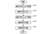
- FIG. 7A is a flow chart showing the manufacturing method of the battery 1 according to this embodiment.
- a plurality of plate-like unit cells are prepared (S10).
- the unit cells to be prepared are, for example, the unit cells before end face processing of each of the unit cells 100A, 100B and 100C shown in FIGS. 3A to 3C.
- the end face before processing is, for example, a plane perpendicular to the main face, but may be an inclined face.
- the end face of each of the plurality of prepared unit cells is obliquely processed (S20).
- the positive electrode layer 120 protrudes from the negative electrode layer 110 by processing the end surface 110a of the negative electrode layer 110 into an inclined surface on the first end surface of each of the plurality of unit cells.
- the end face 120a of the positive electrode layer 120 is processed into an inclined surface, thereby protruding the negative electrode layer 110 from the positive electrode layer 120 .
- the first end surface and the second end surface are respectively the surfaces before processing of the end surfaces 103 and 104 shown in FIG. 3A.
- unit cells 100B and 100C are respectively the surfaces before processing of the end surfaces 103 and 104 shown in FIG. 3A.
- each of the plurality of unit cells are collectively processed. Therefore, all the end surfaces of the negative electrode layer 110, the positive electrode layer 120 and the solid electrolyte layer 130 are inclined surfaces. As a result, unit cells 100A, 100B and 100C having inclined end surfaces are formed.
- the end face is processed by cutting with a cutting blade or by polishing.
- a cutting blade By inclining the cutting blade obliquely with respect to the direction normal to the main surface, an inclined surface is formed on the end surface of the unit cell.
- shear cutting for example, shear cutting, score cutting, razor cutting, ultrasonic cutting, laser cutting, jet cutting, and other various cutting methods can be used.
- various cutting blades such as Goebel slitting blades, gang slitting blades, rotary chopper blades, and shear blades can be used. It is also possible to use a Thomson blade.
- a plurality of unit cells 100A, 100B and 100C are stacked (S30). Specifically, the positive electrode layers 120 or the negative electrode layers 110 face each other, and the projecting portions 123 of the positive electrode layers 120 and the projecting portions 113 of the negative electrode layers 110 are aligned to form a plurality of unit cells 100A, Stack 100B and 100C. Thereby, for example, the power generation element 10 shown in FIG. 4A is formed.
- insulating members 21 and 22 are placed in recesses 13a and 14a, respectively (S40). Specifically, the insulating member 21 is arranged to cover the end surface 110a of the negative electrode layer 110 included in the recess 13a, and the insulating member 22 is arranged to cover the end surface 120b of the positive electrode layer 120 included in the recess 14a.
- the insulating members 21 and 22 are arranged, for example, by applying a fluid resin material and curing it.
- the coating is performed by inkjet or screen printing, or by immersing (dipping) the end face of the unit cell in a resin material.
- Curing is performed by drying, heating, light irradiation, or the like, depending on the resin material used.
- the conductive member 31 that electrically connects the projecting portions 123 of the positive electrode layer 120 is arranged, and the conductive member 32 that electrically connects the projecting portions 113 of the negative electrode layer 110 is arranged (S50).
- the conductive member 31 is arranged by applying a conductive resin so as to cover the outer surface 21a of the insulating member 21 and the convex portion 13b not covered with the insulating member 21 and curing the resin.
- the conductive member 32 is arranged by applying a conductive resin so as to cover the outer surface 22a of the insulating member 22 and the convex portion 14b that is not covered with the insulating member 22 and curing it.
- the conductive members 31 and 32 may be formed by, for example, printing, plating, vapor deposition, sputtering, welding, soldering, joining, or other methods.
- the battery 1 shown in FIG. 1 can be manufactured.
- steps S10 and S20 a single large unit cell may be prepared, and the prepared unit cell may be diagonally cut and individualized to form a plurality of unit cells having inclined end surfaces. good. That is, step S10 and step S20 may be performed in the same process. For example, by singulating a unit cell having both the negative electrode current collector 111 and the positive electrode current collector 121, a plurality of unit cells 100A can be formed. By stacking these unit cells 100A, the power generation element 10A shown in FIG. 4B can be easily formed.
- a step of pressing the plurality of prepared unit cells in the direction normal to the main surface may be performed individually or after stacking the plurality of unit cells.
- FIG. 7A shows an example in which the insulating members 21 and 22 are arranged (S40) after stacking the unit cells (S30), but the present invention is not limited to this.
- the stacking of unit cells (S30) may be performed after the placement of insulating members (S40).
- FIG. 7B is a flow chart showing another example of the method for manufacturing battery 1 according to the present embodiment.
- insulating members are arranged to cover the end surfaces of the unit cells 100A, 100B and 100C before lamination. That is, after the insulating material is individually applied to the end face of each unit cell and cured, a plurality of unit cells are stacked. Note that curing of the insulating material may be performed after lamination.
- step S10 a unit cell having an end face formed with an inclined surface in advance may be prepared. That is, the unit cells 100A, 100B or 100C shown in FIGS. 3A to 3C may be prepared. In this case, the processing (S20) for processing the end faces can be omitted.
- Embodiment 2 differs from Embodiment 1 in that the battery manufacturing method includes a step of flattening the end faces of the projections.
- the following description focuses on the differences from the first embodiment, and omits or simplifies the description of the common points.
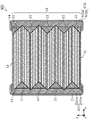
- FIG. 8 is a cross-sectional view showing the cross-sectional structure of battery 401 according to the present embodiment.
- battery 401 includes power generation element 410 and insulating members 421 and 422 .
- battery 401 includes conductive members 31 and 32 in the same manner as in Embodiment 1, the illustration thereof is omitted in FIG.
- a side surface 413 of the power generation element 410 includes concave portions 13a and convex portions 413b that are alternately and repeatedly arranged.
- Each of the plurality of protrusions 413b includes a flat surface 413c.
- the flat surface 413 c is an example of a first flat surface and is at least part of the end surface of the positive electrode layer 120 .
- the flat surface 413 c includes the end face of the positive electrode current collector 121 and part of the end face of the positive electrode active material layer 122 .
- Flat surface 413 c may include a part of the end surface of solid electrolyte layer 130 .
- a side surface 414 of the power generation element 410 includes concave portions 14a and convex portions 414b that are alternately and repeatedly arranged.
- Each of the plurality of protrusions 414b includes a flat surface 414c.
- the flat surface 414 c is an example of a second flat surface and is at least part of the end surface of the negative electrode layer 110 .
- the flat surface 414 c includes the end face of the negative electrode current collector 111 and part of the end face of the negative electrode active material layer 112 .
- Flat surface 414 c may include a part of the end surface of solid electrolyte layer 130 .
- the insulating members 421 are arranged in the plurality of recesses 13a.
- the insulating member 421 has an outer surface 421a.
- the outer surface 421a is flush with the flat surface 413c of the convex portion 413b.
- the insulating members 422 are arranged in the plurality of recesses 14a.
- the insulating member 422 has an outer surface 422a.
- the outer surface 422a is flush with the flat surface 414c of the protrusion 414b.
- the strength of each of the projections 413b and 414b can be increased. Further, since the flat surface 413c and the outer side surface 421a of the insulating member 421 are flush with each other, and the flat surface 414c and the outer side surface 422a of the insulating member 422 are flush with each other, the protrusions 413b and 414b are Each can be strongly supported. Thereby, the risk of collapsing of the positive electrode active material layer 122 and the negative electrode active material layer 112 can be reduced, and the reliability of the battery 401 can be improved.
- FIG. 9A is a flow chart showing an example of a method for manufacturing the battery 401 according to this embodiment.
- the steps (S10 to S40) up to the placement of the insulating member are the same as the steps shown in FIG. 7A of the first embodiment.
- an insulating material may be arranged so as to cover the entire convex portion of the power generation element. A shortage of insulating material can be avoided, and the occurrence of a short circuit can be avoided.
- the side surface of the power generation element 410 is flattened (S45). Specifically, the projecting portion 123 (that is, the projecting portion 413b) of the positive electrode layer 120 and the insulating member 421 are flattened, and the projecting portion 113 (that is, the projecting portion 414b) of the negative electrode layer 110 and the insulating member 422 are flattened. Flatten. For example, the sides are polished until the protrusions are exposed and flat surfaces 413c and 414c are formed. Note that cutting may be performed instead of polishing.
- the conductive members 31 and 32 are arranged so as to cover the flat surface 413c and the outer side surface 421a of the insulating member 421, and the flat surface 414c and the outer side surface 422a of the insulating member 422 (S50). By flattening the surfaces on which the conductive members 31 and 32 are arranged, the conductive members 31 and 32 can be arranged with high accuracy without gaps.
- the present invention is not limited to this.
- the stacking of unit cells (S30) may be performed after the placement of insulating members (S40).
- step S10 a unit cell having an end face formed with an inclined surface in advance may be prepared. That is, the unit cells 100A, 100B or 100C shown in FIGS. 3A to 3C may be prepared. In this case, the processing (S20) for processing the end faces can be omitted.
- the third embodiment differs from the first embodiment in that the battery includes a sealing member.
- the following description focuses on the differences from the first embodiment, and omits or simplifies the description of the common points.
- FIG. 10 is a cross-sectional view showing the cross-sectional structure of battery 501 according to the present embodiment.
- battery 501 further includes a sealing member 540 in addition to the structure of battery 1 according to the first embodiment.
- the sealing member 540 exposes a portion of each of the conductive members 31 and 32 and seals the power generation element 10 .
- the sealing member 540 is provided, for example, so that the power generating element 10 and the insulating members 21 and 22 are not exposed.
- the sealing member 540 is formed using, for example, an electrically insulating insulating material.
- a generally known battery sealing member material such as a sealing agent can be used.
- a resin material can be used as the insulating material.
- the insulating material may be a material that is insulating and does not have ionic conductivity.
- the insulating material may be at least one of epoxy resin, acrylic resin, polyimide resin, and silsesquioxane.
- sealing member 540 may include a plurality of different insulating materials.
- sealing member 540 may have a multilayer structure. Each layer of the multilayer structure may be formed using different materials and have different properties.
- the sealing member 540 may contain a particulate metal oxide material.
- the metal oxide material silicon oxide, aluminum oxide, titanium oxide, zinc oxide, cerium oxide, iron oxide, tungsten oxide, zirconium oxide, calcium oxide, zeolite, glass, etc. can be used.
- the sealing member 540 may be formed using a resin material in which a plurality of particles made of a metal oxide material are dispersed.
- the particle size of the metal oxide material should be equal to or smaller than the space between the positive electrode current collector 121 and the negative electrode current collector 111 .
- the particle shape of the metal oxide material is, for example, spherical, ellipsoidal, or rod-like, but is not limited thereto.
- the sealing member 540 By providing the sealing member 540, the reliability of the battery 501 can be improved in various aspects such as mechanical strength, short-circuit prevention, and moisture resistance.
- the conductive members 31 and 32 are provided so as to be positioned below the current collector in the lowest layer of the power generation element 10, respectively. Specifically, the conductive members 31 and 32 cover part of the outer surface of the sealing member 540 that covers the main surface 11 of the power generation element 10 .
- the mountability can be improved.
- heat radiation performance is improved by forming a gap between the battery 501 and the mounting board.
- At least one of the conductive members 31 and 32 may be provided so as to be positioned above the uppermost current collector of the power generation element 10 . Specifically, at least one of the conductive members 31 and 32 may cover part of the outer surface of the sealing member 540 that covers the main surface 12 of the power generation element 10 .
- the fourth embodiment differs from the first embodiment in that the conductive member has a multilayer structure.
- the following description focuses on the differences from the first embodiment, and omits or simplifies the description of the common points.
- FIG. 11 is a cross-sectional view showing the cross-sectional structure of the battery 601 according to this embodiment.
- battery 601 includes conductive members 631 and 632 instead of conductive members 31 and 32, unlike battery 1 according to the first embodiment.
- the conductive member 631 has a multilayer structure. Specifically, the conductive member 631 includes a first layer 631a and a second layer 631b.
- the first layer 631 a is the innermost layer of the multilayer structure and is a layer that covers the protruding portion 123 of the positive electrode layer 120 exposed on the side surface 13 .
- the first layer 631 a is formed using, for example, a conductive material that has good contact with the positive electrode layer 120 .
- the second layer 631b is the outermost layer of the multilayer structure and is the layer exposed to the outside of the battery 601.
- the second layer 631b is, for example, a plated layer or a solder layer.
- the second layer 631b is formed by methods such as plating, printing, and soldering, for example.
- the conductive member 632 has a multilayer structure. Specifically, the conductive member 631 includes a first layer 632a and a second layer 632b.
- the first layer 632a is the innermost layer of the multilayer structure, and is a layer that covers the protruding portion 113 of the negative electrode layer 110 exposed on the side surface 14.
- the first layer 632 a is formed using, for example, a conductive material that has good contact with the negative electrode layer 110 .
- the second layer 632b is the outermost layer of the multilayer structure and is the layer exposed to the outside of the battery 601.
- the second layer 632b is, for example, a plated layer or a solder layer.
- the second layer 632b is formed by methods such as plating, printing, and soldering, for example.
- the mountability of the battery 601 can be improved by forming the second layers 631b and 632b using a material suitable for mounting on the substrate.
- the first layer 631a or 632a may have higher gas barrier properties than the second layer 631b or 632b.
- the second layer 631b or 632b may be more flexible, impact resistant, or solder wettable than the first layer 631a or 632a.
- the second layer 631b does not have to cover the entire outer surface of the first layer 631a.
- the second layer 631b may cover only a portion of the first layer 631a.
- the second layer 631b may be formed only on the mounting portion on the substrate.
- the number of layers included in the conductive members 631 and 632 may be three or more.
- One of the conductive members 631 and 632 may have a single layer structure as in the first embodiment.
- Embodiment 5 Next, Embodiment 5 will be described.
- the fifth embodiment differs from the first embodiment in that the insulating member includes voids.
- the following description focuses on the differences from the first embodiment, and omits or simplifies the description of the common points.
- FIG. 12 is a cross-sectional view showing the cross-sectional structure of battery 701 according to the present embodiment.
- battery 701 includes insulating members 721 and 722 instead of insulating members 21 and 22, as compared with battery 1 according to the first embodiment.
- Each of the insulating members 721 and 722 includes an air gap 723 .
- the void 723 is a space filled with a predetermined gas.
- the gas is, for example, dry air, but is not limited thereto.
- the size and shape of the gap 723 are also not particularly limited.
- the gap 723 may be provided between the insulating member 721 and the side surface 13 of the power generating element 10 or between the insulating member 722 and the side surface 14 of the power generating element 10 .
- the gap 723 may be provided between the insulating member 721 and the conductive member 31 or between the insulating member 722 and the conductive member 32 .
- the unit cell 100 need not be limited to one minimum unit consisting of the negative electrode layer 110, the positive electrode layer 120 and the solid electrolyte layer 130.
- a unit cell 100 may include a number of smallest units stacked in the direction normal to the main surface.
- the first side surface where the positive electrode layer 120 protrudes from the negative electrode layer 110 is the side surface 13 shown in FIG.
- the first side may be side 15 or 16 . That is, the first side surface where the positive electrode layer protrudes from the negative electrode layer and the second side surface where the negative electrode layer protrudes from the positive electrode layer may be connected to each other.
- the first and second sides may be sides 15 and 16, respectively. In other words, the electrodes may be taken out from the long sides of the power generation element 10 having a rectangular shape in plan view.
- first side and the second side may be one side of the power generation element 10 .
- first side may be part of any one of sides 13-16 and the second side may be another part of the same side.
- the present disclosure can be used, for example, as batteries for electronic equipment, electric appliance devices, electric vehicles, and the like.
Landscapes
- Chemical & Material Sciences (AREA)
- Chemical Kinetics & Catalysis (AREA)
- Electrochemistry (AREA)
- General Chemical & Material Sciences (AREA)
- Engineering & Computer Science (AREA)
- Manufacturing & Machinery (AREA)
- Secondary Cells (AREA)
- Connection Of Batteries Or Terminals (AREA)
Abstract
Description
本開示の一態様に係る電池は、正極層、負極層、および、前記正極層と前記負極層との間に位置する固体電解質層を有する複数の単位セルを含む発電要素を備える電池であって、前記複数の単位セルは、電気的に並列に接続され、かつ、主面法線方向に積層され、前記発電要素は、第1側面および第2側面を有し、前記第1側面では、前記複数の単位セルの各々の前記正極層が前記複数の単位セルの各々の前記負極層より突出することで、前記主面法線方向に沿って交互に並んだ第1凹部および第1凸部が設けられており、前記第2側面では、前記複数の単位セルの各々の前記負極層が前記複数の単位セルの各々の前記正極層より突出することで、前記主面法線方向に沿って交互に並んだ第2凹部および第2凸部が設けられており、前記第1凹部は、前記主面法線方向に対して傾斜した、前記負極層の端面である第1傾斜面を含み、前記第2凹部は、前記主面法線方向に対して傾斜した、前記正極層の端面である第2傾斜面を含み、前記電池は、さらに、前記第1凹部に配置された第1絶縁部材と、前記第2凹部に配置された第2絶縁部材と、前記第1凸部に接触する第1導電部材と、前記第2凸部に接触する第2導電部材と、を備え、前記複数の単位セルの各々の前記正極層は、前記第1導電部材を介して、電気的に接続され、前記複数の単位セルの各々の前記負極層は、前記第2導電部材を介して、電気的に接続されている。
[1.概要]
まず、実施の形態1に係る電池の概要について、図1および図2を用いて説明する。
次に、単位セル100の構成について図1を用いて説明する。
続いて、単位セル100の端面構造について、図3Aを用いて説明する。図3Aは、本実施の形態に係る発電要素10に含まれる単位セルの第1例の断面構成を示す断面図である。
続いて、発電要素10の側面構造について、図1を適宜参照しながら図3A、図3B、図3C、図4Aおよび図4Bを用いて説明する。
次に、絶縁部材21および22について、図1を用いて説明する。なお、以下の説明において、端面110a、110b、120a、120b、130aおよび130bは、図4Aに示した通りである。
次に、導電部材31および32について、図1を用いて説明する。
続いて、電池1の製造方法について、図7Aを用いて説明する。
続いて、実施の形態2について説明する。
続いて、実施の形態3について説明する。
続いて、実施の形態4について説明する。
続いて、実施の形態5について説明する。
以上、1つまたは複数の態様に係る電池および電池の製造方法について、実施の形態に基づいて説明したが、本開示は、これらの実施の形態に限定されるものではない。本開示の主旨を逸脱しない限り、当業者が思いつく各種変形を本実施の形態に施したもの、および、異なる実施の形態における構成要素を組み合わせて構築される形態も、本開示の範囲内に含まれる。
10、10A、410 発電要素
11、12 主面
13、14、15、16、413、414 側面
13a、14a 凹部
13b、14b、413b、414b 凸部
21、22、221、222、321、322、421、422、721、722 絶縁部材
21a、22a、221a、222a、321a、322a、421a、422a 外側面
31、32、631、632 導電部材
100、100A、100B、100C 単位セル
103、104、110a、110b、111a、111b、112a、112b、120a、120b、121a、121b、122a、122b、130a、130b 端面
110、110C 負極層
111 負極集電体
112 負極活物質層
113、123 突出部
120、120B 正極層
121 正極集電体
122 正極活物質層
130 固体電解質層
413c、414c 平坦面
540 封止部材
631a、632a 第1層
631b、632b 第2層
723 空隙
Claims (20)
- 正極層、負極層、および、前記正極層と前記負極層との間に位置する固体電解質層を有する複数の単位セルを含む発電要素を備える電池であって、
前記複数の単位セルは、電気的に並列に接続され、かつ、主面法線方向に積層され、
前記発電要素は、第1側面および第2側面を有し、
前記第1側面では、前記複数の単位セルの各々の前記正極層が前記複数の単位セルの各々の前記負極層より突出することで、前記主面法線方向に沿って交互に並んだ第1凹部および第1凸部が設けられており、
前記第2側面では、前記複数の単位セルの各々の前記負極層が前記複数の単位セルの各々の前記正極層より突出することで、前記主面法線方向に沿って交互に並んだ第2凹部および第2凸部が設けられており、
前記第1凹部は、前記主面法線方向に対して傾斜した、前記負極層の端面である第1傾斜面を含み、
前記第2凹部は、前記主面法線方向に対して傾斜した、前記正極層の端面である第2傾斜面を含み、
前記電池は、さらに、
前記第1凹部に配置された第1絶縁部材と、
前記第2凹部に配置された第2絶縁部材と、
前記第1凸部に接触する第1導電部材と、
前記第2凸部に接触する第2導電部材と、を備え、
前記複数の単位セルの各々の前記正極層は、前記第1導電部材を介して、電気的に接続され、
前記複数の単位セルの各々の前記負極層は、前記第2導電部材を介して、電気的に接続されている、
電池。 - 前記第1導電部材は、前記第1絶縁部材を覆っており、
前記第2導電部材は、前記第2絶縁部材を覆っている、
請求項1に記載の電池。 - 前記第1凸部は、前記主面法線方向に沿って傾斜した、前記正極層の端面の少なくとも一部である第3傾斜面を含み、
前記第2凸部は、前記主面法線方向に沿って傾斜した、前記負極層の端面の少なくとも一部である第4傾斜面を含む、
請求項1または2に記載の電池。 - 前記第1傾斜面と、前記第3傾斜面と、前記固体電解質層の端面の一部とは、面一であり、
前記第2傾斜面と、前記第4傾斜面と、前記固体電解質層の端面の一部とは、面一である、
請求項3に記載の電池。 - 前記第1凸部は、前記主面法線方向に平行な、前記正極層の端面の少なくとも一部である第1平坦面を含み、
前記第2凸部は、前記主面法線方向に平行な、前記負極層の端面の少なくとも一部である第2平坦面を含む、
請求項1から4のいずれか1項に記載の電池。 - 前記第1絶縁部材は、前記第1平坦面に面一な側面を有し、
前記第2絶縁部材は、前記第2平坦面に面一な側面を有する、
請求項5に記載の電池。 - 前記複数の単位セルの各々の前記正極層は、
正極集電体と、
前記正極集電体の、前記負極層側の主面に配置された正極活物質層と、を含み、
前記複数の単位セルの各々の前記負極層は、
負極集電体と、
前記負極集電体の、前記正極層側の主面に配置された負極活物質層と、を含む、
請求項1から6のいずれか1項に記載の電池。 - 前記複数の単位セルにおいて、互いに隣接する2つの前記正極層は、互いの前記正極集電体を共有し、
前記複数の単位セルにおいて、互いに隣接する2つの前記負極層は、互いの前記負極集電体を共有している、
請求項7に記載の電池。 - 前記第1導電部材および前記第2導電部材の少なくとも一方は、多層構造を有する、
請求項1から8のいずれか1項に記載の電池。 - 前記多層構造の最外層は、めっき層または半田層である、
請求項9に記載の電池。 - さらに、前記第1導電部材および前記第2導電部材の各々の一部を露出させ、かつ、前記発電要素を封止する封止部材を備える、
請求項1から10のいずれか1項に記載の電池。 - 前記第1絶縁部材および前記第2絶縁部材の少なくとも一方は、空隙を含む、
請求項1から11のいずれか1項に記載の電池。 - 前記第1側面および前記第2側面は、互いに背向する面である、
請求項1から12のいずれか1項に記載の電池。 - 電池の製造方法であって、
正極層、負極層、および、前記正極層と前記負極層との間に位置する固体電解質層を有する複数の単位セルを準備する第1ステップを含み、
前記複数の単位セルの各々の第1端面では、主面法線方向に対して傾斜した第1傾斜面が前記負極層の端面に設けられていることにより、前記正極層が前記負極層より突出しており、
前記複数の単位セルの各々の第2端面では、前記主面法線方向に対して傾斜した第2傾斜面が前記正極層の端面に設けられていることにより、前記負極層が前記正極層より突出しており、
前記電池の製造方法は、さらに、
前記正極層同士または前記負極層同士を向かい合わせて、かつ、前記正極層の突出部同士、および、前記負極層の突出部同士を揃えて、前記複数の単位セルを前記主面法線方向に積層する第2ステップと、
前記第1傾斜面を覆うように第1絶縁部材を配置し、かつ、前記第2傾斜面を覆うように第2絶縁部材を配置する第3ステップと、
前記正極層の突出部同士を電気的に接続する第1導電部材を配置し、かつ、前記負極層の突出部同士を電気的に接続する第2導電部材を配置する第4ステップと、を含む、
電池の製造方法。 - 前記第3ステップは、前記第2ステップの後に行われる、
請求項14に記載の電池の製造方法。 - 前記第2ステップは、前記第3ステップの後に行われる、
請求項14に記載の電池の製造方法。 - 前記第1ステップでは、前記複数の単位セルの各々の前記第1端面および前記第2端面の各々の加工を行うことにより、前記第1傾斜面および前記第2傾斜面が設けられた前記複数の単位セルを準備する、
請求項14から16のいずれか1項に記載の電池の製造方法。 - 前記第1ステップにおける前記加工は、シアー切断、スコアー切断、レザー切断、超音波切断、レーザー切断、ジェット切断、または、研磨によって行われる、
請求項17に記載の電池の製造方法。 - 前記第1ステップにおける前記加工では、前記第1端面および前記第2端面の各々において、前記負極層、前記固体電解質層および前記正極層の各々の端面を一括して前記主面法線方向に対して斜めに傾斜させる、
請求項17または18に記載の電池の製造方法。 - さらに、前記第2ステップおよび前記第3ステップが行われた後、前記第4ステップを行う前に、前記正極層の突出部と前記第1絶縁部材とを平坦化し、かつ、前記負極層の突出部と前記第2絶縁部材とを平坦化する、
請求項14から19のいずれか1項に記載の電池の製造方法。
Priority Applications (4)
| Application Number | Priority Date | Filing Date | Title |
|---|---|---|---|
| JP2022581228A JP7748657B2 (ja) | 2021-02-15 | 2021-12-23 | 電池および電池の製造方法 |
| EP21925861.3A EP4293774A4 (en) | 2021-02-15 | 2021-12-23 | BATTERY AND METHOD FOR MANUFACTURING THE BATTERY |
| CN202180092993.8A CN116830330A (zh) | 2021-02-15 | 2021-12-23 | 电池及电池的制造方法 |
| US18/362,570 US20240021959A1 (en) | 2021-02-15 | 2023-07-31 | Battery and method for manufacturing battery |
Applications Claiming Priority (2)
| Application Number | Priority Date | Filing Date | Title |
|---|---|---|---|
| JP2021022052 | 2021-02-15 | ||
| JP2021-022052 | 2021-02-15 |
Related Child Applications (1)
| Application Number | Title | Priority Date | Filing Date |
|---|---|---|---|
| US18/362,570 Continuation US20240021959A1 (en) | 2021-02-15 | 2023-07-31 | Battery and method for manufacturing battery |
Publications (1)
| Publication Number | Publication Date |
|---|---|
| WO2022172618A1 true WO2022172618A1 (ja) | 2022-08-18 |
Family
ID=82838679
Family Applications (1)
| Application Number | Title | Priority Date | Filing Date |
|---|---|---|---|
| PCT/JP2021/047812 Ceased WO2022172618A1 (ja) | 2021-02-15 | 2021-12-23 | 電池および電池の製造方法 |
Country Status (5)
| Country | Link |
|---|---|
| US (1) | US20240021959A1 (ja) |
| EP (1) | EP4293774A4 (ja) |
| JP (1) | JP7748657B2 (ja) |
| CN (1) | CN116830330A (ja) |
| WO (1) | WO2022172618A1 (ja) |
Cited By (2)
| Publication number | Priority date | Publication date | Assignee | Title |
|---|---|---|---|---|
| KR20240092675A (ko) | 2022-12-14 | 2024-06-24 | 삼성에스디아이 주식회사 | 전고체 이차전지 |
| WO2025225070A1 (ja) * | 2024-04-26 | 2025-10-30 | パナソニックIpマネジメント株式会社 | 電池、電池の製造方法及び電池の製造装置 |
Citations (6)
| Publication number | Priority date | Publication date | Assignee | Title |
|---|---|---|---|---|
| JP2009016188A (ja) | 2007-07-05 | 2009-01-22 | Toyota Motor Corp | 電池 |
| JP2013518394A (ja) * | 2010-01-26 | 2013-05-20 | シンベット・コーポレイション | 電池アレイ、構造及び方法 |
| JP2015233003A (ja) | 2014-05-16 | 2015-12-24 | 株式会社半導体エネルギー研究所 | 二次電池を備えた電子機器 |
| WO2017014233A1 (ja) * | 2015-07-22 | 2017-01-26 | 株式会社豊田自動織機 | リチウムイオン二次電池の電極組立体及びその製造方法 |
| WO2019039412A1 (ja) | 2017-08-23 | 2019-02-28 | 株式会社村田製作所 | 積層構造体及びその製造方法、並びに、ロールプレス装置 |
| WO2020183795A1 (ja) * | 2019-03-12 | 2020-09-17 | パナソニックIpマネジメント株式会社 | 積層電池 |
Family Cites Families (1)
| Publication number | Priority date | Publication date | Assignee | Title |
|---|---|---|---|---|
| WO2022080404A1 (ja) * | 2020-10-16 | 2022-04-21 | 株式会社村田製作所 | 固体電池 |
-
2021
- 2021-12-23 CN CN202180092993.8A patent/CN116830330A/zh active Pending
- 2021-12-23 JP JP2022581228A patent/JP7748657B2/ja active Active
- 2021-12-23 EP EP21925861.3A patent/EP4293774A4/en not_active Withdrawn
- 2021-12-23 WO PCT/JP2021/047812 patent/WO2022172618A1/ja not_active Ceased
-
2023
- 2023-07-31 US US18/362,570 patent/US20240021959A1/en active Pending
Patent Citations (6)
| Publication number | Priority date | Publication date | Assignee | Title |
|---|---|---|---|---|
| JP2009016188A (ja) | 2007-07-05 | 2009-01-22 | Toyota Motor Corp | 電池 |
| JP2013518394A (ja) * | 2010-01-26 | 2013-05-20 | シンベット・コーポレイション | 電池アレイ、構造及び方法 |
| JP2015233003A (ja) | 2014-05-16 | 2015-12-24 | 株式会社半導体エネルギー研究所 | 二次電池を備えた電子機器 |
| WO2017014233A1 (ja) * | 2015-07-22 | 2017-01-26 | 株式会社豊田自動織機 | リチウムイオン二次電池の電極組立体及びその製造方法 |
| WO2019039412A1 (ja) | 2017-08-23 | 2019-02-28 | 株式会社村田製作所 | 積層構造体及びその製造方法、並びに、ロールプレス装置 |
| WO2020183795A1 (ja) * | 2019-03-12 | 2020-09-17 | パナソニックIpマネジメント株式会社 | 積層電池 |
Non-Patent Citations (1)
| Title |
|---|
| See also references of EP4293774A4 |
Cited By (3)
| Publication number | Priority date | Publication date | Assignee | Title |
|---|---|---|---|---|
| KR20240092675A (ko) | 2022-12-14 | 2024-06-24 | 삼성에스디아이 주식회사 | 전고체 이차전지 |
| KR102869525B1 (ko) * | 2022-12-14 | 2025-10-14 | 삼성에스디아이 주식회사 | 전고체 이차전지 |
| WO2025225070A1 (ja) * | 2024-04-26 | 2025-10-30 | パナソニックIpマネジメント株式会社 | 電池、電池の製造方法及び電池の製造装置 |
Also Published As
| Publication number | Publication date |
|---|---|
| US20240021959A1 (en) | 2024-01-18 |
| EP4293774A1 (en) | 2023-12-20 |
| JPWO2022172618A1 (ja) | 2022-08-18 |
| CN116830330A (zh) | 2023-09-29 |
| JP7748657B2 (ja) | 2025-10-03 |
| EP4293774A4 (en) | 2024-11-06 |
Similar Documents
| Publication | Publication Date | Title |
|---|---|---|
| WO2022172619A1 (ja) | 電池および電池の製造方法 | |
| JP7378097B2 (ja) | 積層電池 | |
| US12074292B2 (en) | Laminated battery | |
| JP2022124376A (ja) | 電池および電池の製造方法 | |
| US20240258666A1 (en) | Battery and method for manufacturing battery | |
| US20240021959A1 (en) | Battery and method for manufacturing battery | |
| JP7804890B2 (ja) | 電池 | |
| WO2023053638A1 (ja) | 電池および電池の製造方法 | |
| US20240072392A1 (en) | Battery and method of manufacturing battery | |
| US20240072381A1 (en) | Battery and method of manufacturing battery | |
| JP7818203B2 (ja) | 電池および電池の製造方法 | |
| EP4340091A1 (en) | Battery and method for manufacturing battery | |
| WO2023145223A1 (ja) | 電池および電池の製造方法 | |
| JP7565525B2 (ja) | 電池の製造方法 | |
| WO2023058294A1 (ja) | 電池および電池の製造方法 | |
| JP7837007B2 (ja) | 電池および電池の製造方法 | |
| WO2024062778A1 (ja) | 電池およびその製造方法 | |
| WO2023053639A1 (ja) | 電池および電池の製造方法 | |
| WO2023053637A1 (ja) | 電池および電池の製造方法 | |
| WO2023203795A1 (ja) | 電池およびその製造方法 | |
| WO2023053640A1 (ja) | 電池および電池の製造方法 |
Legal Events
| Date | Code | Title | Description |
|---|---|---|---|
| 121 | Ep: the epo has been informed by wipo that ep was designated in this application |
Ref document number: 21925861 Country of ref document: EP Kind code of ref document: A1 |
|
| ENP | Entry into the national phase |
Ref document number: 2022581228 Country of ref document: JP Kind code of ref document: A |
|
| WWE | Wipo information: entry into national phase |
Ref document number: 202180092993.8 Country of ref document: CN |
|
| WWE | Wipo information: entry into national phase |
Ref document number: 2021925861 Country of ref document: EP |
|
| NENP | Non-entry into the national phase |
Ref country code: DE |
|
| ENP | Entry into the national phase |
Ref document number: 2021925861 Country of ref document: EP Effective date: 20230915 |
|
| WWW | Wipo information: withdrawn in national office |
Ref document number: 2021925861 Country of ref document: EP |