WO2022172862A1 - 半導体基板洗浄用組成物、並びに半導体基板の洗浄方法および製造方法 - Google Patents
半導体基板洗浄用組成物、並びに半導体基板の洗浄方法および製造方法 Download PDFInfo
- Publication number
- WO2022172862A1 WO2022172862A1 PCT/JP2022/004347 JP2022004347W WO2022172862A1 WO 2022172862 A1 WO2022172862 A1 WO 2022172862A1 JP 2022004347 W JP2022004347 W JP 2022004347W WO 2022172862 A1 WO2022172862 A1 WO 2022172862A1
- Authority
- WO
- WIPO (PCT)
- Prior art keywords
- group
- semiconductor substrate
- composition
- acid
- cleaning
- Prior art date
- Legal status (The legal status is an assumption and is not a legal conclusion. Google has not performed a legal analysis and makes no representation as to the accuracy of the status listed.)
- Ceased
Links
Images

Classifications
-
- H—ELECTRICITY
- H10—SEMICONDUCTOR DEVICES; ELECTRIC SOLID-STATE DEVICES NOT OTHERWISE PROVIDED FOR
- H10P—GENERIC PROCESSES OR APPARATUS FOR THE MANUFACTURE OR TREATMENT OF DEVICES COVERED BY CLASS H10
- H10P50/00—Etching of wafers, substrates or parts of devices
- H10P50/20—Dry etching; Plasma etching; Reactive-ion etching
- H10P50/28—Dry etching; Plasma etching; Reactive-ion etching of insulating materials
- H10P50/282—Dry etching; Plasma etching; Reactive-ion etching of insulating materials of inorganic materials
- H10P50/283—Dry etching; Plasma etching; Reactive-ion etching of insulating materials of inorganic materials by chemical means
-
- C—CHEMISTRY; METALLURGY
- C11—ANIMAL OR VEGETABLE OILS, FATS, FATTY SUBSTANCES OR WAXES; FATTY ACIDS THEREFROM; DETERGENTS; CANDLES
- C11D—DETERGENT COMPOSITIONS; USE OF SINGLE SUBSTANCES AS DETERGENTS; SOAP OR SOAP-MAKING; RESIN SOAPS; RECOVERY OF GLYCEROL
- C11D3/00—Other compounding ingredients of detergent compositions covered in group C11D1/00
- C11D3/16—Organic compounds
- C11D3/24—Organic compounds containing halogen
- C11D3/245—Organic compounds containing halogen containing fluorine
-
- C—CHEMISTRY; METALLURGY
- C11—ANIMAL OR VEGETABLE OILS, FATS, FATTY SUBSTANCES OR WAXES; FATTY ACIDS THEREFROM; DETERGENTS; CANDLES
- C11D—DETERGENT COMPOSITIONS; USE OF SINGLE SUBSTANCES AS DETERGENTS; SOAP OR SOAP-MAKING; RESIN SOAPS; RECOVERY OF GLYCEROL
- C11D3/00—Other compounding ingredients of detergent compositions covered in group C11D1/00
- C11D3/39—Organic or inorganic per-compounds
-
- C—CHEMISTRY; METALLURGY
- C11—ANIMAL OR VEGETABLE OILS, FATS, FATTY SUBSTANCES OR WAXES; FATTY ACIDS THEREFROM; DETERGENTS; CANDLES
- C11D—DETERGENT COMPOSITIONS; USE OF SINGLE SUBSTANCES AS DETERGENTS; SOAP OR SOAP-MAKING; RESIN SOAPS; RECOVERY OF GLYCEROL
- C11D3/00—Other compounding ingredients of detergent compositions covered in group C11D1/00
- C11D3/0005—Other compounding ingredients characterised by their effect
- C11D3/0073—Anticorrosion compositions
-
- C—CHEMISTRY; METALLURGY
- C11—ANIMAL OR VEGETABLE OILS, FATS, FATTY SUBSTANCES OR WAXES; FATTY ACIDS THEREFROM; DETERGENTS; CANDLES
- C11D—DETERGENT COMPOSITIONS; USE OF SINGLE SUBSTANCES AS DETERGENTS; SOAP OR SOAP-MAKING; RESIN SOAPS; RECOVERY OF GLYCEROL
- C11D3/00—Other compounding ingredients of detergent compositions covered in group C11D1/00
- C11D3/16—Organic compounds
- C11D3/24—Organic compounds containing halogen
-
- C—CHEMISTRY; METALLURGY
- C11—ANIMAL OR VEGETABLE OILS, FATS, FATTY SUBSTANCES OR WAXES; FATTY ACIDS THEREFROM; DETERGENTS; CANDLES
- C11D—DETERGENT COMPOSITIONS; USE OF SINGLE SUBSTANCES AS DETERGENTS; SOAP OR SOAP-MAKING; RESIN SOAPS; RECOVERY OF GLYCEROL
- C11D7/00—Compositions of detergents based essentially on non-surface-active compounds
- C11D7/02—Inorganic compounds
- C11D7/04—Water-soluble compounds
- C11D7/08—Acids
-
- C—CHEMISTRY; METALLURGY
- C11—ANIMAL OR VEGETABLE OILS, FATS, FATTY SUBSTANCES OR WAXES; FATTY ACIDS THEREFROM; DETERGENTS; CANDLES
- C11D—DETERGENT COMPOSITIONS; USE OF SINGLE SUBSTANCES AS DETERGENTS; SOAP OR SOAP-MAKING; RESIN SOAPS; RECOVERY OF GLYCEROL
- C11D7/00—Compositions of detergents based essentially on non-surface-active compounds
- C11D7/02—Inorganic compounds
- C11D7/04—Water-soluble compounds
- C11D7/10—Salts
-
- C—CHEMISTRY; METALLURGY
- C11—ANIMAL OR VEGETABLE OILS, FATS, FATTY SUBSTANCES OR WAXES; FATTY ACIDS THEREFROM; DETERGENTS; CANDLES
- C11D—DETERGENT COMPOSITIONS; USE OF SINGLE SUBSTANCES AS DETERGENTS; SOAP OR SOAP-MAKING; RESIN SOAPS; RECOVERY OF GLYCEROL
- C11D7/00—Compositions of detergents based essentially on non-surface-active compounds
- C11D7/22—Organic compounds
- C11D7/26—Organic compounds containing oxygen
-
- C—CHEMISTRY; METALLURGY
- C11—ANIMAL OR VEGETABLE OILS, FATS, FATTY SUBSTANCES OR WAXES; FATTY ACIDS THEREFROM; DETERGENTS; CANDLES
- C11D—DETERGENT COMPOSITIONS; USE OF SINGLE SUBSTANCES AS DETERGENTS; SOAP OR SOAP-MAKING; RESIN SOAPS; RECOVERY OF GLYCEROL
- C11D7/00—Compositions of detergents based essentially on non-surface-active compounds
- C11D7/22—Organic compounds
- C11D7/32—Organic compounds containing nitrogen
- C11D7/3209—Amines or imines with one to four nitrogen atoms; Quaternized amines
-
- C—CHEMISTRY; METALLURGY
- C11—ANIMAL OR VEGETABLE OILS, FATS, FATTY SUBSTANCES OR WAXES; FATTY ACIDS THEREFROM; DETERGENTS; CANDLES
- C11D—DETERGENT COMPOSITIONS; USE OF SINGLE SUBSTANCES AS DETERGENTS; SOAP OR SOAP-MAKING; RESIN SOAPS; RECOVERY OF GLYCEROL
- C11D7/00—Compositions of detergents based essentially on non-surface-active compounds
- C11D7/22—Organic compounds
- C11D7/34—Organic compounds containing sulfur
-
- C—CHEMISTRY; METALLURGY
- C11—ANIMAL OR VEGETABLE OILS, FATS, FATTY SUBSTANCES OR WAXES; FATTY ACIDS THEREFROM; DETERGENTS; CANDLES
- C11D—DETERGENT COMPOSITIONS; USE OF SINGLE SUBSTANCES AS DETERGENTS; SOAP OR SOAP-MAKING; RESIN SOAPS; RECOVERY OF GLYCEROL
- C11D7/00—Compositions of detergents based essentially on non-surface-active compounds
- C11D7/22—Organic compounds
- C11D7/36—Organic compounds containing phosphorus
-
- H—ELECTRICITY
- H10—SEMICONDUCTOR DEVICES; ELECTRIC SOLID-STATE DEVICES NOT OTHERWISE PROVIDED FOR
- H10P—GENERIC PROCESSES OR APPARATUS FOR THE MANUFACTURE OR TREATMENT OF DEVICES COVERED BY CLASS H10
- H10P14/00—Formation of materials, e.g. in the shape of layers or pillars
- H10P14/40—Formation of materials, e.g. in the shape of layers or pillars of conductive or resistive materials
-
- H—ELECTRICITY
- H10—SEMICONDUCTOR DEVICES; ELECTRIC SOLID-STATE DEVICES NOT OTHERWISE PROVIDED FOR
- H10P—GENERIC PROCESSES OR APPARATUS FOR THE MANUFACTURE OR TREATMENT OF DEVICES COVERED BY CLASS H10
- H10P50/00—Etching of wafers, substrates or parts of devices
-
- H—ELECTRICITY
- H10—SEMICONDUCTOR DEVICES; ELECTRIC SOLID-STATE DEVICES NOT OTHERWISE PROVIDED FOR
- H10P—GENERIC PROCESSES OR APPARATUS FOR THE MANUFACTURE OR TREATMENT OF DEVICES COVERED BY CLASS H10
- H10P50/00—Etching of wafers, substrates or parts of devices
- H10P50/60—Wet etching
- H10P50/66—Wet etching of conductive or resistive materials
- H10P50/663—Wet etching of conductive or resistive materials by chemical means only
- H10P50/667—Wet etching of conductive or resistive materials by chemical means only by liquid etching only
-
- H—ELECTRICITY
- H10—SEMICONDUCTOR DEVICES; ELECTRIC SOLID-STATE DEVICES NOT OTHERWISE PROVIDED FOR
- H10P—GENERIC PROCESSES OR APPARATUS FOR THE MANUFACTURE OR TREATMENT OF DEVICES COVERED BY CLASS H10
- H10P50/00—Etching of wafers, substrates or parts of devices
- H10P50/69—Etching of wafers, substrates or parts of devices using masks for semiconductor materials
- H10P50/691—Etching of wafers, substrates or parts of devices using masks for semiconductor materials for Group V materials or Group III-V materials
-
- H—ELECTRICITY
- H10—SEMICONDUCTOR DEVICES; ELECTRIC SOLID-STATE DEVICES NOT OTHERWISE PROVIDED FOR
- H10P—GENERIC PROCESSES OR APPARATUS FOR THE MANUFACTURE OR TREATMENT OF DEVICES COVERED BY CLASS H10
- H10P52/00—Grinding, lapping or polishing of wafers, substrates or parts of devices
-
- H—ELECTRICITY
- H10—SEMICONDUCTOR DEVICES; ELECTRIC SOLID-STATE DEVICES NOT OTHERWISE PROVIDED FOR
- H10P—GENERIC PROCESSES OR APPARATUS FOR THE MANUFACTURE OR TREATMENT OF DEVICES COVERED BY CLASS H10
- H10P70/00—Cleaning of wafers, substrates or parts of devices
- H10P70/20—Cleaning during device manufacture
- H10P70/23—Cleaning during device manufacture during, before or after processing of insulating materials
- H10P70/234—Cleaning during device manufacture during, before or after processing of insulating materials the processing being the formation of vias or contact holes
-
- H—ELECTRICITY
- H10—SEMICONDUCTOR DEVICES; ELECTRIC SOLID-STATE DEVICES NOT OTHERWISE PROVIDED FOR
- H10P—GENERIC PROCESSES OR APPARATUS FOR THE MANUFACTURE OR TREATMENT OF DEVICES COVERED BY CLASS H10
- H10P70/00—Cleaning of wafers, substrates or parts of devices
- H10P70/20—Cleaning during device manufacture
- H10P70/27—Cleaning during device manufacture during, before or after processing of conductive materials, e.g. polysilicon or amorphous silicon layers
- H10P70/277—Cleaning during device manufacture during, before or after processing of conductive materials, e.g. polysilicon or amorphous silicon layers the processing being a planarisation of conductive layers
-
- H—ELECTRICITY
- H10—SEMICONDUCTOR DEVICES; ELECTRIC SOLID-STATE DEVICES NOT OTHERWISE PROVIDED FOR
- H10W—GENERIC PACKAGES, INTERCONNECTIONS, CONNECTORS OR OTHER CONSTRUCTIONAL DETAILS OF DEVICES COVERED BY CLASS H10
- H10W20/00—Interconnections in chips, wafers or substrates
- H10W20/01—Manufacture or treatment
-
- H—ELECTRICITY
- H10—SEMICONDUCTOR DEVICES; ELECTRIC SOLID-STATE DEVICES NOT OTHERWISE PROVIDED FOR
- H10W—GENERIC PACKAGES, INTERCONNECTIONS, CONNECTORS OR OTHER CONSTRUCTIONAL DETAILS OF DEVICES COVERED BY CLASS H10
- H10W20/00—Interconnections in chips, wafers or substrates
- H10W20/01—Manufacture or treatment
- H10W20/031—Manufacture or treatment of conductive parts of the interconnections
- H10W20/032—Manufacture or treatment of conductive parts of the interconnections of conductive barrier, adhesion or liner layers
- H10W20/054—Manufacture or treatment of conductive parts of the interconnections of conductive barrier, adhesion or liner layers by selectively removing parts thereof
-
- H—ELECTRICITY
- H10—SEMICONDUCTOR DEVICES; ELECTRIC SOLID-STATE DEVICES NOT OTHERWISE PROVIDED FOR
- H10W—GENERIC PACKAGES, INTERCONNECTIONS, CONNECTORS OR OTHER CONSTRUCTIONAL DETAILS OF DEVICES COVERED BY CLASS H10
- H10W20/00—Interconnections in chips, wafers or substrates
- H10W20/01—Manufacture or treatment
- H10W20/071—Manufacture or treatment of dielectric parts thereof
- H10W20/081—Manufacture or treatment of dielectric parts thereof by forming openings in the dielectric parts
-
- H—ELECTRICITY
- H10—SEMICONDUCTOR DEVICES; ELECTRIC SOLID-STATE DEVICES NOT OTHERWISE PROVIDED FOR
- H10W—GENERIC PACKAGES, INTERCONNECTIONS, CONNECTORS OR OTHER CONSTRUCTIONAL DETAILS OF DEVICES COVERED BY CLASS H10
- H10W20/00—Interconnections in chips, wafers or substrates
- H10W20/40—Interconnections external to wafers or substrates, e.g. back-end-of-line [BEOL] metallisations or vias connecting to gate electrodes
-
- H—ELECTRICITY
- H10—SEMICONDUCTOR DEVICES; ELECTRIC SOLID-STATE DEVICES NOT OTHERWISE PROVIDED FOR
- H10W—GENERIC PACKAGES, INTERCONNECTIONS, CONNECTORS OR OTHER CONSTRUCTIONAL DETAILS OF DEVICES COVERED BY CLASS H10
- H10W20/00—Interconnections in chips, wafers or substrates
- H10W20/40—Interconnections external to wafers or substrates, e.g. back-end-of-line [BEOL] metallisations or vias connecting to gate electrodes
- H10W20/41—Interconnections external to wafers or substrates, e.g. back-end-of-line [BEOL] metallisations or vias connecting to gate electrodes characterised by their conductive parts
- H10W20/425—Barrier, adhesion or liner layers
-
- C—CHEMISTRY; METALLURGY
- C11—ANIMAL OR VEGETABLE OILS, FATS, FATTY SUBSTANCES OR WAXES; FATTY ACIDS THEREFROM; DETERGENTS; CANDLES
- C11D—DETERGENT COMPOSITIONS; USE OF SINGLE SUBSTANCES AS DETERGENTS; SOAP OR SOAP-MAKING; RESIN SOAPS; RECOVERY OF GLYCEROL
- C11D2111/00—Cleaning compositions characterised by the objects to be cleaned; Cleaning compositions characterised by non-standard cleaning or washing processes
- C11D2111/10—Objects to be cleaned
- C11D2111/14—Hard surfaces
- C11D2111/22—Electronic devices, e.g. PCBs or semiconductors
Definitions
- the present invention relates to a composition for cleaning semiconductor substrates, a cleaning method for semiconductor substrates, and a method for manufacturing semiconductor substrates.
- Metallic tungsten is suitably used as a material for semiconductor substrates that enable such semiconductor devices to be miniaturized and highly functional.
- Metallic tungsten can be formed into a film by CVD (chemical vapor deposition), and has the characteristics that electromigration is unlikely to occur, electrical resistance is low, and heat resistance is high. Therefore, metallic tungsten is used for embedded word lines and the like in memory elements such as DRAMs, and for contact holes and the like in logic elements such as CPUs.
- CVD chemical vapor deposition
- embedded word lines of memory elements can be manufactured, for example, by the following method. That is, a barrier film made of silicon oxide, titanium or titanium nitride, and a metallic tungsten film are sequentially formed on a silicon substrate having recesses formed by etching. Then, planarization is performed by CMP (chemical mechanical polishing), and the barrier film and the metal tungsten film or metal tungsten film are selectively etched by dry etching or the like (CMP may be omitted). After that, by selectively etching the barrier film, the buried word line of the memory element is manufactured (Non-Patent Document 1).
- CMP chemical mechanical polishing
- via holes of logic elements can be manufactured by, for example, a damascene process or a dual damascene process.
- the damascene process is exemplified.
- a hard mask made of titanium or titanium nitride and a resist film are formed on a laminate of a silicon substrate having a transistor and a metal tungsten plug, and an insulating layer, and a pattern is formed in the resist film by exposure and development.
- a pattern of a hard mask is formed by dry etching (the resist may be selectively removed after this if necessary).
- the insulating film of the laminate is etched by dry etching to form a via hole for connecting to the metal tungsten plug.
- the hard mask is then selectively removed by etching to fabricate via holes for the logic elements.
- any case it includes a step of selectively removing titanium and titanium alloys such as titanium nitride (selective etching step of titanium and titanium alloys) without damaging metallic tungsten. For this reason, in the case of manufacturing a small and highly functional semiconductor device using metal tungsten, it is necessary to etch titanium or a titanium alloy (with a high Ti/W etching selectivity) without etching metal tungsten. drug is required.
- titanium and titanium alloys such as titanium nitride (selective etching step of titanium and titanium alloys) without damaging metallic tungsten.
- Patent Document 1 discloses selectively removing titanium nitride and/or photoresist etching residue material from the surface of a microelectronic device having titanium nitride and/or photoresist etching residue material.
- An invention is described which relates to a composition for At this time, the composition is characterized by containing at least one oxidizing agent, at least one etchant and at least one solvent, and being substantially free of hydrogen peroxide.
- the selective removal of the tungsten oxide improves the performance and yield of the semiconductor substrate, providing a separate tungsten oxide removal step complicates the manufacturing process and increases the manufacturing cost. Therefore, it is preferable to remove tungsten oxide at the same time in the selective etching process for titanium/titanium alloy. In this case, if the removal rate of tungsten oxide is slow, the time required for the selective etching process of titanium/titanium alloy will be long, and the production efficiency (throughput) of semiconductor substrates will be lowered. Furthermore, if the thickness of the tungsten oxide varies, a portion of the tungsten oxide may be quickly removed, thereby progressing the etching of a portion of the exposed metallic tungsten. Therefore, it is preferable that the removal rate of tungsten oxide by the semiconductor substrate cleaning composition is high.
- the present invention provides a composition for cleaning semiconductor substrates that has a high removal rate of tungsten oxide while having Ti/W etching selectivity.
- the present invention is, for example, as follows.
- a semiconductor substrate cleaning composition comprising (A) an oxidizing agent, (B) a fluorine compound, (C) a metallic tungsten corrosion inhibitor, and (D) a tungsten oxide etching accelerator,
- the addition rate of the oxidizing agent (A) is 0.0001 to 10% by mass with respect to the total mass of the semiconductor substrate cleaning composition
- the addition rate of the fluorine compound (B) is 0.005 to 10% by mass with respect to the total mass of the semiconductor substrate cleaning composition
- the composition for cleaning semiconductor substrates, wherein the addition rate of (C) the metal tungsten corrosion inhibitor is 0.0001 to 5% by mass with respect to the total mass of the composition for cleaning semiconductor substrates.
- the (B) fluorine compound is hydrogen fluoride (HF), tetrafluoroboric acid (HBF 4 ), hexafluorosilicic acid (H 2 SiF 6 ), hexafluorozirconic acid (H 2 ZrF 6 ), hexafluorozirconic acid (H 2 ZrF 6 ), selected from the group consisting of fluorotitanic acid ( H2TiF6 ), hexafluorophosphoric acid ( HPF6 ), hexafluoroaluminic acid ( H2AlF6 ), hexafluorogermanic acid ( H2GeF6 ), and salts thereof
- the composition for cleaning a semiconductor substrate according to any one of [1] to [3] above, comprising at least one of [5]
- the (C) metal tungsten anticorrosive has the following formula (1): (In the above formula (1), R 1 is an alkyl group having 5 to 30 carbon atoms, a
- the (D) tungsten oxide etching accelerator is hydrogen chloride, hydrogen bromide, hydrogen iodide, sulfuric acid, nitric acid, methanesulfonic acid, trifluoromethanesulfonic acid, benzenesulfonic acid, p-toluenesulfonic acid, 10-
- composition for cleaning a semiconductor substrate according to [6] above wherein the salt is an ammonium salt.
- composition for cleaning a semiconductor substrate according to any one of [1] to [7] above which has a pH of 0.1 to 5.0.
- a semiconductor substrate having a layer containing metallic tungsten, a layer containing at least one of titanium and a titanium alloy, and a layer containing tungsten oxide is formed on the semiconductor substrate according to any one of [1] to [9] above.
- a method of cleaning a semiconductor substrate comprising removing at least a portion of the layer containing at least one of titanium and titanium alloys and the layer containing tungsten oxide by contacting it with a semiconductor substrate cleaning composition.
- a semiconductor substrate having a layer containing metallic tungsten, a layer containing at least one of titanium and a titanium alloy, and a layer containing tungsten oxide is formed on the semiconductor substrate according to any one of [1] to [9] above.
- a method of manufacturing a semiconductor substrate comprising removing at least a portion of the layer containing at least one of titanium and titanium alloys and the layer containing tungsten oxide by contacting it with a semiconductor substrate cleaning composition.
- composition for cleaning semiconductor substrates that has a high removal rate of tungsten oxide while having Ti/W etching selectivity.
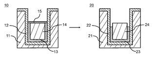
- FIG. 2 is a schematic view of applying the composition for cleaning a semiconductor substrate of the present invention to a semiconductor substrate for memory elements.
- FIG. 2 is a schematic view showing the case where the semiconductor substrate cleaning composition of the present invention is applied to a semiconductor substrate for logic elements.
- a semiconductor substrate cleaning composition according to the present invention comprises (A) an oxidizing agent, (B) a fluorine compound, (C) a metallic tungsten corrosion inhibitor, and (D) a tungsten oxide etching accelerator.
- the addition rate of the (A) oxidizing agent is 0.0001 to 10% by mass with respect to the total mass of the semiconductor substrate cleaning composition
- the addition rate of the (B) fluorine compound is the above It is 0.005 to 10% by mass with respect to the total mass of the semiconductor substrate cleaning composition
- the addition rate of the (C) metal tungsten anticorrosive agent is, relative to the total mass of the semiconductor substrate cleaning composition, It is 0.0001 to 5% by mass.
- a layer containing at least one of titanium and a titanium alloy contained in a semiconductor substrate is selectively removed while suppressing etching of a layer containing metallic tungsten (W) contained in the semiconductor substrate.
- W metallic tungsten
- the titanium alloy is not particularly limited as long as it is obtained by adding one or more kinds of metallic elements other than titanium or non-metallic elements to titanium and has metallic properties, but titanium and aluminum , oxygen, nitrogen, carbon, molybdenum, vanadium, niobium, iron, chromium, nickel, tin, hafnium, zirconium, palladium, ruthenium, and platinum.
- titanium nitride and titanium oxide are preferable, and titanium nitride is more preferable.
- titanium alloy means that the content of titanium element is 20 atomic % or more with respect to the total atomic weight of the titanium alloy.
- the content of the titanium element in the titanium alloy is preferably 25 atomic weight % or more, more preferably 30 atomic weight %, and more preferably 35 atomic weight %, relative to the total atomic weight of the titanium alloy. 40 to 99.9 atomic weight % is particularly preferred.
- the etching rate of tungsten oxide formed on the surface of the material containing metallic tungsten of the semiconductor substrate is high, and the tungsten oxide can be preferably removed.
- tungsten oxide refers to an oxide formed by oxidizing metallic tungsten, and usually means tungsten oxide (VI) (WO 3 ).
- FIG. 1 is a schematic diagram in the case of applying the semiconductor substrate cleaning composition of the present invention to a semiconductor substrate for memory elements.
- a memory element semiconductor substrate (before cleaning) 10 includes a silicon substrate 11 having a recess, an insulating film 12 made of silicon oxide, a barrier film 13 made of titanium nitride, and a metal tungsten film 14 .
- Such a memory element semiconductor substrate (before cleaning) 10 is obtained by successively forming an insulating film made of silicon oxide, a barrier film made of titanium nitride, and a metallic tungsten film on a silicon substrate having recesses, followed by CMP (chemical mechanical polishing).
- the memory element semiconductor substrate (before cleaning) 10 has tungsten oxide 15 formed by oxidizing metal tungsten on the barrier film 13 and the metal tungsten film 14 . Therefore, even if an attempt is made to selectively etch the barrier film 13 made of titanium nitride using the composition for cleaning a semiconductor substrate, the tungsten oxide exists in a form covering the surface of the barrier film 13. The composition may not be able to contact the barrier film 13 and etch the barrier film 13 .
- the tungsten oxide 15 can be preferably removed because the etching rate of tungsten oxide is high. can be done. Therefore, the composition for cleaning a semiconductor substrate of the present invention can come into contact with the barrier film 13 made of titanium nitride, and can selectively etch the barrier film with a high Ti/W etching selectivity. As a result, a memory element semiconductor substrate (after cleaning) is formed by laminating a silicon substrate 21 having a recess, an insulating film 22 made of silicon oxide, an etched barrier film 23 made of titanium nitride, and a metallic tungsten film 24 . ) 20 can be produced.
- FIG. 2 is a schematic diagram in the case of applying the semiconductor substrate cleaning composition of the present invention to a semiconductor substrate for logic elements.
- a semiconductor substrate for logic elements before cleaning 30
- a state after formation of via holes is shown.
- a logic element semiconductor substrate (before cleaning) 30 is arranged on an insulating film 32 made of silicon oxide formed on a silicon substrate (not shown) having a transistor, and on the insulating film 32 . It has a patterned titanium nitride hard mask 33 and metal tungsten plugs 34 located in the insulating layer 32 .
- Such a logic element semiconductor substrate (before cleaning) 30 can be manufactured by the following method.
- a hard mask made of titanium nitride and a resist film are formed on a laminate of a silicon substrate having a transistor and a metal tungsten plug and an insulating layer, and a pattern is formed in the resist film by exposure and development.
- a hard mask pattern is formed by dry etching, and the resist film is removed.
- the logic element semiconductor substrate (before cleaning) 30 has a tungsten oxide 35 formed by oxidizing metal tungsten on the metal tungsten plug 34 .
- the presence of tungsten oxide 35 on the surface of the metal tungsten plug 34 may increase the electric resistance of the metal tungsten plug 34 .
- the semiconductor substrate cleaning composition of the present invention When the semiconductor substrate cleaning composition of the present invention is applied to the logic element semiconductor substrate (before cleaning) 30 having such a structure, the Ti/W etching selectivity is high. Can be selectively removed. Further, since the semiconductor substrate cleaning composition of the present invention has a high etching rate for tungsten oxide, it can also remove tungsten oxide 35 . As a result, a logic element semiconductor substrate (not shown) having an insulating film 42 made of silicon oxide formed on a silicon substrate (not shown) having a transistor and a metal tungsten plug 44 disposed in the insulating film 42 is formed. after washing) 40 can be produced.
- the oxidizing agent has a function of changing the oxidation number of titanium in titanium or a titanium alloy to tetravalent and dissolving it in the semiconductor substrate cleaning composition.
- the oxidizing agent is not particularly limited, but includes peracids, halogen oxoacids, and salts thereof.
- peracid examples include hydrogen peroxide, persulfuric acid, percarbonic acid, superphosphoric acid, peracetic acid, perbenzoic acid, and meta-chloroperbenzoic acid.
- halogen oxoacid examples include chlorine oxoacids such as hypochlorous acid, chlorous acid, chloric acid and perchloric acid; oxoacids of iodine such as hypoiodous acid, iodous acid, iodic acid, and periodic acid;
- the salts include alkali metal salts such as lithium salt, sodium salt, potassium salt, rubidium salt and cesium salt of the above peracid or halogen oxoacid; beryllium salt, magnesium salt and calcium salt of the above peracid or halogen oxoacid; alkaline earth metal salts such as strontium salts and barium salts; metal salts such as aluminum salts, copper salts, zinc salts and silver salts of the above peracids or halogen oxoacids; and ammonium salts of the above peracids or halogen oxoacids. be done.
- alkali metal salts such as lithium salt, sodium salt, potassium salt, rubidium salt and cesium salt of the above peracid or halogen oxoacid
- beryllium salt, magnesium salt and calcium salt of the above peracid or halogen oxoacid alkaline earth metal salts such as strontium salts and barium salts
- the above-mentioned (A) oxidizing agent is preferably hydrogen peroxide or iodine oxoacid, more preferably hydrogen peroxide , iodic acid or periodic acid. Hydrogen peroxide and iodic acid are more preferable, and iodic acid is particularly preferable, since the /W etching selectivity is increased.
- the above (A) oxidizing agent may be used alone or in combination of two or more. That is, in one embodiment, the oxidizing agent (A) preferably contains at least one selected from the group consisting of peracids, halogen oxoacids, and salts thereof, and hydrogen peroxide and iodine oxoacids more preferably at least one selected from the group consisting of hydrogen peroxide, iodic acid, more preferably at least one selected from the group consisting of periodic acid, from hydrogen peroxide, iodic acid It is particularly preferred to contain at least one selected from the group consisting of, most preferably iodic acid.
- the addition rate of the oxidizing agent is 0.0001 to 10% by mass, preferably 0.001 to 5% by mass, more preferably 0, based on the total mass of the semiconductor substrate cleaning composition. 0.003 to 3% by mass, more preferably 0.01 to 2% by mass.
- the addition rate of the oxidizing agent is within the above range from the viewpoint of increasing the WO 3 /W etching selectivity and the Ti/W etching selectivity.
- the fluorine compound has a function of promoting etching of titanium or a titanium alloy.
- the (B) fluorine compound is not particularly limited, but hydrogen fluoride (HF), tetrafluoroboric acid (HBF 4 ), hexafluorosilicic acid (H 2 SiF 6 ), hexafluorozirconic acid (H 2 ZrF 6 ), hexafluorotitanic acid (H 2 TiF 6 ), hexafluorophosphoric acid (HPF 6 ), hexafluoroaluminic acid (H 2 AlF 6 ), hexafluorogermanic acid (H 2 GeF 6 ), and salts thereof. be done.
- the salts include ammonium fluoride (NH 4 F), ammonium tetrafluoroborate (NH 4 BF 4 ), ammonium hexafluorosilicate ((NH 4 ) 2 SiF 6 ), and tetramethyl tetrafluoroborate.
- Ammonium salts such as ammonium (N(CH 3 ) 4 BF 4 ) are included.
- the fluorine compound (B) is preferably hydrogen fluoride (HF), tetrafluoroboric acid (HBF 4 ), hexafluorosilicic acid (H 2 SiF 6 ), and salts thereof.
- Hydrogen (HF), ammonium fluoride (NH 4 F), and hexafluorosilicic acid (H 2 SiF 6 ) are more preferable, since they increase the WO 3 /W etching selectivity and the Ti/W etching selectivity.
- Hydrogen fluoride (HF) is more preferred.
- the above-mentioned (B) fluorine compound may be used individually, or may be used in combination of 2 or more types. That is, in a preferred embodiment, (B) the fluorine compound is hydrogen fluoride (HF), tetrafluoroboric acid (HBF 4 ), hexafluorosilicic acid (H 2 SiF 6 ), hexafluorozirconic acid (H 2 ZrF 6 ), hexafluorotitanic acid (H 2 TiF 6 ), hexafluorophosphoric acid (HPF 6 ), hexafluoroaluminic acid (H 2 AlF 6 ), hexafluorogermanic acid (H 2 GeF 6 ), and salts thereof preferably contains at least one selected from the group consisting of hydrogen fluoride (HF), tetrafluoroboric acid ( HBF4 ), hexafluorosilicic acid ( H2SiF6 ), and salts thereof more preferably at least one
- the addition rate of the fluorine compound is 0.005 to 10% by mass, preferably 0.01 to 5% by mass, more preferably 0, based on the total mass of the semiconductor substrate cleaning composition. 0.03 to 3% by mass, more preferably 0.03 to 1% by mass. It is preferable that the addition rate of the fluorine compound is within the above range from the viewpoints of improving the etching rate of titanium and titanium alloys and increasing the Ti/W etching selectivity.
- the metal tungsten anticorrosive agent adsorbs to metal tungsten to form a protective film, and has a function of preventing or suppressing etching by the semiconductor substrate cleaning composition.
- the (C) metal tungsten corrosion inhibitor is not particularly limited, but includes an ammonium salt represented by the following formula (1), a heteroaryl salt having an alkyl group having 5 to 30 carbon atoms, and the like.
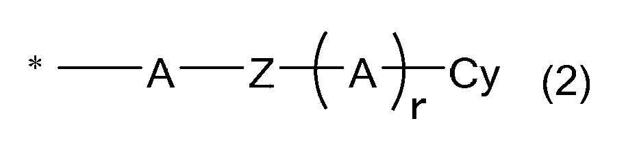
- R 1 is an alkyl group having 5 to 30 carbon atoms, a substituted or unsubstituted alkyl (poly)heteroalkylene group, a substituted or unsubstituted aryl (poly)heteroalkylene group, the following formula (2):
- Cy is a substituted or unsubstituted (hetero)cycloalkyl group, a substituted or unsubstituted (hetero)aryl group, and A each independently has 1 to 5 carbon atoms.
- the alkyl group having 5 to 30 carbon atoms is not particularly limited, but is pentyl group, hexyl group, heptyl group, octyl group, nonyl group, decyl group, undecyl group, dodecyl group, tridecyl group, tetradecyl group, pentadecyl group and hexadecyl. group, heptadecyl group, octadecyl group, nonadecyl group, icosyl group and the like.
- An alkyl(poly)heteroalkylene group is represented by —(C n H 2n —Z—) m —R 3 .
- each n is independently 1 to 5, preferably 1 to 3, more preferably 1 to 2.
- m is 1-5, preferably 1-2.
- Each Z is independently an oxygen atom (O), a sulfur atom (S) or a phosphorus atom (P), preferably an oxygen atom (O).
- R 3 is an alkyl group having 1 to 30 carbon atoms, a methyl group, an ethyl group, a propyl group, an isopropyl group, a butyl group, a pentyl group, a hexyl group, a heptyl group, an octyl group, a nonyl group, a decyl group, and an undecyl group; , dodecyl group, tridecyl group, tetradecyl group, pentadecyl group, hexadecyl group, heptadecyl group, octadecyl group, nonadecyl group, icosyl group and the like.
- the alkyl(poly)heteroalkylene group may have a substituent.
- substituents are usually substituted for the hydrogen atoms of R3.
- the substituent is not particularly limited, but an aryl group having 6 to 20 carbon atoms such as a phenyl group and a naphthyl group; Alkoxy groups of numbers 1 to 6; hydroxy groups; cyano groups; and nitro groups.
- the number of substituents may be one, or two or more may be provided.
- An aryl(poly)heteroalkylene group is represented by -(C n H 2n -Z-) m -Ar.
- each n is independently 1 to 5, preferably 1 to 3, more preferably 1 to 2.
- m is 1-5, preferably 1-2.
- Each Z is independently an oxygen atom (O), a sulfur atom (S) or a phosphorus atom (P), preferably an oxygen atom (O).
- Ar is an aryl group having 6 to 18 carbon atoms, such as a phenyl group, a naphthyl group and an anthracenyl group.
- the aryl(poly)heteroalkylene group may have a substituent.
- the said substituent usually replaces a hydrogen atom of Ar.
- the substituent is not particularly limited, but a methyl group, an ethyl group, a propyl group, an isopropyl group, a butyl group, a 1,1-dimethylbutyl group, a 2,2 - Alkyl groups having 1 to 10 carbon atoms such as dimethylbutyl group and 1,1,3,3-tetramethylbutyl group; alkoxy groups having 1 to 6 carbon atoms such as methoxy, ethoxy and propyloxy groups; hydroxy group; cyano group; nitro group and the like.
- the number of substituents may be one, or two or more may be provided.
- Cy is a substituted or unsubstituted cycloalkyl group having 3 to 10 carbon atoms, a substituted or unsubstituted heterocycloalkyl group having 2 to 10 carbon atoms, a substituted or unsubstituted 6 to 15 carbon atoms is an aryl group, a substituted or unsubstituted heteroaryl group having 2 to 15 carbon atoms, and the cycloalkyl group having 3 to 10 carbon atoms is not particularly limited, but cyclopropyl group, cyclobutyl group, cyclopentyl group, cyclohexyl and the like.
- heterocycloalkyl group having 2 to 10 carbon atoms examples include, but are not limited to, pyrrolidinyl, piperidyl, tetrahydrofuranyl, tetrahydropyranyl, and tetrahydrothienyl groups.
- aryl group having 6 to 15 carbon atoms examples include, but are not particularly limited to, a phenyl group.
- the heteroaryl group having 2 to 15 carbon atoms is not particularly limited, but pyrrolyl group, imidazolyl group, pyrazolyl group, oxazolyl group, isoxazolyl group (isoxazolyl group), thiazolyl group, isothiazolyl group, pyridyl group, pyrazyl group, pyridazyl group, pyrimidyl group, quinolyl group, isoquinolyl group, and the like.
- Each A is independently an alkylene having 1 to 5 carbon atoms.
- the alkylene having 1 to 5 carbon atoms is not particularly limited, but methylene ( --CH.sub.2--), ethylene ( --C.sub.2H.sub.4--), propylene ( --C.sub.3H.sub.6-- ) , isopropylene (--CH(CH 3 ) CH 2 -) and the like.
- r is 0 or 1.
- one or two of the hydroxy groups possessed by the structure derived from monophosphate or diphosphate may be in the form of anions. Specifically, it may have the following structure.
- formula (1) may not have an ammonium salt X 1 ⁇ because a counterion of an ammonium cation will be present in R 1 .
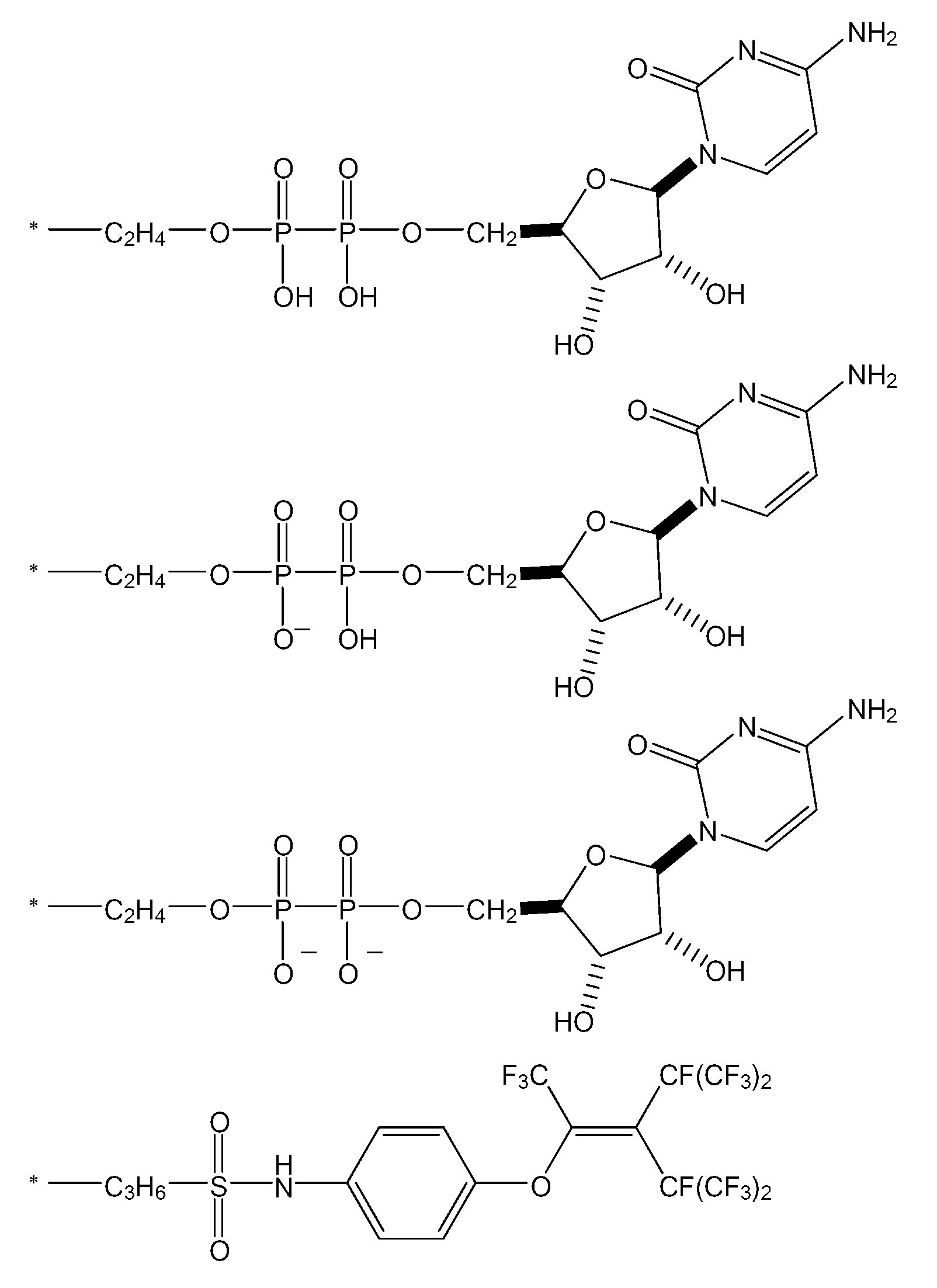
- the group represented by formula (2) preferably includes the following structures.
- R 1 is preferably an alkyl group having 6 to 20 carbon atoms, a substituted or unsubstituted aryl(poly)oxyalkylene group, an alkyl group having 8 to 18 carbon atoms, a substituted or unsubstituted phenyl (Poly)oxyalkylene groups are more preferred, and octyl, decyl, dodecyl, tetradecyl, hexadecyl, octadecyl, phenyloxyethyl (Ph—O—C 2 H 4 —) groups, phenyldi(oxy ethylene) (Ph—(O—C 2 H 4 ) 2 —) group, p-(1,1,3,3-tetramethylbutyl)phenyldi(oxyethylene) (p—CH 3 C(CH 3 ) 2 CH 2 C(CH 3 ) 2 -Ph-(O-C 2 H 4 ) 2 -) group
- Each R 2 is independently a substituted or unsubstituted alkyl group having 1 to 18 carbon atoms or a substituted or unsubstituted aryl group having 6 to 20 carbon atoms.
- the alkyl group having 1 to 18 carbon atoms is not particularly limited, but may be methyl group, ethyl group, propyl group, isopropyl group, butyl group, isobutyl group, sec-butyl group, tert-butyl group, pentyl group, hexyl group, heptyl group, octyl group, nonyl group, decyl group, dodecyl group, tetradecyl group, hexadecyl group, octadecyl group and the like.
- the substituent includes an aryl group having 6 to 20 carbon atoms such as phenyl group and naphthyl group; alkoxy group; hydroxy group; cyano group; nitro group and the like.
- the aryl group having 6 to 20 carbon atoms is not particularly limited, but includes phenyl group, naphthyl group, biphenyl group and the like.
- the substituent include alkyl groups having 1 to 10 carbon atoms such as methyl group, ethyl group, propyl group and isopropyl group; methoxy, ethoxy, propyloxy group and the like. an alkoxy group having 1 to 6 carbon atoms; a hydroxy group; a cyano group; and a nitro group.
- R 2 is preferably a substituted or unsubstituted alkyl group having 1 to 18 carbon atoms, such as a methyl group, an ethyl group, a propyl group, an isopropyl group, a hexyl group, an octyl group, a decyl group, and a dodecyl group.
- R 2 is preferably an alkyl group having 1 to 10 carbon atoms substituted with an aryl group having 6 to 20 carbon atoms, and is more preferably an alkyl group of, more preferably a benzyl group or a phenylethyl group, and particularly preferably a benzyl group.
- the X is a halide ion (fluoride ion, chloride ion, bromide ion, iodide ion, etc.), hydroxide ion, organic sulfonate ion (methanesulfonate ion, p-toluenesulfonate ion, etc.), tetra fluoroborate, hexafluorophosphate and the like.
- X is preferably a halide ion, more preferably a chloride ion or a bromide ion.
- ammonium salts having an alkyl group having 5 to 30 carbon atoms include ammonium salts having a hexyl group such as hexyltrimethylammonium bromide; ammonium salts having a heptyl group such as tetraheptylammonium bromide; octyltrimethylammonium chloride, octyl ammonium salts having an octyl group such as dimethylbenzylammonium chloride; ammonium salts having a decyl group such as decyltrimethylammonium chloride and decyldimethylbenzylammonium chloride; dodecyltrimethylammonium chloride, dodecyltrimethylammonium bromide, dodecylethyldimethylammonium chloride, dodecylethyl Ammonium salts having a dodecyl group such as dimethylammonium bromide, benzyl
- ammonium salts having a substituted or unsubstituted alkyl(poly)heteroalkylene group include trimethylpropyldi(oxyethylene)ammonium chloride and trimethylpropyloxyethylenethioethyleneammonium chloride.
- ammonium salts having a substituted or unsubstituted aryl(poly)heteroalkylene group include trimethyl-2- ⁇ 2-[4-(1,1,3,3-tetramethylbutyl)phenoxy]ethoxy ⁇ ethyl ammonium chloride, benzyldimethyl-2- ⁇ 2-[4-(1,1,3,3-tetramethylbutyl)phenoxy]ethoxy ⁇ ethylammonium chloride (benzethonium chloride), benzyldimethylphenyldi(oxyethylene)ammonium chloride, etc. is mentioned.
- ammonium salts having a group represented by formula (2) include compounds represented by the following structures.
- heteroaryl salt having an alkyl group having 5 to 30 carbon atoms is not particularly limited, but at least one nitrogen atom of a substituted or unsubstituted nitrogen atom-containing heteroaryl ring is bonded to an alkyl group having 5 to 30 carbon atoms. and salts of heteroaryl cations comprising:
- the nitrogen atom-containing heteroaryl ring is not particularly limited, but includes rings such as imidazole, pyrazole, oxazole, isoxazole (isoxazole), thiazole, isothiazole, pyridine, pyrazine, pyridazine, pyrimidine, quinoline, and isoquinoline.
- the substituent includes an alkyl group having 1 to 4 carbon atoms such as methyl group, ethyl group, propyl group and isopropyl group; and 6 carbon atoms such as phenyl group and naphthyl group.
- the alkyl group having 5 to 30 carbon atoms is not particularly limited, but is pentyl group, hexyl group, heptyl group, octyl group, nonyl group, decyl group, undecyl group, dodecyl group, tridecyl group, tetradecyl group, pentadecyl group and hexadecyl. group, heptadecyl group, octadecyl group, nonadecyl group, icosyl group and the like.
- the alkyl group having 5 to 30 carbon atoms is preferably an alkyl group having 6 to 20 carbon atoms, more preferably an alkyl group having 8 to 18 carbon atoms, octyl group, decyl group, dodecyl tetradecyl group, hexadecyl group and octadecyl group are more preferred, decyl group, dodecyl group, tetradecyl group, hexadecyl group and octadecyl group are particularly preferred, and tetradecyl group, hexadecyl group and octadecyl group are particularly preferred. Most preferred.
- the counter anion of the heteroaryl cation having an alkyl group having 5 to 30 carbon atoms is not particularly limited, but includes halide ions such as fluoride ion, chloride ion, bromide ion and iodide ion; hydroxide ion; methanesulfonic acid. ions, organic sulfonate ions such as p-toluenesulfonate ions; tetrafluoroborate; hexafluorophosphate and the like.
- the counter anion is preferably a halide ion, more preferably a chloride ion or a bromide ion.
- heteroaryl salts having an alkyl group having 5 to 30 carbon atoms include 1-methyl-3-hexylimidazolium chloride, 1-octyl-3-methylimidazolium chloride and 1-octyl-3-methylimidazolium.
- pyridinium salts 1-hexylpyrimidinium chloride, 1-hexylpyrimidinium hexafluorophosphate, 1-octylpyrimidinium chloride, 1-decylpyrimidinium chloride, 1-dodecylpyrimidinium chloride, 1-tetradecyl pyrimidinium chloride, pyrimidinium salts such as 1-hexadecylpyrimidinium chloride; dodecylquinolinium chloride, dodecylquinolinium bromide , tetradecylquinolinium chloride, hexadecylquinolinium chloride and the like; dodecylisoquinolinium chloride, dodecylisoquinolinium bromide, tetradecylisoquinolinium chloride, hexadecylisoquinolinium chloride, etc. and isoquinolinium salts. Furthermore, these may be used as hydrates.
- the metal tungsten anticorrosive agent is a pyridinium salt having an alkyl group having 5 to 30 carbon atoms and an ammonium salt represented by the formula (1) (here and R 1 is an alkyl group having 6 to 20 carbon atoms, and R 2 is a substituted or unsubstituted alkyl group having 1 to 18 carbon atoms), a substituted or unsubstituted aryl (poly)heteroalkylene group and from the viewpoint of high etching rate of WO3 , a pyridinium salt having an alkyl group having 14 to 20 carbon atoms, an ammonium salt represented by formula (1) (where R 1 is , an alkyl group having 14 to 20 carbon atoms, and R 2 is a substituted or unsubstituted alkyl group having 1 to 18 carbon atoms), an ammonium salt having a substituted or unsubstituted phenyl (poly)oxyalkylene group More preferably
- the above-mentioned (C) metal tungsten corrosion inhibitor may be used individually, or may be used in combination of 2 or more types. That is, in a preferred embodiment, (C) the metal tungsten anticorrosive is a pyridinium salt having an alkyl group having 5 to 30 carbon atoms, represented by formula (1), from the viewpoint of a high WO 3 /W etching selectivity.
- ammonium salts (wherein R 1 is an alkyl group having 6 to 20 carbon atoms and R 2 is a substituted or unsubstituted alkyl group having 1 to 18 carbon atoms), and substituted or unsubstituted aryl ( It preferably contains at least one selected from the group consisting of ammonium salts having a poly)heteroalkylene group, and from the viewpoint of a high etching rate of WO3 , a pyridinium salt having an alkyl group having 14 to 20 carbon atoms, the formula ( 1) (wherein R 1 is an alkyl group having 14 to 20 carbon atoms and R 2 is a substituted or unsubstituted alkyl group having 1 to 18 carbon atoms), and substituted or more preferably contains at least one selected from the group consisting of ammonium salts having an unsubstituted phenyl (poly)oxyalkylene group, 1-tetradecylpyridinium salt, 1-hexadec
- the addition rate of the metal tungsten corrosion inhibitor is 0.0001 to 5% by mass, preferably 0.001 to 1% by mass, more preferably 0.001 to 1% by mass, based on the total mass of the semiconductor substrate cleaning composition. is 0.003 to 0.5% by mass, more preferably 0.004 to 0.08% by mass.
- the addition rate of the metal tungsten anticorrosive agent is within the above range from the viewpoint of reducing the etching rate of tungsten.
- Tungsten oxide etching accelerator has a function of accelerating the etching of tungsten oxide.
- the (D) tungsten oxide etching accelerator is not particularly limited, but hydrogen chloride, hydrogen bromide, hydrogen iodide, sulfuric acid, nitric acid, methanesulfonic acid, trifluoromethanesulfonic acid, benzenesulfonic acid, p-toluenesulfonic acid , 10-camphorsulfonic acid, and salts thereof.
- the salt includes ammonium salts such as ammonium chloride, ammonium bromide, ammonium iodide, ammonium sulfate, and ammonium nitrate; methylamine hydrochloride, dimethylamine hydrochloride, dimethylamine hydrobromide, methylamine sulfate, etc. and alkylammonium salts of.
- the salt is preferably an ammonium salt.
- (D) tungsten oxide etching accelerator is hydrogen chloride, hydrogen bromide, hydrogen iodide, sulfuric acid, nitric acid, trifluoromethanesulfonic acid, benzenesulfonic acid, p-toluenesulfonic acid, and salts thereof more preferably hydrogen chloride, hydrogen bromide, hydrogen iodide, sulfuric acid, nitric acid, trifluoromethanesulfonic acid, benzenesulfonic acid, p-toluenesulfonic acid, and ammonium salts thereof; Hydrogen chloride, hydrogen iodide, sulfuric acid, nitric acid, ammonium sulfate, ammonium nitrate, methanesulfonic acid, trifluoromethanesulfonic acid, benzenesulfonic acid, and p-toluenesulfonic acid are more preferable, and can maintain a high Ti/W
- hydrogen chloride, hydrogen bromide, hydrogen iodide, sulfuric acid, nitric acid, methanesulfonic acid, trifluoromethanesulfonic acid, benzenesulfonic acid, and p-toluenesulfonic acid are particularly preferred, and hydrogen chloride, hydrogen bromide, More preferred are hydrogen iodide, sulfuric acid, nitric acid and methanesulfonic acid, and most preferred are sulfuric acid and nitric acid.
- (D) tungsten oxide etching accelerator may be used alone or in combination of two or more.
- the tungsten oxide etch accelerator is hydrogen chloride, hydrogen bromide, hydrogen iodide, sulfuric acid, nitric acid, methanesulfonic acid, trifluoromethanesulfonic acid, benzenesulfonic acid, p-toluenesulfone.
- Acid, 10-camphorsulfonic acid and preferably contains at least one selected from the group consisting of salts thereof, hydrogen chloride, hydrogen bromide, hydrogen iodide, sulfuric acid, nitric acid, ammonium chloride, ammonium bromide, More preferably, at least one selected from the group consisting of ammonium iodide, ammonium sulfate, ammonium nitrate, methanesulfonic acid, trifluoromethanesulfonic acid, benzenesulfonic acid, p-toluenesulfonic acid, and 10-camphorsulfonic acid, Hydrogen chloride, hydrogen bromide, hydrogen iodide, sulfuric acid, nitric acid, methanesulfonic acid, trifluoromethanesulfonic acid, benzenesulfonic acid, and p-toluenesulfonic acid. , hydrogen bromide, hydrogen iodide, sulfuric acid and
- the addition rate of the tungsten oxide etching accelerator is preferably 0.01 to 20% by mass, more preferably 0.03 to 10% by mass, based on the total mass of the semiconductor substrate cleaning composition. It is more preferably 0.05 to 8% by mass, particularly preferably 0.1 to 3% by mass, and most preferably 0.1 to 0.8% by mass. (D) It is preferable that the addition rate of the tungsten oxide etching accelerator is within the above range because the tungsten oxide removal rate can be increased while maintaining the Ti/W etching selectivity.
- the semiconductor substrate cleaning composition may contain a pH adjuster as necessary. Acids and alkalis other than (A) the oxidizing agent, (B) the fluorine compound, and (D) the tungsten oxide etching accelerator can be used as the pH adjuster. Organic acids and inorganic acids can be used as the acid. Organic alkalis and inorganic alkalis can be used as alkalis. Ammonia is preferred as the pH adjuster.
- the semiconductor substrate cleaning composition preferably contains a solvent.
- the solvent has a function of uniformly dispersing each component contained in the semiconductor substrate cleaning composition, a function of diluting it, and the like.
- Examples of the solvent include water and organic solvents.
- the water is not particularly limited, but it is preferably water from which metal ions, organic impurities, particles, etc. have been removed by distillation, ion exchange treatment, filter treatment, various adsorption treatments, etc. Pure water is preferred. More preferably, ultrapure water is particularly preferred.
- the organic solvent is not particularly limited, but alcohols such as methanol, ethanol, 1-propanol, 2-propanol, 1-butanol, tert-butanol; ethylene glycol, propylene glycol, neopentyl glycol, 1,2-hexanediol.
- alcohols such as methanol, ethanol, 1-propanol, 2-propanol, 1-butanol, tert-butanol; ethylene glycol, propylene glycol, neopentyl glycol, 1,2-hexanediol.
- the solvent is water.
- the said solvent may be used individually or may be used in combination of 2 or more type.
- the addition rate of the solvent, particularly water is preferably 50% by mass or more, more preferably 80% by mass or more, and 90% by mass or more, relative to the total mass of the semiconductor substrate cleaning composition. is more preferably 95% by mass or more, and particularly preferably 95% by mass or more.
- a solvent addition rate of 50% by mass or more is preferable from the viewpoint that the Ti/W etching selection ratio and the WO 3 /W etching selection ratio can be suitably controlled.
- the semiconductor substrate cleaning composition preferably further contains an iodine scavenger.
- the iodine scavenger is not particularly limited, but acetone, butanone, 2-methyl-2-butanone, 3,3-dimethyl-2-butanone, 4-hydroxy-2-butanone, 2-pentanone, 3-pentanone, 3 -methyl-2-pentanone, 4-methyl-2-pentanone, 2-methyl-3-pentanone, 5-methyl-3-pentanone, 2,4-dimethyl-3-pentanone, 5-hydroxy-2-pentanone, 4 -hydroxy-4-methyl-2-pentanone, 2-hexanone, 3-hexanone, 2-heptanone, 3-heptanone, 4-heptanone, 5-methyl-2-heptanone, 5-methyl-3-heptanone, 2,6 -aliphatic ketones such as dimethyl-4-heptanone, 2-octanone, 3-octanone, 4-octanone, cyclohexanone, 2,6-dimethylcyclohexanone, 2-acetyl
- the semiconductor substrate cleaning composition may further contain a low dielectric passivator.
- a low dielectric constant passivating agent has a function of preventing or suppressing etching of a low dielectric constant film such as an insulating film.
- low dielectric constant passivating agent examples include, but are not limited to, boric acid; borates such as ammonium pentaborate and sodium tetraborate; carboxylic acids such as 3-hydroxy-2-naphthoic acid, malonic acid and iminodiacetic acid. mentioned.
- These low dielectric constant passivating agents may be used alone or in combination of two or more.
- the addition rate of the low dielectric constant passivating agent is preferably 0.01 to 2% by mass, more preferably 0.02 to 1% by mass, relative to the total mass of the semiconductor substrate cleaning composition. More preferably, it is 0.03 to 0.5% by mass.
- the semiconductor substrate cleaning composition may further contain additives.
- additives include surfactants, chelating agents, antifoaming agents, silicon-containing compounds, and the like.
- the pH of the semiconductor substrate cleaning composition is preferably 0.1 to 5.0, more preferably 0.1 to 3 from the viewpoint of increasing the Ti/W etching selectivity, and 0.2. It is more preferably from 0.2 to 2, even more preferably from 0.3 to 1.8, and particularly preferably from 0.4 to 1.5.
- the etching rate of tungsten oxide in the semiconductor substrate cleaning composition is preferably 2.0 ⁇ /min or more, more preferably 2.2 ⁇ /min or more, and further preferably 2.5 ⁇ /min or more. It is preferably 3.0 to 50 ⁇ /min, most preferably 3.5 to 30 ⁇ /min.
- An etching rate of tungsten oxide of 2.0 ⁇ /min or more is preferable from the viewpoint of shortening the time required for the selective etching step of titanium/titanium alloy and increasing the WO 3 /W etching selectivity. .
- the etching rate of tungsten oxide means the value measured by the method of the example.
- the etching rate of metallic tungsten in the semiconductor substrate cleaning composition is preferably 7.5 ⁇ /min or less, more preferably 5.0 ⁇ /min or less, and further preferably 4.5 ⁇ /min or less. It is preferably 4.0 ⁇ /min or less, and most preferably 0.1 to 3.5 ⁇ /min. It is preferable that the etching rate of metallic tungsten is 7.5 ⁇ /min or less because the Ti/W etching selectivity ratio is high. In addition, the etching rate of metal tungsten means the value measured by the method of an Example.
- the etching rate of titanium and titanium alloys in the cleaning composition for semiconductor substrates is preferably 7 ⁇ /min or more, more preferably 9 ⁇ /min or more, further preferably 15 ⁇ /min or more, further preferably 30 ⁇ /min. min or more, particularly preferably 50 ⁇ /min or more, and most preferably 80 ⁇ /min or more. It is preferable that the etching rate of the titanium alloy is 7 ⁇ /min or more because the Ti/W etching selectivity ratio is high.
- the etching rate of titanium and titanium alloy means the value measured by the method of the example.
- the etching rate of the insulating layer material of the semiconductor substrate cleaning composition is preferably 3.0 ⁇ /min or less, more preferably 1.0 ⁇ /min or less, and preferably 0.7 ⁇ /min or less. It is more preferably 0.6 ⁇ /min or less, particularly preferably 0.5 ⁇ /min or less, and most preferably 0.5 ⁇ /min or less. It is preferable that the etching rate of the insulating layer material is 3.0 ⁇ /min or less because the shape of the semiconductor substrate is maintained and the performance as a semiconductor device is enhanced.
- the insulating layer material is not particularly limited, but includes silicon oxide (eg, th-Ox). The etching rate of the insulating layer material means the value measured by the method of the example.
- the Ti/W etching selectivity ratio (titanium and titanium alloy etching rate/tungsten metal etching rate) of the semiconductor substrate cleaning composition is preferably 5 or more, more preferably 10 or more, and 20 or more. It is more preferably 1, particularly preferably 30 or more, and most preferably 50 or more. A Ti/W etching selectivity of 5 or more is preferable because a desired etching manufacturing process can be established.
- the WO 3 /W etching selectivity (tungsten oxide etching rate/tungsten metal etching rate) of the semiconductor substrate cleaning composition is preferably 0.5 or more, more preferably 0.8 or more. It is more preferably 1.0 or more, particularly preferably 1.5-15, and most preferably 3-10. A WO 3 /W etching selection ratio of 0.5 or more is preferable because productivity increases. That is, according to a preferred embodiment, there is provided a semiconductor substrate cleaning composition for etching tungsten oxide while suppressing etching of metallic tungsten.
- a method for cleaning a semiconductor substrate using the composition for cleaning a semiconductor substrate described above includes bringing a semiconductor substrate having a layer containing metallic tungsten, a layer containing at least one of titanium and a titanium alloy, and a layer containing tungsten oxide into contact with the composition for cleaning a semiconductor substrate described above. and removing at least a portion of the layer comprising at least one of titanium and titanium alloys and the layer comprising tungsten oxide.
- the configuration of the semiconductor substrate before cleaning may differ depending on the application.
- the semiconductor substrate when used for a memory element, it can have a structure in which an insulating film, a barrier film made of titanium or titanium nitride, and a metallic tungsten film are laminated in this order on a silicon substrate having a recess.
- a tungsten oxide film may be formed on the surface of the tungsten metal film by oxidizing the tungsten metal. This tungsten oxide film is produced, for example, by oxidation due to oxygen in the atmosphere, oxidation due to ashing, or the like.
- the layer containing metallic tungsten corresponds to the metallic tungsten film
- the layer containing at least one of titanium and titanium alloy corresponds to the barrier film
- the layer containing tungsten oxide corresponds to the tungsten oxide film.
- an etched insulating film, a patterned hard mask made of titanium or titanium nitride, and an insulating film formed by etching are formed on a silicon substrate having a transistor layer. and metallic tungsten formed at the bottom of the recess in the membrane.
- a tungsten oxide film may be formed on the surface of the tungsten metal by oxidizing the tungsten metal. This tungsten oxide film is produced, for example, by oxidation due to oxygen in the atmosphere, oxidation due to ashing, or the like.
- the layer containing metallic tungsten corresponds to the metallic tungsten formed at the bottom of the recess of the insulating film formed by etching, and the layer containing at least one of titanium and titanium alloy is hard.
- a layer corresponding to a mask and containing tungsten oxide corresponds to a tungsten oxide film.
- the configuration of the semiconductor substrate before cleaning can be changed by appropriately referring to known techniques.
- At least part of the layer containing at least one of titanium and a titanium alloy and the layer containing tungsten oxide can be removed. can. Thereby, tungsten oxide can be removed while selectively etching titanium/titanium alloy.
- the method of contacting the semiconductor substrate with the semiconductor substrate cleaning composition is not particularly limited, and known techniques can be appropriately employed.
- the semiconductor substrate may be immersed in the semiconductor substrate cleaning composition, the semiconductor substrate cleaning composition may be sprayed onto the semiconductor substrate, or the semiconductor substrate may be dripped (single-wafer spin treatment, etc.). good.
- the immersion may be repeated two or more times, the spraying may be repeated two or more times, the dropping may be repeated two or more times, or the immersion, spraying, and dropping may be combined.
- the contact temperature is not particularly limited, it is preferably 0 to 90°C, more preferably 15 to 80°C, and even more preferably 20 to 70°C.
- the contact time is not particularly limited, but is preferably 10 seconds to 3 hours, more preferably 10 seconds to 1 hour, even more preferably 10 seconds to 45 minutes, even more preferably 20 seconds to 5 minutes. It is particularly preferred to have
- a method for manufacturing a semiconductor substrate using the composition for cleaning a semiconductor substrate described above includes bringing a semiconductor substrate having a layer containing metallic tungsten, a layer containing at least one of titanium and a titanium alloy, and a layer containing tungsten oxide into contact with the semiconductor substrate cleaning composition described above. and removing at least a portion of the layer comprising at least one of titanium and titanium alloys and the layer comprising tungsten oxide.
- a semiconductor substrate manufactured in this way can be used as a material for a semiconductor device to manufacture a semiconductor device with high performance.
- Example 1 (A) iodic acid (HIO 3 ) as an oxidizing agent, (B) hydrogen fluoride (HF) as a fluorine compound, (C) 1-dodecylpyridinium chloride (DPC) as a metal tungsten corrosion inhibitor, ( D) Sulfuric acid, which is a tungsten oxide etching accelerator, was added to pure water and stirred to produce a composition for cleaning a semiconductor substrate. At this time, the addition rates of iodic acid, hydrogen fluoride, 1-dodecylpyridinium chloride (DPC), and sulfuric acid were 0.018% by mass and 0.05% by mass, respectively, based on the total mass of the semiconductor substrate cleaning composition.
- HIO 3 iodic acid
- HF hydrogen fluoride
- DPC 1-dodecylpyridinium chloride
- Sulfuric acid which is a tungsten oxide etching accelerator
- the pH of the semiconductor substrate cleaning composition was 1.3.
- the pH of the pretreatment agent was measured at 23° C. using a desktop pH meter (F-71) and a pH electrode (9615S-10D) manufactured by Horiba, Ltd.
- Examples 2 to 19 and Comparative Examples 1 to 8 Compositions for cleaning semiconductor substrates were produced by changing the components to be added as shown in Tables 1 and 2 below.
- DPC, CPC, DMIC, CTAB, HTMAB, and BZC used in Examples and Comparative Examples have the following structures.
- Etching rates of the semiconductor substrate cleaning compositions produced in Examples 1 to 19 and Comparative Examples 1 to 8 for tungsten oxide films, metal tungsten films, titanium nitride films, and silicon oxide (th-Ox) films, and metal tungsten (The etching selectivity of tungsten oxide (WO 3 ) to W) (WO 3 /W etching selectivity) and the etching selectivity of titanium nitride (TiN) to metallic tungsten (W) (TiN/W etching selectivity) were evaluated.
- tungsten oxide (WO 3 ) film A film of tungsten oxide (WO 3 ) is formed on a silicon wafer by physical vapor deposition to a thickness of 3000 ⁇ , and a tungsten oxide film is formed by cutting into a size of 1 cm ⁇ 1 cm (immersion treatment area: 1 cm 2 ). made a sample
- a tungsten oxide film sample was immersed in 10 g of the semiconductor substrate cleaning compositions produced in Examples 1 to 19 and Comparative Examples 1 to 8 at a predetermined treatment temperature for 10 minutes.
- a sample for measurement was prepared by diluting the semiconductor substrate cleaning composition after immersion treatment by 10 to 20 times with a 1% by mass nitric acid aqueous solution.
- the tungsten concentration in the measurement sample was measured using an ICP optical emission spectrometer (ICP-OES) Avio200 (manufactured by PerkinElmer).
- the sample for creating the calibration curve was prepared by the following method. That is, by diluting a tungsten standard solution (tungsten concentration: 1000 ppm, manufactured by FUJIFILM Wako Co., Ltd.) with a 1% by mass nitric acid aqueous solution, the concentration of tungsten is 25 ppb, 12.5 ppb, and for creating calibration curves of 2.5 ppb. A sample was prepared.
- a tungsten standard solution tungsten concentration: 1000 ppm, manufactured by FUJIFILM Wako Co., Ltd.
- 231.84 (g/mol) is the molecular weight of tungsten oxide (WO 3 )
- 7.16 (g/cm 3 ) is the density of tungsten oxide
- 1 cm 2 is the tungsten oxide film.
- 183.84 (g/mol) is the immersion treated area of the sample and is the molecular weight of metallic tungsten (W).
- the etching rate (E.R.) of the tungsten oxide film was calculated by dividing the calculated etching amount of the tungsten oxide film by the immersion treatment time using the semiconductor substrate cleaning composition. The results obtained are shown in Table 3 below.
- a measurement sample was prepared in the same manner as the method for measuring the etching rate of a tungsten oxide film, except that a metal tungsten film sample was used and the immersion treatment time was 2 minutes. Concentration was measured.
- the etching rate (E.R.) of the metallic tungsten film was calculated by dividing the calculated etching amount of the metallic tungsten film by the immersion treatment time using the semiconductor substrate cleaning composition. The results obtained are shown in Table 3 below.
- TiN thickness of silicon nitride
- the film thickness of the titanium nitride film sample was measured using a fluorescent X-ray device EA1200VX (manufactured by Hitachi high-tech).
- a titanium nitride film sample was immersed in 10 g of the semiconductor substrate cleaning compositions produced in Examples 1 to 19 and Comparative Examples 1 to 8 at a predetermined treatment temperature for a predetermined time.
- the film thickness of the titanium nitride film sample after the semiconductor substrate cleaning composition immersion treatment was measured by the same method as above.
- the film thickness difference of the titanium nitride film sample before and after the semiconductor substrate cleaning composition immersion treatment was calculated, and the etching rate of the titanium nitride film (E .R.) was calculated.
- the results obtained are shown in Table 3 below.
- a silicon oxide film was formed to a thickness of 1000 ⁇ by thermal oxidation of a silicon wafer, and a silicon oxide film sample was prepared by cutting into a size of 1 cm ⁇ 1 cm (immersion treatment area: 1 cm 2 ).
- the film thickness of the silicon oxide film sample was measured using an optical film thickness meter n&k1280 (manufactured by n&k Technology).
- a silicon oxide film-forming sample was immersed in 10 g of the semiconductor substrate cleaning compositions produced in Examples 1 to 19 and Comparative Examples 1 to 8 at a predetermined treatment temperature for 30 minutes.
- the film thickness of the silicon oxide film-formed sample after the immersion treatment was measured by the same method as above.
- the etching rate (E.R.) of the silicon oxide film was calculated by calculating the film thickness difference of the silicon oxide film-formed sample before and after the treatment and dividing it by the immersion treatment time using the semiconductor substrate cleaning composition. .
- the results obtained are shown in Table 3 below.
- TiN/W etching selectivity Dividing the etching rate (E.R.) of the titanium nitride film of the semiconductor substrate cleaning compositions produced in Examples 1 to 19 and Comparative Examples 1 to 8 by the etching rate (E.R.) of the metal tungsten film , the TiN/W etching selectivity was calculated. The results obtained are shown in Table 3 below.
- the semiconductor cleaning compositions of Examples 1 to 19 have a high TiN/W etching selectivity.
- the semiconductor cleaning compositions of Examples 1 to 19 have high etching rates for tungsten oxide (WO 3 ), it can be seen that the processing time for removing tungsten oxide can be shortened.
Landscapes
- Chemical & Material Sciences (AREA)
- Life Sciences & Earth Sciences (AREA)
- Engineering & Computer Science (AREA)
- Chemical Kinetics & Catalysis (AREA)
- Oil, Petroleum & Natural Gas (AREA)
- Wood Science & Technology (AREA)
- Organic Chemistry (AREA)
- Inorganic Chemistry (AREA)
- Health & Medical Sciences (AREA)
- Emergency Medicine (AREA)
- Detergent Compositions (AREA)
- Cleaning Or Drying Semiconductors (AREA)
Abstract
Description
前記(A)酸化剤の添加率が、前記半導体基板洗浄用組成物の全質量に対して、0.0001~10質量%であり、
前記(B)フッ素化合物の添加率が、前記半導体基板洗浄用組成物の全質量に対して、0.005~10質量%であり、
前記(C)金属タングステン防食剤の添加率が、前記半導体基板洗浄用組成物の全質量に対して、0.0001~5質量%である、半導体基板洗浄用組成物。
[2]前記(D)酸化タングステンエッチング加速剤の添加率が、前記半導体基板洗浄用組成物の全質量に対して、0.01~20質量%である、上記[1]に記載の半導体基板洗浄用組成物。
[3]前記(A)酸化剤が、過酸、ハロゲンオキソ酸、およびこれらの塩からなる群から選択される少なくとも1つを含む、上記[1]または[2]に記載の半導体基板洗浄用組成物。
[4]前記(B)フッ素化合物が、フッ化水素(HF)、テトラフルオロホウ酸(HBF4)、ヘキサフルオロケイ酸(H2SiF6)、ヘキサフルオロジルコニウム酸(H2ZrF6)、ヘキサフルオロチタン酸(H2TiF6)、ヘキサフルオロリン酸(HPF6)、ヘキサフルオロアルミン酸(H2AlF6)、ヘキサフルオロゲルマン酸(H2GeF6)、およびこれらの塩からなる群から選択される少なくとも1つを含む、上記[1]~[3]のいずれかに記載の半導体基板洗浄用組成物。
[5]前記(C)金属タングステン防食剤が、下記式(1):

R1は、炭素数5~30のアルキル基、置換または非置換のアルキル(ポリ)ヘテロアルキレン基、置換または非置換のアリール(ポリ)ヘテロアルキレン基、下記式(2):
Cyは、置換または非置換の炭素数3~10のシクロアルキル基、置換または非置換の炭素数2~10のヘテロシクロアルキル基、置換または非置換の炭素数6~15のアリール基、置換または非置換の炭素数2~15のヘテロアリール基であり、
Aは、それぞれ独立して、炭素数1~5のアルキレンであり、
rは、0または1であり、
Zは、下記式:

で表される基であり、
R2は、それぞれ独立して、置換または非置換の炭素数1~18のアルキル基、置換または非置換の炭素数6~20のアリール基であり、
Xは、ハロゲン化物イオン、水酸化物イオン、有機スルホン酸イオン、テトラフルオロボレート、ヘキサフルオロフォスファートである。)
で表されるアンモニウム塩および炭素数5~30のアルキル基を有するヘテロアリール塩からなる群から選択される少なくとも1つを含む、上記[1]~[4]のいずれかに記載の半導体基板洗浄用組成物。
[6]前記(D)酸化タングステンエッチング加速剤が、塩化水素、臭化水素、ヨウ化水素、硫酸、硝酸、メタンスルホン酸、トリフルオロメタンスルホン酸、ベンゼンスルホン酸、p-トルエンスルホン酸、10-カンファースルホン酸、およびこれらの塩からなる群から選択される少なくとも1つを含む、上記[1]~[5]のいずれかに記載の半導体基板洗浄用組成物。
[7]前記塩がアンモニウム塩である、上記[6]に記載の半導体基板洗浄用組成物。
[8]pHが、0.1~5.0である、上記[1]~[7]のいずれかに記載の半導体基板洗浄用組成物。
[9]金属タングステンのエッチングを抑制しつつ酸化タングステンをエッチングするための半導体基板洗浄用組成物である、上記[1]~[8]のいずれかに記載の半導体基板洗浄用組成物。
[10]金属タングステンを含む層と、チタンおよびチタン合金の少なくとも1つを含む層と、酸化タングステンを含む層と、を有する半導体基板を、上記[1]~[9]のいずれかに記載の半導体基板洗浄用組成物と接触させて、前記チタンおよびチタン合金の少なくとも1つを含む層および前記酸化タングステンを含む層の少なくとも一部を除去する工程を含む、半導体基板の洗浄方法。
[11]金属タングステンを含む層と、チタンおよびチタン合金の少なくとも1つを含む層と、酸化タングステンを含む層と、を有する半導体基板を、上記[1]~[9]のいずれかに記載の半導体基板洗浄用組成物と接触させて、前記チタンおよびチタン合金の少なくとも1つを含む層および前記酸化タングステンを含む層の少なくとも一部を除去する工程を含む、半導体基板の製造方法。
本発明に係る半導体基板洗浄用組成物は、(A)酸化剤と、(B)フッ素化合物と、(C)金属タングステン防食剤と、(D)酸化タングステンエッチング加速剤と、を含む。この際、前記(A)酸化剤の添加率が、前記半導体基板洗浄用組成物の全質量に対して、0.0001~10質量%であり、前記(B)フッ素化合物の添加率が、前記半導体基板洗浄用組成物の全質量に対して、0.005~10質量%であり、前記(C)金属タングステン防食剤の添加率が、前記半導体基板洗浄用組成物の全質量に対して、0.0001~5質量%である。
(A)酸化剤は、チタンまたはチタン合金中のチタンの酸化数を4価に変化させ、半導体基板洗浄用組成物に溶解させる機能等を有する。
(B)フッ素化合物は、チタンまたはチタン合金のエッチングを促進する機能等を有する。
(C)金属タングステン防食剤は、金属タングステンに吸着して保護膜を形成し、半導体基板洗浄用組成物によるエッチングを防止または抑制する機能等を有する。





(D)酸化タングステンエッチング加速剤は、酸化タングステンのエッチングを加速させる機能を有する。
半導体基板洗浄用組成物は、必要に応じてpH調整剤を含んでいてもよい。前記pH調整剤としては、例えば、前記(A)酸化剤、(B)フッ素化合物、(D)酸化タングステンエッチング加速剤以外の酸、アルカリを用いることができる。前記酸としては、有機酸、無機酸を用いることができる。アルカリとしては、有機アルカリ、無機アルカリを用いることができる。pH調整剤としては、アンモニアが好ましい。
半導体基板洗浄用組成物は、溶媒を含むことが好ましい。前記溶媒は、半導体基板洗浄用組成物中に含まれる各成分を均一に分散させる機能、希釈する機能等を有する。
上記(A)酸化剤がヨウ素のオキソ酸を含む場合には、半導体基板洗浄用組成物は、ヨウ素捕捉剤をさらに含むことが好ましい。
半導体基板洗浄用組成物は、低誘電率不動態化剤をさらに含んでいてもよい。低誘電率不動態化剤は、低誘電率膜、例えば絶縁膜のエッチングを防止または抑制する機能を有する。
半導体基板洗浄用組成物は、添加剤をさらに含んでいてもよい。当該添加剤としては、界面活性剤、キレート剤、消泡剤、ケイ素含有化合物等が挙げられる。
半導体基板洗浄用組成物のpHは、0.1~5.0であることが好ましく、Ti/Wエッチング選択比が高くなる観点から、0.1~3であることがより好ましく、0.2~2であることがさらに好ましく、0.3~1.8であることがことさら好ましく、0.4~1.5であることが特に好ましい。
本発明の一形態によれば、上述した半導体基板洗浄用組成物を用いた半導体基板の洗浄方法が提供される。前記洗浄方法は、金属タングステンを含む層と、チタンおよびチタン合金の少なくとも1つを含む層と、酸化タングステンを含む層と、を有する半導体基板を、上述の半導体基板洗浄用組成物と接触させて、前記チタンおよびチタン合金の少なくとも1つを含む層および前記酸化タングステンを含む層の少なくとも一部を除去する工程を含む。
また、本発明の一形態によれば、上述した半導体基板洗浄用組成物を用いた半導体基板の製造方法が提供される。前記製造方法は、金属タングステンを含む層と、チタンおよびチタン合金の少なくとも1つを含む層と、酸化タングステンを含む層と、を有する半導体基板を、上述の半導体基板洗浄用組成物と接触させて、前記チタンおよびチタン合金の少なくとも1つを含む層および前記酸化タングステンを含む層の少なくとも一部を除去する工程を含む。
(A)酸化剤であるヨウ素酸(HIO3)と、(B)フッ素化合物であるフッ化水素(HF)と、(C)金属タングステン防食剤である1-ドデシルピリジニウムクロリド(DPC)と、(D)酸化タングステンエッチング加速剤である硫酸と、を純水に添加し、撹拌することで、半導体基板洗浄用組成物を製造した。この際、ヨウ素酸、フッ化水素、1-ドデシルピリジニウムクロリド(DPC)、および硫酸の添加率は、それぞれ半導体基板洗浄用組成物の全質量に対して、0.018質量%、0.05質量%、0.005質量%、および0.5質量%であった。また、半導体基板洗浄用組成物のpHは1.3であった。pHは、株式会社堀場製作所製卓上型pHメーター(F―71)とpH電極(9615S-10D)を用いて、23℃における前処理剤のpHを測定した。
下記表1および表2の通りに添加する成分等を変更して、半導体基板洗浄用組成物を製造した。


実施例1~19および比較例1~8で製造した半導体基板洗浄用組成物の酸化タングステン膜、金属タングステン膜、窒化チタン膜、および酸化ケイ素(th-Ox)膜に対するエッチング速度、並びに金属タングステン(W)に対する酸化タングステン(WO3)のエッチング選択性(WO3/Wエッチング選択比)、金属タングステン(W)に対する窒化チタン(TiN)のエッチング選択性(TiN/Wエッチング選択比)を評価した。
シリコンウェハに物理気相成長法にて酸化タングステン(WO3)を厚さ3000Åとなるまで製膜し、1cm×1cm(浸漬処理面積:1cm2)の大きさに切り出すことで、酸化タングステン製膜サンプルを作製した

シリコンウェハに物理気相成長法にてタングステン(W)を厚さ1000Åとなるまで製膜し、1cm×1cm(浸漬処理面積:1cm2)の大きさに切り出すことで、金属タングステン製膜サンプルを作製した

シリコンウェハに物理気相成長法にて窒化チタン(TiN)を厚さ1000Åとなるまで製膜し、2cm×2cm(浸漬処理面積:4cm2)の大きさに切り出すことで、窒化チタン製膜サンプルを作製した。
シリコンウェハの熱酸化により酸化ケイ素を厚さ1000Åとなるまで製膜し、1cm×1cm(浸漬処理面積:1cm2)の大きさに切り出すことで、酸化ケイ素製膜サンプルを作製した。
実施例1~19および比較例1~8で製造した半導体基板洗浄用組成物の酸化タングステン膜のエッチング速度(E.R.)を金属タングステン膜のエッチング速度(E.R.)で除することで、WO3/Wエッチング選択比を算出した。得られた結果を下記表3に示す。
実施例1~19および比較例1~8で製造した半導体基板洗浄用組成物の窒化チタン膜のエッチング速度(E.R.)を金属タングステン膜のエッチング速度(E.R.)で除することで、TiN/Wエッチング選択比を算出した。得られた結果を下記表3に示す。

11 凹部を有するシリコン基板
12 絶縁膜
13 バリア膜
14 金属タングステン膜
15 酸化タングステン
20 メモリ素子用半導体基板(洗浄後)
21 凹部を有するシリコン基板
22 絶縁膜
23 エッチングされたバリア膜
24 金属タングステン膜
30 ロジック素子用半導体基板(洗浄前)
32 絶縁膜
33 ハードマスク
34 金属タングステンプラグ
35 酸化タングステン
40 ロジック素子用半導体基板(洗浄後)
42 絶縁膜
44 金属タングステンプラグ
Claims (11)
- (A)酸化剤と、(B)フッ素化合物と、(C)金属タングステン防食剤と、(D)酸化タングステンエッチング加速剤と、を含む、半導体基板洗浄用組成物であって、
前記(A)酸化剤の添加率が、前記半導体基板洗浄用組成物の全質量に対して、0.0001~10質量%であり、
前記(B)フッ素化合物の添加率が、前記半導体基板洗浄用組成物の全質量に対して、0.005~10質量%であり、
前記(C)金属タングステン防食剤の添加率が、前記半導体基板洗浄用組成物の全質量に対して、0.0001~5質量%である、半導体基板洗浄用組成物。 - 前記(D)酸化タングステンエッチング加速剤の添加率が、前記半導体基板洗浄用組成物の全質量に対して、0.01~20質量%である、請求項1に記載の半導体基板洗浄用組成物。
- 前記(A)酸化剤が、過酸、ハロゲンオキソ酸、およびこれらの塩からなる群から選択される少なくとも1つを含む、請求項1または2に記載の半導体基板洗浄用組成物。
- 前記(B)フッ素化合物が、フッ化水素(HF)、テトラフルオロホウ酸(HBF4)、ヘキサフルオロケイ酸(H2SiF6)、ヘキサフルオロジルコニウム酸(H2ZrF6)、ヘキサフルオロチタン酸(H2TiF6)、ヘキサフルオロリン酸(HPF6)、ヘキサフルオロアルミン酸(H2AlF6)、ヘキサフルオロゲルマン酸(H2GeF6)、およびこれらの塩からなる群から選択される少なくとも1つを含む、請求項1~3のいずれか1項に記載の半導体基板洗浄用組成物。
- 前記(C)金属タングステン防食剤が、下記式(1):

R1は、炭素数5~30のアルキル基、置換または非置換のアルキル(ポリ)ヘテロアルキレン基、置換または非置換のアリール(ポリ)ヘテロアルキレン基、下記式(2):

Cyは、置換または非置換の炭素数3~10のシクロアルキル基、置換または非置換の炭素数2~10のヘテロシクロアルキル基、置換または非置換の炭素数6~15のアリール基、置換または非置換の炭素数2~15のヘテロアリール基であり、
Aは、それぞれ独立して、炭素数1~5のアルキレンであり、
rは、0または1であり、
Zは、下記式:

で表される基であり、
R2は、それぞれ独立して、置換または非置換の炭素数1~18のアルキル基、置換または非置換の炭素数6~20のアリール基であり、
Xは、ハロゲン化物イオン、水酸化物イオン、有機スルホン酸イオン、テトラフルオロボレート、ヘキサフルオロフォスファートである。)
で表されるアンモニウム塩および炭素数5~30のアルキル基を有するヘテロアリール塩からなる群から選択される少なくとも1つを含む、請求項1~4のいずれか1項に記載の半導体基板洗浄用組成物。 - 前記(D)酸化タングステンエッチング加速剤が、塩化水素、臭化水素、ヨウ化水素、硫酸、硝酸、メタンスルホン酸、トリフルオロメタンスルホン酸、ベンゼンスルホン酸、p-トルエンスルホン酸、10-カンファースルホン酸、およびこれらの塩からなる群から選択される少なくとも1つを含む、請求項1~5のいずれか1項に記載の半導体基板洗浄用組成物。
- 前記塩が、アンモニウム塩である、請求項6に記載の半導体基板洗浄用組成物。
- pHが、0.1~5.0である、請求項1~7のいずれか1項に記載の半導体基板洗浄用組成物。
- 金属タングステンのエッチングを抑制しつつ酸化タングステンをエッチングするための半導体基板洗浄用組成物である、請求項1~8のいずれか1項に記載の半導体基板洗浄用組成物。
- 金属タングステンを含む層と、チタンおよびチタン合金の少なくとも1つを含む層と、酸化タングステンを含む層と、を有する半導体基板を、請求項1~9のいずれか1項に記載の半導体基板洗浄用組成物と接触させて、前記チタンおよびチタン合金の少なくとも1つを含む層および前記酸化タングステンを含む層の少なくとも一部を除去する工程を含む、半導体基板の洗浄方法。
- 金属タングステンを含む層と、チタンおよびチタン合金の少なくとも1つを含む層と、酸化タングステンを含む層と、を有する半導体基板を、請求項1~9のいずれか1項に記載の半導体基板洗浄用組成物と接触させて、前記チタンおよびチタン合金の少なくとも1つを含む層および前記酸化タングステンを含む層の少なくとも一部を除去する工程を含む、半導体基板の製造方法。
Priority Applications (5)
| Application Number | Priority Date | Filing Date | Title |
|---|---|---|---|
| US18/276,480 US20240117277A1 (en) | 2021-02-12 | 2022-02-04 | Composition for cleaning semiconductor substrate, method for cleaning semiconductor substrate, and method for producing semiconductor substrate |
| CN202280013747.3A CN116806366A (zh) | 2021-02-12 | 2022-02-04 | 半导体基板清洗用组合物、以及半导体基板的清洗方法和制造方法 |
| EP22752689.4A EP4293097A4 (en) | 2021-02-12 | 2022-02-04 | COMPOSITION FOR CLEANING A SEMICONDUCTOR SUBSTRATE, METHOD FOR CLEANING A SEMICONDUCTOR SUBSTRATE AND METHOD FOR PRODUCING A SEMICONDUCTOR SUBSTRATE |
| JP2022580601A JP7848696B2 (ja) | 2021-02-12 | 2022-02-04 | 半導体基板洗浄用組成物、並びに半導体基板の洗浄方法および製造方法 |
| KR1020237029703A KR20230146553A (ko) | 2021-02-12 | 2022-02-04 | 반도체기판 세정용 조성물, 그리고 반도체기판의 세정방법 및 제조방법 |
Applications Claiming Priority (4)
| Application Number | Priority Date | Filing Date | Title |
|---|---|---|---|
| JP2021-020738 | 2021-02-12 | ||
| JP2021020738 | 2021-02-12 | ||
| JP2021-048719 | 2021-03-23 | ||
| JP2021048719 | 2021-03-23 |
Publications (1)
| Publication Number | Publication Date |
|---|---|
| WO2022172862A1 true WO2022172862A1 (ja) | 2022-08-18 |
Family
ID=82837886
Family Applications (1)
| Application Number | Title | Priority Date | Filing Date |
|---|---|---|---|
| PCT/JP2022/004347 Ceased WO2022172862A1 (ja) | 2021-02-12 | 2022-02-04 | 半導体基板洗浄用組成物、並びに半導体基板の洗浄方法および製造方法 |
Country Status (6)
| Country | Link |
|---|---|
| US (1) | US20240117277A1 (ja) |
| EP (1) | EP4293097A4 (ja) |
| JP (1) | JP7848696B2 (ja) |
| KR (1) | KR20230146553A (ja) |
| TW (1) | TW202239956A (ja) |
| WO (1) | WO2022172862A1 (ja) |
Families Citing this family (2)
| Publication number | Priority date | Publication date | Assignee | Title |
|---|---|---|---|---|
| US20230420543A1 (en) | 2022-06-27 | 2023-12-28 | Taiwan Semiconductor Manufacturing Company, Ltd. | Semiconductor device and manufacturing method thereof |
| CN117229861A (zh) * | 2023-09-14 | 2023-12-15 | 赛瑞美科半导体技术(盐城)有限公司 | 一种陶瓷线路板钎焊层去除剂及去除工艺 |
Citations (5)
| Publication number | Priority date | Publication date | Assignee | Title |
|---|---|---|---|---|
| JP2009021516A (ja) * | 2007-07-13 | 2009-01-29 | Tokyo Ohka Kogyo Co Ltd | 窒化チタン剥離液、及び窒化チタン被膜の剥離方法 |
| JP2009019255A (ja) * | 2007-07-13 | 2009-01-29 | Tokyo Ohka Kogyo Co Ltd | 窒化チタン剥離液、及び窒化チタン被膜の剥離方法 |
| JP2014093407A (ja) * | 2012-11-02 | 2014-05-19 | Fujifilm Corp | エッチング液、これを用いたエッチング方法及び半導体素子の製造方法 |
| JP2015506583A (ja) | 2011-12-28 | 2015-03-02 | インテグリス,インコーポレイテッド | 窒化チタンを選択的にエッチングするための組成物および方法 |
| WO2015111684A1 (ja) * | 2014-01-27 | 2015-07-30 | 三菱瓦斯化学株式会社 | 窒化チタン除去用液体組成物およびそれを用いた半導体素子の洗浄方法、並びに半導体素子の製造方法 |
Family Cites Families (2)
| Publication number | Priority date | Publication date | Assignee | Title |
|---|---|---|---|---|
| US7943562B2 (en) * | 2006-06-19 | 2011-05-17 | Samsung Electronics Co., Ltd. | Semiconductor substrate cleaning methods, and methods of manufacture using same |
| WO2019187868A1 (ja) * | 2018-03-30 | 2019-10-03 | 富士フイルム株式会社 | 処理液 |
-
2022
- 2022-02-04 KR KR1020237029703A patent/KR20230146553A/ko active Pending
- 2022-02-04 EP EP22752689.4A patent/EP4293097A4/en active Pending
- 2022-02-04 US US18/276,480 patent/US20240117277A1/en active Pending
- 2022-02-04 WO PCT/JP2022/004347 patent/WO2022172862A1/ja not_active Ceased
- 2022-02-04 JP JP2022580601A patent/JP7848696B2/ja active Active
- 2022-02-08 TW TW111104439A patent/TW202239956A/zh unknown
Patent Citations (5)
| Publication number | Priority date | Publication date | Assignee | Title |
|---|---|---|---|---|
| JP2009021516A (ja) * | 2007-07-13 | 2009-01-29 | Tokyo Ohka Kogyo Co Ltd | 窒化チタン剥離液、及び窒化チタン被膜の剥離方法 |
| JP2009019255A (ja) * | 2007-07-13 | 2009-01-29 | Tokyo Ohka Kogyo Co Ltd | 窒化チタン剥離液、及び窒化チタン被膜の剥離方法 |
| JP2015506583A (ja) | 2011-12-28 | 2015-03-02 | インテグリス,インコーポレイテッド | 窒化チタンを選択的にエッチングするための組成物および方法 |
| JP2014093407A (ja) * | 2012-11-02 | 2014-05-19 | Fujifilm Corp | エッチング液、これを用いたエッチング方法及び半導体素子の製造方法 |
| WO2015111684A1 (ja) * | 2014-01-27 | 2015-07-30 | 三菱瓦斯化学株式会社 | 窒化チタン除去用液体組成物およびそれを用いた半導体素子の洗浄方法、並びに半導体素子の製造方法 |
Non-Patent Citations (1)
| Title |
|---|
| See also references of EP4293097A4 |
Also Published As
| Publication number | Publication date |
|---|---|
| EP4293097A4 (en) | 2025-01-01 |
| JP7848696B2 (ja) | 2026-04-21 |
| EP4293097A1 (en) | 2023-12-20 |
| JPWO2022172862A1 (ja) | 2022-08-18 |
| US20240117277A1 (en) | 2024-04-11 |
| TW202239956A (zh) | 2022-10-16 |
| KR20230146553A (ko) | 2023-10-19 |
Similar Documents
| Publication | Publication Date | Title |
|---|---|---|
| KR102102792B1 (ko) | 티타늄 나이트라이드의 선택적인 에칭을 위한 조성물 및 방법 | |
| US12152187B2 (en) | Nitride etchant composition and method | |
| TWI677571B (zh) | 用於移除蝕刻後殘留物之清潔組成物 | |
| WO2015017659A1 (en) | AQUEOUS FORMULATIONS FOR REMOVING METAL HARD MASK AND POST-ETCH RESIDUE WITH Cu/W COMPATIBILITY | |
| CN105683336A (zh) | 用于选择性蚀刻氮化钛的组合物和方法 | |
| WO2022172862A1 (ja) | 半導体基板洗浄用組成物、並びに半導体基板の洗浄方法および製造方法 | |
| JP7827057B2 (ja) | メモリ素子用半導体基板の製造方法 | |
| US20240287385A1 (en) | Etching composition for semiconductor substrate for memory element and method for manufacturing semiconductor substrate for memory element using same | |
| TW202208597A (zh) | 矽蝕刻液以及使用該矽蝕刻液之矽元件的製造方法及矽基板的處理方法 | |
| CN116806366A (zh) | 半导体基板清洗用组合物、以及半导体基板的清洗方法和制造方法 | |
| EP4564403A1 (en) | Semiconductor substrate cleaning composition, and method for producing semiconductor substrate using same | |
| TW202546205A (zh) | 半導體基板清洗用組成物、半導體基板之清洗方法、及半導體基板之製造方法 | |
| KR20250027679A (ko) | 반도체기판 세정용 조성물, 반도체기판의 세정방법, 및 반도체기판의 제조방법 | |
| KR20170137310A (ko) | 식각용 조성물의 성능 평가 방법 |
Legal Events
| Date | Code | Title | Description |
|---|---|---|---|
| 121 | Ep: the epo has been informed by wipo that ep was designated in this application |
Ref document number: 22752689 Country of ref document: EP Kind code of ref document: A1 |
|
| ENP | Entry into the national phase |
Ref document number: 2022580601 Country of ref document: JP Kind code of ref document: A |
|
| WWE | Wipo information: entry into national phase |
Ref document number: 202280013747.3 Country of ref document: CN |
|
| WWE | Wipo information: entry into national phase |
Ref document number: 18276480 Country of ref document: US |
|
| ENP | Entry into the national phase |
Ref document number: 20237029703 Country of ref document: KR Kind code of ref document: A |
|
| WWE | Wipo information: entry into national phase |
Ref document number: 2022752689 Country of ref document: EP |
|
| NENP | Non-entry into the national phase |
Ref country code: DE |
|
| ENP | Entry into the national phase |
Ref document number: 2022752689 Country of ref document: EP Effective date: 20230912 |