WO2022176057A1 - 切削工具 - Google Patents
切削工具 Download PDFInfo
- Publication number
- WO2022176057A1 WO2022176057A1 PCT/JP2021/005902 JP2021005902W WO2022176057A1 WO 2022176057 A1 WO2022176057 A1 WO 2022176057A1 JP 2021005902 W JP2021005902 W JP 2021005902W WO 2022176057 A1 WO2022176057 A1 WO 2022176057A1
- Authority
- WO
- WIPO (PCT)
- Prior art keywords
- layer
- atomic ratio
- unit layer
- less
- cutting tool
- Prior art date
- Legal status (The legal status is an assumption and is not a legal conclusion. Google has not performed a legal analysis and makes no representation as to the accuracy of the status listed.)
- Ceased
Links
Images



Classifications
-
- C—CHEMISTRY; METALLURGY
- C23—COATING METALLIC MATERIAL; COATING MATERIAL WITH METALLIC MATERIAL; CHEMICAL SURFACE TREATMENT; DIFFUSION TREATMENT OF METALLIC MATERIAL; COATING BY VACUUM EVAPORATION, BY SPUTTERING, BY ION IMPLANTATION OR BY CHEMICAL VAPOUR DEPOSITION, IN GENERAL; INHIBITING CORROSION OF METALLIC MATERIAL OR INCRUSTATION IN GENERAL
- C23C—COATING METALLIC MATERIAL; COATING MATERIAL WITH METALLIC MATERIAL; SURFACE TREATMENT OF METALLIC MATERIAL BY DIFFUSION INTO THE SURFACE, BY CHEMICAL CONVERSION OR SUBSTITUTION; COATING BY VACUUM EVAPORATION, BY SPUTTERING, BY ION IMPLANTATION OR BY CHEMICAL VAPOUR DEPOSITION, IN GENERAL
- C23C14/00—Coating by vacuum evaporation, by sputtering or by ion implantation of the coating forming material
- C23C14/06—Coating by vacuum evaporation, by sputtering or by ion implantation of the coating forming material characterised by the coating material
- C23C14/0641—Nitrides
-
- C—CHEMISTRY; METALLURGY
- C04—CEMENTS; CONCRETE; ARTIFICIAL STONE; CERAMICS; REFRACTORIES
- C04B—LIME, MAGNESIA; SLAG; CEMENTS; COMPOSITIONS THEREOF, e.g. MORTARS, CONCRETE OR LIKE BUILDING MATERIALS; ARTIFICIAL STONE; CERAMICS; REFRACTORIES; TREATMENT OF NATURAL STONE
- C04B41/00—After-treatment of mortars, concrete, artificial stone or ceramics; Treatment of natural stone
- C04B41/45—Coating or impregnating, e.g. injection in masonry, partial coating of green or fired ceramics, organic coating compositions for adhering together two concrete elements
- C04B41/50—Coating or impregnating, e.g. injection in masonry, partial coating of green or fired ceramics, organic coating compositions for adhering together two concrete elements with inorganic materials
- C04B41/5053—Coating or impregnating, e.g. injection in masonry, partial coating of green or fired ceramics, organic coating compositions for adhering together two concrete elements with inorganic materials non-oxide ceramics
- C04B41/5062—Borides, Nitrides or Silicides
- C04B41/5063—Aluminium nitride
-
- C—CHEMISTRY; METALLURGY
- C04—CEMENTS; CONCRETE; ARTIFICIAL STONE; CERAMICS; REFRACTORIES
- C04B—LIME, MAGNESIA; SLAG; CEMENTS; COMPOSITIONS THEREOF, e.g. MORTARS, CONCRETE OR LIKE BUILDING MATERIALS; ARTIFICIAL STONE; CERAMICS; REFRACTORIES; TREATMENT OF NATURAL STONE
- C04B41/00—After-treatment of mortars, concrete, artificial stone or ceramics; Treatment of natural stone
- C04B41/45—Coating or impregnating, e.g. injection in masonry, partial coating of green or fired ceramics, organic coating compositions for adhering together two concrete elements
- C04B41/50—Coating or impregnating, e.g. injection in masonry, partial coating of green or fired ceramics, organic coating compositions for adhering together two concrete elements with inorganic materials
- C04B41/5053—Coating or impregnating, e.g. injection in masonry, partial coating of green or fired ceramics, organic coating compositions for adhering together two concrete elements with inorganic materials non-oxide ceramics
- C04B41/5062—Borides, Nitrides or Silicides
- C04B41/5068—Titanium nitride
-
- C—CHEMISTRY; METALLURGY
- C04—CEMENTS; CONCRETE; ARTIFICIAL STONE; CERAMICS; REFRACTORIES
- C04B—LIME, MAGNESIA; SLAG; CEMENTS; COMPOSITIONS THEREOF, e.g. MORTARS, CONCRETE OR LIKE BUILDING MATERIALS; ARTIFICIAL STONE; CERAMICS; REFRACTORIES; TREATMENT OF NATURAL STONE
- C04B41/00—After-treatment of mortars, concrete, artificial stone or ceramics; Treatment of natural stone
- C04B41/45—Coating or impregnating, e.g. injection in masonry, partial coating of green or fired ceramics, organic coating compositions for adhering together two concrete elements
- C04B41/52—Multiple coating or impregnating multiple coating or impregnating with the same composition or with compositions only differing in the concentration of the constituents, is classified as single coating or impregnation
- C04B41/524—Multiple coatings, comprising a coating layer of the same material as a previous coating layer
-
- C—CHEMISTRY; METALLURGY
- C23—COATING METALLIC MATERIAL; COATING MATERIAL WITH METALLIC MATERIAL; CHEMICAL SURFACE TREATMENT; DIFFUSION TREATMENT OF METALLIC MATERIAL; COATING BY VACUUM EVAPORATION, BY SPUTTERING, BY ION IMPLANTATION OR BY CHEMICAL VAPOUR DEPOSITION, IN GENERAL; INHIBITING CORROSION OF METALLIC MATERIAL OR INCRUSTATION IN GENERAL
- C23C—COATING METALLIC MATERIAL; COATING MATERIAL WITH METALLIC MATERIAL; SURFACE TREATMENT OF METALLIC MATERIAL BY DIFFUSION INTO THE SURFACE, BY CHEMICAL CONVERSION OR SUBSTITUTION; COATING BY VACUUM EVAPORATION, BY SPUTTERING, BY ION IMPLANTATION OR BY CHEMICAL VAPOUR DEPOSITION, IN GENERAL
- C23C14/00—Coating by vacuum evaporation, by sputtering or by ion implantation of the coating forming material
- C23C14/02—Pretreatment of the material to be coated
-
- C—CHEMISTRY; METALLURGY
- C23—COATING METALLIC MATERIAL; COATING MATERIAL WITH METALLIC MATERIAL; CHEMICAL SURFACE TREATMENT; DIFFUSION TREATMENT OF METALLIC MATERIAL; COATING BY VACUUM EVAPORATION, BY SPUTTERING, BY ION IMPLANTATION OR BY CHEMICAL VAPOUR DEPOSITION, IN GENERAL; INHIBITING CORROSION OF METALLIC MATERIAL OR INCRUSTATION IN GENERAL
- C23C—COATING METALLIC MATERIAL; COATING MATERIAL WITH METALLIC MATERIAL; SURFACE TREATMENT OF METALLIC MATERIAL BY DIFFUSION INTO THE SURFACE, BY CHEMICAL CONVERSION OR SUBSTITUTION; COATING BY VACUUM EVAPORATION, BY SPUTTERING, BY ION IMPLANTATION OR BY CHEMICAL VAPOUR DEPOSITION, IN GENERAL
- C23C14/00—Coating by vacuum evaporation, by sputtering or by ion implantation of the coating forming material
- C23C14/06—Coating by vacuum evaporation, by sputtering or by ion implantation of the coating forming material characterised by the coating material
- C23C14/0641—Nitrides
- C23C14/0647—Boron nitride
-
- C—CHEMISTRY; METALLURGY
- C23—COATING METALLIC MATERIAL; COATING MATERIAL WITH METALLIC MATERIAL; CHEMICAL SURFACE TREATMENT; DIFFUSION TREATMENT OF METALLIC MATERIAL; COATING BY VACUUM EVAPORATION, BY SPUTTERING, BY ION IMPLANTATION OR BY CHEMICAL VAPOUR DEPOSITION, IN GENERAL; INHIBITING CORROSION OF METALLIC MATERIAL OR INCRUSTATION IN GENERAL
- C23C—COATING METALLIC MATERIAL; COATING MATERIAL WITH METALLIC MATERIAL; SURFACE TREATMENT OF METALLIC MATERIAL BY DIFFUSION INTO THE SURFACE, BY CHEMICAL CONVERSION OR SUBSTITUTION; COATING BY VACUUM EVAPORATION, BY SPUTTERING, BY ION IMPLANTATION OR BY CHEMICAL VAPOUR DEPOSITION, IN GENERAL
- C23C14/00—Coating by vacuum evaporation, by sputtering or by ion implantation of the coating forming material
- C23C14/22—Coating by vacuum evaporation, by sputtering or by ion implantation of the coating forming material characterised by the process of coating
- C23C14/24—Vacuum evaporation
- C23C14/32—Vacuum evaporation by explosion; by evaporation and subsequent ionisation of the vapours, e.g. ion-plating
- C23C14/325—Electric arc evaporation
-
- C—CHEMISTRY; METALLURGY
- C23—COATING METALLIC MATERIAL; COATING MATERIAL WITH METALLIC MATERIAL; CHEMICAL SURFACE TREATMENT; DIFFUSION TREATMENT OF METALLIC MATERIAL; COATING BY VACUUM EVAPORATION, BY SPUTTERING, BY ION IMPLANTATION OR BY CHEMICAL VAPOUR DEPOSITION, IN GENERAL; INHIBITING CORROSION OF METALLIC MATERIAL OR INCRUSTATION IN GENERAL
- C23C—COATING METALLIC MATERIAL; COATING MATERIAL WITH METALLIC MATERIAL; SURFACE TREATMENT OF METALLIC MATERIAL BY DIFFUSION INTO THE SURFACE, BY CHEMICAL CONVERSION OR SUBSTITUTION; COATING BY VACUUM EVAPORATION, BY SPUTTERING, BY ION IMPLANTATION OR BY CHEMICAL VAPOUR DEPOSITION, IN GENERAL
- C23C28/00—Coating for obtaining at least two superposed coatings either by methods not provided for in a single one of groups C23C2/00 - C23C26/00 or by combinations of methods provided for in subclasses C23C and C25C or C25D
- C23C28/04—Coating for obtaining at least two superposed coatings either by methods not provided for in a single one of groups C23C2/00 - C23C26/00 or by combinations of methods provided for in subclasses C23C and C25C or C25D only coatings of inorganic non-metallic material
- C23C28/044—Coating for obtaining at least two superposed coatings either by methods not provided for in a single one of groups C23C2/00 - C23C26/00 or by combinations of methods provided for in subclasses C23C and C25C or C25D only coatings of inorganic non-metallic material coatings specially adapted for cutting tools or wear applications
-
- C—CHEMISTRY; METALLURGY
- C23—COATING METALLIC MATERIAL; COATING MATERIAL WITH METALLIC MATERIAL; CHEMICAL SURFACE TREATMENT; DIFFUSION TREATMENT OF METALLIC MATERIAL; COATING BY VACUUM EVAPORATION, BY SPUTTERING, BY ION IMPLANTATION OR BY CHEMICAL VAPOUR DEPOSITION, IN GENERAL; INHIBITING CORROSION OF METALLIC MATERIAL OR INCRUSTATION IN GENERAL
- C23C—COATING METALLIC MATERIAL; COATING MATERIAL WITH METALLIC MATERIAL; SURFACE TREATMENT OF METALLIC MATERIAL BY DIFFUSION INTO THE SURFACE, BY CHEMICAL CONVERSION OR SUBSTITUTION; COATING BY VACUUM EVAPORATION, BY SPUTTERING, BY ION IMPLANTATION OR BY CHEMICAL VAPOUR DEPOSITION, IN GENERAL
- C23C28/00—Coating for obtaining at least two superposed coatings either by methods not provided for in a single one of groups C23C2/00 - C23C26/00 or by combinations of methods provided for in subclasses C23C and C25C or C25D
- C23C28/40—Coatings including alternating layers following a pattern, a periodic or defined repetition
- C23C28/42—Coatings including alternating layers following a pattern, a periodic or defined repetition characterized by the composition of the alternating layers
-
- C—CHEMISTRY; METALLURGY
- C23—COATING METALLIC MATERIAL; COATING MATERIAL WITH METALLIC MATERIAL; CHEMICAL SURFACE TREATMENT; DIFFUSION TREATMENT OF METALLIC MATERIAL; COATING BY VACUUM EVAPORATION, BY SPUTTERING, BY ION IMPLANTATION OR BY CHEMICAL VAPOUR DEPOSITION, IN GENERAL; INHIBITING CORROSION OF METALLIC MATERIAL OR INCRUSTATION IN GENERAL
- C23C—COATING METALLIC MATERIAL; COATING MATERIAL WITH METALLIC MATERIAL; SURFACE TREATMENT OF METALLIC MATERIAL BY DIFFUSION INTO THE SURFACE, BY CHEMICAL CONVERSION OR SUBSTITUTION; COATING BY VACUUM EVAPORATION, BY SPUTTERING, BY ION IMPLANTATION OR BY CHEMICAL VAPOUR DEPOSITION, IN GENERAL
- C23C30/00—Coating with metallic material characterised only by the composition of the metallic material, i.e. not characterised by the coating process
- C23C30/005—Coating with metallic material characterised only by the composition of the metallic material, i.e. not characterised by the coating process on hard metal substrates
-
- B—PERFORMING OPERATIONS; TRANSPORTING
- B23—MACHINE TOOLS; METAL-WORKING NOT OTHERWISE PROVIDED FOR
- B23B—TURNING; BORING
- B23B2224/00—Materials of tools or workpieces composed of a compound including a metal
- B23B2224/32—Titanium carbide nitride (TiCN)
-
- B—PERFORMING OPERATIONS; TRANSPORTING
- B23—MACHINE TOOLS; METAL-WORKING NOT OTHERWISE PROVIDED FOR
- B23B—TURNING; BORING
- B23B2228/00—Properties of materials of tools or workpieces, materials of tools or workpieces applied in a specific manner
- B23B2228/10—Coatings
- B23B2228/105—Coatings with specified thickness
-
- B—PERFORMING OPERATIONS; TRANSPORTING
- B23—MACHINE TOOLS; METAL-WORKING NOT OTHERWISE PROVIDED FOR
- B23B—TURNING; BORING
- B23B27/00—Tools for turning or boring machines; Tools of a similar kind in general; Accessories therefor
- B23B27/14—Cutting tools of which the bits or tips or cutting inserts are of special material
- B23B27/148—Composition of the cutting inserts
Definitions
- the present disclosure relates to cutting tools.
- Patent Document 1 discloses that an Al layer having a thickness of 0.8 to 5.0 ⁇ m is formed on the surface of a tool substrate made of a tungsten carbide-based cemented carbide or a titanium carbonitride-based cermet.
- the thin layer A and the thin layer B each have a layer thickness of 0.05 to 2 ⁇ m, and the average crystal grain size of the granular crystals constituting the thin layer A is It discloses a surface-coated cutting tool characterized in that the grain size of the columnar crystals forming the thin layer B is 30 nm or less, and the average crystal grain size of the columnar crystals constituting the thin layer B is 50 to 500 nm.
- the cutting tool according to the present disclosure is A cutting tool comprising a substrate and a hard layer provided on the substrate,
- the hard layer includes a first unit layer and a second unit layer, In the hard layer, one or more layers of the first unit layer and the second unit layer are alternately laminated,
- the first unit layer has a thickness of 2 nm or more and 100 nm or less
- the second unit layer has a thickness of 2 nm or more and 100 nm or less
- the first unit layer is made of a compound represented by TiaAlbBcN
- the second unit layer is made of a compound represented by Ti d Ale B f N
- the atomic ratio a of the titanium element in the TiaAlbBcN is 0.25 or more and less than 0.45
- the atomic ratio b of the aluminum element in the TiaAlbBcN is 0.55 or more and less than 0.75
- the atomic ratio c of the boron element in the TiaAlbBcN is more than 0 and 0.1 or less, the
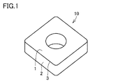
- FIG. 1 is a perspective view illustrating one mode of a cutting tool.
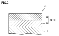
- FIG. 2 is a schematic cross-sectional view of a cutting tool in one aspect of the present embodiment.
- FIG. 3 is a schematic cross-sectional view of a cutting tool in another aspect of this embodiment.
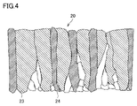
- FIG. 4 is a schematic cross-sectional view for explaining the crystal structure of the hard layer according to this embodiment.
- FIG. 5 is an example of a spectral diagram obtained when the hard layer according to this embodiment is subjected to X-ray diffraction analysis.
- FIG. 6 is a schematic cross-sectional view of a cutting tool in another aspect of this embodiment.
- the surface-coated cutting tool described in Patent Literature 1 is expected to have a hard coating layer configured as described above, thereby improving wear resistance and thereby extending the life of the cutting tool.
- the surface-coated cutting tool described in Patent Document 2 it is expected that delamination and crack propagation are suppressed by having the coating having the above structure, and thus the life of the cutting tool is extended.
- the speed and efficiency of cutting have increased, and the load applied to the cutting tool has increased, resulting in a tendency to shorten the life of the cutting tool. For this reason, it is required to further improve the mechanical properties (for example, wear resistance, chipping resistance, heat resistance, etc.) of coatings of cutting tools.
- the present disclosure has been made in view of the above circumstances, and aims to provide a cutting tool with excellent fracture resistance.
- the cutting tool according to the present disclosure is A cutting tool comprising a substrate and a hard layer provided on the substrate,
- the hard layer includes a first unit layer and a second unit layer, In the hard layer, one or more layers of the first unit layer and the second unit layer are alternately laminated,
- the first unit layer has a thickness of 2 nm or more and 100 nm or less
- the second unit layer has a thickness of 2 nm or more and 100 nm or less
- the first unit layer is made of a compound represented by TiaAlbBcN
- the second unit layer is made of a compound represented by Ti d Ale B f N
- the atomic ratio a of the titanium element in the TiaAlbBcN is 0.25 or more and less than 0.45
- the atomic ratio b of the aluminum element in the TiaAlbBcN is 0.55 or more and less than 0.75
- the hard layer of the cutting tool becomes a cutting tool with excellent chipping resistance. That is, the cutting tool can have excellent chipping resistance by having the configuration as described above. Further, the hard layer provides a cutting tool with excellent heat resistance by setting the atomic ratio of the aluminum element in each of the first unit layer and the second unit layer within the ranges described above.
- fracture resistance means resistance to chipping of a cutting tool during cutting.
- Heat resistance means resistance to abrasion, deformation, etc. of a cutting tool in a high temperature environment.
- the ratio I (200) /I (002) of the intensity I (200) of the X-ray diffraction peak of the (200) plane to the intensity I (002) of the X-ray diffraction peak of the (002) plane in the hard layer is greater than or equal to 2, and
- the half width of the X-ray diffraction peak of the (002) plane is preferably 2 degrees or more.
- the hardness H of the hard layer at room temperature is preferably 30 GPa or more.
- the cutting tool can have excellent wear resistance in addition to excellent chipping resistance.
- wear resistance means resistance to wear of a cutting tool during cutting.
- the ratio H/E of the hardness H of the hard layer to the Young's modulus E of the hard layer at room temperature is preferably 0.07 or more.
- the hard layer preferably has a thickness of 1 ⁇ m or more and 20 ⁇ m or less.
- this embodiment An embodiment of the present disclosure (hereinafter referred to as "this embodiment") will be described below. However, this embodiment is not limited to this.
- the notation of the form "A to Z” means the upper and lower limits of the range (that is, from A to Z), and if no unit is described at A and only a unit is described at Z, then A and the unit of Z are the same.
- the chemical formula when a compound is represented by a chemical formula in which the composition ratio of constituent elements is not limited, such as "TiN”, the chemical formula can be any conventionally known composition ratio (element ratio) shall include At this time, the above chemical formula includes not only stoichiometric compositions but also non-stoichiometric compositions.
- the chemical formula of “TiN” includes not only the stoichiometric composition “Ti 1 N 1 ” but also non-stoichiometric compositions such as “Ti 1 N 0.8 ”. This also applies to the description of compounds other than "TiN".
- a cutting tool comprising a substrate and a hard layer provided on the substrate,
- the hard layer includes a first unit layer and a second unit layer, In the hard layer, one or more layers of the first unit layer and the second unit layer are alternately laminated,
- the first unit layer has a thickness of 2 nm or more and 100 nm or less
- the second unit layer has a thickness of 2 nm or more and 100 nm or less
- the first unit layer is made of a compound represented by TiaAlbBcN
- the second unit layer is made of a compound represented by Ti d Ale B f N
- the atomic ratio a of the titanium element in the TiaAlbBcN is 0.25 or more and less than 0.45
- the atomic ratio b of the aluminum element in the TiaAlbBcN is 0.55 or more and less than 0.75
- the atomic ratio c of the boron element in the TiaAlbBcN is more than 0 and 0.1 or less, the sum of the atomic ratio a,
- cutting tools examples include drills, end mills, indexable cutting inserts for drills, indexable cutting inserts for end mills, indexable cutting inserts for milling, indexable cutting inserts for turning, and metal saws. , gear cutting tools, reamers, taps, and the like.
- FIG. 1 is a perspective view illustrating one aspect of a cutting tool.
- a cutting tool having such a shape is used, for example, as an indexable cutting tip.
- the cutting tool 10 has a rake face 1, a flank face 2, and a cutting edge ridge 3 where the rake face 1 and the flank face 2 intersect. That is, the rake face 1 and the flank face 2 are surfaces connected with the cutting edge ridge 3 interposed therebetween.
- the cutting edge ridge 3 constitutes the cutting edge of the cutting tool 10 .
- Such a shape of the cutting tool 10 can also be grasped as the shape of the base material of the cutting tool. That is, the substrate has a rake face, a flank face, and a cutting edge ridge connecting the rake face and the flank face.
- the base material is a cemented carbide (for example, a tungsten carbide (WC)-based cemented carbide, a cemented carbide containing Co in addition to WC, a carbonitride such as Cr, Ti, Ta, Nb in addition to WC).
- a cemented carbide for example, a tungsten carbide (WC)-based cemented carbide, a cemented carbide containing Co in addition to WC, a carbonitride such as Cr, Ti, Ta, Nb in addition to WC.
- cemented carbide, etc. cermet (mainly composed of TiC, TiN, TiCN, etc.), high-speed steel, ceramics (titanium carbide, silicon carbide, silicon nitride, aluminum nitride, aluminum oxide, etc.), cubic It is preferable to include one selected from the group consisting of type boron nitride sintered bodies (cBN sintered bodies) and diamond sintered bodies.
- cemented carbide especially WC-based cemented carbide
- cermet especially TiCN-based cermet
- the effect of the present embodiment is exhibited even if such a cemented carbide contains free carbon or an abnormal phase called ⁇ phase in the structure.
- the base material used in this embodiment may have a modified surface.
- a ⁇ -free layer may be formed on the surface, or in the case of a cBN sintered body, a surface-hardened layer may be formed. Even if the surface is modified in this way, The effect of this embodiment is shown.
- the substrate may or may not have a chip breaker. included.
- the shape of the ridge line of the cutting edge is sharp edge (the ridge where the rake face and the flank face intersect), honing (sharp edge rounded shape), negative land (chamfered shape), and a combination of honing and negative land. any shape is included.
- the coating according to this embodiment is provided on the substrate.
- the “coating” has the effect of improving various properties such as heat resistance, chipping resistance, and wear resistance of the cutting tool by covering at least part of the base material (for example, part of the rake face). It is.
- the coating preferably covers the entire surface of the substrate. However, it does not depart from the scope of the present embodiment even if a part of the substrate is not covered with the coating or the composition of the coating is partially different.
- the coating includes a hard layer having a first unit layer and a second unit layer.
- the thickness of the coating is preferably 1 ⁇ m or more and 20 ⁇ m or less, more preferably 1.5 ⁇ m or more and 12 ⁇ m or less, and even more preferably 2 ⁇ m or more and 8 ⁇ m or less.
- the thickness of the coating means the total thickness of each layer constituting the coating. Examples of the "layers constituting the coating" include other layers such as the hard layer described above, a base layer described later, an intermediate layer and a surface layer.
- the thickness of the coating is, for example, using a transmission electron microscope (TEM), measuring arbitrary 10 points in a cross-sectional sample parallel to the normal direction of the surface of the base material, the thickness of the measured 10 points can be obtained by taking the average value of The measurement magnification at this time is, for example, 10000 times.
- TEM transmission electron microscope
- the cross-sectional sample include a sample obtained by slicing the cross-section of the cutting tool with an ion slicer. The same is true when measuring the thickness of each of the hard layer, the base layer, the intermediate layer, the surface layer, and the like.
- Examples of transmission electron microscopes include JEM-2100F (trade name) manufactured by JEOL Ltd.
- the hard layer 20 includes a first unit layer 21 and a second unit layer 22 (FIG. 2).
- the hard layer may start from the first unit layer 21 or may start from the second unit layer.
- the hard layer 20 may be provided directly above the base material 11 (FIGS. 2 and 3), as long as the effect of the cutting tool according to the present embodiment is maintained. It may be provided on the substrate 11 via a layer (FIG. 6).
- the hard layer 20 may be provided with another layer such as a surface layer 32 thereon as long as the effect of the cutting tool is maintained (FIG. 6). Further, the hard layer 20 may be provided on the surface of the coating 40 .
- a plurality of hard layers may be provided as long as the effects of the cutting tool are maintained.
- the coating when the coating includes a first hard layer and a second hard layer, the coating further includes an intermediate layer provided between the first hard layer and the second hard layer.
- the hard layer preferably covers the flank face of the base material.
- the hard layer preferably covers the rake face of the substrate. More preferably, the hard layer covers the entire surface of the substrate. However, even if a part of the substrate is not covered with the hard layer, it does not depart from the scope of the present embodiment.
- the thickness of the hard layer is preferably 1 ⁇ m or more and 20 ⁇ m or less, more preferably 1.5 ⁇ m or more and 12 ⁇ m or less, and even more preferably 2 ⁇ m or more and 8 ⁇ m or less.
- the thickness can be measured, for example, by observing the cross section of the cutting tool as described above at a magnification of 10,000 using a transmission electron microscope.
- the ratio I (200) /I (002) of the intensity I (200) of the X-ray diffraction peak of the (200) plane to the intensity I (002) of the X-ray diffraction peak of the (002) plane in the hard layer is 2 or more. and The half width of the X-ray diffraction peak of the (002) plane is preferably 2 degrees or more.
- the “intensity I (200) of the X-ray diffraction peak of the (200) plane” is the diffraction intensity (peak height) at the highest peak among the X-ray diffraction peaks derived from the (200) plane. means. The same applies to the "intensity I (002) of the X-ray diffraction peak of the (002) plane".
- X-ray diffraction measurement by the ⁇ /2 ⁇ method is performed on each of three arbitrary points in the hard layer under the conditions described in the examples described later, and the X-ray of a predetermined crystal plane is measured.
- the diffraction intensity is obtained, and the average value of the obtained three X-ray diffraction intensities is taken as the X-ray diffraction intensity of the predetermined crystal plane.
- line diffraction intensity corresponds to line diffraction intensity (see, for example, FIG. 5).
- the vertical axis indicates the X-ray diffraction intensity
- the horizontal axis indicates the value of 2 ⁇ .
- Examples of the apparatus used for the X-ray diffraction measurement include "SmartLab” (trade name) manufactured by Rigaku Corporation and "X'pert” (trade name) manufactured by PANalytical.
- the X-ray diffraction intensity of the (200) plane is derived from the cubic crystals in the hard layer.
- the intensity I (002) of the X-ray diffraction peak of the (002) plane originates from the hexagonal crystals in the hard layer. Therefore, it is possible to determine whether the hard layer has cubic crystals or hexagonal crystals based on the presence or absence of these peaks.
- the fact that the ratio I (200) /I (002) is 2 or more means that a mixed crystal of the cubic columnar crystals 23 and the hexagonal columnar crystals 24 is formed in the hard layer. (Fig. 4). In each of the cubic columnar crystals 23 and the hexagonal columnar crystals 24, first unit layers and second unit layers are alternately laminated. We omit the structure of
- the upper limit of the above ratio I (200) /I (002) may be, for example, 10 or less, less than 10, or 5 or less.
- the upper limit of the half width of the X-ray diffraction peak of the (002) plane may be 4 degrees or less, or may be 3 degrees or less.
- the hardness H of the hard layer at room temperature is preferably 30 GPa or more, more preferably 30 GPa or more and 50 GPa or less, and even more preferably 35 GPa or more and 45 GPa or less.
- the Young's modulus E of the hard layer at room temperature is preferably 700 GPa or less, more preferably 400 GPa or more and 700 GPa or less, and even more preferably 400 GPa or more and 550 GPa or less.
- the ratio H/E of the hardness H of the hard layer to the Young's modulus E of the hard layer at room temperature is preferably 0.07 or more, more preferably 0.07 or more and 0.12 or less, It is more preferably 0.08 or more and 0.11 or less.
- the hardness H and the Young's modulus E can be obtained by a nanoindentation method according to the standard procedure stipulated in "ISO 14577-1: 2015 Metallic materials-Instrumented indentation test for hardness and materials parameters-". .
- Room temperature as used in this embodiment means 25 degreeC.
- the indentation depth of the indenter should not exceed 1/10 of the thickness of the hard layer in the indentation direction of the indenter.
- the indentation load of the indenter is 1 g.
- the above-described cross-sectional sample may be used as long as the cross-sectional area of the hard layer can be secured to be 10 times wider than the area of the indenter.
- a sample having a cross section inclined with respect to the normal direction of the surface of the base material may be used so that the cross section of the hard layer is sufficiently wide with respect to the indenter.
- Such measurements are performed for at least 10 cross-sectional samples, and the average values of the hardness and Young's modulus obtained for each sample are taken as the hardness H and Young's modulus E of the hard layer. Data that seem to be abnormal values at first glance shall be excluded.
- An example of an apparatus for performing the nanoindentation method is ENT-1100a manufactured by Elionix.
- the thickness of the first unit layer is 2 nm or more and 100 nm or less, preferably 2 nm or more and 50 nm or less, and more preferably 2 nm or more and 10 nm or less.
- the thickness of the first unit layer and the thickness of the second unit layer described later are determined by analysis using electron energy loss spectroscopy (EELS). Specifically, first, in a scanning transmission electron microscope image (STEM image) of the cross-sectional sample described above, an intensity profile corresponding to Al is measured along a direction parallel to the stacking direction of the hard layers.
- STEM image scanning transmission electron microscope image
- the intensity profile is represented as a line graph in which the X axis (horizontal axis) is the distance from the measurement start point on the hard layer and the Y axis (vertical axis) is the intensity (brightness caused by atoms). be done.
- the distance between the point showing the maximum value of the line graph corresponding to Al and the point showing the next maximum value is obtained.
- the obtained distance means the total thickness of the thickness of the first unit layer and the thickness of the second unit layer. Calculate the total thickness obtained in this manner at at least four locations, obtain the average value, and divide the obtained average value by 2 to obtain the thickness of each of the first unit layer and the second unit layer. do.
- the first unit layer is made of a compound represented by TiaAlbBcN .
- Consisting of a compound represented by TiaAlbBcN refers to an embodiment composed only of a compound represented by TiaAlbBcN and an embodiment composed only of a compound represented by TiaAlbBcN . It is a concept that includes aspects consisting of compounds and unavoidable impurities. Examples of unavoidable impurities include carbon (C) and oxygen (O).
- the composition of the first unit layer can be obtained by elemental analysis of the entire first unit layer by energy dispersive X-ray spectroscopy (TEM-EDX) attached to the above cross-sectional sample with a TEM. . The observation magnification at this time is, for example, 20000 times.
- TEM-EDX energy dispersive X-ray spectroscopy
- the atomic ratio a of the titanium element in the above TiaAlbBcN is 0.25 or more and less than 0.45, preferably 0.25 or more and 0.40 or less, and 0.25 or more and 0.35 or less. is more preferable.
- the first unit layer has an appropriate hardness.
- the atomic ratio b of the aluminum element in the above TiaAlbBcN is 0.55 or more and less than 0.75, preferably 0.60 or more and less than 0.75, and 0.65 or more and less than 0.75 is more preferable.
- the first unit layer has excellent heat resistance.
- the atomic ratio c of the boron element in the above TiaAlbBcN is more than 0 and 0.1 or less, preferably 0.01 or more and 0.09 or less, and 0.02 or more and 0.08 or less is more preferable.
- the first unit layer can have an appropriate hardness.
- the sum of the atomic ratio a, the atomic ratio b, and the atomic ratio c is one.
- the thickness of the second unit layer is 2 nm or more and 100 nm or less, preferably 2 nm or more and 50 nm or less, and more preferably 2 nm or more and 10 nm or less.
- the second unit layer is made of a compound represented by TidAleBfN .
- Consisting of a compound represented by Ti d Ale BfN means an embodiment composed only of a compound represented by Ti d Ale BfN and a mode composed only of a compound represented by Ti d Ale BfN It is a concept that includes aspects consisting of compounds and unavoidable impurities. Examples of unavoidable impurities include carbon (C) and oxygen (O).
- the composition of the second unit layer can be obtained by elemental analysis of the entire second unit layer by energy dispersive X-ray spectroscopy (TEM-EDX) attached to the above cross-sectional sample with a TEM. . The observation magnification at this time is, for example, 20000 times.
- the atomic ratio d of the titanium element in the Ti d Ale B f N is 0.35 or more and less than 0.55, preferably 0.35 or more and 0.50 or less, and 0.35 or more and 0.45 or less. is more preferable.
- the first unit layer has an appropriate hardness.
- the atomic ratio e of the aluminum element in the Ti d Ale Bf N is 0.45 or more and less than 0.65, preferably 0.50 or more and less than 0.65, and 0.55 or more and less than 0.65. is more preferable.
- the first unit layer can have an appropriate hardness.
- the atomic ratio f of the boron element in the Ti d Ale B f N is more than 0 and 0.1 or less, preferably 0.01 or more and 0.09 or less, and 0.02 or more and 0.08 or less is more preferable.
- the first unit layer has an appropriate hardness.
- the sum of the atomic ratio d, the atomic ratio e, and the atomic ratio f is one.
- the atomic ratio a and the atomic ratio d preferably satisfy 0.05 ⁇ da ⁇ 0.2 and 0.1 ⁇ da ⁇ 0.2. By setting da within the above range, a cutting tool having excellent chipping resistance can be obtained.
- the atomic ratio b and the atomic ratio e preferably satisfy 0.05 ⁇ be ⁇ 0.2 and 0.1 ⁇ be ⁇ 0.2. By setting be within the above range, a cutting tool having excellent chipping resistance can be obtained.
- the coating may further include other layers as long as the effects of the present embodiment are not impaired.
- Examples of the other layer include a base layer provided between the substrate and the hard layer and a surface layer provided on the hard layer. Further, there is an intermediate layer provided between the first hard layer and the second hard layer in the case where the coating includes the first hard layer and the second hard layer.
- the underlayer may be, for example, a layer made of a compound represented by AlCrN.
- the surface layer may be, for example, a layer made of a compound represented by TiN.
- the intermediate layer may be, for example, a layer made of a compound represented by TiAlN.
- the composition of the other layer can be obtained by elemental analysis of the entire other layer by energy-dispersive X-ray spectroscopy (TEM-EDX) attached to the above cross-sectional sample with a TEM. The observation magnification at this time is, for example, 20000 times.
- TEM-EDX energy-dispersive X-ray spectroscopy
- the thickness of the other layer is not particularly limited as long as it does not impair the effects of the present embodiment.
- the thickness can be measured, for example, by observing the cross section of the cutting tool as described above at a magnification of 10,000 using a transmission electron microscope.
- the method for manufacturing a cutting tool includes: A step of preparing the base material (hereinafter sometimes referred to as "first step”); A step of alternately laminating one or more first unit layers and one or more second unit layers on the base material using a physical vapor deposition method to form the hard layer (hereinafter referred to as the "second step” There is a case.) and, including.
- Physical vapor deposition is a vapor deposition method in which a raw material (also called “evaporation source” or “target”) is vaporized using physical action, and the vaporized raw material is deposited on a base material or the like.
- a raw material also called “evaporation source” or “target”
- Examples of physical vapor deposition include sputtering and arc ion plating.
- the arc ion plating method is preferably used as the physical vapor deposition method used in this embodiment.
- a base material is installed in the device and a target is installed as a cathode, and then a high current is applied to this target to generate an arc discharge.
- the atoms forming the target are vaporized and ionized, and deposited on the substrate to which a negative bias voltage is applied to form a film.
- a substrate is prepared in the first step.
- a cemented carbide base material or a cubic boron nitride sintered body is prepared as the base material.
- the cemented carbide base material and the cubic boron nitride sintered body may be commercially available base materials or may be produced by a general powder metallurgy method.
- a cemented carbide is produced by a general powder metallurgy method, first, a mixed powder is obtained by mixing WC powder and Co powder with a ball mill or the like. After drying the mixed powder, it is molded into a predetermined shape to obtain a molded body.
- a WC—Co-based cemented carbide sintered body
- a predetermined cutting edge processing such as honing treatment to produce a base material made of a WC—Co based cemented carbide.
- any substrate other than those described above can be prepared as long as it is conventionally known as this type of substrate.
- the second step one or more first unit layers and one or more second unit layers are alternately laminated on the substrate by physical vapor deposition to form the hard layer.
- various methods are used depending on the composition of the hard layer to be formed.
- a method of using alloy targets with different grain sizes such as titanium (Ti), aluminum (Al), and boron (B)
- a method of using a plurality of targets with different compositions include a method of using a pulse voltage as the bias voltage, a method of changing the gas flow rate during film formation, and a method of adjusting the rotation speed of a substrate holder that holds the substrate in the film forming apparatus.
- the second step can be performed as follows. First, a chip having an arbitrary shape is mounted as a substrate in the chamber of the film forming apparatus. For example, the substrate is attached to the outer surface of a substrate holder on a rotary table that is rotatably mounted centrally within the chamber of the deposition apparatus. Next, the evaporation source for forming the first unit layer and the evaporation source for forming the second unit layer are arranged to face each other so as to sandwich the substrate holder. A bias power supply is attached to the substrate holder. An arc power source is attached to each of the evaporation source for forming the first unit layer and the evaporation source for forming the second unit layer.
- Nitrogen gas or the like is introduced as a reaction gas while the substrate is rotated in the center of the chamber. Furthermore, the temperature of the substrate is maintained at 400 to 800° C., the reaction gas pressure is maintained at 1 to 10 Pa (partial pressure of nitrogen gas is 5 to 10 Pa), and the voltage of the bias power supply is gradually increased in the range of 30 to 200 V (DC power supply). , an arc current of 80 to 200 A is alternately supplied to the evaporation source for forming the first unit layer and the evaporation source for forming the second unit layer.
- metal ions are generated from the evaporation source for forming the first unit layer and the evaporation source for forming the second unit layer, and when the substrate faces the evaporation source for forming the first unit layer, the second One unit layer is formed, and a second unit layer is formed when the substrate faces the evaporation source for forming the second unit layer.
- the film while changing the voltage of the bias power supply as described above, it is possible to achieve both high hardness of the hard layer and cutting edge quality. After a predetermined time has passed, the supply of the arc current is stopped to form a hard layer (first unit layer and second unit layer) on the surface of the substrate.
- the thickness of each of the first unit layer and the second unit layer is adjusted by adjusting the rotational speed of the substrate. Also, by adjusting the film formation time, the thickness of the hard layer is adjusted to fall within a predetermined range.
- a hard layer may be formed on the surface of the base material other than the part involved in cutting. .
- TiAlN layer a layer made of a compound represented by TiAlN (TiAlN layer) is predominantly cubic and has excellent hardness.
- TiAlN layer a compound represented by TiAlN
- boron is added as a raw material when forming the TiAlN layer, hexagonal crystals are likely to be formed and the hardness decreases. Therefore, there was no concept of using boron in addition to titanium and aluminum as raw materials when forming a TiAlN layer.
- the present inventors added a trace amount of boron in addition to titanium and aluminum as raw materials, and further formed a hard layer so as to have a multilayer structure of the first unit layer and the second unit layer. As a result, it was found for the first time that a cutting tool having unexpectedly excellent heat resistance and excellent chipping resistance could be obtained.
- the substrate is maintained at a temperature of 500-600° C.
- the reaction gas pressure is maintained at 5-10 Pa (the partial pressure of nitrogen gas is 5-8 Pa)
- the voltage of the bias power supply is 30-200 V (DC)
- the raw material of the first unit layer contains titanium, aluminum, and boron, and examples thereof include titanium boride, aluminum metal, and titanium aluminum boride.
- the blending composition of the raw materials of the first unit layer can be appropriately adjusted according to the desired composition of the first unit layer.
- the raw material of the first unit layer may be in the form of a powder or a plate.
- the raw material of the second unit layer contains titanium, aluminum, and boron. Examples thereof include metallic titanium, aluminum boride, and titanium aluminum boride.
- the blending composition of the raw materials for the second unit layer can be appropriately adjusted according to the desired composition of the second unit layer. It is preferable that the mixing composition of the raw material of the second unit layer is different from the mixing composition of the raw material of the first unit layer.
- the raw material for the second unit layer may be in the form of a powder or a plate.
- the reaction gas described above is appropriately set according to the composition of the hard layer.
- the reaction gas include a mixed gas of nitrogen gas and argon gas, nitrogen gas, and the like.
- a step of ion bombardment treatment of the surface of the base material in addition to the above-described steps, between the first step and the second step, a step of ion bombardment treatment of the surface of the base material, A step of forming a base layer between them, a step of forming a surface layer on the hard layer, a step of forming an intermediate layer between the first hard layer and the second hard layer, a surface treatment step, etc. may be performed as appropriate.
- the other layers may be formed by conventional methods.
- indexable cutting insert P for milling (equivalent to JIS P30 cemented carbide, SEMT13T3AGSN) and indexable cutting insert K for milling (equivalent to JIS K30)
- a cemented carbide, SEMT13T3AGSN) was prepared (first step).
- ⁇ Ion bombardment treatment> Prior to the preparation of the coating described below, the surface of the base material was subjected to ion bombardment treatment according to the following procedure. First, the substrate was set in an arc ion plating apparatus. Next, ion bombardment treatment was performed under the following conditions. Gas composition: Ar (100%) Gas pressure: 0.5Pa Bias voltage: 600V (DC power supply) Processing time: 60 minutes
- Coatings were produced by forming hard layers (multilayered structures or single layers) shown in Tables 2-1 to 2-3 on the surfaces of the substrates subjected to the ion bombardment treatment. A method for producing the hard layer will be described below.
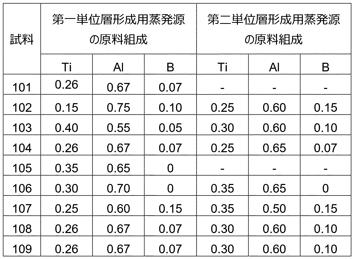
- the evaporation source for forming the first unit layer and the evaporation source for forming the second unit layer used raw material compositions shown in Tables 1-1 and 1-2, respectively.
- the hard layer comprises the first unit layer and the second unit layer having the compositions shown in Tables 2-1 to 2-3, and the base material so as to have the thickness shown in Tables 2-1 to 2-3. It was produced by alternately laminating each layer one by one while adjusting the rotation speed of .
- composition of the hard layer in Tables 2-1 to 2-3 is obtained by elemental analysis of the entire hard layer by energy dispersive X-ray spectroscopy (TEM-EDX) attached to the cross-sectional sample of the TEM as described above. sought by The observation magnification at this time was 20000 times.
- TEM-EDX energy dispersive X-ray spectroscopy
- samples 101 and 105 films were formed using only the evaporation source for forming the first unit layer (Tables 1-2 and 2-3). Therefore, the hard layer in samples 101 and 105 is a single layer rather than a multi-layer structure.
- ⁇ Measurement of thickness of coating (thickness of hard layer)>
- the thickness of the coating (that is, the thickness of the hard layer) is measured using a transmission electron microscope (TEM) (manufactured by JEOL Ltd., trade name: JEM-2100F), parallel to the normal direction of the surface of the substrate. It was obtained by measuring arbitrary 10 points in a cross-sectional sample and averaging the thickness of the measured 10 points. The results are shown in Tables 2-1 and 2-2.
- the thickness of each of the first unit layer and the second unit layer was obtained by analysis using EELS. Specifically, in the STEM image obtained by the above measurement, the intensity profile corresponding to Al was measured along the direction parallel to the stacking direction of the hard layers.
- the intensity profile is represented as a line graph in which the X-axis (horizontal axis) is the distance from the measurement start point on the hard layer and the Y-axis (vertical axis) is the intensity (brightness caused by atoms). In the obtained graph, the distance between the point showing the maximum value of the line graph corresponding to Al and the point showing the next maximum value was determined.
- the obtained distance means the total thickness of the thickness of the first unit layer and the thickness of the second unit layer. Calculate the total thickness obtained in this manner at at least four locations, obtain the average value, and divide the obtained average value by 2 to obtain the thickness of each of the first unit layer and the second unit layer. did. The results are shown in Tables 2-1 and 2-2.
- ⁇ X-ray diffraction analysis of hard layer The hard layer was analyzed by the X-ray diffraction analysis method (XDR analysis method) to obtain the X-ray diffraction intensities I (200) and I (002) of the (200) plane and (002) plane, respectively.
- the conditions for X-ray diffraction analysis are shown below. Tables 3-1 and 3-2 show the obtained I (200) /I (002) and the peak half width of I (002) .
- ENT-1100a (trade name) manufactured by Elionix Co., Ltd. was used as a measuring device. The above measurements were performed on 10 cross-sectional samples, and the average values of the hardness and Young's modulus obtained for each sample were taken as the hardness H and Young's modulus E of the hard layer. Data that appear to be outliers were excluded. A ratio H/E of the hardness H to the Young's modulus E was also obtained. The results are shown in Tables 3-1 and 3-2.
Landscapes
- Chemical & Material Sciences (AREA)
- Engineering & Computer Science (AREA)
- Materials Engineering (AREA)
- Organic Chemistry (AREA)
- Mechanical Engineering (AREA)
- Chemical Kinetics & Catalysis (AREA)
- Metallurgy (AREA)
- Ceramic Engineering (AREA)
- Structural Engineering (AREA)
- Inorganic Chemistry (AREA)
- Cutting Tools, Boring Holders, And Turrets (AREA)
- Physical Vapour Deposition (AREA)
Abstract
Description
基材と、上記基材上に設けられている硬質層と、を備える切削工具であって、
上記硬質層は、第一単位層と第二単位層とを含み、
上記硬質層は、上記第一単位層と上記第二単位層とが交互にそれぞれ一層以上積層されており、
上記第一単位層の厚さは、2nm以上100nm以下であり、
上記第二単位層の厚さは、2nm以上100nm以下であり、
上記第一単位層は、TiaAlbBcNで表される化合物からなり、
上記第二単位層は、TidAleBfNで表される化合物からなり、
上記TiaAlbBcNにおけるチタン元素の原子比aは、0.25以上0.45未満であり、
上記TiaAlbBcNにおけるアルミニウム元素の原子比bは、0.55以上0.75未満であり、
上記TiaAlbBcNにおけるホウ素元素の原子比cは、0を超えて0.1以下であり、
上記原子比a、上記原子比b及び上記原子比cの合計は、1であり、
上記TidAleBfNにおけるチタン元素の原子比dは、0.35以上0.55未満であり、
上記TidAleBfNにおけるアルミニウム元素の原子比eは、0.45以上0.65未満であり、
上記TidAleBfNにおけるホウ素元素の原子比fは、0を超えて0.1以下であり、
上記原子比d、上記原子比e及び上記原子比fの合計は、1であり、
上記原子比a及び上記原子比dは、0.05≦d-a≦0.2を満たし、
上記原子比b及び上記原子比eは、0.05≦b-e≦0.2を満たす。
特許文献1に記載の表面被覆切削工具では、上記のような構成の硬質被覆層を有することにより、耐摩耗性が向上し、以って切削工具の寿命が長くなることが期待されている。特許文献2に記載の表面被覆切削工具では、上記のような構成の被膜を有することにより、層間剥離及び亀裂伝播が抑制され、以って切削工具の寿命が長くなることが期待されている。しかしながら、近年の切削加工においては、高速化及び高能率化が進行し、切削工具にかかる負荷が増大し、切削工具の寿命が短期化する傾向があった。このため、切削工具の被膜の機械特性(例えば、耐摩耗性、耐欠損性、耐熱性等)を更に向上させることが求められている。
上記によれば、耐欠損性に優れる切削工具を提供することが可能になる。
最初に本開示の実施態様を列記して説明する。
[1]本開示に係る切削工具は、
基材と、上記基材上に設けられている硬質層と、を備える切削工具であって、
上記硬質層は、第一単位層と第二単位層とを含み、
上記硬質層は、上記第一単位層と上記第二単位層とが交互にそれぞれ一層以上積層されており、
上記第一単位層の厚さは、2nm以上100nm以下であり、
上記第二単位層の厚さは、2nm以上100nm以下であり、
上記第一単位層は、TiaAlbBcNで表される化合物からなり、
上記第二単位層は、TidAleBfNで表される化合物からなり、
上記TiaAlbBcNにおけるチタン元素の原子比aは、0.25以上0.45未満であり、
上記TiaAlbBcNにおけるアルミニウム元素の原子比bは、0.55以上0.75未満であり、
上記TiaAlbBcNにおけるホウ素元素の原子比cは、0を超えて0.1以下であり、
上記原子比a、上記原子比b及び上記原子比cの合計は、1であり、
上記TidAleBfNにおけるチタン元素の原子比dは、0.35以上0.55未満であり、
上記TidAleBfNにおけるアルミニウム元素の原子比eは、0.45以上0.65未満であり、
上記TidAleBfNにおけるホウ素元素の原子比fは、0を超えて0.1以下であり、
上記原子比d、上記原子比e及び上記原子比fの合計は、1であり、
上記原子比a及び上記原子比dは、0.05≦d-a≦0.2を満たし、
上記原子比b及び上記原子比eは、0.05≦b-e≦0.2を満たす。
上記(002)面のX線回折ピークの半価幅が2度以上であることが好ましい。このように規定することで、上記切削工具は更に優れた耐欠損性を有することが可能になる。また、上記切削工具は更に優れた耐熱性を有することが可能になる。
以下、本開示の一実施形態(以下「本実施形態」と記す。)について説明する。ただし、本実施形態はこれに限定されるものではない。本明細書において「A~Z」という形式の表記は、範囲の上限下限(すなわちA以上Z以下)を意味し、Aにおいて単位の記載がなく、Zにおいてのみ単位が記載されている場合、Aの単位とZの単位とは同じである。さらに、本明細書において、例えば「TiN」等のように、構成元素の組成比が限定されていない化学式によって化合物が表された場合には、その化学式は従来公知のあらゆる組成比(元素比)を含むものとする。このとき上記化学式は、化学量論組成のみならず、非化学量論組成も含むものとする。例えば「TiN」の化学式には、化学量論組成「Ti1N1」のみならず、例えば「Ti1N0.8」のような非化学量論組成も含まれる。このことは、「TiN」以外の化合物の記載についても同様である。
基材と、上記基材上に設けられている硬質層と、を備える切削工具であって、
上記硬質層は、第一単位層と第二単位層とを含み、
上記硬質層は、上記第一単位層と上記第二単位層とが交互にそれぞれ一層以上積層されており、
上記第一単位層の厚さは、2nm以上100nm以下であり、
上記第二単位層の厚さは、2nm以上100nm以下であり、
上記第一単位層は、TiaAlbBcNで表される化合物からなり、
上記第二単位層は、TidAleBfNで表される化合物からなり、
上記TiaAlbBcNにおけるチタン元素の原子比aは、0.25以上0.45未満であり、
上記TiaAlbBcNにおけるアルミニウム元素の原子比bは、0.55以上0.75未満であり、
上記TiaAlbBcNにおけるホウ素元素の原子比cは、0を超えて0.1以下であり、
上記原子比a、上記原子比b及び上記原子比cの合計は、1であり、
上記TidAleBfNにおけるチタン元素の原子比dは、0.35以上0.55未満であり、
上記TidAleBfNにおけるアルミニウム元素の原子比eは、0.45以上0.65未満であり、
上記TidAleBfNにおけるホウ素元素の原子比fは、0を超えて0.1以下であり、
上記原子比d、上記原子比e及び上記原子比fの合計は、1であり、
上記原子比a及び上記原子比dは、0.05≦d-a≦0.2を満たし、
上記原子比b及び上記原子比eは、0.05≦b-e≦0.2を満たす。
本実施形態の基材は、この種の基材として従来公知のものであればいずれのものも使用することができる。例えば、上記基材は、超硬合金(例えば、炭化タングステン(WC)基超硬合金、WCの他にCoを含む超硬合金、WCの他にCr、Ti、Ta、Nb等の炭窒化物を添加した超硬合金等)、サーメット(TiC、TiN、TiCN等を主成分とするもの)、高速度鋼、セラミックス(炭化チタン、炭化珪素、窒化珪素、窒化アルミニウム、酸化アルミニウム等)、立方晶型窒化硼素焼結体(cBN焼結体)及びダイヤモンド焼結体からなる群から選ばれる1種を含むことが好ましい。
本実施形態に係る被膜は、上記基材上に設けられている。「被膜」は、上記基材の少なくとも一部(例えば、すくい面の一部)を被覆することで、切削工具における耐熱性、耐欠損性、耐摩耗性等の諸特性を向上させる作用を有するものである。上記被膜は、上記基材の全面を被覆することが好ましい。しかしながら、上記基材の一部が上記被膜で被覆されていなかったり被膜の構成が部分的に異なっていたりしていたとしても本実施形態の範囲を逸脱するものではない。上記被膜は、第一単位層と第二単位層とを有する硬質層を含む。
本実施形態に係る硬質層20は、第一単位層21と、第二単位層22とを含む(図2)。上記硬質層20は、上記第一単位層21と上記第二単位層22とが交互にそれぞれ一層以上積層されている(図2、図3、図6)。上記硬質層は、上記第一単位層21から始まっていてもよいし、上記第二単位層から始まっていてもよい。上記硬質層20は、本実施形態に係る切削工具が奏する効果を維持する限り、上記基材11の直上に設けられていてもよいし(図2、図3)、下地層31等の他の層を介して上記基材11の上に設けられていてもよい(図6)。上記硬質層20は、切削工具が奏する効果を維持する限り、その上に表面層32等の他の層が設けられていてもよい(図6)。また、上記硬質層20は、上記被膜40の表面に設けられていてもよい。
上記硬質層における(002)面のX線回折ピークの強度I(002)に対する(200)面のX線回折ピークの強度I(200)の比I(200)/I(002)が、2以上であり、
上記(002)面のX線回折ピークの半価幅が2度以上であることが好ましい。ここで、「(200)面のX線回折ピークの強度I(200)」とは、(200)面に由来するX線回折ピークのうち、最も高いピークにおける回折強度(ピークの高さ)を意味する。「(002)面のX線回折ピークの強度I(002)」についても同様である。
本実施形態において、室温における上記硬質層の硬度Hは、30GPa以上であることが好ましく、30GPa以上50GPa以下であることがより好ましく、35GPa以上45GPa以下であることが更に好ましい。
上記第一単位層の厚さは、2nm以上100nm以下であり、2nm以上50nm以下であることが好ましく、2nm以上10nm以下であることがより好ましい。上記第一単位層の厚さ及び後述する第二単位層の厚さは、電子エネルギー損失分光法(EELS)を用いた分析によって求められる。具体的には、まず上述の断面サンプルにおける走査透過電子顕微鏡像(STEM像)において、上記硬質層の積層方向に平行な方向に沿ってAlに対応する強度プロファイルを測定する。このとき、上記強度プロファイルは、X軸(横軸)を上記硬質層上の測定開始点からの距離とし、Y軸(縦軸)を強度(原子に起因する明るさ)とした折れ線グラフとして表される。次に得られたグラフにおいて、Alに対応する折れ線グラフの極大値を示す点と、次の極大値を示す点との距離を求める。求められた距離は、第一単位層の厚さと第二単位層の厚さとの合計厚さを意味している。このようにして求められた各合計厚さを少なくとも4カ所算出し、それの平均値を求め、求められた平均値を2で除した値を第一単位層及び第二単位層それぞれの厚さとする。
上記第二単位層の厚さは、2nm以上100nm以下であり、2nm以上50nm以下であることが好ましく、2nm以上10nm以下であることがより好ましい。
本実施形態の効果を損なわない限り、上記被膜は、他の層を更に含んでいてもよい。上記他の層としては、例えば、上記基材と上記硬質層との間に設けられている下地層及び上記硬質層上に設けられている表面層等が挙げられる。また、上記被膜が第一の硬質層と第二の硬質層とを含む場合における上記第一の硬質層と上記第二の硬質層との間に設けられている中間層が挙げられる。
本実施形態に係る切削工具の製造方法は、
上記基材を準備する工程(以下、「第1工程」という場合がある。)と、
物理的蒸着法を用いて、上記基材上に第一単位層と第二単位層とを交互にそれぞれ1層以上積層して、上記硬質層を形成する工程(以下、「第2工程」という場合がある。)と、を含む。
第1工程では基材を準備する。例えば、基材として超硬合金基材、又は立方晶窒化ホウ素焼結体が準備される。超硬合金基材及び立方晶窒化ホウ素焼結体は、市販の基材を用いてもよく、一般的な粉末冶金法で製造してもよい。例えば、一般的な粉末冶金法で超硬合金を製造する場合、まず、ボールミル等によってWC粉末とCo粉末等とを混合して混合粉末を得る。当該混合粉末を乾燥した後、所定の形状に成形して成形体を得る。さらに当該成形体を焼結することにより、WC-Co系超硬合金(焼結体)を得る。次いで当該焼結体に対して、ホーニング処理等の所定の刃先加工を施すことにより、WC-Co系超硬合金からなる基材を製造することができる。第1工程では、上記以外の基材であっても、この種の基材として従来公知のものであればいずれも準備可能である。
第2工程では、物理的蒸着法を用いて、上記基材上に第一単位層と第二単位層とを交互にそれぞれ1層以上積層して、上記硬質層を形成する。その方法としては、形成しようとする硬質層の組成に応じて、各種の方法が用いられる。例えば、チタン(Ti)、アルミニウム(Al)及びホウ素(B)等の粒径をそれぞれ変化させた合金製ターゲットを使用する方法、それぞれ組成の異なる複数のターゲットを使用する方法、成膜時に印可するバイアス電圧をパルス電圧とする方法、成膜時にガス流量を変化させる方法、又は、成膜装置において基材を保持する基材ホルダの回転速度を調整する方法等を挙げることができる。
上記第2工程において、第一単位層の原料は、チタン、アルミニウム、及びホウ素を含み、例えば、ホウ化チタン、金属アルミニウム、ホウ化チタンアルミニウム等が挙げられる。上記第一単位層の原料の配合組成は、目的とする第一単位層の組成に応じて適宜調整が可能である。上記第一単位層の原料は、粉末状であってもよいし、平板状であってもよい。
上記第2工程において、第二単位層の原料は、チタン、アルミニウム、及びホウ素を含例えば、金属チタン、ホウ化アルミニウム、ホウ化チタンアルミニウム等が挙げられる。上記第二単位層の原料の配合組成は、目的とする第二単位層の組成に応じて適宜調整が可能である。上記第二単位層の原料の配合組成は、上記第一単位層の原料の配合組成と異なることが好ましい。上記第二単位層の原料は、粉末状であってもよいし、平板状であってもよい。
本実施形態に係る製造方法では、上述した工程の他にも、第1工程と第2工程との間に、上記基材の表面をイオンボンバードメント処理する工程、基材と上記硬質層との間に下地層を形成する工程、上記硬質層の上に表面層を形成する工程、第一の硬質層と第二の硬質層との間に中間層を形成する工程及び、表面処理する工程等を適宜行ってもよい。
<基材の準備>
まず、被膜を形成させる対象となる基材として、転削加工用刃先交換型切削チップP(JIS規格 P30相当超硬合金、SEMT13T3AGSN)及び転削加工用刃先交換型切削チップK(JIS規格 K30相当超硬合金、SEMT13T3AGSN)を準備した(第1工程)。
後述する被膜の作製に先立って、以下の手順で上記基材の表面にイオンボンバードメント処理を行った。まず、上記基材をアークイオンプレーティング装置にセットした。次に、以下の条件によってイオンボンバードメント処理を行った。
ガス組成 : Ar(100%)
ガス圧 : 0.5Pa
バイアス電圧: 600V(直流電源)
処理時間 : 60分
イオンボンバードメント処理を行った上記基材の表面上に、表2-1~表2-3に示される硬質層(多層構造、又は単層)を形成することによって、被膜を作製した。以下、硬質層の作製方法について説明する。
試料1~22、試料102~104、及び試料106~109においては、基材(転削加工用刃先交換型切削チップP及び転削加工用刃先交換型切削チップK)をチャンバ内の中央で回転させた状態で、反応ガスとして窒素ガスを導入した。さらに、基材を温度550℃に、反応ガス圧を8Pa(窒素ガスの分圧:8Pa)に維持し、バイアス電源の電圧を35~180Vの範囲で徐々に変化させながら第一単位層形成用の蒸発源及び第二単位層形成用の蒸発源にそれぞれ90Aのアーク電流を交互に供給した。これにより、第一単位層形成用の蒸発源及び第二単位層形成用の蒸発源からそれぞれ金属イオンを発生させ、所定の時間が経過したところでアーク電流の供給を止めて、基材の表面上に表2-1~表2-3に示す組成の硬質層を形成した(第2工程)。ここで、第一単位層形成用の蒸発源及び第二単位層形成用の蒸発源は、それぞれ表1-1及び表1-2に示す原料組成のものを用いた。このとき硬質層は、表2-1~表2-3に示す組成を有する第一単位層及び第二単位層を、表2-1~表2-3に示す厚さを有するように基材の回転速度を調整しながら、それぞれ1層ずつ交互に積層することによって作製した。表2-1~表2-3における硬質層の組成は、上述したように断面サンプルをTEMに付帯のエネルギー分散型X線分光法(TEM-EDX)で、硬質層の全体を元素分析することによって求めた。このときの観察倍率は、20000倍であった。



上述のようにして作製した試料1~22及び試料101~109の切削工具を用いて、以下のように、切削工具の各特性を評価した。なお、試料1~22の切削工具は実施例に対応し、試料101~109の切削工具は比較例に対応する。
被膜の厚さ(すなわち、硬質層の厚さ)は、透過型電子顕微鏡(TEM)(日本電子株式会社製、商品名:JEM-2100F)を用いて、基材の表面の法線方向に平行な断面サンプルにおける任意の10点を測定し、測定された10点の厚さの平均値をとることで求めた。結果を表2-1及び表2-2に示す。
第一単位層及び第二単位層それぞれの厚さは、EELSを用いた分析によって求めた。具体的には、上述の測定によって得られたSTEM像において、上記硬質層の積層方向に平行な方向に沿ってAlに対応する強度プロファイルを測定した。上記強度プロファイルは、X軸(横軸)を上記硬質層上の測定開始点からの距離とし、Y軸(縦軸)を強度(原子に起因する明るさ)とした折れ線グラフとして表した。得られたグラフにおいて、Alに対応する折れ線グラフの極大値を示す点と、次の極大値を示す点との距離を求めた。求められた距離は、第一単位層の厚さと第二単位層の厚さとの合計厚さを意味している。このようにして求められた各合計厚さを少なくとも4カ所算出し、それの平均値を求め、求められた平均値を2で除した値を第一単位層及び第二単位層それぞれの厚さとした。結果を表2-1及び表2-2に示す。
硬質層についてX線回折分析法(XDR分析法)による分析を行って、(200)面及び(002)面それぞれのX線回折強度I(200)、及びI(002)を求めた。X線回折分析の条件を以下に示す。求められたI(200)/I(002)、及びI(002)のピーク半価幅を表3-1及び表3-2に示す。
X線回折分析の条件
走査軸:2θ-θ
X線源:Cu-Kα線(1.541862Å)
検出器:0次元検出器(シンチレーションカウンタ)
管電圧:45kV
管電流:40mA
入射光学系:ミラーの利用
受光光学系:アナライザ結晶(PW3098/27)の利用
ステップ:0.03°
積算時間:2秒
スキャン範囲(2θ):20°~80°
「ISO 14577-1: 2015 Metallic materials-Instrumented indentation test for hardness and materials parameters-」において定められている標準手順によるナノインデンテーション法によって、各切削工具における硬質層の硬度Hとヤング率Eとを測定した。ここで、圧子の押し込み深さは100nmに設定した。圧子の押し込み荷重は、1gとした。測定温度は、室温(25℃)とした。また、サンプルは、上記硬質層の断面積が上記圧子の面積に対して10倍の広さを確保できるように鏡面加工した断面サンプルを用いた。測定装置は、株式会社エリオニクス製のENT-1100a(商品名)を用いた。上記測定は、10個の断面サンプルについて行い、それぞれのサンプルで求められた硬度及びヤング率の平均値を、当該硬質層の硬度H及びヤング率Eとした。なお、一見して異常値と思われるデータについては、除外した。また、上記ヤング率Eに対する上記硬度Hの比H/Eも求めた。結果を表3-1及び表3-2に示す。


<切削評価(1)>
得られた切削工具(転削加工用刃先交換型切削チップP)を用いて、以下に示す切削条件にて切削加工(切削距離:900mm)を行った。その後、光学顕微鏡を用いて、切削工具の刃先における破損の有無を観察した。同様の切削試験を10回行い、刃先の破損率(%)を算出した。以下の切削条件による切削加工において、切削工具の刃先には衝撃による負荷が繰り返しかかると考えられる。そのため、上記破損率が低い切削工具は、耐欠損性に優れると評価できる。結果を表4-1及び表4-2に示す。
(切削条件)
被削材:S50C(中心距離18mm間隔でΦ8の穴が存在している)
切削速度:160m/min.
送り量:0.65mm/t
切込み(軸方向):2.5mm
切込み(径方向):工具径の100%
乾式
<切削評価(2)>
得られた切削工具(転削加工用刃先交換型切削チップK)を用いて、以下に示す切削条件にて切削加工を行ない、刃先の切り込み境界付近の逃げ面欠損幅が0.5mmになるまでの切削距離を測定した。結果を表4-1及び表4-2に示す。表4-1及び表4-2において、切削距離の長い方がより耐欠損性に優れていることを示している。
(切削条件)
被削材:インコネル718(形状:角材)
切削速度:30m/min.
送り量:0.35mm/t
切込み(軸方向):2mm
切込み(径方向):工具径の70%
湿式
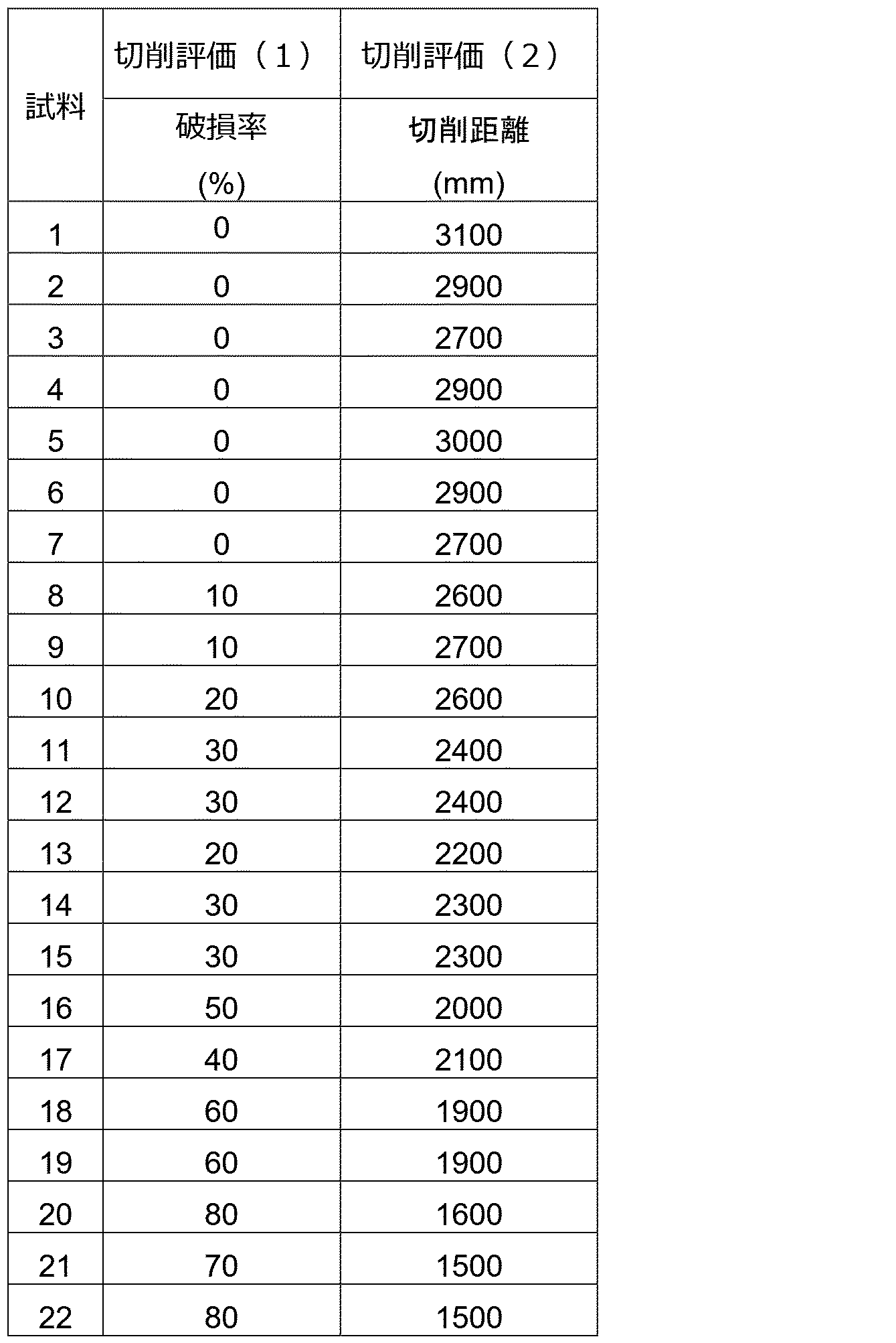

切削評価(1)の結果から、試料1~22の切削工具は、破損率が80%以下であり、良好な結果が得られた。一方、試料101~109の切削工具は、破損率が90%以上であった。以上の結果から、実施例に係る試料1~22の切削工具は、耐欠損性に優れることが分かった(表4-1及び表4-2)。
Claims (5)
- 基材と、前記基材上に設けられている硬質層と、を備える切削工具であって、
前記硬質層は、第一単位層と第二単位層とを含み、
前記硬質層は、前記第一単位層と前記第二単位層とが交互にそれぞれ一層以上積層されており、
前記第一単位層の厚さは、2nm以上100nm以下であり、
前記第二単位層の厚さは、2nm以上100nm以下であり、
前記第一単位層は、TiaAlbBcNで表される化合物からなり、
前記第二単位層は、TidAleBfNで表される化合物からなり、
前記TiaAlbBcNにおけるチタン元素の原子比aは、0.25以上0.45未満であり、
前記TiaAlbBcNにおけるアルミニウム元素の原子比bは、0.55以上0.75未満であり、
前記TiaAlbBcNにおけるホウ素元素の原子比cは、0を超えて0.1以下であり、
前記原子比a、前記原子比b及び前記原子比cの合計は、1であり、
前記TidAleBfNにおけるチタン元素の原子比dは、0.35以上0.55未満であり、
前記TidAleBfNにおけるアルミニウム元素の原子比eは、0.45以上0.65未満であり、
前記TidAleBfNにおけるホウ素元素の原子比fは、0を超えて0.1以下であり、
前記原子比d、前記原子比e及び前記原子比fの合計は、1であり、
前記原子比a及び前記原子比dは、0.05≦d-a≦0.2を満たし、
前記原子比b及び前記原子比eは、0.05≦b-e≦0.2を満たす、切削工具。 - 前記硬質層における(002)面のX線回折ピークの強度I(002)に対する(200)面のX線回折ピークの強度I(200)の比I(200)/I(002)が、2以上であり、
前記(002)面のX線回折ピークの半価幅が2度以上である、請求項1に記載の切削工具。 - 室温における前記硬質層の硬度Hは、30GPa以上である、請求項1又は請求項2に記載の切削工具。
- 室温における前記硬質層のヤング率Eに対する前記硬質層の硬度Hの比H/Eは、0.07以上である、請求項3に記載の切削工具。
- 前記硬質層の厚さは、1μm以上20μm以下である、請求項1から請求項4のいずれか一項に記載の切削工具。
Priority Applications (5)
| Application Number | Priority Date | Filing Date | Title |
|---|---|---|---|
| EP21926497.5A EP4215302B1 (en) | 2021-02-17 | 2021-02-17 | Cutting tool |
| PCT/JP2021/005902 WO2022176057A1 (ja) | 2021-02-17 | 2021-02-17 | 切削工具 |
| JP2021541445A JP7226688B2 (ja) | 2021-02-17 | 2021-02-17 | 切削工具 |
| US18/033,564 US12319996B2 (en) | 2021-02-17 | 2021-02-17 | Cutting tool |
| CN202180071677.2A CN116390824A (zh) | 2021-02-17 | 2021-02-17 | 切削工具 |
Applications Claiming Priority (1)
| Application Number | Priority Date | Filing Date | Title |
|---|---|---|---|
| PCT/JP2021/005902 WO2022176057A1 (ja) | 2021-02-17 | 2021-02-17 | 切削工具 |
Publications (1)
| Publication Number | Publication Date |
|---|---|
| WO2022176057A1 true WO2022176057A1 (ja) | 2022-08-25 |
Family
ID=82930324
Family Applications (1)
| Application Number | Title | Priority Date | Filing Date |
|---|---|---|---|
| PCT/JP2021/005902 Ceased WO2022176057A1 (ja) | 2021-02-17 | 2021-02-17 | 切削工具 |
Country Status (5)
| Country | Link |
|---|---|
| US (1) | US12319996B2 (ja) |
| EP (1) | EP4215302B1 (ja) |
| JP (1) | JP7226688B2 (ja) |
| CN (1) | CN116390824A (ja) |
| WO (1) | WO2022176057A1 (ja) |
Cited By (3)
| Publication number | Priority date | Publication date | Assignee | Title |
|---|---|---|---|---|
| US12059731B1 (en) | 2023-04-28 | 2024-08-13 | Sumitomo Electric Hardmetal Corp. | Cutting tool |
| WO2026018875A1 (ja) * | 2024-07-18 | 2026-01-22 | 京セラ株式会社 | 被覆工具、切削工具、および切削加工物の製造方法 |
| EP4703070A4 (en) * | 2023-04-28 | 2026-04-08 | Sumitomo Electric Hardmetal Corp | CUTTING TOOL |
Families Citing this family (2)
| Publication number | Priority date | Publication date | Assignee | Title |
|---|---|---|---|---|
| EP4578992A1 (en) * | 2023-12-28 | 2025-07-02 | Voestalpine Eifeler Vacotec Gmbh | Workpiece having a hard material layer |
| US20250389013A1 (en) * | 2024-06-20 | 2025-12-25 | Sumitomo Electric Hardmetal Corp. | Cutting tool |
Citations (8)
| Publication number | Priority date | Publication date | Assignee | Title |
|---|---|---|---|---|
| JP2007030130A (ja) * | 2005-07-29 | 2007-02-08 | Mitsubishi Materials Corp | 合金鋼の高速歯切加工で硬質被覆層がすぐれた耐摩耗性を発揮する表面被覆超硬合金製歯切工具 |
| JP2007038378A (ja) * | 2005-08-05 | 2007-02-15 | Mitsubishi Materials Corp | 難削材の高速切削加工で硬質被覆層がすぐれた耐チッピング性を発揮する表面被覆超硬合金製切削工具 |
| JP2011224717A (ja) * | 2010-04-20 | 2011-11-10 | Mitsubishi Materials Corp | 表面被覆切削工具 |
| JP2011224715A (ja) | 2010-04-20 | 2011-11-10 | Mitsubishi Materials Corp | 硬質被覆層がすぐれた耐摩耗性を発揮する表面被覆切削工具 |
| WO2017169498A1 (ja) * | 2016-03-28 | 2017-10-05 | 住友電工ハードメタル株式会社 | 表面被覆切削工具、およびその製造方法 |
| JP2017193004A (ja) | 2016-04-19 | 2017-10-26 | 住友電工ハードメタル株式会社 | 表面被覆切削工具 |
| JP2019005867A (ja) * | 2017-06-26 | 2019-01-17 | 三菱マテリアル株式会社 | 硬質被覆層がすぐれた耐チッピング性を発揮する表面被覆切削工具 |
| WO2019035220A1 (ja) * | 2017-08-15 | 2019-02-21 | 三菱日立ツール株式会社 | 被覆切削工具 |
Family Cites Families (26)
| Publication number | Priority date | Publication date | Assignee | Title |
|---|---|---|---|---|
| JP2793696B2 (ja) * | 1990-05-17 | 1998-09-03 | 神鋼コベルコツール株式会社 | 耐摩耗性皮膜 |
| JP2006116831A (ja) * | 2004-10-22 | 2006-05-11 | Sony Corp | プリンタ及びプリンタの制御方法 |
| JP5234931B2 (ja) * | 2008-06-23 | 2013-07-10 | 株式会社神戸製鋼所 | 硬質皮膜被覆部材および成形用冶工具 |
| JP5730535B2 (ja) * | 2010-10-29 | 2015-06-10 | 株式会社神戸製鋼所 | 硬質皮膜形成部材および硬質皮膜の形成方法 |
| US8409702B2 (en) * | 2011-02-07 | 2013-04-02 | Kennametal Inc. | Cubic aluminum titanium nitride coating and method of making same |
| WO2013002385A1 (ja) * | 2011-06-30 | 2013-01-03 | 京セラ株式会社 | 表面被覆部材 |
| KR101351845B1 (ko) * | 2012-05-02 | 2014-01-16 | 한국야금 주식회사 | 절삭공구용 경질피막 |
| JP6090063B2 (ja) * | 2012-08-28 | 2017-03-08 | 三菱マテリアル株式会社 | 表面被覆切削工具 |
| US9103036B2 (en) * | 2013-03-15 | 2015-08-11 | Kennametal Inc. | Hard coatings comprising cubic phase forming compositions |
| JP2015066644A (ja) * | 2013-09-30 | 2015-04-13 | 三菱マテリアル株式会社 | 高速切削加工で硬質被覆層がすぐれた耐摩耗性と耐チッピング性を発揮する表面被覆切削工具 |
| JP6417959B2 (ja) * | 2014-01-22 | 2018-11-07 | 三菱マテリアル株式会社 | 硬質被覆層がすぐれた耐チッピング性を発揮する表面被覆切削工具 |
| US9849532B2 (en) * | 2014-06-12 | 2017-12-26 | Kennametal Inc. | Composite wear pad and methods of making the same |
| JP6284034B2 (ja) * | 2014-09-25 | 2018-02-28 | 三菱マテリアル株式会社 | 硬質被覆層がすぐれた耐チッピング性を発揮する表面被覆切削工具 |
| KR20170138444A (ko) * | 2015-04-20 | 2017-12-15 | 쎄코 툴스 에이비 | 코팅된 절삭 공구 및 절삭 공구를 코팅하는 방법 |
| WO2016175166A1 (ja) * | 2015-04-27 | 2016-11-03 | 株式会社タンガロイ | 被覆切削工具 |
| KR101753104B1 (ko) * | 2015-09-18 | 2017-07-05 | 한국야금 주식회사 | 절삭공구용 경질피막 |
| EP3360631B1 (en) * | 2015-10-07 | 2022-11-16 | Tungaloy Corporation | Coated cutting tool |
| US10570501B2 (en) * | 2017-05-31 | 2020-02-25 | Kennametal Inc. | Multilayer nitride hard coatings |
| EP3450591A1 (en) * | 2017-08-30 | 2019-03-06 | Seco Tools Ab | A coated cutting tool and a method for coating the cutting tool |
| WO2019048507A1 (en) * | 2017-09-05 | 2019-03-14 | Oerlikon Surface Solutions Ag, Pfäffikon | ALTIN FILMS RICH IN AL |
| KR102350224B1 (ko) * | 2018-03-22 | 2022-01-14 | 스미또모 덴꼬오 하드메탈 가부시끼가이샤 | 표면 피복 절삭 공구 및 그 제조 방법 |
| US20210046561A1 (en) | 2019-04-19 | 2021-02-18 | Sumitomo Electric Hardmetal Corp. | Cutting tool |
| US12544837B2 (en) * | 2019-06-19 | 2026-02-10 | Ab Sandvik Coromant | Coated cutting tool |
| WO2021085253A1 (ja) * | 2019-10-29 | 2021-05-06 | 三菱マテリアル株式会社 | 表面被覆切削工具 |
| CN111270202B (zh) * | 2020-03-17 | 2022-03-25 | 株洲华锐精密工具股份有限公司 | 一种切削刀具用成分结构双梯度功能涂层及其制备方法 |
| KR102172454B1 (ko) * | 2020-08-24 | 2020-10-30 | 주식회사 와이지-원 | 다층 피복 절삭 소재, 그 제조 방법 및 이를 포함하는 기계가공용 절삭 공구 인서트 |
-
2021
- 2021-02-17 WO PCT/JP2021/005902 patent/WO2022176057A1/ja not_active Ceased
- 2021-02-17 US US18/033,564 patent/US12319996B2/en active Active
- 2021-02-17 CN CN202180071677.2A patent/CN116390824A/zh active Pending
- 2021-02-17 JP JP2021541445A patent/JP7226688B2/ja active Active
- 2021-02-17 EP EP21926497.5A patent/EP4215302B1/en active Active
Patent Citations (8)
| Publication number | Priority date | Publication date | Assignee | Title |
|---|---|---|---|---|
| JP2007030130A (ja) * | 2005-07-29 | 2007-02-08 | Mitsubishi Materials Corp | 合金鋼の高速歯切加工で硬質被覆層がすぐれた耐摩耗性を発揮する表面被覆超硬合金製歯切工具 |
| JP2007038378A (ja) * | 2005-08-05 | 2007-02-15 | Mitsubishi Materials Corp | 難削材の高速切削加工で硬質被覆層がすぐれた耐チッピング性を発揮する表面被覆超硬合金製切削工具 |
| JP2011224717A (ja) * | 2010-04-20 | 2011-11-10 | Mitsubishi Materials Corp | 表面被覆切削工具 |
| JP2011224715A (ja) | 2010-04-20 | 2011-11-10 | Mitsubishi Materials Corp | 硬質被覆層がすぐれた耐摩耗性を発揮する表面被覆切削工具 |
| WO2017169498A1 (ja) * | 2016-03-28 | 2017-10-05 | 住友電工ハードメタル株式会社 | 表面被覆切削工具、およびその製造方法 |
| JP2017193004A (ja) | 2016-04-19 | 2017-10-26 | 住友電工ハードメタル株式会社 | 表面被覆切削工具 |
| JP2019005867A (ja) * | 2017-06-26 | 2019-01-17 | 三菱マテリアル株式会社 | 硬質被覆層がすぐれた耐チッピング性を発揮する表面被覆切削工具 |
| WO2019035220A1 (ja) * | 2017-08-15 | 2019-02-21 | 三菱日立ツール株式会社 | 被覆切削工具 |
Non-Patent Citations (2)
| Title |
|---|
| "Metallic materials - Instrumented indentation test for hardness and materials parameters", ISO 14577-1: 2015 |
| See also references of EP4215302A4 |
Cited By (4)
| Publication number | Priority date | Publication date | Assignee | Title |
|---|---|---|---|---|
| US12059731B1 (en) | 2023-04-28 | 2024-08-13 | Sumitomo Electric Hardmetal Corp. | Cutting tool |
| EP4494788A4 (en) * | 2023-04-28 | 2025-07-23 | Sumitomo Electric Hardmetal Corp | CUTTING TOOL |
| EP4703070A4 (en) * | 2023-04-28 | 2026-04-08 | Sumitomo Electric Hardmetal Corp | CUTTING TOOL |
| WO2026018875A1 (ja) * | 2024-07-18 | 2026-01-22 | 京セラ株式会社 | 被覆工具、切削工具、および切削加工物の製造方法 |
Also Published As
| Publication number | Publication date |
|---|---|
| EP4215302B1 (en) | 2026-04-08 |
| JPWO2022176057A1 (ja) | 2022-08-25 |
| EP4215302A4 (en) | 2023-11-29 |
| US20230398607A1 (en) | 2023-12-14 |
| US12319996B2 (en) | 2025-06-03 |
| EP4215302A1 (en) | 2023-07-26 |
| CN116390824A (zh) | 2023-07-04 |
| JP7226688B2 (ja) | 2023-02-21 |
Similar Documents
| Publication | Publication Date | Title |
|---|---|---|
| JP7226688B2 (ja) | 切削工具 | |
| US9540722B2 (en) | Body with a metal based nitride layer and a method for coating the body | |
| US12059731B1 (en) | Cutting tool | |
| WO2024236768A1 (ja) | 切削工具 | |
| WO2023277077A1 (ja) | 切削工具 | |
| WO2022244342A1 (ja) | 切削工具 | |
| WO2022176230A1 (ja) | 表面被覆切削工具 | |
| JP7067691B1 (ja) | 切削工具 | |
| JP2022540554A (ja) | 被覆切削工具を製造する方法および被覆切削工具 | |
| JP2021030356A (ja) | 表面被覆切削工具 | |
| JP6743349B2 (ja) | 切削工具 | |
| JP7338827B1 (ja) | 切削工具 | |
| US12370606B2 (en) | Cutting tool | |
| CN119325413A (zh) | 切削工具 | |
| CN119384329A (zh) | 切削工具 | |
| JP7251347B2 (ja) | 表面被覆切削工具 | |
| JP6743350B2 (ja) | 切削工具 | |
| JP5286931B2 (ja) | 高速重切削加工で硬質被覆層がすぐれた耐チッピング性と耐摩耗性を発揮する表面被覆切削工具 | |
| JP7708333B1 (ja) | 切削工具 | |
| KR102956212B1 (ko) | 절삭 공구 | |
| CN120051345A (zh) | 切削工具 | |
| WO2024062613A9 (ja) | 切削工具 | |
| WO2022239139A1 (ja) | 切削工具 | |
| WO2022244191A1 (ja) | 切削工具 | |
| CN120018924A (zh) | 切削工具 |
Legal Events
| Date | Code | Title | Description |
|---|---|---|---|
| ENP | Entry into the national phase |
Ref document number: 2021541445 Country of ref document: JP Kind code of ref document: A |
|
| 121 | Ep: the epo has been informed by wipo that ep was designated in this application |
Ref document number: 21926497 Country of ref document: EP Kind code of ref document: A1 |
|
| ENP | Entry into the national phase |
Ref document number: 2021926497 Country of ref document: EP Effective date: 20230418 |
|
| NENP | Non-entry into the national phase |
Ref country code: DE |
|
| WWG | Wipo information: grant in national office |
Ref document number: 18033564 Country of ref document: US |
|
| WWG | Wipo information: grant in national office |
Ref document number: 2021926497 Country of ref document: EP |