WO2022176322A1 - 質量分析装置及び質量分析方法 - Google Patents
質量分析装置及び質量分析方法 Download PDFInfo
- Publication number
- WO2022176322A1 WO2022176322A1 PCT/JP2021/044751 JP2021044751W WO2022176322A1 WO 2022176322 A1 WO2022176322 A1 WO 2022176322A1 JP 2021044751 W JP2021044751 W JP 2021044751W WO 2022176322 A1 WO2022176322 A1 WO 2022176322A1
- Authority
- WO
- WIPO (PCT)
- Prior art keywords
- sample
- component
- electrode
- unit
- ionized
- Prior art date
- Legal status (The legal status is an assumption and is not a legal conclusion. Google has not performed a legal analysis and makes no representation as to the accuracy of the status listed.)
- Ceased
Links
Images




Classifications
-
- H—ELECTRICITY
- H01—ELECTRIC ELEMENTS
- H01J—ELECTRIC DISCHARGE TUBES OR DISCHARGE LAMPS
- H01J49/00—Particle spectrometers or separator tubes
- H01J49/02—Details
- H01J49/04—Arrangements for introducing or extracting samples to be analysed, e.g. vacuum locks; Arrangements for external adjustment of electron- or ion-optical components
- H01J49/0459—Arrangements for introducing or extracting samples to be analysed, e.g. vacuum locks; Arrangements for external adjustment of electron- or ion-optical components for solid samples
- H01J49/0463—Desorption by laser or particle beam, followed by ionisation as a separate step
-
- H—ELECTRICITY
- H01—ELECTRIC ELEMENTS
- H01J—ELECTRIC DISCHARGE TUBES OR DISCHARGE LAMPS
- H01J49/00—Particle spectrometers or separator tubes
- H01J49/0004—Imaging particle spectrometry
-
- H—ELECTRICITY
- H01—ELECTRIC ELEMENTS
- H01J—ELECTRIC DISCHARGE TUBES OR DISCHARGE LAMPS
- H01J49/00—Particle spectrometers or separator tubes
- H01J49/02—Details
- H01J49/025—Detectors specially adapted to particle spectrometers
-
- H—ELECTRICITY
- H01—ELECTRIC ELEMENTS
- H01J—ELECTRIC DISCHARGE TUBES OR DISCHARGE LAMPS
- H01J49/00—Particle spectrometers or separator tubes
- H01J49/26—Mass spectrometers or separator tubes
- H01J49/34—Dynamic spectrometers
- H01J49/40—Time-of-flight spectrometers
- H01J49/403—Time-of-flight spectrometers characterised by the acceleration optics and/or the extraction fields
Definitions
- the present disclosure relates to a mass spectrometer and a mass spectrometry method.
- a projection mass spectrometer capable of simultaneously measuring position information and mass information is known as a device that performs imaging mass spectrometry.
- Patent Literature 1 in a projection mass spectrometer, the potential of an extraction electrode is adjusted to the level of ions to be detected in order to improve the mass resolution (time resolution) by aligning the timings at which ions of the same mass reach a detection device as much as possible.
- a mechanism for making it variable according to the components is disclosed.
- Patent Literature 1 In mass spectrometry using a mass spectrometer such as the one described above, from the perspective of improving processing speed and saving data storage areas, it is required to minimize the amount of data to be analyzed in one measurement.
- the mechanism disclosed in Patent Literature 1 has room for improvement from the above point of view.
- one aspect of the present disclosure aims to provide a mass spectrometer and a mass spectrometry method capable of improving the processing speed while improving the mass resolution.
- a mass spectrometer includes a sample stage on which a sample is placed, and irradiates the sample with an energy ray, and maintains the positional information of the sample in the region irradiated with the energy ray.
- an irradiation unit that ionizes a component
- a first electrode that extracts the ionized sample, which is a component of the sample ionized by the irradiation unit, from the surface of the sample by a potential difference with the sample stage; an electron emission section arranged downstream for emitting electrons corresponding to an ionized sample; an imaging section arranged downstream of the electron emission section for acquiring an image based on the electrons emitted by the electron emission section; an irradiation section; one electrode and a control unit for controlling the operation of the imaging unit, the control unit responding to a predetermined detection target component among one or more components contained in the sample after irradiation of the energy beam by the irradiation unit
- the potential of the first electrode is changed at the timing, and the imaging unit acquires an image as the analysis target for a period corresponding to the detection target component.
- the potential of the first electrode is increased by a predetermined amount, and when the ionized sample corresponding to the component
- the mass resolution of the detection target component can be improved by changing the potential of the first electrode at a timing according to the detection target component after irradiating the sample with the energy beam. Furthermore, by acquiring an image as an analysis target for a period corresponding to the detection target component, it is possible to reduce the amount of information (data volume) acquired and stored as the analysis target in one imaging. As described above, it is possible to improve the processing speed while improving the mass resolution.
- the mass spectrometer may further include a second electrode disposed between the first electrode and the electron emission section, and accelerating the ionized sample extracted by the first electrode by a potential difference with the first electrode,
- the timing according to the component to be detected may be the timing at which the ionized sample corresponding to the component to be detected is positioned between the first electrode and the second electrode. According to the above configuration, it is possible to reliably improve the mass resolution of the component to be detected.
- the mass spectrometer may further include a phosphor disposed between the electron-emitting portion and the imaging portion and emitting light corresponding to the electrons emitted by the electron-emitting portion, wherein the imaging portion is configured to emit light from the phosphor.
- a light-based image may be acquired. According to the above configuration, it is possible to use a sensor or the like that detects light as the imaging section.
- the fluorescent material of the phosphor may be GaN, ZnO, or a plastic scintillator. According to the above configuration, the afterglow time of the fluorescent material can be shortened. Therefore, even when the interval between the timing at which one component reaches the imaging unit and the timing at which the other component reaches the imaging unit is short, the phosphor is not affected by the afterglow corresponding to the one component. , can emit light corresponding to other components. Thereby, the light corresponding to each component can be emitted with high accuracy, and the accuracy of mass spectrometry can be improved.
- the imaging unit may have a gate mechanism capable of switching between an open state in which an image based on the light from the phosphor is captured and a closed state in which the image based on the light from the phosphor is not captured. may control the operation of the gate mechanism so that it is open during a period corresponding to the component to be detected and closed during a period other than that period. According to the above configuration, by performing the imaging process only for a period corresponding to the component to be detected by the opening/closing operation of the gate mechanism, it is possible to appropriately suppress the amount of information acquired and stored in one imaging.
- the imaging unit may have an image intensifier having a gate mechanism and a solid-state imaging device arranged after the image intensifier.
- the light from the phosphor can be amplified by the image intensifier and captured by the solid-state imaging device. Therefore, even when the light from the phosphor is extremely weak, the light can be imaged.
- the switching speed of the gate mechanism of the image intensifier is faster than that of the mechanical gate mechanism. Therefore, by using the gate mechanism of the image intensifier, even if the interval between the timing at which one component reaches the imaging unit and the timing at which the other component reaches the imaging unit is short, each component can be detected. Images can be taken in good separation.
- the energy beam may be laser light, electron beam or ion beam. According to the above configuration, an appropriate type of energy ray can be selected as required.
- the control unit may execute a plurality of events while changing the detection target component for each event. According to the above configuration, it is possible to acquire an image (imaging mass spectrometry) corresponding to each of a plurality of components while suppressing the amount of information in one event.
- an irradiation unit that irradiates an energy ray irradiates the sample with an energy ray, thereby maintaining the positional information of the sample in the region irradiated with the energy ray.
- the potential of the extracting electrode is lowered by a predetermined amount, and in the fifth step, the imaging unit acquires an image as the analysis target for a period corresponding to the component to be detected.
- the mass resolution of the detection target component can be improved by changing the potential of the first electrode at a timing according to the detection target component after the sample is irradiated with the energy beam. Furthermore, by acquiring an image as an analysis target for a period corresponding to the detection target component, it is possible to reduce the amount of information (data volume) acquired and stored as the analysis target in one imaging. As described above, it is possible to improve the processing speed while improving the mass resolution.
- the processing unit from the first step to the fifth step is one event
- a plurality of events may be executed while changing the component to be detected for each event. According to the above configuration, it is possible to acquire an image (imaging mass spectrometry) corresponding to each of a plurality of components while suppressing the amount of information in one event.
- FIG. 1 is a diagram showing the configuration of a mass spectrometer according to one embodiment.
- FIG. 2 is an explanatory diagram of differential acceleration after withdrawal.
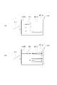
- FIG. 3 is a diagram showing opening/closing control of the gate mechanism.
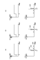
- FIG. 4 is a diagram showing an example of a combined control of the extraction electrode and gate mechanism.
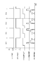
- FIG. 5 is a diagram showing patterns of opening/closing control of the gate mechanism and potential control of the extraction electrode according to the embodiment.
- FIG. 6 is a diagram illustrating multiple event operations according to an embodiment.
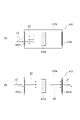
- FIG. 7 is a diagram showing a first modification of the imaging unit.
- FIG. 8 is a diagram showing opening/closing control of the gate mechanism in the first modified example of the imaging unit.
- FIG. 9 is a diagram showing a second modification of the imaging unit.
- the mass spectrometer 1 includes a sample stage 2, an irradiation section 3, an imaging unit 4, a control section 5, a data processing section 6, an extraction electrode 11 (first electrode), and a ground (GND) electrode 12 (second electrode).
- the mass spectrometer 1 uses a laser desorption/ionization (LDI) method, a surface-assisted laser desorption/ionization (SALDI) method, a matrix-assisted laser desorption/ionization (MALDI: Matrix- Assisted Laser Desorption/Ionization) method, secondary ion mass spectrometry (SIMS) method, and other mass spectrometry methods.
- LCI laser desorption/ionization
- SALDI surface-assisted laser desorption/ionization
- MALDI matrix-assisted laser desorption/ionization
- SIMS secondary ion mass spectrometry
- the mass spectrometer 1 may be used for mass spectrometry using an ionization support substrate DIUTHAME manufactured by
- a sample S is placed on the sample stage 2 .
- a support substrate for supporting the sample S for example, the above-described ionization support substrate
- the support substrate is placed on the sample table 2 together with the sample S.
- the sample stage 2 is, for example, a glass substrate on which a transparent conductive film such as an ITO (Indium Tin Oxide) film is formed, and the surface of the transparent conductive film serves as a mounting surface.
- a voltage is applied to the sample stage 2 .
- the sample table 2 may be any member that can ensure conductivity (for example, a substrate made of a metal material such as stainless steel, etc.).
- the sample S is, for example, a biological sample.
- the irradiation unit 3 is arranged on the surface side of the sample table 2 on which the sample S is placed.
- the irradiating unit 3 irradiates a predetermined range of the sample S having a predetermined area with the energy beam L1 all at once.
- the irradiation unit 3 irradiates the sample S with the energy beam L1, which is a flat beam having a spot diameter that includes the predetermined range.
- the size of the spot diameter of the energy beam L1 may be a size that includes the entire sample S to be measured, or may be a size that includes only a portion of the sample S.
- the entire sample S is image can be obtained.
- the energy beam L1 is irradiated, the plurality of components S1 of the sample S within the predetermined range are ionized all at once.
- the irradiation unit 3 ionizes the plurality of components S1 while maintaining the positional information of the sample S in the region irradiated with the energy beam L1. That is, the component S1 of the sample S is ionized by the irradiation of the energy beam L1. As a result, ionized sample S2, which is component S1 of ionized sample S, is generated.
- the sample stage 2 may be fixed by sandwiching both ends (both sides) of the sample stage 2 with metal or the like.
- the irradiation unit 3 may be arranged on the opposite side (back side) of the surface of the sample stage 2 on which the sample S is placed. That is, the irradiation unit 3 may irradiate the sample S with the energy beam L1 from the rear surface side of the sample stage 2 .
- the mass spectrometer 1 is configured as a projection mass spectrometer.
- a signal of one pixel having a size corresponding to the spot diameter of the energy beam is obtained for each energy beam irradiation. That is, in the scanning mass spectrometer, the resolution of the image obtained depends on the spot diameter of the energy beam L1.
- the projection-type mass spectrometer 1 a signal of an image (plurality of pixels) corresponding to the spot diameter of the energy beam L1 is acquired for each irradiation of the energy beam L1. That is, in the projection mass spectrometer, the resolution of the image obtained does not depend on the spot diameter of the energy beam L1. Therefore, according to the mass spectrometer 1, it is possible to obtain an image with higher resolution (spatial resolution) than the scanning mass spectrometer.
- the energy ray L1 is, for example, laser light.
- the energy beam L1 is, for example, an N2 laser, a YAG laser, or the like.
- the intensity distribution of the energy ray L1 (the intensity distribution in the cross section perpendicular to the axis) is substantially uniform.
- the spot diameter of the energy beam L1 is, for example, about 100 ⁇ m to 300 ⁇ m.
- the energy ray L1 may be an electron beam or an ion beam.
- the irradiation unit 3 irradiates the energy beam L1 in pulses.
- the irradiation unit 3 irradiates the energy beam L1 for each event.
- the irradiation unit 3 irradiates the energy beam L1 once in one event. That is, one irradiation of the energy beam L1 corresponds to one event.
- the extraction electrode 11 is arranged at a position facing the surface of the sample stage 2 on which the sample S is placed. That is, the extraction electrode 11 is arranged on the flight path of the ionized sample S2 from the sample table 2 to the imaging unit 4. As shown in FIG.
- the extraction electrode 11 is, for example, a plate-like electrode and has a passage hole 11a for passing the ionized sample S2.
- the sample stage 2 described above functions as a plate-shaped electrode facing the extraction electrode 11 .
- the potential of the extraction electrode 11 is set to be lower than the potential of the sample stage 2 at the time when the irradiation unit 3 irradiates the energy beam L1.
- the ionized sample S2 is pulled out from the surface of the sample S toward the extraction electrode 11 side.
- the extraction electrode 11 extracts the ionized sample S2 from the surface of the sample S by the potential difference between the extraction electrode 11 and the sample stage 2 .
- the potential of the extraction electrode 11 is set to be higher than the potential of the sample stage 2 at the time when the irradiation unit 3 irradiates the energy beam L1.
- the ionized sample S2 is pulled out from the surface of the sample S toward the extraction electrode 11 side.
- the ionized sample S2 is positive ions.
- the direction of changing the level of the potential between the electrodes and the potential of the extraction electrode is opposite to the following explanation.
- the ground electrode 12 is arranged downstream of the extraction electrode 11 in the flight path of the ionized sample S2. Specifically, the ground electrode 12 is arranged between the extraction electrode 11 and a micro-channel plate (hereinafter referred to as "MCP") 41 (electron emitting portion) of the imaging unit 4 .
- MCP micro-channel plate
- the ground electrode 12 is, for example, a plate-like electrode and has a passage hole 12a for passing the ionized sample S2.
- the ground electrode 12 accelerates the ionized sample S2 extracted by the extraction electrode 11 due to the potential difference between the ground electrode 12 and the extraction electrode 11 .
- the potential of the ground electrode 12 is set lower than the potential of the extraction electrode 11, thereby accelerating the ionized sample S2 from the extraction electrode 11 side to the ground electrode 12 side.
- the potential of the ground electrode 12 is set to 0V, for example.
- the imaging unit 4 has an MCP 41 , a phosphor 42 , an imaging section 43 and an optical lens (connecting section) 44 .
- the MCP 41 is arranged downstream of the extraction electrode 11 and the ground electrode 12 in the flight path of the ionized sample S2.
- the flight path of the ionized sample S2 is substantially linear from the sample stage 2 to the MCP 41 , and the MCP 41 is arranged at a position facing the sample stage 2 .
- the flight path of the ionized sample S2 is not limited to such a substantially linear path. That is, the MCP 41 is not necessarily arranged at a position facing the sample stage 2 .
- a trift (TRIFT: triple focusing time-of-flight) in which the trajectory of the ionized sample S2 is bent three times and the ionized sample S2 is flown in a V shape.
- MCP 41 does not face the sample table 2 when a reflectron that causes the ionized sample S2 to fly in a figure-of-eight shape, or the like is used.
- the length of the path from the sample table 2 to the imaging unit 43 (electron or light detection surface) is, for example, about 80 cm.
- the ionized sample S2 accelerated by the sample stage 2, extraction electrode 11, and ground electrode 12 described above flies toward the MCP 41 and collides with the MCP 41.
- a plurality of ionized samples S2 fly while maintaining their positional information, and collide with the MCP 41 with time difference information generated by the mass difference. That is, the ionized sample S2 reaches the MCP 41 at different timings according to the mass difference for each type.
- the MCP 41 emits electrons E (photoelectrons) corresponding to the ionized sample S2.
- the MCP 41 has an input surface 41a facing the sample stage 2 and an output surface 41b opposite to the input surface 41a.
- the MCP 41 outputs electrons E from the output surface 41b in response to incidence of ions (charged particles) on the input surface 41a. That is, the MCP 41 converts the spatial distribution of ions into the spatial distribution of electrons (electron image).
- the MCP 41 has, for example, a plate-like structure in which a plurality of glass capillaries (channels) with inner diameters of several ⁇ m to several tens of ⁇ m are bundled.
- Each channel of MCP 41 functions as an independent secondary electron multiplier. That is, in the MCP 41, ions reaching the surface of the channel are converted into secondary electrons, and the secondary electrons are electron-multiplied while repeating collisions within the channel. The time from ion collision to extraction of secondary electrons is several nanoseconds or less.
- the imaging unit 4 may have a plurality of MCPs 41 .
- the phosphor 42 is arranged behind the MCP 41 . That is, the phosphor 42 is arranged between the MCP 41 and the imaging section 43 on the opposite side of the MCP 41 from the sample stage 2 .
- the phosphor 42 has an input surface 42a facing the MCP 41 and an output surface 42b opposite to the input surface 42a.
- the input surface 42a functions as an electron detection surface.
- the phosphor 42 has a substrate 421 and a phosphor layer 422 .
- the phosphor 42 is arranged such that the phosphor layer 422 faces the MCP 41 .
- the input surface 42a described above is the surface of the fluorescent layer 422 on the MCP 41 side
- the output surface 42b is the surface of the substrate 421 opposite to the MCP 41 side.
- the material of the substrate 421 is, for example, transparent glass.
- the material of substrate 421 is, for example, sapphire.
- the fluorescent layer 422 is applied to the surface of the substrate 421 opposite to the output surface 42b.
- the fluorescent layer 422 is made of a fluorescent material that emits fluorescence when struck by electrons.
- the fluorescent material of the fluorescent layer 422 is, for example, GaN.
- the fluorescent material of fluorescent layer 422 may be, for example, ZnO or a plastic scintillator.
- the fluorescent layer 422 emits fluorescence L2 corresponding to the electrons E emitted from the MCP41.
- the fluorescent layer 422 converts the fluorescent light L2 due to the impingement of the electrons E into a fluorescent pattern (optical image).
- a fluorescent material has an afterglow characteristic that emits light even after the electronic excitation is gone and gradually weakens.
- the afterglow time of the fluorescent layer 422 is, for example, 12 ns or less.
- the afterglow time of the fluorescent layer 422 is, for example, about 3 ns. That is, the phosphor 42 is a so-called high-speed phosphor.
- the MCP 41 and the fluorescent layer 422 are close to each other within a range in which no discharge occurs, and a high voltage is applied to each.
- a high voltage is applied to each.
- signal amplification factor (gain) by causing ions and electrons to collide with the MCP 41 and the fluorescent layer 422 at high speed, both signal amplification factor (gain) and positional information are achieved.
- the fluorescent layer 422 can be formed, for example, by epitaxially growing the fluorescent material on the substrate 421 (eg, sapphire substrate). In this case, the thickness of the fluorescent layer 422 is, for example, about 1 ⁇ m to 5 ⁇ m.
- the fluorescent layer 422 may be formed by coating a powdery fluorescent material made of ZnO, for example, on the substrate 421 (for example, a sapphire substrate). In this case, the thickness of the fluorescent layer 422 is, for example, about 2 ⁇ m to 8 ⁇ m.
- the imaging unit 43 is arranged behind the phosphor 42 . That is, the imaging unit 43 is arranged on the opposite side of the phosphor 42 from the MCP 41 .
- the imaging unit 43 has a solid-state imaging device 431 .
- the solid-state imaging device 431 acquires (captures) an image based on the electrons E emitted from the MCP 41 .
- the electrons E are converted into the fluorescence L2 by the phosphor 42, so the solid-state imaging device 431 acquires (captures) an image based on the fluorescence L2 from the phosphor 42.
- the solid-state imaging device 431 is, for example, a CMOS image sensor.
- the solid-state imaging device 431 may be, for example, a CCD image sensor, a high-speed image sensor, or the like.
- the solid-state imaging device 431 has a gate mechanism 432 .
- the gate mechanism 432 is configured to be switchable between an open state in which an image based on the fluorescence L2 from the phosphor 42 is captured and a closed state in which an image based on the fluorescence L2 from the phosphor 42 is not captured.
- the minimum duration of the open state of the gate mechanism 432 ie, the minimum interval from the closed state to the open state to the closed state again) is about the same as the afterglow time of the fluorescent layer 422 .
- the minimum duration of the open state of the gate mechanism 432 is, for example, about 3 ns.
- the opening/closing timing of the gate mechanism 432 is variable.
- the optical lens 44 is arranged between the phosphor 42 and the imaging section 43 .
- the optical lens 44 optically connects the phosphor 42 and the imaging section 43 .
- the optical lens 44 is connected to the imaging section 43 .
- the optical lens 44 guides the fluorescence L2 from the phosphor 42 to the imaging section 43 .
- the control unit 5 controls the operations of the irradiation unit 3, the extraction electrode 11, and the imaging unit 43.
- the control unit 5 controls the irradiation unit 3 so as to irradiate the energy beam L1 in pulses.
- the control unit 5 controls the potential of the extraction electrode 11 . That is, the controller 5 controls the magnitude of the voltage applied to the extraction electrode 11 .
- the control unit 5 also controls the opening/closing operation of the gate mechanism 432 .
- the control unit 5 controls the imaging unit 43 so as to execute imaging processing.
- the control unit 5 is, for example, a computer device including a processor (eg, CPU, etc.), memory (eg, ROM, RAM, etc.), and the like.
- the data processing unit 6 processes data of images captured by the imaging unit 43 .
- the data processing unit 6 is, for example, a computer device including a processor (eg, CPU, etc.), memory (eg, ROM, RAM, etc.), and the like.
- a processor eg, CPU, etc.
- memory eg, ROM, RAM, etc.
- control unit 5 and the data processing unit 6 are shown separately in the example of FIG. 1, the control unit 5 and the data processing unit 6 may be configured by the same computer device.
- control unit 5 performs Post Extraction Differential Acceleration (PEDA) in order to improve the mass resolution of a predetermined detection target component among the one or more components S1 contained in the sample S. .
- PEDA Post Extraction Differential Acceleration
- FIG. 2 is a diagram schematically showing the above control (PEDA).
- the horizontal axis indicates the position of the ionized sample S2
- the vertical axis indicates the potential applied to each electrode (sample stage 2, extraction electrode 11, and ground electrode 12).
- Two ionized samples 21 and 22 schematically shown in FIG. 2 are ions having the same mass (ions corresponding to the same component S1).
- the control unit 5 raises the potential of the extraction electrode 11 by a predetermined amount at the timing when the ionized samples 21 and 22 corresponding to the component to be detected are positioned between the extraction electrode 11 and the ground electrode 12 . That is, the control unit 5 changes the potential of the extraction electrode 11 from the state shown in FIG. 2(A) to the state shown in FIG. 2(B). As a result, the ionized sample 22 with a lower initial velocity (ie, ions flying at a position farther from the ground electrode 12) than the ionized sample 21 with a higher initial velocity (ie, ions flying at a position closer to the ground electrode 12) is given a larger acceleration energy.
- 2(B) corresponds to the acceleration energy given to the ionized samples 21 and 22 .
- This makes it possible to absorb the time-of-flight difference caused by the difference in initial velocity between the ionized samples 21 and 22 . That is, the timings at which the ionized samples 21 and 22 reach the imaging unit 43 can be brought closer, and the mass resolution of the component S1 corresponding to the ionized samples 21 and 22 can be improved.
- the timing at which the ionized sample S2 corresponding to the component to be detected is positioned between the extraction electrode 11 and the ground electrode 12 can be determined in advance by experiments, simulations, or the like. Alternatively, the timing is determined by the mass-to-charge ratio (m/z) of the ions of the component to be detected, the acceleration voltage of the ions (that is, the potentials set to the sample stage 2, the extraction electrode 11, and the ground electrode 12), and the sample It may be determined by performing a predetermined calculation based on various parameters such as the distance from the base 2 to the extraction electrode 11 and the ground electrode 12 .
- the above timing is, for example, several microseconds after the irradiation of the energy beam L1.
- control unit 5 causes the imaging unit 43 to acquire an image as an analysis target during a period corresponding to the detection target component.
- the period corresponding to the detection target component is a partial period including the timing when the fluorescence L2 corresponding to the detection target component reaches the imaging unit 43 .
- control unit 5 controls the operation of the gate mechanism 432 so that it is open during a specific period corresponding to the component to be detected and is closed during periods other than the specific period.
- the opening/closing control of the gate mechanism 432 will be described with reference to FIG.
- a case where the solid-state imaging device 431 has a housing 431a, a photocathode 431b, and a CMOS image sensor 431c will be described as an example.
- the photocathode 431b is provided on the incident surface of the fluorescence L2 in the housing 431a (that is, the surface facing the optical lens 44).
- the CMOS image sensor 431c is provided at a position facing the photocathode 431b inside the evacuated housing 431a.
- the photocathode 431b emits electrons E1 (photoelectrons) corresponding to the fluorescence L2 incident on the photocathode 431b to the CMOS image sensor 431c in the housing 431a.
- the CMOS image sensor 431c detects electrons E1.
- the gate mechanism 432 is implemented by a photocathode 431b and a CMOS image sensor 431c. Specifically, the opening/closing control of the gate mechanism 432 is realized by controlling the magnitude relationship between the potential of the photocathode 431b and the potential of the CMOS image sensor 431c.
- FIG. 3 shows the closed state.
- the controller 5 makes the potential of the photocathode 431b higher than that of the CMOS image sensor 431c, thereby controlling the electrons E1 emitted from the photocathode 431b not to go to the CMOS image sensor 431c. This achieves the closed state.
- FIG. 3 shows the open state.
- the controller 5 controls the electrons E1 emitted from the photocathode 431b to travel to the CMOS image sensor 431c. This achieves the open state.
- the period corresponding to the component to be detected is determined in advance by experiments, simulations, or the like, similarly to the timing of changing the potential of the extraction electrode 11 described above. can be determined.
- the above period includes the mass-to-charge ratio (m/z) of the ions of the component to be detected, the acceleration voltage of the ions (that is, the potentials set to the sample stage 2, the extraction electrode 11, and the ground electrode 12), and the sample It may be determined by performing a predetermined calculation based on various parameters such as the distance from the base 2 to the extraction electrode 11 and the ground electrode 12 .
- the upper graph shows the potential of the extraction electrode 11 .
- the horizontal axis indicates time with reference (origin) to the point in time when the sample S is irradiated with the energy ray L1 by the irradiation unit 3, and the vertical axis indicates the potential of the extraction electrode 11.
- FIG. The lower graph shows ion signals detected by fluorescence L2 corresponding to three components S10, S20, and S30 contained in the sample S (that is, components having different masses) reaching the imaging unit 43. showing strength.
- the abscissa indicates time with the time point at which the sample S is irradiated with the energy ray L1 by the irradiation unit 3 as a reference (origin), and the ordinate indicates the ion signal intensity.
- the component S10 with the shortest flight time (that is, the earliest arrival time at the imaging unit 43) is set as the component to be detected. It shows an example of control when In this example, as shown in the upper graph, the controller 5 raises the potential of the extraction electrode 11 by a predetermined amount at timing t1 corresponding to the component S10.
- the timing t1 is an arbitrary timing when the ionized sample S2 corresponding to the component S10 is positioned between the extraction electrode 11 and the ground electrode 12.
- the time width for the ionized sample S2 corresponding to the component S10 to reach the imaging unit 43 is the same as when the potential of the extraction electrode 11 is not controlled (for example, in FIG. 4). (B) and (C)). That is, the mass resolution of component S10 can be improved.
- control unit 5 controls the operation of the gate mechanism 432 so that it is open during the period p1 corresponding to the component S10 and closed during periods other than the period p1.
- the dashed-dotted line in the lower graph represents the closed state (the dashed-dotted line is at a low position) and the open state (the dashed-dotted line is at a high position) of the gate mechanism 432 .
- the control unit 5 controls the operation of the gate mechanism 432 so that it is open during the period p1 corresponding to the component S10 and closed during periods other than the period p1.
- the dashed-dotted line in the lower graph represents the closed state (the dashed-dotted line is at a low position) and the open state (the dashed-dotted line is at a high position) of the gate mechanism 432 .
- the period p1 is, for example, a period during which only the fluorescence L2 corresponding to the component S10 can be imaged.
- capturing only the fluorescence L2 corresponding to the component S10 means not only the case where no fluorescence other than the fluorescence L2 corresponding to the component S10 is captured at all, but also the case where other components, together with the component S10, are negligible for measurement. It also includes the case where the corresponding fluorescence (noise) is imaged.
- FIG. 4 shows a control example when the component S20 with the next shortest flight time after the component S10 is set as the component to be detected.
- the controller 5 raises the potential of the extraction electrode 11 by a predetermined amount at timing t2 corresponding to the component S20.
- the timing t2 is a timing later than the timing t1, and is an arbitrary timing when the ionized sample S2 corresponding to the component S20 is positioned between the extraction electrode 11 and the ground electrode 12.
- the time width for the ionized sample S2 corresponding to the component S20 to reach the imaging unit 43 is the same as when the potential of the extraction electrode 11 is not controlled (for example, in FIG. 4).
- control unit 5 controls the operation of the gate mechanism 432 so that the gate mechanism 432 is open during the period p2 corresponding to the component S20 and closed during periods other than the period p2. According to the above control, the same effect as that of the component S10 described with reference to FIG. 4A can be obtained for the component S20.
- FIG. 4 shows a control example when the component S30 with the longest flight time is set as the component to be detected.
- the controller 5 raises the potential of the extraction electrode 11 by a predetermined amount at timing t3 corresponding to the component S30.
- the timing t3 is a timing later than the timing t2, and is an arbitrary timing when the ionized sample S2 corresponding to the component S30 is positioned between the extraction electrode 11 and the ground electrode 12.
- the time width for the ionized sample S2 corresponding to the component S30 to reach the imaging unit 43 is the same as when the potential of the extraction electrode 11 is not controlled (for example, in FIG. 4).
- control unit 5 controls the operation of the gate mechanism 432 so that it is open during the period p3 corresponding to the component S30 and closed during periods other than the period p3. According to the above control, the same effect as the effect of the component S10 described with reference to FIG. 4A can be obtained for the component S30.
- FIG. 5 is a diagram showing patterns of opening/closing control of the gate mechanism 432 and potential control of the extraction electrode 11 according to such an embodiment.
- FIG. 6 is a diagram illustrating multiple event operations according to an embodiment. In the embodiment shown in FIGS. 5 and 6, the mass spectrometer 1 performs mass spectrometry by alternately detecting two types of components S10 and S20 among the components S10, S20 and S30 described above.
- the control unit 5 stores control patterns for the gate mechanism 432 in advance.
- the control pattern of the gate mechanism 432 is, for example, a pattern that defines a period for opening the gate mechanism 432 based on the time when the sample S is irradiated with the energy beam L1.
- the control unit 5 stores in advance a first gate pattern corresponding to the component S10 and a second gate pattern corresponding to the component S20 as control patterns for the gate mechanism 432 .
- the first gate pattern is a pattern that defines that the gate mechanism 432 is opened during the period p1 corresponding to the component S10, and the gate mechanism 432 is closed during periods other than the period p1.
- the second gate pattern is a pattern in which the gate mechanism 432 is opened during the period p2 corresponding to the component S20, and the gate mechanism 432 is closed during periods other than the period p2.
- the control unit 5 stores in advance the potential control pattern of the extraction electrode 11 .
- the potential control pattern of the extraction electrode 11 is, for example, a pattern that determines the timing of increasing the potential of the extraction electrode 11 by a predetermined amount based on the time when the sample S is irradiated with the energy beam L1.
- the control unit 5 stores in advance a first potential pattern corresponding to the component S10 and a second potential pattern corresponding to the component S20 as potential control patterns for the extraction electrode 11 .
- the first potential pattern is a pattern in which the potential of the extraction electrode 11 is increased by a predetermined amount at timing t1 corresponding to the component S10.
- the second potential pattern is a pattern in which the potential of the extraction electrode 11 is increased by a predetermined amount at timing t2 according to the component S20.
- the opening/closing operation of the gate mechanism 432 as described above is, for example, switched between opening and closing based on a voltage signal generated by a function generator (that is, as shown in FIG. can be realized by switching the relationship between high and low potentials.
- the controller 5 uses the irradiation of the energy beam L1 as a trigger to output the H (high) signal and the L (low) signal. It has a counter configured to toggle.
- the control unit 5 causes the irradiating unit 3 to irradiate the energy beam L1 in pulses and causes the counter to count the irradiation of the energy beam L1. Switch to "H ⁇ L" or "L ⁇ H".
- control unit 5 switches between the first gate pattern and the second gate pattern according to the output from the counter. For example, the control unit 5 operates the gate mechanism 432 according to the first gate pattern when the output from the counter switches to the H signal, and operates the gate mechanism 432 based on the time when the output from the counter switches to the L signal.
- the gate mechanism 432 is operated with a two-gate pattern.
- the control unit 5 switches between the first potential pattern and the second potential pattern according to the output from the counter. For example, the control unit 5 controls the potential of the lead-out electrode 11 with the first potential pattern with reference to the point in time when the output from the counter switches to the H signal, and the point in time when the output from the counter switches to the L signal. , the potential of the extraction electrode 11 is controlled by the second potential pattern.
- FIG. 6 shows a case where four events EV1 to EV4 are performed continuously.
- the potential of the extraction electrode 11 is raised at timing t1 corresponding to the component S10,
- the gate mechanism 432 is opened during the period p1 corresponding to the component S10. That is, in events EV1 and EV3, imaging mass spectrometry suitable for component S10 is realized. More specifically, in the events EV1 and EV3, the mass resolution of the component S10 can be improved, and only the data required for the analysis of the component S10 (data corresponding to the period p1) can be acquired once.
- imaging mass spectrometry suitable for component S20 is achieved. More specifically, in the events EV2 and EV4, the mass resolution of the component S20 can be improved, and only the data required for the analysis of the component S20 (data corresponding to the period p2) can be acquired once. It is possible to reduce the amount of information (data amount) acquired and stored in imaging.
- the data processing unit 6 performs processing for superimposing a plurality of images captured by the imaging unit 43 .
- the data processing unit 6 may generate one image by overlapping the images captured in the events EV1 and EV2 described above. Thereby, it is possible to observe images corresponding to the respective components S10 and S20 in the one image. That is, it is possible to confirm the positions of the respective components S10 and S20 in one image.
- the imaging unit 43 may generate a clear image of the component by superimposing (integrating) a plurality of images captured for the same component.
- the data processing unit 6 can obtain a clear image of the component S10 by overlapping the image captured at the event EV1 and the image captured at the event EV3. can. Similarly, the data processing unit 6 can obtain a clear image of the component S20 by superimposing the image captured at the event EV2 and the image captured at the event EV4.
- the mass resolution of the component to be detected can be improved by changing the potential of the extraction electrode 11 . Furthermore, by acquiring an image as an analysis target during a period corresponding to the detection target component (for example, periods p1, p2, p3 corresponding to each component S10, S20, S30 as shown in FIG. 4), one time It is possible to reduce the amount of information (data amount) that is acquired and stored as an analysis target in imaging. As described above, it is possible to improve the processing speed while improving the mass resolution.
- the mass spectrometer 1 is provided with a ground electrode 12 which is arranged between the extraction electrode 11 and the MCP 41 and accelerates the ionized sample S2 extracted by the extraction electrode 11 due to the potential difference with the extraction electrode 11.
- the timing corresponding to the component to be detected may be the timing at which the ionized sample S2 corresponding to the component to be detected is positioned between the extraction electrode 11 and the ground electrode 12 . According to the above configuration, it is possible to reliably improve the mass resolution of the component to be detected.
- the mass spectrometer 1 is arranged between the MCP 41 and the imaging unit 43 and includes a phosphor 42 that emits fluorescence L2 (light) corresponding to the electrons E emitted by the MCP 41 . Also, the imaging unit 43 may acquire an image based on the light from the phosphor 42 . According to the above configuration, a sensor or the like that detects light can be used as the imaging unit 43 .
- the fluorescent material of the phosphor 42 may be GaN, ZnO, or a plastic scintillator. According to the above configuration, the afterglow time of the fluorescent material can be shortened. Therefore, when the interval between the timing at which one component (for example, component S10 in FIG. 4) reaches the imaging unit 43 and the timing at which another component (for example, component S20 in FIG. 4) reaches the imaging unit 43 is short, Also, the phosphor 42 can emit light corresponding to another component without being affected by afterglow corresponding to one component. Thereby, the light corresponding to each component can be emitted with high accuracy, and the accuracy of mass spectrometry can be improved.
- the imaging unit 43 has a gate mechanism 432 configured to switch between an open state in which an image based on the fluorescence L2 from the phosphor 42 is captured and a closed state in which an image based on the fluorescence L2 from the phosphor 42 is not captured.
- the control unit 5 is in an open state during periods corresponding to the components to be detected (for example, periods p1, p2, and p3 corresponding to the respective components S10, S20, and S30 as shown in FIG. 4) and periods other than the above periods.
- the operation of the gate mechanism 432 may be controlled so as to be closed immediately. In this embodiment, as described with reference to FIG.
- the control unit 5 controls the operation of the gate mechanism 432 by switching the potential magnitude relationship between the photocathode 431b and the CMOS image sensor 431c. According to the above configuration, by performing the imaging process only for a period corresponding to the component to be detected by the opening/closing operation of the gate mechanism 432, it is possible to appropriately suppress the amount of information acquired and stored in one imaging.
- the energy ray L1 may be laser light, electron beam or ion beam. According to the above configuration, an appropriate type of energy ray can be selected as required.
- the control unit 5 changes the detection target component for each event, and performs a plurality of events (for example, FIG. 6 , events EV1 to EV4) may be executed.
- a plurality of events for example, FIG. 6 , events EV1 to EV4.
- an image corresponding to the component S10 is acquired in the first and third events EV1 and EV3
- an image corresponding to the component S20 is acquired in the second and fourth events EV2 and EV4.
- Mass spectrometry method Next, a mass spectrometry method using the mass spectrometer 1 will be described.
- the sample S is placed on the sample stage 2 .
- the irradiation unit 3 irradiates the sample S with the energy beam L1 (first step).
- the plurality of components S1 are ionized while maintaining the positional information of the sample S in the irradiation area of the energy beam L1.
- ionized sample S2 which is component S1 of ionized sample S, is generated.
- the ionized sample S2 is pulled out from the surface of the sample S by the potential difference between the sample stage 2 and the extraction electrode 11 (second step).
- a predetermined detection target component here, as an example, component S10
- the potential of the extraction electrode 11 is changed at the corresponding timing t1 (third step).
- the control unit 5 increases the potential of the extraction electrode 11 by a predetermined amount, and when the ionized sample S2 corresponding to the component to be detected is negative ions, The potential of the extraction electrode 11 is lowered by a predetermined amount. As a result, it is possible to reduce variations in the timing at which the ionized sample S2 group related to the detection target component reaches the imaging unit 43, and improve the mass resolution of the detection target component.
- the imaging unit 43 arranged after the MC 41 acquires an image based on the electrons E1 emitted by the MCP 41 (in this embodiment, an image based on the fluorescence L2 converted from the electrons E1 by the phosphor 42).
- the control unit 5 causes the imaging unit 43 to acquire an image as an analysis target during a period p1 corresponding to the detection target component (here, as an example, the component S10).
- the control unit 5 causes the imaging unit 43 to acquire only the image corresponding to the period p1 by opening the gate mechanism 432 only during the period p1.
- the mass resolution of the detection target component is can be improved. Furthermore, by acquiring an image as an analysis target for a period corresponding to the detection target component, it is possible to reduce the amount of information (data volume) acquired and stored as the analysis target in one imaging. As described above, it is possible to improve the processing speed while improving the mass resolution.
- the mass spectrometer 1 changes the component to be detected for each event when the unit of processing from the first step to the fifth step is one event.
- a plurality of events EV1 to EV4 may be executed (while alternately changing the component to be detected between components S10 and S20 in the example of FIG. 6). According to the above configuration, it is possible to acquire an image (imaging mass spectrometry) corresponding to each of a plurality of components while suppressing the amount of information in one event.
- a plurality of events may be executed by storing the potential control pattern of the extraction electrode in advance and switching the control pattern corresponding to each component for each event.
- control by an analog circuit using a counter was exemplified. , microcomputer control, PC control, or the like.
- the configuration of the imaging unit 4 is not limited to the embodiment described above. Modifications of the imaging unit 4 will be described below.
- FIG. 7 is a diagram showing a first modification (imaging unit 4A) of the imaging unit.
- the imaging unit 4A differs from the imaging unit 4 in that it further has an optical relay lens (connecting portion) 45 and an image intensifier 433 .
- the imaging section 43 has a solid-state imaging device 431 and an image intensifier 433 .
- the solid-state imaging device 431 is arranged behind the image intensifier 433 . That is, the solid-state imaging device 431 is arranged on the opposite side of the image intensifier 433 from the phosphor 42 .
- the image intensifier 433 has a gate mechanism 434 .
- the optical relay lens 45 is arranged between the image intensifier 433 and the solid-state imaging device 431 .
- the optical relay lens 45 optically connects the image intensifier 433 and the solid-state imaging device 431 .
- the image intensifier 433 has a housing 433a, a photocathode 433b, an MCP 433c, and a phosphor screen 433d.
- the photocathode 433b is provided on the incident surface of the fluorescence L2 (that is, the surface facing the optical lens 44) in the housing 433a.
- the MCP 433c is provided in a vacuum housing 431a at a position facing the photocathode 433b.
- the phosphor screen 433d is provided on the surface of the housing 433a opposite to the side on which the photocathode 433b is provided (that is, the surface facing the optical relay lens 45).
- the photocathode 433b emits electrons E2 (photoelectrons) corresponding to the fluorescence L2 incident on the photocathode 433b to the MCP 433c inside the housing 433a.
- the MCP 433c multiplies the electron E2.
- the fluorescent screen 433d converts the electrons E3 multiplied by the MCP 433c into fluorescence L3, and emits the fluorescence L3 to the solid-state imaging device 431 side.
- the gate mechanism 434 of the image intensifier 433 is realized by the photocathode 433b and the MCP 433c. Specifically, the opening/closing control of the gate mechanism 434 is realized by controlling the magnitude relationship between the potential of the photocathode 433b and the potential of the MCP 433c.
- FIG. 8 shows the closed state.
- the controller 5 makes the potential of the photocathode 433b higher than that of the MCP 433c, thereby controlling the electrons E2 emitted from the photocathode 433b not to go toward the MCP 433c.
- the controller 5 sets the potential of the MCP 433c to 0V and sets the potential of the photocathode 433b to 30V. This achieves the closed state.
- FIG. 8 shows the open state.
- the controller 5 controls the electrons E2 emitted from the photocathode 433b to travel to the MCP 433c.
- the controller 5 sets the potential of the MCP 433c to 0V and sets the potential of the photocathode 433b to -200V. This achieves the open state.
- the gate mechanism 434 of the image intensifier 433 may be used to perform opening/closing control as shown in FIG.
- the fluorescence L2 from the phosphor 42 can be amplified by the image intensifier 433, and the solid-state imaging element 431 can image. Therefore, even when the fluorescence L2 from the phosphor 42 is extremely weak, the fluorescence L2 can be imaged.
- the switching speed of the gate mechanism 434 of the image intensifier 433 is faster than that of the mechanical gate mechanism. Therefore, by using the gate mechanism 434 of the image intensifier 433, the timing at which one component (for example, the component S10 shown in FIG. 4) reaches the imaging unit 43 and the other component (for example, the timing shown in FIG. Even when the interval between the timing at which the component S20) reaches the imaging unit 43 is short, the images corresponding to the respective components can be suitably separated and captured.
- FIG. 9 is a diagram showing a second modification (imaging unit 4B) of the imaging unit.
- the imaging unit 4B differs from the imaging unit 4 in that it has an electronic sensor 435 as the imaging section 43 instead of the phosphor 42, the optical lens 44, and the solid-state imaging device 431.
- FIG. The electronic sensor 435 is a detector that has the function of detecting electron energy. In the imaging unit 4B, the electron E emitted by the MCP 41 can be directly detected by the electronic sensor 435, so the phosphor 42 can be omitted.
- control unit 5 controls the period corresponding to the component to be detected in the image acquired by the electronic sensor 435 (for example, the periods p1 and p2 corresponding to the components S10, S20, and S30 shown in FIG. 4). , p3) may be acquired and stored as an analysis target. As a result, the amount of information (data amount) acquired and stored as an analysis target in one imaging can be reduced.
- the solid-state imaging device 431 may be a camera (for example, an event-driven camera, a high-speed video camera, etc.) that does not include the gate mechanism 432.
- the control unit 5 controls the period corresponding to the component to be detected in the image acquired by the solid-state imaging device 431 (for example, the period p1, S20, S30 shown in FIG. Data on the images acquired in p2 and p3) may be acquired and stored as analysis targets. As a result, the amount of information (data amount) acquired and stored as an analysis target in one imaging can be reduced.
- an FOP fiber optical plate
- the FOP may be directly connected to the output surface 42b of the substrate 421 of the phosphor 42.
- an FOP may be used instead of the optical relay lens 45 in the imaging unit 4A.
Landscapes
- Chemical & Material Sciences (AREA)
- Analytical Chemistry (AREA)
- Physics & Mathematics (AREA)
- Optics & Photonics (AREA)
- Spectroscopy & Molecular Physics (AREA)
- Other Investigation Or Analysis Of Materials By Electrical Means (AREA)
- Analysing Materials By The Use Of Radiation (AREA)
- Sampling And Sample Adjustment (AREA)
Abstract
Description
図1に示されるように、質量分析装置1は、試料台2と、照射部3と、撮像ユニット4と、制御部5と、データ処理部6と、引出電極11(第1電極)と、グランド(GND)電極12(第2電極)と、を備えている。質量分析装置1は、レーザ脱離イオン化(Laser Desorption/Ionization、LDI)法、表面支援レーザ脱離イオン化(SALDI:Surface-Assisted Laser Desorption/Ionization)法、マトリックス支援レーザ脱離イオン化(MALDI:Matrix-Assisted Laser Desorption/Ionization)法、2次イオン質量分析(SIMS)法等の質量分析法に用いられる。また、質量分析装置1は、浜松ホトニクス社製のイオン化支援基板DIUTHAME(ジュテーム)を用いた質量分析法に用いられてもよい。
次に、質量分析装置1を用いた質量分析方法について説明する。まず、図1に示されるように、試料Sを試料台2に載置する。続いて、照射部3によって、試料Sに対してエネルギー線L1を照射する(第1ステップ)。これにより、エネルギー線L1の照射領域における試料Sの位置情報を維持したまま複数の成分S1をイオン化する。その結果、イオン化された試料Sの成分S1であるイオン化試料S2が発生する。
以上、本開示の一実施形態について説明したが、本開示は、上記実施形態に限られない。各構成の材料及び形状には、上述した材料及び形状に限らず、様々な材料及び形状を採用することができる。
図7は、撮像ユニットの第1変形例(撮像ユニット4A)を示す図である。撮像ユニット4Aは、光学リレーレンズ(接続部)45と、イメージインテンシファイア433を更に有している点で撮像ユニット4と相違している。撮像ユニット4Aでは、撮像部43は、固体撮像素子431とイメージインテンシファイア433と、を有している。固体撮像素子431は、イメージインテンシファイア433の後段に配置されている。つまり、固体撮像素子431は、イメージインテンシファイア433に対して蛍光体42とは反対側に配置されている。イメージインテンシファイア433は、ゲート機構434を有している。光学リレーレンズ45は、イメージインテンシファイア433と固体撮像素子431との間に配置されている。光学リレーレンズ45は、イメージインテンシファイア433及び固体撮像素子431を光学的に接続している。
図9は、撮像ユニットの第2変形例(撮像ユニット4B)を示す図である。撮像ユニット4Bは、蛍光体42、光学レンズ44、及び固体撮像素子431の代わりに、撮像部43としての電子センサ435を有している点で撮像ユニット4と相違している。電子センサ435は、電子のエネルギーを検出する機能を有する検出器である。撮像ユニット4Bでは、MCP41により放出された電子Eを、電子センサ435によって直接検出することができるため、蛍光体42を省略することができる。この場合、制御部5は、電子センサ435によって取得される画像のうち、検出対象成分に応じた期間(例えば、図4に示されるような各成分S10,S20,S30に応じた期間p1,p2,p3)に取得された画像に関するデータを分析対象として取得及び保存すればよい。これにより、1回の撮像において分析対象として取得及び保存される情報量(データ量)を低減できる。
また、撮像ユニット4において、固体撮像素子431は、ゲート機構432を備えないカメラ(例えば、イベント駆動カメラ、高速度ビデオカメラ等)であってもよい。この場合、制御部5は、固体撮像素子431によって取得される画像のうち、検出対象成分に応じた期間(例えば、図4に示されるような各成分S10,S20,S30に応じた期間p1,p2,p3)に取得された画像に関するデータを分析対象として取得及び保存すればよい。これにより、1回の撮像において分析対象として取得及び保存される情報量(データ量)を低減できる。
Claims (10)
- 試料が載置される試料台と、
前記試料に対してエネルギー線を照射し、前記エネルギー線が照射される領域における前記試料の位置情報を維持したまま前記試料の成分をイオン化する照射部と、
前記照射部によりイオン化された前記試料の成分であるイオン化試料を、前記試料台との電位差によって前記試料の表面から引き出す第1電極と、
前記イオン化試料の飛行経路において前記第1電極よりも下流に配置され、前記イオン化試料に応じた電子を放出する電子放出部と、
前記電子放出部の後段に配置され、前記電子放出部により放出された電子に基づく画像を取得する撮像部と、
前記照射部、前記第1電極、及び前記撮像部の動作を制御する制御部と、を備え、
前記制御部は、前記照射部による前記エネルギー線の照射後、前記試料に含まれる一以上の成分のうちの所定の検出対象成分に応じたタイミングで前記第1電極の電位を変化させると共に、前記検出対象成分に応じた期間に分析対象としての前記画像を前記撮像部に取得させ、
前記制御部は、前記タイミングにおいて、前記検出対象成分に対応する前記イオン化試料が正イオンの場合には前記第1電極の電位を所定量上げ、前記検出対象成分に対応する前記イオン化試料が負イオンの場合には前記引出電極の電位を所定量下げる、質量分析装置。 - 前記第1電極と前記電子放出部との間に配置され、前記第1電極との電位差によって、前記第1電極により引き出された前記イオン化試料を加速させる第2電極を更に備え、
前記検出対象成分に応じた前記タイミングは、前記検出対象成分に対応する前記イオン化試料が前記第1電極と前記第2電極との間に位置するタイミングである、請求項1に記載の質量分析装置。 - 前記電子放出部と前記撮像部との間に配置され、前記電子放出部により放出された前記電子に応じた光を発する蛍光体を更に備え、
前記撮像部は、前記蛍光体からの前記光に基づく画像を取得する、請求項1又は2に記載の質量分析装置。 - 前記蛍光体の蛍光材料は、GaN、ZnO又はプラスチックシンチレータである、請求項3に記載の質量分析装置。
- 前記撮像部は、前記蛍光体からの前記光に基づく画像を撮像する開状態と前記蛍光体からの前記光に基づく画像を撮像しない閉状態とを切替可能に構成されたゲート機構を有し、
前記制御部は、前記検出対象成分に応じた前記期間に開状態となり前記期間以外の期間に閉状態となるように、前記ゲート機構の動作を制御する、請求項3又は4に記載の質量分析装置。 - 前記撮像部は、前記ゲート機構を有するイメージインテンシファイアと、前記イメージインテンシファイアの後段に配置される固体撮像素子と、を有する、請求項5に記載の質量分析装置。
- 前記エネルギー線は、レーザ光、電子ビーム又はイオンビームである、請求項1~6のいずれか一項に記載の質量分析装置。
- 前記制御部は、前記照射部による前記エネルギー線の1回の照射に対応する処理単位を1イベントとした場合に、1イベント毎に前記検出対象成分を変更しながら、複数のイベントを実行する、請求項1~7のいずれか一項に記載の質量分析装置。
- エネルギー線を照射する照射部によって、試料に対して前記エネルギー線を照射することで、前記エネルギー線が照射される領域における前記試料の位置情報を維持したまま前記試料の成分をイオン化する第1ステップと、
前記試料が載置される試料台と第1電極との電位差によって、前記照射部によりイオン化された前記試料の成分であるイオン化試料を前記試料の表面から引き出す第2ステップと、
前記照射部による前記エネルギー線の照射後、前記試料に含まれる一以上の成分のうちの所定の検出対象成分に応じたタイミングで前記第1電極の電位を変化させる第3ステップと、
前記イオン化試料の飛行経路において前記第1電極よりも下流に配置された電子放出部に、前記イオン化試料に応じた電子を放出させる第4ステップと、
前記電子放出部の後段に配置された撮像部に、前記電子放出部により放出された電子に基づく画像を取得させる第5ステップと、を含み、
前記第3ステップにおいて、前記検出対象成分に対応する前記イオン化試料が正イオンの場合には前記第1電極の電位を所定量上げ、前記検出対象成分に対応する前記イオン化試料が負イオンの場合には前記引出電極の電位を所定量下げ、
前記第5ステップにおいて、前記検出対象成分に応じた期間に、分析対象としての前記画像を前記撮像部に取得させる、質量分析方法。 - 前記第1ステップから前記第5ステップまでの処理単位を1イベントとした場合に、1イベント毎に前記検出対象成分を変更しながら、複数の前記イベントを実行する、請求項9に記載の質量分析方法。
Priority Applications (4)
| Application Number | Priority Date | Filing Date | Title |
|---|---|---|---|
| IL305218A IL305218A (en) | 2021-02-22 | 2021-12-06 | Mass spectrometry device and mass spectrometry method |
| CN202180094318.9A CN116888466A (zh) | 2021-02-22 | 2021-12-06 | 质量分析装置及质量分析方法 |
| EP21926748.1A EP4279898A4 (en) | 2021-02-22 | 2021-12-06 | Mass spectrometry device and mass spectrometry method |
| US18/277,643 US20240234119A9 (en) | 2021-02-22 | 2021-12-06 | Mass spectrometry device and mass spectrometry method |
Applications Claiming Priority (2)
| Application Number | Priority Date | Filing Date | Title |
|---|---|---|---|
| JP2021-026072 | 2021-02-22 | ||
| JP2021026072A JP2022127858A (ja) | 2021-02-22 | 2021-02-22 | 質量分析装置及び質量分析方法 |
Publications (1)
| Publication Number | Publication Date |
|---|---|
| WO2022176322A1 true WO2022176322A1 (ja) | 2022-08-25 |
Family
ID=82931326
Family Applications (1)
| Application Number | Title | Priority Date | Filing Date |
|---|---|---|---|
| PCT/JP2021/044751 Ceased WO2022176322A1 (ja) | 2021-02-22 | 2021-12-06 | 質量分析装置及び質量分析方法 |
Country Status (7)
| Country | Link |
|---|---|
| US (1) | US20240234119A9 (ja) |
| EP (1) | EP4279898A4 (ja) |
| JP (1) | JP2022127858A (ja) |
| CN (1) | CN116888466A (ja) |
| IL (1) | IL305218A (ja) |
| TW (1) | TW202234462A (ja) |
| WO (1) | WO2022176322A1 (ja) |
Families Citing this family (1)
| Publication number | Priority date | Publication date | Assignee | Title |
|---|---|---|---|---|
| EP4397466A4 (en) | 2021-08-31 | 2025-09-03 | Canon Kk | UNFOAMISHED MOLDED BODY CONTAINING POLYURETHANE |
Citations (6)
| Publication number | Priority date | Publication date | Assignee | Title |
|---|---|---|---|---|
| JPS63266751A (ja) * | 1987-04-23 | 1988-11-02 | Jeol Ltd | 静電補正飛行時間型二次イオン顕微鏡 |
| JP2010251174A (ja) | 2009-04-17 | 2010-11-04 | Osaka Univ | イオン源、質量分析装置、制御装置、制御方法、制御プログラムおよび記録媒体 |
| JP2011175898A (ja) * | 2010-02-25 | 2011-09-08 | Shimadzu Corp | 飛行時間型質量分析装置 |
| JP2013041699A (ja) * | 2011-08-12 | 2013-02-28 | Shimadzu Corp | 飛行時間型質量分析装置 |
| US9048075B1 (en) * | 2014-01-14 | 2015-06-02 | Shimadzu Corporation | Time-of-flight type mass spectrometer |
| JP2016001531A (ja) * | 2014-06-11 | 2016-01-07 | 株式会社東芝 | 質量分析装置および質量分析方法 |
Family Cites Families (8)
| Publication number | Priority date | Publication date | Assignee | Title |
|---|---|---|---|---|
| US8309913B2 (en) * | 2006-10-03 | 2012-11-13 | Academia Sinica | Angled dual-polarity mass spectrometer |
| GB0918629D0 (en) * | 2009-10-23 | 2009-12-09 | Thermo Fisher Scient Bremen | Detection apparatus for detecting charged particles, methods for detecting charged particles and mass spectometer |
| JP5993678B2 (ja) * | 2012-09-14 | 2016-09-14 | 日本電子株式会社 | マスイメージング装置及びマスイメージング装置の制御方法 |
| US9524855B2 (en) * | 2014-12-11 | 2016-12-20 | Thermo Finnigan Llc | Cascaded-signal-intensifier-based ion imaging detector for mass spectrometer |
| CN110914952B (zh) * | 2017-05-12 | 2022-09-23 | 诺威量测设备公司 | 质谱仪检测器及使用其的系统和方法 |
| JP7174663B2 (ja) * | 2019-04-01 | 2022-11-17 | 浜松ホトニクス株式会社 | イオン検出器 |
| US11854777B2 (en) * | 2019-07-29 | 2023-12-26 | Thermo Finnigan Llc | Ion-to-electron conversion dynode for ion imaging applications |
| JP7424578B2 (ja) * | 2020-01-31 | 2024-01-30 | 浜松ホトニクス株式会社 | 撮像ユニット、質量分析装置、及び質量分析方法 |
-
2021
- 2021-02-22 JP JP2021026072A patent/JP2022127858A/ja active Pending
- 2021-12-06 IL IL305218A patent/IL305218A/en unknown
- 2021-12-06 EP EP21926748.1A patent/EP4279898A4/en not_active Withdrawn
- 2021-12-06 CN CN202180094318.9A patent/CN116888466A/zh active Pending
- 2021-12-06 WO PCT/JP2021/044751 patent/WO2022176322A1/ja not_active Ceased
- 2021-12-06 US US18/277,643 patent/US20240234119A9/en active Pending
- 2021-12-15 TW TW110146891A patent/TW202234462A/zh unknown
Patent Citations (6)
| Publication number | Priority date | Publication date | Assignee | Title |
|---|---|---|---|---|
| JPS63266751A (ja) * | 1987-04-23 | 1988-11-02 | Jeol Ltd | 静電補正飛行時間型二次イオン顕微鏡 |
| JP2010251174A (ja) | 2009-04-17 | 2010-11-04 | Osaka Univ | イオン源、質量分析装置、制御装置、制御方法、制御プログラムおよび記録媒体 |
| JP2011175898A (ja) * | 2010-02-25 | 2011-09-08 | Shimadzu Corp | 飛行時間型質量分析装置 |
| JP2013041699A (ja) * | 2011-08-12 | 2013-02-28 | Shimadzu Corp | 飛行時間型質量分析装置 |
| US9048075B1 (en) * | 2014-01-14 | 2015-06-02 | Shimadzu Corporation | Time-of-flight type mass spectrometer |
| JP2016001531A (ja) * | 2014-06-11 | 2016-01-07 | 株式会社東芝 | 質量分析装置および質量分析方法 |
Non-Patent Citations (2)
| Title |
|---|
| ANONYMOUS: "Technologies and products for recycling sorting equipment catalog", RECYCLING SORTING EQUIPMENT CATALOG, 1 August 2020 (2020-08-01), JP, pages 1 - 20, XP009539057 * |
| See also references of EP4279898A4 |
Also Published As
| Publication number | Publication date |
|---|---|
| CN116888466A (zh) | 2023-10-13 |
| IL305218A (en) | 2023-10-01 |
| EP4279898A1 (en) | 2023-11-22 |
| EP4279898A4 (en) | 2025-01-01 |
| US20240234119A9 (en) | 2024-07-11 |
| JP2022127858A (ja) | 2022-09-01 |
| US20240136170A1 (en) | 2024-04-25 |
| TW202234462A (zh) | 2022-09-01 |
Similar Documents
| Publication | Publication Date | Title |
|---|---|---|
| CN1773268B (zh) | 离子束系统和用于检测离子束的系统 | |
| JP5521177B2 (ja) | 質量分析装置 | |
| JP5403509B2 (ja) | イオン源および質量分析装置 | |
| JP2013101918A (ja) | 質量分析装置 | |
| JP2015514300A (ja) | 質量分析/質量分析データを並列取得するための方法および装置 | |
| JP2015514300A5 (ja) | ||
| JP5504969B2 (ja) | 質量分析装置 | |
| WO2022176322A1 (ja) | 質量分析装置及び質量分析方法 | |
| CN117912933A (zh) | 一种获取等离子体初始能量分布状态的装置 | |
| JP7424578B2 (ja) | 撮像ユニット、質量分析装置、及び質量分析方法 | |
| JP6666626B2 (ja) | 荷電粒子検出器及び荷電粒子線装置 | |
| JP5582493B2 (ja) | マイクロチャネルプレート組立体及びマイクロチャネルプレート検出器 | |
| WO2013073373A1 (en) | Mass distribution spectrometry method and mass distribution spectrometer | |
| JP5979075B2 (ja) | 飛行時間型質量分析装置 | |
| JP6938297B2 (ja) | 質量分析装置および質量分析方法 | |
| JP7479859B2 (ja) | 質量分析装置、及び質量分析方法 | |
| CN109860014B (zh) | 一种快速成像质谱仪 | |
| EP1630851A2 (en) | A detector for a co-axial bipolar time-of-flight mass spectrometer | |
| Yoshimura et al. | Evaluation of a delay-line detector combined with analog-to-digital converters as the ion detection system for stigmatic imaging mass spectrometry | |
| JP3055160B2 (ja) | 中性粒子質量分析装置 | |
| JPH0619973B2 (ja) | 静電補正飛行時間型二次イオン顕微鏡 | |
| JP2000182557A (ja) | 荷電粒子線装置 |
Legal Events
| Date | Code | Title | Description |
|---|---|---|---|
| 121 | Ep: the epo has been informed by wipo that ep was designated in this application |
Ref document number: 21926748 Country of ref document: EP Kind code of ref document: A1 |
|
| WWE | Wipo information: entry into national phase |
Ref document number: 305218 Country of ref document: IL |
|
| WWE | Wipo information: entry into national phase |
Ref document number: 18277643 Country of ref document: US |
|
| WWE | Wipo information: entry into national phase |
Ref document number: 202180094318.9 Country of ref document: CN |
|
| ENP | Entry into the national phase |
Ref document number: 2021926748 Country of ref document: EP Effective date: 20230818 |
|
| NENP | Non-entry into the national phase |
Ref country code: DE |
|
| WWW | Wipo information: withdrawn in national office |
Ref document number: 2021926748 Country of ref document: EP |