WO2022181400A1 - ガスセンサ - Google Patents
ガスセンサ Download PDFInfo
- Publication number
- WO2022181400A1 WO2022181400A1 PCT/JP2022/005989 JP2022005989W WO2022181400A1 WO 2022181400 A1 WO2022181400 A1 WO 2022181400A1 JP 2022005989 W JP2022005989 W JP 2022005989W WO 2022181400 A1 WO2022181400 A1 WO 2022181400A1
- Authority
- WO
- WIPO (PCT)
- Prior art keywords
- oxide
- nanowire
- gas sensor
- pad electrode
- substrate
- Prior art date
- Legal status (The legal status is an assumption and is not a legal conclusion. Google has not performed a legal analysis and makes no representation as to the accuracy of the status listed.)
- Ceased
Links
Images







Classifications
-
- G—PHYSICS
- G01—MEASURING; TESTING
- G01N—INVESTIGATING OR ANALYSING MATERIALS BY DETERMINING THEIR CHEMICAL OR PHYSICAL PROPERTIES
- G01N27/00—Investigating or analysing materials by the use of electric, electrochemical, or magnetic means
- G01N27/02—Investigating or analysing materials by the use of electric, electrochemical, or magnetic means by investigating impedance
- G01N27/04—Investigating or analysing materials by the use of electric, electrochemical, or magnetic means by investigating impedance by investigating resistance
-
- G—PHYSICS
- G01—MEASURING; TESTING
- G01N—INVESTIGATING OR ANALYSING MATERIALS BY DETERMINING THEIR CHEMICAL OR PHYSICAL PROPERTIES
- G01N27/00—Investigating or analysing materials by the use of electric, electrochemical, or magnetic means
- G01N27/02—Investigating or analysing materials by the use of electric, electrochemical, or magnetic means by investigating impedance
- G01N27/04—Investigating or analysing materials by the use of electric, electrochemical, or magnetic means by investigating impedance by investigating resistance
- G01N27/12—Investigating or analysing materials by the use of electric, electrochemical, or magnetic means by investigating impedance by investigating resistance of a solid body in dependence upon absorption of a fluid; of a solid body in dependence upon reaction with a fluid, for detecting components in the fluid
- G01N27/125—Composition of the body, e.g. the composition of its sensitive layer
- G01N27/127—Composition of the body, e.g. the composition of its sensitive layer comprising nanoparticles
-
- H—ELECTRICITY
- H10—SEMICONDUCTOR DEVICES; ELECTRIC SOLID-STATE DEVICES NOT OTHERWISE PROVIDED FOR
- H10D—INORGANIC ELECTRIC SEMICONDUCTOR DEVICES
- H10D62/00—Semiconductor bodies, or regions thereof, of devices having potential barriers
- H10D62/10—Shapes, relative sizes or dispositions of the regions of the semiconductor bodies; Shapes of the semiconductor bodies
- H10D62/117—Shapes of semiconductor bodies
- H10D62/118—Nanostructure semiconductor bodies
- H10D62/119—Nanowire, nanosheet or nanotube semiconductor bodies
- H10D62/121—Nanowire, nanosheet or nanotube semiconductor bodies oriented parallel to substrates
Definitions
- the present invention relates to a gas sensor that combines a nanowire made of a specific metal and an oxide made of a high-resistance semiconductor.
- Non-Patent Document 1 describes a gas sensor in which a first pad electrode, a second pad electrode, and platinum nanowires connecting these pad electrodes are formed on a glass substrate.
- hydrogen gas is detected based on a change in resistance detected between the first pad electrode and the second pad electrode while a constant voltage is applied between the first pad electrode and the second pad electrode. is detected.
- JP 2015-137998 A Japanese Patent Application Laid-Open No. 2003-149189
- An oxygen gas sensor using a solid electrolyte such as that described in Patent Document 1 requires a reference gas, is not sufficiently sensitive to oxygen, and has a slow response speed (a response time of about several tens of seconds). have.
- a resistive oxygen gas sensor using an oxide semiconductor as described in Patent Document 2 can also obtain a response speed of 10 seconds or less when the operating temperature is extremely high such as 900° C. or 600° C. When the operating temperature is a relatively low temperature of about 300° C., the response time is several hundred seconds or more, and the response speed is so slow that it cannot be said to meet the needs of the industry.
- Non-Patent Document 1 detects hydrogen gas, but does not describe detection of oxygen gas. In other words, the sensor characteristics such as response speed and sensitivity to oxygen gas have not been verified at all.
- an object of the present invention is to provide a gas sensor with a high response speed and high sensitivity to oxygen gas.
- the present inventors conceived of a gas sensor that combines a nanowire made of a specific metal such as platinum (Pt) and an oxide layer made of a specific high-resistance semiconductor.
- a gas sensor that combines a nanowire made of a specific metal such as platinum (Pt) and an oxide layer made of a specific high-resistance semiconductor.
- Pt platinum
- an oxide layer made of a high-resistance semiconductor By arranging the nanowire in contact with an oxide layer made of a high-resistance semiconductor, in addition to the first conduction path for carriers (oxygen vacancies, electrons, etc.) to pass through the nanowire, carriers (oxygen vacancies, electrons, etc.) electrons, etc.) are injected from the nanowire into the oxide layer, travel through the oxide layer, and form a second conduction path that travels back to the nanowire again.
- the present inventors have found that the presence of these two conduction paths can provide remarkable effects of high response speed and high sensitivity to oxygen gas.
- the high resistance semiconductor constituting the oxide layer is cerium oxide, tin oxide, zirconium oxide, zinc oxide, tungsten oxide, iron oxide, nickel oxide, cerium-zirconium oxide, titanium oxide, cobalt oxide, oxide.
- the substrate is any one of a glass substrate, an alumina substrate, a zirconia substrate, and a silicon substrate having a silicon oxide film formed thereon. gas sensor.
- the gas sensor of the present invention has a fast response speed and high sensitivity to oxygen gas.
- FIG. 1 is a schematic perspective view of a gas sensor 100 according to one embodiment of the invention
- FIG. 2 is a schematic top view of the gas sensor 100
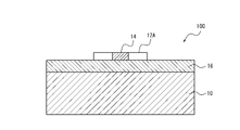
- FIG. FIG. 1B is a cross-sectional view taken along line II of FIG. 1B
- FIG. 1B is a cross-sectional view taken along the line II-II of FIG. 1B
- (A) to (E) are diagrams for explaining the manufacturing process of the gas sensor 100 according to one embodiment of the present invention.
- 5 is a graph showing changes over time in current I in Experimental Example 1.
- FIG. 9 is a graph showing changes over time in current I in Experimental Example 2.
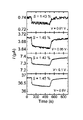
- FIG. 5 is a graph showing changes over time in current I in Experimental Example 1.
- FIG. 10 is a graph showing changes over time in current I in Experimental Example 3.
- FIG. 10 is a graph showing changes over time in current I in Experimental Example 4.
- FIG. 10 is a graph showing changes over time in current I in Experimental Example 4.
- FIG. 10 is a graph showing changes over time in current I in Experimental Example 5.
- FIG. 10 is a graph showing changes over time in current I in Experimental Example 5.
- FIG. 10 is a graph showing changes over time in current I in Experimental Example 6.
- FIG. 10 is a graph showing changes over time in current I in Experimental Example 7.
- FIG. 10 is a graph showing changes over time in current I in Experimental Example 8.
- FIG. 11 is a graph showing changes over time in current I in Experimental Example 9.
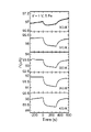
- FIG. (A) and (B) are graphs showing temporal changes in current I in Experimental Example 10.
- FIG. 10 is a graph showing changes over time in current I in Experimental Example 11.
- FIG. 10 is a graph showing changes over time in current I in Experimental Example 11.
- FIG. 10 is a graph showing changes
- a gas sensor 100 includes a substrate 10, first pad electrodes 12A and second pad electrodes 12B, and nanowires made of a specific metal. 14 and an oxide layer 16 made of a high resistance semiconductor.
- the first pad electrode 12A and the second pad electrode 12B are formed on or above the substrate 10 .
- a nanowire 14 is formed on or above the substrate 10 to connect the first pad electrode 12A and the second pad electrode 12B.
- An oxide layer 16 is formed in contact with the nanowires 14 .
- the contact between the nanowires 14 and the oxide layer 16 realizes high-speed response and high sensitivity to oxygen gas.
- a formed on or above B means that A is formed directly on B or indirectly via another layer.
- a current is passed between the first pad electrode 12A and the second pad electrode 12B, and the gas is detected based on the change in the electric signal detected between the first pad electrode 12A and the second pad electrode 12B.
- a power supply 18 and an ammeter 20 are connected in series between the first pad electrode 12A and the second pad electrode 12B, and a voltmeter 22 is connected in parallel.
- the power source 18 applying a constant voltage between the first pad electrode 12A and the second pad electrode 12B
- the current between the first pad electrode 12A and the second pad electrode 12B is measured by the ammeter 20.
- a change is detected and gas is detected based on the detected change in current.
- Gas can also be detected. Gas can also be detected based on the change in resistance detected between the first pad electrode 12A and the second pad electrode 12B instead of the change in current or voltage. That is, the above “electrical signal” means current, voltage, or resistance.
- the circuit of the gas sensor can be configured with two terminals, so the gas sensor can be constructed without increasing wiring and circuits.
- the type of gas detected in this embodiment is not particularly limited, this embodiment is suitable for detecting oxygen gas.
- the substrate 10 supports the first pad electrode 12A and the second pad electrode 12B, as well as the nanowires 14 and the oxide layer 16 that serve as the gas detector.
- the substrate 10 is not particularly limited as long as it has an insulating surface.
- it may be an insulating substrate such as a glass substrate, an alumina substrate, or a zirconia substrate, or a silicon substrate having a silicon oxide film formed on its surface. can be used.
- the shape and dimensions of the substrate 10 are not particularly limited, but when using a substrate having a rectangular main surface shape, the dimensions are, for example, length: 10 to 300 mm x width: 10 to 300 mm x thickness: 0.3 to 1.2 mm. can be in the range of
- the first pad electrode 12A and the second pad electrode 12B are a pair of electrodes necessary for supplying current to the nanowires 14 and detecting changes in electrical signals corresponding to changes in gas concentration.
- the shape and dimensions of the first pad electrode 12A and the second pad electrode 12B are not particularly limited as long as they are formed on or above the insulating surface of the substrate 10. The dimensions may be, for example, length: 30-500 ⁇ m ⁇ width: 30-500 ⁇ m ⁇ thickness: 10-500 nm.
- the metal forming the first pad electrode 12A and the second pad electrode 12B is not particularly limited, and may be any metal, but from the viewpoint of process simplicity, it is preferably the same metal as the nanowire described later. .
- the nanowire 14 connects the first pad electrode 12A and the second pad electrode 12B and is one of the elements constituting the gas detection part formed on or above the insulating surface of the substrate 10.
- platinum (Pt), palladium (Pd), and at least one selected from alloys thereof are preferable, and platinum (Pt) and at least one selected from these alloys are most preferable.
- These elements used for the nanowires 14 are platinum group elements and function as catalysts.
- a platinum group element as a catalyst has the effect of activating the gas, promoting the adsorption of the gas and the chemical reaction between the oxide and the gas, increasing the amount of adsorbed oxygen, and increasing oxygen ions. These catalytic effects improve the sensitivity of the gas response.
- the shape of the nanowires 14 is not particularly limited, the cross-sectional shape perpendicular to the extending direction of the nanowires 14 is preferably rectangular, as shown in FIG. 1D.
- the line width W of the nanowires 14 is not particularly limited as long as it is on the order of nm (that is, less than 1 ⁇ m), but from the viewpoint of sufficiently achieving high-speed response and high sensitivity to oxygen gas, it is preferably 150 nm or less, and 50 nm or less. and more preferably 30 nm or less.
- the lower limit of the line width W of the nanowires 14 is not particularly limited because the narrower the line width W of the nanowires 14, the better from the viewpoint of high-speed response and high sensitivity.
- the line width W of the nanowires 14 is preferably 5 nm or more.
- the thickness of the nanowires 14 is not particularly limited, it is preferably 20 nm or less, more preferably 10 nm or less, from the viewpoint of sufficiently achieving high-speed response and high sensitivity to oxygen gas. Also, the thickness of the nanowires 14 is preferably as thin as possible from the viewpoint of high-speed response and high sensitivity, so the lower limit is not particularly limited. However, the thickness of the nanowires 14 is preferably 1 nm or more from the viewpoint of process constraints and electrical conduction as nanowires.
- the cross-sectional area perpendicular to the extending direction of the nanowires 14 is not particularly limited, it is preferably 3,000 nm 2 or less, and 1,500 nm 2 or less from the viewpoint of sufficiently realizing high-speed response and high sensitivity to oxygen gas. is more preferably 1000 nm 2 or less, even more preferably 600 nm 2 or less, even more preferably 500 nm 2 or less, and even more preferably 300 nm 2 or less.
- the cross-sectional area perpendicular to the extending direction of the nanowires 14 is preferably as small as possible from the viewpoint of high-speed response and high sensitivity, so the lower limit is not particularly limited. However, due to process restrictions, the cross-sectional area perpendicular to the extending direction of the nanowires 14 is preferably 15 nm 2 or more.
- the length L of the nanowires 14 is not particularly limited, it is preferably 80 nm or more, more preferably 400 nm or more, from the viewpoint of sufficiently achieving high-speed response and high sensitivity to oxygen gas.
- the length L of the nanowires 14 is preferably as long as possible from the viewpoint of high-speed response and high sensitivity, so the upper limit is not particularly limited. However, due to process constraints, the length L of the nanowires 14 is preferably 1 m or less.
- the oxide layer 16 consists of a high resistance semiconductor and is in contact with the nanowires 14 .
- this nanowire 14/oxide layer 16 contact achieves high-speed response and high sensitivity to oxygen gas.
- the nanowires 14/oxide layer 16 contact may be such that the oxide layer 16 is (I) located between the insulating surface of the substrate 10 and the nanowires 16 and in contact with the bottom surface of the nanowires 14, or (II) It is essential to fill at least one or both of: located on the nanowires 14 and in contact with the top surface of the nanowires 14 .
- this embodiment relates to aspect (I) above, wherein an oxide layer 16 is located (on) on the insulating surface of the substrate 10, and on the oxide layer 16 (on), a first pad Electrodes 12A and second pad electrodes 12B and nanowires 14 are located.
- the present invention is not limited to this, and may also relate to the above aspect (II).
- An oxide layer 16 may be formed on this nanowire 14 .
- Aspects (I) and (II) above include cases in which the nanowires 14 are embedded in the oxide layer 16, and cases in which the oxide layer 16 is in contact with the side surfaces of the nanowires 14 in addition to the top and bottom surfaces. .
- the high-resistance semiconductor forming the oxide layer 16 may be an oxide semiconductor having a resistivity of 1 ⁇ m or more and 100000 ⁇ m or less at 300° C.
- oxide semiconductor having a resistivity of 1 ⁇ m or more and 100000 ⁇ m or less at 300° C.
- CeO 2 cerium oxide
- SnO 2 tin oxide
- the oxide semiconductor may be an oxide having a non-stoichiometric composition as well as an oxide having a stoichiometric composition, and may include an oxide having a different oxidation number.
- Oxygen is adsorbed on the surface of the oxide semiconductor forming the oxide layer 16 .
- the adsorbed oxygen withdraws electrons from the oxide semiconductor to become oxygen ions such as O 2 ⁇ and O 2 ⁇ .
- Oxygen ions O ⁇ and O 2 ⁇ have a negative charge, so in the case of an n-type semiconductor, the surface is depleted and the electrical conductivity decreases, and in the case of a p-type semiconductor, the carrier concentration increases and the electrical conductivity increases. do.
- the high resistance semiconductor (oxide semiconductor) forming the oxide layer 16 is an oxide of a metal different from the metal forming the nanowires 14 .
- Activation energies exist in each process of adsorption, generation, and annihilation of oxygen/oxygen ions, as well as generation and annihilation of oxygen vacancies, and these activation energies depend on the oxide semiconductor. .
- the oxide semiconductor is an oxide of the metal that constitutes the nanowires 14, such as the combination of Pt/ PtO2 , the activation energy is high, the response time and recovery time of the gas sensor are slow, and the sensitivity is low.
- the oxide semiconductor is an oxide of a metal different from the metal forming the nanowires 14, the activation energy is low, so the response time and recovery time of the gas sensor are shortened, and the sensitivity is increased.
- the thickness of the oxide layer 16 is not particularly limited, it is preferably 5 nm or more from the viewpoint of sufficiently achieving high-speed response and high sensitivity to oxygen gas.
- the upper limit of the thickness of the oxide layer 16 in the position of the aspect (I) is not particularly limited.
- the thickness of the material layer 16 is preferably 100 nm or less.
- the upper limit of the thickness of the oxide layer 16 at the position (II) is not particularly limited. Therefore, the thickness of the oxide layer 16 is preferably 100 nm or less.
- oxygen vacancies oxygen vacancies
- This oxygen-deficient site traps electrons and acts as a donor site that releases the electrons.
- the electrons released from this oxygen deficiency are supplied to the conductor and become carriers to conduct band conduction, or conduct hopping conduction between oxygen deficiency sites.
- the metals (Pt, Pd, etc.) that make up the nanowires contribute to the reduction of the activation energy that generates oxygen defects through their catalytic action, making it easier for oxygen defects to occur. Furthermore, the activation energy of electron transfer (charge injection) at the interface between metal and oxide is lowered to reduce the height of the Schottky barrier existing between metal and oxide. Oxygen defects increase the carrier density in the vicinity of the interface, and thus contribute to reducing the width of the Schottky barrier to several tens of nanometers or less. Both the reduction in barrier height by catalysis and the increase in carrier density by oxygen vacancies reduce the resistance based on the Schottky barrier between metal and oxide, enabling ohmic contact. At the interface with ohmic contact, the resistance is almost constant regardless of the electric field at the interface, and electron transfer at the metal/oxide interface is less likely to be hindered.
- Atoms of the metal (Pt, Pd, etc.) in contact with the oxide relatively easily diffuse into the oxide when the metal is vapor-deposited on the oxide or annealed at several hundred degrees centigrade. is atomically doped.
- the catalytic activity is much higher compared to the bulk metal.
- the higher catalytic activity makes oxygen defects more likely to occur, lower barrier heights, and narrower barrier widths due to increased carrier concentration, as compared to undoped oxides. It becomes thin easily.
- the doping of metal atoms into oxides improves the gas sensor response due to the susceptibility to the generation of oxygen defects, forms ohmic contacts and reduces ohmic resistance, and improves the conductivity of electrons in oxides. contribute to the improvement of
- Electrons injected from the metal into the oxide through the ohmic contact at the metal/oxide interface can flow through the oxide through band conduction or hopping conduction and return to the nanowire making the ohmic contact.
- a voltage is applied across the nanowire where the metal nanowire and the oxide are in contact, electron conduction in the metal occurs within the metal nanowire.
- the electron conduction through the conduction path in which the charge injected from the metal to the oxide conducts through the oxide and returns to the metal is added. Since the current flowing through the bypass circuit through this oxide strongly depends on the oxygen defect concentration, the gas sensor response becomes highly sensitive.
- the contact resistance does not depend on the electric field, so the electron injection frequency between metal and oxide does not depend on the voltage applied to the wire end. This leads to the result of the present invention that the same gas sensor response is obtained even at an applied voltage of, for example, several tens of mV, as at high applied voltages.
- the surface scattering at the metal/oxide contact interface becomes dependent on the oxygen defect concentration that changes the barrier height and barrier width of the Schottky interface.
- a gas sensor using changes in the surface scattering frequency of electrical conduction of metal nanowires, and the present invention is different from surface scattering caused by oxidation on the surface of a single metal as described above, and surface scattering contributed by oxygen deficiency of oxides. Therefore, the surface scattering mechanism in electrical conduction is different.
- the response speed to oxygen gas is fast (that is, the response time is short and the recovery time is short), and the sensitivity is high.
- the gas sensor 100 of the present embodiment has the effect of being able to detect oxygen gas even when the operating temperature is low (for example, about 60 to 300.degree. C.).
- the gas sensor 100 of the present embodiment can detect oxygen gas even when the oxygen gas concentration is low, it has the effect of widening the range of detectable oxygen gas concentrations.
- oxide layer 16 is formed on substrate 10 .
- a precursor solution of an oxide that forms the oxide layer 16 is prepared, this precursor solution is applied onto the substrate 10, and then the substrate 10 is subjected to heat treatment.
- cerium oxide (CeO 2 ) layer cerium acetate hydrate Ce(CH 3 CO 2 ) 3 ⁇ xH 2 O is dissolved in propionic acid to form a cerium oxide (CeO 2 ) precursor of a predetermined concentration.
- a solution can be made.
- Cerium oxide ( CeO2) cerium acetate hydrate Ce ( CH3CO2 ) 3.xH2O ; cerium nitrate hexahydrate Ce[ NO3 ] 3.6H2O ; cerium acetylacetonate hydrate Ce [ C5H7O2 ] 3.xH2O _
- Zirconium oxide ( ZrO2) zirconium (IV) butoxide Zr( OC4H9 ) 4 ; zirconium ( IV ) isopropoxide isopropanol complex Zr(OCH( CH3 ) 2 ) 4.
- the solvent one or more selected from propionic acid, 2-methoxyethanol (CH 3 OCH 2 CH 2 OH), and 1-butanol (C 4 H 9 OH) can be used.
- concentration of the precursor solution is not particularly limited, it is preferably about 0.05 to 0.5 mol/kg depending on the desired film thickness.
- the coating method is not particularly limited, but a spin coating method can be preferably used. The number of revolutions in that case may be appropriately determined according to the desired thickness, and may be in the range of 1000 to 4000 rpm, for example.
- the oxide layer 16 is required to have two functions of electrical conductivity and gas permeability.
- the heat treatment is preferably carried out in an air atmosphere at an ambient temperature in the range of 250 to 800° C. for 0.5 to 2 hours. Note that the thickness of the oxide layer 16 may be adjusted by performing a combination of coating and heat treatment multiple times.
- a resist film 30 is formed on the oxide layer 16.
- the resist film 30 can be formed by applying a photoresist composition for electron beam exposure onto the oxide layer 16 and drying it.
- the coating method is not particularly limited, but a spin coating method can be preferably used.
- the thickness of the resist film 30 is appropriately set so as to be thicker than the thickness of the nanowires 14 to be formed (thicker than both when the nanowires 14 and the pad electrodes 12A and 12B are formed at once). You can set it.
- the resist film 30 is developed to form a mask pattern 32 having a predetermined shape.
- the mask pattern 32 is produced by exposing the resist film 30 by electron beam lithography and developing it.
- the shape of the mask pattern 32 may be appropriately set according to the line width W and length L of the nanowires 14 to be formed.
- the shape of the mask pattern 32 is the nanowires 14 to be formed and the pad electrodes 12A and 12B. can be determined according to the dimensions of The oxide layer 16 is exposed in the portions of the mask pattern 32 where the resist film has been removed.
- a metal film 34 is formed by, for example, electron beam evaporation or sputtering.
- the first portion 34A of the metal film is formed on the mask pattern 32, and the second portion 34B of the metal film is formed on the oxide layer 16 in the portion of the mask pattern 32 where the resist film has been removed.
- the metal film 34 may include a Ti layer having a thickness of about 1 to 5 nm, and a layer made of metal (for example, Pt) forming the nanowires 14 and the pad electrodes 12A and 12B formed thereon.
- the Ti layer functions as an adhesion layer for adhering metal layers constituting the nanowires 14 and the pad electrodes 12A and 12B onto the oxide layer 16.
- a Cr layer may be used as the adhesive layer instead of the Ti layer.
- the nanowires 14 and the pads are formed on the oxide layer 16 by a lift-off process that removes the mask pattern 32 and removes the first portion 34A of the metal film formed thereon. Electrodes 12A and 12B are formed.
- the nanowires 14 and the pad electrodes 12A and 12B are formed together.
- the Ti layer or Cr layer is formed as an adhesion layer for bonding the nanowires 14 onto the oxide layer 16, but in the process of vapor deposition of the metal that constitutes the nanowires 14, Ti or Cr is deposited on the metal layer. diffusing into, most of the Ti layer or Cr layer disappears. Between the oxide layer 16 and the nanowires 14, although island-like Ti or Cr remains at some locations, the oxide layer 16 and the nanowires 14 are in direct contact with each other at most locations, forming an ohmic contact. is doing.
- the gas sensor 100 can be manufactured through the above steps.
- the nanowire 14/oxide layer 16 contact mode is related to (I) above.
- nanowires 14/oxidation A gas sensor in which the contact mode of the material layer 16 is the above (II) can be produced.
- the oxide layer 16 is also formed on the pad electrodes 12A and 12B.
- the oxide layer 16 on the pad electrodes 12A, 12B is removed by, for example, argon sputtering, reactive ion etching, physical scratching, etc., so that electrical contact can be made from the pad electrodes 12A, 12B. There is a need to.
- a gas sensor was produced by the following procedure. First, a Si substrate (length: 15 mm, width: 15 mm, thickness: 0.5 mm) having a surface layer of about 1 ⁇ m made of SiO 2 was prepared.
- cerium acetate hydrate Ce(CH 3 CO 2 ) 3 ⁇ xH 2 O (manufactured by Sigma-Aldrich, 99.9%) was dissolved in propionic acid (manufactured by Wako Chemical Co., Ltd.) to obtain 0.4 mol/ kg of cerium oxide (CeO 2 ) precursor solution was made. After mixing, the precursor solution was stirred on a hot plate (110° C.) at 1000 rpm for 30 minutes to obtain a clear and homogeneous solution. The solution was then passed through a 0.2 ⁇ m PTFE syringe filter and stored at 4°C.
- a cerium oxide (CeO 2 ) layer (thickness: : 28 nm).
- the resistivity of cerium oxide (CeO 2 ) at 300° C. is 200 ⁇ m.
- Pt nanowires were formed on the CeO 2 layer using an electron beam lithography system EBL (Elionix ELS-7500EX). Specifically, an electron beam resist ZEP-520A was applied onto the CeO 2 layer by spin coating, and then a mask pattern having a predetermined shape was drawn with an EBL apparatus. After that, a Ti layer (thickness: 3 nm) and a Pt layer (thickness: 10 nm) were formed thereon by an electron beam evaporation method.
- EBL electron beam lithography system
- Pt nanowires (line width W: 8 nm, line thickness: 10 nm, line length L: 416 nm, cross-sectional shape perpendicular to the line: rectangular) were formed on the CeO2 layer. .
- the Ti layer is formed as an adhesive layer for bonding the Pt nanowires onto the CeO2 layer. part disappears. Between the CeO 2 layer and the Pt nanowires, although island-like Ti remains at some locations, the CeO 2 layer and the Pt nanowires are in direct contact at most locations, forming an ohmic contact. That is, the CeO2 layer is located between the substrate and the Pt nanowires and is in contact with the lower surface of the Pt nanowires.
- a first pad electrode and a second pad electrode (150 ⁇ m ⁇ 150 ⁇ m) each comprising a Ti layer (thickness: 5 nm) and a Pt layer (thickness: 40 nm) thereon were formed. was made. Thus, a gas sensor combining CeO 2 layers and Pt nanowires was fabricated.
- the operating temperature T was set to 300° C. (573 K).
- the oxygen gas was ON, the oxygen gas pressure was changed from 10 ⁇ 3 Pa (vacuum) to 5 Pa, and when the oxygen gas was OFF, the oxygen gas pressure was returned from 5 Pa to 10 ⁇ 3 Pa (vacuum). That is, the oxygen pressure PO2 was set to 5 Pa.
- No carrier gas was introduced into the measurement chamber, and only oxygen gas was introduced. The oxygen gas was turned ON at 0 seconds and turned OFF at 300 seconds.
- FIG. 4 is a graph showing changes in current I over time.
- I Current value at a certain time
- I 0 Initial current value
- I 01 Initial current value (current value when oxygen gas is ON)
- I 02 initial current value (current value when oxygen gas is OFF)
- I s Saturation current value
- I s1 Saturation current value (after oxygen gas ON)
- I s2 saturation current value (after oxygen gas is turned off)
- ⁇ I 1 I 01 -I s1
- I 2 I 02 -I s2
- Sensitivity S (%) ( ⁇ I 1 /I 01 ) x 100
- Response time t res Time required for the current value I to change from the initial current value I01 by 90 % of ⁇ I1
- Recovery time t rec The time required for the current value I to change from the initial current value I02 by 90% of ⁇ I2 .
- the current value after 300 seconds have elapsed is regarded as the saturation current value.
- the response time t res was 21 seconds
- the recovery time t rec was 20 seconds
- a high-speed response to oxygen gas could be realized.
- the sensitivity S was 2.4%, and high sensitivity to oxygen gas could be realized.
- FIG. 5 is a graph showing changes over time in the current I at each level. Table 1 shows the sensor performance at each level.
- FIG. 6 is a graph showing changes over time in the current I at each level. Table 2 shows the sensor performance at each level.
- 7A and 7B are graphs showing changes over time in current I at each level. Also, the sensitivity S at each level is shown in the graph.
- the response time and recovery time do not depend on the applied voltage V.
- the sensitivity S does not depend on the applied voltage V, and has almost the same value between 1.42% and 1.56%.
- a response is observed even when the applied voltage V is 10 mV. Therefore, the gas sensor of this experimental example can sufficiently operate even if the applied voltage is as low as 10 mV, if measures are taken to reduce noise. This contributes to the realization of a gas sensor with low power consumption.
- FIG. 9 is a graph showing changes over time in the current I at each level. Table 4 shows the sensor performance at each level.
- the sensitivity S depends on the oxygen pressure, and the higher the oxygen pressure, the higher the sensitivity.
- response time and recovery time are less dependent on oxygen pressure. Also, a response was obtained even at an oxygen pressure of 0.1 Pa, indicating that the detectable range of oxygen gas concentration is wide.
- FIG. 10 is a graph showing changes over time in current I at each level. The sensitivity S calculated from FIG. 10 was 3.8% at a thickness of 3 nm, 2.5% at a thickness of 6 nm, and 3.6% at a thickness of 10 nm.
- the sensitivity S does not depend much on the Pt thickness. If the line thickness of the Pt nanowires is less than 1 nm, electrical conduction as the Pt nanowires cannot be obtained, so the line thickness is preferably 1 nm or more.
- FIG. 11 is a graph showing changes over time in current I at each level. From FIG. 11 it can be seen that the response and recovery times are independent of the thickness of the CeO 2 layer. Moreover, the sensitivity S calculated from FIG. 11 was 2.5% for both levels. From this it can be seen that the sensitivity S does not depend on the thickness of the CeO2 layer.
- Example 9 A gas sensor was fabricated under the same conditions as in Experimental Example 1, except that the order of forming the CeO 2 layers and the Pt nanowires was reversed. That is, first, as in Experimental Example 1, a Si substrate having a surface layer made of SiO 2 was prepared. Subsequently, Pt nanowires were formed on the SiO 2 layer using an electron beam lithography system EBL (ELS-7500EX manufactured by Elionix). Specifically, an electron beam resist ZEP-520A was applied onto the SiO 2 layer by a spin coating method, and then a mask pattern having a predetermined shape was drawn with an EBL apparatus.
- EBL electron beam lithography system
- a Ti layer (thickness: 3 nm) and a Pt layer (thickness: 10 nm) were formed thereon by an electron beam evaporation method.
- Pt nanowires (line width W: 8 nm, line thickness: 10 nm, line length L: 416 nm, cross-sectional shape perpendicular to the line: rectangular) were formed on the SiO2 layer.
- the Ti layer is formed as an adhesion layer for adhering the Pt nanowires onto the SiO2 layer.
- a first pad electrode and a second pad each consisting of a Ti layer (thickness: 5 nm) and a Pt layer (thickness: 40 nm) thereon are formed on the SiO2 layer. Electrodes (150 ⁇ m ⁇ 150 ⁇ m) were fabricated.
- the precursor solution was applied by spin-coating at 4000 rpm so as to cover the SiO2 layer, Pt nanowires, and the first and second pad electrodes of the substrate, followed by rapid thermal processing equipment (RTA).
- RTA rapid thermal processing equipment
- a cerium oxide ( CeO2) layer (thickness: 28 nm) to cover the SiO2 layer of the substrate, the Pt nanowires, and the first and second pad electrodes by heat-treating at 400°C for 1 hour using formed.
- the Pt nanowires are embedded in the CeO2 layer. That is, the CeO2 layer is located on the Pt nanowires and in contact with the top surface of the Pt nanowires. The CeO2 layer also contacts the sides of the Pt nanowires.
- the CeO2 layer and the Pt nanowires form an ohmic contact.
- FIG. 12 is a graph showing changes in current I over time.
- the response time t res was 25 seconds and the recovery time t rec was 68 seconds or more, and high-speed response to oxygen gas could be realized.
- the sensitivity S was 1.5%, and high sensitivity to oxygen gas could be realized.
- FIG. 13A is a graph showing changes in current I over time.
- the response time t res was 12 seconds
- the recovery time t rec was 8 seconds
- high-speed response to oxygen gas could be realized.
- the sensitivity S was 2.3%, and high sensitivity to oxygen gas could be realized.
- FIG. 13B is a graph showing changes in the current I over time.
- the response time t res was 12 seconds, and it was able to respond to oxygen gas at high speed, but the recovery time t rec was as long as 2 hours or longer.
- the sensitivity S was 97%, and high sensitivity to oxygen gas could be realized.
- the SnO 2 layer was formed by the following procedure. Tin (II) acetylacetonate C 10 H 14 O 4 Sn (manufactured by Sigma-Aldrich, 99.9%) was dissolved in propionic acid (manufactured by Wako Chemical Co., Ltd.) to obtain 0.4 mol/kg of tin oxide (SnO 2 ) A precursor solution was prepared. After mixing, the precursor solution was stirred on a hot plate (110° C.) at 1000 rpm for 30 minutes to obtain a clear and homogeneous solution. The solution was then passed through a 0.2 ⁇ m PTFE syringe filter and stored at 4°C.
- the precursor solution was applied onto the substrate by spin coating at 3000 rpm, and then heat-treated at 300° C. for 1 hour using a rapid thermal processing apparatus (RTA) to form a tin oxide (SnO 2 ) layer (thickness: thickness: 30 nm).
- RTA rapid thermal processing apparatus
- the resistivity of tin oxide (SnO 2 ) at 300° C. is 10 ⁇ m.
- the ZrO 2 layer was formed by the following procedure. Sputtering was performed in an Ar atmosphere using a sputtering target made of ZrO 2 to form a zirconium oxide (ZrO 2 ) layer (thickness: 30 nm) on the substrate.
- ZrO 2 zirconium oxide
- the resistivity of zirconium oxide (ZrO 2 ) at 300° C. is 80000 ⁇ m.
- FIG. 14 is a graph showing changes in current I over time. From this experimental example, it can be seen that oxygen gas can be detected even in an environment where a carrier gas exists.
- the gas sensor of the present invention has a fast response speed and high sensitivity to oxygen gas, so it may be applied to oxygen sensors and breath sensors for internal combustion engines.
- REFERENCE SIGNS LIST 100 gas sensor 10 substrate 12A first pad electrode 12B second pad electrode 14 nanowire 16 oxide layer 18 power supply 20 ammeter 22 voltmeter 30 resist film 32 mask pattern 34 metal film 34A first portion of metal film 34B second portion of metal film
Landscapes
- Chemical & Material Sciences (AREA)
- Chemical Kinetics & Catalysis (AREA)
- Electrochemistry (AREA)
- Physics & Mathematics (AREA)
- Health & Medical Sciences (AREA)
- Life Sciences & Earth Sciences (AREA)
- Analytical Chemistry (AREA)
- Biochemistry (AREA)
- General Health & Medical Sciences (AREA)
- General Physics & Mathematics (AREA)
- Immunology (AREA)
- Pathology (AREA)
- Engineering & Computer Science (AREA)
- Nanotechnology (AREA)
- Investigating Or Analyzing Materials By The Use Of Fluid Adsorption Or Reactions (AREA)
Abstract
Description
[1]絶縁表面を有する基板と、
前記基板の前記絶縁表面上(on or above)に形成された、第1パッド電極及び第2パッド電極と、
前記第1パッド電極と前記第2パッド電極とを連結し、前記基板の前記絶縁表面上(on or above)に形成された、白金(Pt)、パラジウム(Pd)、ロジウム(Rh)、ルテニウム(Ru)、オスミウム(Os)、イリジウム(Ir)、及びこれらの合金から選ばれた一種以上からなるナノワイヤと、
前記ナノワイヤと接触した、前記ナノワイヤを構成する金属とは異種の金属の酸化物の高抵抗半導体からなる酸化物層であって、(I)前記基板の前記絶縁表面と前記ナノワイヤとの間に位置し、前記ナノワイヤの下面と接触する、又は、(II)前記ナノワイヤ上(on)に位置し、前記ナノワイヤの上面と接触する、の一方又は両方を少なくとも満たす酸化物層と、
を有し、
前記第1パッド電極と前記第2パッド電極との間に電流を流し、前記第1パッド電極と前記第2パッド電極との間で検出される電気信号の変化に基づいて、ガスを検出するガスセンサ。
図1A、図1B、図1C及び図1Dを参照して、本発明の一実施形態によるガスセンサ100は、基板10と、第1パッド電極12A及び第2パッド電極12Bと、特定の金属からなるナノワイヤ14と、高抵抗半導体からなる酸化物層16と、を有する。第1パッド電極12A及び第2パッド電極12Bは、基板10上(on or above)に形成される。ナノワイヤ14は、第1パッド電極12Aと第2パッド電極12Bとを連結し、基板10上(on or above)に形成される。酸化物層16は、ナノワイヤ14と接触するように形成される。詳細な作用効果は後述するが、本実施形態では、このナノワイヤ14/酸化物層16の接触により、酸素ガスに対する高速応答及び高感度が実現される。なお、本明細書において「A formed on or above B」とは、B上に直接に、又は、間に別の層を介して間接的にAが形成されることを意味するものとする。
ガスセンサ100では、第1パッド電極12Aと第2パッド電極12Bとの間に電流を流し、第1パッド電極12Aと第2パッド電極12Bとの間で検出される電気信号の変化に基づいて、ガスを検出する。例えば図1Bに示すように、第1パッド電極12Aと第2パッド電極12Bとの間に、直列に電源18及び電流計20を接続し、これと並列に電圧計22を接続する。この場合、電源18によって、第1パッド電極12Aと第2パッド電極12Bとの間に定電圧を印加した状態で、電流計20によって、第1パッド電極と第2パッド電極との間における電流の変化を検出し、検出される電流の変化に基づいて、ガスが検出される。あるいは、第1パッド電極12Aと第2パッド電極12Bとの間に定電流を流した状態で、第1パッド電極12Aと第2パッド電極12Bとの間で検出される電圧の変化に基づいて、ガスを検出することもできる。また、上記の電流又は電圧の変化に代えて、第1パッド電極12Aと第2パッド電極12Bとの間との間で検出される抵抗の変化に基づいて、ガスを検出することもできる。すなわち、上記の「電気信号」とは、電流、電圧、又は抵抗を意味する。本実施形態では、2端子でガスセンサの回路を構成できるので、配線や回路を増やすことがなく、ガスセンサを構築できる。本実施形態において検出されるガスの種類は特に限定されないが、本実施形態は酸素ガスを検出するのに好適である。
基板10は、第1パッド電極12A及び第2パッド電極12B、並びに、ガス検出部となるナノワイヤ14及び酸化物層16を支持する。基板10は、絶縁表面を有するものであれば、特に限定されないが、例えば、ガラス基板、アルミナ基板、ジルコニア基板などの絶縁性基板や、酸化シリコン膜が表面に形成されたシリコン基板などのいずれかを用いることができる。基板10の形状及び寸法は特に限定されないが、主表面形状が矩形である基板を用いる場合、寸法は例えば、縦:10~300mm×横:10~300mm×厚さ:0.3~1.2mmの範囲とすることができる。
第1パッド電極12A及び第2パッド電極12Bは、ナノワイヤ14に電流を供給し、かつ、ガスの濃度変化に対応した電気信号の変化を検出するために必要な一対の電極である。第1パッド電極12A及び第2パッド電極12Bは、基板10の絶縁表面上(on or above)に形成される限り、その形状及び寸法は特に限定されないが、主表面の形状を矩形とする場合、寸法は例えば、縦:30~500μm×横:30~500μm×厚さ:10~500nmの範囲とすることができる。第1パッド電極12A及び第2パッド電極12Bを構成する金属は、特に限定されず、任意の金属であってよいが、プロセス簡易性の観点から、後述のナノワイヤと同種の金属であることが好ましい。
ナノワイヤ14は、第1パッド電極12Aと第2パッド電極12Bとを連結し、基板10の絶縁表面上(on or above)に形成される、ガス検出部を構成する要素の一つである。ナノワイヤ14は、白金(Pt)、パラジウム(Pd)、ロジウム(Rh)、ルテニウム(Ru)、オスミウム(Os)、イリジウム(Ir)、及びこれらの合金から選ばれた一種以上からなることが肝要であり、その中でも、白金(Pt)、パラジウム(Pd)、及びこれらの合金から選ばれた一種以上からなることが好ましく、白金(Pt)及びこの合金から選ばれた一種以上からなることが最も好ましい。ナノワイヤ14に用いられるこれらの元素は、白金族元素であり触媒として機能する。触媒としての白金族元素は、ガスを活性化し、ガスの吸着及び酸化物とガスとの化学反応を促進させ、吸着する酸素量を増やして、酸素イオンを増大させる効果がある。これらの触媒効果により、ガス応答の感度が向上する。
酸化物層16は、高抵抗半導体からなり、ナノワイヤ14と接触している。本実施形態は、このナノワイヤ14/酸化物層16の接触により、酸素ガスに対する高速応答及び高感度が実現される。ナノワイヤ14/酸化物層16の接触態様としては、酸化物層16が、(I)基板10の絶縁表面とナノワイヤ16との間に位置し、ナノワイヤ14の下面と接触する、又は、(II)ナノワイヤ14上(on)に位置し、ナノワイヤ14の上面と接触する、の一方又は両方を少なくとも満たすことが肝要である。
既述のとおり、本実施形態では、ナノワイヤ14と酸化物層16とが接触していること、具体的にはオーミック接触を形成していることが肝要である。これにより、ナノワイヤ14中をキャリア(酸素空孔、電子等)が通過する第1の伝導パスに加えて、キャリア(酸素空孔、電子等)がナノワイヤ14から酸化物層16に注入され、酸化物層16中を移動し、再びナノワイヤ14に戻る経路の第2の伝導パスが形成される。この2つの伝導パスの存在によって、酸素ガスに対して応答速度が速く、感度が高いという顕著な効果を得ることができる。
以上のとおり、本実施形態のガスセンサ100によれば、酸素ガスに対して応答速度が速く(すなわち、応答時間が短く、回復時間が短い)、さらに、感度が高いとの効果を奏する。また、本実施形態のガスセンサ100は、動作温度が低くても(例えば60~300℃程度)酸素ガスが検出できるとの効果も有する。また、本実施形態のガスセンサ100は、酸素ガス濃度が低くても酸素ガスを検出可能であることから、検出可能な酸素ガス濃度の範囲が広いとの効果も有する。
図2(A)~(E)を参照して、本実施形態のガスセンサ100を製造するための好適な方法を説明する。
酸化セリウム(CeO2):酢酸セリウム水和物Ce(CH3CO2)3・xH2O;硝酸セリウム6水和物Ce[NO3]3・6H2O;セリウムアセチルアセトネート水和物Ce[C5H7O2]3・xH2O
酸化スズ(SnO2):無水塩化スズ(II)SnCl2:スズ(II)アセチルアセトネートC10H14O4Sn;スズ(IV)tert-ブトキシドSn[OC(CH3)3]4
酸化ジルコニウム(ZrO2):ジルコニウム(IV)ブトキシドZr(OC4H9)4;ジルコニウム(IV)イソプロポキシドイソプロパノール錯体Zr(OCH(CH3)2)4・(CH3)2CHOH;オキシ硝酸ジルコニウム(IV)水和物ZrO(NO3)2・xH2O
酸化亜鉛(ZnO):硝酸亜鉛6水和物Zn[NO3]2・6H2O;亜鉛(II)アセチルアセトネートC10H14O4Zn;酢酸亜鉛2水和物Zn[CH3COO]2・2H2O
酸化タングステン(WO3):塩化タングステン(VI)WCl6;タングステン(VI)エトキシドC12H30O6W
酸化鉄(Fe2O3):硝酸鉄9水和物Fe[NO3]3・9H2O;酢酸鉄(II)Fe[CO2CH3]2;鉄(III)アセチルアセトネートFe[C5H7O2]3
酸化ニッケル(NiO):ニッケル(II)アセチルアセトネートNi(C5H7O2)2;酢酸ニッケル(II)4水和物Ni[OCOCH3]2・4H2O;硝酸ニッケル(II)6水和物Ni[NO3]2・6H2O
セリウム-ジルコニウム酸化物(CeZrO4):酢酸セリウム水和物Ce(CH3CO2)3・xH2O;ジルコニウム(IV)ブトキシドZr(OC4H9)4
酸化チタン(TiO2):チタン(IV)イソプロポキシドTi[OCH(CH3)2]4;チタン(IV)ブトキシドTi(OCH2CH2CH2CH3)4
酸化コバルト(Co3O4):硝酸コバルト6水和物Co[NO3]2・6H2O;コバルト(II)アセチルアセトネートCo(C5H7O2)2;酢酸コバルト(II)[CH3CO2]2Co;塩化コバルト(II)CoCl2
酸化ニオブ(Nb2O5):塩化ニオブ(V)NbCl5;ニオブ(V)エトキシドNb(OCH2CH3)5;ニオブn-ブトキシドC20H45NbO5
酸化タンタル(Ta2O5):タンタル(V)エトキシドTa(OC2H5)5;タンタル(V)テトラエトキシド2,4-ペンタンジオネートC13H27O6Ta;塩化タンタル(V)TaCl5
酸化ロジウム(Rh2O3):酢酸ロジウム(II)ダイマーRh2(OOCCH3)4;硝酸ロジウム(III)水和物N3O9Rh・xH2O;ロジウム(III)アセチルアセトネート[CH3COCHCOCH3]3Rh
酸化ハフニウム(HfO2):塩化ハフニウム(IV)HfCl4;ハフニウム(IV)2,4-ペンタンジオネートC20H28O8Hf;硝酸ハフニウム(IV)Hf(NO3)4
<ガスセンサの作製>
以下の手順でガスセンサを作製した。まず、表層約1μmがSiO2からなるSi基板(縦:15mm×横:15mm×厚さ:0.5mm)を用意した。
酸素圧力可変の測定室に上記ガスセンサを置き、半導体パラメータ アナライザ システム(キーサイトテクノロジーズ社製 B1500A)を用いて、第1パッド電極と第2パッド電極との間に定電圧(V=1.0V)を印加した状態で、第1パッド電極と第2パッド電極との間で検出される電流Iの変化に基づいて、酸素ガスを検出する試験を行い、種々のセンサ特性を評価した。動作温度Tは300℃(573K)とした。酸素ガスON時には、酸素ガス圧力を10-3Pa(真空)から5Paに変更し、酸素ガスOFF時には酸素ガス圧力を5Paから10-3Pa(真空)に戻した。すなわち、酸素圧力PO2は5Paとした。なお、測定室内にはキャリアガスは導入せず、酸素ガスのみを導入した。酸素ガスは0秒でONとし、300秒でOFFとした。図4は、電流Iの経時変化を示すグラフである。
I :ある時刻での電流値
I0:初期電流値
I01:初期電流値(酸素ガスON時の電流値)
I02:初期電流値(酸素ガスOFF時の電流値)
Is:飽和電流値
Is1:飽和電流値(酸素ガスON後)
Is2:飽和電流値(酸素ガスOFF後)
ΔI1=I01-Is1
ΔI2=I02-Is2
感度S(%)=(ΔI1/I01)×100
応答時間tres:
電流値Iが初期電流値I01からΔI1の90%だけ変化するのに要する時間
回復時間trec:
電流値Iが初期電流値I02からΔI2の90%だけ変化するのに要する時間
なお、酸素ガスON又はOFF後300秒経過しても電流値が飽和しない場合には、酸素ガスON又はOFF後300秒経過時点での電流値を飽和電流値とみなす。
Ptナノワイヤの線幅Wを、8nmに加えて、23nm、50nm、74nm、124nmの5水準(図3左側参照)としたこと以外は、実験例1と同じ条件でガスセンサを作製した。そして、実験例1と同じ条件(印加電圧V=1.0V、動作温度T=300℃(573K)、酸素圧力PO2=5Pa)で、酸素ガス検出試験を行った。酸素ガスは0秒でONとし、300秒でOFFとした。図5は、各水準において電流Iの経時変化を示すグラフである。また、各水準におけるセンサ性能を表1に示す。

Ptナノワイヤの線長Lを、416nmに加えて、980nm、288nm、191nm、93nmの5水準(図3右側参照)としたこと以外は、実験例1と同じ条件でガスセンサを作製した。そして、実験例1と同じ条件(印加電圧V=1.0V、動作温度T=300℃(573K)、酸素圧力PO2=5Pa)で、酸素ガス検出試験を行った。酸素ガスは0秒でONとし、300秒でOFFとした。図6は、各水準において電流Iの経時変化を示すグラフである。また、各水準におけるセンサ性能を表2に示す。

実験例1と同じ条件でガスセンサを作製した。そして、印加電圧Vを種々の水準(0.01V、0.05V、0.1V、0.5V、1.0V、2.0V、2.5V、3.0V)としたこと以外は、実験例1と同じ条件(動作温度T=300℃(573K)、酸素圧力PO2=5Pa)で、酸素ガス検出試験を行った。酸素ガスは100秒でONとし、500秒でOFFとした。図7A及び図7Bは、各水準において電流Iの経時変化を示すグラフである。また、各水準における感度Sをグラフ中に記載した。
実験例1と同じ条件でガスセンサを作製した。そして、動作温度Tを種々の水準(303K、333K、363K、393K、423K、453K、543K、573K)としたこと以外は、実験例1と同じ条件(印加電圧V=1.0V、酸素圧力PO2=5Pa)で、酸素ガス検出試験を行った。酸素ガスは0秒でONとし、300秒でOFFとした。なお、動作温度Tは、基板の裏面に設置したマイクロヒータの設定温度によって調整した。図8A及び図8Bは、各水準において電流Iの経時変化を示すグラフである。また、各水準におけるセンサ性能を表3に示す。

実験例1と同じ条件でガスセンサを作製した。そして、酸素圧力PO2を種々の水準(10Pa、5Pa、3Pa、0.1Pa)としたこと以外は、実験例1と同じ条件(印加電圧V=1.0V、動作温度T=300℃(573K))で、酸素ガス検出試験を行った。酸素ガスは0秒でONとし、300秒でOFFとした。図9は、各水準において電流Iの経時変化を示すグラフである。また、各水準におけるセンサ性能を表4に示す。

Ptナノワイヤの線厚さを、3nm、6nm、10nmの3水準としたこと以外は、実験例1と同じ条件でガスセンサを作製した。そして、実験例1と同じ条件(印加電圧V=1.0V、動作温度T=300℃(573K)、酸素圧力PO2=5Pa)で、酸素ガス検出試験を行った。酸素ガスは0秒でONとし、以降は100秒ごとに、OFF/ONを切り替えた。図10は、各水準において電流Iの経時変化を示すグラフである。図10から計算した感度Sは、厚さ3nmで3.8%、厚さ6nmで2.5%、厚さ10nmで3.6%であった。このことから、感度Sは、Pt厚みにはあまり依存しないことが分かる。Ptナノワイヤの線厚さが1nm未満となると、Ptナノワイヤとしての電気伝導が得られなくなるため、線厚さは1nm以上であることが好ましい。
CeO2層の厚さを28nm、56nmの2水準としたこと以外は、実験例1と同じ条件でガスセンサを作製した。そして、実験例1と同じ条件(印加電圧V=1.0V、動作温度T=300℃(573K)、酸素圧力PO2=5Pa)で、酸素ガス検出試験を同時に行った。酸素ガスは0秒でONとし、以降は100秒ごとに、OFF/ONを切り替えた。図11は、各水準において電流Iの経時変化を示すグラフである。図11から、応答時間及び回復時間は、CeO2層の厚さには依存しないことが読み取れる。また、図11から計算した感度Sは、2水準とも2.5%であった。このことから、感度Sは、CeO2層の厚さには依存しないことが分かる。
CeO2層とPtナノワイヤの形成順序を逆にしたこと以外は、実験例1と同じ条件でガスセンサを作製した。すなわち、まず、実験例1と同じく、表層がSiO2からなるSi基板を用意した。続いて、電子線描写装置EBL(エリオニクス社製 ELS-7500EX)を用いて、SiO2層上にPtナノワイヤを形成した。具体的には、SiO2層上に電子線レジストZEP-520Aをスピンコート法で塗布し、その後、EBL装置で所定形状のマスクパターンを描いた。その後、電子ビーム蒸着法により、Ti層(厚さ:3nm)とその上のPt層(厚さ:10nm)を形成した。その後、マスクパターンを剥離するリフトオフプロセスを経て、SiO2層上にPtナノワイヤ(線幅W:8nm、線厚さ:10nm、線長L:416nm、線に垂直な断面形状:矩形)を形成した。なお、Ti層は、SiO2層上にPtナノワイヤを接着させるための接着層として形成するものである。
酸化物層を、CeO2層に代えて、SnO2層又はZrO2層としたこと以外は、実験例1と同じ条件でガスセンサを作製した。そして、実験例1と同じ条件(印加電圧V=1.0V、動作温度T=300℃(573K)、酸素圧力PO2=5Pa)で、酸素ガス検出試験を行った。
実験例1と同じ条件でガスセンサを作製した。そして、印加電圧Vdを0.1Vとし、測定室内にキャリアガスとして窒素ガス(流量:1000sccm)を流したこと以外は、実験例1と同じ条件(動作温度T=300℃(573K))で、酸素ガス検出試験を行った。酸素ガスは0秒でONとし、600秒でOFFとした。酸素ガス流量は50sccmとし、酸素濃度は5%である。図14は、電流Iの経時変化を示すグラフである。本実験例から、キャリアガスが存在する環境下でも酸素ガスの検出が可能であることが分かる。
10 基板
12A 第1パッド電極
12B 第2パッド電極
14 ナノワイヤ
16 酸化物層
18 電源
20 電流計
22 電圧計
30 レジスト膜
32 マスクパターン
34 金属膜
34A 金属膜の第一部分
34B 金属膜の第二部分
Claims (10)
- 絶縁表面を有する基板と、
前記基板の前記絶縁表面上に形成された、第1パッド電極及び第2パッド電極と、
前記第1パッド電極と前記第2パッド電極とを連結し、前記基板の前記絶縁表面上に形成された、白金(Pt)、パラジウム(Pd)、ロジウム(Rh)、ルテニウム(Ru)、オスミウム(Os)、イリジウム(Ir)、及びこれらの合金から選ばれた一種以上からなるナノワイヤと、
前記ナノワイヤと接触した、前記ナノワイヤを構成する金属とは異種の金属の酸化物の高抵抗半導体からなる酸化物層であって、(I)前記基板の前記絶縁表面と前記ナノワイヤとの間に位置し、前記ナノワイヤの下面と接触する、又は、(II)前記ナノワイヤ上に位置し、前記ナノワイヤの上面と接触する、の一方又は両方を少なくとも満たす酸化物層と、
を有し、
前記第1パッド電極と前記第2パッド電極との間に電流を流し、前記第1パッド電極と前記第2パッド電極との間で検出される電気信号の変化に基づいて、ガスを検出するガスセンサ。 - 前記ナノワイヤの線幅が、5nm以上150nm以下である、請求項1に記載のガスセンサ。
- 前記ナノワイヤの厚さが、1nm以上20nm以下である、請求項1又は2に記載のガスセンサ。
- 前記ナノワイヤの長さが80nm以上である、請求項1~3のいずれか一項に記載のガスセンサ。
- 前記酸化物層を構成する前記高抵抗半導体が、酸化セリウム、酸化スズ、酸化ジルコニウム、酸化亜鉛、酸化タングステン、酸化鉄、酸化ニッケル、セリウム-ジルコニウム酸化物、酸化チタン、酸化コバルト、酸化ニオブ、酸化タンタル、酸化ロジウム、及び酸化ハフニウムから選ばれた一種以上である、請求項1~4のいずれか一項に記載のガスセンサ。
- 前記酸化物層の厚さが5nm以上である、請求項1~5のいずれか一項に記載のガスセンサ。
- 前記ナノワイヤと前記酸化物層とがオーミック接触している、請求項1~6のいずれか一項に記載のガスセンサ。
- 前記基板が、ガラス基板、アルミナ基板、ジルコニア基板、及び酸化シリコン膜が表面に形成されたシリコン基板のいずれかである、請求項1~7のいずれか一項に記載のガスセンサ。
- 前記第1パッド電極及び前記第2パッド電極が、前記ナノワイヤと同種の金属からなる、請求項1~8のいずれか一項に記載のガスセンサ。
- 前記ガスが酸素ガスである、請求項1~9のいずれか一項に記載のガスセンサ。
Priority Applications (4)
| Application Number | Priority Date | Filing Date | Title |
|---|---|---|---|
| US18/547,505 US12613208B2 (en) | 2021-02-25 | 2022-02-15 | Gas sensor |
| EP22759439.7A EP4300089B1 (en) | 2021-02-25 | 2022-02-15 | Gas sensor |
| JP2023502307A JP7593687B2 (ja) | 2021-02-25 | 2022-02-15 | ガスセンサ |
| CN202280016409.5A CN116888464A (zh) | 2021-02-25 | 2022-02-15 | 气体传感器 |
Applications Claiming Priority (2)
| Application Number | Priority Date | Filing Date | Title |
|---|---|---|---|
| JP2021-029146 | 2021-02-25 | ||
| JP2021029146 | 2021-02-25 |
Publications (1)
| Publication Number | Publication Date |
|---|---|
| WO2022181400A1 true WO2022181400A1 (ja) | 2022-09-01 |
Family
ID=83049334
Family Applications (1)
| Application Number | Title | Priority Date | Filing Date |
|---|---|---|---|
| PCT/JP2022/005989 Ceased WO2022181400A1 (ja) | 2021-02-25 | 2022-02-15 | ガスセンサ |
Country Status (4)
| Country | Link |
|---|---|
| EP (1) | EP4300089B1 (ja) |
| JP (1) | JP7593687B2 (ja) |
| CN (1) | CN116888464A (ja) |
| WO (1) | WO2022181400A1 (ja) |
Citations (7)
| Publication number | Priority date | Publication date | Assignee | Title |
|---|---|---|---|---|
| JP2003149189A (ja) | 2001-08-28 | 2003-05-21 | National Institute Of Advanced Industrial & Technology | 抵抗型酸素センサ |
| JP2004515782A (ja) * | 2000-12-11 | 2004-05-27 | プレジデント・アンド・フェローズ・オブ・ハーバード・カレッジ | ナノセンサ |
| JP2005283578A (ja) * | 2004-03-23 | 2005-10-13 | Hewlett-Packard Development Co Lp | 流体センサ及び方法 |
| JP2006526155A (ja) * | 2003-06-03 | 2006-11-16 | ナノプロプリエタリー,インコーポレイテッド | 水素ガスを感知するための方法および装置 |
| JP2015137998A (ja) | 2014-01-24 | 2015-07-30 | 日本特殊陶業株式会社 | ガスセンサ素子及びガスセンサ |
| US20150241386A1 (en) * | 2014-02-24 | 2015-08-27 | Industry-Academic Cooperation Foundation, Yonsei University | Gas sensor and method of manufacturing the same |
| JP2020056643A (ja) * | 2018-10-01 | 2020-04-09 | 国立大学法人九州大学 | ガスセンサ用部材、ガスセンサ、及びガスセンサ用部材の製造方法 |
Family Cites Families (9)
| Publication number | Priority date | Publication date | Assignee | Title |
|---|---|---|---|---|
| CN101135659A (zh) * | 2006-09-01 | 2008-03-05 | 湖南大学 | β-Ga2O3纳米线及其气体传感器的制备和实现快速响应的气体传感方法 |
| CN101290302A (zh) * | 2007-09-13 | 2008-10-22 | 复旦大学 | 基于单根金属氧化物纳米线场效应管的微腔气敏传感器 |
| KR20120100536A (ko) * | 2011-03-04 | 2012-09-12 | 한국과학기술연구원 | 은이 도핑된 산화아연 나노선을 갖는 가스 센서 및 그 제조 방법 |
| KR101360085B1 (ko) * | 2012-03-28 | 2014-02-12 | 인하대학교 산학협력단 | 백금-산화갈륨 나노선, 이의 제조방법 및 이를 이용한 가스센서 |
| KR101362481B1 (ko) * | 2012-04-04 | 2014-02-12 | 한국과학기술원 | 복합 계층 구조를 갖는 가스 감지막, 이를 포함하는 가스센서 및 그 제조 방법 |
| KR101651108B1 (ko) * | 2015-02-10 | 2016-08-26 | 인하대학교 산학협력단 | 센서용 전극의 제조방법 및 이에 따라 제조되는 센서 |
| CN108344790B (zh) * | 2017-01-23 | 2020-08-11 | 华邦电子股份有限公司 | 氧化还原反应检测装置及其制造方法 |
| CN110702743B (zh) * | 2019-10-16 | 2021-09-28 | 南京大学 | 一种纳米机电氢气传感器及其制备方法 |
| CN111398362A (zh) * | 2020-03-23 | 2020-07-10 | 南京大学 | 一种纳米机电氢气传感器及制备方法 |
-
2022
- 2022-02-15 JP JP2023502307A patent/JP7593687B2/ja active Active
- 2022-02-15 EP EP22759439.7A patent/EP4300089B1/en active Active
- 2022-02-15 CN CN202280016409.5A patent/CN116888464A/zh active Pending
- 2022-02-15 WO PCT/JP2022/005989 patent/WO2022181400A1/ja not_active Ceased
Patent Citations (7)
| Publication number | Priority date | Publication date | Assignee | Title |
|---|---|---|---|---|
| JP2004515782A (ja) * | 2000-12-11 | 2004-05-27 | プレジデント・アンド・フェローズ・オブ・ハーバード・カレッジ | ナノセンサ |
| JP2003149189A (ja) | 2001-08-28 | 2003-05-21 | National Institute Of Advanced Industrial & Technology | 抵抗型酸素センサ |
| JP2006526155A (ja) * | 2003-06-03 | 2006-11-16 | ナノプロプリエタリー,インコーポレイテッド | 水素ガスを感知するための方法および装置 |
| JP2005283578A (ja) * | 2004-03-23 | 2005-10-13 | Hewlett-Packard Development Co Lp | 流体センサ及び方法 |
| JP2015137998A (ja) | 2014-01-24 | 2015-07-30 | 日本特殊陶業株式会社 | ガスセンサ素子及びガスセンサ |
| US20150241386A1 (en) * | 2014-02-24 | 2015-08-27 | Industry-Academic Cooperation Foundation, Yonsei University | Gas sensor and method of manufacturing the same |
| JP2020056643A (ja) * | 2018-10-01 | 2020-04-09 | 国立大学法人九州大学 | ガスセンサ用部材、ガスセンサ、及びガスセンサ用部材の製造方法 |
Non-Patent Citations (5)
| Title |
|---|
| DING MENGNING, YUAN LIU,GONGMING WANG,ZIPENG ZHAO,ANXIANG YIN,QIYUAN HE,YU HUANG,XIANGFENG DUAN: "Highly Sensitive Chemical Detection with Tunable Sensitivity and Selectivity from Ultrathin Platinum Nanowires", SMALL, JOHN WILEY AND SONS, WEINHEIM AN DER BERGSTRASSE, GERMANY, vol. 13, 15 November 2016 (2016-11-15), Weinheim an der Bergstrasse, Germany , pages 1602969, XP055961435, ISSN: 1613-6829, DOI: 10.1002/smll.201602969 * |
| F. YANG ET AL.: "The Surface Scattering-Based Detection of Hydrogen in Air Using a Platinum Nanowire", NANO LETT., vol. 12, 2012, pages 2924 - 2930, XP055961432, DOI: 10.1021/nl300602m |
| NEROWSKI ALEXANDER, OPITZ JOERG, BARABAN LARYSA, CUNIBERTI GIANAURELIO: "Bottom-up synthesis of ultrathin straight platinum nanowires: Electric field impact", NANO RESEARCH, TSINGHUA UNIVERSITY PRESS, CN, vol. 6, no. 5, 1 May 2013 (2013-05-01), CN , pages 303 - 311, XP055961433, ISSN: 1998-0124, DOI: 10.1007/s12274-013-0303-0 * |
| See also references of EP4300089A4 |
| YANG FAN, DONAVAN KEITH C., KUNG SHENG-CHIN, PENNER REGINALD M.: "The Surface Scattering-Based Detection of Hydrogen in Air Using a Platinum Nanowire", NANO LETTERS, AMERICAN CHEMICAL SOCIETY, US, vol. 12, no. 6, 13 June 2012 (2012-06-13), US , pages 2924 - 2930, XP055961432, ISSN: 1530-6984, DOI: 10.1021/nl300602m * |
Also Published As
| Publication number | Publication date |
|---|---|
| CN116888464A (zh) | 2023-10-13 |
| JP7593687B2 (ja) | 2024-12-03 |
| EP4300089A4 (en) | 2024-12-18 |
| EP4300089A1 (en) | 2024-01-03 |
| JPWO2022181400A1 (ja) | 2022-09-01 |
| EP4300089B1 (en) | 2026-01-14 |
| US20240230566A9 (en) | 2024-07-11 |
| US20240133832A1 (en) | 2024-04-25 |
Similar Documents
| Publication | Publication Date | Title |
|---|---|---|
| JP3606874B2 (ja) | 窒素酸化物を検出するためのセンサー | |
| JP3644968B2 (ja) | 可燃性ガスを検出するセンサ | |
| JP4056987B2 (ja) | 水素センサ及び水素の検知方法 | |
| Phan et al. | 20-nm-Nanogap oxygen gas sensor with solution-processed cerium oxide | |
| KR20190122489A (ko) | 수소 가스 센서 및 그 제조 방법 | |
| Kasalizadeh et al. | Coupled metal oxide-doped Pt/SnO2 semiconductor and yittria-stabilized zirconia electrochemical sensors for detection of VOCs | |
| WO2018143016A1 (ja) | 気体センサ | |
| JP2005331364A (ja) | 水素ガス検知膜及び水素ガスセンサ | |
| JP5048221B2 (ja) | ガスセンサチップ及びその製造方法 | |
| Shmygleva et al. | Solid-state potentiometric sensors with platinized SnO2 (Sb) and calixarene/phosphotungstic acid composite electrolyte selective to CO in hydrogen-air atmosphere | |
| WO2022181400A1 (ja) | ガスセンサ | |
| US12613208B2 (en) | Gas sensor | |
| KR20190136437A (ko) | 가스 검출용 복합체, 그 제조 방법, 상기 가스 검출용 복합체를 포함하는 가스 센서 및 그 제조 방법 | |
| JP6128598B2 (ja) | 金属酸化物半導体式ガスセンサ | |
| JP7385859B2 (ja) | ナノギャップ電極を有するガスセンサ及びその製造方法 | |
| Lari et al. | Semiconducting metal oxides as electrode material for YSZ-based oxygen sensors | |
| JP6364356B2 (ja) | ガスの検知方法及びガスセンサ | |
| JP2017223593A (ja) | 水素ガスセンサ | |
| JP2008128773A (ja) | 薄膜ガスセンサ | |
| KR102795456B1 (ko) | 비귀금속 촉매를 포함하는 수소 가스 센서 및 이의 제조 방법 | |
| JP2966646B2 (ja) | 窒素酸化物検出センサ | |
| JP2918390B2 (ja) | 窒素酸化物検出センサ | |
| KR20230126774A (ko) | 마이크로 히터가 구비된 가스 센서 | |
| JPH05322821A (ja) | ガスセンサ | |
| JP2918392B2 (ja) | 窒素酸化物検出センサ |
Legal Events
| Date | Code | Title | Description |
|---|---|---|---|
| 121 | Ep: the epo has been informed by wipo that ep was designated in this application |
Ref document number: 22759439 Country of ref document: EP Kind code of ref document: A1 |
|
| ENP | Entry into the national phase |
Ref document number: 2023502307 Country of ref document: JP Kind code of ref document: A |
|
| WWE | Wipo information: entry into national phase |
Ref document number: 202280016409.5 Country of ref document: CN |
|
| WWE | Wipo information: entry into national phase |
Ref document number: 18547505 Country of ref document: US |
|
| WWE | Wipo information: entry into national phase |
Ref document number: 2022759439 Country of ref document: EP |
|
| NENP | Non-entry into the national phase |
Ref country code: DE |
|
| ENP | Entry into the national phase |
Ref document number: 2022759439 Country of ref document: EP Effective date: 20230925 |
|
| WWG | Wipo information: grant in national office |
Ref document number: 2022759439 Country of ref document: EP |