WO2022181706A1 - 非化学量論組成を有する化合物用封止材及びその製造方法 - Google Patents
非化学量論組成を有する化合物用封止材及びその製造方法 Download PDFInfo
- Publication number
- WO2022181706A1 WO2022181706A1 PCT/JP2022/007657 JP2022007657W WO2022181706A1 WO 2022181706 A1 WO2022181706 A1 WO 2022181706A1 JP 2022007657 W JP2022007657 W JP 2022007657W WO 2022181706 A1 WO2022181706 A1 WO 2022181706A1
- Authority
- WO
- WIPO (PCT)
- Prior art keywords
- layer
- polymer
- polymer layer
- inorganic oxide
- sealing material
- Prior art date
- Legal status (The legal status is an assumption and is not a legal conclusion. Google has not performed a legal analysis and makes no representation as to the accuracy of the status listed.)
- Ceased
Links
Images












Classifications
-
- H—ELECTRICITY
- H10—SEMICONDUCTOR DEVICES; ELECTRIC SOLID-STATE DEVICES NOT OTHERWISE PROVIDED FOR
- H10P—GENERIC PROCESSES OR APPARATUS FOR THE MANUFACTURE OR TREATMENT OF DEVICES COVERED BY CLASS H10
- H10P14/00—Formation of materials, e.g. in the shape of layers or pillars
- H10P14/60—Formation of materials, e.g. in the shape of layers or pillars of insulating materials
- H10P14/63—Formation of materials, e.g. in the shape of layers or pillars of insulating materials characterised by the formation processes
- H10P14/6326—Deposition processes
- H10P14/6342—Liquid deposition, e.g. spin-coating, sol-gel techniques or spray coating
-
- B—PERFORMING OPERATIONS; TRANSPORTING
- B05—SPRAYING OR ATOMISING IN GENERAL; APPLYING FLUENT MATERIALS TO SURFACES, IN GENERAL
- B05D—PROCESSES FOR APPLYING FLUENT MATERIALS TO SURFACES, IN GENERAL
- B05D1/00—Processes for applying liquids or other fluent materials
- B05D1/60—Deposition of organic layers from vapour phase
-
- C—CHEMISTRY; METALLURGY
- C23—COATING METALLIC MATERIAL; COATING MATERIAL WITH METALLIC MATERIAL; CHEMICAL SURFACE TREATMENT; DIFFUSION TREATMENT OF METALLIC MATERIAL; COATING BY VACUUM EVAPORATION, BY SPUTTERING, BY ION IMPLANTATION OR BY CHEMICAL VAPOUR DEPOSITION, IN GENERAL; INHIBITING CORROSION OF METALLIC MATERIAL OR INCRUSTATION IN GENERAL
- C23C—COATING METALLIC MATERIAL; COATING MATERIAL WITH METALLIC MATERIAL; SURFACE TREATMENT OF METALLIC MATERIAL BY DIFFUSION INTO THE SURFACE, BY CHEMICAL CONVERSION OR SUBSTITUTION; COATING BY VACUUM EVAPORATION, BY SPUTTERING, BY ION IMPLANTATION OR BY CHEMICAL VAPOUR DEPOSITION, IN GENERAL
- C23C16/00—Chemical coating by decomposition of gaseous compounds, without leaving reaction products of surface material in the coating, i.e. chemical vapour deposition [CVD] processes
- C23C16/22—Chemical coating by decomposition of gaseous compounds, without leaving reaction products of surface material in the coating, i.e. chemical vapour deposition [CVD] processes characterised by the deposition of inorganic material, other than metallic material
- C23C16/30—Deposition of compounds, mixtures or solid solutions, e.g. borides, carbides, nitrides
- C23C16/40—Oxides
- C23C16/403—Oxides of aluminium, magnesium or beryllium
-
- C—CHEMISTRY; METALLURGY
- C23—COATING METALLIC MATERIAL; COATING MATERIAL WITH METALLIC MATERIAL; CHEMICAL SURFACE TREATMENT; DIFFUSION TREATMENT OF METALLIC MATERIAL; COATING BY VACUUM EVAPORATION, BY SPUTTERING, BY ION IMPLANTATION OR BY CHEMICAL VAPOUR DEPOSITION, IN GENERAL; INHIBITING CORROSION OF METALLIC MATERIAL OR INCRUSTATION IN GENERAL
- C23C—COATING METALLIC MATERIAL; COATING MATERIAL WITH METALLIC MATERIAL; SURFACE TREATMENT OF METALLIC MATERIAL BY DIFFUSION INTO THE SURFACE, BY CHEMICAL CONVERSION OR SUBSTITUTION; COATING BY VACUUM EVAPORATION, BY SPUTTERING, BY ION IMPLANTATION OR BY CHEMICAL VAPOUR DEPOSITION, IN GENERAL
- C23C16/00—Chemical coating by decomposition of gaseous compounds, without leaving reaction products of surface material in the coating, i.e. chemical vapour deposition [CVD] processes
- C23C16/44—Chemical coating by decomposition of gaseous compounds, without leaving reaction products of surface material in the coating, i.e. chemical vapour deposition [CVD] processes characterised by the method of coating
- C23C16/455—Chemical coating by decomposition of gaseous compounds, without leaving reaction products of surface material in the coating, i.e. chemical vapour deposition [CVD] processes characterised by the method of coating characterised by the method used for introducing gases into reaction chamber or for modifying gas flows in reaction chamber
- C23C16/45523—Pulsed gas flow or change of composition over time
- C23C16/45525—Atomic layer deposition [ALD]
-
- H—ELECTRICITY
- H10—SEMICONDUCTOR DEVICES; ELECTRIC SOLID-STATE DEVICES NOT OTHERWISE PROVIDED FOR
- H10D—INORGANIC ELECTRIC SEMICONDUCTOR DEVICES
- H10D30/00—Field-effect transistors [FET]
- H10D30/60—Insulated-gate field-effect transistors [IGFET]
- H10D30/67—Thin-film transistors [TFT]
- H10D30/674—Thin-film transistors [TFT] characterised by the active materials
- H10D30/6755—Oxide semiconductors, e.g. zinc oxide, copper aluminium oxide or cadmium stannate
-
- H—ELECTRICITY
- H10—SEMICONDUCTOR DEVICES; ELECTRIC SOLID-STATE DEVICES NOT OTHERWISE PROVIDED FOR
- H10P—GENERIC PROCESSES OR APPARATUS FOR THE MANUFACTURE OR TREATMENT OF DEVICES COVERED BY CLASS H10
- H10P14/00—Formation of materials, e.g. in the shape of layers or pillars
- H10P14/60—Formation of materials, e.g. in the shape of layers or pillars of insulating materials
- H10P14/63—Formation of materials, e.g. in the shape of layers or pillars of insulating materials characterised by the formation processes
- H10P14/6326—Deposition processes
- H10P14/6328—Deposition from the gas or vapour phase
- H10P14/6329—Deposition from the gas or vapour phase using physical ablation of a target, e.g. physical vapour deposition or pulsed laser deposition
-
- H—ELECTRICITY
- H10—SEMICONDUCTOR DEVICES; ELECTRIC SOLID-STATE DEVICES NOT OTHERWISE PROVIDED FOR
- H10P—GENERIC PROCESSES OR APPARATUS FOR THE MANUFACTURE OR TREATMENT OF DEVICES COVERED BY CLASS H10
- H10P14/00—Formation of materials, e.g. in the shape of layers or pillars
- H10P14/60—Formation of materials, e.g. in the shape of layers or pillars of insulating materials
- H10P14/63—Formation of materials, e.g. in the shape of layers or pillars of insulating materials characterised by the formation processes
- H10P14/6326—Deposition processes
- H10P14/6328—Deposition from the gas or vapour phase
- H10P14/6334—Deposition from the gas or vapour phase using decomposition or reaction of gaseous or vapour phase compounds, i.e. chemical vapour deposition
-
- H—ELECTRICITY
- H10—SEMICONDUCTOR DEVICES; ELECTRIC SOLID-STATE DEVICES NOT OTHERWISE PROVIDED FOR
- H10P—GENERIC PROCESSES OR APPARATUS FOR THE MANUFACTURE OR TREATMENT OF DEVICES COVERED BY CLASS H10
- H10P14/00—Formation of materials, e.g. in the shape of layers or pillars
- H10P14/60—Formation of materials, e.g. in the shape of layers or pillars of insulating materials
- H10P14/63—Formation of materials, e.g. in the shape of layers or pillars of insulating materials characterised by the formation processes
- H10P14/6326—Deposition processes
- H10P14/6328—Deposition from the gas or vapour phase
- H10P14/6334—Deposition from the gas or vapour phase using decomposition or reaction of gaseous or vapour phase compounds, i.e. chemical vapour deposition
- H10P14/6339—Deposition from the gas or vapour phase using decomposition or reaction of gaseous or vapour phase compounds, i.e. chemical vapour deposition deposition by cyclic CVD, e.g. ALD, ALE or pulsed CVD
-
- H—ELECTRICITY
- H10—SEMICONDUCTOR DEVICES; ELECTRIC SOLID-STATE DEVICES NOT OTHERWISE PROVIDED FOR
- H10P—GENERIC PROCESSES OR APPARATUS FOR THE MANUFACTURE OR TREATMENT OF DEVICES COVERED BY CLASS H10
- H10P14/00—Formation of materials, e.g. in the shape of layers or pillars
- H10P14/60—Formation of materials, e.g. in the shape of layers or pillars of insulating materials
- H10P14/65—Formation of materials, e.g. in the shape of layers or pillars of insulating materials characterised by treatments performed before or after the formation of the materials
- H10P14/6502—Formation of materials, e.g. in the shape of layers or pillars of insulating materials characterised by treatments performed before or after the formation of the materials of treatments performed before formation of the materials
- H10P14/6506—Formation of intermediate materials
-
- H—ELECTRICITY
- H10—SEMICONDUCTOR DEVICES; ELECTRIC SOLID-STATE DEVICES NOT OTHERWISE PROVIDED FOR
- H10P—GENERIC PROCESSES OR APPARATUS FOR THE MANUFACTURE OR TREATMENT OF DEVICES COVERED BY CLASS H10
- H10P14/00—Formation of materials, e.g. in the shape of layers or pillars
- H10P14/60—Formation of materials, e.g. in the shape of layers or pillars of insulating materials
- H10P14/66—Formation of materials, e.g. in the shape of layers or pillars of insulating materials characterised by the type of materials
- H10P14/662—Laminate layers, e.g. stacks of alternating high-k metal oxides
-
- H—ELECTRICITY
- H10—SEMICONDUCTOR DEVICES; ELECTRIC SOLID-STATE DEVICES NOT OTHERWISE PROVIDED FOR
- H10P—GENERIC PROCESSES OR APPARATUS FOR THE MANUFACTURE OR TREATMENT OF DEVICES COVERED BY CLASS H10
- H10P14/00—Formation of materials, e.g. in the shape of layers or pillars
- H10P14/60—Formation of materials, e.g. in the shape of layers or pillars of insulating materials
- H10P14/68—Organic materials, e.g. photoresists
- H10P14/683—Organic materials, e.g. photoresists carbon-based polymeric organic materials, e.g. polyimides, poly cyclobutene or PVC
-
- H—ELECTRICITY
- H10—SEMICONDUCTOR DEVICES; ELECTRIC SOLID-STATE DEVICES NOT OTHERWISE PROVIDED FOR
- H10P—GENERIC PROCESSES OR APPARATUS FOR THE MANUFACTURE OR TREATMENT OF DEVICES COVERED BY CLASS H10
- H10P14/00—Formation of materials, e.g. in the shape of layers or pillars
- H10P14/60—Formation of materials, e.g. in the shape of layers or pillars of insulating materials
- H10P14/69—Inorganic materials
- H10P14/692—Inorganic materials composed of oxides, glassy oxides or oxide-based glasses
- H10P14/6921—Inorganic materials composed of oxides, glassy oxides or oxide-based glasses containing silicon
- H10P14/69215—Inorganic materials composed of oxides, glassy oxides or oxide-based glasses containing silicon the material being a silicon oxide, e.g. SiO2
-
- H—ELECTRICITY
- H10—SEMICONDUCTOR DEVICES; ELECTRIC SOLID-STATE DEVICES NOT OTHERWISE PROVIDED FOR
- H10P—GENERIC PROCESSES OR APPARATUS FOR THE MANUFACTURE OR TREATMENT OF DEVICES COVERED BY CLASS H10
- H10P14/00—Formation of materials, e.g. in the shape of layers or pillars
- H10P14/60—Formation of materials, e.g. in the shape of layers or pillars of insulating materials
- H10P14/69—Inorganic materials
- H10P14/692—Inorganic materials composed of oxides, glassy oxides or oxide-based glasses
- H10P14/6938—Inorganic materials composed of oxides, glassy oxides or oxide-based glasses the material containing at least one metal element, e.g. metal oxides, metal oxynitrides or metal oxycarbides
- H10P14/6939—Inorganic materials composed of oxides, glassy oxides or oxide-based glasses the material containing at least one metal element, e.g. metal oxides, metal oxynitrides or metal oxycarbides characterised by the metal
- H10P14/69391—Inorganic materials composed of oxides, glassy oxides or oxide-based glasses the material containing at least one metal element, e.g. metal oxides, metal oxynitrides or metal oxycarbides characterised by the metal the material containing aluminium, e.g. Al2O3
-
- H—ELECTRICITY
- H10—SEMICONDUCTOR DEVICES; ELECTRIC SOLID-STATE DEVICES NOT OTHERWISE PROVIDED FOR
- H10P—GENERIC PROCESSES OR APPARATUS FOR THE MANUFACTURE OR TREATMENT OF DEVICES COVERED BY CLASS H10
- H10P14/00—Formation of materials, e.g. in the shape of layers or pillars
- H10P14/60—Formation of materials, e.g. in the shape of layers or pillars of insulating materials
- H10P14/69—Inorganic materials
- H10P14/692—Inorganic materials composed of oxides, glassy oxides or oxide-based glasses
- H10P14/6938—Inorganic materials composed of oxides, glassy oxides or oxide-based glasses the material containing at least one metal element, e.g. metal oxides, metal oxynitrides or metal oxycarbides
- H10P14/6939—Inorganic materials composed of oxides, glassy oxides or oxide-based glasses the material containing at least one metal element, e.g. metal oxides, metal oxynitrides or metal oxycarbides characterised by the metal
- H10P14/69392—Inorganic materials composed of oxides, glassy oxides or oxide-based glasses the material containing at least one metal element, e.g. metal oxides, metal oxynitrides or metal oxycarbides characterised by the metal the material containing hafnium, e.g. HfO2
-
- H—ELECTRICITY
- H10—SEMICONDUCTOR DEVICES; ELECTRIC SOLID-STATE DEVICES NOT OTHERWISE PROVIDED FOR
- H10P—GENERIC PROCESSES OR APPARATUS FOR THE MANUFACTURE OR TREATMENT OF DEVICES COVERED BY CLASS H10
- H10P14/00—Formation of materials, e.g. in the shape of layers or pillars
- H10P14/60—Formation of materials, e.g. in the shape of layers or pillars of insulating materials
- H10P14/69—Inorganic materials
- H10P14/692—Inorganic materials composed of oxides, glassy oxides or oxide-based glasses
- H10P14/6938—Inorganic materials composed of oxides, glassy oxides or oxide-based glasses the material containing at least one metal element, e.g. metal oxides, metal oxynitrides or metal oxycarbides
- H10P14/6939—Inorganic materials composed of oxides, glassy oxides or oxide-based glasses the material containing at least one metal element, e.g. metal oxides, metal oxynitrides or metal oxycarbides characterised by the metal
- H10P14/69394—Inorganic materials composed of oxides, glassy oxides or oxide-based glasses the material containing at least one metal element, e.g. metal oxides, metal oxynitrides or metal oxycarbides characterised by the metal the material containing titanium, e.g. TiO2
-
- H—ELECTRICITY
- H10—SEMICONDUCTOR DEVICES; ELECTRIC SOLID-STATE DEVICES NOT OTHERWISE PROVIDED FOR
- H10P—GENERIC PROCESSES OR APPARATUS FOR THE MANUFACTURE OR TREATMENT OF DEVICES COVERED BY CLASS H10
- H10P14/00—Formation of materials, e.g. in the shape of layers or pillars
- H10P14/60—Formation of materials, e.g. in the shape of layers or pillars of insulating materials
- H10P14/69—Inorganic materials
- H10P14/692—Inorganic materials composed of oxides, glassy oxides or oxide-based glasses
- H10P14/6938—Inorganic materials composed of oxides, glassy oxides or oxide-based glasses the material containing at least one metal element, e.g. metal oxides, metal oxynitrides or metal oxycarbides
- H10P14/6939—Inorganic materials composed of oxides, glassy oxides or oxide-based glasses the material containing at least one metal element, e.g. metal oxides, metal oxynitrides or metal oxycarbides characterised by the metal
- H10P14/69395—Inorganic materials composed of oxides, glassy oxides or oxide-based glasses the material containing at least one metal element, e.g. metal oxides, metal oxynitrides or metal oxycarbides characterised by the metal the material containing zirconium, e.g. ZrO2
-
- H—ELECTRICITY
- H10—SEMICONDUCTOR DEVICES; ELECTRIC SOLID-STATE DEVICES NOT OTHERWISE PROVIDED FOR
- H10P—GENERIC PROCESSES OR APPARATUS FOR THE MANUFACTURE OR TREATMENT OF DEVICES COVERED BY CLASS H10
- H10P14/00—Formation of materials, e.g. in the shape of layers or pillars
- H10P14/60—Formation of materials, e.g. in the shape of layers or pillars of insulating materials
- H10P14/69—Inorganic materials
- H10P14/692—Inorganic materials composed of oxides, glassy oxides or oxide-based glasses
- H10P14/6938—Inorganic materials composed of oxides, glassy oxides or oxide-based glasses the material containing at least one metal element, e.g. metal oxides, metal oxynitrides or metal oxycarbides
- H10P14/6939—Inorganic materials composed of oxides, glassy oxides or oxide-based glasses the material containing at least one metal element, e.g. metal oxides, metal oxynitrides or metal oxycarbides characterised by the metal
- H10P14/69397—Inorganic materials composed of oxides, glassy oxides or oxide-based glasses the material containing at least one metal element, e.g. metal oxides, metal oxynitrides or metal oxycarbides characterised by the metal the material containing two or more metal elements
-
- H—ELECTRICITY
- H10—SEMICONDUCTOR DEVICES; ELECTRIC SOLID-STATE DEVICES NOT OTHERWISE PROVIDED FOR
- H10W—GENERIC PACKAGES, INTERCONNECTIONS, CONNECTORS OR OTHER CONSTRUCTIONAL DETAILS OF DEVICES COVERED BY CLASS H10
- H10W74/00—Encapsulations, e.g. protective coatings
- H10W74/01—Manufacture or treatment
-
- H—ELECTRICITY
- H10—SEMICONDUCTOR DEVICES; ELECTRIC SOLID-STATE DEVICES NOT OTHERWISE PROVIDED FOR
- H10W—GENERIC PACKAGES, INTERCONNECTIONS, CONNECTORS OR OTHER CONSTRUCTIONAL DETAILS OF DEVICES COVERED BY CLASS H10
- H10W74/00—Encapsulations, e.g. protective coatings
- H10W74/10—Encapsulations, e.g. protective coatings characterised by their shape or disposition
- H10W74/111—Encapsulations, e.g. protective coatings characterised by their shape or disposition the semiconductor body being completely enclosed
- H10W74/121—Encapsulations, e.g. protective coatings characterised by their shape or disposition the semiconductor body being completely enclosed by multiple encapsulations, e.g. by a thin protective coating and a thick encapsulation
-
- H—ELECTRICITY
- H10—SEMICONDUCTOR DEVICES; ELECTRIC SOLID-STATE DEVICES NOT OTHERWISE PROVIDED FOR
- H10W—GENERIC PACKAGES, INTERCONNECTIONS, CONNECTORS OR OTHER CONSTRUCTIONAL DETAILS OF DEVICES COVERED BY CLASS H10
- H10W74/00—Encapsulations, e.g. protective coatings
- H10W74/10—Encapsulations, e.g. protective coatings characterised by their shape or disposition
- H10W74/131—Encapsulations, e.g. protective coatings characterised by their shape or disposition the semiconductor body being only partially enclosed
- H10W74/137—Encapsulations, e.g. protective coatings characterised by their shape or disposition the semiconductor body being only partially enclosed the encapsulations being directly on the semiconductor body
-
- H—ELECTRICITY
- H10—SEMICONDUCTOR DEVICES; ELECTRIC SOLID-STATE DEVICES NOT OTHERWISE PROVIDED FOR
- H10W—GENERIC PACKAGES, INTERCONNECTIONS, CONNECTORS OR OTHER CONSTRUCTIONAL DETAILS OF DEVICES COVERED BY CLASS H10
- H10W74/00—Encapsulations, e.g. protective coatings
- H10W74/40—Encapsulations, e.g. protective coatings characterised by their materials
- H10W74/43—Encapsulations, e.g. protective coatings characterised by their materials comprising oxides, nitrides or carbides, e.g. ceramics or glasses
-
- H—ELECTRICITY
- H10—SEMICONDUCTOR DEVICES; ELECTRIC SOLID-STATE DEVICES NOT OTHERWISE PROVIDED FOR
- H10W—GENERIC PACKAGES, INTERCONNECTIONS, CONNECTORS OR OTHER CONSTRUCTIONAL DETAILS OF DEVICES COVERED BY CLASS H10
- H10W74/00—Encapsulations, e.g. protective coatings
- H10W74/40—Encapsulations, e.g. protective coatings characterised by their materials
- H10W74/47—Encapsulations, e.g. protective coatings characterised by their materials comprising organic materials, e.g. plastics or resins
-
- B—PERFORMING OPERATIONS; TRANSPORTING
- B05—SPRAYING OR ATOMISING IN GENERAL; APPLYING FLUENT MATERIALS TO SURFACES, IN GENERAL
- B05D—PROCESSES FOR APPLYING FLUENT MATERIALS TO SURFACES, IN GENERAL
- B05D2507/00—Polyolefins
-
- H—ELECTRICITY
- H10—SEMICONDUCTOR DEVICES; ELECTRIC SOLID-STATE DEVICES NOT OTHERWISE PROVIDED FOR
- H10P—GENERIC PROCESSES OR APPARATUS FOR THE MANUFACTURE OR TREATMENT OF DEVICES COVERED BY CLASS H10
- H10P14/00—Formation of materials, e.g. in the shape of layers or pillars
- H10P14/20—Formation of materials, e.g. in the shape of layers or pillars of semiconductor materials
- H10P14/26—Formation of materials, e.g. in the shape of layers or pillars of semiconductor materials using liquid deposition
- H10P14/265—Formation of materials, e.g. in the shape of layers or pillars of semiconductor materials using liquid deposition using solutions
-
- H—ELECTRICITY
- H10—SEMICONDUCTOR DEVICES; ELECTRIC SOLID-STATE DEVICES NOT OTHERWISE PROVIDED FOR
- H10P—GENERIC PROCESSES OR APPARATUS FOR THE MANUFACTURE OR TREATMENT OF DEVICES COVERED BY CLASS H10
- H10P14/00—Formation of materials, e.g. in the shape of layers or pillars
- H10P14/20—Formation of materials, e.g. in the shape of layers or pillars of semiconductor materials
- H10P14/34—Deposited materials, e.g. layers
- H10P14/3402—Deposited materials, e.g. layers characterised by the chemical composition
- H10P14/3424—Deposited materials, e.g. layers characterised by the chemical composition being Group IIB-VIA materials
- H10P14/3426—Oxides
-
- H—ELECTRICITY
- H10—SEMICONDUCTOR DEVICES; ELECTRIC SOLID-STATE DEVICES NOT OTHERWISE PROVIDED FOR
- H10P—GENERIC PROCESSES OR APPARATUS FOR THE MANUFACTURE OR TREATMENT OF DEVICES COVERED BY CLASS H10
- H10P14/00—Formation of materials, e.g. in the shape of layers or pillars
- H10P14/20—Formation of materials, e.g. in the shape of layers or pillars of semiconductor materials
- H10P14/34—Deposited materials, e.g. layers
- H10P14/3402—Deposited materials, e.g. layers characterised by the chemical composition
- H10P14/3434—Deposited materials, e.g. layers characterised by the chemical composition being oxide semiconductor materials
-
- H—ELECTRICITY
- H10—SEMICONDUCTOR DEVICES; ELECTRIC SOLID-STATE DEVICES NOT OTHERWISE PROVIDED FOR
- H10W—GENERIC PACKAGES, INTERCONNECTIONS, CONNECTORS OR OTHER CONSTRUCTIONAL DETAILS OF DEVICES COVERED BY CLASS H10
- H10W42/00—Arrangements for protection of devices
-
- H—ELECTRICITY
- H10—SEMICONDUCTOR DEVICES; ELECTRIC SOLID-STATE DEVICES NOT OTHERWISE PROVIDED FOR
- H10W—GENERIC PACKAGES, INTERCONNECTIONS, CONNECTORS OR OTHER CONSTRUCTIONAL DETAILS OF DEVICES COVERED BY CLASS H10
- H10W74/00—Encapsulations, e.g. protective coatings
- H10W74/10—Encapsulations, e.g. protective coatings characterised by their shape or disposition
- H10W74/131—Encapsulations, e.g. protective coatings characterised by their shape or disposition the semiconductor body being only partially enclosed
- H10W74/147—Encapsulations, e.g. protective coatings characterised by their shape or disposition the semiconductor body being only partially enclosed the encapsulations being multilayered
Definitions
- the present invention relates to a sealing material for compounds having a non-stoichiometric composition and a method for producing the same.
- AOS amorphous metal oxide semiconductors
- AOS has features such as high mobility, low voltage drive, high affinity with gate insulating films, transparency, and high thermal stability, and is expected to be applied to next-generation devices such as transparent and flexible TFTs and electronic paper.
- TFTs thin-film transistors
- AOS amorphous metal oxide semiconductor
- AOS is highly sensitive to the environment, such as molecules present in the surroundings, including oxygen and water, and its mobility, threshold voltage, bias stress, etc. are unstable. The problem is that long-term stable operation is difficult. Therefore, in order to protect AOS, a sealing material (passivation) is used to suppress the influence of ambient molecules including oxygen and water on AOS.
- a sealing material passivation
- Insulating inorganic oxide sealing materials such as SiOx, SiOx/SiNx, AlOx, and YOx exhibit low gas permeability and water permeability.
- a film formation process such as an atomic layer deposition (ALD) method or a sputtering method is used to form such an inorganic oxide sealing material, the AOS is damaged and the performance of the TFT is lowered. obtain.
- ALD atomic layer deposition
- insulating polymers formed by chemical vapor deposition (CVD) such as CYTOP (registered trademark) and parylene are also used as sealing materials (Patent Document 1). Since these films are formed by a relatively mild film formation process by CVD, damage to the AOS is relatively small. However, such polymers do not provide sufficient protection due to their higher gas and water permeability compared to inorganic oxides.
- Non-Patent Document 1 proposes a technique of forming a parylene layer, which is an organic substance, and then laminating AlOx, which is an inorganic oxide insulator layer, using the ALD method for sealing.
- AOS amorphous metal oxide semiconductors
- These conventional encapsulants can be used on amorphous metal oxide semiconductors (AOS) formed by vacuum processes, but when used on AOS formed by printable solution processes, they damage the AOS. I found out. The reason for this is that the AOS formed by the solution process has a non-stoichiometric composition lacking oxygen, etc., so it is extremely sensitive to the environment and is easily damaged by the conventional encapsulant formation process. rice field.
- AOS amorphous metal oxide semiconductors
- the gist of the present invention is as follows. (1) comprising a polymer layer and an inorganic oxide insulator layer;
- the polymer layer comprises a first polymer layer comprising an organic solvent soluble polymer, Encapsulants for compounds with non-stoichiometric compositions.
- the polymer layer further includes a second polymer layer positioned between the first polymer layer and the inorganic oxide insulator layer; wherein the second polymer layer is a chemical vapor deposition film;
- the amorphous metal oxide inorganic semiconductor film has a different distribution of oxygen vacancies in the direction perpendicular to the main surface of the film, and the surface has more oxygen vacancies than the inside. stopping material.
- An electronic device comprising the sealing material according to any one of (1) to (8) above.
- forming the polymer layer includes forming a second polymer layer, which is a chemical vapor deposition film, on the first polymer layer using a chemical vapor deposition method; forming the inorganic oxide insulator layer comprises forming the inorganic oxide insulator layer over the second polymer layer; A method for producing a sealing material according to (10) above.
- the present invention can provide a sealing material suitable for compounds having non-stoichiometric compositions.
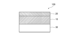
- FIG. 1 is a schematic cross-sectional view of the encapsulant of the present disclosure.
- FIG. 2 is a schematic cross-sectional view of the encapsulant of the present disclosure placed in contact with a compound having a non-stoichiometric composition.
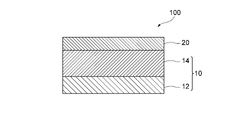
- FIG. 3 is a schematic cross-sectional view of an encapsulant having a first polymer layer, a second polymer layer, and an inorganic oxide insulator layer.
- FIG. 4 is a schematic cross-sectional view of a TFT manufactured in Examples.
- FIG. 5 is a schematic cross-sectional view of a TFT manufactured in Example.
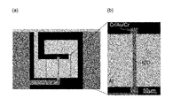
- FIG. 6 is an optical microscope photograph of a TFT produced in Example.
- FIG. 7 is a graph showing transmission characteristics of a TFT manufactured as a comparative example.
- FIG. 8 is a graph showing transmission characteristics of TFTs manufactured in Examples and Comparative Examples.
- FIG. 9 is a graph showing transmission characteristics of a TFT manufactured in Comparative Example before and after water treatment.
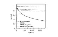
- FIG. 10 is a graph showing the measurement of the bias stress stability of the TFTs produced in Examples and Comparative Examples.
- FIG. 11 is a graph estimating the Vth shift value ( ⁇ Vth) by measuring the transfer characteristics before and after the bias stress of the TFTs manufactured in Examples and Comparative Examples.
- FIG. 12 is a graph showing measurement results of transfer characteristics of a TFT manufactured in a comparative example.
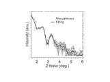
- FIG. 13 shows the film thickness evaluation results by X-ray reflectance measurement of the PMMA layer formed in Comparative Example.
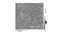
- FIG. 14 is an AFM measurement image of the IZO layer produced in Example.
- FIG. 15 is an AFM measurement image of the PMMA layer produced in Example.
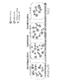
- FIG. 16 is a schematic diagram showing a method for preparing a precursor solution of amorphous metal oxide inorganic semiconductor (AOS) using a sol-gel method.
- FIG. 17 is a schematic diagram showing a method of forming an AOS layer using a spin coating method.
- FIG. 18 shows the measurement results of angle-resolved XPS of O1s.
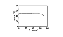
- FIG. 19 is a graph showing the angular dependence of the ratio ( ⁇ MOM ) of MOM (metal oxide state) to the entire O1s .
- FIG. 20 is a schematic diagram of an angle-resolved XPS measurement method.
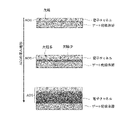
- FIG. 21 is a schematic cross-sectional view showing the distribution of the oxygen deficiency state depending on the thickness of the AOS film.
- FIG. 22 is a graph showing the thickness dependence of the ratio of each bond species to the total O1s from the substrate to the outermost surface of the AOS film.
- FIG. 23 is a graph showing evaluation of initial characteristics measured immediately after fabrication and characteristics after being left in the air for 20 months for the TFTs fabricated in Examples.
- the present disclosure is directed to an encapsulant for a compound having a non-stoichiometric composition comprising a polymer layer and an inorganic oxide insulator layer, the polymer layer comprising a first polymer layer comprising an organic solvent soluble polymer. do.
- an electronic device including a compound having a non-stoichiometric composition can stably operate for a long time under the atmosphere.
- the encapsulant of the present disclosure it is also possible to suppress damage to the compound having a non-stoichiometric composition due to the encapsulant arrangement process and the subsequent electronic element or electronic device manufacturing process. For example, after forming the encapsulant, even if another electronic element or electronic device is laminated and integrated on the encapsulant by a lithography process using water or an organic solvent, the deterioration of the compound having a non-stoichiometric composition can be suppressed.
- the encapsulants of the present disclosure enable the fabrication of complex integrated devices with compounds having non-stoichiometric compositions, such as complementary metal oxide semiconductors and inorganic/organic hybrid semiconductors.
- the encapsulants of the present disclosure can provide convenient and effective encapsulation, especially in printed electronics.
- FIG. 1 shows a schematic cross-sectional view of the sealing material 100 of the present disclosure.
- Encapsulant 100 includes polymer layer 10 and inorganic oxide insulator layer 20 .
- Polymer layer 10 comprises a first polymer layer comprising an organic solvent soluble polymer.
- Polymer layer 10 may consist of only the first polymer layer.
- the first polymer layer preferably consists of an organic solvent soluble polymer.
- Organic solvent soluble polymers refer to polymers that are soluble in organic solvents, including those that are polymers or oligomers when dissolved in organic solvents.
- the organic solvent is a solvent capable of dissolving the organic solvent-soluble polymer and not dissolving the compound having a non-stoichiometric composition, examples of which include butyl acetate, toluene, xylene, and acetonitrile.
- the first polymer layer containing an organic solvent-soluble polymer can be formed by a mild method called a solution process.
- the solution process does not utilize vacuum or radical reactions, thus avoiding the further formation of oxygen vacancies due to desorption of oxygen, and has the advantage of being very low or non-reactive with compounds having non-stoichiometric compositions. There is The solution process does not have reactions that generate acid. Therefore, the first polymer layer can be formed directly on a compound having a non-stoichiometric composition without substantially damaging it.
- FIG. 2 shows a cross-sectional schematic diagram when the sealing material 100 of the present disclosure is arranged so as to be in contact with the compound layer 30 having a non-stoichiometric composition.
- the polymer layer 10 of the sealing material 100 is located on the side of the compound layer 30 having a non-stoichiometric composition included in the electronic device, and the inorganic oxide insulator layer 20 is located on the side of the compound layer 30 having a non-stoichiometric composition.
- the encapsulant 100 can be used such that the .
- the polymer layer 10 of the encapsulant 100 is placed in contact with the compound layer 30 having a non-stoichiometric composition, but the polymer layer 10 of the encapsulant 100 and the compound having a non-stoichiometric composition Another layer may exist between the layer 30 and the polymer layer 10 of the encapsulant 100 and the compound layer 30 having a non-stoichiometric composition may not be in direct contact.
- the sealing material of the present disclosure is used as a sealing material for a thin film solar cell
- the compound layer having a non-stoichiometric composition is located inside the intermediate layer of the thin film solar cell, and the non-stoichiometric Other materials and electrodes may be laminated on the compound layer having the composition.
- the polymer layer 10 is present between the compound layer 30 having a non-stoichiometric composition and the inorganic oxide insulator layer 20 in this way, the non-stoichiometric composition when forming the inorganic oxide insulator layer 20 is reduced. It is possible to suppress damage to a compound having a theoretical composition.
- an inorganic oxide insulator layer such as an AlOx layer was formed directly on the material to be sealed and used as a sealing material.
- a compound having a non-stoichiometric composition such as IZOx prepared by a solution process using an atomic layer deposition (ALD) method
- ALD atomic layer deposition
- Chemical vapor deposition films such as parylene can be formed by chemical vapor deposition (CVD), which is relatively milder than ALD and does not require substrate heating.
- a chemical vapor deposition film of parylene or the like is also formed as an underlayer for forming the .
- CVD chemical vapor deposition
- a compound having a non-stoichiometric composition is highly sensitive to the environment, and is easily damaged by the vacuum environment and radicals generated during chemical vapor deposition film formation.
- a first polymer layer containing an organic solvent-soluble polymer on a compound having a non-stoichiometric composition by a solution process, the compound having a non-stoichiometric composition is substantially damaged.
- the polymer layer can be placed without giving.
- the first polymer layer can protect the compound with non-stoichiometric composition from the moisture associated with ALD methods or the vacuum environment of the sputtering process. Therefore, the inorganic oxide insulator layer can be formed on the polymer layer without substantially damaging the compound having a non-stoichiometric composition. Since the first polymer layer has a low density, it has low gas barrier performance and allows oxygen to permeate to some extent.
- the density of the first polymer layer is preferably 0.4-1.3 g/cm 3 , more preferably 0.5-1.2 g/cm 3 , still more preferably 0.6-1.1 g/cm 3 , More preferably, it is 0.7 to 1.0 g/cm 3 .
- the inorganic oxide insulator layer having a dense structure is positioned on the first polymer layer, moisture and oxygen are substantially impermeable through the encapsulant.
- the density of the first polymer layer is calculated from X-ray reflectometry. By fitting the X-ray reflectance data, the film thickness and film density can be simultaneously estimated as fitting parameters.
- Compounds having a non-stoichiometric composition include amorphous metal oxide inorganic semiconductors (AOS), metal chalcogenides, halide perovskites, and the like.
- AOS include ZnO, In 2 O 3 , In--Zn--O (IZO), In--Ga--Zn--O (IGZO), and especially AOS formed by a solution process.
- metal chalcogenides include layered substances such as molybdenum sulfide, tungsten sulfide and molybdenum selenide, and quantum dots such as lead sulfide and cadmium sulfide.
- halide perovskites include organic-inorganic hybrid substances represented by ABX 3 and A 2 BX 4 (A is an organic ammonium substance or an alkali metal, B is a metal such as lead or tin, and X is a halogen element), or an inorganic A metallic substance is mentioned.
- AOS layer can be confirmed to be amorphous by thin film X-ray diffraction.
- Examples of electronic devices comprising compounds having non-stoichiometric compositions include transistors, complementary metal oxide semiconductor devices, organic electroluminescence (organic EL), batteries, organic solar cells, oxide sensors, and the like.
- a transistor includes a thin film transistor, a field effect transistor, and the like.
- Oxide sensors also include chemical sensors, optical sensors, and the like. The same applies hereinafter.
- the sealing material of the present disclosure can have any shape, and can be a sealing film, a sealing sheet, or the like.
- the first polymer layer preferably has a thickness of 50 nm or more, more preferably 75 nm or more, and even more preferably 100 nm or more.
- the upper limit of the thickness of the first polymer layer is not particularly limited, but the thickness of the first polymer layer is preferably 1000 nm or less, more preferably 500 nm or less so as not to increase the thickness of the electronic device containing the encapsulant. Yes, 100 nm or less, 50 nm or less, or 30 nm or less.
- the polymer layer further includes a second polymer layer positioned between the first polymer layer and the inorganic oxide insulator layer, the second polymer layer being a chemical vapor deposition film.
- the preferred thickness of the first polymer layer may be as thin as 10 nm or greater.
- FIG. 3 shows a schematic cross-sectional view of the encapsulant 100 having the first polymer layer 12, the second polymer layer 14, and the inorganic oxide insulator layer 20.
- the encapsulant 100 includes a second polymer layer 14 located between the first polymer layer 12 and the inorganic oxide insulator layer 20 .
- a hybrid structure encapsulant 100 comprising a first polymer layer 12, a second polymer layer 14, and an inorganic oxide insulator layer 20
- the first polymer layer 12 comprising an organic solvent soluble polymer and chemical vapor deposition
- the second polymer layer 14 of the film acts as a buffer layer from damage by the ALD process or sputtering process when forming the inorganic oxide insulator layer 20, the inorganic oxide insulator layer 20 having a strong barrier effect.
- the chemical vapor deposition film is formed by a dry process, unlike the first polymer layer which is formed by a solution process. Therefore, since the second polymer layer is composed of a chemical vapor deposition film, it is dense and has a high barrier effect.
- the density of the second polymer layer, which is a chemical vapor deposition film, is higher than the density of the first polymer layer, which contains an organic solvent-soluble polymer.
- the density of the second polymer layer is preferably between 1.0 and 1.5 g/cm 3 , more preferably between greater than 1.0 and 1.45 g/cm 3 .
- the density of the second polymer layer is measured by ASTM D1505 or ASTM E1461.
- the thickness of the second polymer layer made of a chemical vapor deposition film is preferably 10-40 nm, more preferably 15-35 nm. Since the second polymer layer has a high density, a barrier effect can be obtained even within the above preferable thickness range, so that the overall thickness of the encapsulant can be reduced.
- the thickness of the inorganic oxide insulator layer is preferably 5 to 100 nm, more preferably 15 to 75 nm, still more preferably 25 to 55 nm. Since the inorganic oxide insulator layer has a higher barrier effect than the polymer layer, which is an organic film, it is possible to reduce the overall thickness of the sealing material while exhibiting a good barrier effect within the preferred thickness range. . Since the inorganic oxide insulator layer has a dense structure and is relatively hard, the thickness of the inorganic oxide insulator layer is preferably 100 nm or less from the viewpoint of ensuring the flexibility of the electronic element or electronic device including the sealing material. .
- the total thickness of the encapsulant is preferably is 100 nm or less, more preferably 90 nm or less, still more preferably 80 nm or less.
- the overall thickness of the encapsulant can be reduced if the second polymer layer is a chemical vapor deposition film.
- the lower limit of the thickness of the sealing material is preferably 25 nm or more, more preferably 40 nm or more.
- the organic solvent-soluble polymer is preferably an acrylic polymer, a styrenic polymer, a fluoropolymer, a thermally crosslinkable polymer, or a combination thereof.
- the acrylic polymer is preferably polymethyl methacrylate (PMMA), polyadamantyl methacrylate (PADMA), or polycyclohexyl methacrylate (PCMA).
- PMMA polymethyl methacrylate
- PADMA polyadamantyl methacrylate
- PCMA polycyclohexyl methacrylate
- the styrenic polymer is preferably polystyrene, poly- ⁇ -methylstyrene (P ⁇ MS), poly-4-methylstyrene (PMS), or polyvinylphenol (PVP).
- the fluoropolymer is preferably CYTOP (registered trademark) or Teflon (registered trademark) AF.
- the thermally crosslinkable polymer is preferably an epoxy resin or a thermosetting cycloolefin polymer.
- the inorganic oxide insulator of the inorganic oxide insulator layer is preferably AlOx, HfOx, ZrOx, SiOx, TiOx, or a combination thereof.
- x may be a value that satisfies the stoichiometric composition or a value that does not satisfy the stoichiometric composition. Since the inorganic oxide insulator layer has a high density and cannot penetrate large molecules such as water molecules and oxygen in the air, it has a high barrier effect against moisture and gas.
- the chemical vapor deposition film is preferably parylene.
- Parylene is preferable in terms of high denseness and uniformity because it is sequentially formed into a film at around room temperature. Parylene also includes its derivatives.
- the encapsulant preferably has a three-layer hybrid structure of a PMMA layer as a first polymer layer, a parylene layer as a second polymer layer, and an AlOx layer as an inorganic oxide insulator layer.
- a PMMA/Parylene/AlOx hybrid tri-layer encapsulation film can provide strong protection without degrading the performance of compounds with non-stoichiometric compositions.
- the compound having a non-stoichiometric composition is preferably an amorphous metal oxide inorganic semiconductor (AOS) film.
- AOS amorphous metal oxide inorganic semiconductor
- the AOS film preferably has a different distribution of oxygen vacancies in the direction perpendicular to the main surface of the AOS film, with more oxygen vacancies on the surface than on the inside.
- the distribution of the amount of oxygen defects in the thickness direction of the AOS layer was determined by angle-resolved X-ray photoelectron spectroscopy (XPS) as the ratio ( ⁇ M-O -M ) can be evaluated by measuring the angular dependence.
- XPS X-ray photoelectron spectroscopy
- An AOS layer having a distribution of the amount of oxygen defects in the thickness direction has fewer MOM (M: In or Zn) bonds closer to the outermost surface of the AOS layer.
- angle-resolved XPS is defined by the following formula 1 by changing the angle (tilt angle ⁇ ) with respect to the detector (analyzer) of XPS with the direction perpendicular to the surface of the measurement sample as the reference (0 °). and Equation 2: (where I 0 is the incident electron intensity, I (d) is the effective intensity at depth d from the surface, and ⁇ is the inelastic mean free path of the electron in the solid (estimated to be about 2.8 nm under the current measurement conditions).
- 3 ⁇ is the escape depth (I (d) ⁇ I 0 ⁇ 5%)) (where d is the depth from the surface, d inf is the detection depth (information depth), and ⁇ sub is the tilt angle of the substrate) from the surface of the film to be measured (information depth d inf ).
- the tilt angle ⁇ can be set in the range of 0° to less than 90°, preferably 0° to 70°.
- the ratio of ⁇ MOM on the outermost surface to ⁇ MOM in the interior is preferably 10% or more, more preferably 15% or more, and still more preferably 20% or more.
- the encapsulant of the present disclosure can be used for electronic devices.
- the encapsulating film of the present disclosure can be used as an encapsulant covering an electronic device containing a compound having a non-stoichiometric composition, preferably placed on a flexible substrate.
- Electronic devices including electronic elements include, for example, transistors, complementary metal oxide semiconductor devices, organic ELs, batteries, solar cells, oxide sensors and the like.
- the present disclosure also includes preparing a substrate, preparing an organic solvent in which a first polymer is dissolved, and coating the organic solvent in which the first polymer is dissolved on the substrate to form a first polymer layer. and forming an inorganic oxide insulator layer on the polymer layer using atomic layer deposition or sputtering to obtain a sealant
- the object is a method for producing a sealing material for a compound having
- an organic solvent in which the first polymer is dissolved is prepared.
- An organic solvent in which the first polymer is dissolved can be prepared by mixing the organic solvent and the first polymer.
- the concentration of the first polymer may vary depending on the desired thickness of the first polymer layer, eg, 1-80 mg/mL, 2-70 mg/mL, or 3-60 mg/mL.
- an organic solvent in which the first polymer is dissolved is applied onto the substrate to form a polymer layer including the first polymer layer.
- the coating method is preferably a spin coating method, a bar coating method, a spray coating method, a dip coating method, an inkjet method, a flexographic printing method, or a gravure printing method, more preferably a spin coating method, a bar coating method, or a spray coating method.
- the inorganic oxide insulator layer is formed using an atomic layer deposition (ALD) method or a sputtering method, preferably an atomic layer deposition (ALD) method.
- ALD atomic layer deposition
- the ALD method is preferable because it can form a film over a large area and can reduce costs.
- the film formation temperature of the inorganic oxide insulator layer is preferably 200°C or lower, more preferably 150°C or lower, and even more preferably 125°C or lower.
- the layers below the inorganic oxide insulator layer are less likely to be damaged.
- the flexible substrate is composed of an organic material such as polyethylene terephthalate (PET) or polyimide, it is possible to prevent the substrate from being damaged by forming the film within the preferable temperature range.
- forming the polymer layer comprises forming a second polymer layer that is a chemical vapor deposition film on the first polymer layer using chemical vapor deposition (CVD), wherein the inorganic Forming an oxide insulator layer includes forming an inorganic oxide insulator layer over the second polymer layer.
- CVD chemical vapor deposition
- the second polymer layer which is a chemical vapor deposition film, is deposited by CVD.
- CVD is a light vacuum process, and is preferred in terms of deposition rate, processing area, denseness, and uniformity.
- the contents regarding the sealing material described above are applied.
- Example 1 (Fabrication of TFT with two-layer encapsulant and IZO) (Preparation of AOS precursor solution by sol-gel method)
- a precursor solution of indium zinc oxide (IZO) was prepared by the sol-gel method schematically shown in FIG. 0.462 g of In(NO 3 ) 3 -xH 2 O (Aldrich) was added to 10 mL of 2-methoxyethanol and stirred under air for 6 hours to obtain an indium precursor solution (0.1 M). .
- 0.297 g of Zn(NO 3 ) 2 -xH 2 O (Aldrich) was added to 10 mL of 2-methoxyethanol and stirred under air for 6 hours to obtain a zinc precursor solution (0.1 M).
- a P-doped Si wafer substrate having thermally oxidized SiO 2 (100 nm thick) as a gate insulating film was ultrasonically cleaned in acetone and then in 2-propanol for 10 minutes each, then using a hot plate at 100° C. for 10 minutes in the atmosphere. dried.
- the prepared IZO precursor solution was spin-coated onto the UV-treated substrate at 500 rpm for 5 seconds and then at 5000 rpm for 30 seconds to form an IZO intermediate film.
- the formed IZO intermediate film was subjected to heat treatment at 150° C. for 5 minutes in an air atmosphere, and further heat treatment at 370° C. for 1 hour to form an AOS film (IZO film) having a thickness of 6 nm.
- Source/drain (S/D) electrodes Al, 40 nm were formed and patterned on the IZO film by thermal evaporation using a metal mask. Further, the IZO film was patterned with an yttrium aluminum garnet (YAG) laser, heat-treated at 90° C. for 3 hours in the atmosphere, and slowly cooled to room temperature to obtain an IZO active layer.
- YAG yttrium aluminum garnet
- a butyl acetate solution (50 mg/mL) in which PMMA (Mw: 120,000) is dissolved is spin-coated at 500 rpm for 5 seconds and at 4000 rpm for 30 seconds on the gate insulating layer on which the IZO active layer and S/D electrodes are formed.
- heat treatment was performed at 150° C. for 2 hours to form a PMMA layer with a thickness of 100 nm.
- AlOx having a thickness of 40 nm was deposited on the PMMA layer using the ALD method while maintaining the substrate temperature at 110° C. to form a two-layer sealing film of PMMA layer/AlOx layer. In this manner, a bottom-gate/top-contact TFT having a sealing material and an IZO film was produced.
- FIG. 4 shows a schematic cross-sectional view of the fabricated TFT.
- the fabricated TFT had a channel length (L) of 100 ⁇ m and a channel width (W) of 2000 ⁇ m.
- Example 2 Fabrication of TFT with 3-layer encapsulant and IZO
- An IZO precursor solution was prepared under the same conditions as in Example 1.
- Cr/Au/Cr is vapor-deposited on a pattern formed with a photoresist (TLOR, Tokyo Ohka Kogyo Co., Ltd.), and then by a lift-off method of removing the photoresist, Cr having a thickness of 5/25/5 nm is deposited.
- /Au/Cr gate electrodes were formed.
- An AlOx gate insulating film with a thickness of 75 nm was formed using the ALD method.
- an IZO film was formed under the same conditions as in Example 1.
- the formed IZO film was subjected to photolithography using a photosensitive dielectric (PDM, Taiyo Ink Mfg. Co., Ltd.) and wet etching with a 1.75% by mass oxalic acid aqueous solution to obtain a patterned n-type IZO active semiconductor. formed a layer.
- PDM photosensitive dielectric
- photolithography was performed using a photosensitive dielectric (PDM, Taiyo Ink Mfg. Co., Ltd.) and used as a shadow mask to form source/drain S/D electrodes with a thickness of 60 nm by Al thermal evaporation and lift-off.
- PDM photosensitive dielectric
- the laminate with the S/D electrodes formed thereon was heat-treated in the air at 90° C. for 3 hours, and slowly cooled to room temperature.
- a butyl acetate solution (5 mg/mL) in which PMMA (Mw: 120,000) is dissolved is spin-coated at 500 rpm for 5 seconds and at 4000 rpm for 30 seconds on the gate insulating layer on which the IZO active layer and S/D electrodes are formed. After that, heat treatment was performed at 150° C. for 1 hour to form a PMMA layer with a thickness of 13 nm.
- a parylene layer with a thickness of 25 nm was deposited on the PMMA layer using the CVD method.
- AlOx having a thickness of 40 nm was deposited on the parylene layer by ALD while the substrate temperature was maintained at 110° C. to form a three-layer sealing film of PMMA layer/parylene layer/AlOx layer. In this manner, a bottom-gate/top-contact TFT having a sealing material and an IZO film was produced.
- FIG. 5 shows a schematic cross-sectional view of the fabricated TFT.
- FIG. 6 is an optical micrograph of the fabricated TFT. The fabricated TFT had a channel length (L) of 10 ⁇ m and a channel width (W) of 200 ⁇ m.
- FIG. 6(a) is an optical microscope photograph of the manufactured TFT observed from above, and FIG. 6(b) is an enlarged photograph of the portion surrounded by a square in FIG. 6(a).
- Example 1 A TFT was fabricated in the same manner as in Example 2, except that the sealing film was a PMMA single layer with a thickness of 13 nm.
- Example 2 A TFT was fabricated in the same manner as in Example 2, except that the sealing film was a parylene single layer having a thickness of 25 nm.
- Example 3 A TFT was fabricated in the same manner as in Example 2, except that the sealing film was an AlOx single layer with a thickness of 40 nm.
- Example 5 A TFT was fabricated in the same manner as in Example 2, except that the sealing film was a PMMA layer with a thickness of 13 nm and a parylene layer with a thickness of 25 nm disposed thereon.
- the TFTs fabricated in Examples and Comparative Examples were electrically measured under normal temperature and dark conditions.
- the surface roughness was measured using an atomic force microscope (AFM, SPM-9700HT manufactured by Shimadzu Corporation).
- a YAG laser was used to form a through hole in the sealing material, and a silver paste was used to ensure conduction.
- FIG. 7 shows the TFTs containing the encapsulant of Comparative Example 1 (PMMA single layer), Comparative Example 2 (Parylene single layer), Comparative Example 3 (AlOx single layer), and the TFT containing no encapsulant of Comparative Example 4. shows the measurement results of the transfer characteristics of
- the TFT of Comparative Example 4 (without encapsulant) had a saturation mobility ( ⁇ sat ) of 2.3 cm 2 V ⁇ 1 s ⁇ 1 , an on/off current ratio (I on /I off ) of about 10 8 , and The threshold voltage (Vth) was 2.0V. This value serves as a reference value for comparison.
- the TFT of Comparative Example 1 (PMMA single layer) has desirable properties such as ⁇ sat of 2.0 cm 2 V ⁇ 1 s ⁇ 1 , I on /I off ⁇ 10 8 , Vth of 1.7 V, and negligible hysteresis. showed that.
- the TFT of Comparative Example 2 (single layer of parylene) had a large Vth shift to the negative side. This is because the long vacuum conditions during parylene deposition and the reactive radical species originating from the parylene source, which may react with weakly bonded oxygen atoms, affected the IZO active layer with a non-stoichiometric composition. Conceivable.
- the TFT of Comparative Example 3 (AlOx single layer) had a large Vth shift to the negative side.
- the performance was even lower than that of the TFT of Comparative Example 2 (single layer of parylene). This is believed to be due to the harsh conditions of the ALD process, such as high vacuum, high temperature (110° C.), and use of water as a reactive species.
- the parylene coating process and ALD method changed the properties of the IZO active layer with non-stoichiometric composition.
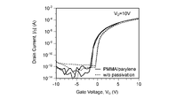
- FIG. 8 shows the measurement results of the transfer characteristics of the TFT containing the sealing material of Example 2 (three layers of PMMA layer/Parylene layer/AlOx layer) and the TFT containing no sealing material of Comparative Example 4.
- FIG. 8 shows the measurement results of the transfer characteristics of the TFT containing the sealing material of Example 2 (three layers of PMMA layer/Parylene layer/AlOx layer) and the TFT containing no sealing material of Comparative Example 4.
- the TFT of Example 2 Compared with the TFT of Comparative Example 4, the TFT of Example 2 exhibited substantially the same characteristics. That is, it was confirmed that the two layers of the PMMA layer/parylene layer functioned as protective layers during the AlOx film formation by the ALD method.
- the TFT of Comparative Example 1 (PMMA single layer), the TFT of Comparative Example 4 (no encapsulant), and the TFT of Comparative Example 5 (PMMA/Parylene bilayer) were immersed in deionized water for 15 minutes and air-dried. (hereinafter referred to as water treatment).
- the transfer characteristics of each water-treated TFT were measured to evaluate the waterproof characteristics.
- the characteristics of the TFT of Comparative Example 4 (without encapsulant) before water treatment were used as a reference for evaluation.
- FIG. 9 shows the characteristics of the TFT of Comparative Example 4 (no encapsulant) before and after water treatment, and the TFTs of Comparative Example 1 (PMMA single layer) and Comparative Example 5 (PMMA/parylene double layer) after water treatment. later characteristics.
- the TFT of Comparative Example 1 (PMMA single layer) showed a slight Vth shift, but the hysteresis was negligible.
- the TFT of Comparative Example 5 (PMMA/Parylene bilayer) exhibited substantially the same characteristics as the TFT of Comparative Example 4 (no encapsulant) prior to water treatment. That is, it is shown that the PMMA/parylene bilayer has a strong ability to protect against moisture, and it can be seen that it also has a protective ability in the film formation process by the ALD method. Due to the low moisture permeability of parylene, the PMMA/parylene bilayer has a better buffer function than the PMMA single layer during AlOx deposition.
- TFT of Example 2 (three layers of PMMA layer/Parylene layer/AlOx layer), TFT of Comparative Example 1 (PMMA single layer), TFT of Comparative Example 4 (without sealing material), and TFT of Comparative Example 5 (PMMA/Parylene Bilayer) TFT was evaluated for bias stress stability at room temperature (25° C.).
- FIG. 10 shows the measurement results of the bias stress stability.
- the bias stress stability was evaluated by measuring the drain current (I D ) throughout the process and calculating the I D decrease rate after 3700 seconds defined by the following equation 3.
- I D (0) is the initial drain current and I D (t) is I D after bias stress at each time (t).
- the TFT of Comparative Example 4 (with no encapsulant) had an ID reduction rate of 67% and had the worst stability of bias stress.
- the ID reduction rate of the TFT of Comparative Example 1 ( PMMA single layer) was suppressed to 21%, and the ID reduction rate of the TFT of Comparative Example 5 (PMMA/parylene double layer) was suppressed to 17%.
- the ID reduction rate was greatly suppressed, and the ID reduction rate was 2%.
- FIG. 11 shows the measurement results of the transfer characteristics before and after the bias stress.
- ⁇ Vth of the TFT of Comparative Example 4 was 2.8V.
- ⁇ Vth of the TFT of Comparative Example 1 PMMA single layer
- ⁇ Vth of the TFT of Comparative Example 5 PMMA/parylene two layers
- ⁇ Vth was suppressed to 0.2V in the TFT of Example 2 (three layers of PMMA layer/parylene layer/AlOx layer). This is because the IZO active layer was not damaged due to the barrier effect of the PMMA/parylene buffer layer when AlOx was deposited by the ALD method.
- FIG. 12 shows the measurement results of the transfer characteristics of the TFT containing the sealing material of Comparative Example 5 (PMMA/parylene bilayer) and the TFT containing no sealing material of Comparative Example 4.
- FIG. 12 shows the measurement results of the transfer characteristics of the TFT containing the sealing material of Comparative Example 5 (PMMA/parylene bilayer) and the TFT containing no sealing material of Comparative Example 4.
- FIG. 13 shows the X-ray reflectance measurement results of the PMMA layer formed under the same conditions as in Comparative Example 5. As shown in FIG. It can be seen that although the thickness of the PMMA layer is only 13 nm, the IZO active layer with non-stoichiometric composition can be effectively protected from radicals during parylene deposition.
- FIG. 14 shows an AFM measurement image of the IZO layer produced under the same conditions as in Example 1.
- FIG. 15 shows an AFM measurement image of the PMMA layer formed on the IZO layer produced under the same conditions as in Example 1.
- the IZO layer had a surface roughness RMS of 0.196 nm, and the PMMA layer formed on the IZO layer had a flat, pinhole-free structure with a surface roughness RMS of 0.334 nm.
- FIG. 18 shows the measurement results of the O1s angle-resolved XPS of the AOS layer (IZO film) produced by the same method as in Example 1.
- FIG. 18A is a graph summarizing measured spectra of O1s of the AOS layer when the tilt angles ⁇ are 0°, 40°, 55°, 63°, and 70°.
- FIGS. 18(b) to 18(f) show measurement spectra measured at tilt angles ⁇ of 0°, 40°, 55°, 63°, and 70°.
- -OM, MO(H) with a peak at 531.1 eV, and MO(H) with a peak at 532.0 eV are decomposed and fitted graphs.
- M means In or Zn.
- MOM means oxygen bridging between metal centers and means a stoichiometric oxide with no oxygen defects.
- MO(H) means an oxygen or hydroxyl group having an unpaired electron that does not bridge between metal centers, and MOR is an organic substance such as H 2 O, CO 2 , or alcohol bound to the metal center. of oxygen, and each means a composition with oxygen vacancies.
- the ratio of MOM bonds is constant at about 50% in the interior of the AOS film, but the closer to the surface of the AOS film, the lower the ratio of MOM bonds, down to about 40%.
- the proportion of -OM bonds was reduced by about 20%.
- the three points at 5.5 nm on the horizontal axis are the ratios of the integrated values of each MO species from the top surface of AOS to the depth of 5.5 nm, and the three points at 2.8 nm are from the top surface. It is the percentage of integrated values of MO species up to a depth of 2.8 nm.
Landscapes
- Chemical & Material Sciences (AREA)
- Engineering & Computer Science (AREA)
- Chemical Kinetics & Catalysis (AREA)
- Mechanical Engineering (AREA)
- General Chemical & Material Sciences (AREA)
- Materials Engineering (AREA)
- Metallurgy (AREA)
- Organic Chemistry (AREA)
- Inorganic Chemistry (AREA)
- Formation Of Insulating Films (AREA)
- Ceramic Engineering (AREA)
- Physics & Mathematics (AREA)
- Optics & Photonics (AREA)
- Sealing Material Composition (AREA)
- Electroluminescent Light Sources (AREA)
Abstract
Description
(1)ポリマー層及び無機酸化物絶縁体層を含み、
前記ポリマー層は、有機溶媒可溶性ポリマーを含む第1のポリマー層を含む、
非化学量論組成を有する化合物用封止材。
(2)前記ポリマー層は、前記第1のポリマー層と前記無機酸化物絶縁体層との間に位置する第2のポリマー層をさらに含み、
前記第2のポリマー層は、化学気相成長膜からなる、
上記(1)に記載の封止材。
(3)前記第1のポリマー層、前記第2のポリマー層、及び前記無機酸化物絶縁体層の合計厚みが100nm以下である、上記(2)に記載の封止材。
(4)前記有機溶媒可溶性ポリマーは、アクリル系ポリマー、スチレン系ポリマー、フッ素系ポリマー、熱架橋性ポリマー、またはそれらの組み合わせである、上記(1)~(3)のいずれかに記載の封止材。
(5)前記無機酸化物絶縁体層の無機酸化物絶縁体が、AlOx、HfOx、ZrOx、SiOx、TiOx、またはそれらの組み合わせである、上記(1)~(4)のいずれかに記載の封止材。
(6)前記化学気相成長膜がパリレンである、上記(2)~(5)のいずれかに記載の封止材。
(7)前記非化学量論組成を有する化合物が、アモルファス金属酸化物無機半導体膜である、上記(1)~(6)のいずれかに記載の封止材。
(8)前記アモルファス金属酸化物無機半導体膜が、前記膜の主表面に垂直方向に酸素欠損状態が異なる分布を有し、表面が内部よりも酸素欠損が多い、上記(7)に記載の封止材。
(9)上記(1)~(8)のいずれかに記載の封止材を含む電子素子。
(10)基板を準備すること、
第1のポリマーが溶解した有機溶媒を調製すること、
前記基板上に、前記第1のポリマーが溶解した有機溶媒を塗布して第1のポリマー層を含むポリマー層を形成すること、及び
前記ポリマー層上に、原子層堆積法またはスパッタリング法を用いて無機酸化物絶縁体層を形成して、封止材を得ること
を含む、非化学量論組成を有する化合物用封止材の製造方法。
(11)前記ポリマー層を形成することが、前記第1のポリマー層上に、化学気相成長法を用いて化学気相成長膜である第2のポリマー層を形成することを含み、
前記無機酸化物絶縁体層を形成することが、前記第2のポリマー層上に前記無機酸化物絶縁体層を形成することを含む、
上記(10)に記載の封止材の製造方法。


(2層封止材及びIZOを備えたTFTの作製)
(ゾルゲル法によるAOS前駆体溶液の調製)
図16に模式的に示すゾルゲル法で酸化インジウム亜鉛(IZO)の前駆体溶液を調製した。10mLの2-メトキシエタノールに0.462gのIn(NO3)3-xH2O(Aldrich)を添加し、大気下で6時間撹拌して、インジウムの前駆体溶液(0.1M)を得た。10mLの2-メトキシエタノールに0.297gのZn(NO3)2-xH2O(Aldrich)を添加し、大気下で6時間撹拌して、亜鉛の前駆体溶液(0.1M)を得た。得られたインジウム及び亜鉛の前駆体溶液を、In:Zn=3:2のモル比で混合し、大気下で6時間撹拌して、IZOの前駆体溶液を調製した。
上記洗浄及び乾燥した基板をUVオゾンクリーナー(フィルゲン社製、UV253H)で10分間処理し、有機残渣を除去し、濡れ性を向上させた。
IZO活性層及びS/D電極を形成したゲート絶縁層上に、PMMA(Mw:120,000)を溶解させた酢酸ブチル溶液(50mg/mL)を、500rpmで5秒間、4000rpmで30秒間スピンコートした後、150℃で2時間熱処理を行い、厚みが100nmのPMMA層を形成した。PMMA層上に、ALD法を用いて、基板温度を110℃に保ちながら、厚みが40nmのAlOxを堆積させて、PMMA層/AlOx層の2層の封止膜を形成した。このようにして、封止材とIZO膜とを有するボトムゲート・トップコンタクトTFTを作製した。
(3層封止材及びIZOを備えたTFTの作製)
実施例1と同じ条件でIZO前駆体溶液を調製した。ガラス基板上に、フォトレジスト(TLOR、東京応化工業株式会社)で形成したパターン上にCr/Au/Crを蒸着し、次いでフォトレジストを除去するリフトオフ法により、厚みが5/25/5nmのCr/Au/Crのゲート電極を形成した。ALD法を用いて、厚みが75nmのAlOxゲート絶縁膜を形成した。
封止膜を、厚みが13nmのPMMA単層にしたこと以外は、実施例2と同様に、TFTを作製した。
封止膜を、厚みが25nmのパリレン単層にしたこと以外は、実施例2と同様に、TFTを作製した。
封止膜を、厚みが40nmのAlOx単層にしたこと以外は、実施例2と同様に、TFTを作製した。
封止膜を形成しなかったこと以外は、実施例2と同様に、TFTを作製した。
封止膜を、厚みが13nmのPMMA層及びその上に配置した厚みが25nmのパリレン層にしたこと以外は、実施例2と同様に、TFTを作製した。
比較例1~4で作製したTFTの伝達特性を測定し、TFT作製プロセスによる活性層の性能への影響を評価した。
図8に、実施例2(PMMA層/パリレン層/AlOx層の3層)の封止材を含むTFT、及び比較例4の封止材を含まないTFTの伝達特性の測定結果を示す。
比較例1(PMMA単層)のTFT、比較例4(封止材無し)のTFT、及び比較例5(PMMA/パリレンの2層)のTFTを、脱イオン水に15分間浸漬して風乾させた(以下、水処理という)。水処理した各TFTの伝達特性を測定して、防水特性を評価した。比較例4(封止材無し)のTFTの水処理前の特性を基準にして、評価した。
実施例2(PMMA層/パリレン層/AlOx層の3層)のTFT、比較例1(PMMA単層)のTFT、比較例4(封止材無し)のTFT、及び比較例5(PMMA/パリレン2層)のTFTについて、室温(25℃)でのバイアス応力安定性を評価した。図10に、バイアス応力安定性の測定結果を示す。

O2(g)+e-(s)=2O-(s)
で表されるように、吸収した酸素が導電性ボンドから電子を奪い取ることができたためと考えられる。
実施例2(PMMA層/パリレン層/AlOx層の3層)のTFT、比較例1(PMMA単層)のTFT、比較例4(封止材無し)のTFT、及び比較例5(PMMA/パリレン2層)のTFTについて、バイアス応力の前後で伝達特性を測定して、Vthシフト値(ΔVth)を見積もった。図11に、バイアス応力の前後で伝達特性の測定結果を示す。
図12に、比較例5(PMMA/パリレン2層)の封止材を含むTFT、及び比較例4の封止材を含まないTFTの伝達特性の測定結果を示す。
図18に、実施例1と同様の方法で作製したAOS層(IZO膜)のO1sの角度分解XPSの測定結果を示す。図18(a)は、傾斜角θを0°、40°、55°、63°、及び70°としたときの、AOS層のO1sの測定スペクトルをまとめたグラフである。図18(b)~図18(f)は、傾斜角θを0°、40°、55°、63°、及び70°として測定した測定スペクトルを、結合エネルギーが529.7eVにピークを持つM-O-M、531.1eVにピークを持つM-O(H)、及び532.0eVにピークを持つM-O-Rに分解及びフィッティングしたグラフである。
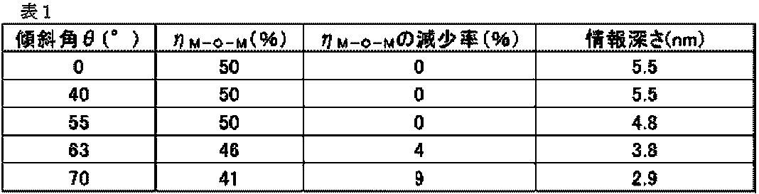
図23に、実施例2で作製したW/L=200μm/10μmのTFTデバイスを、作製直後に測定した初期特性及び大気中に20ヶ月放置後の特性を評価したグラフを示す。20ヶ月放置後において若干の変化がみられたが、初期特性及び20ヶ月放置後において、実質的に同じ特性を示し、良好な長期安定性を有することが分かった。
10 ポリマー層
12 第1のポリマー層
14 第2のポリマー層
20 無機酸化物絶縁体層
30 非化学量論組成を有する化合物層
Claims (11)
- ポリマー層及び無機酸化物絶縁体層を含み、
前記ポリマー層は、有機溶媒可溶性ポリマーを含む第1のポリマー層を含む、
非化学量論組成を有する化合物用封止材。 - 前記ポリマー層は、前記第1のポリマー層と前記無機酸化物絶縁体層との間に位置する第2のポリマー層をさらに含み、
前記第2のポリマー層は、化学気相成長膜からなる、
請求項1に記載の封止材。 - 前記第1のポリマー層、前記第2のポリマー層、及び前記無機酸化物絶縁体層の合計厚みが100nm以下である、請求項2に記載の封止材。
- 前記有機溶媒可溶性ポリマーは、アクリル系ポリマー、スチレン系ポリマー、フッ素系ポリマー、熱架橋性ポリマー、またはそれらの組み合わせである、請求項1~3のいずれか一項に記載の封止材。
- 前記無機酸化物絶縁体層の無機酸化物絶縁体が、AlOx、HfOx、ZrOx、SiOx、TiOx、またはそれらの組み合わせである、請求項1~4のいずれか一項に記載の封止材。
- 前記化学気相成長膜がパリレンである、請求項2~5のいずれか一項に記載の封止材。
- 前記非化学量論組成を有する化合物が、アモルファス金属酸化物無機半導体膜である、請求項1~6のいずれか一項に記載の封止材。
- 前記アモルファス金属酸化物無機半導体膜が、前記膜の主表面に垂直方向に酸素欠損状態が異なる分布を有し、表面が内部よりも酸素欠損が多い、請求項7に記載の封止材。
- 請求項1~8のいずれか一項に記載の封止材を含む電子素子。
- 基板を準備すること、
第1のポリマーが溶解した有機溶媒を調製すること、
前記基板上に、前記第1のポリマーが溶解した有機溶媒を塗布して第1のポリマー層を含むポリマー層を形成すること、及び
前記ポリマー層上に、原子層堆積法またはスパッタリング法を用いて無機酸化物絶縁体層を形成して、封止材を得ること
を含む、非化学量論組成を有する化合物用封止材の製造方法。 - 前記ポリマー層を形成することが、前記第1のポリマー層上に、化学気相成長法を用いて化学気相成長膜である第2のポリマー層を形成することを含み、
前記無機酸化物絶縁体層を形成することが、前記第2のポリマー層上に前記無機酸化物絶縁体層を形成することを含む、
請求項10に記載の封止材の製造方法。
Priority Applications (4)
| Application Number | Priority Date | Filing Date | Title |
|---|---|---|---|
| KR1020237032186A KR102882953B1 (ko) | 2021-02-25 | 2022-02-24 | 비화학양론 조성을 갖는 화합물용 봉지재 및 그 제조 방법 |
| EP22759741.6A EP4300548A4 (en) | 2021-02-25 | 2022-02-24 | ENCAPSULATING AGENT FOR A COMPOUND HAVING A NON-STOICHIOMETRICAL COMPOSITION AND METHOD FOR THE PRODUCTION THEREOF |
| CN202280016616.0A CN116941019A (zh) | 2021-02-25 | 2022-02-24 | 具有非化学计量组成的化合物用密封件及其制造方法 |
| US18/277,129 US20240128144A1 (en) | 2021-02-25 | 2022-02-24 | Sealing material for compounds having non-stoichiometric composition and method for manufacturing same |
Applications Claiming Priority (2)
| Application Number | Priority Date | Filing Date | Title |
|---|---|---|---|
| JP2021-029328 | 2021-02-25 | ||
| JP2021029328A JP7637942B2 (ja) | 2021-02-25 | 2021-02-25 | 非化学量論組成を有する化合物用封止材及びその製造方法 |
Publications (1)
| Publication Number | Publication Date |
|---|---|
| WO2022181706A1 true WO2022181706A1 (ja) | 2022-09-01 |
Family
ID=83049144
Family Applications (1)
| Application Number | Title | Priority Date | Filing Date |
|---|---|---|---|
| PCT/JP2022/007657 Ceased WO2022181706A1 (ja) | 2021-02-25 | 2022-02-24 | 非化学量論組成を有する化合物用封止材及びその製造方法 |
Country Status (6)
| Country | Link |
|---|---|
| US (1) | US20240128144A1 (ja) |
| EP (1) | EP4300548A4 (ja) |
| JP (1) | JP7637942B2 (ja) |
| KR (1) | KR102882953B1 (ja) |
| CN (1) | CN116941019A (ja) |
| WO (1) | WO2022181706A1 (ja) |
Families Citing this family (1)
| Publication number | Priority date | Publication date | Assignee | Title |
|---|---|---|---|---|
| DE102023004582A1 (de) * | 2023-11-13 | 2025-05-15 | Mercedes-Benz Group AG | Orts- und kontextbasierte automobile Videospiel-Plattform |
Citations (3)
| Publication number | Priority date | Publication date | Assignee | Title |
|---|---|---|---|---|
| WO2007094361A1 (ja) * | 2006-02-16 | 2007-08-23 | Idemitsu Kosan Co., Ltd. | 有機薄膜トランジスタ及び有機薄膜発光トランジスタ |
| JP2010093172A (ja) * | 2008-10-10 | 2010-04-22 | Fujifilm Corp | 封止デバイス |
| JP2011086923A (ja) * | 2009-09-16 | 2011-04-28 | Semiconductor Energy Lab Co Ltd | トランジスタ及び表示装置 |
Family Cites Families (5)
| Publication number | Priority date | Publication date | Assignee | Title |
|---|---|---|---|---|
| US8173906B2 (en) * | 2007-02-07 | 2012-05-08 | Raytheon Company | Environmental protection coating system and method |
| KR100926030B1 (ko) * | 2008-02-25 | 2009-11-11 | 한국과학기술연구원 | 산소와 수분 투과의 차단 및 가스 배리어 특성 향상을 위한유/무기 복합 박막 보호층 및 그의 제조방법 |
| KR101688739B1 (ko) * | 2015-07-30 | 2016-12-23 | 연세대학교 산학협력단 | 침습형 생체소자 제조방법 및 그 생체소자 |
| JP6561366B2 (ja) * | 2016-03-16 | 2019-08-21 | 株式会社Joled | 半導体装置とその製造方法 |
| US11139164B2 (en) * | 2019-12-12 | 2021-10-05 | Raytheon Company | Electronic device including hermetic micro-cavity and methods of preparing the same |
-
2021
- 2021-02-25 JP JP2021029328A patent/JP7637942B2/ja active Active
-
2022
- 2022-02-24 KR KR1020237032186A patent/KR102882953B1/ko active Active
- 2022-02-24 EP EP22759741.6A patent/EP4300548A4/en active Pending
- 2022-02-24 US US18/277,129 patent/US20240128144A1/en active Pending
- 2022-02-24 WO PCT/JP2022/007657 patent/WO2022181706A1/ja not_active Ceased
- 2022-02-24 CN CN202280016616.0A patent/CN116941019A/zh active Pending
Patent Citations (3)
| Publication number | Priority date | Publication date | Assignee | Title |
|---|---|---|---|---|
| WO2007094361A1 (ja) * | 2006-02-16 | 2007-08-23 | Idemitsu Kosan Co., Ltd. | 有機薄膜トランジスタ及び有機薄膜発光トランジスタ |
| JP2010093172A (ja) * | 2008-10-10 | 2010-04-22 | Fujifilm Corp | 封止デバイス |
| JP2011086923A (ja) * | 2009-09-16 | 2011-04-28 | Semiconductor Energy Lab Co Ltd | トランジスタ及び表示装置 |
Non-Patent Citations (2)
| Title |
|---|
| S. ZHAN ET AL., PHYS. STATUS SOLIDUS, vol. 217, 2020, pages 1900832 |
| See also references of EP4300548A4 |
Also Published As
| Publication number | Publication date |
|---|---|
| US20240128144A1 (en) | 2024-04-18 |
| EP4300548A1 (en) | 2024-01-03 |
| KR20230148221A (ko) | 2023-10-24 |
| JP2022130244A (ja) | 2022-09-06 |
| EP4300548A4 (en) | 2024-08-14 |
| CN116941019A (zh) | 2023-10-24 |
| JP7637942B2 (ja) | 2025-03-03 |
| KR102882953B1 (ko) | 2025-11-10 |
| TW202235280A (zh) | 2022-09-16 |
Similar Documents
| Publication | Publication Date | Title |
|---|---|---|
| Lee et al. | Inkjet printed high-mobility indium zinc tin oxide thin film transistors | |
| US7507618B2 (en) | Method for making electronic devices using metal oxide nanoparticles | |
| Seon et al. | Spin-coated CdS thin films for n-channel thin film transistors | |
| KR102060492B1 (ko) | 고성능 및 전기 안정성의 반전도성 금속 산화물 층의 제조 방법, 및 상기 방법에 따라 제조된 층 및 그의 용도 | |
| JP6180908B2 (ja) | 金属酸化物半導体膜、薄膜トランジスタ、表示装置、イメージセンサ及びx線センサ | |
| JP2017503336A (ja) | 低接触抵抗薄膜トランジスタ | |
| CN102379042B (zh) | 场效应晶体管、其制造方法以及使用了该场效应晶体管的电子器件 | |
| CN107408510B (zh) | 薄膜晶体管、薄膜晶体管的制造方法及使用了薄膜晶体管的图像显示装置 | |
| Li et al. | Broadband phototransistors realised by incorporating a bi-layer perovskite/NIR light absorbing polymer channel | |
| Li et al. | Precise Patterning of Large‐Scale TFT Arrays Based on Solution‐Processed Oxide Semiconductors: A Comparative Study of Additive and Subtractive Approaches | |
| JP5200322B2 (ja) | 半導体デバイスおよびその製造方法 | |
| Le et al. | Bulk charge-transfer doping of amorphous metal oxide: fullerene blends for solution-processed amorphous indium zinc oxide thin-film transistors | |
| KR100960808B1 (ko) | 산화물 반도체 박막 및 그 제조 방법 | |
| Wu et al. | Ultraviolet light sensitive In‐doped ZnO thin film field effect transistor printed by inkjet technique | |
| JP2007150156A (ja) | トランジスタおよびその製造方法 | |
| KR102882953B1 (ko) | 비화학양론 조성을 갖는 화합물용 봉지재 및 그 제조 방법 | |
| Lee et al. | Inkjet-printed oxide thin-film transistors using double-active layer structure | |
| JP2011077450A (ja) | 薄膜トランジスタ及び薄膜トランジスタの製造方法 | |
| TWI918865B (zh) | 具有非化學計量組成之化合物用密封材及其製造方法 | |
| US20130277661A1 (en) | Field-effect transistor, process for producing the same, and electronic device including the same | |
| JP5870502B2 (ja) | 有機半導体素子およびその製造方法 | |
| Kato et al. | Effects of Potassium Doping on the Active Layer of Inverse-Structured Perovskite Solar Cells | |
| JP6177713B2 (ja) | 薄膜の製造方法 | |
| KR102764160B1 (ko) | 무기/유기 하이브리드 상보형 반도체 디바이스 및 그 제조 방법 | |
| JP2013038194A (ja) | 有機トランジスタ及びその製造方法 |
Legal Events
| Date | Code | Title | Description |
|---|---|---|---|
| 121 | Ep: the epo has been informed by wipo that ep was designated in this application |
Ref document number: 22759741 Country of ref document: EP Kind code of ref document: A1 |
|
| WWE | Wipo information: entry into national phase |
Ref document number: 18277129 Country of ref document: US |
|
| WWE | Wipo information: entry into national phase |
Ref document number: 202280016616.0 Country of ref document: CN |
|
| ENP | Entry into the national phase |
Ref document number: 20237032186 Country of ref document: KR Kind code of ref document: A |
|
| WWE | Wipo information: entry into national phase |
Ref document number: 1020237032186 Country of ref document: KR |
|
| WWE | Wipo information: entry into national phase |
Ref document number: 2022759741 Country of ref document: EP |
|
| NENP | Non-entry into the national phase |
Ref country code: DE |
|
| ENP | Entry into the national phase |
Ref document number: 2022759741 Country of ref document: EP Effective date: 20230925 |