WO2022182018A1 - 카메라 모듈 및 이를 포함하는 전자 장치 - Google Patents
카메라 모듈 및 이를 포함하는 전자 장치 Download PDFInfo
- Publication number
- WO2022182018A1 WO2022182018A1 PCT/KR2022/001969 KR2022001969W WO2022182018A1 WO 2022182018 A1 WO2022182018 A1 WO 2022182018A1 KR 2022001969 W KR2022001969 W KR 2022001969W WO 2022182018 A1 WO2022182018 A1 WO 2022182018A1
- Authority
- WO
- WIPO (PCT)
- Prior art keywords
- lens
- spacer
- optical axis
- electronic device
- camera
- Prior art date
- Legal status (The legal status is an assumption and is not a legal conclusion. Google has not performed a legal analysis and makes no representation as to the accuracy of the status listed.)
- Ceased
Links
Images


Classifications
-
- H—ELECTRICITY
- H04—ELECTRIC COMMUNICATION TECHNIQUE
- H04N—PICTORIAL COMMUNICATION, e.g. TELEVISION
- H04N23/00—Cameras or camera modules comprising electronic image sensors; Control thereof
- H04N23/50—Constructional details
- H04N23/55—Optical parts specially adapted for electronic image sensors; Mounting thereof
-
- G—PHYSICS
- G02—OPTICS
- G02B—OPTICAL ELEMENTS, SYSTEMS OR APPARATUS
- G02B7/00—Mountings, adjusting means, or light-tight connections, for optical elements
- G02B7/02—Mountings, adjusting means, or light-tight connections, for optical elements for lenses
-
- G—PHYSICS
- G02—OPTICS
- G02B—OPTICAL ELEMENTS, SYSTEMS OR APPARATUS
- G02B7/00—Mountings, adjusting means, or light-tight connections, for optical elements
- G02B7/02—Mountings, adjusting means, or light-tight connections, for optical elements for lenses
- G02B7/021—Mountings, adjusting means, or light-tight connections, for optical elements for lenses for more than one lens
-
- H—ELECTRICITY
- H04—ELECTRIC COMMUNICATION TECHNIQUE
- H04N—PICTORIAL COMMUNICATION, e.g. TELEVISION
- H04N23/00—Cameras or camera modules comprising electronic image sensors; Control thereof
- H04N23/50—Constructional details
- H04N23/54—Mounting of pick-up tubes, electronic image sensors, deviation or focusing coils
-
- H—ELECTRICITY
- H04—ELECTRIC COMMUNICATION TECHNIQUE
- H04N—PICTORIAL COMMUNICATION, e.g. TELEVISION
- H04N23/00—Cameras or camera modules comprising electronic image sensors; Control thereof
- H04N23/57—Mechanical or electrical details of cameras or camera modules specially adapted for being embedded in other devices
Definitions
- the present disclosure relates generally to a camera module of an electronic device, and more particularly, to a camera module of an electronic device capable of reducing internal reflection.
- a mobile electronic device such as a smart phone may include a camera module.
- a camera module may include lenses, a lens barrel surrounding the lenses, and an image sensor.
- the camera module may receive light reflected from an external subject. The light reflected from the subject may proceed to the inside of the lens barrel, and may pass through the lenses to proceed to the image sensor.
- the image sensor may convert the received optical signal into an associated electrical signal.
- the camera module may further include a spacer positioned inside the lens barrel and disposed between the lenses. A portion of the light reflected from the subject and propagated into the lens barrel may be reflected by the spacer. Internally reflected light by the spacers can degrade the resulting image quality. For example, internally reflected light may cause a flare phenomenon, a ghost phenomenon, and a light blur phenomenon.
- an object of the present disclosure is to provide a camera module including a spacer capable of reducing internal reflection inside a lens barrel, and an electronic device including the same.
- an electronic device including a camera module configured to receive external light through a portion of a surface of the electronic device.
- the camera module may include a camera housing, an image sensor disposed on a bottom surface of the camera housing; and a lens assembly, at least a portion of which is disposed inside the camera housing, the lens assembly including a first lens, a second lens, and a spacer disposed between the first lens and the second lens, wherein the spacer includes an optical axis
- An opening region through which the spacer passes may be formed, and the first inner surface and the second inner surface of the spacer may be formed in parallel when viewed from a cross-section including the optical axis.
- internal reflection generated by the spacer may be reduced, so that defects in a generated image may be reduced and image quality may be improved.
- the spacer since the spacer is manufactured through a simplified process compared to the prior art, product reliability may be improved and manufacturing cost may be reduced.
- FIG. 1 is a block diagram illustrating an electronic device in a network environment according to an embodiment.
- FIG. 2 is a block diagram illustrating a camera module according to an embodiment.
- 3A is a front perspective view of an electronic device according to an exemplary embodiment
- 3B is a diagram illustrating a rear perspective view of an electronic device according to an exemplary embodiment.
- 3C is an exploded perspective view of an electronic device according to an exemplary embodiment
- FIG. 4 is a diagram illustrating a perspective view of a camera module according to an embodiment.
- FIG. 5 is a diagram illustrating a cross-sectional view of a camera module according to an exemplary embodiment.
- FIG. 6 is an exploded perspective view of a lens barrel of a camera module according to an exemplary embodiment.
- FIG. 7 is a view illustrating a spacer of a camera module according to an embodiment.
- FIG. 8A is a diagram illustrating a cross-sectional view of a spacer of a camera module according to an exemplary embodiment.
- 8B is a diagram illustrating a cross-sectional view of a spacer of a camera module according to an exemplary embodiment.
- 8C is a diagram illustrating a cross-sectional view of a spacer of a camera module according to an exemplary embodiment.
- FIG. 9 is a diagram illustrating a spacer and an image sensor of a camera module according to an exemplary embodiment.
- 10A is a cross-sectional view of a spacer and an image sensor of a camera module according to an exemplary embodiment.
- 10B is a diagram illustrating a cross-sectional view of a spacer and an image sensor of a camera module according to an exemplary embodiment.
- 11A is a diagram illustrating a part of a process of manufacturing a spacer of a camera module according to an exemplary embodiment.
- 11B is a diagram illustrating a part of a process of manufacturing a spacer of a camera module according to an exemplary embodiment.
- FIG. 12 is a view illustrating a camera module and a spacer according to another embodiment.
- FIG. 13A is a view illustrating a spacer and an image sensor of a camera module according to another exemplary embodiment.
- 13B is a diagram illustrating a spacer and an image sensor of a camera module according to another exemplary embodiment.
- 14A is a view showing a cross-sectional view of a spacer and an image sensor of a camera module according to another embodiment.
- 14B is a cross-sectional view of a spacer and an image sensor of a camera module according to another embodiment.
- FIG. 1 is a block diagram illustrating an electronic device in a network environment according to an embodiment.
- the electronic device 101 communicates with the electronic device 102 through a first network 198 (eg, a short-range wireless communication network) or a second network 199 . It may communicate with the electronic device 104 or the server 108 through (eg, a long-distance wireless communication network). According to an embodiment, the electronic device 101 may communicate with the electronic device 104 through the server 108 .
- a first network 198 eg, a short-range wireless communication network
- a second network 199 e.g., a second network 199 . It may communicate with the electronic device 104 or the server 108 through (eg, a long-distance wireless communication network). According to an embodiment, the electronic device 101 may communicate with the electronic device 104 through the server 108 .
- the electronic device 101 includes a processor 120 , a memory 130 , an input module 150 , a sound output module 155 , a display module 160 , an audio module 170 , and a sensor module ( 176), interface 177, connection terminal 178, haptic module 179, camera module 180, power management module 188, battery 189, communication module 190, subscriber identification module 196 , or an antenna module 197 .
- at least one of these components eg, the connection terminal 178
- some of these components are integrated into one component (eg, display module 160 ). can be
- the processor 120 for example, executes software (eg, a program 140) to execute at least one other component (eg, a hardware or software component) of the electronic device 101 connected to the processor 120. It can control and perform various data processing or operations. According to an embodiment, as at least part of data processing or operation, the processor 120 stores a command or data received from another component (eg, the sensor module 176 or the communication module 190 ) into the volatile memory 132 . may be stored in , process commands or data stored in the volatile memory 132 , and store the result data in the non-volatile memory 134 .
- software eg, a program 140
- the processor 120 stores a command or data received from another component (eg, the sensor module 176 or the communication module 190 ) into the volatile memory 132 .
- the processor 120 stores a command or data received from another component (eg, the sensor module 176 or the communication module 190 ) into the volatile memory 132 .
- the processor 120 is a main processor 121 (eg, a central processing unit or an application processor) or a secondary processor 123 (eg, a graphic processing unit, a neural network processing unit) a neural processing unit (NPU), an image signal processor, a sensor hub processor, or a communication processor).
- a main processor 121 eg, a central processing unit or an application processor
- a secondary processor 123 eg, a graphic processing unit, a neural network processing unit
- NPU neural processing unit
- an image signal processor e.g., a sensor hub processor, or a communication processor.
- the secondary processor 123 may, for example, act on behalf of the main processor 121 while the main processor 121 is in an inactive (eg, sleep) state, or when the main processor 121 is active (eg, executing an application). ), together with the main processor 121, at least one of the components of the electronic device 101 (eg, the display module 160, the sensor module 176, or the communication module 190) It is possible to control at least some of the related functions or states.
- the auxiliary processor 123 eg, image signal processor or communication processor
- the auxiliary processor 123 may include a hardware structure specialized for processing an artificial intelligence model.
- Artificial intelligence models can be created through machine learning. Such learning may be performed, for example, in the electronic device 101 itself on which artificial intelligence is performed, or may be performed through a separate server (eg, the server 108).
- the learning algorithm may include, for example, supervised learning, unsupervised learning, semi-supervised learning, or reinforcement learning, but in the above example not limited
- the artificial intelligence model may include a plurality of artificial neural network layers.
- Artificial neural networks include deep neural networks (DNNs), convolutional neural networks (CNNs), recurrent neural networks (RNNs), restricted boltzmann machines (RBMs), deep belief networks (DBNs), bidirectional recurrent deep neural networks (BRDNNs), It may be one of deep Q-networks or a combination of two or more of the above, but is not limited to the above example.
- the artificial intelligence model may include, in addition to, or alternatively, a software structure in addition to the hardware structure.
- the memory 130 may store various data used by at least one component (eg, the processor 120 or the sensor module 176 ) of the electronic device 101 .
- the data may include, for example, input data or output data for software (eg, the program 140 ) and instructions related thereto.
- the memory 130 may include a volatile memory 132 or a non-volatile memory 134 .
- the program 140 may be stored as software in the memory 130 , and may include, for example, an operating system 142 , middleware 144 , or an application 146 .
- the input module 150 may receive a command or data to be used by a component (eg, the processor 120 ) of the electronic device 101 from the outside (eg, a user) of the electronic device 101 .
- the input module 150 may include, for example, a microphone, a mouse, a keyboard, a key (eg, a button), or a digital pen (eg, a stylus pen).
- the sound output module 155 may output a sound signal to the outside of the electronic device 101 .
- the sound output module 155 may include, for example, a speaker or a receiver.
- the speaker can be used for general purposes such as multimedia playback or recording playback.
- the receiver can be used to receive incoming calls. According to an embodiment, the receiver may be implemented separately from or as a part of the speaker.
- the display module 160 may visually provide information to the outside (eg, a user) of the electronic device 101 .
- the display module 160 may include, for example, a control circuit for controlling a display, a hologram device, or a projector and a corresponding device.
- the display module 160 may include a touch sensor configured to sense a touch or a pressure sensor configured to measure the intensity of a force generated by the touch.
- the audio module 170 may convert a sound into an electric signal or, conversely, convert an electric signal into a sound. According to an embodiment, the audio module 170 acquires a sound through the input module 150 , or an external electronic device (eg, a sound output module 155 ) connected directly or wirelessly with the electronic device 101 .
- the electronic device 102) eg, a speaker or headphones
- the electronic device 102 may output a sound.
- the sensor module 176 detects an operating state (eg, power or temperature) of the electronic device 101 or an external environmental state (eg, a user state), and generates an electrical signal or data value corresponding to the sensed state. can do.
- the sensor module 176 may include, for example, a gesture sensor, a gyro sensor, a barometric pressure sensor, a magnetic sensor, an acceleration sensor, a grip sensor, a proximity sensor, a color sensor, an IR (infrared) sensor, a biometric sensor, It may include a temperature sensor, a humidity sensor, or an illuminance sensor.
- the interface 177 may support one or more specified protocols that may be used by the electronic device 101 to directly or wirelessly connect with an external electronic device (eg, the electronic device 102 ).
- the interface 177 may include, for example, a high definition multimedia interface (HDMI), a universal serial bus (USB) interface, an SD card interface, or an audio interface.
- the connection terminal 178 may include a connector through which the electronic device 101 can be physically connected to an external electronic device (eg, the electronic device 102 ).
- the connection terminal 178 may include, for example, an HDMI connector, a USB connector, an SD card connector, or an audio connector (eg, a headphone connector).
- the haptic module 179 may convert an electrical signal into a mechanical stimulus (eg, vibration or movement) or an electrical stimulus that the user can perceive through tactile or kinesthetic sense.
- the haptic module 179 may include, for example, a motor, a piezoelectric element, or an electrical stimulation device.
- the camera module 180 may capture still images and moving images. According to an embodiment, the camera module 180 may include one or more lenses, image sensors, image signal processors, or flashes.
- the power management module 188 may manage power supplied to the electronic device 101 .
- the power management module 188 may be implemented as, for example, at least a part of a power management integrated circuit (PMIC).
- PMIC power management integrated circuit
- the battery 189 may supply power to at least one component of the electronic device 101 .
- the battery 189 may include, for example, a non-rechargeable primary cell, a rechargeable secondary cell, or a fuel cell.
- the communication module 190 is a direct (eg, wired) communication channel or a wireless communication channel between the electronic device 101 and an external electronic device (eg, the electronic device 102, the electronic device 104, or the server 108). It can support establishment and communication performance through the established communication channel.
- the communication module 190 may include one or more communication processors that operate independently of the processor 120 (eg, an application processor) and support direct (eg, wired) communication or wireless communication.
- the communication module 190 is a wireless communication module 192 (eg, a cellular communication module, a short-range wireless communication module, or a global navigation satellite system (GNSS) communication module) or a wired communication module 194 (eg, : It may include a local area network (LAN) communication module, or a power line communication module).
- a wireless communication module 192 eg, a cellular communication module, a short-range wireless communication module, or a global navigation satellite system (GNSS) communication module
- GNSS global navigation satellite system
- wired communication module 194 eg, : It may include a local area network (LAN) communication module, or a power line communication module.
- a corresponding communication module among these communication modules is a first network 198 (eg, a short-range communication network such as Bluetooth, wireless fidelity (WiFi) direct, or infrared data association (IrDA)) or a second network 199 (eg, legacy It may communicate with the external electronic device 104 through a cellular network, a 5G network, a next-generation communication network, the Internet, or a computer network (eg, a telecommunication network such as a LAN or a WAN).
- a first network 198 eg, a short-range communication network such as Bluetooth, wireless fidelity (WiFi) direct, or infrared data association (IrDA)
- a second network 199 eg, legacy It may communicate with the external electronic device 104 through a cellular network, a 5G network, a next-generation communication network, the Internet, or a computer network (eg, a telecommunication network such as a LAN or a WAN).
- a telecommunication network
- the wireless communication module 192 uses subscriber information (eg, International Mobile Subscriber Identifier (IMSI)) stored in the subscriber identification module 196 within a communication network such as the first network 198 or the second network 199 .
- subscriber information eg, International Mobile Subscriber Identifier (IMSI)
- IMSI International Mobile Subscriber Identifier
- the electronic device 101 may be identified or authenticated.
- the wireless communication module 192 may support a 5G network after a 4G network and a next-generation communication technology, for example, a new radio access technology (NR).
- NR access technology includes high-speed transmission of high-capacity data (eMBB (enhanced mobile broadband)), minimization of terminal power and access to multiple terminals (mMTC (massive machine type communications)), or high reliability and low latency (URLLC (ultra-reliable and low-latency) -latency communications)).
- eMBB enhanced mobile broadband
- mMTC massive machine type communications
- URLLC ultra-reliable and low-latency
- the wireless communication module 192 may support a high frequency band (eg, mmWave band) to achieve a high data rate, for example.
- a high frequency band eg, mmWave band
- the wireless communication module 192 uses various techniques for securing performance in a high-frequency band, for example, beamforming, massive multiple-input and multiple-output (MIMO), all-dimensional multiplexing. It may support technologies such as full dimensional MIMO (FD-MIMO), an array antenna, analog beam-forming, or a large scale antenna.
- the wireless communication module 192 may support various requirements defined in the electronic device 101 , an external electronic device (eg, the electronic device 104 ), or a network system (eg, the second network 199 ).
- the wireless communication module 192 includes a peak data rate (eg, 20 Gbps or more) for realizing eMBB, loss coverage (eg, 164 dB or less) for realizing mMTC, or U-plane latency for realizing URLLC ( Example: Downlink (DL) and uplink (UL) each 0.5 ms or less, or round trip 1 ms or less) can be supported.
- a peak data rate eg, 20 Gbps or more
- loss coverage eg, 164 dB or less
- U-plane latency for realizing URLLC
- the antenna module 197 may transmit or receive a signal or power to the outside (eg, an external electronic device).
- the antenna module 197 may include an antenna including a conductor formed on a substrate (eg, a PCB) or a radiator formed of a conductive pattern.
- the antenna module 197 may include a plurality of antennas (eg, an array antenna). In this case, at least one antenna suitable for a communication method used in a communication network such as the first network 198 or the second network 199 is connected from the plurality of antennas by, for example, the communication module 190 . can be selected. A signal or power may be transmitted or received between the communication module 190 and an external electronic device through the selected at least one antenna.
- other components eg, a radio frequency integrated circuit (RFIC)
- RFIC radio frequency integrated circuit
- the antenna module 197 may form a mmWave antenna module.
- the mmWave antenna module includes a printed circuit board, an RFIC disposed on or adjacent to a first side (eg, bottom side) of the printed circuit board and capable of supporting a specified high frequency band (eg, mmWave band); and a plurality of antennas (eg, an array antenna) disposed on or adjacent to a second side (eg, top or side) of the printed circuit board and capable of transmitting or receiving signals of the designated high frequency band. can do.
- peripheral devices eg, a bus, general purpose input and output (GPIO), serial peripheral interface (SPI), or mobile industry processor interface (MIPI)
- GPIO general purpose input and output
- SPI serial peripheral interface
- MIPI mobile industry processor interface
- the command or data may be transmitted or received between the electronic device 101 and the external electronic device 104 through the server 108 connected to the second network 199 .
- Each of the external electronic devices 102 or 104 may be the same as or different from the electronic device 101 .
- all or part of the operations executed by the electronic device 101 may be executed by one or more external electronic devices 102 , 104 , or 108 .
- the electronic device 101 may perform the function or service itself instead of executing the function or service itself.
- one or more external electronic devices may be requested to perform at least a part of the function or the service.
- One or more external electronic devices that have received the request may execute at least a part of the requested function or service, or an additional function or service related to the request, and transmit a result of the execution to the electronic device 101 .
- the electronic device 101 may process the result as it is or additionally and provide it as at least a part of a response to the request.
- cloud computing, distributed computing, mobile edge computing (MEC), or client-server computing technology may be used.
- the electronic device 101 may provide an ultra-low latency service using, for example, distributed computing or mobile edge computing.
- the external electronic device 104 may include an Internet of things (IoT) device.
- the server 108 may be an intelligent server using machine learning and/or neural networks.
- the external electronic device 104 or the server 108 may be included in the second network 199 .
- the electronic device 101 may be applied to an intelligent service (eg, smart home, smart city, smart car, or health care) based on 5G communication technology and IoT-related technology.
- FIG. 2 is a block diagram illustrating a camera module according to an embodiment.
- the camera module 180 of the block diagram 200 (eg, the camera module 400 of FIGS. 3A to 3C , the camera module 400 of FIG. 4 ) includes a lens assembly 210 (eg: lens assembly 430 of FIG. 6 ), flash 220 , image sensor 230 (eg, image sensor 432 of FIG. 5 ), image stabilizer 240 , memory 250 (eg, buffer memory); Alternatively, the image signal processor 260 may be included. In an embodiment, at least one of the components (eg, the lens assembly 210 , the flash 220 , the image sensor 230 , the image stabilizer 240 , and the memory 250 ) included in the camera module 180 ).
- the components eg, the lens assembly 210 , the flash 220 , the image sensor 230 , the image stabilizer 240 , and the memory 250 included in the camera module 180 ).
- control circuit eg, the processor 120 of FIG. 1
- the electronic device eg, the electronic device 101 of FIG. 1
- the control circuitry eg, processor 120 in FIG. 1
- the control circuitry may include a main processor (eg, main processor 121 in FIG. 1 ) and/or a coprocessor (eg, coprocessor 123 in FIG. 1 ) or image signal processor 260).
- the lens assembly 210 may collect light emitted from a subject, which is an image photographing target.
- the lens assembly 210 may include one or more lenses.
- the camera module 180 may include a plurality of lens assemblies 210 .
- the camera module 180 may form, for example, a dual camera, a 360 degree camera, or a spherical camera.
- Some of the plurality of lens assemblies 210 may have the same lens properties (eg, angle of view, focal length, auto focus, f number, or optical zoom), or at least one lens assembly may be a different lens assembly. It may have one or more lens properties that are different from the lens properties of .
- the lens assembly 210 may include, for example, a wide-angle lens or a telephoto lens.
- the flash 220 may emit light used to enhance light emitted or reflected from the subject.
- the flash 220 may include one or more light emitting diodes (eg, a red-green-blue (RGB) light-emitting diode (LED), a white LED, an infrared LED, or an ultraviolet LED), or a xenon lamp.
- RGB red-green-blue
- LED light-emitting diode
- white LED e.g., a white LED, an infrared LED, or an ultraviolet LED
- a xenon lamp e.g, a xenon lamp.
- the image sensor 230 may acquire an image corresponding to the subject by converting light emitted or reflected from the subject and transmitted through the lens assembly 210 into an electrical signal.
- the image sensor 230 may include, for example, one image sensor selected from among image sensors having different properties, such as an RGB sensor, a black and white (BW) sensor, an IR sensor, or a UV sensor, the same It may include a plurality of image sensors having properties, or a plurality of image sensors having different properties.
- Each image sensor included in the image sensor 230 may be implemented using, for example, a charged coupled device (CCD) sensor or a complementary metal oxide semiconductor (CMOS) sensor.
- CCD charged coupled device
- CMOS complementary metal oxide semiconductor
- the image stabilizer 240 responds to a movement of the camera module 180 or an electronic device including the same (eg, the electronic device 101 of FIG. 1 ) at least one included in the lens assembly 210 . It is possible to move the lens or the image sensor 230 in a specific direction or to control the operating characteristics of the image sensor 230 (eg, adjust read-out timing, etc.). This may make it possible to compensate for at least some of the negative effects of the movement on the image being taken.
- the image stabilizer 240 uses a gyro sensor (not shown) or an acceleration sensor (not shown) disposed inside or outside the camera module 180 to the camera module 180 or the electronic device ( 101) can be detected.
- the image stabilizer 240 may be implemented as, for example, an optical image stabilizer.
- the memory 250 may temporarily store at least a portion of the image acquired through the image sensor 230 for the next image processing operation. For example, when image acquisition is delayed according to the shutter or a plurality of images are acquired at high speed, the acquired original image (eg, a Bayer-patterned image or a high-resolution image) is stored in the memory 250 and , a copy image corresponding thereto (eg, a low-resolution image) may be previewed through the display module 160 . Thereafter, when a specified condition is satisfied (eg, a user input or a system command), at least a portion of the original image stored in the memory 250 may be obtained and processed by, for example, the image signal processor 260 .
- the memory 250 may be configured as at least a part of the memory 130 or as a separate memory operated independently of the memory 130 .
- the image signal processor 260 may perform one or more image processing on an image acquired through the image sensor 230 or an image stored in the memory 250 .
- the one or more image processes may include, for example, depth map generation, three-dimensional modeling, panorama generation, feature point extraction, image synthesis, or image compensation (eg, noise reduction, resolution adjustment, brightness adjustment, blurring ( blurring), sharpening (sharpening), or softening (softening)
- the image signal processor 260 may include at least one of the components included in the camera module 180 (eg, an image sensor). 230), for example, exposure time control, readout timing control, etc.
- the image processed by the image signal processor 260 is stored back in the memory 250 for further processing. or may be provided as an external component of the camera module 180 (eg, the memory 130 of FIG. 1 , the display module 160 , the electronic device 102 , the electronic device 104 , or the server 108 ). .
- the image signal processor 260 is configured as at least a part (eg, the auxiliary processor 123 of FIG. 1 ) of a processor (eg, the processor 120 of FIG. 1 ) or is independent of the processor 120 . It can be configured as a separate processor operated by When the image signal processor 260 is configured as a processor separate from the processor 120 , at least one image processed by the image signal processor 260 is displayed as it is or after additional image processing is performed by the processor 120 . It may be displayed through the module 160 .
- the electronic device may include a plurality of camera modules 180 each having different properties or functions.
- a plurality of camera modules 180 including lenses (eg, lens assemblies 210 ) having different angles of view may be configured, and the electronic device 101 may It is possible to control to use the angle of view of the camera module 180 related to the selection.
- at least one of the plurality of camera modules 180 may be a wide-angle camera, and at least the other may be a telephoto camera.
- at least one of the plurality of camera modules 180 may be a front camera, and at least the other may be a rear camera.
- the plurality of camera modules 180 include at least one of a wide-angle camera, a telephoto camera, a color camera, a black and white camera, or an IR (infrared) camera (eg, a time of flight (TOF) camera, a structured light camera). can do.
- the IR camera may be operated as at least a part of a sensor module (eg, the sensor module 176 of FIG. 1 ).
- the TOF camera eg, the camera module 312 of FIG. 3B
- the TOF camera may operate as at least a part of a sensor module (eg, the sensor module 176 of FIG. 1 ) for detecting a distance to the subject.
- 3A is a front perspective view of an electronic device according to an exemplary embodiment
- 3B is a diagram illustrating a rear perspective view of an electronic device according to an exemplary embodiment
- 3C is an exploded perspective view of an electronic device according to an exemplary embodiment
- the electronic device 300 includes a first side (or front side) 310A, a second side (or back side) 310B, and a first side 310A and a second side ( and a housing 310 having a side 310C surrounding the space between the 310B.
- the housing 310 may refer to a structure that forms part of the first surface 310A, the second surface 310B, and the side surface 310C.
- the first side 310A may be formed by a front plate 302 that is at least in part substantially transparent (eg, the front plate 320 of FIG. 3C ).
- the front plate 302 may include a glass plate including various coating layers, or a polymer plate.
- the second surface 310B may be formed by a substantially opaque back plate 311 (eg, the back plate 380 of FIG. 3C ).
- the back plate 311 is formed by, for example, coated or colored glass, ceramic, polymer, metal (eg, aluminum, stainless steel (STS), or magnesium), or a combination of at least two of the above materials. can be
- the side surface 310C is coupled to the front plate 302 and the rear plate 311 and may be formed by a side bezel structure 318 including a metal and/or a polymer.
- the back plate 311 and the side bezel structure 318 may be integrally formed and may include the same material (eg, a metal material such as aluminum).
- the front plate 302 may include two first regions 310D that are bent and seamlessly extended from a partial region of the first surface 310A toward the rear plate 311 .
- the first regions 310D may be located at both ends of a long edge of the front plate 302 .
- the rear plate 311 may include two second regions 310E that extend seamlessly from a partial region of the second surface 310B toward the front plate 302 .
- the second regions 310E may be included at both ends of the long edge of the back plate 311 .
- the front plate 302 (or the back plate 311 ) may include only one of the first regions 310D (or the second regions 310E). Also, the front plate 302 (or the rear plate 311 ) may not include some of the first regions 310D (or the second regions 310E).
- the side bezel structure 318 When viewed from the side of the electronic device 300 , the side bezel structure 318 has a first first area in a lateral direction (eg, a short side) in which the first areas 310D or the second areas 310E are not included. It has a thickness (or width) and may have a second thickness that is thinner than the first thickness in a lateral direction (eg, a long side) including the first regions 310D or the second regions 310E.
- the electronic device 300 includes a display 301 (eg, the display module 160 of FIG. 1 ), audio modules 303 , 304 , and 307 (eg, the audio module 170 of FIG. 1 ), and a sensor module (not shown). ) (eg, sensor module 176 of FIG. 1 ), camera modules 305 and 312 (eg, camera module 180 of FIG. 1 , camera module 400 of FIG. 4 ), key input device 317 ( For example, it may include at least one of an input module 150 of FIG. 1 ), a light emitting device (not shown), and a connector hole 308 (eg, the connection terminal 178 of FIG. 1 ). The electronic device 300 may omit at least one of the components (eg, the key input device 317 or a light emitting device (not shown)) or additionally include other components.
- a display 301 eg, the display module 160 of FIG. 1
- audio modules 303 , 304 , and 307 eg, the audio module 170 of FIG. 1
- the display 301 may be exposed through at least a portion of the front plate 302 .
- at least a portion of the display 301 may be exposed through the front plate 302 including the first area 310D of the first surface 310A and the side surface 310C.
- the shape of the display 301 may be substantially the same as an adjacent outer shape of the front plate 302 .
- the distance between the outer periphery of the display 301 and the outer periphery of the front plate 302 may be substantially the same.
- the surface (or front plate 302 ) of the housing 310 may include a display area where the display 301 is visually exposed and content is displayed via pixels.
- the display area may include a first surface 310A and side first areas 310D.
- the display regions 310A and 310D may include a sensing region (not shown) configured to acquire the user's biometric information.
- the meaning of “the display regions 310A and 310D includes the sensing region” may be understood to mean that at least a portion of the sensing region may overlap the display regions 310A and 310D.
- the sensing region may display content by the display 301 like other regions of the display regions 310A and 310D, and additionally obtain user's biometric information (eg, fingerprint). It can mean an area that can be
- the display areas 310A and 310D of the display 301 may include a camera area 306 .
- the camera area 306 may be an area through which light reflected from a subject and received by the first camera module 305 passes.
- the camera area 306 may include an area through which the optical axis of the first camera module 305 (eg, the optical axis OA of FIG. 4 ) passes.
- the meaning of "the display areas 310A and 310D includes the camera area 306" is understood to mean that at least a part of the camera area 306 may overlap the display areas 310A and 310D.
- the camera area 306 may display content by the display 301 like other areas of the display areas 310A and 310D.
- the screen display areas 310A and 310D of the display 301 may include an area to which the first camera module 305 (eg, a punch hole camera) may be visually exposed. .
- the first camera module 305 eg, a punch hole camera
- at least a portion of an edge of the area to which the first camera module 305 is exposed may be surrounded by the screen display areas 310A and 310D.
- the first camera module 305 may include a plurality of camera modules (eg, the camera module 180 of FIG. 1 and the camera module 400 of FIG. 4 ).
- the display 301 is disposed on the rear surface of the screen display areas 310A and 310D, the audio modules 303 , 304 , 307 , a sensor module (not shown), a camera module (eg, the first camera module 305 ), and light emission. It may include at least one or more of elements (not shown).
- the electronic device 300 may have a rear surface (eg, -z) of the first surface 310A (eg, a front surface) and/or a side surface 310C (eg, at least one surface of the first region 310D).
- a side facing the axial direction), a camera module (eg, the first camera module 305) may be disposed to face the first side 310A and/or the side surface 310C.
- the first camera module 305 may not be visually exposed to the screen display areas 310A and 310D, and may include a hidden under display camera (UDC).
- UDC hidden under display camera
- the display 301 includes a touch sensing circuit, a pressure sensor capable of measuring the intensity (pressure) of a touch, and/or a digitizer detecting a magnetic field type stylus pen, or adjacent to the display 301 . can be placed.
- the audio modules 303 , 304 , and 307 may include microphone holes 303 , 304 and a speaker hole 307 .
- the microphone holes 303 and 304 may include a first microphone hole 303 formed in a partial area of the side surface 310C and a microphone hole 304 formed in a partial area of the second surface 310B.
- a microphone for acquiring an external sound may be disposed inside the housing 310 .
- the microphone may include a plurality of microphones to detect the direction of sound.
- the second microphone hole 304 formed in a partial region of the second surface 310B may be disposed adjacent to the camera modules 305 and 312 .
- the second microphone hole 304 may acquire a sound when the camera modules 305 and 312 are executed, or acquire a sound when other functions are executed.
- the speaker hole 307 may include a call receiver hole (not shown).
- the speaker hole 307 may be formed in a portion of the side surface 310C of the electronic device 300 .
- the speaker hole 307 may be implemented as one hole with the microphone hole 303 .
- a receiver hole for a call may be formed in another part of the side surface 310C.
- the receiver hole for a call is a part of the side 310C on which the speaker hole 307 is formed (eg, a portion facing the -Y-axis direction) and another part of the side 310C (eg: +Y-axis direction).
- the electronic device 300 may include a speaker fluidly connected to the speaker hole 307 so that a fluid flows.
- the speaker may include a piezo speaker in which the speaker hole 307 is omitted.
- a sensor module (not shown) (eg, the sensor module 176 of FIG. 1 ) may generate an electrical signal or data value corresponding to an internal operating state of the electronic device 300 or an external environmental state.
- a sensor module may include a first surface 310A, a second surface 310B, or a side surface 310C of the housing 310 (eg, the first regions 310D and/or the second region ( 310E)), and may be disposed on the rear surface of the display 301 (eg, a fingerprint sensor).
- the sensor module (not shown) is disposed below the display areas 310A and 310D, so that it is not visually exposed, and a sensing area (not shown) is formed in at least a portion of the display areas 310A and 310D.
- the sensor module may include an optical fingerprint sensor.
- the fingerprint sensor may be disposed on the second surface 310B as well as the first surface 310A (eg, the screen display areas 310A and 310D) of the housing 310 .
- the sensor module may include a proximity sensor, an HRM sensor, a fingerprint sensor, a gesture sensor, a gyro sensor, a barometric pressure sensor, a magnetic sensor, an acceleration sensor, a grip sensor, a color sensor, an IR (infrared) sensor, a biometric sensor, a temperature sensor, It may include at least one of a humidity sensor and an illuminance sensor.
- the key input device 317 may be disposed on the side surface 310C of the housing 310 (eg, the first areas 310D and/or the second areas 310E).
- the electronic device 300 may not include some or all of the key input devices 317 , and the not included key input devices 317 may be implemented in other forms such as soft keys on the display 301 .
- the key input device may include a sensor module (not shown) that forms a sensing region (not shown) included in the display regions 310A and 310D.
- the connector hole 308 may receive a connector.
- the connector hole 308 may be disposed on the side surface 310C of the housing 310 .
- the connector hole 308 may be disposed on the side surface 310C so as to be adjacent to at least a portion of the audio module (eg, the microphone hole 303 and the speaker hole 307 ).
- the electronic device 300 provides a first connector hole 308 capable of accommodating a connector (eg, a USB connector) for transmitting/receiving power and/or data with an external electronic device and/or an external electronic device and an audio signal.
- a second connector hole (not shown) capable of accommodating a connector (eg, an earphone jack) for transmitting/receiving may be included.
- the electronic device 300 may include a light emitting device (not shown).
- the light emitting device (not shown) may be disposed on the first surface 310A of the housing 310 .
- the light emitting device (not shown) may provide state information of the electronic device 300 in the form of light.
- the light emitting device (not shown) may provide a light source that is interlocked with the operation of the first camera module 305 .
- the light emitting device (not shown) may include an LED, an IR LED, and/or a xenon lamp.
- the camera modules 305 and 312 are connected to the camera area 306 of the first surface 310A of the electronic device 300 .
- a first camera module 305 eg, an under-display camera
- a second camera module 312 and/or a flash 313 may be included.
- the first camera module 305 may include an under display camera (UDC) disposed on the rear surface of the display 301 .
- the first camera module 305 is located on some layer of the display 301 , or the optical axis of the lens (eg, the optical axis OA in FIG. 4 ) is the display area 310A, 310D of the display. It can be positioned to pass through.
- the first camera module 305 may be configured to receive light through the camera area 306 included in the display areas 310A and 310D.
- the camera area 306 may be configured to display content when the first camera module 305 is not operating, like other areas of the display areas 310A and 310D.
- the first camera module 305 when the first camera module 305 is operating, the camera area 306 does not display content, and the first camera module 305 may receive light through the camera area 306 . .
- the first camera module 305 (eg, a punch hole camera) may be exposed through a portion of the display areas 310A and 310D of the display 301 .
- the first camera module 305 may be exposed as a partial area of the screen display areas 310A and 310D through an opening formed in a portion of the display 301 .
- the second camera module 312 may include a plurality of camera modules (eg, a dual camera, a triple camera, or a quad camera). However, the second camera module 312 is not necessarily limited to including a plurality of camera modules, and may include one camera module.
- the first camera module 305 and/or the second camera module 312 may include one or a plurality of lenses, an image sensor (eg, the image sensor 230 in FIG. 2 ), and/or an image signal processor (eg: The image signal processor 260 of FIG. 2) may be included.
- the flash 313 may include, for example, a light emitting diode or a xenon lamp. Two or more lenses (infrared camera, wide-angle and telephoto lenses) and image sensors may be disposed inside the housing such that one side of the electronic device 300 (eg, the second side 310B) faces in a direction. have.
- the electronic device 300 includes a side bezel structure 318 , a first support member 340 (eg, a bracket), and a front plate 320 (eg, the front plate 302 of FIG. 3A ).
- a display 330 eg, the display 301 of FIG. 3A
- a printed circuit board 350 eg, a printed circuit board (PCB), flexible PCB (FPCB) or rigid-flexible PCB (RFPCB)
- a battery 352
- a second support member 360 eg, a rear case
- an antenna 370 eg, the rear plate 311 of FIG. 3B
- a rear plate 380 eg, the rear plate 311 of FIG. 3B
- the electronic device 300 may omit at least one of the components (eg, the first support member 340 or the second support member 360 ) or additionally include other components. At least one of the components of the electronic device 300 may be the same as or similar to at least one of the components of the electronic device 300 of FIG. 3A or 3B , and overlapping descriptions will be omitted below.
- the first support member 340 may be disposed inside the electronic device 300 and connected to the side bezel structure 318 , or may be integrally formed with the side bezel structure 318 .
- the first support member 340 may be formed of, for example, a metal material and/or a non-metal (eg, polymer) material.
- the first support member 340 may have a display 330 coupled or positioned on one surface and a printed circuit board 350 coupled or positioned on the other surface.
- a processor, memory, and/or interface may be disposed on the printed circuit board 350 .
- the processor may include, for example, one or more of a central processing unit, an application processor, a graphics processing unit, an image signal processor, a sensor hub processor, or a communication processor.
- Memory may include, for example, volatile memory or non-volatile memory.
- the interface may include, for example, a high definition multimedia interface (HDMI), a universal serial bus (USB) interface, an SD card interface, and/or an audio interface.
- HDMI high definition multimedia interface
- USB universal serial bus
- the interface may, for example, electrically or physically connect the electronic device 300 to an external electronic device, and may include a USB connector, an SD card/MMC connector, or an audio connector.
- the battery 352 is a device for supplying power to at least one component of the electronic device 300 , and may include, for example, a non-rechargeable primary battery, a rechargeable secondary battery, or a fuel cell. . At least a portion of the battery 352 may be disposed substantially coplanar with the printed circuit board 350 , for example.
- the battery 352 may be integrally disposed inside the electronic device 300 , or may be disposed detachably from the electronic device 300 .
- the antenna 370 may be disposed between the back plate 380 and the battery 352 .
- the antenna 370 may include, for example, a near field communication (NFC) antenna, a wireless charging antenna, and/or a magnetic secure transmission (MST) antenna.
- the antenna 370 may, for example, perform short-range communication with an external device or wirelessly transmit/receive power required for charging.
- an antenna structure may be formed by a part of the side bezel structure 318 and/or the first support member 340 or a combination thereof.
- the first camera module 305 may be coupled to the rear surface of the display 330 to receive light through the camera area 306 of the front plate 320 .
- at least a portion of the first camera module 305 may be disposed on the first support member 340 .
- the image sensor of the first camera module 305 eg, the image sensor 230 of FIG. 2 , the image sensor 432 of FIG. 5
- the camera area 306 may at least partially overlap a display area in which content is displayed.
- the optical axis OA optical axis
- the optical axis OA aligns a partial area of the display 330 and the camera area 306 of the front plate 320 .
- the partial region may include a pixel array including a plurality of light emitting devices.
- a partial region of the display 330 facing the first camera module 305 may be formed as a transmissive region having a transmittance designated as a part of the display region in which content is displayed.
- the transmissive region may be formed to have a transmittance ranging from about 5% to about 25%.
- the transmissive region may be formed to have a transmittance ranging from about 25% to about 50%.
- the transmissive region may be formed to have a transmittance of about 50% or more.
- This transmission area is an effective area of the first camera module 305 through which light for generating an image by being imaged by an image sensor (eg, the image sensor 230 of FIG. 2 and the image sensor 432 of FIG. 5 ) passes. (eg, a field of view (FOV)) may include an overlapping area.
- the transmissive area of the display 330 may include an area having lower pixel density and/or wiring density than the surrounding area.
- the second camera module 312 may be disposed such that the lens is exposed to the rear camera area 384 of the rear plate 380 (eg, the rear surface 310B of FIG. 2 ) of the electronic device 300 .
- the rear camera area 384 may be formed on at least a portion of the surface of the rear plate 380 (eg, the rear surface 310B of FIG. 2 ).
- the second camera area 384 may be formed to be at least partially transparent so that the second camera module 312 receives external light through the second camera area 384 .
- At least a portion of the rear camera area 384 may protrude from the surface of the rear plate 380 to a predetermined height.
- the present invention is not necessarily limited thereto, and the rear camera area 384 may form substantially the same plane as the surface of the rear plate 380 .
- FIG. 4 is a diagram illustrating a perspective view of a camera module according to an embodiment.
- the camera module 400 includes a camera housing 410 and a lens assembly 430 (eg, the lens assembly 210 of FIG. 2 ) at least a portion of which is accommodated in the camera housing 410 . .
- the camera module 400 is connected to the outside through a partial area (eg, the camera area 306 of FIG. 3C , the rear camera area 384 of FIG. 3C ) of the surface of the electronic device (eg, the electronic device 300 of FIGS. 3A to 3C ). may be configured to receive light from a partial area (eg, the camera area 306 of FIG. 3C , the rear camera area 384 of FIG. 3C ) of the surface of the electronic device (eg, the electronic device 300 of FIGS. 3A to 3C ). may be configured to receive light from
- the camera housing 410 may include a bottom surface 411 , an upper surface 413 , and a side surface 412 .
- An opening 4131 through which the lens L and at least a portion of the lens barrel 431 are exposed may be formed on the upper surface 413 .
- the opening 4131 may be at least partially aligned with the optical axis OA of the lens L.
- the side surface 412 may surround the inner space between the bottom surface 411 and the upper surface 413 .
- An image sensor eg, the image sensor 230 of FIG. 2
- a circuit board electrically connected to the image sensor 230 eg, the circuit board 433 of FIG. 5
- the image sensor 230 may be disposed inside the camera housing 410 to be at least partially aligned with the optical axis OA of the lens L.
- the image sensor 230 may convert an optical signal received through the lens L into an electrical signal.
- At least a portion of the lens assembly 430 may be accommodated in the camera housing 410 .
- a portion of the lens assembly 430 may extend to the outside of the camera housing 410 through the opening 4131 .
- the lens assembly 430 may include a plurality of lenses L and a lens barrel 431 surrounding the plurality of lenses L.
- the lens assembly 430 may be disposed such that at least a portion of the plurality of lenses L and the lens barrel 431 is exposed through the opening 4131 of the camera housing 410 .
- the camera module 400 may be electrically connected to an electronic device (eg, the electronic device 300 of FIG. 3C ) through a connection member 437 .
- the connection member 437 may include a connector 438 coupled to a printed circuit board (eg, the printed circuit board 350 of FIG. 3C ) of the electronic device 300 .
- the connecting member 437 may include a circuit board including an at least partially flexible flexible region.
- connection member 437 may extend from the inner space of the camera housing 410 to the outside of the camera housing 410 (eg, the printed circuit board 350 of FIG. 3C ).
- connection member 437 may include a region in which the image sensor 432 is disposed or is electrically connected to the image sensor 432 .
- the connection member 437 may be a flexible printed circuit board (FPCB) including the circuit board 433 of FIG. 5 .
- FIG. 5 is a diagram illustrating a cross-sectional view of a camera module according to an exemplary embodiment.
- the camera module 400 includes a camera housing 410 , an image sensor 432 , an optical filter 434 , a circuit board 433 , and a lens assembly 430 .
- the image sensor 432 , the optical filter 434 , and the circuit board 433 may be disposed inside the camera housing 410 .
- At least a portion of the lens assembly 430 may be disposed inside the camera housing 410 .
- the optical axis OA direction may include a first optical axis direction (1) and a second optical axis direction (2).
- the first optical axis direction (1) may be defined as a direction toward the subject 401
- the second optical axis direction (2) may be defined as a direction toward the image sensor 432 .
- the image sensor 432 may be disposed adjacent to the bottom surface 411 of the camera housing 410 .
- the image sensor 432 may be electrically connected to the circuit board 433 .
- the image sensor 432 may be located on the surface of the circuit board 433 .
- the image sensor 432 may be at least partially aligned with an optical axis (OA).
- the image sensor 432 may be configured to receive external light passing through the plurality of lenses L and generate an electrical signal related to the image based on the external light.
- the electrical signal may be electrically connected to a processor (eg, processor 120 of FIG. 1 ) of an electronic device (eg, electronic device 101 of FIG. 1 ) through a connector (eg, connector 438 of FIG. 4 ). have.
- the optical filter 434 may be disposed inside the camera housing 410 and may be spaced apart from the image sensor 432 by a predetermined distance.
- the optical filter 434 may be disposed between the image sensor 432 and the lenses L when viewed in the direction of the optical axis OA.
- An air gap may be formed between the optical filter 434 and the image sensor 432 .
- the optical filter 434 may have a larger area than the image sensor 432 .
- the optical filter 434 may include an IR (infrared) cut off filter configured to block a portion of the infrared band.
- the circuit board 433 may be disposed on the bottom surface 411 of the camera housing 410 or form a part of the bottom surface 411 of the camera housing 410 .
- the circuit board 433 may be electrically connected to the image sensor 432 .
- the circuit board 433 may be electrically connected to the connection member 437 of FIG. 4 or may be a partial region of the connection member 437 .
- the lens assembly 430 may include a plurality of lenses L, a lens barrel 431 surrounding the plurality of lenses L, and a spacer 440 disposed between adjacent lenses.
- the lens barrel 431 may extend to the outside of the camera housing 410 through an opening 4131 formed in the upper surface 413 of the camera housing 410 .
- a stepped structure may be formed on the inner surface of the lens barrel 431 .
- At least some of the plurality of lenses L or a spacer 440 may be attached to the stepped surface of the stepped structure of the lens barrel 431 .
- the lens barrel 431 may not protrude out of the camera housing 410 .
- An opening 4311 through which the first lens L1 is partially exposed may be formed in the upper surface 413 of the lens barrel 431 .
- the opening 4311 may function as an aperture of the camera module 400 .
- Each of the plurality of lenses L may include any one of a spherical lens and an aspherical lens.
- the aspherical lens may include a planar lens in which the optical portion La of the lens is substantially planar.
- the optical axis OA may be defined as a line connecting the centers of curvature of the lens surfaces of the plurality of lenses L.
- the plurality of lenses L may include a first lens L1 closest to the subject and a sixth lens L6 closest to the image sensor 432 .
- the plurality of lenses L include a second lens L2, a third lens L3, a fourth lens L4, and a fifth lens disposed between the first lens L1 and the sixth lens L6. (L5) may be further included.
- L5 may be further included.
- the camera module according to the embodiments is not limited thereto and may include various numbers of lenses.
- the plurality of lenses L may include an optical portion La through which external light passes, and a peripheral portion Lb formed in a peripheral portion of the optical portion La.
- the light passing through the optical portion La may be light reflected from the subject 401 .
- Light reflected from the subject 401 may be refracted while passing through each of the lenses L.
- the peripheral portion Lb of each of the plurality of lenses L may be a region mounted on the inner surface of the lens barrel 431 .
- the peripheral portion Lb may include a region at least partially in contact with the spacer 440 and/or the stepped structure of the lens barrel 431 . At least one of the plurality of lenses L may be attached to the stepped structure of the lens barrel 431 through the spacer 440 .
- Adjacent lenses among the plurality of lenses L may be arranged such that each peripheral portion Lb is stacked with a spacer 440 interposed therebetween.
- the peripheral portion Lb may include a planar region in which a normal vector is substantially parallel to the optical axis OA.
- the spacer 440 may be disposed between neighboring lenses. For example, any one spacer 440 may at least partially contact the peripheral portion Lb of each of the neighboring lenses. A portion of the spacer 440 may directly contact the stepped structure of the lens barrel 431 . The spacer 440 may prevent the lenses L from directly contacting each other. For example, the spacer 440 may separate neighboring lenses by a predetermined distance. An air gap may be formed between adjacent lenses by the spacer 440 . For example, the spacer 440 may prevent the lenses L from being damaged by an external impact.
- the spacer 440 may include a material capable of absorbing an impact.
- the spacer 440 may include a PET material (polyethylene terephthalate) or a PI (polyimide) material.
- the spacer 440 may include a metal material.
- Some of the plurality of spacers 440 may be disposed between the lens L and the inner surface of the lens barrel 431 .
- some of the plurality of spacers 440 may be disposed between the first lens L1 and the peripheral portion of the opening 4311 of the lens barrel 431 .
- the spacer 440 may be formed in a ring shape surrounding the opening region (eg, the opening region 448 of FIG. 5 ).
- the spacer 440 may be formed such that the aperture region 448 is at least partially aligned with the optical portion La of the lenses L.
- the optical axis OA may pass through the opening area 448 of the spacers 440 .
- the spacer 440 may have various thicknesses.
- the spacer 440 may have a thickness of about 0.01 mm or more and about 0.2 mm or less.
- the spacer disposed between the fourth lens L4 and the fifth lens L5 and between the fifth lens L5 and the sixth lens L6 may have a relatively thicker thickness than other spacers.
- Two spacers may be disposed between the first lens L1 and the second lens L2 .
- one of the two spacers may be larger in size than the other.
- At least one of the plurality of spacers 440 may function as an aperture of the camera module 400 .
- FIG. 6 is an exploded perspective view of a lens barrel of a camera module according to an exemplary embodiment.
- the spacer 440 includes a plurality of spacers 441 , 442 , 443 , 444 and 445 positioned between neighboring lenses.
- the first spacer 441 may be disposed between the first lens L1 and the second lens L2 .
- the second spacer 442 may be disposed between the second lens L2 and the third lens L3 .
- the third spacer 443 may be disposed between the third lens L3 and the fourth lens L4 .
- the fourth spacer 444 may be disposed between the fourth lens L4 and the fifth lens L5 .
- the fifth spacer 445 may be disposed between the fifth lens L5 and the sixth lens L6 .
- the spacer 440 may have an annular plate shape in which an opening area 448 is defined.
- the spacer 440 has, when viewed in the optical axis OA direction, the aperture area 448 partially overlaps the optical portion La of the lens L, and at least at the peripheral portion Lb of the lens L. may be configured to be in partial contact.
- a notch 449 may be formed in at least some of the plurality of spacers 440 .
- the notch 449 may have a shape in which an outer edge of the spacer 440 is recessed in a direction toward the opening region 448 .
- the notch 449 of the spacer 440 may be for indicating the direction of the spacer 440 .
- the spacer 440 may be disposed such that the notch 449 of the spacer 440 is positioned at a designated position.
- the spacers 440 and the lenses L may be arranged such that the notch 449 of each of the spacers 440 and the notch Ln of each of the lenses L are aligned in the optical axis OA direction. can be placed.
- the spacers 440 are various indicating means capable of specifying the assembly direction and/or assembly position of the spacers 440 .
- various display means may include letters, numbers, and/or symbols engraved on the surface of the spacer 440 .
- various display means may be provided so that both surfaces of the spacer 440 have different colors and/or different patterns.
- the display means of the spacer 440 may include a visual display means that can be recognized by the spacer assembly equipment capable of vision recognition.
- the notch 449 may not be formed in some of the plurality of spacers 440 (eg, the fifth spacer 445 ).
- the spacer eg, the fifth spacer 445
- the spacer positioned in a portion where little or no internal reflection by the spacer is generated does not need to be specified in the assembly direction and/or assembly position, so the notch 449 is may be omitted.
- the size of the opening area 448 of the spacers 440 increases from the first optical axis direction (1) (eg, a direction closer to the subject) to the second optical axis direction (2) (eg, a direction closer to the image sensor). In general, it may be formed to increase. For example, a first opening region having a first size is formed in the first spacer 441 among the plurality of spacers 440 , and a second opening region of a first size is formed in the second optical axis direction (2) compared to the first spacer 441 . A second opening region having a second size greater than or equal to the first size may be formed in the spacer 442 .
- the size of the opening region 448 is not necessarily limited to the above embodiment.
- FIG. 7 is a view illustrating a spacer of a camera module according to an embodiment.
- Part 701 of FIG. 7 is a diagram illustrating the spacer 440 when the first surface 451 of the spacer 440 is viewed from above.
- Portion 702 of FIG. 7 is a diagram illustrating the spacer 440 when the second surface 452 of the spacer 440 is viewed from above.
- the spacer 440 includes a first surface 451 , a second surface 452 , and an inner surface 453 .
- the first surface 451 and the second surface 452 may include regions attached to neighboring lenses.
- the opening region 448 may be formed to pass through the first surface 451 and the second surface 452 .
- a first circular edge E1 defining an opening area 448 is formed on the first surface 451
- a second circular edge E2 defining an opening area 448 is formed on the second surface 452 .
- the inner surface 453 may include a region connecting the first circular edge E1 and the second circular edge E2 .
- the first circular edge E1 and the second circular edge E2 may each have a circular shape having the same radius R when viewed from above (eg, viewed in the optical axis OA direction).
- the inner surface 453 of the spacer 440 may be inclined. For example, when the first surface 451 or the second surface 452 of the spacer 440 is viewed from above, a portion of the inner surface 453 may be visible and another portion of the inner surface 453 may be obscured.
- Each of the first circular edge E1 and the second circular edge E2 may be a circle having the same radius R.
- the center C1 of the first circular edge E1 may not coincide with the center C2 of the second circular edge E2 .
- the opening region 448 of the spacer 440 may have two centers C1 and C2 having different centers when the first surface 451 or the second surface 452 of the spacer 440 is viewed from above.
- the semicircles of dogs can be seen as connected.
- the edge of the opening area 448 is a portion of the first circular edge E1 and the second circular edge E2. may include some.
- a part of the rim of the opening region 448 may be spaced apart from the center C1 of the first circular rim E1 by a radius R, and another part may be spaced apart by R' smaller than the radius R. have.
- the edge of the opening area 448 is a portion of the first circular edge E1 and the second circular edge E2. may include some.
- a part of the rim of the opening region 448 may be spaced apart from the center C2 of the second circular rim E2 by a radius R, and another part may be spaced apart by R' smaller than the radius R. have.
- the optical axis OA may intersect a line connecting the center C1 of the first circular edge E1 and the center C2 of the second circular edge E2.
- a point crossing the optical axis OA may be defined as the center CS of the spacer 440 .
- a circumferential direction H surrounding the opening region 448 may be defined.
- the circumferential direction H may be a direction in which the optical axis OA is rotated clockwise or counterclockwise along the spacer.
- a first portion 440a , a second portion 440b , and a third portion 440c may be defined in the spacer 440 in the circumferential direction H.
- the first portion 440a may be defined as a portion in which the inner surface 453 of the spacer 440 is not exposed when the spacer 440 is viewed from above.
- the third portion 440c may be defined as a portion spaced apart from the first portion 440a by about 90 degrees in the circumferential direction H on one side (eg, clockwise).
- the second portion 440b may be defined as a portion spaced apart from the first portion 440a by an angle of less than 90 degrees in a circumferential direction (eg, in a clockwise direction).
- the first part 440a is positioned at 12 o'clock and 6 o'clock with respect to the optical axis OA
- the second part 440b is positioned at 1 o'clock and 6 o'clock with respect to the optical axis OA. It can be located at the 7 o'clock position.
- the third portion 440c may be positioned at 3 o'clock and 9 o'clock with respect to the optical axis OA.
- the third portion 440c may be a portion having the largest area of the inner surface 453 of the spacer 440 seen when the spacer 440 is viewed from above.
- 8A is a diagram illustrating a cross-sectional view of a spacer of a camera module according to an exemplary embodiment.
- 8B is a diagram illustrating a cross-sectional view of a spacer of a camera module according to an exemplary embodiment.
- 8C is a diagram illustrating a cross-sectional view of a spacer of a camera module according to an exemplary embodiment.
- FIGS. 8A, 8B and 8C may be cross-sections including the optical axis OA.
- FIG. 8A shows a first portion 440a of the spacer 440
- FIG. 8B shows a second portion 440b of the spacer 440
- FIG. 8C shows a third portion 440c of the spacer 440 . .
- the spacer 440 includes one or more layers.
- the spacer 440 may include a base layer 471 and a coating layer 472 disposed on at least one surface of the base layer 471 .
- the coating layer 472 may form a first side 451 and/or a second side 452 of the spacer 440 .
- the base layer 471 may include a PET film or a PI film.
- the coating layer 472 may include a layer of black color.
- the coating layer 472 may include a carbon coated layer.
- the coating layer 472 may be provided to reduce the reflectivity of the first side 451 and/or the second side 452 of the spacer 440 .
- the black coating layer 472 may increase light absorption and decrease reflectivity of the spacer 440 .
- the inner surface 453 of the spacer may include a first inner surface 453a illustrated on the left side and a second inner surface 453b illustrated on the right side with the opening region 448 interposed therebetween based on a cross-sectional view.
- the spacer 440 may be formed such that the first inner surface 453a and the second inner surface 453b are parallel to each other when viewed in a cross-section including the optical axis OA.
- the first inner surface 453a and the second inner surface 453b may be parallel to each other.
- the first inner surface 453a and the second inner surface 453b may extend parallel to the optical axis OA direction.
- the first vector V1 connecting the first circular edge E1 and the second circular edge E2 with respect to the cross-section may be parallel to the optical axis OA direction.
- a line connecting the center C1 of the first circular edge E1 and the center C2 of the second circular edge E2 may be parallel to the optical axis OA.
- the first inner surface 453a and the second inner surface 453b may be parallel to each other.
- the first inner surface 453a and the second inner surface 453b may be formed to be inclined with respect to the optical axis OA direction.
- the second vector V2 connecting the first circular edge E1 and the second circular edge E2 has a predetermined first inclination angle ⁇ 1 with respect to the optical axis OA direction.
- the first inclination angle ⁇ 1 may be smaller than the second inclination angle ⁇ 2.
- a line connecting the center C1 of the first circular edge E1 and the center C2 of the second circular edge E2 may form a first inclination angle ⁇ 1 with the optical axis OA.
- the first inner surface 453a and the second inner surface 453b may be parallel to each other.
- the first inner surface 453a and the second inner surface 453b may be formed to be inclined with respect to the optical axis OA direction.
- the third vector V3 connecting the first circular edge E1 and the second circular edge E2 may form a predetermined second inclination angle ⁇ 2 with respect to the optical axis direction.
- the second inclination angle ⁇ 2 may be greater than the first inclination angle ⁇ 1 .
- a line connecting the center C1 of the first circular edge E1 and the center C2 of the second circular edge E2 may form a second inclination angle ⁇ 2 with the optical axis OA.
- the inner surface 453 of the spacer 440 extends from the first portion 440a in a direction parallel to the optical axis OA direction, and the first portion 440a ) from the third portion 440c spaced apart by about 90 degrees in the circumferential direction of the optical axis OA may extend obliquely at a second inclination angle ⁇ 2 in the direction of the optical axis OA. Also, the inclination angle may continuously increase from the first portion 440a to the third portion 440c.
- the cross-sectional area of the spacer 440 may continuously increase or decrease in the circumferential direction of the optical axis OA.
- the first portion 440a of the spacer 440 may be a portion having a substantially rectangular cross-sectional area.
- the light reflected from the external subject 401 may pass through the lenses L and flow into the image sensor 432 .
- Some of the light passing through the lenses L may be reflected by the spacer 440 .
- Such reflection may be referred to as internal reflection because it occurs inside the lens barrel 431 .
- the quality of the image may be deteriorated.
- the camera module 400 may include a spacer 440 having a shape capable of suppressing internal reflection.
- the spacer 440 may include a coating layer 472 that may reduce the reflectance of the first surface 451 and the second surface 452 and increase the absorptivity to reduce internal reflection.
- the spacer 440 since the spacer 440 includes the inner surface 453 inclined with respect to the optical axis OA, even when internal reflection occurs, it is possible to reduce the reception of the reflected light due to the internal reflection by the image sensor 432 . have.
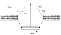
- the image sensor 432 may include an active area 432A configured to receive light and a peripheral area of the active area 432A.
- the active region 432A may have a substantially rectangular or square shape.
- the image sensor 432 and the spacer 440 may at least partially overlap.
- the active area 432A of the image sensor 432 may further extend outside the spacer 440
- the spacer 440 may further extend outside the active area 432A of the image sensor 432 . have.
- the active region 432A has a first edge P1 extending in a first length and a second edge P2 extending in a second length smaller than the first length and extending in a direction substantially perpendicular to the first edge P1.
- first edge P1 may extend in an x-axis direction (eg, a long side direction) and the second edge P2 may extend in a y-axis direction (eg, a short side direction).
- first edge P1 and the second edge P2 may be perpendicular to the direction of the optical axis OA.
- the center CA of the active area 432A may be defined as a center in each of a first edge direction (eg, a long side direction) and a second edge direction (eg, a short side direction).
- the image sensor 432 may be disposed such that the optical axis OA passes through the center CA of the active area 432A.
- the active region 432A may have a substantially rectangular shape having a first width W1 in the long side direction and a second width W2 smaller than the first width W1 in the short side direction.
- the center CS of the spacer 440 may be the center of a line connecting the center C1 of the first circular edge E1 and the center C2 of the second circular edge E2 illustrated in FIG. 7 .
- the spacer 440 may be disposed such that the optical axis OA passes through the center CS of the spacer 440 .
- the spacer 440 and the image sensor 432 may be disposed such that the center CS of the spacer 440 and the center CA of the active area 432A are positioned on the optical axis OA.
- the center CS of the spacer 440 and the center CA of the active region 432A may be aligned with the optical axis OA.
- the center CS of the spacer 440 is in a direction (eg, the first light of FIG. 5 ) toward the subject (eg, the subject 401 of FIG. 5 ) compared to the center CA of the active area 432A. It can be spaced apart in the axial direction (1)).
- the first reflected light 402 reflected from the first portion 440a of the spacer 440 is transmitted to another portion (eg, the second portion 440b of FIGS. 7 and 8A, 8B and 8C ). ), the possibility of being received in the active area 432A of the image sensor 432 may be higher than that of the second reflected light 403 reflected from the third portion 440c). For example, a portion of the first reflected light 402 may travel in a direction closer to the optical axis OA and the image sensor 432 .
- the image sensor 432 and the spacer 440 may be aligned in an additional method other than the center alignment CS, CA, and OA.
- the first portion 440a of the spacer 440 is positioned in the short-side direction (eg, the y-axis direction and the second width W2 direction) from the optical axis OA. can be arranged to do so.
- the first portion 440a of the spacer 440 may overlap an area adjacent to the first edge P1 (long side) of the active area 432A when viewed in the optical axis OA direction.
- the third portion 440c of the spacer 440 is positioned in the long side direction (eg, the x-axis direction and the first width W1 direction) from the optical axis OA. can be arranged to do so.
- the third portion 440b of the spacer 440 may overlap an area adjacent to the second edge P2 (short side) of the active area 432A when viewed in the optical axis OA direction.
- a first imaginary axis Y1 may be defined in the spacer 440 .
- the first virtual axis Y1 may be an axis that connects the first portion 440a of the spacer 440 and intersects the optical axis OA.
- the first imaginary axis Y1 may cross the opening area 448 and connect the first portion 440a of the spacer 440 .
- the spacer 440 and the image sensor 432 may be disposed such that the first virtual axis Y1 of the spacer 440 is parallel to the short side direction (eg, the y-axis direction) of the active region 432A.
- the spacer 440 may be disposed such that the first portion 440a faces in the short side direction (eg, the y-axis direction and the second width W2 direction).
- a second virtual axis X1 may be defined in the spacer 440 .
- the second virtual axis X1 may be an axis that connects the third portion 440c of the spacer 440 and intersects the optical axis OA.
- the spacer 440 and the image sensor 432 may be disposed such that the second virtual axis X1 of the spacer 440 is parallel to the long side direction (eg, the x-axis direction) of the active region 432A.
- the spacer 440 may be disposed such that the third portion 440c faces in the long side direction (eg, the x-axis direction and the first width W1 direction).
- a portion having a small width (eg, a second width W2 ) of the first portion 440a of the spacer 440 and the active area 432A overlaps each other.
- an indicator such as a notch (eg, a notch 449 in FIG. 6 ) may be formed in the spacer 440 .
- the notch 449 may be adjacent to the first portion 440a or spaced apart from the first portion 440a by a predetermined positional relationship (eg, circumferentially from the first portion 440a) by a predetermined angle. position) may be formed at a position having a predetermined positional relationship (eg, circumferentially from the first portion 440a) by a predetermined angle. position) may be formed at a position having a
- 11A is a diagram illustrating a part of a process of manufacturing a spacer of a camera module according to an exemplary embodiment.
- 11B is a diagram illustrating a part of a process of manufacturing a spacer of a camera module according to an exemplary embodiment.
- a method of manufacturing a spacer 440 may include preparing a plate 405 , and forming an opening region 448 in the plate 405 .
- Plate 405 may include a plurality of stacked layers.
- the stacked layer may include a base layer 471 and a coating layer 472 coated on at least one surface of the base layer 471 , as shown in FIGS. 8A , 8B and 8C .
- the base layer 471 may include a PET film or a PI film.
- the coating layer 472 may include a layer of black color.
- the coating layer 472 may include a carbon coating layer comprising carbon.
- the base layer 471 may include a metal layer including a metal material, and the coating layer 472 may be coated on at least one surface of the metal layer.
- the plate 405 may be formed of one metal layer.
- forming the opening region 448 in the plate 405 may include press working in which a partial region of the plate 405 is pressed using a mold 490 .
- the mold 490 may have a shape corresponding to the opening area 448 of the spacer 440 .
- the mold 490 may be configured to move in the press direction F.
- An opening region 448 of the spacer 440 may be formed by the mold 490 passing through the plate 405 in the press direction F.
- the plate 405 and the mold 490 may be disposed at a predetermined angle A.
- the plate 405 and the mold 490 may be arranged such that the normal vector n of the plate 405 and the press direction F of the mold 490 form a predetermined angle A. .
- the plate 405 is disposed on a horizontal jig facing the z-axis direction, and the mold 490 is moved in the press direction F having a predetermined angle A with respect to the z-axis.
- the plate 405 is disposed on a jig having a predetermined angle A with respect to the z-axis direction, and the mold 490 may move in a press direction F parallel to the z-axis.
- the predetermined angle A may be the same as the second inclination angle ⁇ 2 of the third portion 440c of the spacer 440 as shown in FIG. 8 .
- the mold 490 and the plate 405 are arranged to form a second inclination angle ⁇ 2 , and the mold 490 passes through the plate 405 , so that the second inclination angle with respect to the optical axis OA direction.
- An inner surface 453 of the third portion 440c having ( ⁇ 2) may be formed.
- the mold 490 may have a circular cross-section when viewed as a cross-section substantially perpendicular to the normal vector n of the plate 405 .
- the circular cross-section may have the same shape as the first circular edge E1 and the second circular edge E2 illustrated in FIG. 7 .
- the first diameter D1 of the circular cross section may be equal to twice the radius R of the first circular edge E1 and the second circular edge E2 .
- the mold 490 may have an elliptical cross-section when viewed in a cross-section perpendicular to the press direction F.
- a second diameter D2 and a third diameter D3 smaller than the second diameter D2 may be included.
- the second diameter D2 may be the same as the first diameter D1 of the circular cross-section.
- the second diameter D2 may be equal to twice the radius R of the first and second circular edges E1 and E2 illustrated in FIG. 7 .
- the third diameter D3 may be smaller than twice the radius R of the first and second circular edges E1 and E2 illustrated in FIG. 7 .
- a portion 491 connected by the second diameter D2 among the edges of the elliptical cross-section may form the first portion 440a of the spacer 440 illustrated in FIG. 7 .
- a portion 493 of the edge of the elliptical cross-section connected by the third diameter D3 may form the third portion 440c of the spacer 440 illustrated in FIG. 7 .
- the method of manufacturing the spacer 440 may further include an additional post-processing process performed to reduce reflectance after forming the opening region 448 in the plate 405 .
- An additional post-treatment process is a process (eg, anodizing) of forming a film on the metal region exposed to the inner surface 453 of the spacer 440 when the plate 405 includes a metal layer (eg, anodizing) or the inner surface of the spacer 440 . It may include a process of painting the metal area exposed to (453). For example, in the painting process, the light absorption may be improved and the reflectance may be reduced by painting with a black color.
- the additional post-treatment process may include a process of oxidizing a cross section of the PET film or the PI film exposed to the inner surface 453 of the spacer 440 .
- the spacer may be manufactured through a process of forming an opening region and a process of machining an inner surface of the opening region.
- the opening region 448 and the inner surface eg, FIG. 10A and The C-Cut of the first inner surface 453a and the second inner surface 453b of 10b may be simultaneously formed, thereby simplifying the manufacturing process of the spacer 440, thereby improving mass productivity and improving reliability. .
- FIG. 12 is a view illustrating a camera module and a spacer according to another embodiment.
- the camera module 500 includes a camera housing 510 , a reflective member 590 disposed inside the camera housing 510 , a lens assembly 530 , and an image sensor 532 .
- a light receiving area 512 into which light reflected or emitted from the subject 501 is incident may be formed on the first surface 511 of the camera housing 510 .
- the light receiving area 512 may be at least partially aligned with the reflective member 590 .
- the lens assembly 530 may include a plurality of lenses L1 , L2 , L3 , L4 , and L5 and a spacer 540 .
- the plurality of lenses L1, L2, L3, L4, and L5 may define an optical axis. At least a portion of the spacer 540 may be disposed between the lenses.
- the reflective member 590 may be disposed in the first optical axis direction (1) (eg, a direction close to the subject 501 ) with respect to the plurality of lenses L1 , L2 , L3 , L4 , and L5 .
- the reflective member 590 may be configured to reflect and/or refract light incident through the light receiving area 512 toward the lens assembly 530 .
- the reflective member 590 may include a first surface 591 aligned with the light receiving area 512 and a second surface 592 aligned with the optical axis OA.
- the second surface 592 may be located in the first optical axis direction (1) of the lens assembly 530 .
- the image sensor 532 may be disposed in the second optical axis direction (2) based on the plurality of lenses L1 , L2 , L3 , L4 , and L5 .
- the plurality of spacers 540 are disposed on the first surface 591 of the reflective member 590 and the first spacer 541 disposed adjacent to the light receiving area 512 and the second surface 592 of the reflective member 590 .
- a second spacer 542 disposed adjacently, a third spacer 543 disposed between the first lens L1 and the second lens L2, and between the third lens L3 and the fourth lens L4. It may include a fourth spacer 544 disposed on the .
- the first spacer 541 and the second spacer 542 may be positioned between the reflective member 590 and an internal structure (not shown) of the camera housing 510 to cushion the impact applied to the reflective member 590 .
- the first spacer 541 and/or the second spacer 542 may partially perform an diaphragm function.
- 13A is a view illustrating a spacer and an image sensor of a camera module according to another exemplary embodiment.
- 13B is a diagram illustrating a spacer and an image sensor of a camera module according to another exemplary embodiment.
- 14A is a view showing a cross-sectional view of a spacer and an image sensor of a camera module according to another embodiment.
- 14B is a cross-sectional view of a spacer and an image sensor of a camera module according to another embodiment.
- the image sensor 532 and/or the active region 532A of the image sensor 532 may be formed in a substantially rectangular shape.
- the image sensor 532 and/or the active area 532A of the image sensor 532 has a long side direction (eg, a horizontal direction with respect to the drawing) and a short side direction (eg, a vertical direction with respect to the drawing). can be defined.
- the active area 532A of the image sensor 532 may have a first width W1 in the long side direction and a second width W2 that is smaller than the first width W1 in the short side direction.
- the spacer 540 may be disposed to be at least partially aligned with the image sensor 532 .
- the spacer 540 and the image sensor 532 may be disposed such that the center CA of the active area 532A and the center CS of the spacer 540 coincide with the optical axis OA.
- the active area 532A of the image sensor 532 may further extend outside the spacer 540 , or the spacer 540 may further extend outside the active area 532A of the image sensor 532 . have.
- the opening region 548 of the spacer 540 When viewed in the optical axis OA direction, the opening region 548 of the spacer 540 has a pair of round first inner surfaces 551a and 551b facing each other, and a pair of first inner surfaces 551a and 551b. ) may be defined by a pair of second inner surfaces 552a and 552b connecting them.
- the second inner surfaces 552a and 552b may be formed in a straight line when viewed in the direction of the optical axis OA.
- a pattern 552p may be formed at least partially on the second inner surfaces 552a and 552b.
- the spacer 540 is disposed such that the pair of second inner surfaces 552a and 552b are substantially parallel to the long side direction of the image sensor 532 , and the pair of first inner surfaces 551a and 551b are connected to the image sensor 532 . may be disposed to face each other in the short side direction of the .
- the spacer 540 reduces light reflected from the inner surfaces 551a, 551b, 552a, and 552b of the spacer 540 and received into the active area 532A of the image sensor 532. It can be configured to Such reflected light (eg, the first reflected light 502 of FIGS. 14A and 14B ) is formed in a straight line (eg, FIG. 13B ) or a pattern 552p is formed (eg, FIG. 13A ) of a pair of second It may be more likely to be generated by the inner surfaces 552a and 552b.
- reflected light eg, the first reflected light 502 of FIGS. 14A and 14B
- a straight line eg, FIG. 13B
- a pattern 552p is formed (eg, FIG. 13A ) of a pair of second It may be more likely to be generated by the inner surfaces 552a and 552b.
- At least a portion of light passing through the opening 548 of the spacer 540 may be reflected by the pair of second inner surfaces 552a and 552b of the spacer 540 to be incident on the image sensor 532 .
- Such reflected light eg, the first reflected light 502 of FIGS. 14A and 14B
- Such reflected light may deteriorate image quality.
- the spacer 540 may be formed such that the pair of second inner surfaces 552a and 552b have a predetermined angle with respect to the optical axis OA in order to reduce the reflected light.
- the pair of second inner surfaces 552a and 552b may be formed to be parallel to each other and to have a designated angle other than 0 degrees with respect to the optical axis OA.
- the first reflected light 502 is reflected toward the outside of the edge of the active area 532A by the pair of inclined second inner surfaces 552a and 552b, or the active area 532A ) can be reflected away from
- the second reflected light 503 may be reflected toward the active region 532A, but a significant portion of the second reflected light 503 is an edge of the image sensor 532 in-active. It may be reflected toward a region (eg, a region excluding the active region 532A among the image sensors 532 of FIGS. 13A and 13B ) or may be reflected toward an edge of the active region 532A. Accordingly, the second reflected light 503 may have a relatively small effect on image quality.
- a pair of inclined second inner surfaces 552a and 552b of the spacer 540 may be disposed to face each other in a direction of a small width (eg, the second width W2 ) of the active region 532A. Accordingly, the camera module 500 can provide improved image quality by reducing the reflected light received by the image sensor 532 even when internal reflection occurs.
- An electronic device comprising: a camera module configured to receive external light through a portion of a surface of the electronic device, the camera module comprising: a camera housing, an image sensor disposed on a bottom surface of the camera housing; and a lens assembly, at least a portion of which is disposed inside the camera housing, the lens assembly including a first lens, a second lens, and a spacer disposed between the first lens and the second lens, wherein the spacer includes an optical axis
- An opening region through which the spacer passes may be formed, and the first inner surface and the second inner surface of the spacer may be formed in parallel when viewed from a cross-section including the optical axis.
- the spacer may include a first portion in which each of the first inner surface and the second inner surface is parallel to the optical axis.
- an inclination angle formed by the first inner surface and the second inner surface with the optical axis is defined, and the spacer is a circumference having the optical axis from the first portion as a center.
- the inclination angle may be formed to continuously increase or decrease as it goes along the direction.
- the spacer may include a second portion having the largest inclination angle, and the second portion may include a portion spaced apart from the first portion by substantially 90 degrees in the circumferential direction.
- the image sensor includes an active region in which the light passing through the first lens and the second lens is received, and the active region includes a first width measured in a first direction and a second width perpendicular to the first direction.
- a second width measured in a direction and smaller than the first width may be formed, and the image sensor may be disposed such that the optical axis passes through a center of the active region.
- the spacer may include a first portion in which each of the first inner surface and the second inner surface is parallel to the optical axis, and the first portion may be positioned in the second direction with respect to the optical axis.
- the spacer When the spacer is viewed as a cross-section including the optical axis, an inclination angle formed by the first inner surface and the second inner surface with the optical axis is defined, the spacer includes a second portion having the largest inclination angle, and The second portion may be positioned in the first direction with respect to the optical axis.
- the spacer includes a first surface at least partially in contact with the first lens and a second surface at least partially in contact with the second lens, wherein the first surface has a first circular rim defining the aperture area. is formed, and a second circular rim defining the opening region is formed on the second surface, and the spacer includes a line connecting the first center of the first circular rim and the second center of the second circular rim and the The optical axes may be arranged to cross each other.
- the spacer may include a notch formed adjacent to the first portion or spaced apart from the first portion at a predetermined angle.
- Each of the first lens and the second lens includes an optical portion configured to pass light reflected from a subject and a peripheral portion that is a peripheral portion of the optical portion, wherein the first surface is disposed on the peripheral portion of the first lens at least partially in contact, and the second surface may at least partially contact the peripheral portion of the second lens.
- the spacer may be arranged such that the aperture area is at least partially aligned with the optical portion of each of the first lens and the second lens in the optical axis direction.
- the spacer comprises a base layer and a coating layer disposed on at least one surface of the base layer, the base layer comprising a PET film and/or a PI film, the coating layer comprising the first lens or the second lens at least partially in contact with
- the coating layer may be black in color or may include carbon.
- the spacer may have a thickness of 0.01 mm or more and 0.2 mm or less, measured in the optical axis direction.
- the lens assembly may further include a lens barrel surrounding the first lens, the second lens, and the spacer, and a portion of the spacer may contact an inner surface of the lens barrel.
- a stepped structure may be formed on an inner surface of the lens barrel, and at least one of the spacer, the first lens, and the second lens may at least partially contact the stepped surface of the stepped structure.
- An air gap may be formed between the first lens and the second lens.
- the lens assembly may further include a plurality of spacers, and at least some of the plurality of spacers may function as an aperture of the camera module.
- the lens assembly may further include a plurality of lenses, and at least some of the plurality of spacers may extend between any one of the plurality of lenses and an inner surface of the lens barrel.
- the spacer is manufactured by penetrating the base layer using a press mold and the opening region is formed, and the base layer and the press mold are arranged so that the pressing direction of the press mold forms a predetermined angle with the base layer and the base layer may include at least one of PET, PI, and a metal.
- the opening region may be provided in a shape in which a length measured in a first direction is different from a length measured in a second direction perpendicular to the first direction when viewed in the optical axis direction.
- the spacer may include a curved section and a straight section when viewed in the optical axis direction.
- a pattern may be formed on at least one of the first inner surface and the second inner surface of the opening region.
- the camera module further includes a reflective member, at least a portion of which is disposed inside the camera housing, wherein the reflective member has a first surface facing the light-receiving area of the camera housing, and a second surface of the first lens and the reflective member It may be disposed to face the second lens.
- the camera module may further include a second spacer disposed adjacent to at least one of the first surface of the reflective member and the second surface of the reflective member.
- an (eg, first) component is referred to as being “connected (functionally or communicatively)” or “connected” to another (eg, second) component, that component is It may be directly connected to the component or may be connected through another component (eg, a third component).
- a device configured to may mean that the device is “capable of” with other devices or components.
- a processor configured (or configured to perform) A, B, and C refers to a processor dedicated to performing the operations (eg, an embedded processor), or stored in a memory device (eg, memory #30). By executing one or more programs, it may refer to a general-purpose processor (eg, CPU or AP) capable of performing corresponding operations.
- module includes a unit composed of hardware, software, or firmware, and may be used interchangeably with terms such as, for example, logic, logic block, component, or circuit.
- a “module” may be an integrally formed component or a minimum unit or a part of performing one or more functions.
- a “module” may be implemented mechanically or electronically, for example, known or to be developed, application-specific integrated circuit (ASIC) chips, field-programmable gate arrays (FPGAs), or It may include a programmable logic device.
- ASIC application-specific integrated circuit
- FPGAs field-programmable gate arrays
- an apparatus eg, modules or functions thereof
- method eg, operations
- a computer-readable storage medium eg, memory #30
- the instruction When the instruction is executed by a processor (eg, processor #20), the processor may perform a function corresponding to the instruction.
- Computer-readable recording media include hard disks, floppy disks, magnetic media (eg, magnetic tape), optical recording media (eg, CD-ROM, DVD, magneto-optical media (eg, floppy disks), built-in memory, etc.)
- An instruction may include code generated by a compiler or code that can be executed by an interpreter.
- Each component may be composed of a singular or a plurality of entities, and some sub-components among the aforementioned sub-components may be omitted or may further include other sub-components. .
- some components may be integrated into one entity to perform the same or similar functions performed by each corresponding component before being integrated. Operations performed by a module, program module, or other component may be executed sequentially, parallel, iteratively, or heuristically, or at least some operations may be executed in a different order, may be omitted, or other operations may be added. .
Landscapes
- Physics & Mathematics (AREA)
- Engineering & Computer Science (AREA)
- Multimedia (AREA)
- Signal Processing (AREA)
- General Physics & Mathematics (AREA)
- Optics & Photonics (AREA)
- Studio Devices (AREA)
- Credit Cards Or The Like (AREA)
Abstract
Description
Claims (15)
- 전자 장치에 있어서,상기 전자 장치는 상기 전자 장치의 표면의 일부를 통해 외부 광을 수신하도록 구성되는 카메라 모듈을 포함하고,상기 카메라 모듈은,카메라 하우징, 상기 카메라 하우징의 바닥면에는 이미지 센서가 배치됨; 및적어도 일부가 상기 카메라 하우징 내부에 배치되고, 제1 렌즈, 제2 렌즈, 및 상기 제1 렌즈와 상기 제2 렌즈 사이에 배치되는 스페이서를 포함하는 렌즈 어셈블리;를 포함하고,상기 스페이서에는 광 축이 통과하는 개구 영역이 형성되고,상기 스페이서는 상기 광 축을 포함하는 단면도에서, 상기 개구 영역의 제1 내면 및 제2 내면이 평행하게 형성되는 전자 장치.
- 청구항 1에 있어서,상기 제1 내면 및 상기 제2 내면 각각은 상기 광 축과 평행한 제1 부분을 포함하는 전자 장치.
- 청구항 2에 있어서,상기 광 축을 포함하는 단면도에서, 상기 제1 내면 및 상기 제2 내면이 상기 광 축과 형성하는 경사각이 규정되고,상기 스페이서는, 상기 제1 부분을 기준으로 상기 광 축을 중심으로 갖는 원의 원주 방향을 따라 갈수록 상기 경사각이 연속적으로 증가하거나 감소하도록 형성되는 전자 장치.
- 청구항 3에 있어서,상기 스페이서는 가장 큰 경사각을 가지는 제2 부분을 포함하고,상기 제2 부분은 상기 제1 부분으로부터 상기 원주 방향으로 실질적으로 90도만큼 이격된 부분을 포함하는 전자 장치.
- 청구항 1에 있어서,상기 이미지 센서는 상기 제1 렌즈 및 상기 제2 렌즈를 통과한 광이 수광되는 액티브 영역을 포함하고,상기 액티브 영역은 제1 방향으로 측정된 제1 폭, 및 상기 제1 방향에 수직한 제2 방향으로 측정되고 상기 제1 폭보다 작은 제2 폭을 가지도록 형성되고,상기 이미지 센서는 상기 광 축이 상기 액티브 영역의 중심을 통과하도록 배치되는 전자 장치.
- 청구항 5에 있어서,상기 스페이서는 상기 제1 내면 및 상기 제2 내면 각각이 상기 광 축과 평행한 제1 부분을 포함하고,상기 제1 부분은 상기 광 축을 기준으로 상기 제2 방향에 위치하는 전자 장치.
- 청구항 5에 있어서,상기 광 축을 포함하는 단면도에서, 상기 제1 내면 및 상기 제2 내면이 상기 광 축과 형성하는 경사각이 규정되고,상기 스페이서는 가장 큰 경사각을 가지는 제2 부분을 포함하고,상기 제2 부분은 상기 광 축을 기준으로 상기 제1 방향에 위치하는 전자 장치.
- 청구항 5에 있어서,상기 스페이서는 상기 제1 렌즈에 적어도 부분적으로 접촉하는 제1 면, 및 상기 제2 렌즈에 적어도 부분적으로 접촉하는 제2 면을 포함하고,상기 제1 면에는 상기 개구 영역을 규정하는 제1 원형 테두리가 형성되고,상기 제2 면에는 상기 개구 영역을 규정하는 제2 원형 테두리가 형성되고,상기 스페이서는 상기 제1 원형 테두리의 제1 중심 및 상기 제2 원형 테두리의 제2 중심을 연결하는 선과 상기 광 축이 교차하도록 배치되는 전자 장치.
- 청구항 6에 있어서,상기 스페이서는 상기 제1 부분에 인접하거나, 상기 제1 부분으로부터 사전에 결정된 각도로 이격된 위치에 형성되는 노치를 포함하는 전자 장치.
- 청구항 8에 있어서,상기 제1 렌즈 및 상기 제2 렌즈 각각은 피사체로부터 반사된 광이 통과하도록 구성되는 광학 부분 및 상기 광학 부분에 주변부인 주변 부분을 포함하고,상기 제1 면은 상기 제1 렌즈의 상기 주변 부분에 적어도 부분적으로 접촉하고,상기 제2 면은 상기 제2 렌즈의 상기 주변 부분에 적어도 부분적으로 접촉하는 전자 장치.
- 청구항 10에 있어서,상기 스페이서는 상기 개구 영역이 상기 제1 렌즈 및 상기 제2 렌즈 각각의 상기 광학 부분과 상기 광 축 방향으로 적어도 부분적으로 정렬되도록 배치되는 전자 장치.
- 청구항 1에 있어서,상기 스페이서는 베이스 레이어 및 상기 베이스 레이어의 적어도 일 표면에 배치되는 코팅 레이어를 포함하고,상기 베이스 레이어는 PET(polyethylene terephthalate) 필름 및 PI(polyimide) 필름 중 적어도 하나를 포함하고,상기 코팅 레이어는 상기 제1 렌즈 또는 상기 제2 렌즈와 적어도 부분적으로 접촉하는 전자 장치.
- 청구항 1에 있어서,상기 렌즈 어셈블리는 상기 제1 렌즈, 상기 제2 렌즈, 및 상기 스페이서를 둘러싸는 렌즈 배럴을 더 포함하고,상기 스페이서의 일부 영역은 상기 렌즈 배럴의 내면에 접촉하는 전자 장치.
- 청구항 13에 있어서,상기 렌즈 배럴의 내면에는 단차 구조가 형성되고,상기 스페이서, 상기 제1 렌즈, 또는 상기 제2 렌즈 중 적어도 하나는 상기 단차 구조의 단차면에 적어도 부분적으로 접촉하는 전자 장치.
- 청구항 1에 있어서,상기 제1 렌즈 및 상기 제2 렌즈 사이에는 에어갭이 형성되는 전자 장치.
Priority Applications (3)
| Application Number | Priority Date | Filing Date | Title |
|---|---|---|---|
| EP22759936.2A EP4258643A4 (en) | 2021-02-26 | 2022-02-09 | Camera module and electronic device comprising same |
| CN202280016902.7A CN116888971A (zh) | 2021-02-26 | 2022-02-09 | 相机模块和包括其的电子装置 |
| US17/681,042 US11994737B2 (en) | 2021-02-26 | 2022-02-25 | Camera module and electronic device including the same |
Applications Claiming Priority (2)
| Application Number | Priority Date | Filing Date | Title |
|---|---|---|---|
| KR10-2021-0026608 | 2021-02-26 | ||
| KR1020210026608A KR102887735B1 (ko) | 2021-02-26 | 2021-02-26 | 카메라 모듈 및 이를 포함하는 전자 장치 |
Related Child Applications (1)
| Application Number | Title | Priority Date | Filing Date |
|---|---|---|---|
| US17/681,042 Continuation US11994737B2 (en) | 2021-02-26 | 2022-02-25 | Camera module and electronic device including the same |
Publications (1)
| Publication Number | Publication Date |
|---|---|
| WO2022182018A1 true WO2022182018A1 (ko) | 2022-09-01 |
Family
ID=83048334
Family Applications (1)
| Application Number | Title | Priority Date | Filing Date |
|---|---|---|---|
| PCT/KR2022/001969 Ceased WO2022182018A1 (ko) | 2021-02-26 | 2022-02-09 | 카메라 모듈 및 이를 포함하는 전자 장치 |
Country Status (2)
| Country | Link |
|---|---|
| KR (1) | KR102887735B1 (ko) |
| WO (1) | WO2022182018A1 (ko) |
Families Citing this family (1)
| Publication number | Priority date | Publication date | Assignee | Title |
|---|---|---|---|---|
| KR20240037046A (ko) * | 2022-09-14 | 2024-03-21 | 엘지이노텍 주식회사 | 카메라 모듈 및 이를 구비한 차량 |
Citations (5)
| Publication number | Priority date | Publication date | Assignee | Title |
|---|---|---|---|---|
| KR101414826B1 (ko) * | 2014-03-28 | 2014-07-03 | (주)디지탈옵틱 | 렌즈 조립체 및 이를 구비하는 카메라 모듈 |
| KR20170000252A (ko) * | 2015-06-23 | 2017-01-02 | 삼성전기주식회사 | 렌즈 모듈 및 이를 포함하는 카메라 모듈 |
| KR20190070230A (ko) * | 2017-12-12 | 2019-06-20 | 삼성전기주식회사 | 렌즈 조립체 및 이를 포함하는 카메라 모듈 |
| KR20190111482A (ko) * | 2018-03-23 | 2019-10-02 | 엘지이노텍 주식회사 | 카메라 모듈 및 이를 포함하는 광학 기기 |
| KR20200076175A (ko) * | 2018-12-19 | 2020-06-29 | 주식회사 세코닉스 | 카메라 렌즈용 경통 조립체 |
Family Cites Families (4)
| Publication number | Priority date | Publication date | Assignee | Title |
|---|---|---|---|---|
| US9465187B2 (en) * | 2010-11-15 | 2016-10-11 | DigitalOptics Corporation MEMS | Thermal despace compensation systems and methods |
| KR101883033B1 (ko) * | 2015-05-27 | 2018-07-27 | 삼성전기주식회사 | 렌즈 모듈 |
| CN113341528B (zh) * | 2017-02-23 | 2023-01-31 | 核心光电有限公司 | 折叠式摄影机透镜设计 |
| KR101988602B1 (ko) * | 2017-09-14 | 2019-06-13 | 주식회사 나오텍 | Tof용 렌즈조립체 |
-
2021
- 2021-02-26 KR KR1020210026608A patent/KR102887735B1/ko active Active
-
2022
- 2022-02-09 WO PCT/KR2022/001969 patent/WO2022182018A1/ko not_active Ceased
Patent Citations (5)
| Publication number | Priority date | Publication date | Assignee | Title |
|---|---|---|---|---|
| KR101414826B1 (ko) * | 2014-03-28 | 2014-07-03 | (주)디지탈옵틱 | 렌즈 조립체 및 이를 구비하는 카메라 모듈 |
| KR20170000252A (ko) * | 2015-06-23 | 2017-01-02 | 삼성전기주식회사 | 렌즈 모듈 및 이를 포함하는 카메라 모듈 |
| KR20190070230A (ko) * | 2017-12-12 | 2019-06-20 | 삼성전기주식회사 | 렌즈 조립체 및 이를 포함하는 카메라 모듈 |
| KR20190111482A (ko) * | 2018-03-23 | 2019-10-02 | 엘지이노텍 주식회사 | 카메라 모듈 및 이를 포함하는 광학 기기 |
| KR20200076175A (ko) * | 2018-12-19 | 2020-06-29 | 주식회사 세코닉스 | 카메라 렌즈용 경통 조립체 |
Also Published As
| Publication number | Publication date |
|---|---|
| KR102887735B1 (ko) | 2025-11-19 |
| KR20220122237A (ko) | 2022-09-02 |
Similar Documents
| Publication | Publication Date | Title |
|---|---|---|
| WO2021141454A1 (en) | Camera module and electronic device including the same | |
| WO2023229150A1 (ko) | 렌즈 어셈블리 및 그를 포함하는 전자 장치 | |
| WO2022215943A1 (ko) | 카메라를 포함하는 전자 장치 및 그 전자 장치의 동작 방법 | |
| WO2022045702A1 (ko) | 이미지 안정화 어셈블리, 카메라 모듈 및 이를 포함하는 전자 장치 | |
| WO2023022438A1 (ko) | 폴디드 광학계를 포함하는 카메라 모듈 | |
| WO2022114789A1 (ko) | 광량을 획득하는 전자 장치 및 방법 | |
| WO2023018092A1 (ko) | 카메라 모듈을 포함하는 전자 장치 | |
| WO2023003322A1 (ko) | 카메라 모듈 및 이를 포함하는 전자 장치 | |
| WO2022182018A1 (ko) | 카메라 모듈 및 이를 포함하는 전자 장치 | |
| WO2022149714A1 (ko) | 전자 장치의 플래시 렌즈 | |
| WO2023158081A1 (ko) | 렌즈 어셈블리 및 그를 포함하는 전자 장치 | |
| WO2022255761A1 (ko) | 지문 센서를 포함하는 전자 장치 및 방법 | |
| WO2022220572A1 (ko) | 카메라 모듈 및 이를 포함하는 전자 장치 | |
| WO2022186511A1 (ko) | 후면 커버 및 카메라 모듈을 포함하는 전자 장치 | |
| WO2021210883A1 (ko) | 카메라 모듈 및 이를 포함하는 전자 장치 | |
| WO2023085650A1 (ko) | 카메라 모듈 및 이를 포함하는 전자 장치 | |
| WO2025033653A1 (ko) | 리플렉터, 리플렉터를 포함하는 카메라 모듈 및 카메라 모듈을 포함하는 전자 장치 | |
| WO2022225250A1 (ko) | 카메라 모듈 및 이를 포함하는 전자 장치 | |
| WO2025023453A1 (ko) | 카메라 모듈 및 이를 포함하는 전자 장치 | |
| WO2026043035A1 (ko) | 이미지 센서를 포함하는 전자 장치 | |
| WO2024225604A1 (ko) | 거리 측정 센서를 포함하는 전자 장치 | |
| WO2025053449A1 (ko) | 배플을 포함하는 카메라 모듈 및 이를 포함하는 전자 장치 | |
| WO2023096363A1 (ko) | 생체인증 장치를 포함하는 전자 장치 | |
| WO2024039016A1 (ko) | 렌즈들을 포함하는 카메라 및 이를 포함하는 전자 장치 | |
| WO2024071569A1 (ko) | 카메라 모듈을 지지하기 위한 구조를 포함하는 전자 장치 |
Legal Events
| Date | Code | Title | Description |
|---|---|---|---|
| 121 | Ep: the epo has been informed by wipo that ep was designated in this application |
Ref document number: 22759936 Country of ref document: EP Kind code of ref document: A1 |
|
| ENP | Entry into the national phase |
Ref document number: 2022759936 Country of ref document: EP Effective date: 20230704 |
|
| WWE | Wipo information: entry into national phase |
Ref document number: 202337053617 Country of ref document: IN |
|
| WWE | Wipo information: entry into national phase |
Ref document number: 202280016902.7 Country of ref document: CN |
|
| NENP | Non-entry into the national phase |
Ref country code: DE |