WO2022186385A1 - 周波数選択反射板および反射構造体 - Google Patents
周波数選択反射板および反射構造体 Download PDFInfo
- Publication number
- WO2022186385A1 WO2022186385A1 PCT/JP2022/009481 JP2022009481W WO2022186385A1 WO 2022186385 A1 WO2022186385 A1 WO 2022186385A1 JP 2022009481 W JP2022009481 W JP 2022009481W WO 2022186385 A1 WO2022186385 A1 WO 2022186385A1
- Authority
- WO
- WIPO (PCT)
- Prior art keywords
- thickness
- dielectric layer
- frequency selective
- selective reflector
- electromagnetic wave
- Prior art date
- Legal status (The legal status is an assumption and is not a legal conclusion. Google has not performed a legal analysis and makes no representation as to the accuracy of the status listed.)
- Ceased
Links
Images






Classifications
-
- H—ELECTRICITY
- H01—ELECTRIC ELEMENTS
- H01Q—ANTENNAS, i.e. RADIO AERIALS
- H01Q15/00—Devices for reflection, refraction, diffraction or polarisation of waves radiated from an antenna, e.g. quasi-optical devices
- H01Q15/0006—Devices acting selectively as reflecting surface, as diffracting or as refracting device, e.g. frequency filtering or angular spatial filtering devices
- H01Q15/0013—Devices acting selectively as reflecting surface, as diffracting or as refracting device, e.g. frequency filtering or angular spatial filtering devices said selective devices working as frequency-selective reflecting surfaces, e.g. FSS, dichroic plates, surfaces being partly transmissive and reflective
-
- H—ELECTRICITY
- H01—ELECTRIC ELEMENTS
- H01Q—ANTENNAS, i.e. RADIO AERIALS
- H01Q15/00—Devices for reflection, refraction, diffraction or polarisation of waves radiated from an antenna, e.g. quasi-optical devices
- H01Q15/0006—Devices acting selectively as reflecting surface, as diffracting or as refracting device, e.g. frequency filtering or angular spatial filtering devices
- H01Q15/0013—Devices acting selectively as reflecting surface, as diffracting or as refracting device, e.g. frequency filtering or angular spatial filtering devices said selective devices working as frequency-selective reflecting surfaces, e.g. FSS, dichroic plates, surfaces being partly transmissive and reflective
- H01Q15/0026—Devices acting selectively as reflecting surface, as diffracting or as refracting device, e.g. frequency filtering or angular spatial filtering devices said selective devices working as frequency-selective reflecting surfaces, e.g. FSS, dichroic plates, surfaces being partly transmissive and reflective said selective devices having a stacked geometry or having multiple layers
-
- H—ELECTRICITY
- H01—ELECTRIC ELEMENTS
- H01Q—ANTENNAS, i.e. RADIO AERIALS
- H01Q15/00—Devices for reflection, refraction, diffraction or polarisation of waves radiated from an antenna, e.g. quasi-optical devices
- H01Q15/14—Reflecting surfaces; Equivalent structures
-
- H—ELECTRICITY
- H01—ELECTRIC ELEMENTS
- H01Q—ANTENNAS, i.e. RADIO AERIALS
- H01Q3/00—Arrangements for changing or varying the orientation or the shape of the directional pattern of the waves radiated from an antenna or antenna system
- H01Q3/44—Arrangements for changing or varying the orientation or the shape of the directional pattern of the waves radiated from an antenna or antenna system varying the electric or magnetic characteristics of reflecting, refracting, or diffracting devices associated with the radiating element
- H01Q3/46—Active lenses or reflecting arrays
Definitions
- the present disclosure includes a frequency selective reflector that reflects electromagnetic waves in a specific frequency band in a direction different from the regular reflection direction, a frequency selective reflector, and a reflector having a protective member for protecting the frequency selective reflector.
- a frequency selective reflector that reflects electromagnetic waves in a specific frequency band in a direction different from the regular reflection direction
- a frequency selective reflector that reflects electromagnetic waves in a specific frequency band in a direction different from the regular reflection direction
- a frequency selective reflector and a reflector having a protective member for protecting the frequency selective reflector.
- Reflect array technology is being studied to improve the propagation environment and propagation area in mobile communication systems. Reflect array technology is described, for example, in Patent Literature 1 and Patent Literature 2, and Non-Patent Literature 1 and Non-Patent Literature 2.
- high-frequency radio waves such as those used in fifth-generation communication systems have a strong propagating property, so elimination of coverage holes is an important issue.
- a fifth generation communication system is also referred to as a 5G communication system.
- a coverage hole is an area where radio waves do not reach.
- the reflect array is desired to be able to reflect electromagnetic waves of a specific frequency incident from a base station in a predetermined direction in a desired direction.
- a reflect array for example, a plurality of reflective elements are arranged. By changing the size and shape of the reflective elements, the resonance frequency of each reflective element is changed to control the reflection phase of the electromagnetic wave.
- Techniques have been developed for controlling the incident and reflected directions of electromagnetic waves by controlling the reflection phase of the electromagnetic waves.
- the pattern of the reflective elements is formed by etching a metal layer using photolithography, for example.
- the reflection angle can be increased by, for example, narrowing the pitch of the reflecting elements.
- narrowing the pitch of the reflective elements in the planar arrangement of the reflective elements, it is difficult to increase the angle of reflection.
- there is a limit to the processing accuracy of photolithographic processing of metal layers it is difficult to finely control the reflection phase at high frequencies with short wavelengths that require processing accuracy.
- the present disclosure has been made in view of the above circumstances, and a primary object thereof is to provide a frequency selective reflector whose reflection characteristics can be easily customized.
- the reflect array needs to be protected from the external environment.
- the protective member is arranged in the reflect array, there is a problem that the electromagnetic wave is attenuated by the protective member.
- the thickness of the radome is 1/2 of the effective wavelength of electromagnetic waves or integral multiples thereof, or 1/4 of the effective wavelength of electromagnetic waves or integral multiples thereof.
- the distance between the antenna and the radome should be half the effective wavelength of the electromagnetic wave or an integer multiple thereof.
- the attenuation of electromagnetic waves by the protective member can be suppressed by setting the thickness of the protective member and the distance between the reflect array and the protective member to the specific values described above. It is possible. However, there are restrictions on the design of the reflect array and the protective member.
- the incident wave and the reflected wave have different path lengths between the incident side surface of the protective member and the reflect array surface. Therefore, when the protective member is arranged in the reflect array, even if the thickness of the protective member and the distance between the reflect array and the protective member are set to specific values as described above, the attenuation of electromagnetic waves by the protective member is sufficiently reduced. Uncontrollable.
- the present disclosure has been made in view of the above circumstances, and includes a frequency selective reflector that reflects electromagnetic waves in a specific frequency band in a direction different from the regular reflection direction, and a protective member for protecting the frequency selective reflector.
- a second object of the present invention is to provide a reflecting structure capable of suppressing attenuation of electromagnetic waves by a protective member without imposing restrictions on design.
- a primary object of the present disclosure is to provide a frequency selective reflector whose reflection characteristics can be easily customized.
- the first objective is achieved by the following embodiments of the present disclosure.
- One embodiment of the present disclosure is a frequency selective reflector that reflects electromagnetic waves in a specific frequency band of 24 GHz or higher in a direction different from the regular reflection direction, comprising: a reflecting member that reflects the electromagnetic waves; a dielectric layer that is arranged on the incident side of the electromagnetic wave, has an uneven structure in which a plurality of unit structures having a thickness distribution that increases in thickness in a predetermined direction is arranged, and transmits the electromagnetic wave.
- the unit structure of the dielectric layer has a plurality of cell regions with different thicknesses, and in each unit structure of the dielectric layer, the horizontal axis is the length of the unit structure in the predetermined direction, and the The vertical axis represents the relative reflection phase when the electromagnetic wave passes through the dielectric layer, is reflected by the reflecting member, passes through the dielectric layer again, and is emitted to the incident side of the electromagnetic wave, and the relative reflection phase of the electromagnetic wave.
- the points are on the same straight line, and the dielectric layer has, as the unit structure, three or more of the cell regions with different thicknesses.
- a frequency selective reflector which has at least a first unit structure and controls the reflection direction of the electromagnetic wave by controlling the relative reflection phase distribution of the electromagnetic wave by the thickness distribution of the dielectric layer.
- a frequency selective reflector that reflects electromagnetic waves in a specific frequency band of 24 GHz or higher in a direction different from the regular reflection direction, comprising: a reflecting member that reflects the electromagnetic waves; and a dielectric layer that is arranged on the incident side of the electromagnetic wave, has an uneven structure in which a plurality of unit structures having a thickness distribution that increases in thickness in a predetermined direction, and transmits the electromagnetic wave. and the unit structure of the dielectric layer has a plurality of cell regions with different thicknesses, and each unit structure of the dielectric layer has a minimum-thickness cell region with a minimum thickness in the predetermined direction.
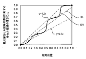
- the relative position is taken as the horizontal axis, and the thickness of the minimum thickness cell region is 0.
- the thickness of the maximum-thickness cell region is set to 1
- the ratio of the thickness of each cell region to the thickness of the maximum-thickness cell region is plotted on the vertical axis.
- a frequency selective reflector having at least a first unit structure having three or more cell regions with different thicknesses.
- a frequency selective reflector that reflects electromagnetic waves in a specific frequency band of 24 GHz or higher in a direction different from the regular reflection direction, comprising: a reflecting member that reflects the electromagnetic waves; and a dielectric layer that is arranged on the incident side of the electromagnetic wave, has an uneven structure in which a plurality of unit structures having a thickness distribution that increases in thickness in a predetermined direction, and transmits the electromagnetic wave. and the unit structure of the dielectric layer has a plurality of cell regions with different thicknesses, and in each unit structure of the dielectric layer, the difference between the minimum thickness and the maximum thickness is 0.2 mm or more and 15 mm or less. and wherein the dielectric layer has, as the unit structure, at least a first unit structure having three or more cell regions with different thicknesses.
- Another embodiment of the present disclosure provides a dielectric layer for use in the frequency selective reflector described above.
- the present disclosure provides a reflective structure having a frequency-selective reflector that reflects electromagnetic waves in a specific frequency band in a direction different from the regular reflection direction, and a protective member for protecting the frequency-selective reflector.
- a second object of the present invention is to provide a reflecting structure capable of suppressing the attenuation of electromagnetic waves by a protective member without giving any The second objective is achieved by the following embodiments of the present disclosure.
- Another embodiment of the present disclosure includes a frequency selective reflector that reflects electromagnetic waves in a specific frequency band in a direction different from the regular reflection direction, and a protective member disposed above the frequency selective reflector.
- a structure is provided, wherein the thickness of the protective member is less than 1/4 of the effective wavelength of the electromagnetic wave propagating in the protective member.
- the frequency selective reflector of the present disclosure has the effect of facilitating customization of reflection characteristics.
- the frequency selective reflector of the present disclosure has the effect of widening the margin of processing accuracy in controlling reflection characteristics.
- the reflecting structure of the present disclosure has the effect of being able to suppress the attenuation of electromagnetic waves by the protective member without imposing restrictions on the design.
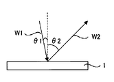
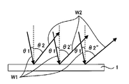
- FIG. 4 is a schematic diagram illustrating reflection characteristics of the frequency selective reflector of the present disclosure
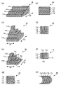
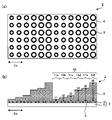
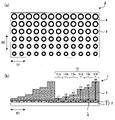
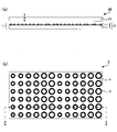
- 3A and 3B are a schematic perspective view and a plan view illustrating a unit structure of a dielectric layer in the frequency selective reflector of the present disclosure
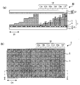
- FIG. 4 is a schematic plan view illustrating a unit structure of a dielectric layer in the frequency selective reflector of the present disclosure
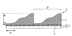
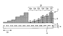
- 1 is a schematic cross-sectional view illustrating a frequency selective reflector of the present disclosure
- FIG. 1 is a schematic cross-sectional view illustrating a frequency selective reflector of the present disclosure, and a schematic diagram for explaining relative reflection phases of electromagnetic waves in each cell region of a unit structure of a dielectric layer in the frequency selective reflector of the present disclosure
- FIG. FIG. 4 is a schematic diagram illustrating reflection characteristics of the frequency selective reflector of the present disclosure
- FIG. 4 is a schematic plan view illustrating a unit structure of a dielectric layer in the frequency selective reflector of the present disclosure
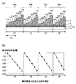
- 1 is a schematic cross-sectional view illustrating a frequency selective reflector of the present disclosure, and a schematic diagram for explaining relative reflection phases of electromagnetic waves in each cell region of a unit structure of a dielectric layer in the frequency selective reflector of the present disclosure
- FIG. 3 is a schematic diagram illustrating the configuration of a unit structure of a dielectric layer in the frequency selective reflector of the present disclosure
- 1 is a schematic cross-sectional view illustrating a frequency selective reflector of the present disclosure
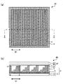
- FIG. 1A and 1B are a schematic plan view illustrating a reflecting member in a frequency selective reflector of the present disclosure and a schematic cross-sectional view illustrating the frequency selective reflector of the present disclosure
- FIG. 1A and 1B are a schematic plan view illustrating a reflecting member in a frequency selective reflector of the present disclosure and a schematic cross-sectional view illustrating the frequency selective reflector of the present disclosure
- FIG. 1 is a schematic cross-sectional view illustrating a frequency selective reflector of the present disclosure
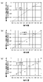
- FIG. 4 is a graph illustrating the relationship between the relative position and thickness ratio of each cell region of the unit structure of the dielectric layer in the frequency selective reflector of the present disclosure
- FIG. 2A is a schematic cross-sectional view illustrating a reflective structure of the present disclosure and a schematic plan view illustrating a frequency selective reflector in the reflective structure of the present disclosure
- FIG. 2A is a schematic cross-sectional view illustrating a reflective structure of the present disclosure and a schematic plan view illustrating a frequency selective reflector in the reflective structure of the present disclosure
- 1A and 1B are schematic plan and cross-sectional views illustrating reflective structures of the present disclosure
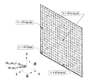
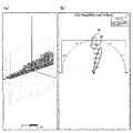
- 4 is a schematic perspective view showing a simulation model of Example 1 and a graph showing simulation results.
- FIG. 10 is a schematic perspective view showing a simulation model of Example 2 and a graph showing simulation results;
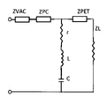
- FIG. It is a schematic diagram which illustrates a transmission-line equivalent circuit.
- FIG. 10 is a schematic perspective view showing a simulation model of Example 5 and a graph showing simulation results; 10 is a graph illustrating the relationship between the relative position and thickness ratio of each cell region of the unit structure of the dielectric layer in the frequency selective reflector of Example 6.
- FIG. 10 is a schematic perspective view showing a simulation model of Example 5 and a graph showing simulation results
- 10 is a graph illustrating the relationship between the relative position and thickness ratio of each cell
- the frequency selective reflector, the dielectric layer used therein, and the reflective structure in the present disclosure will be described in detail below.
- Frequency Selective Reflector The frequency selective reflector in this disclosure has three implementations. Hereinafter, each embodiment will be described separately.
- the frequency selective reflector of this embodiment is a frequency selective reflector that reflects electromagnetic waves in a specific frequency band of 24 GHz or higher in a direction different from the regular reflection direction, and the electromagnetic waves are a reflecting member for reflecting; and a dielectric layer that transmits the dielectric layer, wherein the unit structure of the dielectric layer has a plurality of cell regions with different thicknesses, and each unit structure of the dielectric layer includes the predetermined cell region of the unit structure.
- the horizontal axis represents the length in the direction of , and the relative reflection phase when the electromagnetic wave passes through the dielectric layer, is reflected by the reflecting member, passes through the dielectric layer again, and is emitted to the incident side of the electromagnetic wave.
- the vertical axis corresponds to the relative reflection phase of the electromagnetic wave at the center position of each cell region in the predetermined direction and the relative reflection phase of the electromagnetic wave at each cell region in a graph in which the value of the relative reflection phase of the electromagnetic wave is more than -360 degrees and 0 degrees or less. points are plotted and a straight line is drawn through the points corresponding to the minimum thickness cell regions having the minimum thickness. and controlling the reflection direction of the electromagnetic wave by controlling the relative reflection phase distribution of the electromagnetic wave according to the thickness distribution of the dielectric layer. It is something to do.
- the frequency selective reflector 1 includes a reflecting member 2 that reflects a specific electromagnetic wave, and a reflecting member 2 that is disposed on the side of the electromagnetic wave incident on the reflecting member 2, and extends in a predetermined direction D1.
- the frequency selective reflector 1 can also have an adhesive layer 6 between the reflector 2 and the dielectric layer 5 .
- the unit structure 10 of the dielectric layer 5 has a plurality of cell regions 11a-11f with different thicknesses t1-t6.
- the unit structure 10 of the dielectric layer 5 has a stepped shape in which the thicknesses t1 to t6 increase stepwise in a predetermined direction D1, and the number of steps of the stepped shape is six.
- the unit structure 10 of the dielectric layer 5 has six cell regions 11a to 11f. Since the cell regions 11a to 11f of the unit structure 10 of the dielectric layer 5 have different thicknesses t1 to t6, the electromagnetic waves pass through the dielectric layer 5, are reflected by the reflecting member 2, and pass through the dielectric layer 5 again.
- the reciprocating optical path lengths when emitted to the incident side of the electromagnetic wave are different, and the difference in the reciprocating optical path lengths in these dielectric layers, that is, the optical path difference, produces the difference in the relative reflection phase.
- optical path length is used because the wavelength of the frequency band targeted in the present disclosure is closer to light and has higher straightness compared to the conventional frequency band before LTE. Therefore, it is easier to explain behavior similar to that of light, and actually means the effective distance when an electromagnetic wave passes through the dielectric layer.
- the horizontal axis is the length L of the unit structure 10 in the predetermined direction D1.
- the vertical axis represents the relative reflection phase when the electromagnetic wave is transmitted and emitted to the incident side of the electromagnetic wave. Points corresponding to the relative reflection phase of the electromagnetic wave at the center position and each cell area are plotted, and when a straight line is drawn through the points corresponding to the minimum thickness cell area having the minimum thickness, each point is on the same straight line. be.
- the horizontal axis is the length L in the predetermined direction D1 of the unit structure 10 of the dielectric layer 5, and the electromagnetic wave passes through the dielectric layer 5, is reflected by the reflecting member 2, and passes through the dielectric layer 5 again.
- ) is an example of the relative reflection phase of electromagnetic waves in each cell region of the unit structure of the dielectric layer in the frequency selective reflector shown in FIG. As shown in FIG.
- the relative reflection phases of the electromagnetic waves in the respective cell regions 11a to 11f of the unit structure 10 of the dielectric layer 5 are 0 degrees, ⁇ 60 degrees, ⁇ 120 degrees, ⁇ 180 degrees, ⁇ 240 degrees and ⁇ 300 degrees, and the absolute value of the difference in the relative reflection phases of the electromagnetic waves in adjacent cell regions is 60 degrees.
- the thicknesses t1 to t6 of the six cell regions 11a to 11f of the unit structure 10 of the dielectric layer 5 are such that the absolute value of the difference between the relative reflection phases of the electromagnetic waves in adjacent cell regions is 360 degrees. It is designed to be a value divided by 60 degrees.
- the relative reflection phase of the electromagnetic wave at the center position in the predetermined direction D1 of each of the cell regions 11a to 11f of the unit structure 10 of the dielectric layer 5 and each of the cell regions 11a to 11f is
- the points are on the same straight line. That is, each point is on the solid line in the graph shown in FIG. 1(c).
- reflection phase refers to the amount of change in the phase of a reflected wave with respect to the phase of an incident wave incident on a certain surface.
- the phase of the incident wave when the incident wave is transmitted through the dielectric layer, reflected by the reflecting member, transmitted again through the dielectric layer and emitted is the amount of change in the phase of the reflected wave.
- the term "relative reflection phase” refers to a reflection phase in a cell region having the smallest reflection phase delay in one unit structure of a dielectric layer, and a certain The negative sign indicates the delay of the reflection phase in the cell area. For example, in one unit structure of the dielectric layer, if the reflection phase in the cell region with the smallest reflection phase delay is -10 degrees, the relative reflection phase in the cell region with the reflection phase of -40 degrees is - 30 degrees.
- the relative reflection phase of electromagnetic waves in the cell area is a value obtained by combining the reflection phases of the reflecting members.
- cell region refers to a region in which the relative reflection phases of electromagnetic waves are the same in the unit structure of the dielectric layer.
- the reflection phase is within the range of more than -360 degrees and less than +360 degrees, and -360 degrees and +360 degrees return to 0 degrees unless otherwise specified.
- the relative reflection phase is within the range of more than -360 degrees and less than or equal to 0 degrees, and -360 degrees returns to 0 degrees.
- the reflection phase can be delayed or advanced by adjusting the size and shape of the reflective elements.
- the reflection phase is basically delayed by adjusting the thickness of each cell region of the unit structure of the dielectric layer. Therefore, the relative reflection phase is based on the reflection phase in the cell region with the smallest delay in the reflection phase.
- the cell region with the smallest reflection phase delay is usually the minimum thickness cell region having the minimum thickness in a predetermined direction of increasing thickness. Therefore, in the above graph, a straight line is drawn through the points corresponding to the minimum thickness cell regions having the minimum thickness.
- the thicknesses t1 to t6 change, so that the round-trip optical path length in the dielectric layer 5 changes, and the relative reflection of electromagnetic waves Phase changes. Therefore, as illustrated in FIG. 2, the incident wave W1 of the electromagnetic wave can be reflected in a specular reflection direction, ie, a direction different from the specular reflection direction. In this case, the incident angle ⁇ 1 of the incident wave W1 of the electromagnetic wave and the reflection angle ⁇ 2 of the reflected wave W2 of the electromagnetic wave are different.
- the frequency selective reflector of this embodiment by changing the thickness of each cell region of the unit structure of the dielectric layer, the round-trip optical path length in the dielectric layer is changed for each cell region, and the electromagnetic wave is reflected. Phase can be controlled. Thereby, the reflection direction with respect to the predetermined incident direction of the electromagnetic wave can be controlled in any direction.
- the uneven structure of the dielectric layer in this embodiment can be formed by various methods such as cutting, laser processing, molding using a mold, 3D printer, joining of small parts, and the like. Therefore, the photomask required for photolithographic processing of the metal layer in the conventional reflect array is not required. Therefore, when forming the dielectric layer by designing the thickness of each cell region of the unit structure of the dielectric layer so as to achieve the reflection characteristics with the desired incident angle and reflection angle according to the situation, A desired dielectric layer can be formed at low cost and in a short period of time, and it is possible to easily meet the needs of small-lot production of a wide variety of products.
- the thickness of the dielectric layer and the size of the unit structure of the dielectric layer which affect the control of the reflection characteristics, can be processed in a relatively wide range. Therefore, for example, the incident angle and the reflection angle of the electromagnetic wave can be increased, and the control range of the reflection characteristics can be widened. Furthermore, regarding the thickness of the dielectric layer and the pitch of the cell regions of the unit structure of the dielectric layer, the margin of dimensional processing accuracy for realizing the desired reflection phase is relatively wide. Therefore, desired reflection characteristics can be easily obtained, and the influence of dimensional variations can be reduced. Therefore, it is easy to customize the reflective properties of the frequency selective reflector.
- the reflective member can be a frequency selective plate that reflects only specific electromagnetic waves.
- the reflecting member 2 is formed by arranging a plurality of ring-shaped reflecting elements 3, a dielectric substrate 4, and a dielectric layer of the dielectric substrate 4. It has a plurality of reflective elements 3 arranged on the surface on the 5 side.
- the reflective member is a frequency selective plate that reflects only a specific electromagnetic wave, and can be a member that has a reflection phase control function of controlling the reflection phase of the electromagnetic wave.
- a reflecting member can change the resonance frequency of each reflecting element by changing the size and shape of the reflecting element, and can control the reflection phase of the target electromagnetic wave.
- the reflection phase of the electromagnetic wave can be controlled not only by the thickness of the dielectric layer but also by the size and shape of the reflecting element, and the degree of freedom in designing the control of the reflection characteristics can be improved.
- the frequency selective reflector of the present embodiment when using the reflecting member as described above, it is possible to expand the degree of freedom in controlling the reflection characteristics by combining it with the dielectric layer. Therefore, it is possible to more easily customize the reflection characteristics of the frequency selective reflector. For example, there is an operation in which a plurality of types of reflecting members are prepared for reflection characteristics in the vertical direction and combined with a dielectric layer that adjusts the reflection characteristics in the horizontal direction.
- the inventors of the present disclosure have found that, in the frequency selective reflector having a reflecting member and a dielectric layer of the present disclosure, when the reflecting member is a frequency selective plate having a reflecting element that reflects only a specific electromagnetic wave, We simulated the reflection characteristics of electromagnetic waves in specific frequency bands. By this simulation, the thickness of the cell region of the unit structure of the dielectric layer is changed rather than the reflection phase shift in the reflecting element due to the proximity of the dielectric layer to the reflective member, that is, the frequency selection plate. First, it was found that the reflection phase shift is larger when the round-trip optical path length in the dielectric layer is changed. In other words, the inventors have found that the design of substantial reflection characteristics can be almost determined by the design of the uneven structure of the dielectric layer.
- the resonance frequency of the reflective element fluctuates depending on the presence or absence of the adjacent dielectric layer. Furthermore, the in-plane arrangement of the concave-convex structure of the dielectric layer that realizes the in-plane distribution design of the reflection phase in the frequency selective reflector does not need to have a fixed positional relationship with the in-plane arrangement of the reflecting elements of the reflecting member. , it was found that even if the concave-convex structure of the dielectric layer is displaced with respect to the in-plane arrangement of the reflective element, the reflection characteristics are not significantly affected.
- the dielectric layer and the reflecting member when the dielectric layer and the reflecting member are combined, the dielectric layer and the reflecting member can be designed independently and combined. be.
- a dielectric layer that achieves reflection characteristics according to the use environment may be produced each time, or a plurality of specifications may be prepared in advance. Therefore, the design of the reflection direction of the frequency selective reflector, which changes according to the environment of use, can be customized more easily, facilitating application to various situations.
- the arrangement of the reflective member and the dielectric layer can be made according to the required specifications. Accuracy of displacement is required.
- the reflection characteristics of the frequency selective reflector are adjusted only by the reflection phase distribution of the dielectric layer, the accuracy of misalignment between the reflecting member and the dielectric layer is not so required.
- the dielectric layer in this embodiment is arranged on the electromagnetic wave incident side with respect to the reflecting member, and has an uneven structure in which a plurality of unit structures having a thickness distribution in which the thickness increases in a predetermined direction are arranged. It is a member that transmits electromagnetic waves in a specific frequency band.
- the unit structure of the dielectric layer has a plurality of cell regions with different thicknesses.
- the horizontal axis is the length of the unit structure in a predetermined direction
- the electromagnetic wave is a dielectric.
- the vertical axis represents the relative reflection phase when it is transmitted through the body layer, reflected by the reflecting member, transmitted through the dielectric layer again, and emitted to the incident side of the electromagnetic wave.
- the dielectric layer has at least a first unit structure having three or more cell regions with different thicknesses as a unit structure.
- the dielectric layer has an uneven structure in which a plurality of unit structures having a thickness distribution in which the thickness increases in a predetermined direction are arranged.
- the unit structure of the dielectric layer has a plurality of cell regions with different thicknesses.
- the horizontal axis is the length of the unit structure in the predetermined direction, and the electromagnetic waves are generated in the dielectric.
- the vertical axis represents the relative reflection phase when it is transmitted through the layer, reflected by the reflective member, transmitted through the dielectric layer again, and emitted to the incident side of the electromagnetic wave, and the value of the relative reflection phase of the electromagnetic wave is more than -360 degrees and 0 degrees or less.
- each point being on the same straight line means that the difference in the vertical axis direction of each point with respect to the straight line is within ⁇ 72 degrees.
- the difference in the vertical axis direction of each point with respect to the straight line is preferably within ⁇ 54 degrees, more preferably within ⁇ 36 degrees, and even more preferably within ⁇ 18 degrees.
- each point includes a deviation in the vertical axis direction from the above straight line and it is difficult to draw a straight line passing through each point, "the point corresponding to the minimum thickness cell region having the minimum thickness and a point corresponding to the minimum thickness cell region having the minimum thickness in the adjacent unit features.
- a point corresponding to a minimum thickness cell region having a minimum thickness is a point with a relative reflection phase of 0 degrees.
- the point corresponding to the minimum thickness cell region having the minimum thickness in the unit features adjacent to that unit feature is the point that can be regarded as the relative reflection phase of -360 degrees.
- the unit structure of the dielectric layer has a thickness distribution in which the thickness increases in a predetermined direction.
- a unit structure of the dielectric layer may have, for example, a thickness distribution in which the thickness increases only in one direction.
- the unit structure of the dielectric layer may have a thickness distribution in which the thickness increases in two directions: a first direction and a second direction perpendicular to the first direction.
- FIG. 3A shows an example in which the unit structure 10 of the dielectric layer has a thickness distribution in which the thickness increases only in the first direction D1
- FIGS. a) is an example in which the unit structure 10 of the dielectric layer has a thickness distribution in which the thickness increases in the first direction D1 and the second direction D2.
- the points are plotted on the above graph with the horizontal axis representing the length of the unit structure in that one direction, the points are on the same straight line.
- the unit structure of the dielectric layer has a thickness distribution in which the thickness increases in two directions perpendicular to each other, the above points are plotted on the above graph in which the horizontal axes are the lengths of the unit structures in the two directions. When plotted, each point will be on the same straight line in each graph.
- the absolute value of the difference in the relative reflection phases of electromagnetic waves between adjacent cell regions is less than 180 degrees, preferably 120 degrees or less, and preferably 60 degrees or less. more preferred.
- the absolute value of the difference in the relative reflection phases of the electromagnetic waves in adjacent cell regions is greater than 0 degree.
- the relative reflection phase of the electromagnetic wave in the minimum thickness cell region having the minimum thickness in the other unit structure is calculated for one period based on the reflection phase in the cell region with the smallest reflection phase delay in one unit structure.
- the relative reflection phase of an electromagnetic wave in the maximum thickness cell region having the maximum thickness in one unit structure and the minimum thickness in the other unit structure when shown at more than -720 degrees and less than or equal to -360 degrees shifted by
- the absolute value of the difference from the relative reflection phase of the electromagnetic wave in the minimum thickness cell region is less than 180 degrees, preferably 120 degrees or less, more preferably 60 degrees or less.
- the absolute value of the difference in the relative reflection phases of the electromagnetic waves in these adjacent cell regions is greater than 0 degrees.
- the relative reflection phase of the electromagnetic wave in the maximum thickness cell region 11f having the maximum thickness t6 of one unit structure 10a is ⁇ 300 degrees.
- the relative reflection phase of the electromagnetic wave in the minimum thickness cell region 11a having the minimum thickness t1 of the other unit structure 10b is -360 degrees. Therefore, the relative reflection phase of the electromagnetic wave in the maximum thickness cell region 11f having the maximum thickness t6 of one unit structure 10a and the electromagnetic wave in the minimum thickness cell region 11a having the minimum thickness t1 of the other unit structure 10b is 60 degrees.
- the difference in the relative reflection phases of electromagnetic waves in adjacent cell regions be equal.
- the unit structure 10 of the dielectric layer 5 has six cell regions as shown in FIG.
- a difference in relative phase reflection of electromagnetic waves in the cell regions 11b and 11c, a difference in relative phase reflection of electromagnetic waves in the adjacent cell regions 11c and 11d, and a difference in relative phase reflection of electromagnetic waves in the adjacent cell regions 11d and 11e. and the difference in the relative reflection phases of the electromagnetic waves in the adjacent cell regions 11e and 11f are preferably equal to each other.
- the absolute values of the differences in the relative reflection phases of the electromagnetic waves in the adjacent cell regions are all 60 degrees and are equal.
- the relative reflection phase of the electromagnetic wave in the minimum thickness cell region having the minimum thickness in the other unit structure is calculated for one period based on the reflection phase in the cell region with the smallest reflection phase delay in one unit structure.
- the minimum thickness cell areas with the minimum thickness in the other unit feature when shown at more than -720 degrees and less than or equal to -360 degrees offset, adjacent It is preferable that the difference in the relative reflection phases of the electromagnetic waves in the cell regions that are the same. For example, in FIG.
- the relative reflection phases of electromagnetic waves in the respective cell regions 11a to 11f of one unit structure 10a are 0 degree, -60 degrees, and -120 degrees. -180 degrees, -240 degrees, and -300 degrees, and the relative reflection phase of the electromagnetic wave in the minimum thickness cell region 11a having the minimum thickness t1 of the other unit structure 10b is -360 degrees. Therefore, all the cell regions 11a to 11f in one unit structure 10a and the minimum thickness cell region 11a having the minimum thickness t1 in the other unit structure 10b are included in the adjacent cell regions.
- the absolute values of the relative reflection phase differences are all 60 degrees and are equal.
- the relative reflection phase of the electromagnetic wave in the minimum thickness cell region having the minimum thickness and the relative reflection phase of the electromagnetic wave in the maximum thickness cell region having the maximum thickness The absolute value of the difference is less than 360 degrees. In one unit structure of the dielectric layer, the relative reflection phase of the electromagnetic wave in the minimum thickness cell region having the minimum thickness and the relative reflection phase of the electromagnetic wave in the maximum thickness cell region having the maximum thickness
- the absolute value of the difference must be greater than 180 degrees, and more preferably 300 degrees or more and less than 360 degrees. For example, when the unit structure 10 of the dielectric layer 5 has six cell regions, as shown in FIG. is preferably less than 360 degrees. For example, in FIG.
- the relative reflection phase of the electromagnetic wave in the minimum thickness cell region 11a having the minimum thickness t1 is 0 degrees
- the relative reflection phase of the electromagnetic wave at the maximum thickness cell region 11f having t6 is -300 degrees
- the absolute value of the difference from the relative reflection phase of the electromagnetic wave in the maximum thickness cell region 11f is 300 degrees.
- the size of the unit structure of the dielectric layer is appropriately set according to the desired reflection characteristics.
- the length of the unit structure in a given direction of increasing thickness will shift the phase by one wavelength, or 360 degrees, and thus the angle of reflection can be adjusted.
- the difference between the angle of reflection relative to the angle of specular reflection can be increased.
- the difference between the angle of reflection and the angle of regular reflection can be reduced.
- the cross-sectional shape of the unit structure of the dielectric layer may be, for example, a stepped shape in which the thickness increases stepwise in a predetermined direction, or a step shape in which the thickness gradually increases in a predetermined direction. It may be tapered.
- FIG. 1B shows an example in which the unit structure 10 of the dielectric layer 5 has a stepped shape
- FIG. 5 shows an example in which the unit structure 10 of the dielectric layer 5 has a tapered shape.
- the unit structure of the dielectric layer has a plurality of cell regions with different thicknesses.
- the cross-sectional shape of the unit structure of the dielectric layer has a tapered shape, the number of cell regions in the unit structure is infinitely increased. can be regarded as Even in this case, the thickness distribution of the unit structure is designed so that the relative reflection phase of electromagnetic waves in each cell region is set as described above.
- the pattern shape of the unit structures in a plan view may be any shape as long as it can be arranged without gaps. Examples include a rectangular shape, a regular hexagonal shape, and the like.
- FIGS. 3A to 3F and FIG. 4A are examples in which the pattern shape of the unit structure 10 of the dielectric layer is rectangular in plan view.
- the difference in round-trip optical path length between adjacent cell regions is designed so that the relative reflection phases of electromagnetic waves in each cell region are set as described above.
- the thickness of each cell region is set so that the difference in thickness between adjacent cell regions equals the difference in round-trip optical path length between the adjacent cell regions.
- the thickness of each cell region is appropriately set according to the wavelength of the electromagnetic wave, the dielectric constant of the material of the dielectric layer, and the desired reflection characteristics. For example, when the effective wavelength of an electromagnetic wave passing through the dielectric is ⁇ g and the thickness of the base is ⁇ , the thickness of each cell region is preferably about ⁇ + 0 ⁇ g or more and ⁇ + 2 ⁇ g or less.
- the thickness ⁇ of the base can be the same as the minimum thickness of the minimum thickness cell region having the minimum thickness in one unit structure of the dielectric layer.
- the thickness ⁇ of the base is appropriately set in consideration of the overall strength, easiness of formation, etc. However, in consideration of the influence on electromagnetic waves, it is usually preferably about 0.1 ⁇ g or less. Specifically, when the wavelength ⁇ 0 of the electromagnetic wave in the air is 10 mm and the dielectric constant of the dielectric layer is 2.57, the thickness of each cell region should be 0 mm or more and 8.6 mm or less. is preferred. In addition, the case where the thickness of the cell region is 0 mm means that the dielectric layer is not formed in the cell region located on the reflective member.
- the difference between the minimum thickness and the maximum thickness is, for example, preferably 0.2 mm or more and 15 mm or less, and more preferably 2.1 mm or more and 10.4 mm or less.
- the difference between the minimum thickness and the maximum thickness is too large, the thickness of the entire frequency-selective reflector will increase, which may restrict installation and may make handling difficult. Moreover, there is a possibility that the manufacturing cost increases.
- the higher the dielectric constant of the dielectric layer the greater the dielectric loss, and the greater the reflection at the dielectric interface. As a result, reflections in the design direction are reduced. Therefore, if the difference between the minimum thickness and the maximum thickness is too small, losses including dielectric loss and interfacial reflection may increase.
- the minimum thickness and maximum thickness of the unit structure of the dielectric layer refer to the minimum thickness and maximum thickness of one unit structure of the dielectric layer as a whole. For example, as shown in FIG. 1(b), when the unit structure 10 of the dielectric layer 5 has six cell regions 11a-11f, the minimum thickness is t1 and the maximum thickness is t6. For example, as shown in FIG. 5, when the unit structure 10 of the dielectric layer 5 has a tapered shape, the minimum thickness is ta and the maximum thickness is tb.
- the difference between the minimum thickness and the maximum thickness in the unit structure of the dielectric layer is, for example, a value measured using a thickness measurement method with a thickness resolution of about 1 ⁇ m. Further, for example, the difference between the minimum thickness and the maximum thickness may be a value obtained by observing a cross section in the thickness direction of the unit structure of the dielectric layer and measuring it with an optical microscope.
- the pitch and width of the cell regions are appropriately set.
- the pitch of the cell regions of the unit structure of the dielectric layer may be the same as or different from the pitch of the reflecting elements of the reflecting member. good.
- the pitch of the cell regions of the unit structure of the dielectric layer is the same as the pitch of the reflective elements of the reflective member, the design is facilitated. Further, for example, by narrowing the pitch of the cell regions of the unit structure of the dielectric layer while maintaining the difference in the relative reflection phase of the electromagnetic waves in the adjacent cell regions, , the control range of the reflection characteristics can be widened.
- the pitches of the cell regions are preferably equal.
- the pitch of the cell area means the distance from the center of one cell area to the center of the adjacent cell area.
- the width of the cell region in a predetermined direction in which the thickness increases is equal.
- the pattern shape of the cell region in plan view includes, for example, a stripe shape, a shape obtained by dividing a concentric square into four equal parts by straight lines parallel to the sides and perpendicular to each other, a microarray shape, and a concentric circle.
- a stripe shape a shape obtained by dividing a concentric square into four equal parts by straight lines parallel to the sides and perpendicular to each other
- a microarray shape and a concentric circle.
- FIG. 3B shows an example of stripes.
- FIG. 3(d) is an example of one shape when a concentric square is divided into four equal parts by straight lines parallel to the sides and perpendicular to each other.
- FIGS. 3(f) and 4(a) are examples of microarrays.
- FIG. 4B is an example of concentric quadrants.
- FIG. 4(c) is an example of curved steps.
- FIG. 3(b) is a top view of FIG. 3(a).
- FIG. 3(d) is a top view of FIG. 3(c).
- FIG. 3(f) is a top view of FIG. 3(e).
- the direction of arrangement For example, rectangular unit structures may be arranged on the entire surface while being rotated 30 degrees clockwise in plan view. It is also possible to arrange the unit structures by selecting an appropriate angle and an appropriate arrangement direction according to the required reflection characteristic design.
- a unit structure of a dielectric layer has a plurality of cell regions.
- the number of cell regions is, for example, 3 or more, and may be 6 or more.
- the greater the number of cell regions in one unit structure of the dielectric layer the smaller the difference in the relative reflection phase of the electromagnetic wave between adjacent cell regions, and the smoother the wavefront of the reflected wave.
- the cross-sectional shape of the unit structure is a stepped shape
- the number of cell regions corresponds to the number of steps of the stepped shape.
- the cross-sectional shape of the unit structure is tapered, as described above, the tapered shape can be regarded as infinitely increasing the number of cell regions.
- the dielectric layer has, as a unit structure, at least a first unit structure having three or more cell regions with different thicknesses.
- the dielectric layer may have only the first unit structure as a unit structure, or may further have a second unit structure different from the first unit structure. That is, the dielectric layers may have only the same unit structure as the unit structure, or may have different unit structures. If the dielectric layer is formed by arranging a plurality of different unit structures, it can affect the overall reflection characteristics of the frequency selective reflector. Specifically, adjustment of polarization characteristics, influence on beam profile, and the like are exemplified. The influence on the beam profile means, for example, making a highly directional beam, making a diffuse beam, making a multi-beam, or the like.
- the first unit structure and the second unit structure can have different reflection characteristics. For example, at least one of the length of the unit structure in the direction of increasing thickness, the thickness distribution, the number, width, and pitch of the cell regions, the pattern shape of the unit structure when viewed in plan, and the pattern shape of the cell region when viewed in plan. can be different.
- the number of types of unit structures is not particularly limited.
- the thickness distribution of the dielectric layer is appropriately selected so that the normal vector of the same phase plane of the reflected wave with respect to the incident wave at a predetermined incident angle is in a desired reflection direction.
- the unit structure For example, when an incident wave is reflected in a single direction, that is, as a so-called plane wave, the dielectric layer is preferably composed of a plurality of identical unit structures, and the unit structure in the direction in which the thickness increases. More preferably, the lengths of the structures are the same, and the pattern shape of the cell region in plan view is striped. For example, in FIGS.
- the dielectric layer 5 has only a plurality of identical unit structures, the lengths L of the unit structures 10a and 10b in the predetermined direction D1 are the same, and the cell
- the pattern shape of the regions 11a to 11f in plan view is a stripe shape.
- an incident wave W1 incident at a predetermined incident angle ⁇ 1 can be reflected at a single reflection angle ⁇ 2, and the reflected wave W2 can be a plane wave without spreading.
- FIG. 1(a) shows an arrangement in which the longitudinal direction of the stripes in the cell region is parallel to the short direction of the wavelength selective reflector. In the reflector, the longitudinal direction and lateral direction of the stripes in the cell region can be arbitrarily set according to the design of the reflection characteristics.
- the dielectric layer preferably has a plurality of unit structures that are different from each other.
- the lengths are different
- the pattern shape of the cell region in a plan view is a stripe shape.
- the dielectric layer 5 has three different types of unit structures 10a and 10b, 10c and 10d.
- the lengths L1, L2 and L3 of the unit structures in the predetermined direction D1 are different from each other, and the numbers of the cell regions 11a to 11g, 12a to 12f and 13a to 13e are different from each other.
- the relative reflection phases of electromagnetic waves in the respective cell regions 11a to 11g of the unit structure 10a are 0 degree, -51.4 degrees, -103 degrees, -154 degrees, -206 degrees, -257 degrees, and -309 degrees
- the relative reflection phases of electromagnetic waves in the cell regions 12a to 12f of the unit structures 10b and 10c are 0 degrees, -60 degrees, -120 degrees, and -180 degrees, respectively.
- the relative reflection phases of the electromagnetic waves in the respective cell regions 13a to 13e of the unit structure 10d are 0 degrees, -72 degrees, -144 degrees, -216 degrees, and -288 degrees, respectively.
- the unit structures 10a and 10b, and 10c and 10d have different reflection characteristics.
- the pattern shape of the cell regions 11a to 11g, 12a to 12f, and 13a to 13e in plan view is a stripe shape.
- an incident wave W1 incident at a predetermined incident angle ⁇ 1 can be reflected at reflection angles ⁇ 2, ⁇ 2′, and ⁇ 2′′ depending on the unit structure, and can be reflected with a spread. It is possible to widen the wavefront of the reflected wave W2.
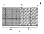
- the dielectric layer has unit structures different from each other as unit structures, a plurality of types of unit structures having different reflection characteristics are used, a plurality of unit structures are arranged for each type, and a plurality of unit structures of the same type are arranged. You may planarly arrange the area
- the dielectric layer 5 is formed by planarly arranging the arranged second regions 5b. In such an aspect, it is possible to deal with a plurality of coverage holes.
- the reflecting member described later is a frequency selective plate and has a plurality of types of frequency selective surfaces that selectively reflect electromagnetic waves in different frequency bands, depending on the frequency selectivity of those frequency selective surfaces.
- the reflection characteristics of the unit structures may be designed, and the dielectric layer may be used as the unit structure to have unit structures having different reflection characteristics.
- an arrangement as shown in FIG. 8 can be adopted. In such an embodiment, dual bands or more bands can be supported.
- the dielectric layer has unit structures different from each other as unit structures, for example, the relative reflection phase of the electromagnetic wave in each cell region of the n unit structures is shifted by n wavelengths due to the n unit structures. may be set.
- the phase difference is n ⁇ 360 degrees.
- n is an integer of 2 or more.
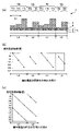
- the dielectric layer 5 has two different types of unit structures 10a and 10b. This is an example in which relative reflection phases of electromagnetic waves are set in respective cell regions 11a to 11c and 12a to 12b of two unit structures 10a and 10b. In this case, the phase difference is 720 degrees. Note that FIG.
- FIG. 9B is a graph showing the range of the relative reflection phase of the electromagnetic wave as more than -360 degrees and 0 degrees or less, and FIG. It is 0 degree or less, and is a graph obtained by interpolating points of substantially the same phase where the relative reflection phase is shifted by 360 degrees.
- These unit structures 10a and 10b have different lengths L1 and L2 in the predetermined direction D1, and different numbers of cell regions 11a to 11c and 12a to 12b.
- one unit structure 10a has three cell regions 11a to 11c, while the other unit structure 10b has two cell regions 12a and 12b.
- at least one type of unit structure may have three or more cell regions with different thicknesses.
- the number of cell regions in the unit structure is not limited to three or more, and may be two.
- the dielectric layer has a periodic structure in which unit structures are repeatedly arranged.
- the term “periodic structure” refers to a structure in which unit structures are periodically and repeatedly arranged.
- the length of the unit structure in the direction of increasing thickness, thickness distribution, number of cell regions, width, pitch, and planar view pattern of the unit structure The shape, the pattern shape in plan view of the cell area, and the like can be made the same.
- unit structures having different reflection characteristics can be combined as described above. In that case, the reflection characteristics of the unit structure to be combined are appropriately designed according to the target reflection characteristics.
- the number, width, and pitch of the regions, the pattern shape of the unit structure in plan view, the pattern shape of the cell region in plan view, and the like are appropriately set according to the desired reflection characteristics.
- the reflection characteristic design for reflecting a plane wave as a plane wave in a direction different from the specular reflection direction for example, after decomposing the incident/reflection characteristics in the in-plane x-direction and in-plane y-direction of the reflector plate, the x-direction.
- Designing is possible by converting it into a reflection phase distribution in the y direction and incorporating it as the thickness distribution of the unit structure.
- the 10 ⁇ 10 size of the cell area is not necessarily the size of the unit structure.
- Reflection phase ⁇ required for the cell region at position (i, j) when a plane wave incident from the direction of the incident angle ( ⁇ in , ⁇ in ) is reflected as a plane wave in the direction of the reflection angle ( ⁇ out , ⁇ out ) i and j are given by the following equations.
- ⁇ i,j 2 ⁇ p ⁇ i ⁇ (sin ⁇ out ⁇ cos ⁇ out ⁇ sin ⁇ in ⁇ cos ⁇ in )+ p ⁇ j ⁇ (sin ⁇ out ⁇ sin ⁇ out ⁇ sin ⁇ in ⁇ sin ⁇ in ) ⁇ / ⁇
- ⁇ i,j reflection phase of the cell area at position (i, j) with respect to phase center (0, 0)
- ⁇ wavelength of reflected wave [m]
- p size of cell area [m] ⁇ in : ⁇ tilt of incident wave ⁇ in : ⁇ tilt of incident wave ⁇ out : ⁇ tilt of reflected wave ⁇ out : ⁇ tilt of reflected wave.
- the dielectric layer may be, for example, a single layer or multiple layers. Further, the dielectric layer may have a substrate portion serving as a base and uneven portions arranged on the substrate portion. Further, the dielectric layer may be, for example, a single member in which all the cell regions are formed integrally, or each cell region is separately formed and block-shaped cell regions are arranged. can be anything.
- the dielectric layer may transmit electromagnetic waves in a specific frequency band, and may or may not transmit electromagnetic waves in other frequency bands.
- the dielectric loss tangent of the dielectric layer is preferably relatively small. Since the dielectric loss tangent of the dielectric layer is small, the dielectric loss can be reduced, and the high frequency loss can be reduced. Specifically, the dielectric loss tangent of the dielectric layer to electromagnetic waves of the target frequency is preferably 0.01 or less. Moreover, the dielectric loss tangent of the dielectric layer is preferably as small as possible, and the lower limit is not particularly limited.
- the dielectric layer has a relatively high dielectric constant. Since the dielectric layer has a high dielectric constant, an effect of reducing the thickness of the dielectric layer can be expected.
- the dielectric constant of the dielectric layer for electromagnetic waves of the target frequency is preferably 2 or more, more preferably 2.5 or more. It is more preferably 3 or more.
- the dielectric loss tangent and dielectric constant of the dielectric layer can be measured by the resonator method.
- the material of the dielectric layer is not particularly limited as long as it is a dielectric that can transmit predetermined electromagnetic waves.
- resin, glass, quartz, ceramics, etc. can be used. can be done. Among them, resin is preferable in consideration of the ease of forming the concave-convex structure.
- the resin is not particularly limited as long as it can transmit a predetermined electromagnetic wave, but it is preferable that the resin absorb relatively little electromagnetic wave and have relatively high transmittance of the electromagnetic wave. Moreover, the resin preferably satisfies the above dielectric loss tangent, and more preferably satisfies the above dielectric constant. Examples of such resins include polycarbonates, acrylic resins, ABS resins, PLA resins, olefinic resins, and copolymers thereof. Among them, polycarbonate is preferable because of its excellent dimensional stability and low high-frequency loss.
- the dielectric layer can further contain a filler.
- filler By including filler in the dielectric layer, the dielectric constant and mechanical strength of the dielectric layer can be adjusted.
- the dielectric constant of the filler is preferably higher than that of the resin. Thereby, the dielectric constant of the dielectric layer can be increased, and the required thickness of the dielectric layer can be reduced.
- the high dielectric constant filler is not particularly limited, and examples thereof include glass, silica, inorganic particles such as barium titanate, and fine fibers.
- the material, shape, size, and content of the filler can be appropriately selected according to the desired dielectric constant, mechanical strength, difficulty of dispersibility, and the like.
- the size of the filler must be sufficiently smaller than the wavelength of the target electromagnetic wave, and when the effective wavelength of the electromagnetic wave is ⁇ g , the diameter of the filler equivalent to a sphere is preferably 0.01 ⁇ g or less, for example.
- the size of the filler approaches the order of nanometers, it tends to become difficult to uniformly disperse the filler, which may increase the processing load.
- the content of the filler in the dielectric layer varies depending on the combination of materials of the dielectric and the filler, the shape of the filler, the size of the filler, and the like, and is appropriately adjusted.
- the concave-convex structure of the dielectric layer is formed by molding using a mold, for example, a release agent, an antistatic agent, or the like may be added to the dielectric layer. These can be used by appropriately selecting general ones. Moreover, it is preferable that the dielectric layer does not contain additives or fillers that impart electrical conductivity, such as carbon black or metal particles.
- the method for forming the dielectric layer is not particularly limited as long as it is a method capable of forming a predetermined concave-convex structure. , molding using a mold, vacuum casting, modeling using a 3D printer, bonding of small parts, and the like.
- molding methods that do not use molds, such as cutting, laser processing, and 3D printers, it is easy to customize according to the desired angle of reflection, so special installation situations and large-scale projects that are difficult to simulate are possible. It can also be suitably used for design tuning when designing and developing a wavelength-selective reflector.
- the molding may be performed on a substrate made of a dielectric material. material may be used.
- a plurality of types of dielectric layers having reflection characteristics that provide predetermined angles of incidence and reflection are prepared in advance, and the dielectric layers are prepared according to the situation. and rotate the dielectric layer in the plane with the normal direction as the axis for fine adjustment of the reflection direction of the electromagnetic waves. It may be advantageous in terms of cost to manufacture them all at once, and in that case, a molding technique using a mold is suitable.
- the reflective member in this embodiment is a member that reflects electromagnetic waves in a specific frequency band.
- the reflecting member is not particularly limited as long as it reflects electromagnetic waves in a specific frequency band.
- it may reflect only electromagnetic waves in a specific frequency band, or It may be one that reflects not only electromagnetic waves in one frequency band but also electromagnetic waves in other frequency bands.
- the reflecting member preferably has a wavelength selection function of reflecting only electromagnetic waves in a specific frequency band.
- FIG. 11 shows an example in which the reflective member 2 is the reflective layer 7 .
- the reflective layer 7 is arranged over the entire surface of the frequency selective reflector 1 .
- the material of the reflective layer is not particularly limited as long as it can reflect electromagnetic waves in a specific frequency band, and examples thereof include conductive materials such as metal materials, carbon, and ITO.
- the thickness of the reflective layer is not particularly limited as long as it can reflect electromagnetic waves in a specific frequency band, and is set as appropriate.
- the reflective member may be a frequency selective plate.
- a frequency selective plate has a frequency selective surface that controls the reflection and transmission of electromagnetic waves in a specific frequency band.
- a frequency selective surface is also called FSS or Frequency Selective Surface.
- the frequency selection plate may have a plurality of reflective elements or scattering elements arranged in its plane.
- the frequency selection plate may have, for example, a dielectric substrate and a plurality of reflective elements arranged on the surface of the dielectric substrate on the dielectric layer side.
- FIG. 1B shows an example in which the reflecting member 2 is a frequency selection plate.
- the reflecting member 2 includes a dielectric substrate 4 and a plurality of reflectors arranged on the surface of the dielectric substrate 4 on the dielectric layer 5 side. element 3.
- the frequency selection plate may be appropriately selected from known frequency selection plates and used.
- the shape of the reflective element that forms the frequency selective surface may be a planar pattern shape.
- the planar pattern shape may be, for example, a ring shape, a cross shape, a square shape, a rectangular shape, a circular shape, an elliptical shape, a rod shape, a pattern shape divided into a plurality of adjacent regions, or the like.
- the shape of the reflective element forming the frequency selective surface may be a three-dimensional shape.
- the three-dimensional shape may be a through-hole via, or the like.
- the reflective element may be, for example, a single layer or a multilayer.
- the frequency selection plate may be, for example, a dielectric substrate with a plurality of reflective elements arranged on one side thereof.
- the frequency selection plate is, for example, a plate in which a plurality of reflective elements are arranged on both sides of a dielectric substrate, or a structure in which a dielectric substrate, a plurality of reflective elements, a dielectric substrate, and a plurality of reflective elements are arranged. It may be one arranged in order, or one in which a conductor is arranged on one surface farthest from the surface on the side of incidence of electromagnetic waves.
- the frequency selection plate that is, the reflecting member preferably has a reflection phase control function of controlling the reflection phase of electromagnetic waves.
- the reflective member may have reflective elements that vary in size and/or shape. The change in dimensions of the reflective elements may be gradual contraction or expansion. By changing the size and shape of the reflecting elements, the resonance frequency can be changed for each reflecting element, and the reflection phase of the electromagnetic wave can be controlled. Therefore, when the frequency selection plate has a reflection phase control function, the reflection characteristics of the electromagnetic wave can be controlled by controlling the reflection phase distribution of the electromagnetic wave according to the thickness of the dielectric layer and the dimensions and shape of the reflective element.
- the reflection characteristics in two orthogonal directions in the plane of the frequency selective reflector can be individually designed for the frequency selection plate and the dielectric layer, and the desired electromagnetic wave reflection characteristics can be achieved while suppressing the thickness of the dielectric layer.
- the two orthogonal directions may be, for example, the x-axis direction and the y-axis direction.
- a general frequency selective surface can be applied as a frequency selective plate having a reflection phase control function. These have advantages and disadvantages in design, but all of them are capable of changing the reflection phase of electromagnetic waves by changing the dimensions and shape of the reflecting element.
- Different dimensions of the reflective element are appropriately selected according to the shape of the reflective element.
- the thickness of each cell region of the unit structure of the dielectric layer is changed to change the round-trip optical path length in the dielectric layer for each cell region.
- the relative reflected phase of the electromagnetic wave can be controlled.
- the direction of reflection of electromagnetic waves incident from a predetermined direction can be controlled. can do.
- the reflecting member is a frequency selection plate and a member having a reflective phase control function
- the thickness of each cell region of the unit structure of the dielectric layer is changed so that the dielectric layer is formed in each cell region.
- the resonance frequency of each reflecting element can be changed, and the reflection phase of the electromagnetic wave can be controlled. Therefore, it is possible to expand the degree of freedom in designing the reflection characteristic control.
- the reflection control direction in the reflecting member and the reflection control direction in the dielectric layer it is also possible to separate the reflection control direction in the reflecting member and the reflection control direction in the dielectric layer, and perform two-dimensional reflection direction control in the entire frequency selective reflector. Further, when the reflection control directions of the reflecting member and the dielectric layer overlap, for example, a reflection phase distribution that reflects light in a direction determined to some extent can be realized by the reflecting member, and fine adjustment can be made by the dielectric layer. . In this case, there is an advantage that the thickness of the dielectric layer can be reduced.
- Dielectric layer 5 and reflective member 2 may be arranged such that cell regions 11a-11f of structure 10 have a greater thickness.
- the thickness of the dielectric layer can be suppressed.
- the dielectric layer becomes thinner, so that the weight and cost of the frequency selective reflector can be reduced, and even when the angle of reflection is large, the reflected wave is less likely to strike the dielectric layer.
- the dielectric layer 5 and the reflecting member 2 may be arranged so that the thickness of the cell regions 11a to 11f of the unit structure 10 of the dielectric layer 5 increases along the direction D1 perpendicular to the direction D2.
- the dielectric layer is rotated in-plane with respect to the reflective member about the normal direction, so that the dielectric layer is rotated with respect to the reflective member.
- the reflection characteristics can be controlled by adjusting the length of the unit structure in a predetermined direction in which the thickness increases. For example, by shortening the length of the unit structure in the predetermined direction of increasing thickness, the angle of reflection of the electromagnetic wave can be increased, while the length of the unit structure in the predetermined direction of increasing thickness can be increased. By increasing the length, the angle of reflection of electromagnetic waves can be reduced.
- the length of the unit structure in a predetermined direction in which the thickness increases means that the unit structure of the dielectric layer has a thickness distribution in which the thickness increases in a predetermined direction. , refers to the length of the unit structure in that given direction.
- the thickness of the unit structure 10 of the dielectric layer 5 increases in the predetermined direction D1
- the length of the unit structure 10 in the predetermined direction D1 is L.
- the in-plane arrangement of the uneven structure of the dielectric layer that realizes the in-plane distribution design of the reflection phase in the frequency selective reflector has a certain positional relationship with the in-plane arrangement of the reflecting elements of the reflecting member. is not necessary, and even if the concave-convex structure of the dielectric layer is displaced from the in-plane arrangement of the reflective element, the reflection characteristics are not significantly affected. Therefore, when the reflective member is a frequency selection plate and a member having a reflective phase control function, it is possible to design the dielectric layer and the reflective member independently.
- the frequency-selective reflector of this embodiment may have other configurations in addition to the reflecting member and dielectric layer described above, if necessary.
- the frequency selective reflector of the present disclosure may have an adhesive layer between the reflecting member and the dielectric layer.
- An adhesive layer may adhere the reflective member and the dielectric layer.
- the adhesive layer can flatten the unevenness caused by the reflecting elements, and the reflecting elements when laminating the dielectric layer on the reflecting member. It is possible to suppress the influence of unevenness due to For example, in FIG. 1B, an adhesive layer 6 is arranged between the reflecting member 2 and the dielectric layer 5 .
- an adhesive or a pressure-sensitive adhesive can be used for the adhesive layer, and can be appropriately selected from known adhesives and pressure-sensitive adhesives.
- the adhesive or pressure-sensitive adhesive must be a non-conductor.
- the adhesive or pressure-sensitive adhesive is liquid, it is preferable that it has fluidity to the extent that it can be spread evenly and air bubbles can be removed.
- the adhesive or pressure-sensitive adhesive is in the form of a sheet, it is preferable that the thickness is uniform, and the flexibility is such that it can follow the unevenness of the lamination interface and suppress the entrapment of air bubbles. It is preferable to have
- the thickness of the adhesive layer is such that a desired adhesive force can be obtained, and is preferably uniform.
- the thickness of the adhesive layer is preferably equal to or greater than the thickness of the reflecting elements from the viewpoint of planarization. At this time, if the adhesive layer is thicker than the reflective element, the reflective element is embedded in the adhesive layer.
- the thickness of the adhesive layer is preferably sufficiently smaller than the effective wavelength of the target electromagnetic wave. .
- the frequency selective reflector of the present disclosure may have a space between the reflecting member and the dielectric layer.
- a space 8 is arranged between the reflective member 2 and the dielectric layer 5 .
- the distance between the reflective member and the dielectric layer is preferably constant. Thereby, the optical path lengths in the space can be made uniform.
- the frequency selective reflector of the present disclosure may have a cover member on the surface of the dielectric layer opposite to the reflecting member.
- the dielectric layer can be protected by the cover member.
- designability can be imparted by the cover member.
- the frequency selective reflector of the present disclosure may have a ground layer on the surface of the reflecting member opposite to the dielectric layer.
- the ground layer blocks interference with objects on the back side of the frequency-selective reflector and suppresses the generation of noise.
- the ground layer can also be part of a reflective member that has no wavelength selectivity. As the ground layer, it is sufficient if it has conductivity, and for example, a general conductive layer such as a metal plate, metal layer, metal mesh, carbon, or ITO film can be used.
- the frequency selective reflector of the present disclosure may have a flattening layer between the reflecting member and the dielectric layer.
- the flattening layer can flatten the unevenness caused by the reflective elements, and the reflective elements when laminating the dielectric layer on the reflective member The influence of unevenness can be suppressed.
- the flattening layer here refers to a layer that is arranged separately from the adhesive layer, and can be exemplified by an ionizing radiation curable resin layer that is arranged so as to embed the reflecting element. Further, in the case of a form in which a space is provided between the reflective member and the dielectric layer, the flattening layer may have the function of protecting the reflective element.
- a fixing layer for attaching the frequency selective reflector is provided on the surface of the reflection member opposite to the dielectric layer.
- An anchoring layer with features may be arranged.
- a metal layer may be arranged between the fixed layer and the reflecting member, or the fixed layer may also serve as the metal layer.
- the fixed layer has a frequency It may have a mechanism for varying the angle of the normal direction of the selective reflector.
- Antireflection layer In the case of high frequencies, the influence of reflection at the dielectric layer interface can be considered, so in the frequency selective reflector of the present disclosure, if necessary, the A barrier layer may be arranged.
- the antireflection layer may have, for example, a multilayer structure with different dielectric constants, or may have an uneven structure smaller than the wavelength of the electromagnetic wave.
- the frequency selective reflector of the present disclosure reflects electromagnetic waves in a specific frequency band of 24 GHz or higher in a direction different from the regular reflection direction.
- the frequency band of the electromagnetic wave is not particularly limited as long as it is 24 GHz or higher, but it is preferably in the range of 24 GHz or higher and 300 GHz or lower. If the frequency band of the electromagnetic wave is within the above range, the frequency selective reflector of the present disclosure can be used for the fifth generation mobile communication system, so-called 5G.
- the frequency selective reflector of the present disclosure can be used, for example, as a frequency selective reflector for communication, and is particularly suitable as a frequency selective reflector for mobile communication.
- the frequency selective reflector of this embodiment is a frequency selective reflector that reflects electromagnetic waves in a specific frequency band of 24 GHz or higher in a direction different from the regular reflection direction, and the electromagnetic waves are a reflecting member for reflecting; and a dielectric layer that transmits the dielectric layer, wherein the unit structure of the dielectric layer has a plurality of cell regions with different thicknesses, and each unit structure of the dielectric layer has a minimum thickness of When the center position of the thickness cell region in the predetermined direction is 0, and the center position of the maximum thickness cell region having the maximum thickness in the predetermined direction is 1, the relative position is taken as the horizontal axis, and the minimum When the thickness of the thickness cell region is 0 and the thickness of the maximum thickness cell region is 1, the ratio of the thickness of each cell region to the thickness of the maximum thickness cell region is plotted on the vertical axis.
- the frequency selective reflector of this embodiment controls the relative reflection phase distribution of the electromagnetic wave by the thickness distribution of the dielectric layer, thereby reflecting the electromagnetic wave. Control direction.
- FIGS. 15(a) and (b) are a schematic plan view and a cross-sectional view showing an example of the frequency selective reflector of this embodiment
- FIG. 15(b) is a cross-sectional view taken along the line AA of FIG. 15(a). is.
- the frequency selective reflector 1 is arranged with a reflecting member 2 that reflects a specific electromagnetic wave, and is arranged on the side of the reflecting member 2 on which the electromagnetic waves are incident, and is arranged in a predetermined direction D1.
- the frequency selective reflector 1 can also have an adhesive layer 6 between the reflector 2 and the dielectric layer 5 .
- the unit structure 10 of the dielectric layer 5 has a plurality of cell regions 11a-11d with different thicknesses t1-t4.
- the unit structure 10 of the dielectric layer 5 has a stepped shape in which the thicknesses t1 to t4 increase stepwise in a predetermined direction D1, and the number of steps in the stepped shape is four.
- the unit structure 10 of the dielectric layer 5 has four cell regions 11a to 11d. Since the cell regions 11a to 11d of the unit structure 10 of the dielectric layer 5 have different thicknesses t1 to t4, the electromagnetic waves pass through the dielectric layer 5, are reflected by the reflecting member 2, and pass through the dielectric layer 5 again.
- the reciprocating optical path lengths when emitted to the incident side of the electromagnetic wave are different, and the difference in the reciprocating optical path lengths in these dielectric layers, that is, the optical path difference, produces the difference in the relative reflection phase.
- the thicknesses t1 to t4 change, so that the round-trip optical path length in the dielectric layer 5 changes, and the relative reflection phase of the electromagnetic wave changes, as illustrated in FIG. 2, the incident wave W1 of the electromagnetic wave can be reflected in a direction different from the regular reflection (specular reflection) direction.
- the incident angle ⁇ 1 of the incident wave W1 of the electromagnetic wave and the reflection angle ⁇ 2 of the reflected wave W2 of the electromagnetic wave are different.
- the center position P0 in the predetermined direction D1 of the minimum thickness cell region 11a having the minimum thickness t1 is 0
- the maximum thickness cell region 11d having the maximum thickness t4 is 0
- the horizontal axis represents the relative position in the predetermined direction D1 when the central position P1 in the predetermined direction D1 is 1
- the thickness t1 of the minimum thickness cell region 11a is 0,
- the maximum thickness cell region 11d is When the thickness t4 is set to 1, the ratio of the thicknesses t1 to t4 of the cell regions 11a to 11d to the thickness t4 of the maximum thickness cell region 11d is plotted on the vertical axis.
- FIG. 15(c) shows, when the center position P0 of the minimum thickness cell region 11a in the predetermined direction D1 is 0 and the center position P1 of the maximum thickness cell region 11d in the predetermined direction D1 is 1 ,
- the thickness t1 of the minimum thickness cell region 11a is 0, and the thickness t4 of the maximum thickness cell region 11d is 1, the thickness t4 of the maximum thickness cell region 11d is plotted.
- 15(a) and 15(b) is a graph showing the ratio of the thicknesses t1 to t4 of the cell regions 11a to 11d on the vertical axis, showing the relationship between the cell regions of the unit structure of the dielectric layer in the frequency selective reflector shown in FIGS. 15(a) and (b). Examples of position and thickness ratios.
- the center position Px is obtained by the following formula (2).
- P x (distance between P x and P 0 in a given direction)/(distance between P 1 and P 0 in a given direction) (2)
- the relative positions of the center positions of the cell regions 11a to 11d in the unit structure 10 of the dielectric layer 5 in the predetermined direction D1 are 0, 0.33, 0.67 and 1, respectively.
- the thickness ratio (T 2 ⁇ T 1 )/(T 4 ⁇ T 1 ).
- the thickness ratio (T 3 -T 1 )/(T 4 -T 1 ).
- the vertical axis and horizontal axis are the same as those in FIG. , are examples of design values DV.
- the design value DV is usually indicated by a curved line.
- the measured value is in good agreement with the design value DV. Therefore, it is conceivable to derive a regression curve from the measured values.
- the curve of the design value DV is appropriately set according to the wavelength of the electromagnetic wave, the dielectric constant of the dielectric layer, the desired reflection characteristics, and the like. Therefore, it is difficult to derive the regression curve from the measured values, and it is also difficult to derive the regression curve from the measured values and evaluate the difference from the design values. Therefore, in this embodiment, the regression line is obtained from the measured values.
- the coefficient of determination R2 of the regression line is set to 0.9 or more, and the slope a of the regression line is set to 0.7 or more and 1.2 or less. If the coefficient of determination R2 of the regression line is a predetermined value or more and the slope a of the regression line is within a predetermined range, the difference between the actual measurement value and the design value should be within a predetermined range. can be done.
- the frequency selective reflector of this embodiment by changing the thickness of each cell region of the unit structure of the dielectric layer, the round-trip optical path length in the dielectric layer is changed for each cell region, and the electromagnetic waves are emitted. Reflection phase can be controlled. Further, by setting the slope of the regression line and the coefficient of determination obtained as described above within a predetermined range, a desired reflection phase can be obtained. Thereby, the reflection direction with respect to the predetermined incident direction of the electromagnetic wave can be controlled in any direction.
- the frequency selective reflector of this embodiment can achieve the same effect as the frequency selective reflector of the first embodiment.
- the dielectric layer in this embodiment is arranged on the electromagnetic wave incident side with respect to the reflecting member, and has an uneven structure in which a plurality of unit structures having a thickness distribution in which the thickness increases in a predetermined direction are arranged. It is a member that transmits electromagnetic waves in a specific frequency band.
- the unit structure of the dielectric layer has a plurality of cell regions with different thicknesses. is 0, the center position of the maximum thickness cell region having the maximum thickness in a predetermined direction is 1, the horizontal axis is the relative position, the thickness of the minimum thickness cell region is 0, and the maximum thickness When the thickness of the cell region is 1, the ratio of the thickness of each cell region to the thickness of the maximum thickness cell region is plotted on the vertical axis.
- the dielectric layer has at least a first unit structure having three or more cell regions with different thicknesses as a unit structure.
- the dielectric layer has an uneven structure in which a plurality of unit structures having a thickness distribution in which the thickness increases in a predetermined direction are arranged.
- the unit structure of the dielectric layer has a plurality of cell regions with different thicknesses.
- the slope a of the regression line is 0.7 or more and 1.2 or less, preferably 0.75 or more and 1.15 or less, more preferably 0.8 or more and 1.1 or less.
- the coefficient of determination R2 of the regression line is 0.9 or more, preferably 0.92 or more and 0.99 or less, more preferably 0.94 or more and 0.98 or less.
- the regression line is obtained by the method of least squares.
- the abscissa indicates that the center position of the minimum thickness cell region having the minimum thickness in the predetermined direction is 0, and the center position of the maximum thickness cell region having the maximum thickness in the predetermined direction is 1.
- the predetermined direction is the direction in which the thickness increases from the minimum thickness cell region in the thickness distribution of the unit structure of the dielectric layer.
- the relative position a point corresponding to the center position of each cell area in a predetermined direction is plotted.
- the unit structure of the dielectric layer has a tapered shape
- the number of cell regions is infinitely increased, so it may be difficult to specify the cell regions. Therefore, when the unit structure of the dielectric layer has a tapered shape and the reflective member has a dielectric substrate and a reflective element, the area in which one reflective element is arranged is regarded as a cell area. A center position in a predetermined direction of the cell area can be determined.
- the unit structure of the dielectric layer has a tapered shape
- the unit structure of the dielectric layer is arranged in a predetermined direction so that the wavelength of the reflected electromagnetic wave in the air It can be equally divided into less than half lengths, each equally divided area can be regarded as a cell area, and the central position of each cell area in a predetermined direction can be determined.
- the number of equal divisions of the unit structure of the dielectric layer in a predetermined direction is, for example, 3 or more, preferably 6 or more.
- each cell region when the center position in a predetermined direction of the minimum thickness cell region having the minimum thickness is set to 0 and the center position in the predetermined direction of the maximum thickness cell region having the maximum thickness is set to 1.
- the relative position of the center position in the predetermined direction of is obtained by the above equation (2) as described above.
- the cell regions 11a to 11d of the unit structure 10 of the dielectric layer 5 when the cell regions 11a to 11d of the unit structure 10 of the dielectric layer 5 have the same width, the cell regions 11a to 11d of the unit structure 10 of the dielectric layer 5 have a predetermined width. are 0, 0.33, 0.67, and 1, respectively.
- the vertical axis represents the thickness of each cell region with respect to the thickness of the maximum thickness cell region when the thickness of the minimum thickness cell region is 0 and the thickness of the maximum thickness cell region is 1. thickness ratio.
- the thickness of the minimum-thickness cell area is the thickness at the central position of the minimum-thickness cell area in a predetermined direction.
- the thickness of the maximum thickness cell area is the thickness at the central position of the maximum thickness cell area in a predetermined direction.
- the thickness of the cell region is the thickness at the central position of the cell region in a predetermined direction. The center position of the cell area in the predetermined direction is as described above.
- the ratio of the thickness of each cell region to the thickness of the maximum thickness cell region is as described above. Thus, it is obtained by the above formula (3).
- the thickness ratio (T 2 ⁇ T 1 )/(T 4 ⁇ T 1 ).
- the thickness ratio (T 3 -T 1 )/(T 4 -T 1 ).
- the thickness of each cell region is, for example, a value measured using a thickness measurement method with a thickness resolution of about 1 ⁇ m. Further, for example, the thickness of each cell region may be a value obtained by observing a cross section in the thickness direction of the unit structure with an optical microscope and measuring the length.
- the distance between the center position of the minimum thickness cell region in a predetermined direction and the center position of an arbitrary cell region in a predetermined direction, the center position of the maximum thickness cell region in a predetermined direction, and the arbitrary is a value measured using a measurement method with a resolution of at least about 0.01 mm, for example.
- the measurement method can be appropriately selected and used from various length measuring instruments such as a three-dimensional measuring machine. Further, when measuring the thickness of each cell region and measuring the unevenness distribution of the surface of the dielectric layer, the above distance may be calculated at the same time.
- the unit structure of the dielectric layer has a thickness distribution in which the thickness increases in a predetermined direction.
- the unit structure of the dielectric layer may, for example, have a thickness distribution in which the thickness increases only in one direction, or may have a thickness in two directions, a first direction and a second direction perpendicular to the first direction. It may have a thickness distribution with increasing thickness.
- the points are plotted on the above graph with the horizontal axis representing the relative position in that one direction to obtain a regression line. It will be.
- the unit structure of the dielectric layer has a thickness distribution in which the thickness increases in two directions perpendicular to each other, the above points are plotted in the graph above, with the relative positions in the two directions as the horizontal axes. Then, a regression line is obtained for each graph.
- the other points of the structure of the dielectric layer can be the same as those of the first embodiment.
- the reflective member in this embodiment is a member that reflects electromagnetic waves in a specific frequency band.
- the reflecting member is the same as in the first embodiment.
- control of Reflection Direction of Electromagnetic Waves In this embodiment, the control of the reflection direction of electromagnetic waves is the same as in the first embodiment.
- the frequency-selective reflector of this embodiment may have other configurations in addition to the reflecting member and dielectric layer described above, if necessary. Other configurations are the same as those of the first embodiment.
- the frequency selective reflector of this embodiment is a frequency selective reflector that reflects electromagnetic waves in a specific frequency band of 24 GHz or higher in a direction different from the regular reflection direction, and the electromagnetic waves are a reflecting member for reflecting; and a dielectric layer that transmits the dielectric layer, wherein the unit structure of the dielectric layer has a plurality of cell regions with different thicknesses, and each unit structure of the dielectric layer has a minimum thickness and a maximum thickness. is 0.2 mm or more and 15 mm or less, and the dielectric layer has, as the unit structure, at least a first unit structure having three or more of the cell regions with different thicknesses. Similar to the frequency selective reflector of the first embodiment, the frequency selective reflector of this embodiment controls the relative reflection phase distribution of the electromagnetic wave by the thickness distribution of the dielectric layer, thereby reflecting the electromagnetic wave. Control direction.
- the frequency selective reflector 1 includes a reflecting member 2 that reflects a specific electromagnetic wave, and a reflecting member 2 that is disposed on the side of the electromagnetic wave incident on the reflecting member 2, and extends in a predetermined direction D1.
- the frequency selective reflector 1 can also have an adhesive layer 6 between the reflector 2 and the dielectric layer 5 .
- the unit structure 10 of the dielectric layer 5 has a plurality of cell regions 11a-11f with different thicknesses t1-t6.
- the unit structure 10 of the dielectric layer 5 has a stepped shape in which the thicknesses t1 to t6 increase stepwise in a predetermined direction D1, and the number of steps of the stepped shape is six.
- the unit structure 10 of the dielectric layer 5 has six cell regions 11a to 11f. Since the cell regions 11a to 11f of the unit structure 10 of the dielectric layer 5 have different thicknesses t1 to t6, the electromagnetic waves pass through the dielectric layer 5, are reflected by the reflecting member 2, and pass through the dielectric layer 5 again. The reciprocating optical path length when emitted to the incident side of the electromagnetic wave is different. Therefore, the difference in the round-trip optical path length in these dielectric layers, ie, the optical path difference, will produce the difference in the relative reflection phase.
- the thicknesses t1 to t6 change, so that the round-trip optical path length in the dielectric layer 5 changes, and the relative reflection phase of the electromagnetic wave changes. Therefore, as illustrated in FIG. 2, the incident wave W1 of the electromagnetic wave can be reflected in a direction different from the regular reflection (specular reflection) direction. In this case, the incident angle ⁇ 1 of the incident wave W1 of the electromagnetic wave and the reflection angle ⁇ 2 of the reflected wave W2 of the electromagnetic wave are different.
- the frequency selective reflector of this embodiment by changing the thickness of each cell region of the unit structure of the dielectric layer, the round-trip optical path length in the dielectric layer is changed for each cell region, and the electromagnetic waves are emitted. Reflection phase can be controlled. Thereby, the reflection direction with respect to the predetermined incident direction of the electromagnetic wave can be controlled in any direction.
- the difference between the minimum thickness t1 and the maximum thickness t6 is within a predetermined range.
- the thickness of the entire frequency selective reflector will increase, which may cause restrictions on installation and may make handling difficult. be. Moreover, there is a possibility that the manufacturing cost increases.
- the dielectric constant of the dielectric layer in order to reduce the difference between the minimum thickness and the maximum thickness, it is necessary to increase the dielectric constant of the dielectric layer, as described above.
- the higher the dielectric constant of the dielectric layer the greater the dielectric loss, and the greater the reflection at the dielectric interface. As a result, reflections in the design direction are reduced. Therefore, if the difference between the minimum thickness and the maximum thickness is too small, losses including dielectric loss and interfacial reflection may increase.
- the difference between the minimum thickness and the maximum thickness in the unit structure of the dielectric layer is equal to or less than a predetermined value, the thickness of the entire frequency selective reflector can be reduced. Therefore, restrictions on installation can be reduced, and handling can be improved.
- the difference between the minimum thickness and the maximum thickness in the unit structure of the dielectric layer is a predetermined value or more, it is necessary to increase the dielectric constant of the dielectric layer in order to reduce the difference between the minimum thickness and the maximum thickness. There is no Therefore, loss including dielectric loss and interface reflection can be reduced.
- the frequency selective reflector of this embodiment can achieve the same effect as the frequency selective reflector of the first embodiment.
- the dielectric layer in this embodiment is arranged on the electromagnetic wave incident side with respect to the reflecting member, and has an uneven structure in which a plurality of unit structures having a thickness distribution in which the thickness increases in a predetermined direction are arranged. It is a member that transmits electromagnetic waves in a specific frequency band. Also, the unit structure of the dielectric layer has a plurality of cell regions with different thicknesses, and in each unit structure of the dielectric layer, the difference between the minimum thickness and the maximum thickness is within a predetermined range.
- the dielectric layer has an uneven structure in which a plurality of unit structures having a thickness distribution in which the thickness increases in a predetermined direction are arranged.
- the unit structure of the dielectric layer has a plurality of cell regions with different thicknesses, and the difference between the minimum thickness and the maximum thickness is within a predetermined range in each unit structure of the dielectric layer.
- the difference between the minimum thickness and the maximum thickness in the unit structure of the dielectric layer is the same as in the first embodiment.
- the reflective member in this embodiment is a member that reflects electromagnetic waves in a specific frequency band.
- the reflecting member is the same as in the first embodiment.
- control of Reflection Direction of Electromagnetic Waves In this embodiment, the control of the reflection direction of electromagnetic waves is the same as in the first embodiment.
- the frequency-selective reflector of this embodiment may have other configurations in addition to the reflecting member and dielectric layer described above, if necessary. Other configurations are the same as those of the first embodiment.
- the dielectric layer in the present disclosure is a member used in the frequency selective reflector described above.
- dielectric layer is the same as that described in the above section "A. Frequency selective reflector", so the description is omitted here.
- the reflective structure of the present disclosure includes a frequency selective reflector that reflects electromagnetic waves in a specific frequency band in a direction different from the regular reflection direction, and a protective member disposed above the frequency selective reflector. wherein the thickness of the protective member is less than 1/4 of the effective wavelength of the electromagnetic wave propagating in the protective member.
- FIG. 17(a) is a schematic cross-sectional view showing an example of the reflecting structure of the present disclosure
- FIG. 17(b) is a schematic plan view showing an example of the frequency selective reflector in the reflecting structure of the present disclosure.
- the reflecting structure 20 is arranged above the frequency selective reflector 1 that reflects electromagnetic waves in a specific frequency band in a direction different from the regular reflection direction, and above the frequency selective reflector 1 . and a protective member 21 .
- the frequency selective reflector 1 has a reflecting member 2 that reflects electromagnetic waves in a specific frequency band, and the reflecting member 2 has a plurality of ring-shaped reflectors.
- the element 3 is arranged, and has a dielectric substrate 4 and a plurality of reflecting elements 3 arranged on the surface of the dielectric substrate 4 on the protection member 21 side.
- the reflecting member 2 has a reflection phase control function of controlling the reflection phase of an electromagnetic wave.
- the resonance frequency can be changed every time, and the reflection phase of the target electromagnetic wave can be controlled. Thereby, the reflection direction with respect to the predetermined incident direction of the electromagnetic wave can be controlled in any direction.
- FIG. 17(a) corresponds to a cross-sectional view taken along the line AA of FIG. 17(b).
- the thickness T of the protective member 21 is less than 1/4 of the effective wavelength of the electromagnetic wave in the specific frequency band propagating through the protective member 21 .
- the thickness of the protective member is less than 1/4 of the effective wavelength of the electromagnetic wave, and is sufficiently thin with respect to the effective wavelength of the electromagnetic wave, so that the protective member attenuates the electromagnetic wave. can be suppressed. Therefore, it is not necessary to set the distance between the frequency selective reflector and the protective member to a specific value. Therefore, in the present disclosure, it is possible to suppress attenuation of electromagnetic waves by the protective member without imposing restrictions on design.
- the effective wavelength of electromagnetic waves means the wavelength when electromagnetic waves pass through materials other than air, such as protective members.
- the term “wavelength” simply means the wavelength in the air.
- the protective member in the present disclosure is arranged above the frequency selective reflector and has a predetermined thickness.
- the thickness of the protective member is less than 1/4 of the effective wavelength of the electromagnetic wave in a specific frequency band propagating through the protective member, especially 1/6 or less of the effective wavelength. preferably 1/15 or less of the effective wavelength.
- the thickness of the protection member is thin as in the above range, attenuation of electromagnetic waves by the protection member can be suppressed.
- the thickness of the protective member is 1/15 or less of the effective wavelength, attenuation of electromagnetic waves by the protective member can be significantly suppressed.
- the frequency band of the electromagnetic wave is preferably 24 GHz or more, that is, the wavelength of the electromagnetic wave in air is preferably 12.49 mm or less.
- the thickness of the protective member is about 3.1 mm. Therefore, specifically, the thickness of the protective member can be set to about 3.1 mm or less.
- the thickness of the protective member is preferably as thin as possible from the viewpoint of suppressing the attenuation of electromagnetic waves, but from the viewpoint of protection of the frequency selective reflector and the strength and rigidity of the protective member, for example, it is preferably 5 ⁇ m or more. , more preferably 50 ⁇ m or more, more preferably 100 ⁇ m or more.
- the thickness of the protective member refers to the total thickness of the protective member, for example, when the protective member has a multilayer structure having a plurality of layers as described later.
- the protective member may have a single-layer structure composed of one layer, or may have a multi-layer structure having a plurality of layers.
- the protective member can have, for example, at least a protective sheet. Also, the protective member may have, for example, an adhesive layer and a protective sheet in order from the frequency selective reflector side.
- the protective sheet that constitutes the protective member in the present disclosure is a member that protects the frequency selective reflector.
- the protective sheet may transmit electromagnetic waves in a specific frequency band, and may or may not transmit electromagnetic waves in other frequency bands.
- the dielectric loss tangent of the protective sheet to specific electromagnetic waves is preferably relatively small. Since the dielectric loss tangent of the protective sheet is small, the dielectric loss can be reduced, and the high frequency loss can be reduced. Specifically, the dielectric loss tangent of the protective sheet to electromagnetic waves of the target frequency is preferably 0.05 or less, may be 0.01 or less, or may be 0.001 or less. Moreover, the dielectric loss tangent of the protective sheet is preferably as small as possible, and the lower limit is not particularly limited.
- the dielectric constant of the protective sheet in the electromagnetic waves of the target frequency is preferably low in order to reduce the loss, but in the present disclosure, the loss can be reduced by reducing the thickness of the protective member. I wish I had.
- the dielectric loss tangent and dielectric constant of the protective sheet can be measured by the resonator method.
- Material of protective sheet is not particularly limited as long as it is a non-conductive material that can transmit electromagnetic waves in a specific frequency band. Glass, quartz, ceramics, or the like can be used.
- a non-conductive material is a material having a volume resistivity of 10 12 ⁇ cm or more.
- the volume resistivity of the protective sheet can be measured according to JIS C2151.
- resin is suitable as a material for the protective sheet from the viewpoint of moldability and cost.
- the resin is not particularly limited as long as it can transmit electromagnetic waves in a specific frequency band, but it is preferable that the resin has relatively low absorption of the electromagnetic waves and relatively high transmittance of the electromagnetic waves. Further, the resin more preferably satisfies the dielectric loss tangent and dielectric constant described above. Furthermore, it is particularly preferable that the resin has relatively high strength, rigidity, weather resistance, and the like. Examples of such resins include general-purpose plastics and engineering plastics. Moreover, curable resins such as thermosetting resins and ionizing radiation curable resins can also be used as resins. Ionizing radiation includes visible light, ultraviolet rays, X-rays, electron beams, ion beams, and the like. Melamine resin and diallyl phthalate resin can also be used as the resin.
- the protective sheet when it contains a resin, it may contain additives such as ultraviolet absorbers, light stabilizers, and antioxidants, if necessary.
- the protective sheet may have a single-layer structure composed of one layer, or may have a multilayer structure having a plurality of layers.
- the protective sheet is made of resin, that is, when the protective sheet is a resin sheet, the protective sheet has at least a resin layer.
- the protective sheet when the protective sheet is a resin sheet, it is possible to impart designability with the protective sheet.
- the protective sheet may have, for example, at least a resin layer and a design layer, or may have at least a resin layer that also serves as a design layer.
- protective sheet has at least resin layer and design layer
- it may have a paper substrate, a design layer, and a resin layer as a coat layer.
- the layer structure of the protective sheet is particularly It is not limited.
- the protective sheet may have, for example, a resin layer, a design layer, and a surface protective layer in order from the frequency selective reflector side, or may have a resin layer, a design layer, a primer layer, and a surface protective layer.
- a first resin layer, a design layer, an adhesive layer, a second resin layer, and a surface protective layer the first resin layer, the design layer, the adhesive layer, the second resin layer, It may have a primer layer and a surface protective layer, it may have a design layer, a resin layer and a surface protective layer, and it may have a design layer, an adhesive layer, a resin layer, a primer layer and a surface protective layer.
- the design layer is arranged on the resin layer having a protective function, the resin layer and the design layer can be separated so that only the design layer can be changed, or the resin layer and the design layer and the surface protection
- the layers may be separable. In this case, a removable adhesive layer or adhesive layer may be arranged between the layers, or the layers may be structurally adhered.
- the material for the resin layer may be any material from which a resin base material can be obtained, and can be appropriately selected from among the resins described above.
- the thickness of the resin layer is not particularly limited as long as the thickness of the protective member can be kept within a predetermined range.
- the resin layer may be colored if necessary. Further, the resin layer may be subjected to surface treatment such as corona treatment, plasma treatment, ozone treatment, etc., in order to improve adhesion to adjacent layers, and may be provided with a primer layer.
- the design layer is a layer that imparts design to the protective member, and examples thereof include a colored layer, a pattern layer, and a design layer.
- the design layer can be formed by, for example, a printing method or a transfer method.
- the thickness of the design layer is not particularly limited as long as the thickness of the protective member can be kept within a predetermined range.
- the surface protective layer is a layer for imparting surface physical properties such as scratch resistance, abrasion resistance, water resistance, and stain resistance to the protective member.
- a curable resin such as a thermosetting resin or an ionizing radiation curable resin can be used.
- ionizing radiation curable resins are preferred, ultraviolet ray curable resins or electron beam curable resins are more preferred, and electron beam curable resins are even more preferred.
- Ionizing radiation includes visible light, ultraviolet rays, X-rays, electron beams, ion beams, etc. Among them, ultraviolet rays and electron beams are preferable, and electron beams are more preferable.
- the surface protective layer preferably has water repellency. It is possible to suppress deterioration of the reflection characteristics of the reflection structure due to water adhering to the surface of the protective member.
- the water repellency of the surface protective layer for example, it is preferable that the contact angle with water on the surface of the surface protective layer is 90° or more. The contact angle of water can be measured by the ⁇ /2 method.
- a water repellent agent such as a silicone water repellent agent or a fluorine water repellent agent is added, or a siloxane bond or fluorine is introduced into the main chain or side chain. can be done.
- the thickness of the surface protective layer is not particularly limited as long as the thickness of the protective member can be within a predetermined range, and can be, for example, several ⁇ m to several tens of ⁇ m.
- a general dry laminate adhesive can be used for the adhesive layer.
- the thickness of the adhesive layer is not particularly limited as long as the thickness of the protective member can be kept within a predetermined range.
- a general primer agent can be used for the primer layer.
- the thickness of the primer layer is not particularly limited as long as the thickness of the protective member can be kept within a predetermined range.
- the protective sheet has a paper substrate, a design layer, and a resin layer that is a coat layer
- the layer structure of the sheet is not particularly limited, and the protective sheet can have, for example, a paper substrate, a design layer, and a resin layer in order from the frequency selective reflector side.
- the material of the resin layer may be any material as long as it can be coated, and the curable resin described above can be used.
- the resin layer preferably has water repellency. It is possible to suppress deterioration of the reflection characteristics of the reflection structure due to water adhering to the surface of the protective member.
- the water repellency of the resin layer can be the same as the water repellency of the surface protective layer in (iii-1-1) above.
- a water repellent agent such as a silicone water repellent agent or a fluorine water repellent agent may be added, or a siloxane bond or fluorine may be introduced into the main chain or side chain. can.
- the thickness of the resin layer is not particularly limited as long as the thickness of the protective member can be kept within a predetermined range, and can be, for example, several ⁇ m to several tens of ⁇ m.
- the design layer is a layer that imparts a design to the protective member, and examples thereof include a colored layer and a patterned layer.
- the design layer can be formed, for example, by printing on a paper substrate.
- examples of paper substrates include thin paper and titanium paper.
- the thickness of the paper substrate is not particularly limited as long as the thickness of the protective member can be set within a predetermined range, and can be, for example, about 25 ⁇ m or more and 135 ⁇ m or less.
- the resin layer may be, for example, a resin layer on a printed paper substrate. resin-impregnated paper impregnated with
- resins that make up resin-impregnated paper include melamine resins and diallyl phthalate resins.
- the paper base material that constitutes the resin-impregnated paper is not particularly limited as long as it can be impregnated with the above resin, for example.
- Examples of paper substrates constituting resin-impregnated paper include titanium paper, thin paper, kraft paper, coated paper, art paper, sulfuric acid paper, glassine paper, parchment paper, paraffin paper, and Japanese paper.
- the thickness of the resin layer is not particularly limited as long as the thickness of the protective member can be kept within a predetermined range.
- the layer structure of the protective sheet is not particularly limited, and the protective sheet may have, for example, a resin layer and a surface protective layer in order from the frequency selective reflector side. , a resin layer, and a surface protective layer.
- examples of the surface protective layer include resin-impregnated paper obtained by impregnating a paper substrate with a resin.
- examples of the resin constituting the resin-impregnated paper used for the surface protective layer include melamine resin.
- the paper substrate constituting the resin-impregnated paper used for the surface protective layer the same paper substrate as that constituting the resin-impregnated paper used for the resin layer can be used.
- the thickness of the surface protective layer is not particularly limited as long as the thickness of the protective member can be kept within a predetermined range.
- the substrate layer may be, for example, resin-impregnated paper obtained by impregnating a paper substrate with a resin.
- the resin that constitutes the resin-impregnated paper used for the base material layer include a thermosetting resin for the phenolic resin layer.
- the paper base material that constitutes the resin-impregnated paper used for the base material layer include kraft paper.
- As the base material layer a plurality of kraft papers impregnated with a resin may be laminated and used.
- the thickness of the base material layer is not particularly limited as long as the thickness of the protective member can be within a predetermined range.
- the thickness of the kraft paper can be, for example, about 50 ⁇ m or more and 200 ⁇ m or less.
- the protective member 21 in the present disclosure can have an adhesive layer 23 and a protective sheet 22 in order from the frequency selective reflector 1 side, for example, as shown in FIG. 18(a).
- the adhesive layer is a layer for directly or indirectly adhering the protective member to the frequency selective reflector.
- the adhesive used for the adhesive layer is not particularly limited, and examples thereof include epoxy-based adhesives, urethane-based adhesives, acrylic-based adhesives, emulsion-based adhesives, and the like.
- the adhesive may be a pressure sensitive adhesive or an optically transparent adhesive.
- the adhesive may be a liquid adhesive or a sheet adhesive. Pressure sensitive adhesives are also called PSAs.
- the optically transparent adhesive is also called OCA.
- the adhesive layer may or may not have removability. If the adhesive layer has removability, it can be reattached when the protective member is placed above the frequency selective reflector, and when the protective member is reattached, the protective member can be removed without causing adhesive residue. It is possible to
- removability means that after the protective member is attached to the surface of the frequency selective reflector or the support member described later, the frequency selective reflector or the support member is not destroyed and the frequency selective reflector or the support member described later is not destroyed. It means the property that can be easily peeled off without leaving an adhesive on the surface of the support member.
- the thickness of the adhesive layer is not particularly limited as long as the thickness of the protective member can be kept within a predetermined range, and can be, for example, about several hundred nanometers to several hundred micrometers.
- the protective member may be arranged above the frequency selective reflector, may be arranged so as to be in contact with the frequency selective reflector, and may be arranged in contact with the frequency selective reflector. may be arranged so as not to When the protective member is arranged so as to be in contact with the frequency selective reflector, the protective member can be supported by the frequency selective reflector, and even when the thickness of the protective member is thin, the deflection of the protective member is suppressed. be able to.
- the protection member is frequency It is preferably arranged so as not to come into contact with the reflecting member of the selective reflecting plate. If the protective member is in contact with the reflecting member of the frequency selective reflecting plate, the reflection characteristics of the reflecting member may change. If it is necessary to arrange the protective member so as to be in contact with the reflecting member of the frequency selective reflector from the viewpoint of rigidity, etc., the reflection characteristics of the reflecting member should be redesigned in consideration of the reflection characteristic change due to the protective member. .
- the frequency selective reflector has an uneven structure in which a plurality of unit structures having a thickness distribution in which the thickness increases in a predetermined direction in order from the protective member side are arranged.
- the protective member is arranged so as to be in contact with the frequency selective reflecting plate.
- the protective member is preferably supported by at least one of the frequency selective reflector and the supporting member described later, and more preferably supported by both the frequency selective plate and the supporting member.
- the protective member By supporting the protective member, it is possible to suppress deflection of the protective member even when the thickness of the protective member is thin. Further, when the protective member is supported by both the frequency selection plate and the support member, the protective member can be reliably supported, and even when the protective member is thin, the deflection of the protective member can be effectively prevented. can be suppressed to In this case, it is possible to make the protective member thinner.
- the protective member is arranged so as to be in contact with the frequency selective reflector, and the frequency selective reflector has a plurality of unit structures having a thickness distribution in which the thickness increases in a predetermined direction in order from the protective member side.
- the protective member is the maximum thickness portion having the maximum thickness in the dielectric layer. is preferably arranged so as to be in contact with the Specifically, as will be described later, for example, as shown in FIGS. 18A and 18B, the frequency selective reflector 1 has a thickness that increases in order from the protective member 21 side in a predetermined direction D1.
- the protective member 21 contacts the maximum thickness cell region 11f with the maximum thickness t6 in the unit structure 10 of the dielectric layer 5.
- FIG. 18(a) corresponds to a cross-sectional view taken along the line AA in FIG. 18(b).
- the distance between the frequency selective reflector and the protective member is not particularly limited.
- Frequency Selective Reflector in the present disclosure is a member that reflects electromagnetic waves in a specific frequency band in a direction different from the regular reflection direction.
- the frequency selective reflector is not particularly limited as long as it is a member that reflects electromagnetic waves in a specific frequency band in a direction different from the regular reflection direction.
- the frequency selective reflector may have, for example, a reflecting member that reflects the electromagnetic wave, and the reflecting member may have a reflection phase control function of controlling the reflection phase of the electromagnetic wave.
- the frequency selective reflector has, for example, a concave-convex structure in which a plurality of unit structures having a thickness distribution in which the thickness increases in a predetermined direction from the protective member side is arranged, and the dielectric that transmits the electromagnetic waves It may have a layer and a reflecting member that reflects the electromagnetic wave.
- the frequency selective reflector has a reflecting member that reflects the electromagnetic wave, and the reflecting member has a reflection phase control function of controlling the reflection phase of the electromagnetic wave.
- a second aspect having an uneven structure in which a plurality of unit structures having a thickness distribution in which the thickness increases in the direction of is arranged, a dielectric layer that transmits the electromagnetic wave, and a reflecting member that reflects the electromagnetic wave. will be explained separately.
- a first aspect of the frequency selective reflector in the present disclosure has a reflecting member that reflects the electromagnetic wave, and the reflecting member controls the reflection phase of the electromagnetic wave. It has a control function.
- the reflecting member in this aspect is a member having a reflection phase control function of reflecting electromagnetic waves in a specific frequency band and controlling the reflection phase of the electromagnetic waves.
- the reflecting member usually has a wavelength selection function of reflecting only electromagnetic waves in a specific frequency band.
- a frequency selection plate can be cited.
- FIG. 17B shows an example in which the reflecting member 2 is a frequency selection plate, and the reflecting member 2 includes a dielectric substrate 4 and a plurality of reflectors arranged on the surface of the dielectric substrate 4 on the electromagnetic wave incident side. element 3.
- the reflecting member has a reflection phase control function of controlling the reflection phase of electromagnetic waves.
- the resonance frequency of each reflecting element can be changed and the reflection phase of the electromagnetic wave can be controlled.
- the direction of reflection of electromagnetic waves can be controlled.
- a general frequency-selective surface can be applied as a reflective member having a reflective phase control function.
- Different dimensions of the reflective element are appropriately selected according to the shape of the reflective element.
- the frequency selective reflector of this aspect may have other configurations in addition to the reflecting member described above, if necessary.
- the frequency selective reflector of this aspect may have a ground layer on the surface of the reflecting member opposite to the protective member.
- the ground layer is the same as described in the above section "A. Frequency selective reflector”.
- the frequency selective reflector of this aspect may have a flattening layer on the surface of the reflecting member on the protective member side.
- the planarization layer is the same as described in the above section "A. Frequency selective reflector”.
- a plurality of unit structures having a thickness distribution in which the thickness increases in a predetermined direction are arranged in order from the protective member side. and a dielectric layer that transmits the electromagnetic wave and a reflecting member that reflects the electromagnetic wave, and the unit structure of the dielectric layer includes a plurality of cell regions having different thicknesses. wherein the dielectric layer has, as the unit structure, at least a first unit structure having three or more of the cell regions with different thicknesses, and the thickness distribution of the dielectric layer determines the relative frequency of the electromagnetic wave.
- the second aspect of the frequency selective reflector in the present disclosure has three embodiments.
- the frequency selective reflector of each embodiment is similar to the three embodiments described above in the section "A. Frequency selective reflector".
- each cell region does not need to be 1/2 of the effective wavelength of electromagnetic waves or an integral multiple thereof.
- a frequency selective reflector in the present disclosure reflects electromagnetic waves in a specific frequency band in a direction different from the regular reflection direction.
- the frequency band of the electromagnetic wave is the same as described in the above section "A. Frequency selective reflector".
- the frequency band of electromagnetic waves is too high, it is necessary to make the thickness of the protective material considerably thinner, and when considering the mechanical strength required for protection, it may not be possible to sufficiently suppress the attenuation of electromagnetic waves. be.
- the frequency selective reflector in the present disclosure can be used, for example, as a frequency selective reflector for communication, and is particularly suitable as a frequency selective reflector for mobile communication.
- the reflecting structure of the present disclosure may have other configurations as necessary, in addition to the frequency selective reflector and protective member described above.
- Supporting member In the reflecting structure of the present disclosure, for example, as shown in FIGS. It may be supported by the support member 24 . That is, the protection member may be arranged so as to contact the support member. Since the protective member is supported by the support member, the bending of the protective member can be suppressed even when the thickness of the protective member is thin. Moreover, the frequency selective reflector can be sealed by the protection member and the support member, and adhesion of foreign matter to the frequency selective reflector can be suppressed.
- the supporting member is not particularly limited as long as it is non-conductive and can support the protective member.
- the material of the support member is preferably a non-conductive material.
- the non-conductive material include the material used for the protective sheet of the protective member and the material used for the dielectric layer.
- the dielectric constant of the supporting member is close to that of air. Moreover, it is preferable that the dielectric loss tangent of the supporting member is small. In this case, the influence of the support member on the reflection characteristics of the frequency selective reflector can be substantially eliminated.
- the thickness of the supporting member is not particularly limited as long as it is thick enough to support the protective member.
- the height of the support member from the bottom surface of the frequency selective reflector is the maximum thickness of the dielectric layer. It is preferably equal to the height from the bottom surface of the frequency selective reflector.
- the height of the support member from the bottom surface of the frequency selective reflector is the maximum thickness of the unit structure of the dielectric layer. It is preferably equal to the height from the bottom of the cell area. For example, in FIG.
- the height h1 of the support member 24 from the bottom surface of the frequency selective reflector 1 is equal to the height h2 from the bottom surface of the maximum thickness cell region in the unit structure of the dielectric layer 5. ing.
- the thickness of the support member is the maximum in the unit structure of the dielectric layer. Thickness is preferably equal to the thickness of the cell area, ie the maximum thickness.
- the width of the supporting member is not particularly limited as long as it can support the protective member and the supporting member can be arranged on the outer periphery of the frequency selective reflector. can be less than
- the support member may be arranged on the outer periphery of the frequency selective reflector, for example, it may be arranged on a part of the outer periphery of the frequency selective reflector, or it may be arranged on the entire outer periphery of the frequency selective reflector. However, it is preferable that they are arranged along the entire circumference of the frequency selective reflector.
- the supporting member By arranging the supporting member on the entire outer peripheral portion of the frequency selective reflector, the bending of the protective member can be further suppressed even when the thickness of the protective member is thin.
- the frequency selective reflector can be sealed by the protective member and the support member, and the adhesion of foreign matter to the frequency selective reflector and the intrusion of moisture can be suppressed.
- supporting members may be arranged not only on the outer circumference of the frequency selective reflector, but also on areas other than the outer circumference of the frequency selective reflector.
- the protection member is arranged so as not to contact the frequency selective reflector.
- the support member can be arranged in a region other than the outer periphery of the frequency selective reflector as long as necessary reflection characteristics can be secured.
- the maximum thickness portion of the dielectric layer is the frequency selective reflector. It can also serve as a support member arranged in a region other than the outer periphery of the .
- the supporting member and the dielectric layer arranged on the outer periphery of the frequency selective reflector may be formed together.
- the support member and the dielectric layer arranged on the outer periphery of the frequency selective reflector are separated from each other. Can be formed all at once.
- the dielectric layer has individual cell regions formed separately and block-shaped cell regions are arranged as described above, the outer peripheral portion of the entire reflection structure
- the layout of the maximum thickness portion in the dielectric layer may be adjusted as appropriate so that the functions as a support member.
- the fixing member may have a structure that separates the installation surface from the frequency selective reflector by a predetermined distance. may have a layer of predetermined thickness with a dielectric constant close to .
- a metal layer may be arranged between the fixed member and the frequency selective reflector, or the fixed member may also serve as the metal layer.
- the fixing member is frequency-selective so as to correct the deviation between the designed direction of incidence and reflection of electromagnetic waves and the actual direction of incidence and reflection of electromagnetic waves. It may have a mechanism for varying the angle of the normal direction of the reflector.
- a sealing member may be arranged around the outer circumference of the reflective structure.
- the support member is not arranged on the entire outer periphery of the frequency selective reflector, specifically in the case of the frequency selective reflector of the first aspect, the protective member is arranged in contact with the frequency selective reflector.
- the dielectric layer has individual cell regions formed separately and block-shaped cell regions are arranged, etc.
- sealing member for example, a general caulking material, barrier tape, or the like can be applied, but it is preferable to use a non-conductive material.
- Example 1 We simulated the reflection characteristics of the frequency selective reflector.
- the unit structure of the dielectric layer has a thickness distribution in which the thickness increases in one direction and has six cell regions with different thicknesses, as shown in FIG. , the dielectric layer used a model having a periodic structure in which unit structures are repeatedly arranged in one direction.
- a model was used in which ring-shaped reflective elements were regularly arranged in the reflective member, resonated at the frequency of the incident wave, and reflected electromagnetic waves at that frequency.
- the following parameters were used in the simulation.
- Incident wave frequency 28 GHz Incident angle of incident wave: 0 degree, -10 degree Desired reflection angle of reflected wave: 27 degree, 37 degree Difference of relative reflection phase in adjacent cell areas: 60 degree
- the simulation result is shown in FIG. 20(b).
- the incident angle is 0 degrees, that is, the reflection for the incident light from the front direction 31 is indicated by a solid line 32 .
- the incident angle is ⁇ 10 degrees, that is, the reflection for the incident from the ⁇ 10 degree direction 33 is indicated by a solid line 34 . It can be seen that when the incident angle is 0 degrees, the light is reflected in the direction of +27 degrees from the specular direction, and when the incident angle is -10 degrees, the light is reflected in the direction of +37 degrees from the specular direction.
- Example 2 We simulated the reflection characteristics of the frequency selective reflector.
- the unit structure of the dielectric layer has a thickness distribution in which the thickness increases in one direction and has 10 cell regions with different thicknesses.
- the dielectric layer used a model having a periodic structure in which unit structures are repeatedly arranged in one direction.
- a model was used in which ring-shaped reflective elements were regularly arranged in the reflective member, resonated at the frequency of the incident wave, and reflected electromagnetic waves at that frequency.
- the following parameters were used in the simulation.
- Incident wave frequency 28 GHz
- Angle of incidence of incident wave 0 degree Desired angle of reflection of reflected wave: 16 degrees
- Difference in relative reflection phases in adjacent cell areas 36 degrees
- the simulation result is shown in FIG. 21(b).
- the incident angle is 0 degrees, that is, the reflection for incidence from the front direction 35 is indicated by a solid line 36 .
- the reflection direction is closer to the regular reflection direction than in FIG. 20(b). This is because the unit structure of the dielectric layer has 6 cell regions in FIG. 20(a), whereas it has 10 cell regions in FIG. This is because the length of the unit structure in the direction of is long.
- Example 3 First, according to the model of the reflecting member of Example 1, a PET film with a copper foil was etched to produce a reflecting member in which ring-shaped reflecting elements were regularly arranged. Also, according to the model of the dielectric layer of Example 1, a dielectric layer was formed by a 3D printer. Next, a dielectric layer was adhered onto the reflecting member to produce a frequency selective reflector.
- Example 3 Using a compact range measurement system and a network analyzer, we measured the reflection characteristics of the frequency selective reflector.
- the reflection characteristics of the frequency selective reflector of Example 3 substantially agreed with the simulation results of Example 1.
- Example 4 In the reflect array analysis, the reflection phase was calculated for a frequency selective reflector having a reflective member with FSS and a dielectric layer using a general transmission line equivalent circuit as shown in FIG.
- the symbols in FIG. 22 are as follows.
- ZVAC indicates a transmission line with the characteristic impedance of air.
- the line length is the length obtained by subtracting the thickness of the dielectric layer from the phase observation plane set at an arbitrary distance beyond the top surface of the dielectric layer.
- ZPC indicates a transmission line with the characteristic impedance of the dielectric layer.
- the line length is the thickness of the dielectric layer h.
- r shows the resistance of the ring-shaped reflective element of FSS.
- L indicates the inductance of the ring-shaped reflecting element of the FSS.
- FIG. 2 shows a transmission line with the dielectric constant of the dielectric substrate on which the ZPET:FSS ring-shaped reflective element is arranged. The line length is the thickness of the dielectric substrate.
- ZL Indicates the characteristic impedance of the space on the back surface of the dielectric substrate. This space is filled with air.
- the reflection phase change due to the resonance frequency shift caused by stacking dielectric layers with different thicknesses is at most several tens of degrees, which is about 25% of the maximum reflection phase of 360 degrees.
- Other reflection phase changes were calculated to be due to wavelength shortening in the dielectric layer.
- the misalignment will be uniform over the entire frequency selective reflector. Considering that the reflection phases of the reflections should be uniform, we concluded that there is almost no effect on the reflection direction.
- Example 5 A simulation of the reflective properties of the reflective structure was carried out.
- the unit structure of the dielectric layer of the frequency selective reflector has a thickness distribution in which the thickness increases in one direction, as shown in FIG.
- a model was used in which the dielectric layer has a periodic structure in which unit structures are repeatedly arranged in one direction.
- a model was used in which ring-shaped reflective elements were regularly arranged in the reflective member, resonated at the frequency of the incident wave, and reflected electromagnetic waves at that frequency.
- the following parameters were used for the frequency selective reflector.
- the thickness of the protection member was set to 1/3 to 1/15 of the effective wavelength ⁇ g of the electromagnetic wave.
- Incident wave frequency 28 GHz
- Angle of incidence of incident wave 0 degree Desired angle of reflection of reflected wave: 27 degrees
- Difference in relative reflection phase in adjacent cell areas 60 degrees
- FIG. 23(c) shows the relationship between the thickness of the protective member and the intensity ratio of the reflected wave when the intensity of the reflected wave is 1 when the protective member is not arranged.
- the intensity ratio of the reflected wave increased as the thickness of the protective member decreased.
- the intensity ratio of the reflected waves became substantially constant. This suggests that the attenuation of electromagnetic waves can be suppressed by reducing the thickness of the protective member to less than ⁇ g /4.
- Example 6 We simulated the reflection characteristics of the frequency selective reflector.
- the unit structure of the dielectric layer has a thickness distribution in which the thickness increases in one direction, and has 3, 5 or 8 cell regions with different thicknesses, and the dielectric layer used a model with a periodic structure in which unit structures are repeatedly arranged in one direction.
- a model was used in which ring-shaped reflective elements were regularly arranged in the reflective member, resonated at the frequency of the incident wave, and reflected electromagnetic waves at that frequency. Then, the unit structure of the dielectric layer was designed so that the relative reflection phase of electromagnetic waves in each cell region was set to a predetermined value.
- the dielectric layer was molded with a 3D printer according to the model of the dielectric layer.
- the horizontal axis represents the relative position when the center position of the minimum thickness cell region in a predetermined direction is 0 and the center position of the maximum thickness cell region in a predetermined direction is 1
- a graph with the vertical axis representing the ratio of the thickness of each cell region to the thickness of the maximum thickness cell region when the thickness of the minimum thickness cell region is 0 and the thickness of the maximum thickness cell region is 1.
- 24(a) to 24(c) are graphs obtained by plotting points corresponding to the ratio of the thickness of each cell region to the center position of each cell region in a predetermined direction and the thickness of the maximum thickness cell region. show.
- FIGS. 24A to 24C are graphs when the number of cell regions constituting the unit structure of the dielectric layer is 3, 5, and 8, respectively. A regression line was obtained from the above graph.
- the slope a of the regression line and the coefficient of determination R2 were within a predetermined range in all cases.
- the reflection characteristics of the frequency selective reflector were measured using a compact range measurement system and a network analyzer. All of the reflection characteristics of the frequency-selective reflector almost matched the simulation results.
- the desired reflection characteristics are satisfied when the slope a of the regression line and the coefficient of determination R2 are within a predetermined range.
Landscapes
- Physics & Mathematics (AREA)
- Electromagnetism (AREA)
- Aerials With Secondary Devices (AREA)
Abstract
Description
y=ax (1)
の回帰直線を求めたとき、上記回帰直線の傾きaが0.7以上1.2以下であり、上記回帰直線の決定係数が0.9以上であり、上記誘電体層が、上記単位構造として、厚さの異なる3つ以上の上記セル領域を有する第1の単位構造を少なくとも有する、周波数選択反射板を提供する。
本開示における周波数選択反射板は、3つの実施態様を有する。以下、各実施態様に分けて説明する。
本実施態様の周波数選択反射板は、24GHz以上の特定の周波数帯の電磁波を正反射方向とは異なる方向に反射する周波数選択反射板であって、上記電磁波を反射する反射部材と、上記反射部材に対して上記電磁波の入射側に配置され、所定の方向に厚さが増加する厚さ分布を有する単位構造が複数配置された凹凸構造を有し、上記電磁波を透過する誘電体層と、を有し、上記誘電体層の上記単位構造は、厚さの異なる複数のセル領域を有し、上記誘電体層の各単位構造では、上記単位構造の上記所定の方向の長さを横軸とし、上記電磁波が上記誘電体層を透過し上記反射部材で反射され上記誘電体層を再度透過して上記電磁波の入射側に放出される際の相対反射位相を縦軸とし、上記電磁波の相対反射位相の値が-360度超0度以下であるグラフに、各セル領域の上記所定の方向の中心位置および各セル領域での上記電磁波の相対反射位相に対応する点をプロットし、最小厚さを有する最小厚さセル領域に対応する点を通る直線を引いたとき、各点が同一直線上にあり、上記誘電体層が、上記単位構造として、厚さの異なる3つ以上の上記セル領域を有する第1の単位構造を少なくとも有し、上記誘電体層の厚さ分布によって上記電磁波の相対反射位相分布を制御することにより、上記電磁波の反射方向を制御するものである。
本実施態様における誘電体層は、反射部材に対して電磁波の入射側に配置され、所定の方向に厚さが増加する厚さ分布を有する単位構造が複数配置された凹凸構造を有し、特定の周波数帯の電磁波を透過する部材である。また、誘電体層の単位構造は、厚さの異なる複数のセル領域を有しており、誘電体層の各単位構造では、単位構造の所定の方向の長さを横軸とし、電磁波が誘電体層を透過し反射部材で反射され誘電体層を再度透過して電磁波の入射側に放出される際の相対反射位相を縦軸とし、電磁波の相対反射位相の値が-360度超0度以下であるグラフに、各セル領域の所定の方向の中心位置および各セル領域での電磁波の相対反射位相に対応する点をプロットし、最小厚さを有する最小厚さセル領域に対応する点を通る直線を引いたとき、各点が同一直線上にある。また、誘電体層は、単位構造として、厚さの異なる3つ以上のセル領域を有する第1の単位構造を少なくとも有する。
誘電体層は、所定の方向に厚さが増加する厚さ分布を有する単位構造が複数配置された凹凸構造を有する。
p×j×(sinθout×sinφout-sinθin×sinφin)}/λ
ここで、上記式において、
δi,j:位相中心(0,0)に対して(i,j)位置にあるセル領域の反射位相
λ:反射波の波長[m]
p:セル領域の大きさ[m]
θin:入射波のθ傾き
φin:入射波のφ傾き
θout:反射波のθ傾き
φout:反射波のφ傾き
を示す。
誘電体層は、特定の周波数帯の電磁波を透過すればよく、他の周波数帯の電磁波を透過してもよく、しなくてもよい。
誘電体層の材料としては、所定の電磁波を透過することができる誘電体であれば特に限定されるものではなく、例えば樹脂、ガラス、石英、セラミックス等を用いることができる。中でも、凹凸構造の形成の容易さを考慮すると、樹脂が好適である。
誘電体層の形成方法としては、所定の凹凸構造を形成することが可能な方法であれば特に限定されるものではなく、例えば、樹脂シートの切削、レーザー加工、金型を用いた賦型や真空注型、3Dプリンタによる造形、小片パーツの接合等を挙げることができる。切削、レーザー加工や3Dプリンタ等の、金型を用いない形成方法の場合、目的の反射角に応じたカスタマイズが容易であるため、特殊な設置のシチュエーションや、シミュレーションが困難であるような大規模な波長選択反射板を設計、開発する場合の設計のチューニングにも好適に用いることができる。金型を用いた賦型の場合には、誘電体からなる基材の上に賦型してもよく、この場合の基材および賦型樹脂は所定の電磁波を透過する材料であれば互いに異なる材料を使用してもよい。また、例えば、反射部材および誘電体層を別々に設計し作製する場合において、所定の入射角および反射角となる反射特性を有する誘電体層を予め複数種類準備し、シチュエーションに合わせて誘電体層の種類を選択し、反射部材に対して誘電体層を、法線方向を軸として面内で回転させることで、電磁波の反射方向の微調整を行う場合には、同じ仕様の誘電体層をまとめて作製するほうがコスト的に有利になることがあり、その場合は金型を用いた賦型の手法が好適である。
本実施態様における反射部材は、特定の周波数帯の電磁波を反射する部材である。
本実施態様の周波数選択反射板においては、誘電体層の単位構造の各セル領域の厚さを変えることで、セル領域毎に誘電体層での往復光路長を変化させ、電磁波の相対反射位相を制御することができる。これにより、誘電体層の単位構造のサイズおよび平面視パターン、ならびに、誘電体層の単位構造のセル領域の数および厚さを調整することで、所定の方向から入射した電磁波の反射方向を制御することができる。
本実施態様の周波数選択反射板は、上記の反射部材および誘電体層の他に、必要に応じて他の構成を有していてもよい。
本開示の周波数選択反射板は、上記反射部材と上記誘電体層との間に接着層を有していてもよい。接着層によって、反射部材および誘電体層を接着することができる。また、反射部材が複数の反射素子が配列された部材である場合には、接着層によって、反射素子による凹凸を平坦化することができ、反射部材上に誘電体層を積層する際の反射素子による凹凸の影響を抑えることができる。例えば、図1(b)において、反射部材2と誘電体層5との間には接着層6が配置されている。
本開示の周波数選択反射板は、上記反射部材と上記誘電体層との間に空間を有していてもよい。例えば、図14において、反射部材2と誘電体層5との間には空間8が配置されている。
本開示の周波数選択反射板は、上記誘電体層の上記反射部材とは反対側の面にカバー部材を有していてもよい。カバー部材によって、誘電体層を保護することができる。また、カバー部材によって、意匠性を付与することもできる。
本開示の周波数選択反射板は、上記反射部材の上記誘電体層とは反対側の面にグラウンド層を有していてもよい。グラウンド層によって、周波数選択反射板の裏面に存在する物体との干渉を遮断し、ノイズの発生を抑えることができる。また、グラウンド層は、波長選択性を有しない反射部材の一部にもなり得る。グラウンド層としては、導電性を有していればよく、例えば、金属板、金属層、金属メッシュ、カーボン、ITO膜等の一般的な導電層を用いることができる。
本開示の周波数選択反射板は、上記反射部材と上記誘電体層との間に平坦化層を有していてもよい。反射部材が複数の反射素子が配列された部材である場合には、平坦化層によって、反射素子による凹凸を平坦化することができ、反射部材上に誘電体層を積層する際の反射素子による凹凸の影響を抑えることができる。なお、ここでいう平坦化層は、接着層とは別に配置するものをいい、反射素子を包埋する状態で配置された電離放射線硬化樹脂層を例示することができる。また、反射部材と誘電体層との間に空間を設ける形態の場合は、平坦化層に反射素子を保護する機能を持たせてもよい。
本開示の周波数選択反射板を、例えば壁等に取り付けて使用する場合には、上記反射部材の上記誘電体層とは反対側の面に、周波数選択反射板を取り付けるための機構を有する固定層を配置してもよい。また、固定層と、反射部材および誘電体層との干渉を抑えるために、固定層と反射部材との間に金属層を配置してもよく、固定層が金属層を兼ねてもよい。また、本開示の周波数選択反射板を壁等に取り付ける場合に、設計した電磁波の入射方向および反射方向と、実際の電磁波の入射方向および反射方向とのずれを補正できるように、固定層は周波数選択反射板の法線方向の角度を可変にする機構を有していてもよい。
高周波の場合には誘電体層界面での反射の影響も考えられるため、本開示の周波数選択反射板においては、必要に応じて、誘電体層と空気との界面に反射防止層を配置してもよい。反射防止層は、例えば、誘電率の異なる多層構造を有していてもよく、電磁波の波長よりも小さい凹凸構造を有していてもよい。
本開示の周波数選択反射板は、24GHz以上の特定の周波数帯の電磁波を正反射方向とは異なる方向に反射する。電磁波の周波数帯としては、24GHz以上であれば特に限定されないが、中でも、24GHz以上300GHz以下の範囲内であることが好ましい。電磁波の周波数帯が上記範囲であれば、本開示の周波数選択反射板を第5世代移動通信システム、いわゆる5Gに利用することができる。
本実施態様の周波数選択反射板は、24GHz以上の特定の周波数帯の電磁波を正反射方向とは異なる方向に反射する周波数選択反射板であって、上記電磁波を反射する反射部材と、上記反射部材に対して上記電磁波の入射側に配置され、所定の方向に厚さが増加する厚さ分布を有する単位構造が複数配置された凹凸構造を有し、上記電磁波を透過する誘電体層と、を有し、上記誘電体層の上記単位構造は、厚さの異なる複数のセル領域を有し、上記誘電体層の各単位構造では、最小厚さを有する最小厚さセル領域における上記所定の方向の中心位置を0とし、最大厚さを有する最大厚さセル領域の上記所定の方向の中心位置を1としたときの、相対位置を横軸とし、上記最小厚さセル領域の厚さを0とし、上記最大厚さセル領域の厚さを1としたときの、上記最大厚さセル領域の厚さに対する各セル領域の厚さの比を縦軸とするグラフに、各セル領域の上記所定の方向の中心位置および上記最大厚さセル領域の厚さに対する各セル領域の厚さの比に対応する点をプロットし、下記式(1):
y=ax (1)
の回帰直線を求めたとき、上記回帰直線の傾きaが0.7以上1.2以下であり、上記回帰直線の決定係数が0.9以上であり、上記誘電体層が、上記単位構造として、厚さの異なる3つ以上の上記セル領域を有する第1の単位構造を少なくとも有する。本実施態様の周波数選択反射板は、上記第1実施態様の周波数選択反射板と同様に、上記誘電体層の厚さ分布によって上記電磁波の相対反射位相分布を制御することにより、上記電磁波の反射方向を制御する。
y=ax (1)
の回帰直線を求めたとき、回帰直線の傾きaが所定の範囲内であり、回帰直線の決定係数R2が所定の範囲である。
Px=(所定の方向のPxおよびP0間の距離)/(所定の方向のP1およびP0間の距離) (2)
厚さの比=(Tn-Tmin)/(Tmax-Tmin) (3)
y=ax (1)
の回帰直線RLを求めたとき、回帰直線RLの傾きaが所定の範囲内であり、回帰直線RLの決定係数R2が所定の範囲である。
本実施態様における誘電体層は、反射部材に対して電磁波の入射側に配置され、所定の方向に厚さが増加する厚さ分布を有する単位構造が複数配置された凹凸構造を有し、特定の周波数帯の電磁波を透過する部材である。また、誘電体層の単位構造は、厚さの異なる複数のセル領域を有しており、誘電体層の各単位構造では、最小厚さを有する最小厚さセル領域の所定の方向の中心位置を0とし、最大厚さを有する最大厚さセル領域の所定の方向の中心位置を1としたときの、相対位置を横軸とし、最小厚さセル領域の厚さを0とし、最大厚さセル領域の厚さを1としたときの、最大厚さセル領域の厚さに対する各セル領域の厚さの比を縦軸とするグラフに、各セル領域の所定の方向の中心位置および最大厚さセル領域の厚さに対する各セル領域の厚さの比に対応する点をプロットし、下記式(1):
y=ax (1)
の回帰直線を求めたとき、回帰直線の傾きaが0.7以上1.2以下であり、回帰直線の決定係数が0.9以上である。また、誘電体層は、単位構造として、厚さの異なる3つ以上のセル領域を有する第1の単位構造を少なくとも有する。
誘電体層は、所定の方向に厚さが増加する厚さ分布を有する単位構造が複数配置された凹凸構造を有する。
y=ax (1)
の回帰直線を求めたとき、回帰直線の傾きaが0.7以上1.2以下であり、回帰直線の決定係数が0.9以上である。
誘電体層の特性については、上記第1実施態様と同様である。
誘電体層の材料については、上記第1実施態様と同様である。
誘電体層の形成方法については、上記第1実施態様と同様である。
本実施態様における反射部材は、特定の周波数帯の電磁波を反射する部材である。反射部材については、上記第1実施態様と同様である。
本実施態様において、電磁波の反射方向の制御については、上記第1実施態様と同様である。
本実施態様の周波数選択反射板は、上記の反射部材および誘電体層の他に、必要に応じて他の構成を有していてもよい。他の構成については、上記第1実施態様と同様である。
本実施態様において、電磁波の周波数帯および用途については、上記第1実施態様と同様である。
本実施態様の周波数選択反射板は、24GHz以上の特定の周波数帯の電磁波を正反射方向とは異なる方向に反射する周波数選択反射板であって、上記電磁波を反射する反射部材と、上記反射部材に対して上記電磁波の入射側に配置され、所定の方向に厚さが増加する厚さ分布を有する単位構造が複数配置された凹凸構造を有し、上記電磁波を透過する誘電体層と、を有し、上記誘電体層の上記単位構造は、厚さの異なる複数のセル領域を有し、上記誘電体層の各単位構造では、最小厚さと最大厚さとの差が、0.2mm以上15mm以下であり、上記誘電体層が、上記単位構造として、厚さの異なる3つ以上の上記セル領域を有する第1の単位構造を少なくとも有する。本実施態様の周波数選択反射板は、上記第1実施態様の周波数選択反射板と同様に、上記誘電体層の厚さ分布によって上記電磁波の相対反射位相分布を制御することにより、上記電磁波の反射方向を制御する。
本実施態様における誘電体層は、反射部材に対して電磁波の入射側に配置され、所定の方向に厚さが増加する厚さ分布を有する単位構造が複数配置された凹凸構造を有し、特定の周波数帯の電磁波を透過する部材である。また、誘電体層の単位構造は、厚さの異なる複数のセル領域を有しており、誘電体層の各単位構造では、最小厚さと最大厚さとの差が所定の範囲内である。
誘電体層は、所定の方向に厚さが増加する厚さ分布を有する単位構造が複数配置された凹凸構造を有する。
誘電体層の特性については、上記第1実施態様と同様である。
誘電体層の材料については、上記第1実施態様と同様である。
誘電体層の形成方法については、上記第1実施態様と同様である。
本実施態様における反射部材は、特定の周波数帯の電磁波を反射する部材である。反射部材については、上記第1実施態様と同様である。
本実施態様において、電磁波の反射方向の制御については、上記第1実施態様と同様である。
本実施態様の周波数選択反射板は、上記の反射部材および誘電体層の他に、必要に応じて他の構成を有していてもよい。他の構成については、上記第1実施態様と同様である。
本実施態様において、電磁波の周波数帯および用途については、上記第1実施態様と同様である。
本開示における誘電体層は、上述の周波数選択反射板に用いられる部材である。
本開示の反射構造体は、特定の周波数帯の電磁波を正反射方向とは異なる方向に反射する周波数選択反射板と、上記周波数選択反射板の上方に配置された保護部材と、を有する反射構造体であって、上記保護部材の厚さが、上記保護部材内を伝搬する上記電磁波の実効波長の1/4未満である。
本開示における保護部材は、周波数選択反射板の上方に配置され、所定の厚さを有する。
保護部材の厚さとしては、保護部材内を伝搬する特定の周波数帯の電磁波の実効波長の1/4未満であり、中でも、上記実効波長の1/6以下であることが好ましく、上記実効波長の1/15以下であることがより好ましい。保護部材の厚さが上記範囲のように薄いことにより、保護部材による電磁波の減衰を抑制することができる。また、保護部材の厚さが上記実効波長の1/15以下である場合には、保護部材による電磁波の減衰を著しく抑制することができる。後述するように、電磁波の周波数帯は24GHz以上であることが好ましく、すなわち電磁波の空気中での波長は12.49mm以下であることが好ましい。この場合において、保護部材に電磁波の実効波長が空気中での波長に近い材料を用いた場合には、保護部材の厚さは3.1mm程度になる。そのため、保護部材の厚さは、具体的には、3.1mm程度以下とすることができる。また、保護部材の厚さは、電磁波の減衰の抑制の観点からは薄いほど好ましいが、周波数選択反射板の保護や保護部材の強度、剛性等の観点から、例えば、5μm以上であることが好ましく、50μm以上であることがより好ましく、100μm以上であることがさらに好ましい。
保護部材は、一つの層で構成される単層構造を有していてもよく、複数の層を有する多層構造を有していてもよい。
本開示における保護部材を構成する保護シートは、周波数選択反射板を保護する部材である。
保護シートは、特定の周波数帯の電磁波を透過すればよく、他の周波数帯の電磁波を透過してもよく、しなくてもよい。
保護シートの材料としては、例えば、特定の周波数帯の電磁波を透過することができる非導電性材料であれば特に限定されるものではなく、具体的には、樹脂、ガラス、石英、セラミックス等を用いることができる。
保護シートは、一つの層で構成される単層構造を有していてもよく、複数の層を有する多層構造を有していてもよい。
保護シートが、樹脂層および意匠層を少なくとも有する場合、例えば、樹脂基材である樹脂層と意匠層とを有していてもよく、紙基材と意匠層とコート層である樹脂層とを有していてもよい。
保護シートが、樹脂基材である樹脂層と意匠層とを有する場合、保護シートの層構成は特に限定されるものではない。保護シートは、例えば、周波数選択反射板側から順に、樹脂層、意匠層、表面保護層を有していてもよく、樹脂層、意匠層、プライマー層、表面保護層を有していてもよく、第1の樹脂層、意匠層、接着剤層、第2の樹脂層、表面保護層を有していてもよく、第1の樹脂層、意匠層、接着剤層、第2の樹脂層、プライマー層、表面保護層を有していてもよく、意匠層、樹脂層、表面保護層を有していてもよく、意匠層、接着剤層、樹脂層、プライマー層、表面保護層を有していてもよい。また、保護機能を有する樹脂層上に意匠層が配置されている場合、意匠層のみを変更可能なように、樹脂層と意匠層とを分離可能にする、あるいは樹脂層と意匠層および表面保護層とを分離可能にしてもよい。この場合、各層の間に再剥離性を有する粘着層や接着層を配置してもよく、あるいは各層を構造的に密着させるような構成にしてもよい。
保護シートが、紙基材と意匠層とコート層である樹脂層とを有する場合、保護シートの層構成は特に限定されるものではなく、保護シートは、例えば、周波数選択反射板側から順に、紙基材、意匠層、樹脂層を有することができる。
保護シートが、意匠層を兼ねる樹脂層を少なくとも有する場合、樹脂層としては、例えば、印刷が施された紙基材に樹脂を含浸させた樹脂含浸紙を挙げることができる。
本開示における保護部材21は、例えば図18(a)に示すように、周波数選択反射板1側から順に、接着層23と、保護シート22とを有することができる。接着層は、保護部材を周波数選択反射板に直接的または間接的に接着させるための層である。
本開示において、保護部材は、周波数選択反射板の上方に配置されていればよく、周波数選択反射板に接するように配置されていてもよく、周波数選択反射板に接しないように配置されていてもよい。保護部材が周波数選択反射板に接するように配置されている場合には、保護部材を周波数選択反射板によって支持することができ、保護部材の厚さが薄い場合においても保護部材のたわみを抑制することができる。
本開示における周波数選択反射板は、特定の周波数帯の電磁波を正反射方向とは異なる方向に反射する部材である。
本開示における周波数選択反射板の第1態様は、上記電磁波を反射する反射部材を有し、この反射部材が、上記電磁波の反射位相を制御する反射位相制御機能を有する。
本態様における反射部材は、特定の周波数帯の電磁波を反射し、電磁波の反射位相を制御する反射位相制御機能を有する部材である。
本態様の周波数選択反射板は、上記の反射部材の他に、必要に応じて他の構成を有していてもよい。
本態様の周波数選択反射板は、上記反射部材の上記保護部材とは反対側の面にグラウンド層を有していてもよい。グラウンド層については、上述の「A.周波数選択反射板」の項に記載した内容と同様である。
本態様の周波数選択反射板は、上記反射部材の上記保護部材側の面に平坦化層を有していてもよい。平坦化層については、上述の「A.周波数選択反射板」の項に記載した内容と同様である。
本開示における周波数選択反射板の第2態様は、上記保護部材側から順に、所定の方向に厚さが増加する厚さ分布を有する単位構造が複数配置された凹凸構造を有し、上記電磁波を透過する誘電体層と、上記電磁波を反射する反射部材と、を有し、上記誘電体層の上記単位構造は、厚さの異なる複数のセル領域を有し、上記誘電体層が、上記単位構造として、厚さの異なる3つ以上の上記セル領域を有する第1の単位構造を少なくとも有し、上記誘電体層の厚さ分布によって上記電磁波の相対反射位相分布を制御することにより、上記電磁波の反射方向を制御するものである。
本開示における周波数選択反射板は、特定の周波数帯の電磁波を正反射方向とは異なる方向に反射する。電磁波の周波数帯については、上述の「A.周波数選択反射板」の項に記載した内容と同様である。一方、電磁波の周波数帯が高すぎると、保護部材の厚さをかなり薄くする必要があり、保護に必要な機械強度等を考慮した場合、電磁波の減衰を十分に抑制することができない可能性がある。
本開示の反射構造体は、上記の周波数選択反射板および保護部材の他に、必要に応じて他の構成を有していてもよい。
本開示の反射構造体においては、例えば図19(a)、(b)に示すように、周波数選択反射板1の外周に支持部材24が配置されており、保護部材21が支持部材24によって支持されていてもよい。すなわち、保護部材は、支持部材に接するように配置されていてもよい。保護部材が支持部材に支持されていることにより、保護部材の厚さが薄い場合においても保護部材のたわみを抑制することができる。また、保護部材および支持部材によって、周波数選択反射板を封止することができ、周波数選択反射板への異物の付着を抑制することができる。
本開示の反射構造体を、例えば壁等に取り付けて使用する場合には、上記周波数選択反射板の上記保護部材とは反対側の面に、反射構造体を取り付けるための機構を有する固定部材を配置してもよい。また、壁等の設置面と、周波数選択反射板との干渉を抑えるために、固定部材は、設置面と周波数選択反射板との距離を所定の間隔離す構造を有していてもよく、空気に近い誘電率を持つ所定の厚さの層を有していてもよい。また、固定部材と、周波数選択反射板との干渉を抑えるために、固定部材と周波数選択反射板との間に金属層を配置してもよく、固定部材が金属層を兼ねてもよい。また、本開示の反射構造体を壁等に取り付ける場合に、設計した電磁波の入射方向および反射方向と、実際の電磁波の入射方向および反射方向とのずれを補正できるように、固定部材は周波数選択反射板の法線方向の角度を可変にする機構を有していてもよい。
本開示においては、反射構造体の外周に封止部材が配置されていてもよい。周波数選択反射板の外周の全部に支持部材が配置されていない場合、具体的には、第1態様の周波数選択反射板の場合であって、保護部材が周波数選択反射板に接して配置されている場合や、第2態様の周波数選択反射板の場合であって、誘電体層が、個々のセル領域が別々に形成されており、ブロック状のセル領域が配列されたものである場合等において、反射構造体の外周に封止部材が配置されていることにより、反射構造体の外周からの異物や水分等の侵入を抑制することができる。
周波数選択反射板の反射特性のシミュレーションを行った。シミュレーションでは、誘電体層の単位構造は、図20(a)に示すように、一方向に厚さが増加する厚さ分布を有し、厚さの異なる6個のセル領域を有しており、誘電体層は、単位構造が一方向に繰り返し配置された周期構造を有するモデルを用いた。また、シミュレーションでは、反射部材は、リング状の反射素子が規則的に配列されており、入射波の周波数で共振し、その周波数の電磁波を反射するモデルとした。また、シミュレーションでは下記のパラメータを用いた。
入射波の入射角:0度、-10度
反射波の所望反射角:27度、37度
隣接するセル領域での相対反射位相の差:60度
周波数選択反射板の反射特性のシミュレーションを行った。シミュレーションでは、誘電体層の単位構造は、図21(a)に示すように、一方向に厚さが増加する厚さ分布を有し、厚さの異なる10個のセル領域を有しており、誘電体層は、単位構造が一方向に繰り返し配置された周期構造を有するモデルを用いた。また、シミュレーションでは、反射部材は、リング状の反射素子が規則的に配列されており、入射波の周波数で共振し、その周波数の電磁波を反射するモデルとした。また、シミュレーションでは下記のパラメータを用いた。
入射波の入射角:0度
反射波の所望反射角:16度
隣接するセル領域での相対反射位相の差:36度
まず、実施例1の反射部材のモデルに合わせて、銅箔付きPETフィルムをエッチングして、リング状の反射素子が規則的に配列された反射部材を作製した。また、実施例1の誘電体層のモデルに合わせて、3Dプリンタで誘電体層を成形した。次に、反射部材上に誘電体層を貼り付けて、周波数選択反射板を作製した。
リフレクトアレイの解析で、図22に示すような、一般的な伝送線路等価回路を用いて、FSSを有する反射部材と誘電体層とを有する周波数選択反射板について反射位相を算定した。なお、図22における記号は下記の通りである。
ZVAC:空気の特性インピーダンスを持つ伝送線路を示す。線路長は、誘電体層の最上面より遠くの任意の距離に設定された位相観測面から、誘電体層の厚さを減じた長さである。
ZPC:誘電体層の特性インピーダンスをもつ伝送線路を示す。線路長は誘電体層hの厚さである。
r:FSSのリング状の反射素子の抵抗を示す。
L:FSSのリング状の反射素子のインダクタンスを示す。
C:FSSのリング状の反射素子の容量を示す。
ZPET:FSSのリング状の反射素子を配置する誘電体基板の誘電率を持つ伝送線路を示す。線路長は誘電体基板の厚さである。
ZL:誘電体基板の裏面の空間の特性インピーダンスを示す。この空間は、空気で満たされている。
反射構造体の反射特性のシミュレーションを行った。シミュレーションでは、周波数選択反射板の誘電体層の単位構造は、図23(a)に示すように、一方向に厚さが増加する厚さ分布を有し、厚さの異なる6個のセル領域を有しており、誘電体層は、単位構造が一方向に繰り返し配置された周期構造を有するモデルを用いた。また、シミュレーションでは、反射部材は、リング状の反射素子が規則的に配列されており、入射波の周波数で共振し、その周波数の電磁波を反射するモデルとした。また、シミュレーションでは、周波数選択反射板について、下記のパラメータを用いた。また、シミュレーションでは、保護部部材の厚さは、上記電磁波の実効波長λgの1/3~1/15とした。
入射波の入射角:0度
反射波の所望反射角:27度
隣接するセル領域での相対反射位相の差:60度
周波数選択反射板の反射特性のシミュレーションを行った。シミュレーションでは、誘電体層の単位構造は、一方向に厚さが増加する厚さ分布を有し、厚さの異なる3個、5個または8個のセル領域を有しており、誘電体層は、単位構造が一方向に繰り返し配置された周期構造を有するモデルを用いた。また、シミュレーションでは、反射部材は、リング状の反射素子が規則的に配列されており、入射波の周波数で共振し、その周波数の電磁波を反射するモデルとした。そして、誘電体層の単位構造において、各セル領域での電磁波の相対反射位相が所定の設定になるように設計を行った。
2 … 反射部材
3 … 反射素子
4 … 誘電体基板
5 … 誘電体層
6 … 接着層
7 … 反射層
8 … 空間
10、10a、10b … 単位構造
11a~11g、12a~12f、13a~13e … セル領域
20 … 反射構造体
21 … 保護部材
22 … 保護シート
23 … 接着層
24 … 支持部材
D1 … 所定の方向
L … 厚さが増加する所定の方向における単位構造の長さ
t1、t2、t3、t4、t5、t6 … セル領域の厚さ
T … 保護部材の厚さ
Claims (29)
- 24GHz以上の特定の周波数帯の電磁波を正反射方向とは異なる方向に反射する周波数選択反射板であって、
前記電磁波を反射する反射部材と、
前記反射部材に対して前記電磁波の入射側に配置され、所定の方向に厚さが増加する厚さ分布を有する単位構造が複数配置された凹凸構造を有し、前記電磁波を透過する誘電体層と、
を有し、前記誘電体層の前記単位構造は、厚さの異なる複数のセル領域を有し、
前記誘電体層の各単位構造では、前記単位構造の前記所定の方向の長さを横軸とし、前記電磁波が前記誘電体層を透過し前記反射部材で反射され前記誘電体層を再度透過して前記電磁波の入射側に放出される際の相対反射位相を縦軸とし、前記電磁波の相対反射位相の値が-360度超0度以下であるグラフに、各セル領域の前記所定の方向の中心位置および各セル領域での前記電磁波の相対反射位相に対応する点をプロットし、最小厚さを有する最小厚さセル領域に対応する点を通る直線を引いたとき、各点が同一直線上にあり、
前記誘電体層が、前記単位構造として、厚さの異なる3つ以上の前記セル領域を有する第1の単位構造を少なくとも有し、
前記誘電体層の厚さ分布によって前記電磁波の相対反射位相分布を制御することにより、前記電磁波の反射方向を制御する、周波数選択反射板。 - 前記誘電体層の前記単位構造では、隣接する前記セル領域での前記電磁波の相対反射位相の差の絶対値が0度超180度未満である、請求項1に記載の周波数選択反射板。
- 前記誘電体層の前記単位構造では、隣接する前記セル領域での前記電磁波の相対反射位相の差が等しい、請求項1または請求項2に記載の周波数選択反射板。
- 前記誘電体層の前記単位構造では、最小厚さを有する最小厚さセル領域での前記電磁波の相対反射位相と、最大厚さを有する最大厚さセル領域での前記電磁波の相対反射位相との差の絶対値が、360度未満である、請求項1から請求項3までのいずれかの請求項に記載の周波数選択反射板。
- 24GHz以上の特定の周波数帯の電磁波を正反射方向とは異なる方向に反射する周波数選択反射板であって、
前記電磁波を反射する反射部材と、
前記反射部材に対して前記電磁波の入射側に配置され、所定の方向に厚さが増加する厚さ分布を有する単位構造が複数配置された凹凸構造を有し、前記電磁波を透過する誘電体層と、
を有し、前記誘電体層の前記単位構造は、厚さの異なる複数のセル領域を有し、
前記誘電体層の各単位構造では、最小厚さを有する最小厚さセル領域の前記所定の方向の中心位置を0とし、最大厚さを有する最大厚さセル領域の前記所定の方向の中心位置を1としたときの、相対位置を横軸とし、前記最小厚さセル領域の厚さを0とし、前記最大厚さセル領域の厚さを1としたときの、前記最大厚さセル領域の厚さに対する各セル領域の厚さの比を縦軸とするグラフに、各セル領域の前記所定の方向の中心位置および前記最大厚さセル領域の厚さに対する各セル領域の厚さの比に対応する点をプロットし、下記式(1):
y=ax (1)
の回帰直線を求めたとき、前記回帰直線の傾きaが0.7以上1.2以下であり、前記回帰直線の決定係数が0.9以上であり、
前記誘電体層が、前記単位構造として、厚さの異なる3つ以上の前記セル領域を有する第1の単位構造を少なくとも有する、周波数選択反射板。 - 24GHz以上の特定の周波数帯の電磁波を正反射方向とは異なる方向に反射する周波数選択反射板であって、
前記電磁波を反射する反射部材と、
前記反射部材に対して前記電磁波の入射側に配置され、所定の方向に厚さが増加する厚さ分布を有する単位構造が複数配置された凹凸構造を有し、前記電磁波を透過する誘電体層と、
を有し、前記誘電体層の前記単位構造は、厚さの異なる複数のセル領域を有し、
前記誘電体層の各単位構造では、最小厚さと最大厚さとの差が、0.2mm以上15mm以下であり、
前記誘電体層が、前記単位構造として、厚さの異なる3つ以上の前記セル領域を有する第1の単位構造を少なくとも有する、周波数選択反射板。 - 前記誘電体層の各単位構造では、最小厚さと最大厚さとの差が、0.2mm以上15mm以下である、請求項1から請求項5までのいずれかの請求項に記載の周波数選択反射板。
- 前記反射部材が、前記電磁波のみを反射する周波数選択板である、請求項1から請求項7までのいずれかの請求項に記載の周波数選択反射板。
- 前記反射部材が、前記電磁波の反射位相を制御する反射位相制御機能を有する、請求項8に記載の周波数選択反射板。
- 前記誘電体層が、前記単位構造が繰り返し配置された周期構造を有する、請求項1から請求項9までのいずれかの請求項に記載の周波数選択反射板。
- 前記誘電体層が、前記単位構造として、前記第1の単位構造とは異なる前記第2の単位構造を有する、請求項1から請求項10までのいずれかの請求項に記載の周波数選択反射板。
- 前記誘電体層が樹脂を含有する、請求項1から請求項11までのいずれかの請求項に記載の周波数選択反射板。
- 前記誘電体層がフィラーを含有する、請求項12に記載の周波数選択反射板。
- 前記反射部材の前記誘電体層とは反対側の面にグラウンド層を有する、請求項1から請求項13までのいずれかの請求項に記載の周波数選択反射板。
- 前記反射部材と前記誘電体層との間に接着層を有する、請求項1から請求項14までのいずれかの請求項に記載の周波数選択反射板。
- 前記反射部材と前記誘電体層との間に空間を有する、請求項1から請求項14までのいずれかの請求項に記載の周波数選択反射板。
- 前記誘電体層の前記反射部材とは反対側の面にカバー部材を有する、請求項1から請求項16までのいずれかの請求項に記載の周波数選択反射板。
- 前記電磁波の周波数が300GHz以下である、請求項1から請求項17までのいずれかの請求項に記載の周波数選択反射板。
- 請求項1から請求項18までのいずれかの請求項に記載の周波数選択反射板に用いられる、誘電体層。
- 特定の周波数帯の電磁波を正反射方向とは異なる方向に反射する周波数選択反射板と、
前記周波数選択反射板の上方に配置された保護部材と、
を有する反射構造体であって、
前記保護部材の厚さが、前記保護部材内を伝搬する前記電磁波の実効波長の1/4未満である、反射構造体。 - 前記周波数選択反射板が、前記保護部材側から順に、
所定の方向に厚さが増加する厚さ分布を有する単位構造が複数配置された凹凸構造を有し、前記電磁波を透過する誘電体層と、
前記電磁波を反射する反射部材と、
を有し、前記誘電体層の前記単位構造は、厚さの異なる複数のセル領域を有し、
前記誘電体層の各単位構造では、前記単位構造の前記所定の方向の長さを横軸とし、前記電磁波が前記誘電体層を透過し前記反射部材で反射され前記誘電体層を再度透過して前記保護部材側に放出される際の相対反射位相を縦軸とし、前記電磁波の相対反射位相の値が-360度超0度以下であるグラフに、各セル領域の前記所定の方向の中心位置および各セル領域での前記電磁波の相対反射位相に対応する点をプロットし、最小厚さを有する最小厚さセル領域に対応する点を通る直線を引いたとき、各点が同一直線上にあり、
前記誘電体層が、前記単位構造として、厚さの異なる3つ以上の前記セル領域を有する第1の単位構造を少なくとも有し、
前記誘電体層の厚さ分布によって前記電磁波の相対反射位相分布を制御することにより、前記電磁波の反射方向を制御する、請求項20に記載の反射構造体。 - 前記周波数選択反射板が、前記保護部材側から順に、
所定の方向に厚さが増加する厚さ分布を有する単位構造が複数配置された凹凸構造を有し、前記電磁波を透過する誘電体層と、
前記電磁波を反射する反射部材と、
を有し、前記誘電体層の前記単位構造は、厚さの異なる複数のセル領域を有し、
前記誘電体層の各単位構造では、最小厚さを有する最小厚さセル領域の前記所定の方向の中心位置を0とし、最大厚さを有する最大厚さセル領域の前記所定の方向の中心位置を1としたときの、相対位置を横軸とし、前記最小厚さセル領域の厚さを0とし、前記最大厚さセル領域の厚さを1としたときの、前記最大厚さセル領域の厚さに対する各セル領域の厚さの比を縦軸とするグラフに、各セル領域の前記所定の方向の中心位置および前記最大厚さセル領域の厚さに対する各セル領域の厚さの比に対応する点をプロットし、下記式(1):
y=ax (1)
の回帰直線を求めたとき、前記回帰直線の傾きaが0.7以上1.2以下であり、前記回帰直線の決定係数が0.9以上であり、
前記誘電体層が、前記単位構造として、厚さの異なる3つ以上の前記セル領域を有する第1の単位構造を少なくとも有する、請求項20に記載の反射構造体。 - 前記周波数選択反射板が、前記保護部材側から順に、
所定の方向に厚さが増加する厚さ分布を有する単位構造が複数配置された凹凸構造を有し、前記電磁波を透過する誘電体層と、
前記電磁波を反射する反射部材と、
を有し、前記誘電体層の前記単位構造は、厚さの異なる複数のセル領域を有し、
前記誘電体層の各単位構造では、最小厚さと最大厚さとの差が、0.2mm以上15mm以下であり、
前記誘電体層が、前記単位構造として、厚さの異なる3つ以上の前記セル領域を有する第1の単位構造を少なくとも有する、請求項20に記載の反射構造体。 - 前記反射部材が、前記電磁波のみを反射する周波数選択板である、請求項21から請求項23までのいずれかの請求項に記載の反射構造体。
- 前記反射部材が、前記電磁波の反射位相を制御する反射位相制御機能を有する、請求項24に記載の反射構造体。
- 前記周波数選択反射板が、前記電磁波を反射する反射部材を有し、
前記反射部材が、前記電磁波の反射位相を制御する反射位相制御機能を有する、請求項20に記載の反射構造体。 - 前記保護部材が、前記周波数選択反射板に支持されている、請求項20から請求項26までのいずれかの請求項に記載の反射構造体。
- 前記周波数選択反射板の外周に支持部材が配置されており、前記保護部材が、前記支持部材に支持されている、請求項20から請求項27までのいずれかの請求項に記載の反射構造体。
- 前記保護部材が、前記周波数選択反射板側から順に、接着層と、保護シートと、を有する、請求項20から請求項28までのいずれかの請求項に記載の反射構造体。
Priority Applications (7)
| Application Number | Priority Date | Filing Date | Title |
|---|---|---|---|
| CN202280018454.4A CN116918181A (zh) | 2021-03-04 | 2022-03-04 | 频率选择反射板和反射结构体 |
| US18/548,355 US20240145929A1 (en) | 2021-03-04 | 2022-03-04 | Frequency selective reflector and reflecting structure |
| EP22763435.9A EP4304014A4 (en) | 2021-03-04 | 2022-03-04 | FREQUENCY SELECTIVE REFLECTOR PLATE AND REFLECTION STRUCTURE |
| JP2023503976A JP7388593B2 (ja) | 2021-03-04 | 2022-03-04 | 周波数選択反射板および反射構造体 |
| JP2023195031A JP7448083B2 (ja) | 2021-03-04 | 2023-11-16 | 周波数選択反射板および反射構造体 |
| JP2024028382A JP7505656B2 (ja) | 2021-03-04 | 2024-02-28 | 周波数選択反射板および反射構造体 |
| JP2024066715A JP7848826B2 (ja) | 2021-03-04 | 2024-04-17 | 周波数選択反射板および反射構造体 |
Applications Claiming Priority (4)
| Application Number | Priority Date | Filing Date | Title |
|---|---|---|---|
| JP2021-034138 | 2021-03-04 | ||
| JP2021034138 | 2021-03-04 | ||
| JP2021098586 | 2021-06-14 | ||
| JP2021-098586 | 2021-06-14 |
Publications (1)
| Publication Number | Publication Date |
|---|---|
| WO2022186385A1 true WO2022186385A1 (ja) | 2022-09-09 |
Family
ID=83154518
Family Applications (1)
| Application Number | Title | Priority Date | Filing Date |
|---|---|---|---|
| PCT/JP2022/009481 Ceased WO2022186385A1 (ja) | 2021-03-04 | 2022-03-04 | 周波数選択反射板および反射構造体 |
Country Status (4)
| Country | Link |
|---|---|
| US (1) | US20240145929A1 (ja) |
| EP (1) | EP4304014A4 (ja) |
| JP (4) | JP7388593B2 (ja) |
| WO (1) | WO2022186385A1 (ja) |
Cited By (5)
| Publication number | Priority date | Publication date | Assignee | Title |
|---|---|---|---|---|
| CN115911879A (zh) * | 2023-01-09 | 2023-04-04 | 中国科学院长春光学精密机械与物理研究所 | 一种立体环型频率选择天线罩/天线窗及其制备方法 |
| WO2024005011A1 (ja) * | 2022-06-27 | 2024-01-04 | 大日本印刷株式会社 | 反射構造体、反射構造体の製造方法、および周波数選択反射板セット |
| WO2024127942A1 (ja) * | 2022-12-13 | 2024-06-20 | Agc株式会社 | 無線伝達システム |
| WO2025198525A1 (en) * | 2024-03-20 | 2025-09-25 | Agency For Science, Technology And Research | Radome and method of forming the same |
| WO2025262924A1 (ja) * | 2024-06-21 | 2025-12-26 | Ntt株式会社 | ビーム変換システム及びビーム変換方法 |
Families Citing this family (3)
| Publication number | Priority date | Publication date | Assignee | Title |
|---|---|---|---|---|
| CN119054151A (zh) * | 2022-04-25 | 2024-11-29 | 大日本印刷株式会社 | 频率选择反射板 |
| EP4283326A1 (en) * | 2022-05-27 | 2023-11-29 | Aptiv Technologies Limited | Radar system for a vehicle |
| TWI892372B (zh) * | 2023-12-21 | 2025-08-01 | 財團法人工業技術研究院 | 異質整合天線 |
Citations (6)
| Publication number | Priority date | Publication date | Assignee | Title |
|---|---|---|---|---|
| JPS511501B1 (ja) * | 1969-11-13 | 1976-01-17 | ||
| JP5162677B2 (ja) | 2010-02-26 | 2013-03-13 | 株式会社エヌ・ティ・ティ・ドコモ | マッシュルーム構造を有する装置 |
| JP5371633B2 (ja) | 2008-09-30 | 2013-12-18 | 株式会社エヌ・ティ・ティ・ドコモ | リフレクトアレイ |
| JP2014217031A (ja) * | 2013-04-30 | 2014-11-17 | 日本電信電話株式会社 | 反射板及びアンテナ装置 |
| WO2016002832A1 (ja) | 2014-07-01 | 2016-01-07 | 株式会社デンソー | レドームを備えるアンテナ装置 |
| WO2021241305A1 (ja) * | 2020-05-25 | 2021-12-02 | 株式会社デンソー | 導波管スロットアンテナ |
Family Cites Families (16)
| Publication number | Priority date | Publication date | Assignee | Title |
|---|---|---|---|---|
| JPS635708U (ja) * | 1986-06-27 | 1988-01-14 | ||
| JPH07183842A (ja) * | 1993-12-22 | 1995-07-21 | Toshiba Corp | 衛星通信/放送システム |
| US5675349A (en) * | 1996-02-12 | 1997-10-07 | Boeing North American, Inc. | Durable, lightweight, radar lens antenna |
| US6285332B1 (en) * | 1999-09-10 | 2001-09-04 | Trw Inc. | Frequency selective reflector |
| JP3684948B2 (ja) * | 1999-10-29 | 2005-08-17 | 三菱電機株式会社 | レドーム付きマイクロストリップアレーアンテナ |
| US6897831B2 (en) * | 2001-04-30 | 2005-05-24 | Titan Aerospace Electronic Division | Reconfigurable artificial magnetic conductor |
| JP2005012554A (ja) | 2003-06-19 | 2005-01-13 | Kyocera Corp | アンテナ基板およびアンテナ装置 |
| JP2005257352A (ja) * | 2004-03-10 | 2005-09-22 | Sekisui Jushi Co Ltd | センサーの誤検知防止構造及びセンサー |
| US7656345B2 (en) * | 2006-06-13 | 2010-02-02 | Ball Aerospace & Technoloiges Corp. | Low-profile lens method and apparatus for mechanical steering of aperture antennas |
| JP5370211B2 (ja) * | 2010-02-22 | 2013-12-18 | Jfeスチール株式会社 | 低品位鉄スクラップの原料化方法および原料化装置 |
| EP3194649B1 (en) * | 2014-09-16 | 2020-10-21 | DSM IP Assets B.V. | Space frame radome comprising a polymeric sheet |
| US10854985B2 (en) * | 2017-08-29 | 2020-12-01 | Metawave Corporation | Smart infrastructure sensing and communication system |
| JP7137330B2 (ja) * | 2018-03-20 | 2022-09-14 | 株式会社東芝 | アンテナ装置 |
| JP7283197B2 (ja) * | 2019-04-15 | 2023-05-30 | 富士通株式会社 | アレイアンテナ |
| WO2021030492A1 (en) * | 2019-08-12 | 2021-02-18 | Metawave Corporation | Meta-structure wireless infrastructure for beamforming systems |
| US11239566B2 (en) * | 2019-09-26 | 2022-02-01 | Corning Incorporated | Fresnel phase lenses for 5G applications |
-
2022
- 2022-03-04 WO PCT/JP2022/009481 patent/WO2022186385A1/ja not_active Ceased
- 2022-03-04 EP EP22763435.9A patent/EP4304014A4/en active Pending
- 2022-03-04 JP JP2023503976A patent/JP7388593B2/ja active Active
- 2022-03-04 US US18/548,355 patent/US20240145929A1/en active Pending
-
2023
- 2023-11-16 JP JP2023195031A patent/JP7448083B2/ja active Active
-
2024
- 2024-02-28 JP JP2024028382A patent/JP7505656B2/ja active Active
- 2024-04-17 JP JP2024066715A patent/JP7848826B2/ja active Active
Patent Citations (6)
| Publication number | Priority date | Publication date | Assignee | Title |
|---|---|---|---|---|
| JPS511501B1 (ja) * | 1969-11-13 | 1976-01-17 | ||
| JP5371633B2 (ja) | 2008-09-30 | 2013-12-18 | 株式会社エヌ・ティ・ティ・ドコモ | リフレクトアレイ |
| JP5162677B2 (ja) | 2010-02-26 | 2013-03-13 | 株式会社エヌ・ティ・ティ・ドコモ | マッシュルーム構造を有する装置 |
| JP2014217031A (ja) * | 2013-04-30 | 2014-11-17 | 日本電信電話株式会社 | 反射板及びアンテナ装置 |
| WO2016002832A1 (ja) | 2014-07-01 | 2016-01-07 | 株式会社デンソー | レドームを備えるアンテナ装置 |
| WO2021241305A1 (ja) * | 2020-05-25 | 2021-12-02 | 株式会社デンソー | 導波管スロットアンテナ |
Non-Patent Citations (4)
| Title |
|---|
| HIROMI MATSUNO: "Technical Report", vol. 120, 2020, THE INSTITUTE OF ELECTRONICS, INFORMATION AND COMMUNICATION ENGINEERS, article "Visible Light Transfer Meta-surface Reflectors", pages: 13 - 17 |
| MAYUMI YOSHINO: "IEICE Technical Report", April 2020, THE INSTITUTE OF ELECTRONICS, INFORMATION AND COMMUNICATION ENGINEERS, article "Received Power Improvement in NLoS Region of L-Shaped Corridor by Utilizing Meta-Reflector" |
| See also references of EP4304014A4 |
| ZOU LONGFANG; WITHAYACHUMNANKUL WITHAWAT; FUMEAUX CHRISTOPHE; SHAH CHARAN; MITCHELL ARNAN; BHASKARAN MADHU; SRIRAM SHARATH: "Comparison between an optical dielectric resonator nano-antenna reflectarray and an equivalent dielectric grating reflector", 2013 IEEE ANTENNAS AND PROPAGATION SOCIETY INTERNATIONAL SYMPOSIUM (APSURSI), 7 July 2013 (2013-07-07), pages 1868 - 1869, XP032556306, ISSN: 1522-3965, ISBN: 978-1-4799-3538-3, DOI: 10.1109/APS.2013.6711592 * |
Cited By (5)
| Publication number | Priority date | Publication date | Assignee | Title |
|---|---|---|---|---|
| WO2024005011A1 (ja) * | 2022-06-27 | 2024-01-04 | 大日本印刷株式会社 | 反射構造体、反射構造体の製造方法、および周波数選択反射板セット |
| WO2024127942A1 (ja) * | 2022-12-13 | 2024-06-20 | Agc株式会社 | 無線伝達システム |
| CN115911879A (zh) * | 2023-01-09 | 2023-04-04 | 中国科学院长春光学精密机械与物理研究所 | 一种立体环型频率选择天线罩/天线窗及其制备方法 |
| WO2025198525A1 (en) * | 2024-03-20 | 2025-09-25 | Agency For Science, Technology And Research | Radome and method of forming the same |
| WO2025262924A1 (ja) * | 2024-06-21 | 2025-12-26 | Ntt株式会社 | ビーム変換システム及びビーム変換方法 |
Also Published As
| Publication number | Publication date |
|---|---|
| JP2024012630A (ja) | 2024-01-30 |
| US20240145929A1 (en) | 2024-05-02 |
| JP7448083B2 (ja) | 2024-03-12 |
| JP2024095824A (ja) | 2024-07-10 |
| JP7505656B2 (ja) | 2024-06-25 |
| JPWO2022186385A1 (ja) | 2022-09-09 |
| JP2024059883A (ja) | 2024-05-01 |
| JP7388593B2 (ja) | 2023-11-29 |
| EP4304014A1 (en) | 2024-01-10 |
| JP7848826B2 (ja) | 2026-04-21 |
| EP4304014A4 (en) | 2024-08-07 |
Similar Documents
| Publication | Publication Date | Title |
|---|---|---|
| WO2022186385A1 (ja) | 周波数選択反射板および反射構造体 | |
| JP7424537B1 (ja) | 周波数選択反射板および通信中継システム | |
| CN102480024A (zh) | 一种后馈式雷达天线 | |
| WO2023210566A1 (ja) | 周波数選択反射板 | |
| CN102480031B (zh) | 一种后馈式雷达天线 | |
| CN102480025A (zh) | 一种前馈式雷达天线 | |
| CN116918181A (zh) | 频率选择反射板和反射结构体 | |
| US20250141115A1 (en) | Antenna | |
| CN110854538B (zh) | 微波超材料 | |
| JP7405316B1 (ja) | 反射構造体、反射構造体の製造方法、および周波数選択反射板セット | |
| CN102480060A (zh) | 一种高透射天线 | |
| WO2024005011A1 (ja) | 反射構造体、反射構造体の製造方法、および周波数選択反射板セット | |
| CN103367906A (zh) | 定向传播天线罩和定向天线系统 | |
| CN102810755A (zh) | 一种超材料天线 | |
| JP7797850B2 (ja) | 反射板 | |
| CN117882249A (zh) | 频率选择反射板和通信中继系统 | |
| CN103094704B (zh) | 基于超材料的天线 | |
| CN102480026B (zh) | 一种前馈式雷达天线 | |
| CN103094702B (zh) | 基于超材料的天线 | |
| CN103094707B (zh) | 基于超材料的天线 | |
| CN103094703B (zh) | 基于超材料的天线 | |
| CN103094706B (zh) | 基于超材料的天线 |
Legal Events
| Date | Code | Title | Description |
|---|---|---|---|
| 121 | Ep: the epo has been informed by wipo that ep was designated in this application |
Ref document number: 22763435 Country of ref document: EP Kind code of ref document: A1 |
|
| WWE | Wipo information: entry into national phase |
Ref document number: 2023503976 Country of ref document: JP |
|
| WWE | Wipo information: entry into national phase |
Ref document number: 18548355 Country of ref document: US |
|
| WWE | Wipo information: entry into national phase |
Ref document number: 202280018454.4 Country of ref document: CN |
|
| WWE | Wipo information: entry into national phase |
Ref document number: 202317066137 Country of ref document: IN |
|
| WWE | Wipo information: entry into national phase |
Ref document number: 2022763435 Country of ref document: EP |
|
| NENP | Non-entry into the national phase |
Ref country code: DE |
|
| ENP | Entry into the national phase |
Ref document number: 2022763435 Country of ref document: EP Effective date: 20231004 |