WO2022191230A1 - 酸化物半導体膜およびその成膜方法、半導体装置 - Google Patents
酸化物半導体膜およびその成膜方法、半導体装置 Download PDFInfo
- Publication number
- WO2022191230A1 WO2022191230A1 PCT/JP2022/010240 JP2022010240W WO2022191230A1 WO 2022191230 A1 WO2022191230 A1 WO 2022191230A1 JP 2022010240 W JP2022010240 W JP 2022010240W WO 2022191230 A1 WO2022191230 A1 WO 2022191230A1
- Authority
- WO
- WIPO (PCT)
- Prior art keywords
- film
- substrate
- nozzle
- mist
- oxide semiconductor
- Prior art date
- Legal status (The legal status is an assumption and is not a legal conclusion. Google has not performed a legal analysis and makes no representation as to the accuracy of the status listed.)
- Ceased
Links
Images


Classifications
-
- H—ELECTRICITY
- H10—SEMICONDUCTOR DEVICES; ELECTRIC SOLID-STATE DEVICES NOT OTHERWISE PROVIDED FOR
- H10P—GENERIC PROCESSES OR APPARATUS FOR THE MANUFACTURE OR TREATMENT OF DEVICES COVERED BY CLASS H10
- H10P14/00—Formation of materials, e.g. in the shape of layers or pillars
- H10P14/20—Formation of materials, e.g. in the shape of layers or pillars of semiconductor materials
- H10P14/34—Deposited materials, e.g. layers
- H10P14/3402—Deposited materials, e.g. layers characterised by the chemical composition
- H10P14/3434—Deposited materials, e.g. layers characterised by the chemical composition being oxide semiconductor materials
-
- C—CHEMISTRY; METALLURGY
- C23—COATING METALLIC MATERIAL; COATING MATERIAL WITH METALLIC MATERIAL; CHEMICAL SURFACE TREATMENT; DIFFUSION TREATMENT OF METALLIC MATERIAL; COATING BY VACUUM EVAPORATION, BY SPUTTERING, BY ION IMPLANTATION OR BY CHEMICAL VAPOUR DEPOSITION, IN GENERAL; INHIBITING CORROSION OF METALLIC MATERIAL OR INCRUSTATION IN GENERAL
- C23C—COATING METALLIC MATERIAL; COATING MATERIAL WITH METALLIC MATERIAL; SURFACE TREATMENT OF METALLIC MATERIAL BY DIFFUSION INTO THE SURFACE, BY CHEMICAL CONVERSION OR SUBSTITUTION; COATING BY VACUUM EVAPORATION, BY SPUTTERING, BY ION IMPLANTATION OR BY CHEMICAL VAPOUR DEPOSITION, IN GENERAL
- C23C16/00—Chemical coating by decomposition of gaseous compounds, without leaving reaction products of surface material in the coating, i.e. chemical vapour deposition [CVD] processes
- C23C16/22—Chemical coating by decomposition of gaseous compounds, without leaving reaction products of surface material in the coating, i.e. chemical vapour deposition [CVD] processes characterised by the deposition of inorganic material, other than metallic material
- C23C16/30—Deposition of compounds, mixtures or solid solutions, e.g. borides, carbides, nitrides
- C23C16/40—Oxides
-
- C—CHEMISTRY; METALLURGY
- C23—COATING METALLIC MATERIAL; COATING MATERIAL WITH METALLIC MATERIAL; CHEMICAL SURFACE TREATMENT; DIFFUSION TREATMENT OF METALLIC MATERIAL; COATING BY VACUUM EVAPORATION, BY SPUTTERING, BY ION IMPLANTATION OR BY CHEMICAL VAPOUR DEPOSITION, IN GENERAL; INHIBITING CORROSION OF METALLIC MATERIAL OR INCRUSTATION IN GENERAL
- C23C—COATING METALLIC MATERIAL; COATING MATERIAL WITH METALLIC MATERIAL; SURFACE TREATMENT OF METALLIC MATERIAL BY DIFFUSION INTO THE SURFACE, BY CHEMICAL CONVERSION OR SUBSTITUTION; COATING BY VACUUM EVAPORATION, BY SPUTTERING, BY ION IMPLANTATION OR BY CHEMICAL VAPOUR DEPOSITION, IN GENERAL
- C23C16/00—Chemical coating by decomposition of gaseous compounds, without leaving reaction products of surface material in the coating, i.e. chemical vapour deposition [CVD] processes
- C23C16/44—Chemical coating by decomposition of gaseous compounds, without leaving reaction products of surface material in the coating, i.e. chemical vapour deposition [CVD] processes characterised by the method of coating
- C23C16/448—Chemical coating by decomposition of gaseous compounds, without leaving reaction products of surface material in the coating, i.e. chemical vapour deposition [CVD] processes characterised by the method of coating characterised by the method used for generating reactive gas streams, e.g. by evaporation or sublimation of precursor materials
- C23C16/4485—Chemical coating by decomposition of gaseous compounds, without leaving reaction products of surface material in the coating, i.e. chemical vapour deposition [CVD] processes characterised by the method of coating characterised by the method used for generating reactive gas streams, e.g. by evaporation or sublimation of precursor materials by evaporation without using carrier gas in contact with the source material
-
- C—CHEMISTRY; METALLURGY
- C23—COATING METALLIC MATERIAL; COATING MATERIAL WITH METALLIC MATERIAL; CHEMICAL SURFACE TREATMENT; DIFFUSION TREATMENT OF METALLIC MATERIAL; COATING BY VACUUM EVAPORATION, BY SPUTTERING, BY ION IMPLANTATION OR BY CHEMICAL VAPOUR DEPOSITION, IN GENERAL; INHIBITING CORROSION OF METALLIC MATERIAL OR INCRUSTATION IN GENERAL
- C23C—COATING METALLIC MATERIAL; COATING MATERIAL WITH METALLIC MATERIAL; SURFACE TREATMENT OF METALLIC MATERIAL BY DIFFUSION INTO THE SURFACE, BY CHEMICAL CONVERSION OR SUBSTITUTION; COATING BY VACUUM EVAPORATION, BY SPUTTERING, BY ION IMPLANTATION OR BY CHEMICAL VAPOUR DEPOSITION, IN GENERAL
- C23C16/00—Chemical coating by decomposition of gaseous compounds, without leaving reaction products of surface material in the coating, i.e. chemical vapour deposition [CVD] processes
- C23C16/44—Chemical coating by decomposition of gaseous compounds, without leaving reaction products of surface material in the coating, i.e. chemical vapour deposition [CVD] processes characterised by the method of coating
- C23C16/448—Chemical coating by decomposition of gaseous compounds, without leaving reaction products of surface material in the coating, i.e. chemical vapour deposition [CVD] processes characterised by the method of coating characterised by the method used for generating reactive gas streams, e.g. by evaporation or sublimation of precursor materials
- C23C16/4486—Chemical coating by decomposition of gaseous compounds, without leaving reaction products of surface material in the coating, i.e. chemical vapour deposition [CVD] processes characterised by the method of coating characterised by the method used for generating reactive gas streams, e.g. by evaporation or sublimation of precursor materials by producing an aerosol and subsequent evaporation of the droplets or particles
-
- C—CHEMISTRY; METALLURGY
- C23—COATING METALLIC MATERIAL; COATING MATERIAL WITH METALLIC MATERIAL; CHEMICAL SURFACE TREATMENT; DIFFUSION TREATMENT OF METALLIC MATERIAL; COATING BY VACUUM EVAPORATION, BY SPUTTERING, BY ION IMPLANTATION OR BY CHEMICAL VAPOUR DEPOSITION, IN GENERAL; INHIBITING CORROSION OF METALLIC MATERIAL OR INCRUSTATION IN GENERAL
- C23C—COATING METALLIC MATERIAL; COATING MATERIAL WITH METALLIC MATERIAL; SURFACE TREATMENT OF METALLIC MATERIAL BY DIFFUSION INTO THE SURFACE, BY CHEMICAL CONVERSION OR SUBSTITUTION; COATING BY VACUUM EVAPORATION, BY SPUTTERING, BY ION IMPLANTATION OR BY CHEMICAL VAPOUR DEPOSITION, IN GENERAL
- C23C16/00—Chemical coating by decomposition of gaseous compounds, without leaving reaction products of surface material in the coating, i.e. chemical vapour deposition [CVD] processes
- C23C16/44—Chemical coating by decomposition of gaseous compounds, without leaving reaction products of surface material in the coating, i.e. chemical vapour deposition [CVD] processes characterised by the method of coating
- C23C16/455—Chemical coating by decomposition of gaseous compounds, without leaving reaction products of surface material in the coating, i.e. chemical vapour deposition [CVD] processes characterised by the method of coating characterised by the method used for introducing gases into reaction chamber or for modifying gas flows in reaction chamber
- C23C16/45563—Gas nozzles
-
- C—CHEMISTRY; METALLURGY
- C23—COATING METALLIC MATERIAL; COATING MATERIAL WITH METALLIC MATERIAL; CHEMICAL SURFACE TREATMENT; DIFFUSION TREATMENT OF METALLIC MATERIAL; COATING BY VACUUM EVAPORATION, BY SPUTTERING, BY ION IMPLANTATION OR BY CHEMICAL VAPOUR DEPOSITION, IN GENERAL; INHIBITING CORROSION OF METALLIC MATERIAL OR INCRUSTATION IN GENERAL
- C23C—COATING METALLIC MATERIAL; COATING MATERIAL WITH METALLIC MATERIAL; SURFACE TREATMENT OF METALLIC MATERIAL BY DIFFUSION INTO THE SURFACE, BY CHEMICAL CONVERSION OR SUBSTITUTION; COATING BY VACUUM EVAPORATION, BY SPUTTERING, BY ION IMPLANTATION OR BY CHEMICAL VAPOUR DEPOSITION, IN GENERAL
- C23C16/00—Chemical coating by decomposition of gaseous compounds, without leaving reaction products of surface material in the coating, i.e. chemical vapour deposition [CVD] processes
- C23C16/44—Chemical coating by decomposition of gaseous compounds, without leaving reaction products of surface material in the coating, i.e. chemical vapour deposition [CVD] processes characterised by the method of coating
- C23C16/46—Chemical coating by decomposition of gaseous compounds, without leaving reaction products of surface material in the coating, i.e. chemical vapour deposition [CVD] processes characterised by the method of coating characterised by the method used for heating the substrate
-
- C—CHEMISTRY; METALLURGY
- C23—COATING METALLIC MATERIAL; COATING MATERIAL WITH METALLIC MATERIAL; CHEMICAL SURFACE TREATMENT; DIFFUSION TREATMENT OF METALLIC MATERIAL; COATING BY VACUUM EVAPORATION, BY SPUTTERING, BY ION IMPLANTATION OR BY CHEMICAL VAPOUR DEPOSITION, IN GENERAL; INHIBITING CORROSION OF METALLIC MATERIAL OR INCRUSTATION IN GENERAL
- C23C—COATING METALLIC MATERIAL; COATING MATERIAL WITH METALLIC MATERIAL; SURFACE TREATMENT OF METALLIC MATERIAL BY DIFFUSION INTO THE SURFACE, BY CHEMICAL CONVERSION OR SUBSTITUTION; COATING BY VACUUM EVAPORATION, BY SPUTTERING, BY ION IMPLANTATION OR BY CHEMICAL VAPOUR DEPOSITION, IN GENERAL
- C23C16/00—Chemical coating by decomposition of gaseous compounds, without leaving reaction products of surface material in the coating, i.e. chemical vapour deposition [CVD] processes
- C23C16/44—Chemical coating by decomposition of gaseous compounds, without leaving reaction products of surface material in the coating, i.e. chemical vapour deposition [CVD] processes characterised by the method of coating
- C23C16/52—Controlling or regulating the coating process
-
- H—ELECTRICITY
- H10—SEMICONDUCTOR DEVICES; ELECTRIC SOLID-STATE DEVICES NOT OTHERWISE PROVIDED FOR
- H10D—INORGANIC ELECTRIC SEMICONDUCTOR DEVICES
- H10D62/00—Semiconductor bodies, or regions thereof, of devices having potential barriers
- H10D62/40—Crystalline structures
-
- H—ELECTRICITY
- H10—SEMICONDUCTOR DEVICES; ELECTRIC SOLID-STATE DEVICES NOT OTHERWISE PROVIDED FOR
- H10D—INORGANIC ELECTRIC SEMICONDUCTOR DEVICES
- H10D62/00—Semiconductor bodies, or regions thereof, of devices having potential barriers
- H10D62/80—Semiconductor bodies, or regions thereof, of devices having potential barriers characterised by the materials
-
- H—ELECTRICITY
- H10—SEMICONDUCTOR DEVICES; ELECTRIC SOLID-STATE DEVICES NOT OTHERWISE PROVIDED FOR
- H10P—GENERIC PROCESSES OR APPARATUS FOR THE MANUFACTURE OR TREATMENT OF DEVICES COVERED BY CLASS H10
- H10P14/00—Formation of materials, e.g. in the shape of layers or pillars
- H10P14/20—Formation of materials, e.g. in the shape of layers or pillars of semiconductor materials
- H10P14/24—Formation of materials, e.g. in the shape of layers or pillars of semiconductor materials using chemical vapour deposition [CVD]
-
- H—ELECTRICITY
- H10—SEMICONDUCTOR DEVICES; ELECTRIC SOLID-STATE DEVICES NOT OTHERWISE PROVIDED FOR
- H10P—GENERIC PROCESSES OR APPARATUS FOR THE MANUFACTURE OR TREATMENT OF DEVICES COVERED BY CLASS H10
- H10P14/00—Formation of materials, e.g. in the shape of layers or pillars
- H10P14/20—Formation of materials, e.g. in the shape of layers or pillars of semiconductor materials
- H10P14/26—Formation of materials, e.g. in the shape of layers or pillars of semiconductor materials using liquid deposition
- H10P14/265—Formation of materials, e.g. in the shape of layers or pillars of semiconductor materials using liquid deposition using solutions
-
- H—ELECTRICITY
- H10—SEMICONDUCTOR DEVICES; ELECTRIC SOLID-STATE DEVICES NOT OTHERWISE PROVIDED FOR
- H10P—GENERIC PROCESSES OR APPARATUS FOR THE MANUFACTURE OR TREATMENT OF DEVICES COVERED BY CLASS H10
- H10P14/00—Formation of materials, e.g. in the shape of layers or pillars
- H10P14/20—Formation of materials, e.g. in the shape of layers or pillars of semiconductor materials
- H10P14/29—Formation of materials, e.g. in the shape of layers or pillars of semiconductor materials characterised by the substrates
- H10P14/2901—Materials
- H10P14/2921—Materials being crystalline insulating materials
-
- H—ELECTRICITY
- H10—SEMICONDUCTOR DEVICES; ELECTRIC SOLID-STATE DEVICES NOT OTHERWISE PROVIDED FOR
- H10P—GENERIC PROCESSES OR APPARATUS FOR THE MANUFACTURE OR TREATMENT OF DEVICES COVERED BY CLASS H10
- H10P14/00—Formation of materials, e.g. in the shape of layers or pillars
- H10P14/20—Formation of materials, e.g. in the shape of layers or pillars of semiconductor materials
- H10P14/32—Formation of materials, e.g. in the shape of layers or pillars of semiconductor materials characterised by intermediate layers between substrates and deposited layers
- H10P14/3202—Materials thereof
- H10P14/3234—Materials thereof being oxide semiconducting materials
-
- H—ELECTRICITY
- H10—SEMICONDUCTOR DEVICES; ELECTRIC SOLID-STATE DEVICES NOT OTHERWISE PROVIDED FOR
- H10P—GENERIC PROCESSES OR APPARATUS FOR THE MANUFACTURE OR TREATMENT OF DEVICES COVERED BY CLASS H10
- H10P14/00—Formation of materials, e.g. in the shape of layers or pillars
- H10P14/20—Formation of materials, e.g. in the shape of layers or pillars of semiconductor materials
- H10P14/32—Formation of materials, e.g. in the shape of layers or pillars of semiconductor materials characterised by intermediate layers between substrates and deposited layers
- H10P14/3202—Materials thereof
- H10P14/3238—Materials thereof being insulating materials
-
- H—ELECTRICITY
- H10—SEMICONDUCTOR DEVICES; ELECTRIC SOLID-STATE DEVICES NOT OTHERWISE PROVIDED FOR
- H10P—GENERIC PROCESSES OR APPARATUS FOR THE MANUFACTURE OR TREATMENT OF DEVICES COVERED BY CLASS H10
- H10P14/00—Formation of materials, e.g. in the shape of layers or pillars
- H10P14/20—Formation of materials, e.g. in the shape of layers or pillars of semiconductor materials
- H10P14/34—Deposited materials, e.g. layers
- H10P14/3438—Doping during depositing
- H10P14/3441—Conductivity type
- H10P14/3442—N-type
-
- H—ELECTRICITY
- H10—SEMICONDUCTOR DEVICES; ELECTRIC SOLID-STATE DEVICES NOT OTHERWISE PROVIDED FOR
- H10P—GENERIC PROCESSES OR APPARATUS FOR THE MANUFACTURE OR TREATMENT OF DEVICES COVERED BY CLASS H10
- H10P14/00—Formation of materials, e.g. in the shape of layers or pillars
- H10P14/20—Formation of materials, e.g. in the shape of layers or pillars of semiconductor materials
- H10P14/34—Deposited materials, e.g. layers
- H10P14/3438—Doping during depositing
- H10P14/3441—Conductivity type
- H10P14/3444—P-type
-
- H—ELECTRICITY
- H10—SEMICONDUCTOR DEVICES; ELECTRIC SOLID-STATE DEVICES NOT OTHERWISE PROVIDED FOR
- H10P—GENERIC PROCESSES OR APPARATUS FOR THE MANUFACTURE OR TREATMENT OF DEVICES COVERED BY CLASS H10
- H10P14/00—Formation of materials, e.g. in the shape of layers or pillars
- H10P14/20—Formation of materials, e.g. in the shape of layers or pillars of semiconductor materials
- H10P14/34—Deposited materials, e.g. layers
- H10P14/3438—Doping during depositing
- H10P14/3441—Conductivity type
- H10P14/3446—Transition metal elements; Rare earth elements
-
- H—ELECTRICITY
- H10—SEMICONDUCTOR DEVICES; ELECTRIC SOLID-STATE DEVICES NOT OTHERWISE PROVIDED FOR
- H10P—GENERIC PROCESSES OR APPARATUS FOR THE MANUFACTURE OR TREATMENT OF DEVICES COVERED BY CLASS H10
- H10P14/00—Formation of materials, e.g. in the shape of layers or pillars
- H10P14/20—Formation of materials, e.g. in the shape of layers or pillars of semiconductor materials
- H10P14/34—Deposited materials, e.g. layers
- H10P14/3451—Structure
- H10P14/3452—Microstructure
-
- H—ELECTRICITY
- H10—SEMICONDUCTOR DEVICES; ELECTRIC SOLID-STATE DEVICES NOT OTHERWISE PROVIDED FOR
- H10P—GENERIC PROCESSES OR APPARATUS FOR THE MANUFACTURE OR TREATMENT OF DEVICES COVERED BY CLASS H10
- H10P14/00—Formation of materials, e.g. in the shape of layers or pillars
- H10P14/60—Formation of materials, e.g. in the shape of layers or pillars of insulating materials
- H10P14/63—Formation of materials, e.g. in the shape of layers or pillars of insulating materials characterised by the formation processes
- H10P14/6326—Deposition processes
- H10P14/6328—Deposition from the gas or vapour phase
- H10P14/6334—Deposition from the gas or vapour phase using decomposition or reaction of gaseous or vapour phase compounds, i.e. chemical vapour deposition
-
- H—ELECTRICITY
- H10—SEMICONDUCTOR DEVICES; ELECTRIC SOLID-STATE DEVICES NOT OTHERWISE PROVIDED FOR
- H10P—GENERIC PROCESSES OR APPARATUS FOR THE MANUFACTURE OR TREATMENT OF DEVICES COVERED BY CLASS H10
- H10P14/00—Formation of materials, e.g. in the shape of layers or pillars
- H10P14/60—Formation of materials, e.g. in the shape of layers or pillars of insulating materials
- H10P14/69—Inorganic materials
- H10P14/692—Inorganic materials composed of oxides, glassy oxides or oxide-based glasses
- H10P14/6938—Inorganic materials composed of oxides, glassy oxides or oxide-based glasses the material containing at least one metal element, e.g. metal oxides, metal oxynitrides or metal oxycarbides
- H10P14/6939—Inorganic materials composed of oxides, glassy oxides or oxide-based glasses the material containing at least one metal element, e.g. metal oxides, metal oxynitrides or metal oxycarbides characterised by the metal
Definitions
- the present invention relates to a film forming method for forming a film on a substrate using a mist-like raw material solution.
- PLD pulsed laser deposition
- MBE molecular beam epitaxy
- high vacuum film deposition equipment capable of realizing a non-equilibrium state such as sputtering. It has become possible to manufacture oxide semiconductors that could not be manufactured by the melt method or the like.
- a mist chemical vapor deposition (Mist CVD) method for growing crystals on a substrate using atomized mist-like raw materials has been developed. It has become possible to fabricate gallium oxide ( ⁇ -Ga 2 O 3 ) with a corundum structure. As a semiconductor with a large bandgap, ⁇ -Ga 2 O 3 is expected to be applied to next-generation switching elements capable of achieving high withstand voltage, low loss and high heat resistance.
- Patent Document 1 describes a tubular furnace type mist CVD apparatus.
- Patent Document 2 describes a fine channel type mist CVD apparatus.
- Patent Document 3 describes a linear source type mist CVD apparatus.
- Patent Document 4 describes a tubular furnace mist CVD apparatus, which differs from the mist CVD apparatus described in Patent Document 1 in that a carrier gas is introduced into the mist generator.
- Patent Document 5 describes a mist CVD apparatus which is a rotating stage in which a substrate is placed above a mist generator and a susceptor is mounted on a hot plate.
- JP-A-01-257337 Japanese Patent Application Laid-Open No. 2005-307238 JP 2012-046772 A Japanese Patent No. 5397794 JP 2014-063973 A
- the mist CVD method can form a film at a relatively low temperature, and can also produce a metastable phase crystal structure such as the corundum structure of ⁇ -Ga 2 O 3 .
- the inventors of the present invention have found a problem that when the mist CVD method is used to form a film, pits are formed on the film surface, resulting in poor smoothness of the film surface.
- a film containing many pits has a problem that the pits become killer defects, resulting in dielectric breakdown of the semiconductor device.
- removal of pits by polishing has a problem of increasing the number of processes for manufacturing a semiconductor device.
- the present invention has been made to achieve the above objects, and provides an oxide semiconductor film containing gallium as a main component, the oxide semiconductor film having a corundum structure, Provided is an oxide semiconductor film having 10000/cm 2 or less pits on the surface of the film.
- Such an oxide semiconductor film can be obtained easily and inexpensively, and has excellent surface smoothness, so that it can be suitably used for semiconductor devices.
- the number of pits on the surface of the oxide semiconductor film can be 100/cm 2 or less.
- the surface smoothness is further improved, and the material can be more suitably used for semiconductor devices.
- the area of the oxide semiconductor film can be 10 cm 2 or more.
- the pits on the surface of the oxide semiconductor film may have an opening diameter of 10 nm to 10 ⁇ m and a depth of 10 nm to 10 ⁇ m.
- the present invention is a film forming method for forming a film by heat-treating a misted raw material solution, atomizing or dropletizing the raw material solution to generate a mist; a step of conveying the mist to a film forming section by a carrier gas; a step of supplying the mist onto a substrate from a nozzle in the film forming unit and performing heat treatment on the substrate to form a film; including
- the area of the opening surface of the nozzle is S [cm 2 ]
- the longest distance between a point in the opening surface and the surface of the substrate is H [cm]
- the carrier gas supplied from the nozzle When the flow rate of is Q [L / min], SH / Q ⁇ 0.015, A deposition method is provided.
- the raw material solution can contain gallium.
- the raw material solution may contain halogen.
- the mist can be supplied onto the substrate from the nozzle provided vertically above the substrate.
- the substrate can be moved under the nozzle.
- the opening surface of the nozzle can be rectangular.
- the area of the substrate may be 10 cm 2 or more.
- the oxide semiconductor film of the present invention has few pits, excellent surface smoothness, and can be suitably used for a semiconductor device. Further, according to the film forming method of the present invention, it is possible to form a film having good smoothness with few pits on the surface by a simple method in the mist CVD method.
- FIG. 10 is a diagram for explaining the structure of a semiconductor device produced in Test Example 2;
- FIG. 10 is a diagram showing the results of Test Example 2;
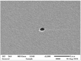
- FIG. 4 is a diagram showing pits; It is a figure which shows an example of the oxide semiconductor film of this invention.
- an oxide semiconductor film having few pits and excellent surface smoothness can be provided at low cost, and an oxide semiconductor film having few pits and excellent surface smoothness can be easily and inexpensively manufactured at a low temperature. It has been desired to provide a method for manufacturing an oxide semiconductor film formed by a process.
- an oxide semiconductor film containing gallium as a main component, the oxide semiconductor film having a corundum structure, and the oxide semiconductor film The oxide semiconductor film having 10,000/cm 2 or less pits on the surface of the film can be obtained easily and inexpensively, and has excellent surface smoothness, so that it can be suitably used for semiconductor devices.
- the inventors of the present invention have found a film forming method for forming a film by heat-treating a raw material solution that has been made into a mist, wherein the raw material solution is atomized or dropletized to generate a mist.
- a step of conveying the mist to a film forming section by a carrier gas a step of supplying the mist onto a substrate from a nozzle in the film forming section and performing heat treatment on the substrate to form a film;
- S [cm 2 ] is the area of the opening surface of the nozzle
- H [cm] is the longest distance between a point in the opening surface and the surface of the substrate
- H [cm] is supplied from the nozzle
- the oxide semiconductor film according to the present invention is characterized in that it contains gallium as a main component, has a corundum structure, and has pits of 10000/cm 2 or less.
- gallium is the main component of the metal.
- the main component here means that 50 to 100% of the metal component is gallium.
- Gallium-based means that it contains gallium as a metal component.
- Metal components other than gallium may include, for example, one or more metals selected from iron, indium, aluminum, vanadium, titanium, chromium, rhodium, iridium, nickel and cobalt.
- the number of pits is preferably less than 10000/cm 2 , more preferably 100/cm 2 or less, even more preferably less than 100/cm 2 .
- the lower limit of the pits is not particularly limited. It may be 0.01 pieces/cm 2 or more.
- the oxide semiconductor film can contain a dopant depending on the application.
- the dopant is not particularly limited. Examples include n-type dopants such as tin, germanium, silicon, titanium, zirconium, vanadium, or niobium, or p-type dopants such as copper, silver, tin, iridium, or rhodium.
- the dopant concentration may be, for example, about 1.0 ⁇ 10 16 to 1.0 ⁇ 10 22 /cm 3 , and even at a low concentration of about 1.0 ⁇ 10 17 /cm 3 or less, about 1.0 ⁇ 10 17 /cm 3 or less.
- the concentration may be as high as 0 ⁇ 10 20 /cm 3 or higher.
- the pits referred to in the present invention represent depressions formed on the film surface, as shown in FIG. 15, and can be observed with an optical microscope, SEM, TEM, or the like.
- the pit has an opening diameter of about 10 nm to 10 ⁇ m and a depth of 10 nm to 10 ⁇ m.
- the details of why the pits are generated are unknown, but when the mist has a large velocity component in the direction orthogonal to the substrate and the weight of the mist (moisture content) at the time of reaching the substrate is large, the mist collides with the substrate. It is conceivable that an excessive amount of raw material components is locally supplied due to an increase in the impulse at the time, and unreacted components and by-products in the mist remain on the film. Presumably, the presence of such residues on the film surface makes it difficult for the film to grow locally. Therefore, it is considered that the pit formation can be suppressed by reducing the velocity component of the mist in the direction perpendicular to the substrate and reducing the weight (moisture content) of the mist at the time of reaching the substrate under the conditions described later.
- the thickness of the oxide semiconductor film according to the present invention is not particularly limited. For example, it may be 0.05 to 100 ⁇ m, preferably 0.1 to 50 ⁇ m, more preferably 0.5 to 20 ⁇ m.
- An oxide semiconductor film 180 according to the present invention is formed on a substrate 181 as shown in FIG.
- the separate layer is a layer having a composition different from that of the substrate 181 and the oxide semiconductor film 180 of the outermost layer, and may be, for example, a crystalline oxide film, an insulating film, a metal film, or the like.
- the oxide semiconductor film preferably has an area of 10 cm 2 or more, and in the case of a circular shape, preferably has a diameter of 2 inches (50 mm) or more.
- the upper limit of the area is not particularly limited, it is preferably 750 cm 2 or less, and in the case of a circular shape, it is preferably 12 inches (300 mm) or less in diameter.
- the oxide semiconductor film according to the present invention can be used for semiconductor devices by appropriately designing the structure.
- semiconductor devices for example, Schottky barrier diode (SBD), metal semiconductor field effect transistor (MESFET), high electron mobility transistor (HEMT), metal oxide semiconductor field effect transistor (MOSFET), static induction transistor (SIT), junction field effect
- SBD Schottky barrier diode
- MESFET metal semiconductor field effect transistor
- HEMT high electron mobility transistor
- MOSFET metal oxide semiconductor field effect transistor
- SIT static induction transistor
- Each semiconductor layer can be composed of a transistor (JFET), an insulated gate bipolar transistor (IGBT), a light emitting diode (LED), or the like.
- FIG. 1 shows an example of a film forming apparatus 101 that can be used for the film forming method according to the present invention.
- the film forming apparatus 101 includes a mist forming unit 120 that forms mist from a raw material solution to generate mist, a carrier gas supply unit 130 that supplies a carrier gas for transporting the mist, and a heat treatment of the mist to form a film on a substrate. It has a film forming section 140 and a transfer section 109 that connects the misting section 120 and the film forming section 140 and transports the mist by a carrier gas. Further, the operation of the film forming apparatus 101 may be controlled by including a control unit (not shown) that controls the whole or part of the film forming apparatus 101 .
- the term "mist” as used in the present invention refers to a general term for fine particles of liquid dispersed in gas, and includes what is called mist, liquid droplets, and the like.
- the mist generating unit 120 mists the raw material solution to generate mist.
- the misting means is not particularly limited as long as it can mist the raw material solution, and may be a known misting means, but it is preferable to use a misting means using ultrasonic vibration. This is because mist can be made more stably.
- misting unit 120 may include a mist generation source 104 containing a raw material solution 104a, a container 105 containing a medium capable of transmitting ultrasonic vibrations, such as water 105a, and an ultrasonic transducer 106 attached to the bottom surface of the container 105.
- a mist generation source 104 which is a container containing a raw material solution 104a, is contained in a container 105 containing water 105a using a support (not shown).
- An ultrasonic transducer 106 is provided at the bottom of the container 105, and the ultrasonic transducer 106 and the oscillator 116 are connected. When the oscillator 116 is operated, the ultrasonic vibrator 106 vibrates, ultrasonic waves propagate through the water 105a into the mist generation source 104, and the raw material solution 104a turns into mist.
- the carrier gas supply unit 130 has a carrier gas source 102a that supplies carrier gas, and may include a flow control valve 103a for adjusting the flow rate of the carrier gas sent from the carrier gas source 102a.
- a carrier gas source 102b for dilution that supplies a carrier gas for dilution and a flow control valve 103b for adjusting the flow rate of the carrier gas for dilution sent out from the carrier gas source 102b for dilution can also be provided as necessary.
- the carrier gas may be supplied at two or more locations instead of at one location.
- the mist is heated and heat-treated to form a film on part or all of the surface of the substrate 110 .
- the film forming section 140 may be partially or wholly enclosed, or may not be enclosed.
- the film formation chamber 107 may surround the entire film formation unit 140 .
- a substrate 110 is installed in the film forming unit 140, and a hot plate 108 for heating the substrate 110 can be provided.
- the hot plate 108 may be provided inside the film forming chamber 107 as shown in FIG. 1 or may be provided outside the film forming chamber 107 .
- a moving stage 161a can be provided. Details will be described later.
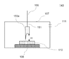
- the film forming section 140 is equipped with a nozzle 150 for supplying mist to the substrate 110, as shown in FIG.
- a nozzle 150 for supplying mist to the substrate 110
- FIG. 1 An example of nozzle 150 is shown in FIG.
- the nozzle 150 includes a connecting portion 151 that connects the conveying portion 109 and the nozzle 150, and a nozzle opening surface 152 for ejecting mist.
- the position where the nozzle 150 is installed is not particularly limited.
- the substrate 110 may be placed on the lower surface of the film formation chamber 107, and the nozzle 150 may be installed vertically above the substrate to form a face-up configuration.
- the nozzle 150 may be arranged face down, for example, vertically below the substrate.
- the number of nozzles and the number of opening surfaces of the nozzles are not particularly limited as long as they are one or more.
- a plurality of nozzles 150a and 150b may be provided as shown in FIG. 5, and a nozzle 150c may have a plurality of opening surfaces as shown in FIG.
- the angle formed by the plane including the nozzle opening surface 152 and the plane including the substrate 110 is not particularly limited.
- a nozzle 150d having a nozzle opening surface 152 that is inclined to facilitate the flow of mist in a specific direction may be provided, and as shown in FIG.
- the nozzle 150e may be provided with an inclination, it is preferable to provide the substrate 110 so that the opening surface of the nozzle is parallel to the substrate 110 as shown in FIG. This is because a film having a simpler structure, fewer pits, and excellent smoothness can be formed.
- the longest distance H [cm] between a point in the opening surface 152 of the nozzle and the surface of the substrate 110 can be appropriately adjusted within a range to be described later.
- a position adjustment mechanism (not shown) may be provided.
- the nozzle 150 may be assembled from a plurality of members, and the size of the members may be adjusted to appropriately adjust the area of the opening of the nozzle.
- the shape of the opening surface 152 of the nozzle is not particularly limited.
- a polygonal shape, a circular shape, an elliptical shape, etc. are conceivable, but a quadrangular shape is preferable, and a rectangular shape is more preferable.
- the film forming section 140 can be provided with a moving mechanism 160 for moving the substrate 110 below the nozzle 150 .
- the direction in which the substrate is moved is not particularly limited.
- FIGS. 10 and 11 show views of the film forming unit 140 having the moving mechanisms 160a and 160b as viewed from above the substrate 110 in the vertical direction.
- a moving stage 161a on which the substrate 110 and the hot plate 108 are placed is provided as shown in FIG. , the substrate 110 and the hot plate 108 are rotated under the nozzle 150 by a moving stage 161b on which the substrate 110 and the hot plate 108 are placed.
- a mechanism for rotating the substrate may be provided to rotate the substrate.
- the speed at which the substrate is moved and the range of movement are not particularly limited. .5 times or more is preferable, and 1 time or more is more preferable. If the number of times is 0.1 or more, there is no portion where the gas supplied locally is large (that is, the SH/Q does not decrease locally), so the number of pits does not increase and the smoothness of the surface is improved. Good film. Also, the upper limit of the number of times is not particularly limited, but if the number of times increases, the fixation of the substrate becomes unstable due to inertial force.
- v/D is 0.1/min, where v [mm/min] is the moving speed of the substrate with respect to the width D [mm] of moving the substrate. 0.5/min or more and 120/min or less is preferable, and 1 to 60/min is more preferable. D is not particularly limited, and is preferably equal to or larger than the diameter R [mm] of the substrate (100 mm or larger for 4 inches), and the upper limit is not particularly limited. If the size is increased, films can be formed on a large number of substrates per nozzle. However, since the film formation speed per substrate decreases, it is preferable to limit the number of substrates on which films are formed per nozzle to 1000 mm or less for excellent productivity.
- v is not particularly limited. It is preferably 10 mm/min or more and 30000 mm/min or less, preferably 30 mm/min or more and 12000 mm/min or less, and more preferably 60 mm/min or more and 6000 mm/min or less.
- the speed is preferably 0.1 rpm or more, preferably 0.5 to 120 rpm, more preferably 1 to 60 rpm.
- the exhaust port 111 for the exhaust gas may be provided at a position that does not affect the mist supply to the substrate 110 .
- the exhaust port 111 may be provided at one location or may be provided at two or more locations as long as it does not affect the supply of mist.
- the conveying section 109 connects the mist forming section 120 and the film forming section 140 . Mist is transported by the carrier gas from the mist generation source 104 of the mist generating unit 120 to the nozzle 150 of the film forming unit 140 via the transport unit 109 .
- the transport section 109 can be, for example, a supply pipe 109a.
- As the supply pipe 109a for example, a quartz pipe or a resin tube can be used.
- the present invention is a film forming method for forming a film by heat-treating a raw material solution that has been made into a mist, comprising: forming a film by atomizing or dropletizing the raw material solution to form a mist; and a step of supplying the mist onto a substrate from a nozzle in the film forming unit and performing heat treatment on the substrate to form a film, wherein the area of the opening surface of the nozzle is S [cm 2 ], H [cm] is the longest distance among distances between a point in the opening plane and the surface of the substrate, and Q [L/min] is the flow rate of the carrier gas supplied from the nozzle. , SH/Q ⁇ 0.015.
- the raw material solution 104a is atomized or dropletized to generate mist. This step can be performed using the misting unit 120 as described above.
- the raw material solution (aqueous solution) 104a is not particularly limited as long as it contains a material that can be misted, and may be an inorganic material or an organic material.
- a metal or metal compound solution is preferably used as the raw material solution, and contains one or more metals selected from gallium, iron, indium, aluminum, vanadium, titanium, chromium, rhodium, nickel and cobalt. can be used. Among these, those containing gallium are particularly preferable, and pits are suppressed, and a gallium-containing film having good smoothness can be formed.
- the raw material solution is not particularly limited as long as the solution of the metal (compound) can be misted, but as the raw material solution, the metal in the form of a complex or salt is dissolved or dispersed in an organic solvent or water. can be preferably used.
- forms of the complex include acetylacetonate complexes, carbonyl complexes, ammine complexes, hydride complexes, and the like.
- Salt forms include, for example, metal chloride salts, metal bromide salts, and metal iodide salts.
- a solution obtained by dissolving the above metal in hydrobromic acid, hydrochloric acid, hydroiodic acid, or the like can also be used as an aqueous salt solution.
- the solute concentration is preferably 0.01 to 1 mol/L. Among these, those containing halogen are particularly preferable, and pits are further suppressed, and a film having better smoothness can be formed.
- Additives such as hydrohalic acid and an oxidizing agent may be mixed in the raw material solution.
- the hydrohalic acid include hydrobromic acid, hydrochloric acid, hydroiodic acid, etc. Among them, hydrobromic acid and hydroiodic acid are preferable.
- the oxidizing agent include hydrogen peroxide (H 2 O 2 ), sodium peroxide (Na 2 O 2 ), barium peroxide (BaO 2 ), benzoyl peroxide (C 6 H 5 CO) 2 O 2 and the like. , hypochlorous acid (HClO), perchloric acid, nitric acid, ozone water, and organic peroxides such as peracetic acid and nitrobenzene.
- the raw material solution may contain a dopant.
- the dopant is not particularly limited. Examples include n-type dopants such as tin, germanium, silicon, titanium, zirconium, vanadium, or niobium, or p-type dopants such as copper, silver, tin, iridium, or rhodium.
- the dopant concentration may be, for example, about 1.0 ⁇ 10 ⁇ 9 to 1.0 mol/L, and even at a low concentration of about 1.0 ⁇ 10 ⁇ 7 mol/L or less, about 0.01 mol/L. /L or higher concentration.
- the generated mist is transported to the film forming section by a carrier gas.
- the type of carrier gas is not particularly limited, and can be appropriately selected according to the film to be deposited. Examples thereof include oxygen, ozone, inert gases such as nitrogen and argon, and reducing gases such as hydrogen gas and forming gas.
- the number of carrier gases may be one, or two or more.
- a diluent gas obtained by diluting the same gas as the first carrier gas with another gas (for example, diluted 10 times) may be further used as the second carrier gas, and air may also be used.
- the flow rate Q [L/min] of the carrier gas according to the present invention represents the total flow rate of the carrier gas.
- Q is the measured value at 20°C, and when measuring at other temperatures or measuring different types of flow rates (mass flow rate, etc.), convert to volumetric flow rate at 20°C using the equation of state of gas can do.
- the flow rate of the carrier gas (total flow rate when multiple types of gases are used) is not particularly limited as long as it satisfies the conditions described later.
- the flow rate is preferably 1 to 80 L/min, more preferably 4 to 40 L/min.
- Step of forming a film the mist is supplied from a nozzle onto the substrate, and heat treatment is performed on the substrate to form a film.
- the area of the nozzle opening surface 152 is S [cm 2 ]
- the flow rate of the carrier gas is Q [L/min]
- the longest distance between a point in the nozzle opening surface 152 and the surface between the substrates 110 is
- SH/Q should be 0.015 or more, preferably 0.1 or more and 20 or less.
- SH/Q is less than 0.015, the film has many pits and poor surface smoothness.
- the velocity of the carrier gas in the direction perpendicular to the substrate at the nozzle opening surface 152 is preferably 0.01 m/s or more and less than 8.0 m/s, preferably 0.1 m/s or more and 2.5 m/s. is less than
- the area S of the nozzle opening surface 152 is preferably 0.1 cm 2 or more and less than 400 cm 2 .
- the shortest distance H between the nozzle opening surface 152 and the substrate 110 is preferably 0.1 cm or more and 6.0 cm or less, more preferably 0.2 cm or more and 3.0 cm or less.
- the area of the nozzle opening surface 152 is S [cm 2 ] and the area of the substrate is A [cm 2 ], S/A ⁇ 0.3, more preferably 0.004 ⁇ S/A ⁇ 0. 15. If S/A ⁇ 0.3, the film has fewer pits and better surface smoothness.
- the area A of the substrate is preferably 10 cm 2 or more, and if the substrate is circular, it is preferably 2 inches (50 mm) or more in diameter. This is because a film with good surface smoothness can be formed over a larger area.
- the upper limit of A is not particularly limited. The larger the area of the substrate, the larger the area of the film that can be obtained in one film formation, which is suitable for mass production.
- L/R the long axis length of the nozzle opening surface 152
- R the maximum length of the substrate in the nozzle long axis direction
- L/R ⁇ 1 the long axis is the long side of the rectangle.
- the upper limit of L/R is not particularly limited, it is preferably 3 or less because the larger the L/R, the more mist is not supplied to the substrate.
- the heat treatment is not particularly limited as long as the mist reacts by heating. It can be appropriately set according to the raw material and the film-formed material.
- the heating temperature can be in the range of 120-600°C, preferably in the range of 200-600°C, more preferably in the range of 300-550°C.
- the heating temperature is T [°C]
- the area of the nozzle opening surface 152 is S [cm 2 ]
- the flow rate of the carrier gas is Q [L/min]
- ST/Q is preferably 40 or more, more preferably 100. 2000 or less. If ST/Q ⁇ 40, the film has fewer pits and a better surface smoothness.
- the heat treatment may be performed under vacuum, under a non-oxygen atmosphere, under a reducing gas atmosphere, under an air atmosphere, or under an oxygen atmosphere, and may be appropriately set according to the film to be deposited.
- the reaction pressure may be under atmospheric pressure, under increased pressure or under reduced pressure, but film formation under atmospheric pressure is preferable because the apparatus configuration can be simplified.
- the substrate 110 is not particularly limited as long as it can form a film and can support a film.
- the material of the substrate 110 is also not particularly limited, and a known substrate can be used, and it may be an organic compound or an inorganic compound.
- a known substrate can be used, and it may be an organic compound or an inorganic compound.
- Lithium oxide, lithium tantalate and the like are included, but not limited to these.
- the thickness of the substrate is not particularly limited, but preferably 10 to 2000 ⁇ m, more preferably 50 to 800 ⁇ m.
- Film formation may be performed directly on the substrate, or may be laminated on an intermediate layer formed on the substrate.
- the intermediate layer is not particularly limited, and can be composed mainly of, for example, an oxide containing any one of aluminum, titanium, vanadium, chromium, iron, gallium, rhodium, indium, and iridium.
- annealing may be performed after film formation.
- the temperature of the annealing treatment is not particularly limited, but is preferably 600° C. or lower, more preferably 550° C. or lower. This is because the crystallinity of the film is not impaired.
- the annealing treatment time is not particularly limited, but is preferably 10 seconds to 10 hours, more preferably 10 seconds to 1 hour.
- the substrate 110 may be separated from the oxide semiconductor film.
- the peeling means is not particularly limited, and known means may be used. Examples include means for applying mechanical impact to peel, means for applying heat and utilizing thermal stress for peeling, means for peeling by applying vibration such as ultrasonic waves, means for peeling by etching, and laser lift-off. be done. By the separation, the oxide semiconductor film can be obtained as a self-supporting film.
- Electrode A common method can be used to form the electrodes that are necessary to configure the semiconductor device. In other words, vapor deposition, sputtering, CVD, plating, etc., or a printing method for adhering together with resin or the like may be used.
- metal oxide conductive films such as tin oxide, zinc oxide, indium oxide, indium tin oxide (ITO), zinc indium oxide (IZO), organic conductive compounds such as polyaniline, polythiophene or polypyrrole, Any of them may be used, and an alloy or mixture of two or more of these may be used.
- the thickness of the electrode is preferably 1-1000 nm, more preferably 10-500 nm.
- the present invention is a film forming system for forming a film by heat-treating a raw material solution that has been turned into a mist, which includes a mechanism for atomizing or dropletizing the raw material solution to generate a mist, and a carrier gas for the mist to form a film.
- the area of the opening surface of the nozzle is S [cm 2 ]
- H [cm] is the longest distance among distances between a point in the opening plane and the surface of the substrate
- Q [L/min] is the flow rate of the carrier gas supplied from the nozzle.
- the raw material solution 104a is atomized or dropletized to generate mist. This mechanism can be performed using the misting unit 120 as described above.
- the raw material solution (aqueous solution) 104a is not particularly limited as long as it contains a material that can be misted, and may be an inorganic material or an organic material.
- a metal or metal compound solution is preferably used as the raw material solution, and contains one or more metals selected from gallium, iron, indium, aluminum, vanadium, titanium, chromium, rhodium, nickel and cobalt. can be used. Among these, those containing gallium are particularly preferable, and pits are suppressed, and a gallium-containing film having good smoothness can be formed.
- the raw material solution is not particularly limited as long as the solution of the metal (compound) can be misted, but as the raw material solution, the metal in the form of a complex or salt is dissolved or dispersed in an organic solvent or water. can be preferably used.
- forms of the complex include acetylacetonate complexes, carbonyl complexes, ammine complexes, hydride complexes, and the like.
- Salt forms include, for example, metal chloride salts, metal bromide salts, and metal iodide salts.
- a solution obtained by dissolving the above metal in hydrobromic acid, hydrochloric acid, hydroiodic acid, or the like can also be used as an aqueous salt solution.
- the solute concentration is preferably 0.01 to 1 mol/L. Among these, those containing halogen are particularly preferable, and pits are further suppressed, and a film having better smoothness can be formed.
- Additives such as hydrohalic acid and an oxidizing agent may be mixed in the raw material solution.
- the hydrohalic acid include hydrobromic acid, hydrochloric acid, hydroiodic acid, etc. Among them, hydrobromic acid and hydroiodic acid are preferable.
- the oxidizing agent include hydrogen peroxide (H 2 O 2 ), sodium peroxide (Na 2 O 2 ), barium peroxide (BaO 2 ), benzoyl peroxide (C 6 H 5 CO) 2 O 2 and the like. , hypochlorous acid (HClO), perchloric acid, nitric acid, ozone water, and organic peroxides such as peracetic acid and nitrobenzene.
- the raw material solution may contain a dopant.
- the dopant is not particularly limited. Examples include n-type dopants such as tin, germanium, silicon, titanium, zirconium, vanadium, or niobium, or p-type dopants such as copper, silver, tin, iridium, or rhodium.
- the dopant concentration may be, for example, about 1.0 ⁇ 10 ⁇ 9 to 1.0 mol/L, and even at a low concentration of about 1.0 ⁇ 10 ⁇ 7 mol/L or less, about 0.01 mol/L. /L or higher concentration.
- the generated mist is transported to the film forming section by a carrier gas.
- This mechanism can be performed using the transport section 109 as described above.
- the type of carrier gas is not particularly limited, and can be appropriately selected according to the film to be deposited. Examples thereof include oxygen, ozone, inert gases such as nitrogen and argon, and reducing gases such as hydrogen gas and forming gas.
- the number of carrier gases may be one, or two or more. For example, a diluent gas obtained by diluting the same gas as the first carrier gas with another gas (for example, diluted 10 times) may be further used as the second carrier gas, and air may also be used.
- the flow rate Q [L/min] of the carrier gas according to the present invention represents the total flow rate of the carrier gas.
- Q is the measured value at 20°C, and when measuring at other temperatures or measuring different types of flow rates (mass flow rate, etc.), convert to volumetric flow rate at 20°C using the equation of state of gas can do.
- the flow rate of the carrier gas (total flow rate when multiple types of gases are used) is not particularly limited as long as it satisfies the conditions described later.
- the flow rate is preferably 1 to 80 L/min, more preferably 4 to 40 L/min.
- the mist is supplied from a nozzle onto the substrate, and heat treatment is performed on the substrate to form a film.
- the area of the nozzle opening surface 152 is S [cm 2 ]
- the flow rate of the carrier gas is Q [L/min]
- the longest distance between a point in the nozzle opening surface 152 and the surface between the substrates 110 is
- SH/Q should be 0.015 or more, preferably 0.1 or more and 20 or less.
- SH/Q is less than 0.015, the film has many pits and poor surface smoothness.
- the velocity of the carrier gas in the direction perpendicular to the substrate at the nozzle opening surface 152 is preferably 0.01 m/s or more and less than 8.0 m/s, preferably 0.1 m/s or more and 2.5 m/s. is less than
- the area S of the nozzle opening surface 152 is preferably 0.1 cm 2 or more and less than 400 cm 2 .
- the shortest distance H between the nozzle opening surface 152 and the substrate 110 is preferably 0.1 cm or more and 6.0 cm or less, more preferably 0.2 cm or more and 3.0 cm or less.
- the area of the nozzle opening surface 152 is S [cm 2 ] and the area of the substrate is A [cm 2 ], S/A ⁇ 0.3, more preferably 0.004 ⁇ S/A ⁇ 0. 15. If S/A ⁇ 0.3, the film has fewer pits and better surface smoothness.
- the area A of the substrate is preferably 10 cm 2 or more, and if the substrate is circular, it is preferably 2 inches (50 mm) or more in diameter. This is because a film with good surface smoothness can be formed over a larger area.
- the upper limit of A is not particularly limited. The larger the area of the substrate, the larger the area of the film that can be obtained in one film formation, which is suitable for mass production.
- L/R the long axis length of the nozzle opening surface 152
- R the maximum length of the substrate in the nozzle long axis direction
- L/R ⁇ 1 the long axis is the long side of the rectangle.
- the upper limit of L/R is not particularly limited, it is preferably 3 or less because the larger the L/R, the more mist is not supplied to the substrate.
- the heat treatment is not particularly limited as long as the mist reacts by heating. It can be appropriately set according to the raw material and the film-formed material.
- the heating temperature can be in the range of 120-600°C, preferably in the range of 200-600°C, more preferably in the range of 300-550°C.
- the heating temperature is T [°C]
- the area of the nozzle opening surface 152 is S [cm 2 ]
- the flow rate of the carrier gas is Q [L/min]
- ST/Q is preferably 40 or more, more preferably 100. 2000 or less. If ST/Q ⁇ 40, the film has fewer pits and a better surface smoothness.
- the heat treatment may be performed under vacuum, under a non-oxygen atmosphere, under a reducing gas atmosphere, under an air atmosphere, or under an oxygen atmosphere, and may be appropriately set according to the film to be deposited.
- the reaction pressure may be under atmospheric pressure, under increased pressure or under reduced pressure, but film formation under atmospheric pressure is preferable because the apparatus configuration can be simplified.
- the substrate 110 is not particularly limited as long as it can form a film and can support a film.
- the material of the substrate 110 is also not particularly limited, and a known substrate can be used, and it may be an organic compound or an inorganic compound.
- a known substrate can be used, and it may be an organic compound or an inorganic compound.
- Lithium oxide, lithium tantalate and the like are included, but not limited to these.
- the thickness of the substrate is not particularly limited, but preferably 10 to 2000 ⁇ m, more preferably 50 to 800 ⁇ m.
- Film formation may be performed directly on the substrate, or may be laminated on an intermediate layer formed on the substrate.
- the intermediate layer is not particularly limited, and can be composed mainly of, for example, an oxide containing any one of aluminum, titanium, vanadium, chromium, iron, gallium, rhodium, indium, and iridium.
- annealing may be performed after film formation.
- the temperature of the annealing treatment is not particularly limited, but is preferably 600° C. or lower, more preferably 550° C. or lower. This is because the crystallinity of the film is not impaired.
- the annealing treatment time is not particularly limited, but is preferably 10 seconds to 10 hours, more preferably 10 seconds to 1 hour.
- the substrate 110 may be separated from the oxide semiconductor film.
- the peeling means is not particularly limited, and known means may be used. Examples include means for applying mechanical impact to peel, means for applying heat and utilizing thermal stress for peeling, means for peeling by applying vibration such as ultrasonic waves, means for peeling by etching, and laser lift-off. be done. By the separation, the oxide semiconductor film can be obtained as a self-supporting film.
- Electrode A common method can be used to form the electrodes that are necessary to configure the semiconductor device. In other words, vapor deposition, sputtering, CVD, plating, etc., or a printing method for adhering together with resin or the like may be used.
- metal oxide conductive films such as tin oxide, zinc oxide, indium oxide, indium tin oxide (ITO), zinc indium oxide (IZO), organic conductive compounds such as polyaniline, polythiophene or polypyrrole, Any of them may be used, and an alloy or mixture of two or more of these may be used.
- the thickness of the electrode is preferably 1-1000 nm, more preferably 10-500 nm.
- Example 1 a film forming apparatus as shown in FIG. 1 was used.
- a 0.05 mol/L gallium iodide aqueous solution was mixed with tin chloride to prepare an aqueous solution so that the atomic ratio of tin to gallium was 1:0.08, and this was used as a raw material solution 104a.
- the raw material solution 104 a obtained as described above was accommodated in the mist generation source 104 .
- the temperature of the solution at this time was 25°C.
- a 4-inch (100 mm diameter) c-plane sapphire substrate as substrate 110 was placed on hot plate 108 in deposition chamber 107, and hot plate 108 was operated to raise the temperature to 500.degree.
- the flow control valves 103a and 103b are opened to supply nitrogen gas as a carrier gas from the carrier gas sources 102a and 102b into the film forming chamber 107 to sufficiently replace the atmosphere in the film forming chamber 107 with the carrier gas,
- the flow rate of the main carrier gas was adjusted to 12 L/min, and the flow rate of the diluent carrier gas was adjusted to 12 L/min.
- the ultrasonic vibrator 106 was oscillated at 2.4 MHz, and the vibration was propagated to the raw material solution 104a through the water 105a, thereby misting the raw material solution 104a to generate mist. This mist was supplied to the substrate 110 through the supply pipe 109a and the nozzle 150 by carrier gas.
- Example 5 The concentration of the raw material solution is 0.3 mol/L, the area S of the nozzle opening surface is 1.2 cm 2 , and the longest distance H among the distances between a point in the nozzle opening surface 152 and the surface of the substrate 110 is 2.
- Test example 1 The film surface after film formation was observed with an optical microscope, and the number of pits within 0.01 to 1 cm 2 was counted. Table 1 shows the density of pits calculated by dividing the count number of pits by the observed area. FIG. 12 shows the result of plotting the pit density against SH/Q.
- Test example 2 Using the semiconductor film obtained as described above, a semiconductor device 170 as shown in FIG. 13 was fabricated.
- a Pt layer, a Ti layer, and an Au layer were deposited on the n-type semiconductor layer 171a by electron beam evaporation to form a Schottky electrode 172. As shown in FIG.
- An ohmic electrode 173 was formed by stacking a Ti layer and an Au layer on the n + -type semiconductor layer 171b by electron beam evaporation.
- the present invention is not limited to the above embodiments.
- the above-described embodiment is an example, and any device having substantially the same configuration as the technical idea described in the claims of the present invention and exhibiting the same effect is the present invention. included in the technical scope of
Landscapes
- Chemical & Material Sciences (AREA)
- Organic Chemistry (AREA)
- Metallurgy (AREA)
- Chemical Kinetics & Catalysis (AREA)
- Engineering & Computer Science (AREA)
- Materials Engineering (AREA)
- Mechanical Engineering (AREA)
- General Chemical & Material Sciences (AREA)
- Inorganic Chemistry (AREA)
- Dispersion Chemistry (AREA)
- Crystals, And After-Treatments Of Crystals (AREA)
- Liquid Deposition Of Substances Of Which Semiconductor Devices Are Composed (AREA)
- Formation Of Insulating Films (AREA)
- Chemical Vapour Deposition (AREA)
- Crystallography & Structural Chemistry (AREA)
- Insulated Gate Type Field-Effect Transistor (AREA)
Abstract
Description
本発明は、上記問題を解決するためになされたものであり、ピットを抑制し、表面の平滑性が良好な膜、および、そのような膜を成膜する成膜方法を提供することを目的とする。
前記原料溶液を霧化または液滴化してミストを生成する工程と、
前記ミストをキャリアガスにより成膜部に搬送する工程と、
前記成膜部においてノズルから前記ミストを基板上へ供給して前記基板上にて熱処理して成膜を行う工程と、
を含み、
前記ノズルの開口面の面積をS[cm2]、前記開口面内の点と前記基板の表面との距離の中で最長となる距離をH[cm]、前記ノズルから供給される前記キャリアガスの流量をQ[L/分]としたとき、SH/Q≧0.015とする、
成膜方法を提供する。
また、本発明の成膜方法によれば、ミストCVD法において、簡便な方法により、表面のピットが少なく、平滑性が良好な膜を成膜することが可能となる。
本発明に係る酸化物半導体膜は、ガリウムを主成分とし、コランダム構造であって、ピットが10000個/cm2以下である点に特徴を有している。一般に酸化物半導体膜は金属と酸素から構成されるが、本発明に係る酸化物半導体膜においては、金属はガリウムを主成分とするものである。ここでいう主成分とは、金属成分のうち、50~100%がガリウムであることを意味する。またガリウム系とは、金属成分としてガリウムを含んでいるものであることを意味する。ガリウム以外の金属成分としては、例えば、鉄、インジウム、アルミニウム、バナジウム、チタン、クロム、ロジウム、イリジウム、ニッケル及びコバルトから選ばれる1種又は2種以上の金属を含んでもよい。
図1に、本発明に係る成膜方法に使用可能な成膜装置101の一例を示す。成膜装置101は、原料溶液をミスト化してミストを発生させるミスト化部120と、ミストを搬送するキャリアガスを供給するキャリアガス供給部130と、ミストを熱処理して基板上に成膜を行う成膜部140と、ミスト化部120と成膜部140とを接続し、キャリアガスによってミストが搬送される搬送部109とを有する。また、成膜装置101は、成膜装置101の全体又は一部を制御する制御部(図示なし)を備えることによって、その動作が制御されてもよい。
ここで、本発明でいうミストとは、気体中に分散した液体の微粒子の総称を指し、霧、液滴等と呼ばれるものも含む。
ミスト化部120では、原料溶液をミスト化してミストを発生させる。ミスト化手段は、原料溶液をミスト化できさえすれば特に限定されず、公知のミスト化手段であってもよいが、超音波振動によるミスト化手段を用いることが好ましい。より安定してミスト化することができるためである。
キャリアガス供給部130は、キャリアガスを供給するキャリアガス源102aを有し、キャリアガス源102aから送り出されるキャリアガスの流量を調節するための流量調節弁103aを備えていてもよい。また、必要に応じて希釈用キャリアガスを供給する希釈用キャリアガス源102bや、希釈用キャリアガス源102bから送り出される希釈用キャリアガスの流量を調節するための流量調節弁103bを備えることもできる。また、キャリアガスの供給箇所も1箇所だけでなく、2箇所以上あってもよい。
成膜部140では、ミストを加熱し熱処理させて、基板110の表面の一部又は全部に成膜を行う。成膜部140は、成膜部140の一部または全体が囲われていてもよく、囲われていなくてもよい。例えば、図1に示すように、成膜部140の全体を囲い、成膜室107としてもよい。成膜部140には、基板110が設置されており、該基板110を加熱するためのホットプレート108を備えることができる。ホットプレート108は、図1に示されるように成膜室107の内部に設けられていてもよいし、成膜室107の外部に設けられていてもよい。また、移動ステージ161aを備えることができる。詳細については後述する。
また、ノズル150を複数の部材より組み立てる構造とし、部材のサイズ調整により、ノズルの開口面の面積を適宜調整できる構造としてもよい。
搬送部109は、ミスト化部120と成膜部140とを接続する。搬送部109を介して、ミスト化部120のミスト発生源104から成膜部140のノズル150へと、キャリアガスによってミストが搬送される。搬送部109は、例えば、供給管109aとすることができる。供給管109aとしては、例えば石英管や樹脂製のチューブなどを使用することができる。
次に、本発明に係る成膜方法について説明する。本発明は、ミスト化した原料溶液を熱処理して成膜を行う成膜方法であって、前記原料溶液を霧化または液滴化してミストを生成する工程と、前記ミストをキャリアガスにより成膜部に搬送する工程と、前記成膜部においてノズルから前記ミストを基板上へ供給して前記基板上にて熱処理して成膜を行う工程と、を含み、前記ノズルの開口面の面積をS[cm2]、前記開口面内の点と前記基板の表面との距離の中で最長となる距離をH[cm]、前記ノズルから供給される前記キャリアガスの流量をQ[L/分]としたとき、SH/Q≧0.015とする成膜方法である。
まず、原料溶液104aを霧化または液滴化してミストを生成する。この工程は上述のようなミスト化部120を用いて行うことができる。ここで原料溶液(水溶液)104aは、ミスト化が可能な材料を含んでいれば特に限定されず、無機材料であっても、有機材料であってもよい。原料溶液には、金属又は金属化合物の溶液が好適に用いられ、ガリウム、鉄、インジウム、アルミニウム、バナジウム、チタン、クロム、ロジウム、ニッケル及びコバルトから選ばれる1種又は2種以上の金属を含むものを使用できる。これらの中でも特にガリウムを含むものが好ましく、ピットが抑制され、平滑性が良好なガリウム含有膜が成膜できる。
次に、生成したミストをキャリアガスにより成膜部に搬送する。ここでキャリアガスの種類は、特に限定されず、成膜物に応じて適宜選択可能である。例えば、酸素、オゾン、窒素やアルゴン等の不活性ガス、又は水素ガスやフォーミングガス等の還元ガスなどが挙げられる。また、キャリアガスの種類は1種類でも、2種類以上であってもよい。例えば、第1のキャリアガスと同じガスをそれ以外のガスで希釈した(例えば10倍に希釈した)希釈ガスなどを、第2のキャリアガスとしてさらに用いてもよく、空気を用いることもできる。
次に、成膜部においてノズルから前記ミストを基板上へ供給して前記基板上にて熱処理して成膜を行う。ここでノズルの開口面152の面積をS[cm2]、キャリアガスの流量をQ[L/分]、前記ノズルの開口面152内の点と基板110間の表面との距離の中で最長となる距離をH[cm]としたとき、SH/Qが0.015以上であれば良く、好ましくは、0.1以上20以下である。SH/Qが0.015未満であると、ピットが多く、表面の平滑性が悪い膜となる。また、このときノズルの開口面152における基板と直交する方向のキャリアガスの速度は、0.01m/s以上8.0m/s未満がよく、好ましくは0.1m/s以上2.5m/s未満である。
基板110を酸化物半導体膜から剥離してもよい。剥離手段は特に限定されず、公知の手段であってもよい。例えば、機械的衝撃を与えて剥離する手段、熱を加えて熱応力を利用して剥離する手段、超音波等の振動を加えて剥離する手段、エッチングして剥離する手段、レーザーリフトオフなどが挙げられる。前記剥離によって、酸化物半導体膜を自立膜として得ることができる。
半導体装置を構成するために必要となる電極の形成は、一般的な方法を用いることができる。すなわち、蒸着、スパッタ、CVD、めっきなどの他、樹脂等と一緒に接着させる印刷法など、いずれを用いてもかまわない。電極材料としては、Al、Ag、Ti、Pd、Au、Cu、Cr、Fe、W、Ta、Nb、Mn、Mo、Hf、Co、Zr、Sn、Pt、V、Ni、Ir、Zn、In、Ndなどの金属の他、酸化スズ、酸化亜鉛、酸化インジウム、酸化インジウムスズ(ITO)、酸化亜鉛インジウム(IZO)等の金属酸化物導電膜、ポリアニリン、ポリチオフェンまたはポリピロールなどの有機導電性化合物、いずれを用いてもかまわないし、これらの2種以上の合金、混合物でもかまわない。電極の厚さは、1~1000nmが好ましく、より好ましくは10~500nmである。
次に、本発明に係る成膜システムについて説明する。本発明は、ミスト化した原料溶液を熱処理して成膜を行う成膜システムであって、前記原料溶液を霧化または液滴化してミストを生成する機構と、前記ミストをキャリアガスにより成膜部に搬送する機構と、前記成膜部においてノズルから前記ミストを基板上へ供給して前記基板上にて熱処理して成膜を行う機構と、を含み、前記ノズルの開口面の面積をS[cm2]、前記開口面内の点と前記基板の表面との距離の中で最長となる距離をH[cm]、前記ノズルから供給される前記キャリアガスの流量をQ[L/分]としたとき、SH/Q≧0.015とする成膜システムである。
まず、原料溶液104aを霧化または液滴化してミストを生成する。この機構は上述のようなミスト化部120を用いて行うことができる。ここで原料溶液(水溶液)104aは、ミスト化が可能な材料を含んでいれば特に限定されず、無機材料であっても、有機材料であってもよい。原料溶液には、金属又は金属化合物の溶液が好適に用いられ、ガリウム、鉄、インジウム、アルミニウム、バナジウム、チタン、クロム、ロジウム、ニッケル及びコバルトから選ばれる1種又は2種以上の金属を含むものを使用できる。これらの中でも特にガリウムを含むものが好ましく、ピットが抑制され、平滑性が良好なガリウム含有膜が成膜できる。
次に、生成したミストをキャリアガスにより成膜部に搬送する。この機構は上述のような搬送部109を用いて行うことができる。ここでキャリアガスの種類は、特に限定されず、成膜物に応じて適宜選択可能である。例えば、酸素、オゾン、窒素やアルゴン等の不活性ガス、又は水素ガスやフォーミングガス等の還元ガスなどが挙げられる。また、キャリアガスの種類は1種類でも、2種類以上であってもよい。例えば、第1のキャリアガスと同じガスをそれ以外のガスで希釈した(例えば10倍に希釈した)希釈ガスなどを、第2のキャリアガスとしてさらに用いてもよく、空気を用いることもできる。
次に、成膜部140においてノズルから前記ミストを基板上へ供給して前記基板上にて熱処理して成膜を行う。ここでノズルの開口面152の面積をS[cm2]、キャリアガスの流量をQ[L/分]、前記ノズルの開口面152内の点と基板110間の表面との距離の中で最長となる距離をH[cm]としたとき、SH/Qが0.015以上であれば良く、好ましくは、0.1以上20以下である。SH/Qが0.015未満であると、ピットが多く、表面の平滑性が悪い膜となる。また、このときノズルの開口面152における基板と直交する方向のキャリアガスの速度は、0.01m/s以上8.0m/s未満がよく、好ましくは0.1m/s以上2.5m/s未満である。
基板110を酸化物半導体膜から剥離してもよい。剥離手段は特に限定されず、公知の手段であってもよい。例えば、機械的衝撃を与えて剥離する手段、熱を加えて熱応力を利用して剥離する手段、超音波等の振動を加えて剥離する手段、エッチングして剥離する手段、レーザーリフトオフなどが挙げられる。前記剥離によって、酸化物半導体膜を自立膜として得ることができる。
半導体装置を構成するために必要となる電極の形成は、一般的な方法を用いることができる。すなわち、蒸着、スパッタ、CVD、めっきなどの他、樹脂等と一緒に接着させる印刷法など、いずれを用いてもかまわない。電極材料としては、Al、Ag、Ti、Pd、Au、Cu、Cr、Fe、W、Ta、Nb、Mn、Mo、Hf、Co、Zr、Sn、Pt、V、Ni、Ir、Zn、In、Ndなどの金属の他、酸化スズ、酸化亜鉛、酸化インジウム、酸化インジウムスズ(ITO)、酸化亜鉛インジウム(IZO)等の金属酸化物導電膜、ポリアニリン、ポリチオフェンまたはポリピロールなどの有機導電性化合物、いずれを用いてもかまわないし、これらの2種以上の合金、混合物でもかまわない。電極の厚さは、1~1000nmが好ましく、より好ましくは10~500nmである。
本実施例では、図1に示すような成膜装置を用いた。
0.05mol/Lヨウ化ガリウム水溶液に塩化スズを混合し、ガリウムに対するスズの原子比が1:0.08となるように水溶液を調製し、これを原料溶液104aとした。上述のようにして得た原料溶液104aをミスト発生源104内に収容した。このときの溶液の温度は25℃であった。
次に、基板110として4インチ(直径100mm)のc面サファイア基板を、成膜室107内でホットプレート108に載置し、ホットプレート108を作動させて温度を500℃に昇温した。
続いて、流量調節弁103a、103bを開いてキャリアガス源102a、102bからキャリアガスとして窒素ガスを成膜室107内に供給し、成膜室107の雰囲気をキャリアガスで十分に置換するとともに、主キャリアガスの流量を12L/分に、希釈用キャリアガスの流量を12L/分にそれぞれ調節した。
次に、超音波振動子106を2.4MHzで振動させ、その振動を、水105aを通じて原料溶液104aに伝播させることによって、原料溶液104aをミスト化してミストを生成した。
このミストを、キャリアガスによって供給管109a、ノズル150を経て、基板110に供給した。ノズル150としては、ノズルの開口面152が長方形形状のノズルを用い、ノズルの開口面152の面積をS[cm2]、キャリアガスの流量をQ[L/分]、ノズルの開口面152内の点と基板110の表面との距離の中で最長となる距離をH[cm]としたとき、SH/Q=0.5になるように調整した。このとき、S=6.0、H=2.0、Q=24である。
そして、大気圧下、500℃の条件で、成膜室107内でミストを熱処理させて、基板110上にコランダム構造を有する酸化ガリウム(α-Ga2O3)の薄膜を形成した。成膜時間は30分とした。
熱処理温度T[℃]としたとき、ST/Q=40、基板の面積をA[cm2]としたとき、S/A=0.024、ノズルの開口面152の長軸長さをL[cm]、基板のノズル長軸方向の最大長さR[cm]としたとき、L/R=1.2であった。このとき、T=500、A=78.5、L=12、R=10である。
基板は図10のような移動機構により、基板およびホットプレートを15cm/分の速度で、1分間に一度ノズルの下を通過するように往復移動させた。
続いて、上記の様にして得たn+半導体膜上に、2層目として、塩化スズを含まないこと以外上記と同様の原料溶液を用い、同様の条件にてn-半導体膜を積層した。
ノズルの開口面の面積Sを10.8cm2、キャリアガスの総流量を計40L/分、成膜温度Tを550℃に変更したこと以外は、実施例1と同様に成膜を行った。このとき、SH/Q=0.54、ST/Q=149、S/A=0.15であった。
キャリアガスの総流量を計20L/分、成膜温度Tを500℃に変更したこと以外は、実施例2と同様に成膜を行った。このとき、SH/Q=1.08、ST/Q=270、S/A=0.15であった。
成膜温度Tを500℃に変更したこと以外は、実施例2と同様に成膜を行った。このとき、SH/Q=0.54、ST/Q=135、S/A=0.15であった。
原料溶液の濃度を0.3mol/L、ノズルの開口面の面積Sを1.2cm2、ノズルの開口面152内の点と基板110の表面との距離の中で最長となる距離Hを2.5cm、キャリアガスの総流量を計14L/分に変更したこと以外は、実施例1と同様に成膜を行った。このとき、SH/Q=0.21、ST/Q=42.9、S/A=0.015であった。
原料溶液を0.3mol/Lの臭化ガリウム水溶液とし、ノズルの開口面152内の点と基板110の表面との距離の中で最長となる距離Hを1.6cmに変更したこと以外は、実施例5と同様に成膜を行った。このとき、SH/Q=0.14、ST/Q=42.9、S/A=0.015であった。
6インチ(直径150mm)のサファイア基板を基板110として用いたこと、ノズルの開口面の面積Sを8.5cm2、ノズルの開口面152内の点と基板110の表面との距離の中で最長となる距離Hを0.2cm、キャリアガスの総流量を計36L/分に変更したこと以外は、実施例1と同様に成膜を行った。このとき、SH/Q=0.047、ST/Q=118、S/A=0.048、L/R=1.1であった。
原料溶液としてガリウムアセチルアセトナート錯体を1.5体積%の塩酸を含む水に溶解させた0.05mol/Lの水溶液を用いたこと、ノズルの開口面の面積Sを1.2cm2、ノズルの開口面152内の点と基板110の表面との距離の中で最長となる距離Hを0.2cm、キャリアガスの総流量を計10L/分、成膜温度Tを450℃に変更したこと以外は、実施例1と同様に成膜を行った。このとき、SH/Q=0.024、ST/Q=54、S/A=0.015であった。
ノズルの開口面152内の点と基板110の表面との距離の中で最長となる距離Hを1.2cmに変更したこと以外は、実施例6と同様に成膜を行った。このとき、SH/Q=0.1、ST/Q=42.9、S/A=0.015であった。
ノズルの開口面の面積Sを24cm2、ノズルの開口面152内の点と基板110の表面との距離の中で最長となる距離Hを0.2cm、キャリアガスの総流量を計80L/分、成膜温度Tを550℃に変更したこと以外は、実施例1と同様に成膜を行った。このとき、SH/Q=0.06、ST/Q=165、S/A=0.30であった。
ノズルの開口面の面積Sを5.0cm2、ノズルの開口面152内の点と基板110の表面との距離の中で最長となる距離Hを0.2cm、キャリアガスの総流量を計60L/分、実施例1と同様に成膜を行った。このとき、SH/Q=0.017、ST/Q=41.7、S/A=0.064、L/R=1.0であった。
ノズルの開口面の形状を直径4インチ(100mm)の円形としたこと、ノズルの開口面152内の点と基板110の表面との距離の中で最長となる距離Hを0.2cmに変更したこと、基板を移動させなかったこと、キャリアガスの流量を計80L/分に変更し、加熱温度を550℃としたこと以外は、実施例1と同様に成膜を行った。このとき、SH/Q=0.20、ST/Q=540、S/A=1、L/R=1であった。
原料溶液を0.05mol/Lの臭化ガリウム水溶液とし、臭化重水素酸を体積比で10%を添加させたこと、ノズルの開口面152内の点と基板110の表面との距離の中で最長となる距離Hを0.2cm、成膜温度Tを470℃に変更したこと以外は、実施例6と同様に成膜を行った。このとき、SH/Q=0.017、ST/Q=40、S/A=0.015であった。
原料溶液を0.05mol/Lのヨウ化ガリウム水溶液とし、ノズルの開口面152内の点と基板110の表面との距離の中で最長となる距離Hを0.2cm、キャリアガスの総流量を計16L/分、成膜温度Tを450℃に変更したこと以外は、実施例6と同様に成膜を行った。このとき、SH/Q=0.015、ST/Q=33.8、S/A=0.015であった。
キャリアガスの総流量を計20L/分に変更したこと以外は、実施例14と同様に成膜を行った。このとき、SH/Q=0.012、ST/Q=27、S/A=0.015であった。
キャリアガスの総流量を計24L/分に変更したこと以外は、実施例14と同様に成膜を行った。このとき、SH/Q=0.01、ST/Q=22.5、S/A=0.015であった。
キャリアガスの総流量を計48L/分に変更したこと以外は、実施例14と同様に成膜を行った。このとき、SH/Q=0.005、ST/Q=11.3、S/A=0.015であった。
キャリアガスの総流量を計60L/分に変更したこと以外は、実施例14と同様に成膜を行った。このとき、SH/Q=0.004、ST/Q=9、S/A=0.015であった。
成膜後の膜表面を光学顕微鏡により観察し、0.01~1cm2内にあるピットの数をカウントした。ピット箇所のカウント数を観察面積で割ることで算出したピットの密度を表1に示した。また、SH/Qに対し、ピット密度をプロットした結果を図12に示す。
上記の様にして得た半導体膜を用い、図13の様な半導体装置170を作成した。
n-型半導体層171a上に、Pt層、Ti層およびAu層をそれぞれ電子ビーム蒸着にて積層し、ショットキー電極172を形成した。
n+型半導体層171b上に、Ti層およびAu層をそれぞれ電子ビーム蒸着にて積層し、オーミック電極173を形成した。
得られた半導体装置につき、電流電圧特性を評価した。逆方向の電流電圧特性の測定により、絶縁破壊が起こる電圧を調べた。耐圧300V以上の半導体装置を合格品とし、合格品数/半導体装置作成総数=歩留[%]として、歩留を算出した。結果を表1に示す。
また、試験例1で算出したピット密度に対して、歩留をプロットした図を図14に示す。

Claims (15)
- ガリウムを主成分とする酸化物半導体膜であって、
前記酸化物半導体膜がコランダム構造を有するものであって、
該酸化物半導体膜の表面のピットが10000個/cm2以下のものである、
ことを特徴とする酸化物半導体膜。 - 前記酸化物半導体膜の表面の前記ピットが100個/cm2以下のものである、
ことを特徴とする請求項1に記載の酸化物半導体膜。 - 前記酸化物半導体膜の面積が10cm2以上のものである、
ことを特徴とする請求項1又は請求項2に記載の酸化物半導体膜。 - 前記酸化物半導体膜の表面の前記ピットが開口径10nm~10μm、深さ10nm~10μmのものである、
ことを特徴とする請求項1から請求項3のいずれか1項に記載の酸化物半導体膜。 - 請求項1から請求項4のいずれか1項に記載の酸化物半導体膜を含むものであることを特徴とする半導体装置。
- ミスト化した原料溶液を熱処理して成膜を行う成膜方法であって、
前記原料溶液を霧化または液滴化してミストを生成する工程と、
前記ミストをキャリアガスにより成膜部に搬送する工程と、
前記成膜部においてノズルから前記ミストを基板上へ供給して前記基板上にて熱処理して成膜を行う工程と、
を含み、
前記ノズルの開口面の面積をS[cm2]、前記開口面内の点と前記基板の表面との距離の中で最長となる距離をH[cm]、前記ノズルから供給される前記キャリアガスの流量をQ[L/分]としたとき、SH/Q≧0.015とする、
ことを特徴とする成膜方法。 - 前記原料溶液がガリウムを含むことを特徴とする請求項6に記載の成膜方法。
- 前記原料溶液がハロゲンを含むことを特徴とする請求項6または請求項7に記載の成膜方法。
- 前記熱処理の温度をT[℃]としたとき、ST/Q≧40とすることを特徴とする請求項6から請求項8のいずれか1項に記載の成膜方法。
- 前記基板上への前記ミストの供給を前記基板の鉛直上方に備えられた前記ノズルより行うことを特徴とする請求項6から請求項9のいずれか1項に記載の成膜方法。
- 前記基板を前記ノズルの下で移動させることを特徴とする請求項10に記載の成膜方法。
- 前記基板の成膜される表面の面積をA[cm2]としたとき、S/A≦0.3とすることを特徴とする請求項11に記載の成膜方法。
- 前記ノズルの開口面が長方形であることを特徴とする請求項6から請求項12のいずれか1項に記載の成膜方法。
- 前記ノズルの開口面の長軸長さをL[cm]、前記基板の成膜される表面内の、ノズル長軸方向の最大長さをR[cm]としたとき、L/R≧1とすることを特徴とする請求項13に記載の成膜方法。
- 前記基板の面積が10cm2以上であることを特徴とする請求項6から請求項14のいずれか1項に記載の成膜方法。
Priority Applications (6)
| Application Number | Priority Date | Filing Date | Title |
|---|---|---|---|
| KR1020237030031A KR20230155442A (ko) | 2021-03-12 | 2022-03-09 | 산화물 반도체막 및 그 성막 방법, 반도체 장치 |
| EP22767184.9A EP4306676A4 (en) | 2021-03-12 | 2022-03-09 | SEMICONDUCTOR ARRANGEMENT |
| CN202280019575.0A CN116964243A (zh) | 2021-03-12 | 2022-03-09 | 氧化物半导体膜及其成膜方法、半导体装置 |
| US18/278,861 US20240234138A9 (en) | 2021-03-12 | 2022-03-09 | Oxide semiconductor film and film-forming method the same, semiconductor apparatus |
| JP2023505599A JP7719165B2 (ja) | 2021-03-12 | 2022-03-09 | 酸化物半導体膜の成膜方法 |
| JP2025093037A JP2025116201A (ja) | 2021-03-12 | 2025-06-04 | 酸化物半導体膜および、半導体装置 |
Applications Claiming Priority (2)
| Application Number | Priority Date | Filing Date | Title |
|---|---|---|---|
| JP2021039807 | 2021-03-12 | ||
| JP2021-039807 | 2021-03-12 |
Publications (1)
| Publication Number | Publication Date |
|---|---|
| WO2022191230A1 true WO2022191230A1 (ja) | 2022-09-15 |
Family
ID=83226793
Family Applications (1)
| Application Number | Title | Priority Date | Filing Date |
|---|---|---|---|
| PCT/JP2022/010240 Ceased WO2022191230A1 (ja) | 2021-03-12 | 2022-03-09 | 酸化物半導体膜およびその成膜方法、半導体装置 |
Country Status (7)
| Country | Link |
|---|---|
| US (1) | US20240234138A9 (ja) |
| EP (1) | EP4306676A4 (ja) |
| JP (2) | JP7719165B2 (ja) |
| KR (1) | KR20230155442A (ja) |
| CN (2) | CN116964243A (ja) |
| TW (2) | TW202235664A (ja) |
| WO (1) | WO2022191230A1 (ja) |
Cited By (1)
| Publication number | Priority date | Publication date | Assignee | Title |
|---|---|---|---|---|
| WO2025173795A1 (ja) * | 2024-02-15 | 2025-08-21 | 株式会社Flosfia | 結晶膜、半導体装置および積層構造体の製造方法 |
Citations (6)
| Publication number | Priority date | Publication date | Assignee | Title |
|---|---|---|---|---|
| JPH01257337A (ja) | 1988-04-06 | 1989-10-13 | Fujitsu Ltd | 気相エピタキシャル成長装置 |
| JP2005307238A (ja) | 2004-04-19 | 2005-11-04 | Shizuo Fujita | 成膜方法及び成膜装置 |
| JP2012046772A (ja) | 2010-08-24 | 2012-03-08 | Sharp Corp | ミストcvd装置及びミスト発生方法 |
| JP5397794B1 (ja) | 2013-06-04 | 2014-01-22 | Roca株式会社 | 酸化物結晶薄膜の製造方法 |
| JP2014063973A (ja) | 2012-08-26 | 2014-04-10 | Kumamoto Univ | 酸化亜鉛結晶層の製造方法及び酸化亜鉛結晶層並びにミスト化学気相成長装置 |
| WO2020261355A1 (ja) * | 2019-06-25 | 2020-12-30 | 日本碍子株式会社 | 半導体膜 |
Family Cites Families (10)
| Publication number | Priority date | Publication date | Assignee | Title |
|---|---|---|---|---|
| JPS5397794U (ja) | 1977-01-12 | 1978-08-08 | ||
| JP5343224B1 (ja) * | 2012-09-28 | 2013-11-13 | Roca株式会社 | 半導体装置および結晶 |
| JP2020001997A (ja) * | 2017-08-21 | 2020-01-09 | 株式会社Flosfia | 結晶膜の製造方法 |
| JP7315137B2 (ja) * | 2018-12-26 | 2023-07-26 | 株式会社Flosfia | 結晶性酸化物膜 |
| EP3960914A4 (en) * | 2019-04-24 | 2022-12-28 | NGK Insulators, Ltd. | SEMICONDUCTOR FILM |
| JP7409790B2 (ja) * | 2019-06-20 | 2024-01-09 | 信越化学工業株式会社 | 酸化物半導体膜及び半導体装置 |
| JP7265624B2 (ja) * | 2019-06-28 | 2023-04-26 | 日本碍子株式会社 | 半導体膜 |
| TWI849160B (zh) * | 2019-06-28 | 2024-07-21 | 日商Flosfia股份有限公司 | 蝕刻處理方法和半導體裝置的製造方法 |
| WO2021048950A1 (ja) * | 2019-09-11 | 2021-03-18 | 日本碍子株式会社 | 半導体膜 |
| CN116018260B (zh) * | 2020-09-24 | 2025-08-05 | 日本碍子株式会社 | 层叠结构体 |
-
2022
- 2022-03-01 TW TW111107216A patent/TW202235664A/zh unknown
- 2022-03-01 TW TW111202015U patent/TWM634737U/zh unknown
- 2022-03-09 CN CN202280019575.0A patent/CN116964243A/zh active Pending
- 2022-03-09 KR KR1020237030031A patent/KR20230155442A/ko active Pending
- 2022-03-09 CN CN202220507104.1U patent/CN217691180U/zh active Active
- 2022-03-09 EP EP22767184.9A patent/EP4306676A4/en active Pending
- 2022-03-09 JP JP2023505599A patent/JP7719165B2/ja active Active
- 2022-03-09 WO PCT/JP2022/010240 patent/WO2022191230A1/ja not_active Ceased
- 2022-03-09 US US18/278,861 patent/US20240234138A9/en active Pending
-
2025
- 2025-06-04 JP JP2025093037A patent/JP2025116201A/ja active Pending
Patent Citations (6)
| Publication number | Priority date | Publication date | Assignee | Title |
|---|---|---|---|---|
| JPH01257337A (ja) | 1988-04-06 | 1989-10-13 | Fujitsu Ltd | 気相エピタキシャル成長装置 |
| JP2005307238A (ja) | 2004-04-19 | 2005-11-04 | Shizuo Fujita | 成膜方法及び成膜装置 |
| JP2012046772A (ja) | 2010-08-24 | 2012-03-08 | Sharp Corp | ミストcvd装置及びミスト発生方法 |
| JP2014063973A (ja) | 2012-08-26 | 2014-04-10 | Kumamoto Univ | 酸化亜鉛結晶層の製造方法及び酸化亜鉛結晶層並びにミスト化学気相成長装置 |
| JP5397794B1 (ja) | 2013-06-04 | 2014-01-22 | Roca株式会社 | 酸化物結晶薄膜の製造方法 |
| WO2020261355A1 (ja) * | 2019-06-25 | 2020-12-30 | 日本碍子株式会社 | 半導体膜 |
Non-Patent Citations (2)
| Title |
|---|
| KIM SOO HYEON; YANG MINO; LEE HAE-YONG; CHOI JONG-SOON; LEE HYUN UK; KIM UN JEONG; LEE MOONSANG: "Structural characteristics of α-Ga2O3 films grown on sapphire by halide vapor phase epitaxy", MATERIALS SCIENCE IN SEMICONDUCTOR PROCESSING., ELSEVIER SCIENCE PUBLISHERS B.V., BARKING., UK, vol. 123, 6 November 2020 (2020-11-06), UK , XP086418006, ISSN: 1369-8001, DOI: 10.1016/j.mssp.2020.105534 * |
| See also references of EP4306676A4 |
Cited By (1)
| Publication number | Priority date | Publication date | Assignee | Title |
|---|---|---|---|---|
| WO2025173795A1 (ja) * | 2024-02-15 | 2025-08-21 | 株式会社Flosfia | 結晶膜、半導体装置および積層構造体の製造方法 |
Also Published As
| Publication number | Publication date |
|---|---|
| JP7719165B2 (ja) | 2025-08-05 |
| US20240136179A1 (en) | 2024-04-25 |
| JPWO2022191230A1 (ja) | 2022-09-15 |
| TWM634737U (zh) | 2022-12-01 |
| JP2025116201A (ja) | 2025-08-07 |
| CN217691180U (zh) | 2022-10-28 |
| EP4306676A1 (en) | 2024-01-17 |
| KR20230155442A (ko) | 2023-11-10 |
| CN116964243A (zh) | 2023-10-27 |
| US20240234138A9 (en) | 2024-07-11 |
| TW202235664A (zh) | 2022-09-16 |
| EP4306676A4 (en) | 2025-02-19 |
Similar Documents
| Publication | Publication Date | Title |
|---|---|---|
| JP6945121B2 (ja) | 結晶性半導体膜および半導体装置 | |
| JP7223515B2 (ja) | 成膜装置及び成膜方法 | |
| JP7731969B2 (ja) | 成膜装置、成膜方法、酸化ガリウム膜および積層体 | |
| JP7615270B2 (ja) | 酸化物半導体膜の製造方法 | |
| JP2025116201A (ja) | 酸化物半導体膜および、半導体装置 | |
| JP7731995B2 (ja) | 成膜方法及び成膜装置 | |
| WO2023062889A1 (ja) | 成膜装置及び製造方法 | |
| JP2025102965A (ja) | 積層構造体、半導体装置及び下地基板 | |
| JP7105703B2 (ja) | 酸化物半導体膜、積層体及び酸化物半導体膜の製造方法 | |
| EP4632797A1 (en) | Crystalline oxide semiconductor film, laminated structure, and semiconductor device | |
| JP7614336B2 (ja) | 積層体の製造方法、積層体の製造装置、積層体及び半導体装置 | |
| JP7762218B2 (ja) | 成膜装置及び成膜方法並びに積層体 | |
| JP7161456B2 (ja) | 積層構造体及び半導体装置並びに積層構造体の製造方法 | |
| JP7128970B2 (ja) | 積層構造体及び積層構造体の製造方法 | |
| WO2023238587A1 (ja) | 成膜方法、及び成膜装置 |
Legal Events
| Date | Code | Title | Description |
|---|---|---|---|
| 121 | Ep: the epo has been informed by wipo that ep was designated in this application |
Ref document number: 22767184 Country of ref document: EP Kind code of ref document: A1 |
|
| WWE | Wipo information: entry into national phase |
Ref document number: 2023505599 Country of ref document: JP |
|
| WWE | Wipo information: entry into national phase |
Ref document number: 18278861 Country of ref document: US |
|
| WWE | Wipo information: entry into national phase |
Ref document number: 202347059533 Country of ref document: IN |
|
| WWE | Wipo information: entry into national phase |
Ref document number: 202280019575.0 Country of ref document: CN |
|
| WWE | Wipo information: entry into national phase |
Ref document number: 2022767184 Country of ref document: EP |
|
| NENP | Non-entry into the national phase |
Ref country code: DE |
|
| ENP | Entry into the national phase |
Ref document number: 2022767184 Country of ref document: EP Effective date: 20231012 |