WO2022201754A1 - 制御装置、画像形成装置、及び制御方法 - Google Patents
制御装置、画像形成装置、及び制御方法 Download PDFInfo
- Publication number
- WO2022201754A1 WO2022201754A1 PCT/JP2022/000785 JP2022000785W WO2022201754A1 WO 2022201754 A1 WO2022201754 A1 WO 2022201754A1 JP 2022000785 W JP2022000785 W JP 2022000785W WO 2022201754 A1 WO2022201754 A1 WO 2022201754A1
- Authority
- WO
- WIPO (PCT)
- Prior art keywords
- axis
- elapsed time
- scanning
- unit
- reference point
- Prior art date
- Legal status (The legal status is an assumption and is not a legal conclusion. Google has not performed a legal analysis and makes no representation as to the accuracy of the status listed.)
- Ceased
Links
Images









Classifications
-
- G—PHYSICS
- G02—OPTICS
- G02B—OPTICAL ELEMENTS, SYSTEMS OR APPARATUS
- G02B26/00—Optical devices or arrangements for the control of light using movable or deformable optical elements
- G02B26/08—Optical devices or arrangements for the control of light using movable or deformable optical elements for controlling the direction of light
- G02B26/10—Scanning systems
- G02B26/101—Scanning systems with both horizontal and vertical deflecting means, e.g. raster or XY scanners
-
- G—PHYSICS
- G02—OPTICS
- G02B—OPTICAL ELEMENTS, SYSTEMS OR APPARATUS
- G02B26/00—Optical devices or arrangements for the control of light using movable or deformable optical elements
- G02B26/08—Optical devices or arrangements for the control of light using movable or deformable optical elements for controlling the direction of light
-
- G—PHYSICS
- G02—OPTICS
- G02B—OPTICAL ELEMENTS, SYSTEMS OR APPARATUS
- G02B26/00—Optical devices or arrangements for the control of light using movable or deformable optical elements
- G02B26/08—Optical devices or arrangements for the control of light using movable or deformable optical elements for controlling the direction of light
- G02B26/0816—Optical devices or arrangements for the control of light using movable or deformable optical elements for controlling the direction of light by means of one or more reflecting elements
-
- G—PHYSICS
- G02—OPTICS
- G02B—OPTICAL ELEMENTS, SYSTEMS OR APPARATUS
- G02B26/00—Optical devices or arrangements for the control of light using movable or deformable optical elements
- G02B26/08—Optical devices or arrangements for the control of light using movable or deformable optical elements for controlling the direction of light
- G02B26/10—Scanning systems
-
- G—PHYSICS
- G02—OPTICS
- G02B—OPTICAL ELEMENTS, SYSTEMS OR APPARATUS
- G02B26/00—Optical devices or arrangements for the control of light using movable or deformable optical elements
- G02B26/08—Optical devices or arrangements for the control of light using movable or deformable optical elements for controlling the direction of light
- G02B26/10—Scanning systems
- G02B26/105—Scanning systems with one or more pivoting mirrors or galvano-mirrors
-
- G—PHYSICS
- G02—OPTICS
- G02B—OPTICAL ELEMENTS, SYSTEMS OR APPARATUS
- G02B26/00—Optical devices or arrangements for the control of light using movable or deformable optical elements
- G02B26/08—Optical devices or arrangements for the control of light using movable or deformable optical elements for controlling the direction of light
- G02B26/10—Scanning systems
- G02B26/12—Scanning systems using multifaceted mirrors
- G02B26/127—Adaptive control of the scanning light beam, e.g. using the feedback from one or more detectors
-
- G—PHYSICS
- G09—EDUCATION; CRYPTOGRAPHY; DISPLAY; ADVERTISING; SEALS
- G09G—ARRANGEMENTS OR CIRCUITS FOR CONTROL OF INDICATING DEVICES USING STATIC MEANS TO PRESENT VARIABLE INFORMATION
- G09G3/00—Control arrangements or circuits, of interest only in connection with visual indicators other than cathode-ray tubes
- G09G3/02—Control arrangements or circuits, of interest only in connection with visual indicators other than cathode-ray tubes by tracing or scanning a light beam on a screen
Definitions
- the technology of the present disclosure relates to a control device, an image forming device, and a control method.
- An optical scanning device that performs Lissajous scanning by irradiating a movable mirror that oscillates around two orthogonal axes with light whose intensity is modulated according to an input image.
- the movable mirror is resonantly driven by two sine waves with different frequencies.
- the deflection angle is large and the light scanning range can be widened.
- Japanese Patent Application Laid-Open No. 2016-014749 provides an origin signal generation unit that generates an origin signal that defines the period of Lissajous scanning, and based on the origin signal generated by the origin signal generation unit, drives a movable mirror and emits light. Controlling the light emission timing of the device is described.
- Lissajous scanning is performed using an origin signal as described in Japanese Patent Application Laid-Open No. 2016-014749
- the origin position indicated by the origin signal within the scanning range for example, the center of the scanning range
- the origin signal generation There is a possibility that there will be a deviation from the actual scanning position when the unit generates the origin signal. If there is a deviation between the origin position and the actual scanning position in this way, there will be a deviation between the Lissajous scanning period and the light emission timing, and the drawn image will be disturbed.
- Lissajous scanning scans light to draw a complex Lissajous curve, so if there is a gap between the scanning cycle and the light emission timing, the rendered image will be greatly disturbed. end up
- An object of the technology of the present disclosure is to provide a control device, an image forming device, and a control method capable of suppressing the deviation between the scanning period and the light emission timing.
- control device of the present disclosure irradiates a movable mirror that swings about a first axis and a second axis with light whose intensity is modulated according to an input image.
- a first measurement unit a second measurement unit that measures, as a second elapsed time, the elapsed time from a second reference point at which the deflection angle of the movable mirror about the second axis becomes the second reference angle, and a first elapsed time.
- an information storage unit that stores intensity information representing a correspondence relationship between the second elapsed time and the signal intensity of the input image; the first elapsed time measured by the first measuring unit; and a light emission control unit that causes the light emitting device to perform light intensity modulation based on the signal intensity read by the readout unit.
- the first measurement unit and the second measurement unit measure the first elapsed time and the second elapsed time, respectively, by counting the clock signal output from the clock generator.
- first reference point detection section that detects the first reference point
- second reference point detection section that detects the second reference point
- the optical scanning device includes a first angle sensor that outputs a first angle signal corresponding to the deflection angle of the movable mirror about the first axis, and outputs a second angle signal that corresponds to the deflection angle of the movable mirror about the second axis. and a second angle sensor, the first reference point detection unit detects the first reference point based on the first angle signal output from the first angle sensor, and the second reference point detection unit detects the first Preferably, the second reference point is detected based on the second angle signal output from the two-angle sensor.
- the intensity information preferably represents the correspondence relationship between the combination of the first elapsed time and the second elapsed time and the signal intensity of the input image.
- a scanning path changing unit that changes the scanning path of the Lissajous scanning by changing at least one frequency of the oscillation of the movable mirror about the first axis and the oscillation about the second axis.
- a scanning path changing unit that changes the scanning path of the Lissajous scanning by changing the phase difference between the swinging of the movable mirror about the first axis and the swinging about the second axis.
- a scanning path changing unit that changes the scanning path of the Lissajous scanning by changing the amplitude of at least one of the oscillation of the movable mirror about the first axis and the oscillation about the second axis.
- the oscillation of the movable mirror about the first axis and the oscillation of the movable mirror about the second axis changing the frequency of at least one of the oscillation of the movable mirror about the first axis and the oscillation of the movable mirror about the second axis; the oscillation of the movable mirror about the first axis and the oscillation of the movable mirror about the second axis; and changing the amplitude of at least one of the oscillation of the movable mirror about the first axis and the oscillation of the movable mirror about the second axis.
- the scanning cycle of Lissajous scanning is preferably longer than the frame cycle of the input image.
- An image forming apparatus of the present disclosure includes any one of the control devices described above, an optical scanning device, and a light emitting device.
- the control method of the present disclosure controls an optical scanning device that Lissajous scans light by irradiating a movable mirror swinging about a first axis and a second axis with light whose intensity is modulated according to an input image.
- a control method comprising: a first measurement process of measuring, as a first elapsed time, an elapsed time from a first reference point at which a deflection angle of the movable mirror about a first axis becomes a first reference angle; a second measurement process of measuring, as a second elapsed time, the elapsed time from a second reference point where the deflection angle about the second axis becomes the second reference angle; inputting the first elapsed time and the second elapsed time; Corresponding to the first elapsed time measured by the first measurement process and the second elapsed time measured by the second measurement process from the information storage unit storing the intensity information representing the correspondence relationship with the signal intensity of the image A readout process of reading the signal intensity and a light emission control process of causing the light emitting device to perform light intensity modulation based on the signal intensity read out by the readout process are executed.
- control device an image forming device, and a control method capable of suppressing the deviation between the scanning period and the light emission timing.
- FIG. 1 is a schematic diagram showing an example of the configuration of an image forming apparatus according to a first embodiment
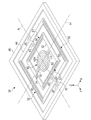
- FIG. It is a schematic perspective view which shows an example of a structure of a MEMS mirror.
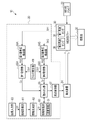
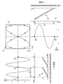
- It is a block diagram which shows an example of the functional structure of a control apparatus. It is a figure explaining an example of reference point detection processing and measurement processing.
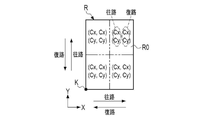
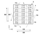
- FIG. 4 is a diagram showing an example of a plurality of partial regions obtained by dividing a scanning region; It is a figure which shows an example of a unit area.
- FIG. 4 is a diagram showing an example of a scanning area represented by a unit area;
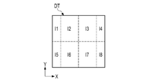
- FIG. 3 is a diagram showing an example of signal intensities forming image data; It is a figure which shows an example of intensity
- FIG. 10 is a diagram showing an example in which two or more lines forming a Lissajous curve cross each other in each partial area;
- FIG. 10 is a diagram showing an example in which four lines intersect a partial area;
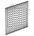
- It is a figure which shows the example which scanned the laser beam on the inclined projection surface.
- It is a block diagram showing an example of functional composition of a control device concerning a 2nd embodiment. It is a figure explaining the 1st example which changes a frequency ratio. It is a figure explaining the 2nd example which changes a phase difference.
- FIG. 11 is a diagram illustrating a third example of changing amplitude;
- FIG. 11 is a diagram illustrating a third embodiment in which the scanning period is longer than the frame period;
- FIG. 14 is a block diagram showing an example of a functional configuration of a control device according to a fourth embodiment;
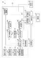
- FIG. 1 shows an example of the configuration of an image forming apparatus 10 of this embodiment.
- the image forming apparatus 10 of this embodiment includes a control device 20 , a MEMS (Micro Electro Mechanical Systems) driver 22 , a light emitting device 24 , a combining optical system 26 , a collimator 28 and a MEMS mirror 30 .
- the MEMS mirror 30 is an example of an “optical scanning device” according to the technology of the present disclosure.
- the light emitting device 24 has a laser driver 25 and a laser light source 27 .
- the laser driver 25 of this embodiment drives the laser light source 27 based on the intensity-modulated signal supplied from the control device 20 and causes the laser light source 27 to output laser light for forming an image.
- the laser light source 27 outputs three-color laser light, for example, R (Red), G (Green), and B (B: Blue).
- the laser light output from the laser light source 27 is combined by the combining optical system 26 and then irradiated onto the MEMS mirror 30 via the collimator 28 .
- the laser light focused on the MEMS mirror 30 is reflected by the MEMS mirror 30 toward the projection plane 32 .
- the projection plane 32 is, for example, a screen for projecting an image, or the retina of the human eye. That is, the image forming apparatus 10 of this embodiment is used for a projector, AR (Augmented Reality) glasses, or the like.
- the projection plane 32 in this embodiment is not limited to the surface of an actual object such as a screen, but also includes a virtual plane in space.
- the MEMS driver 22 drives the MEMS mirror 30 based on the control from the control device 20.
- the mirror portion 40 (see FIG. 2) that reflects the laser light independently swings about two axes orthogonal to each other.
- the projection plane 32 is scanned with laser light in a state of drawing a Lissajous curve by swinging the mirror section 40 based on the drive signal.
- a Lissajous curve is a curve determined by the oscillation frequency about the first axis, the oscillation frequency about the second axis, and the phase difference between them.
- the mirror unit 40 is an example of a “movable mirror” according to the technology of the present disclosure.
- the control device 20 of this embodiment includes an FPGA (Field Programmable Gate Array) 20A and a memory 20B.
- the memory 20B is, for example, a volatile memory, and stores various information such as an image signal representing an image to be projected onto the projection plane 32 .
- the memory 20B stores, for example, an image signal input from the outside of the image forming apparatus 10 .
- FIG. 2 shows an example of the configuration of the MEMS mirror 30.
- the MEMS mirror 30 has a mirror section 40 , a first support section 41 , a first movable frame 42 , a second support section 43 , a second movable frame 44 , a connection section 45 and a fixed frame 46 .
- the mirror section 40 has a reflecting surface 40A that reflects incident light.
- the reflecting surface 40A is formed of a metal thin film such as gold (Au), aluminum (Al), silver (Ag), or a silver alloy.
- the shape of the reflecting surface 40A is, for example, circular.
- the first support portions 41 are arranged outside the mirror portion 40 at positions opposed to each other with the second axis a2 interposed therebetween.
- the first supporting portion 41 is connected to the mirror portion 40 on the first axis a1, and supports the mirror portion 40 so as to be swingable about the first axis a1.
- the first movable frame 42 is a rectangular frame surrounding the mirror section 40, and is connected to the mirror section 40 via the first support section 41 on the first axis a1.
- Piezoelectric elements 50 are formed on the first movable frame 42 at positions opposed to each other with the first axis a1 interposed therebetween.
- a pair of first actuators 51 are configured by forming two piezoelectric elements 50 on the first movable frame 42 .
- the pair of first actuators 51 are arranged at positions facing each other with the first axis a1 interposed therebetween.
- the first actuator 51 causes the mirror section 40 to swing about the first axis a1 by applying rotational torque about the first axis a1 to the mirror section 40 .
- the second support portions 43 are arranged outside the first movable frame 42 at positions opposed to each other with the first axis a1 interposed therebetween.
- the second support portion 43 is connected to the first movable frame 42 on the second axis a2, and supports the first movable frame 42 and the mirror portion 40 so as to be swingable about the second axis a2.
- the second support portion 43 is a torsion bar extending along the second axis a2.
- the second movable frame 44 is a rectangular frame surrounding the first movable frame 42, and is connected to the first movable frame 42 via the second support portion 43 on the second axis a2.
- Piezoelectric elements 50 are formed on the second movable frame 44 at positions opposed to each other with the second axis a2 interposed therebetween.
- a pair of second actuators 52 are configured by forming two piezoelectric elements 50 on the second movable frame 44 .
- the pair of second actuators 52 are arranged at positions facing each other with the second axis a2 interposed therebetween.
- the second actuator 52 causes the mirror section 40 to swing about the second axis a2 by applying rotational torque about the second axis a2 to the mirror section 40 and the first movable frame 42 .
- the connecting portions 45 are arranged outside the second movable frame 44 at positions opposed to each other with the first axis a1 interposed therebetween.
- the connecting portion 45 is connected to the second movable frame 44 on the second axis a2.
- the fixed frame 46 is a rectangular frame that surrounds the second movable frame 44 and is connected to the second movable frame 44 via a connecting portion 45 on the second axis a2.
- a first angle sensor 34 is provided in the vicinity of the first support portion 41 on the first movable frame 42 .
- the first angle sensor 34 is composed of a piezoelectric element, and converts the force applied by the deformation of the first support portion 41 as the mirror portion 40 oscillates about the first axis a1 into a voltage to generate a signal. to output That is, the first angle sensor 34 outputs a signal (hereinafter referred to as a first angle signal) SA1 representing the deflection angle of the mirror section 40 about the first axis a1.
- the first angle signal SA1 is a sine wave having an oscillation frequency of the mirror section 40 around the first axis a1.
- a second angle sensor 36 is provided in the vicinity of the second support portion 43 on the second movable frame 44 .
- the second angle sensor 36 is composed of a piezoelectric element, and converts the force applied by the deformation of the second support portion 43 as the mirror portion 40 oscillates around the second axis a2 into a voltage to generate a signal. to output That is, the second angle sensor 36 outputs a signal (hereinafter referred to as a second angle signal) SA2 representing the deflection angle of the mirror section 40 about the second axis a2.
- the second angle signal SA2 is a sine wave having an oscillation frequency of the mirror section 40 around the second axis a2.
- first axis a1 and the second axis a2 are orthogonal to each other.
- the direction parallel to the first axis a1 is the X direction
- the direction parallel to the second axis a2 is the Y direction
- the direction orthogonal to the first axis a1 and the second axis a2 is the Z direction. direction.
- FIG. 3 shows an example of the functional configuration of the control device 20.
- the control device 20 includes an image input unit 60, an image storage unit 61, an information generation unit 62, an information storage unit 63, a first reference point detection unit 64A, a second reference point detection unit 64B, a A first measuring section 65A, a second measuring section 65B, a reading section 66, and a light emission control section 67 are configured. These functional units are realized by cooperative operation of the FPGA 20A and the memory 20B.
- Image data DT representing an image to be formed is input to the image input unit 60 from the outside.
- an image corresponding to the image data DT input to the image input unit 60 may be referred to as an input image.
- color image data DT represented by RGB signals is input to the image input unit 60 .
- Image data DT input to the image input unit 60 is output to the image storage unit 61 .
- the image storage section 61 is a memory that stores the image data DT output from the image input section 60 .
- the image data DT input to the image input unit 60 is not limited to this embodiment, and may be data corresponding to an image to be formed. For example, it may be binarized data representing whether or not to output a laser beam. Alternatively, for example, it may be data representing multiple values of the output amount.
- the information generation unit 62 generates intensity information SI representing the correspondence relationship between a first count value Cx and a second count value Cy, which will be described later, and the signal intensity of the input image. If the input image is a color image, the signal strength represents the strength of each of the RGB signals.
- the information storage section 63 is a memory that stores the intensity information SI generated by the information generation section 62 . Note that the first count value Cx is an example of the "first elapsed time" according to the present embodiment. The second count value Cy is an example of the "second elapsed time” according to this embodiment.
- the first reference point detector 64A detects the first reference point P1 based on the first angle signal SA1 output from the first angle sensor 34, as shown in FIG.
- the first reference point P1 is the time at which the deflection angle of the mirror section 40 about the first axis a1 reaches the first reference angle ⁇ 1.
- the first reference angle ⁇ 1 is 0°.
- the first reference angle ⁇ 1 is not limited to 0°, and may be an angle at which the deflection angle is the maximum value or the minimum value.
- First reference point detection unit 64A generates pulse signal PS1 in response to detection of first reference point P1.
- the first reference point detection section 64A sets the time at which the deflection angle of the mirror section 40 about the first axis a1 changes from negative to positive to 0° as the first reference point P1. To detect.
- the first reference point detection section 64A outputs the pulse signal PS1 to the first measurement section 65A.
- the second reference point detection section 64B detects the second reference point P2 based on the second angle signal SA2 output from the second angle sensor 36, as shown in FIG.
- the second reference point P2 is the time at which the deflection angle of the mirror section 40 about the second axis a2 reaches the second reference angle ⁇ 2.
- the second reference angle ⁇ 2 is 0°. It should be noted that the second reference angle ⁇ 2 is not limited to 0°, and may be an angle at which the deflection angle becomes the maximum value or the minimum value.
- the second reference point detector 64B generates a pulse signal PS2 in response to detecting the second reference point P2.
- the second reference point detection section 64B sets the time at which the deflection angle of the mirror section 40 about the second axis a2 changes from negative to positive and becomes 0° as the second reference point P2. To detect.
- the second reference point detection section 64B outputs the pulse signal PS2 to the second measurement section 65B.
- the first measurement unit 65A performs a first measurement process of measuring the elapsed time from the first reference point P1 detected by the first reference point detection unit 64A as a first count value Cx.
- the second measurement section 65B performs a second measurement process of measuring the elapsed time from the second reference point P2 detected by the second reference point detection section 64B as a second count value Cy.
- a clock signal CLK is supplied from the clock generator 68 to the first measuring section 65A and the second measuring section 65B.
- the clock generator 68 generates an oscillation period T1 about the first axis a1 of the mirror section 40 (hereinafter referred to as the first oscillation period T1) and an oscillation period T2 about the second axis a2 (hereinafter referred to as the second oscillation period T1).
- a clock signal CLK having a sufficiently shorter clock period than the oscillation period T2 is generated.
- the clock signal CLK is a system clock signal supplied to each section within the control device 20 .
- the first measurement section 65A uses the count value obtained by counting up the clock signal CLK from the first reference point P1 as the first count value Cx.
- the first measurement unit 65A resets the count value to zero every first oscillation period T1 in synchronization with the pulse signal PS1.
- the second measurement section 65B uses the count value obtained by counting up the clock signal CLK from the second reference point P2 based on the pulse signal PS2 output from the second reference point detection section 64B as the second count value Cy.
- the second measurement section 65B resets the count value to zero every second oscillation period T2 in synchronization with the pulse signal PS2.
- the first count value Cx measured by the first measurement unit 65A and the second count value Cy measured by the second measurement unit 65B are supplied to the reading unit 66, respectively.
- the reading unit 66 obtains signal intensities corresponding to the first count value Cx and the second count value Cy supplied from the first measuring unit 65A and the second measuring unit 65B from the intensity information SI stored in the information storage unit 63. Perform read processing to read.
- the reading unit 66 supplies the signal intensity read from the intensity information SI to the light emission control unit 67 .
- the light emission control unit 67 performs light emission control processing for causing the light emitting device 24 to perform intensity modulation of the laser light based on the signal intensity supplied from the reading unit 66 . Specifically, intensity modulation is performed by the laser driver 25 described above.
- the laser light source 27 outputs a laser beam having an intensity corresponding to the signal intensity supplied from the reading section 66 .
- the intensity of the laser light is modulated for each color of RGB.
- the first reference point detection section 64A, the second reference point detection section 64B, the first measurement section 65A, the second measurement section 65B, the reading section 66, and the light emission control section 67 operate at each clock cycle of the clock signal CLK. . That is, the laser light is intensity-modulated for each clock cycle according to the first count value Cx and the second count value Cy.
- the MEMS driver 22 is arranged so that the ratio between the first oscillation period T1 and the second oscillation period T2 is 1:2 (that is, the frequency ratio is 2:1). , drives the MEMS mirror 30 . That is, the frequency ratio of the drive signals given to the first actuator 51 and the second actuator 52 is set to 2:1.
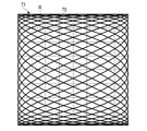
- the laser light emitted from the light emitting device 24 is scanned by the MEMS mirror 30 on the projection plane 32 so as to draw a figure-of-eight Lissajous curve 70 centered on the origin K. That is, the Lissajous curve 70 represents the scanning path of the Lissajous scanning.
- the frequency ratio of the driving signals is set to 2:1 for simplification of explanation.
- the frequency ratio and phase difference of the driving signals are preferably determined so that the scanning cycle TL of the Lissajous scanning is lengthened and the Lissajous curve 70 is made denser.
- the information generator 62 generates intensity information SI based on the correspondence relationship between the path of the Lissajous curve 70 represented by the first count value Cx and the second count value Cy and the signal intensity of the input image.
- a rectangular scanning area 71 including a Lissajous curve 70 is divided into eight. Specifically, it is divided into four in the X direction and divided into two in the Y direction.
- Each of the partial regions R obtained by dividing the scanning region 71 corresponds to a scanning length of two clock cycles in the X direction and the Y direction.
- one line forming the Lissajous curve 70 intersects each of the partial regions R.
- an image is formed by emitting intensity-modulated laser light once in each partial region R. That is, the partial regions R correspond to pixels (drawing units) of the image formed on the projection plane 32 .
- FIG. 6 is a diagram in which the partial region R is divided into a plurality of unit regions R0 in units of clock cycles.
- the scanning position reciprocates in the X and Y directions, so there are four passing directions of the scanning position passing through the unit area R0, ie, forward and backward directions in each of the X and Y directions.
- the outward path refers to a movement path in a direction away from the origin K
- the return path refers to a movement path in a direction to approach the origin K.
- the Cx on the left represents the first count value Cx on the forward pass
- the Cx on the right represents the first count value Cx on the return pass.
- the left Cy represents the second count value Cy for the forward trip
- the right Cy represents the second count value Cy for the return trip.
- FIG. 7 is a diagram showing each partial area R that configures the scanning area 71 by a plurality of unit areas R0.
- Each partial region R is represented using a first count value Cx and a second count value Cy.
- the upper bracket represents (Cx, Cx) and the lower bracket represents (Cy, Cy).
- FIG. 8 shows an example of the signal intensity I forming the image data DT.
- the information generator 62 divides the image data DT as an input image so as to correspond to the partial regions R forming the scanning region 71 .
- the information generator 62 obtains the signal intensity I for each divided area obtained by dividing the image data DT.
- the signal intensity I is obtained by averaging a plurality of pixel signals included in the divided area for each color of RGB.
- Signal intensity I represents the intensity of each of the RGB signals.
- eight signal intensities I1 to I8 are obtained from the image data DT.
- FIG. 9 shows an example of intensity information SI.
- the information generator 62 generates intensity information SI by associating the signal intensity I with the first count value Cx and the second count value Cy.
- the information generation unit 62 associates the signal intensities I1 to I8 obtained from the image data DT with the first count value Cx and the second count value Cy of the corresponding partial regions R, respectively, thereby generating the intensity information SI. to generate
- the intensity information SI is represented as a matrix table with the first count value Cx and the second count value Cy as parameters, and the signal intensity I corresponding to all combinations of the first count value Cx and the second count value Cy. holding Therefore, even if the relationship between the first reference point P1 and the second reference point P2 changes and the phase difference between the first angle signal SA1 and the second angle signal SA2 changes, the intensity information SI is can be used in common.
- the information generator 62 should change the signal strength I in the strength information SI for each frame according to the image represented by each frame. Just do it.
- the frame period TF and the scanning period TL are set to be the same.
- FIG. 10 shows an example of readout processing by the readout unit 66.
- the reading unit 66 receives the first count value Cx and the second count value Cy from the first measuring unit 65A and the second measuring unit 65B for each clock cycle of the clock signal CLK.
- the light emission control unit 67 causes the light emitting device 24 to perform intensity modulation of the laser light based on the signal intensity I6 read by the readout unit 66 .
- the control device 20 sets the elapsed time from the first reference point P1 at which the deflection angle of the mirror portion 40 about the first axis a1 becomes the first reference angle ⁇ 1 to the first count value Cx (the first count value Cx). 1 elapsed time), and the elapsed time from the second reference point P2 at which the deflection angle of the mirror portion 40 about the second axis a2 becomes the second reference angle ⁇ 2 is the second count value Cy (second elapsed time ). Then, the control device 20 acquires the signal intensity I corresponding to the measured first count value Cx and second count value Cy from the intensity information SI, and causes the light emitting device 24 to perform intensity modulation of the laser beam.
- the control device 20 does not need to generate an origin signal that defines the scanning cycle TL of Lissajous scanning, unlike the conventional art.
- the scanning period TL may vary due to the rotational moment of the mirror unit 40, gravity, air pressure, etc.
- the first elapsed time and the second elapsed time are calculated without using the origin signal. Since the light emission timing is controlled based on time, even if the scan period fluctuates, it is possible to suppress the deviation between the scan period TL and the light emission timing.
- control device 20 independently measures the first elapsed time and the second elapsed time. Therefore, according to the technique of the present disclosure, it is possible to perform robust image formation that is not affected by fluctuations in the phase difference between the oscillation of the mirror section 40 about the first axis a1 and the oscillation about the second axis a2. can be done. Further, according to the technique of the present disclosure, since it is not necessary to correct the drive signal so that the phase difference is kept constant, even during Lissajous scanning, the oscillation frequency around the two axes, the frequency ratio, It is possible to dynamically change the phase difference, or the amplitude. As a result, the resolution, frame rate, angle of view, amount of light, etc. of the image formed on the projection plane 32 can be dynamically switched.
- the MEMS driver 22 drives the MEMS mirror 30 so that the scanning position of the laser light draws a figure-of-eight Lissajous curve 70.
- the MEMS mirror 30 may be driven so as to draw a dense Lissajous curve 70 .
- the resolution of the image formed on the projection plane 32 can be increased.
- the scanning region 71 is divided so that one line forming the Lissajous curve 70 intersects with each of the partial regions R.
- the scanning area 71 may be divided so that two or more cross each other. In the example shown in FIG. 11, two or more lines forming the Lissajous curve 70 cross each of the partial regions R. In the example shown in FIG.
- FIG. 12 shows an example in which four lines 70A to 70D intersect the partial area R.
- FIG. Four lines 70A to 70D shown in FIG. 11 constitute one Lissajous curve 70 as a whole.
- the intensity modulation of the laser light is performed with the same signal intensity I when the scanning position passes through the partial area R shown in FIG. 12 along each of the four lines 70A to 70D.
- Intensity modulation of the laser light is performed with the same signal intensity I in the range.
- the laser beam is scanned perpendicularly to the planar projection surface 32, but it is also conceivable that the projection surface 32 is inclined.
- the Lissajous curve 70 drawn by the laser beam scanned on the projection plane 32 is deformed as shown in FIG. 13 as an example.
- the information generator 62 may generate the intensity information SI based on the deformed Lissajous curve 70 .
- FIG. 14 shows an example of the functional configuration of the control device 20 according to the second embodiment.
- the functional configuration of the control device 20 according to the second embodiment has a scanning path changing unit 80 in addition to the functional configuration of the control device 20 according to the first embodiment.
- the scanning path changing unit 80 changes the scanning path of Lissajous scanning by laser light by controlling the drive signal for driving the MEMS mirror 30 by the MEMS driver 22 . That is, the scanning path changing unit 80 changes the shape or size of the Lissajous curve 70 .
- the scanning path changing unit 80 changes the scanning path, for example, every frame period TF.
- the scanning path is switched every one frame period TF, and the current scanning path passes through the area that the previous scanning path did not pass, so that scanning in the scanning area 71 can be made dense. As a result, the resolution of the image formed on the projection plane 32 is further improved.
- the information storage unit 63 stores intensity information SI corresponding to each of two or more scanning paths changed by the scanning path changing unit 80 .
- the reading unit 66 reads the signal intensity I from the intensity information SI corresponding to the scanning path changed by the scanning path changing unit 80 .
- the scanning path changing section 80 changes the frequency of at least one of the oscillation of the mirror section 40 around the first axis a1 and the oscillation around the second axis a2 (that is, changes the frequency ratio to change) to change the scanning path of Lissajous scanning.
- the scanning path changer 80 changes the frequency ratio between 2:1 and 3:1.
- changing the frequency ratio changes the scanning period TL of Lissajous scanning, so it is also preferable to change the frequency ratio so that the scanning period TL does not change.
- the frequency ratio between 3:1 and 1:3, the scanning path can be changed while maintaining the scanning period TL constant.
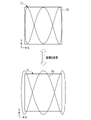
- the scanning path changing unit 80 changes the phase difference between the swinging of the mirror unit 40 about the first axis a1 and the swinging about the second axis a2 so as to perform Lissajous scanning. Change route. As an example, as shown in FIG. 16, the phase difference ⁇ is switched between 90° and 180° while keeping the frequency ratio at 3:1. By changing the Lissajous curve 70 in this way, the scanning in the scanning area 71 becomes denser.
- the scanning path changing unit 80 changes the amplitude of at least one of the oscillation of the mirror unit 40 about the first axis a1 and the oscillation about the second axis a2, thereby adjusting the Lissajous motion. Change the scan path of the scan. As an example, as shown in FIG. 17, increasing the amplitude increases the scanning range (that is, the Lissajous curve 70 increases). By changing the Lissajous curve 70 in this way, the scanning in the scanning area 71 becomes denser.
- the scanning range is expanded when the amplitude is increased, the amount of light per pixel of the image formed on the projection plane 32 is relatively decreased compared to before the amplitude is increased. Therefore, it is preferable to increase the intensity of the laser beam so as to compensate for the reduction in the amount of light due to the increased amplitude.
- the scanning path changing unit 80 changes the scanning path between two types of scanning paths. may be changed. Further, the scanning path changing section 80 may change the scanning path of Lissajous scanning by a combination of two or more of frequency, phase difference, and amplitude.
- the scanning period TL is matched with the frame period TF, but in the third embodiment, the scanning period TL is made longer than the frame period TF (that is, TL>TF).
- the first reference point detection section 64A and the second reference point detection section 64B detect the first reference point P1 and the second reference point P1 based on the first angle signal SA1 and the second angle signal SA2, respectively. Although the two reference points P2 are generated, the first angle signal SA1 and the second angle signal SA2 need not be generated by the first angle sensor 34 and the second angle sensor 36, respectively.
- the controller 20 is provided with an angle signal generator 90 that generates the first angle signal SA1 and the second angle signal SA2.
- the angle signal generation unit 90 performs calculations for estimating the deflection angle of the mirror unit 40 about the first axis a1 and the deflection angle about the second axis a2 based on the drive signal by which the MEMS driver 22 drives the MEMS mirror 30. By performing processing, a first angle signal SA1 and a second angle signal SA2 are generated.
- the angle signal generator 90 supplies the generated first angle signal SA1 and second angle signal SA2 to the first reference point detector 64A and the second reference point detector 64B, respectively.
- the angle signal generator 90 may generate the first angle signal SA1 and the second angle signal SA2 using a learned model learned by machine learning. Note that in the present embodiment, the MEMS mirror 30 may not be provided with the first angle sensor 34 and the second angle sensor 36 .
- the following various processors can be used.
- the CPU Central Processing Unit
- the above-mentioned various processors include the above-mentioned FPGA, etc., whose circuit configuration can be changed after manufacturing.
- Programmable Logic Device which is a processor, ASIC (Application Specific Integrated Circuit), etc. be
- One processing unit may be configured with one of these various processors, or a combination of two or more processors of the same or different type (for example, a combination of a plurality of FPGAs and/or a CPU and combination with FPGA). Also, a plurality of processing units may be configured by one processor.
- the image input unit 60 may be an image input processor.
- the image storage unit 61 may be an image storage memory.
- the information generator 62 may be an information generation processor.
- the information storage unit 63 may be an information storage memory.
- the first reference point detector 64A may be a first reference point detection processor.
- the second reference point detection unit 64B may be a second reference point detection processor.
- the first measurement unit 65A may be a first measurement processor.
- the second measurement unit 65B may be a second measurement processor.
- the readout unit 66 may be a readout processor.
- the light emission controller 67 may be a light emission control processor.
- the angle signal generator 90 may be an angle signal generation processor.
- a single processor is configured by combining one or more CPUs and software.
- a processor functions as multiple processing units.
- SoC System On Chip
- a processor that realizes the functions of the entire system including multiple processing units with a single IC (Integrated Circuit) chip. be.
- the various processing units are configured using one or more of the above various processors as a hardware structure.
Landscapes
- Physics & Mathematics (AREA)
- General Physics & Mathematics (AREA)
- Optics & Photonics (AREA)
- Engineering & Computer Science (AREA)
- Computer Hardware Design (AREA)
- Theoretical Computer Science (AREA)
- Mechanical Optical Scanning Systems (AREA)
Abstract
Description
図1には、本実施形態の画像形成装置10の構成の一例を示す。図1に示すように本実施形態の画像形成装置10は、制御装置20、MEMS(Micro Electro Mechanical Systems)ドライバ22、発光装置24、合波光学系26、コリメータ28、及びMEMSミラー30を備える。MEMSミラー30は、本開示の技術に係る「光走査装置」の一例である。
次に、第2実施形態について説明する。図14は、第2実施形態に係る制御装置20の機能構成の一例を示す。第2実施形態に係る制御装置20の機能構成は、第1実施形態に係る制御装置20の機能構成に加えて、走査経路変更部80を有する。走査経路変更部80は、MEMSドライバ22がMEMSミラー30を駆動するための駆動信号を制御することにより、レーザ光によるリサージュ走査の走査経路を変更する。すなわち、走査経路変更部80は、リサージュ曲線70の形状又は大きさを変更する。
次に、第3実施形態について説明する。第1実施形態では、走査周期TLをフレーム周期TFに一致させているが、第3実施形態では、走査周期TLをフレーム周期TFよりも長くする(すなわちTL>TFとする)。一例として図18に示すように、走査周期TLをフレーム周期TFの二倍とする(すなわちTL=2×TFとする)。
次に、第4実施形態について説明する。第1実施形態に係る制御装置20では、第1基準点検出部64A及び第2基準点検出部64Bは、それぞれ第1角度信号SA1及び第2角度信号SA2に基づいて第1基準点P1及び第2基準点P2を生成しているが、第1角度信号SA1及び第2角度信号SA2は、第1角度センサ34及び第2角度センサ36により生成されたものでなくてもよい。第4実施形態では、図19に示すように、制御装置20内に、第1角度信号SA1及び第2角度信号SA2を生成する角度信号生成部90を設ける。
Claims (12)
- 第1軸及び第2軸の周りに揺動する可動ミラーに、入力画像に応じて強度を変調した光を照射することにより光をリサージュ走査する光走査装置を制御する制御装置であって、
前記可動ミラーの前記第1軸周りの振れ角が第1基準角となった第1基準点からの経過時間を、第1経過時間として計測する第1計測部と、
前記可動ミラーの前記第2軸周りの振れ角が第2基準角となった第2基準点からの経過時間を、第2経過時間として計測する第2計測部と、
前記第1経過時間及び前記第2経過時間と、前記入力画像の信号強度との対応関係を表す強度情報を記憶した情報記憶部と、
前記第1計測部により計測された前記第1経過時間と、前記第2計測部により計測された前記第2経過時間とに対応する前記信号強度を前記情報記憶部から読み出す読み出し部と、
前記読み出し部により読み出された前記信号強度に基づいて、発光装置に前記光の強度変調を行わせる発光制御部と、
を備える制御装置。 - 前記第1計測部及び前記第2計測部は、クロック発生器から出力されるクロック信号をカウントすることにより、前記第1経過時間及び前記第2経過時間をそれぞれ計測する、
請求項1に記載の制御装置。 - 前記第1基準点を検出する第1基準点検出部と、前記第2基準点を検出する第2基準点検出部とを備える、
請求項1又は請求項2に記載の制御装置。 - 前記光走査装置は、前記可動ミラーの前記第1軸周りの振れ角に応じた第1角度信号を出力する第1角度センサと、前記可動ミラーの前記第2軸周りの振れ角に応じた第2角度信号を出力する第2角度センサとを有し、
前記第1基準点検出部は、前記第1角度センサから出力される前記第1角度信号に基づいて前記第1基準点を検出し、
前記第2基準点検出部は、前記第2角度センサから出力される前記第2角度信号に基づいて前記第2基準点を検出する、
請求項3に記載の制御装置。 - 前記強度情報は、前記第1経過時間と前記第2経過時間との組み合わせと、前記入力画像の信号強度との対応関係を表す、
請求項1から請求項4のうちいずれか1項に記載の制御装置。 - 前記可動ミラーの前記第1軸周りの揺動と前記第2軸周りの揺動とのうち少なくとも一方の周波数を変更することにより、リサージュ走査の走査経路を変更する走査経路変更部を有する、
請求項3に記載の制御装置。 - 前記可動ミラーの前記第1軸周りの揺動と前記第2軸周りの揺動との位相差を変更することにより、リサージュ走査の走査経路を変更する走査経路変更部を備える、
請求項3に記載の制御装置。 - 前記可動ミラーの前記第1軸周りの揺動と前記第2軸周りの揺動とのうち少なくとも一方の振幅を変更することにより、リサージュ走査の走査経路を変更する走査経路変更部を備える、
請求項3に記載の制御装置。 - 前記可動ミラーの前記第1軸周りの揺動と前記第2軸周りの揺動とのうち少なくともいずれか一方の周波数を変更すること、
前記可動ミラーの前記第1軸周りの揺動と前記第2軸周りの揺動との位相差を変更すること、
前記可動ミラーの前記第1軸周りの揺動と前記第2軸周りの揺動とのうち少なくともいずれか一方の振幅を変更すること、
のうちの少なくとも2つの組み合わせにより、リサージュ走査の走査経路を変更する走査経路変更部を備える、
請求項3に記載の制御装置。 - リサージュ走査の走査周期は、前記入力画像のフレーム周期よりも長い、
請求項1から請求項9のうちいずれか1項に記載の制御装置。 - 請求項1から請求項10のうちいずれか1項に記載の制御装置と、
前記光走査装置と、
前記発光装置と、
を備える画像形成装置。 - 第1軸及び第2軸の周りに揺動する可動ミラーに、入力画像に応じて強度を変調した光を照射することにより光をリサージュ走査する光走査装置を制御する制御方法であって、
前記可動ミラーの前記第1軸周りの振れ角が第1基準角となった第1基準点からの経過時間を、第1経過時間として計測する第1計測処理と、
前記可動ミラーの前記第2軸周りの振れ角が第2基準角となった第2基準点からの経過時間を、第2経過時間として計測する第2計測処理と、
前記第1経過時間及び前記第2経過時間と、前記入力画像の信号強度との対応関係を表す強度情報を記憶した情報記憶部から、前記第1計測処理により計測された前記第1経過時間と、前記第2計測処理により計測された前記第2経過時間とに対応する前記信号強度を読み出す読み出し処理と、
前記読み出し処理により読み出された前記信号強度に基づいて、発光装置に前記光の強度変調を行わせる発光制御処理と、
を実行する制御方法。
Priority Applications (4)
| Application Number | Priority Date | Filing Date | Title |
|---|---|---|---|
| JP2023508656A JP7707281B2 (ja) | 2021-03-25 | 2022-01-12 | 制御装置、画像形成装置、及び制御方法 |
| CN202280020477.9A CN117015733A (zh) | 2021-03-25 | 2022-01-12 | 控制装置、图像形成装置及控制方法 |
| EP22774559.3A EP4318074B1 (en) | 2021-03-25 | 2022-01-12 | Control device, image forming device, and control method |
| US18/469,646 US20240004186A1 (en) | 2021-03-25 | 2023-09-19 | Control device, image forming apparatus, and control method |
Applications Claiming Priority (2)
| Application Number | Priority Date | Filing Date | Title |
|---|---|---|---|
| JP2021051663 | 2021-03-25 | ||
| JP2021-051663 | 2021-03-25 |
Related Child Applications (1)
| Application Number | Title | Priority Date | Filing Date |
|---|---|---|---|
| US18/469,646 Continuation US20240004186A1 (en) | 2021-03-25 | 2023-09-19 | Control device, image forming apparatus, and control method |
Publications (1)
| Publication Number | Publication Date |
|---|---|
| WO2022201754A1 true WO2022201754A1 (ja) | 2022-09-29 |
Family
ID=83396839
Family Applications (1)
| Application Number | Title | Priority Date | Filing Date |
|---|---|---|---|
| PCT/JP2022/000785 Ceased WO2022201754A1 (ja) | 2021-03-25 | 2022-01-12 | 制御装置、画像形成装置、及び制御方法 |
Country Status (5)
| Country | Link |
|---|---|
| US (1) | US20240004186A1 (ja) |
| EP (1) | EP4318074B1 (ja) |
| JP (1) | JP7707281B2 (ja) |
| CN (1) | CN117015733A (ja) |
| WO (1) | WO2022201754A1 (ja) |
Cited By (1)
| Publication number | Priority date | Publication date | Assignee | Title |
|---|---|---|---|---|
| WO2025057631A1 (ja) * | 2023-09-14 | 2025-03-20 | 富士フイルム株式会社 | 光走査装置、画像描画システム、及び光走査装置の駆動方法 |
Families Citing this family (1)
| Publication number | Priority date | Publication date | Assignee | Title |
|---|---|---|---|---|
| JP7481099B2 (ja) * | 2019-09-11 | 2024-05-10 | 浜松ホトニクス株式会社 | 光走査システムの製造方法、光走査装置の製造方法及びデータ取得方法 |
Citations (4)
| Publication number | Priority date | Publication date | Assignee | Title |
|---|---|---|---|---|
| JP2012247534A (ja) * | 2011-05-26 | 2012-12-13 | Ricoh Co Ltd | 電磁波の走査方法、映像投影装置および画像取得装置 |
| JP2016014749A (ja) | 2014-07-01 | 2016-01-28 | 日本信号株式会社 | 光走査装置 |
| CN109752839A (zh) * | 2018-12-18 | 2019-05-14 | 华为技术有限公司 | 处理器、显示控制装置、系统、图像处理方法及装置 |
| CN111722238A (zh) * | 2019-03-19 | 2020-09-29 | 中国科学院苏州纳米技术与纳米仿生研究所 | 基于双轴谐振式mems微镜的扫描控制系统及控制方法 |
Family Cites Families (4)
| Publication number | Priority date | Publication date | Assignee | Title |
|---|---|---|---|---|
| WO2006082827A1 (ja) * | 2005-02-02 | 2006-08-10 | Brother Kogyo Kabushiki Kaisha | 光走査型ディスプレイおよびそれの駆動方法 |
| DE102008043416A1 (de) * | 2008-11-03 | 2010-05-06 | Robert Bosch Gmbh | Mikromechanisches Bauteil und Verfahren zum Betreiben eines mikromechanischen Bauteils |
| JP5587403B2 (ja) * | 2010-04-28 | 2014-09-10 | パナソニック株式会社 | 走査型画像表示装置 |
| US10939080B2 (en) * | 2019-03-29 | 2021-03-02 | Facebook Technologies, Llc | Trajectory estimation for a MEMS reflector |
-
2022
- 2022-01-12 JP JP2023508656A patent/JP7707281B2/ja active Active
- 2022-01-12 CN CN202280020477.9A patent/CN117015733A/zh active Pending
- 2022-01-12 WO PCT/JP2022/000785 patent/WO2022201754A1/ja not_active Ceased
- 2022-01-12 EP EP22774559.3A patent/EP4318074B1/en active Active
-
2023
- 2023-09-19 US US18/469,646 patent/US20240004186A1/en active Pending
Patent Citations (4)
| Publication number | Priority date | Publication date | Assignee | Title |
|---|---|---|---|---|
| JP2012247534A (ja) * | 2011-05-26 | 2012-12-13 | Ricoh Co Ltd | 電磁波の走査方法、映像投影装置および画像取得装置 |
| JP2016014749A (ja) | 2014-07-01 | 2016-01-28 | 日本信号株式会社 | 光走査装置 |
| CN109752839A (zh) * | 2018-12-18 | 2019-05-14 | 华为技术有限公司 | 处理器、显示控制装置、系统、图像处理方法及装置 |
| CN111722238A (zh) * | 2019-03-19 | 2020-09-29 | 中国科学院苏州纳米技术与纳米仿生研究所 | 基于双轴谐振式mems微镜的扫描控制系统及控制方法 |
Non-Patent Citations (1)
| Title |
|---|
| See also references of EP4318074A4 |
Cited By (1)
| Publication number | Priority date | Publication date | Assignee | Title |
|---|---|---|---|---|
| WO2025057631A1 (ja) * | 2023-09-14 | 2025-03-20 | 富士フイルム株式会社 | 光走査装置、画像描画システム、及び光走査装置の駆動方法 |
Also Published As
| Publication number | Publication date |
|---|---|
| US20240004186A1 (en) | 2024-01-04 |
| EP4318074A1 (en) | 2024-02-07 |
| JPWO2022201754A1 (ja) | 2022-09-29 |
| EP4318074A4 (en) | 2024-10-02 |
| EP4318074B1 (en) | 2025-04-09 |
| JP7707281B2 (ja) | 2025-07-14 |
| CN117015733A (zh) | 2023-11-07 |
Similar Documents
| Publication | Publication Date | Title |
|---|---|---|
| US8395633B2 (en) | Scanning type image display apparatus | |
| CN109752839B (zh) | 处理器、显示控制装置、系统、图像处理方法及装置 | |
| JP2019082634A (ja) | 可動装置、ヘッドアップディスプレイ、レーザヘッドランプ、ヘッドマウントディスプレイ、車両及び光走査方法 | |
| US12320971B2 (en) | Optical scanning device, driving method of optical scanning device, and image drawing system | |
| US20240004186A1 (en) | Control device, image forming apparatus, and control method | |
| JP4840175B2 (ja) | 画像表示装置 | |
| US12339438B2 (en) | Micromirror device and optical scanning device | |
| JP5494225B2 (ja) | 画像形成装置 | |
| JP7172557B2 (ja) | 光偏向装置、画像投影装置、レーザヘッドランプ及び移動体 | |
| JP2017227868A (ja) | 制御装置、画像投影装置、および制御方法 | |
| JP2018010276A (ja) | 圧電アクチュエータ、光偏向器及び画像投影装置 | |
| CN117647888A (zh) | 图片生成单元中的多束激光束扫描仪 | |
| JP5565270B2 (ja) | 走査方法、映像投影装置および画像取得装置 | |
| JP5842388B2 (ja) | 電磁波の走査方法、映像投影装置および画像取得装置 | |
| US12302041B2 (en) | Optical scanning device, driving method of optical scanning device, and image drawing system | |
| JP2021081593A (ja) | 台座、可動装置、レーザレーダ装置、画像形成装置及び画像投影装置 | |
| US20250350699A1 (en) | Image drawing apparatus and driving method for image drawing apparatus | |
| JP7396147B2 (ja) | 可動装置、光偏向装置、画像投影装置、光書込装置、物体認識装置、移動体、ヘッドマウントディスプレイ | |
| US20260009999A1 (en) | Optical scanning device, image drawing system, and driving method of mirror device | |
| WO2025057631A1 (ja) | 光走査装置、画像描画システム、及び光走査装置の駆動方法 | |
| JP3342712B2 (ja) | 立体動画像表示方法および装置 | |
| WO2025074825A1 (ja) | 光走査装置、及び光走査装置の駆動方法 | |
| JP7640373B2 (ja) | 画像形成装置、及びその作動方法 | |
| US20260079338A1 (en) | Mirror device and optical scanning device | |
| JP2012145754A (ja) | 画像表示装置 |
Legal Events
| Date | Code | Title | Description |
|---|---|---|---|
| 121 | Ep: the epo has been informed by wipo that ep was designated in this application |
Ref document number: 22774559 Country of ref document: EP Kind code of ref document: A1 |
|
| WWE | Wipo information: entry into national phase |
Ref document number: 2023508656 Country of ref document: JP |
|
| WWE | Wipo information: entry into national phase |
Ref document number: 202280020477.9 Country of ref document: CN |
|
| WWE | Wipo information: entry into national phase |
Ref document number: 2022774559 Country of ref document: EP |
|
| NENP | Non-entry into the national phase |
Ref country code: DE |
|
| ENP | Entry into the national phase |
Ref document number: 2022774559 Country of ref document: EP Effective date: 20231025 |
|
| WWG | Wipo information: grant in national office |
Ref document number: 2022774559 Country of ref document: EP |