WO2022202153A1 - 接着剤組成物、積層体、積層体の製造方法、及び半導体基板の製造方法 - Google Patents
接着剤組成物、積層体、積層体の製造方法、及び半導体基板の製造方法 Download PDFInfo
- Publication number
- WO2022202153A1 WO2022202153A1 PCT/JP2022/008678 JP2022008678W WO2022202153A1 WO 2022202153 A1 WO2022202153 A1 WO 2022202153A1 JP 2022008678 W JP2022008678 W JP 2022008678W WO 2022202153 A1 WO2022202153 A1 WO 2022202153A1
- Authority
- WO
- WIPO (PCT)
- Prior art keywords
- units
- group
- polyorganosiloxane
- adhesive
- adhesive composition
- Prior art date
- Legal status (The legal status is an assumption and is not a legal conclusion. Google has not performed a legal analysis and makes no representation as to the accuracy of the status listed.)
- Ceased
Links
Images



Classifications
-
- C—CHEMISTRY; METALLURGY
- C09—DYES; PAINTS; POLISHES; NATURAL RESINS; ADHESIVES; COMPOSITIONS NOT OTHERWISE PROVIDED FOR; APPLICATIONS OF MATERIALS NOT OTHERWISE PROVIDED FOR
- C09J—ADHESIVES; NON-MECHANICAL ASPECTS OF ADHESIVE PROCESSES IN GENERAL; ADHESIVE PROCESSES NOT PROVIDED FOR ELSEWHERE; USE OF MATERIALS AS ADHESIVES
- C09J183/00—Adhesives based on macromolecular compounds obtained by reactions forming in the main chain of the macromolecule a linkage containing silicon, with or without sulfur, nitrogen, oxygen, or carbon only; Adhesives based on derivatives of such polymers
- C09J183/04—Polysiloxanes
-
- H—ELECTRICITY
- H10—SEMICONDUCTOR DEVICES; ELECTRIC SOLID-STATE DEVICES NOT OTHERWISE PROVIDED FOR
- H10P—GENERIC PROCESSES OR APPARATUS FOR THE MANUFACTURE OR TREATMENT OF DEVICES COVERED BY CLASS H10
- H10P72/00—Handling or holding of wafers, substrates or devices during manufacture or treatment thereof
- H10P72/70—Handling or holding of wafers, substrates or devices during manufacture or treatment thereof for supporting or gripping
- H10P72/74—Handling or holding of wafers, substrates or devices during manufacture or treatment thereof for supporting or gripping using temporarily an auxiliary support
-
- B—PERFORMING OPERATIONS; TRANSPORTING
- B32—LAYERED PRODUCTS
- B32B—LAYERED PRODUCTS, i.e. PRODUCTS BUILT-UP OF STRATA OF FLAT OR NON-FLAT, e.g. CELLULAR OR HONEYCOMB, FORM
- B32B3/00—Layered products comprising a layer with external or internal discontinuities or unevennesses, or a layer of non-planar shape; Layered products comprising a layer having particular features of form
- B32B3/26—Layered products comprising a layer with external or internal discontinuities or unevennesses, or a layer of non-planar shape; Layered products comprising a layer having particular features of form characterised by a particular shape of the outline of the cross-section of a continuous layer; characterised by a layer with cavities or internal voids ; characterised by an apertured layer
- B32B3/30—Layered products comprising a layer with external or internal discontinuities or unevennesses, or a layer of non-planar shape; Layered products comprising a layer having particular features of form characterised by a particular shape of the outline of the cross-section of a continuous layer; characterised by a layer with cavities or internal voids ; characterised by an apertured layer characterised by a layer formed with recesses or projections, e.g. hollows, grooves, protuberances, ribs
-
- B—PERFORMING OPERATIONS; TRANSPORTING
- B32—LAYERED PRODUCTS
- B32B—LAYERED PRODUCTS, i.e. PRODUCTS BUILT-UP OF STRATA OF FLAT OR NON-FLAT, e.g. CELLULAR OR HONEYCOMB, FORM
- B32B7/00—Layered products characterised by the relation between layers; Layered products characterised by the relative orientation of features between layers, or by the relative values of a measurable parameter between layers, i.e. products comprising layers having different physical, chemical or physicochemical properties; Layered products characterised by the interconnection of layers
- B32B7/04—Interconnection of layers
- B32B7/12—Interconnection of layers using interposed adhesives or interposed materials with bonding properties
-
- C—CHEMISTRY; METALLURGY
- C09—DYES; PAINTS; POLISHES; NATURAL RESINS; ADHESIVES; COMPOSITIONS NOT OTHERWISE PROVIDED FOR; APPLICATIONS OF MATERIALS NOT OTHERWISE PROVIDED FOR
- C09J—ADHESIVES; NON-MECHANICAL ASPECTS OF ADHESIVE PROCESSES IN GENERAL; ADHESIVE PROCESSES NOT PROVIDED FOR ELSEWHERE; USE OF MATERIALS AS ADHESIVES
- C09J11/00—Features of adhesives not provided for in group C09J9/00, e.g. additives
- C09J11/08—Macromolecular additives
-
- C—CHEMISTRY; METALLURGY
- C09—DYES; PAINTS; POLISHES; NATURAL RESINS; ADHESIVES; COMPOSITIONS NOT OTHERWISE PROVIDED FOR; APPLICATIONS OF MATERIALS NOT OTHERWISE PROVIDED FOR
- C09J—ADHESIVES; NON-MECHANICAL ASPECTS OF ADHESIVE PROCESSES IN GENERAL; ADHESIVE PROCESSES NOT PROVIDED FOR ELSEWHERE; USE OF MATERIALS AS ADHESIVES
- C09J5/00—Adhesive processes in general; Adhesive processes not provided for elsewhere, e.g. relating to primers
-
- C—CHEMISTRY; METALLURGY
- C09—DYES; PAINTS; POLISHES; NATURAL RESINS; ADHESIVES; COMPOSITIONS NOT OTHERWISE PROVIDED FOR; APPLICATIONS OF MATERIALS NOT OTHERWISE PROVIDED FOR
- C09J—ADHESIVES; NON-MECHANICAL ASPECTS OF ADHESIVE PROCESSES IN GENERAL; ADHESIVE PROCESSES NOT PROVIDED FOR ELSEWHERE; USE OF MATERIALS AS ADHESIVES
- C09J5/00—Adhesive processes in general; Adhesive processes not provided for elsewhere, e.g. relating to primers
- C09J5/06—Adhesive processes in general; Adhesive processes not provided for elsewhere, e.g. relating to primers involving heating of the applied adhesive
-
- C—CHEMISTRY; METALLURGY
- C09—DYES; PAINTS; POLISHES; NATURAL RESINS; ADHESIVES; COMPOSITIONS NOT OTHERWISE PROVIDED FOR; APPLICATIONS OF MATERIALS NOT OTHERWISE PROVIDED FOR
- C09J—ADHESIVES; NON-MECHANICAL ASPECTS OF ADHESIVE PROCESSES IN GENERAL; ADHESIVE PROCESSES NOT PROVIDED FOR ELSEWHERE; USE OF MATERIALS AS ADHESIVES
- C09J7/00—Adhesives in the form of films or foils
- C09J7/30—Adhesives in the form of films or foils characterised by the adhesive composition
-
- H—ELECTRICITY
- H10—SEMICONDUCTOR DEVICES; ELECTRIC SOLID-STATE DEVICES NOT OTHERWISE PROVIDED FOR
- H10P—GENERIC PROCESSES OR APPARATUS FOR THE MANUFACTURE OR TREATMENT OF DEVICES COVERED BY CLASS H10
- H10P52/00—Grinding, lapping or polishing of wafers, substrates or parts of devices
-
- H—ELECTRICITY
- H10—SEMICONDUCTOR DEVICES; ELECTRIC SOLID-STATE DEVICES NOT OTHERWISE PROVIDED FOR
- H10P—GENERIC PROCESSES OR APPARATUS FOR THE MANUFACTURE OR TREATMENT OF DEVICES COVERED BY CLASS H10
- H10P72/00—Handling or holding of wafers, substrates or devices during manufacture or treatment thereof
- H10P72/70—Handling or holding of wafers, substrates or devices during manufacture or treatment thereof for supporting or gripping
- H10P72/74—Handling or holding of wafers, substrates or devices during manufacture or treatment thereof for supporting or gripping using temporarily an auxiliary support
- H10P72/7402—Wafer tapes, e.g. grinding or dicing support tapes
-
- H—ELECTRICITY
- H10—SEMICONDUCTOR DEVICES; ELECTRIC SOLID-STATE DEVICES NOT OTHERWISE PROVIDED FOR
- H10W—GENERIC PACKAGES, INTERCONNECTIONS, CONNECTORS OR OTHER CONSTRUCTIONAL DETAILS OF DEVICES COVERED BY CLASS H10
- H10W72/00—Interconnections or connectors in packages
- H10W72/071—Connecting or disconnecting
-
- C—CHEMISTRY; METALLURGY
- C08—ORGANIC MACROMOLECULAR COMPOUNDS; THEIR PREPARATION OR CHEMICAL WORKING-UP; COMPOSITIONS BASED THEREON
- C08G—MACROMOLECULAR COMPOUNDS OBTAINED OTHERWISE THAN BY REACTIONS ONLY INVOLVING UNSATURATED CARBON-TO-CARBON BONDS
- C08G77/00—Macromolecular compounds obtained by reactions forming a linkage containing silicon with or without sulfur, nitrogen, oxygen or carbon in the main chain of the macromolecule
- C08G77/04—Polysiloxanes
- C08G77/12—Polysiloxanes containing silicon bound to hydrogen
-
- C—CHEMISTRY; METALLURGY
- C08—ORGANIC MACROMOLECULAR COMPOUNDS; THEIR PREPARATION OR CHEMICAL WORKING-UP; COMPOSITIONS BASED THEREON
- C08G—MACROMOLECULAR COMPOUNDS OBTAINED OTHERWISE THAN BY REACTIONS ONLY INVOLVING UNSATURATED CARBON-TO-CARBON BONDS
- C08G77/00—Macromolecular compounds obtained by reactions forming a linkage containing silicon with or without sulfur, nitrogen, oxygen or carbon in the main chain of the macromolecule
- C08G77/04—Polysiloxanes
- C08G77/20—Polysiloxanes containing silicon bound to unsaturated aliphatic groups
-
- C—CHEMISTRY; METALLURGY
- C08—ORGANIC MACROMOLECULAR COMPOUNDS; THEIR PREPARATION OR CHEMICAL WORKING-UP; COMPOSITIONS BASED THEREON
- C08G—MACROMOLECULAR COMPOUNDS OBTAINED OTHERWISE THAN BY REACTIONS ONLY INVOLVING UNSATURATED CARBON-TO-CARBON BONDS
- C08G77/00—Macromolecular compounds obtained by reactions forming a linkage containing silicon with or without sulfur, nitrogen, oxygen or carbon in the main chain of the macromolecule
- C08G77/80—Siloxanes having aromatic substituents, e.g. phenyl side groups
-
- C—CHEMISTRY; METALLURGY
- C09—DYES; PAINTS; POLISHES; NATURAL RESINS; ADHESIVES; COMPOSITIONS NOT OTHERWISE PROVIDED FOR; APPLICATIONS OF MATERIALS NOT OTHERWISE PROVIDED FOR
- C09J—ADHESIVES; NON-MECHANICAL ASPECTS OF ADHESIVE PROCESSES IN GENERAL; ADHESIVE PROCESSES NOT PROVIDED FOR ELSEWHERE; USE OF MATERIALS AS ADHESIVES
- C09J2203/00—Applications of adhesives in processes or use of adhesives in the form of films or foils
- C09J2203/326—Applications of adhesives in processes or use of adhesives in the form of films or foils for bonding electronic components such as wafers, chips or semiconductors
-
- C—CHEMISTRY; METALLURGY
- C09—DYES; PAINTS; POLISHES; NATURAL RESINS; ADHESIVES; COMPOSITIONS NOT OTHERWISE PROVIDED FOR; APPLICATIONS OF MATERIALS NOT OTHERWISE PROVIDED FOR
- C09J—ADHESIVES; NON-MECHANICAL ASPECTS OF ADHESIVE PROCESSES IN GENERAL; ADHESIVE PROCESSES NOT PROVIDED FOR ELSEWHERE; USE OF MATERIALS AS ADHESIVES
- C09J2301/00—Additional features of adhesives in the form of films or foils
- C09J2301/30—Additional features of adhesives in the form of films or foils characterized by the chemical, physicochemical or physical properties of the adhesive or the carrier
- C09J2301/312—Additional features of adhesives in the form of films or foils characterized by the chemical, physicochemical or physical properties of the adhesive or the carrier parameters being the characterizing feature
-
- C—CHEMISTRY; METALLURGY
- C09—DYES; PAINTS; POLISHES; NATURAL RESINS; ADHESIVES; COMPOSITIONS NOT OTHERWISE PROVIDED FOR; APPLICATIONS OF MATERIALS NOT OTHERWISE PROVIDED FOR
- C09J—ADHESIVES; NON-MECHANICAL ASPECTS OF ADHESIVE PROCESSES IN GENERAL; ADHESIVE PROCESSES NOT PROVIDED FOR ELSEWHERE; USE OF MATERIALS AS ADHESIVES
- C09J2483/00—Presence of polysiloxane
-
- H—ELECTRICITY
- H10—SEMICONDUCTOR DEVICES; ELECTRIC SOLID-STATE DEVICES NOT OTHERWISE PROVIDED FOR
- H10P—GENERIC PROCESSES OR APPARATUS FOR THE MANUFACTURE OR TREATMENT OF DEVICES COVERED BY CLASS H10
- H10P72/00—Handling or holding of wafers, substrates or devices during manufacture or treatment thereof
- H10P72/70—Handling or holding of wafers, substrates or devices during manufacture or treatment thereof for supporting or gripping
- H10P72/74—Handling or holding of wafers, substrates or devices during manufacture or treatment thereof for supporting or gripping using temporarily an auxiliary support
- H10P72/7412—Handling or holding of wafers, substrates or devices during manufacture or treatment thereof for supporting or gripping using temporarily an auxiliary support the auxiliary support including means facilitating the separation of a device or wafer from the auxiliary support
-
- H—ELECTRICITY
- H10—SEMICONDUCTOR DEVICES; ELECTRIC SOLID-STATE DEVICES NOT OTHERWISE PROVIDED FOR
- H10P—GENERIC PROCESSES OR APPARATUS FOR THE MANUFACTURE OR TREATMENT OF DEVICES COVERED BY CLASS H10
- H10P72/00—Handling or holding of wafers, substrates or devices during manufacture or treatment thereof
- H10P72/70—Handling or holding of wafers, substrates or devices during manufacture or treatment thereof for supporting or gripping
- H10P72/74—Handling or holding of wafers, substrates or devices during manufacture or treatment thereof for supporting or gripping using temporarily an auxiliary support
- H10P72/744—Details of chemical or physical process used for separating the auxiliary support from a device or a wafer
-
- H—ELECTRICITY
- H10—SEMICONDUCTOR DEVICES; ELECTRIC SOLID-STATE DEVICES NOT OTHERWISE PROVIDED FOR
- H10W—GENERIC PACKAGES, INTERCONNECTIONS, CONNECTORS OR OTHER CONSTRUCTIONAL DETAILS OF DEVICES COVERED BY CLASS H10
- H10W72/00—Interconnections or connectors in packages
- H10W72/20—Bump connectors, e.g. solder bumps or copper pillars; Dummy bumps; Thermal bumps
- H10W72/221—Structures or relative sizes
- H10W72/222—Multilayered bumps, e.g. a coating on top and side surfaces of a bump core
Definitions
- the present invention relates to an adhesive composition, a laminate, a method for producing a laminate, and a method for producing a semiconductor substrate.
- semiconductor wafers which have conventionally been integrated in a two-dimensional planar direction, are required to integrate (stack) a planar surface in a three-dimensional direction for the purpose of further integration (stacking).
- This three-dimensional lamination is a technique of integrating in multiple layers while connecting with a through silicon via (TSV).
- TSV through silicon via
- each wafer to be integrated is thinned by polishing the side opposite to the circuit surface (that is, the back surface), and the thinned semiconductor wafers are stacked.
- a semiconductor wafer before thinning (herein simply referred to as wafer) is adhered to a support for polishing in a polishing apparatus.
- the adhesion at that time is called temporary adhesion because it must be easily peeled off after polishing.
- This temporary adhesion must be easily removed from the support, and if a large force is applied to the removal, the thinned semiconductor wafer may be cut or deformed. easily removed.
- the back surface of the semiconductor wafer is removed or displaced due to polishing stress. Therefore, the performance required for the temporary adhesion is to withstand the stress during polishing and to be easily removed after polishing. For example, it is required to have high stress (strong adhesion) in the planar direction during polishing and low stress (weak adhesion) in the vertical direction during removal.
- a semiconductor wafer is electrically connected to a semiconductor chip through bump balls made of, for example, a metal conductive material.
- bump balls made of metals such as copper and tin may be damaged or deformed by external loads such as heat and pressure applied during the process of processing semiconductor substrates. Techniques that can reduce or prevent such deformation due to heating and pressure have always been sought.
- the adhesive layer left on the semiconductor wafer is dissolved and removed, for example, by wet etching using a cleaning agent composition (cleaning liquid). The layer is desired to exhibit a high dissolution removal rate, ie a high etch rate.
- the present invention has been made in view of the above-mentioned circumstances, and is capable of suitably temporarily bonding a semiconductor substrate with bumps and a supporting substrate, and suppressing or alleviating bump deformation due to an external load such as heating.
- An object of the present invention is to provide an adhesive composition that provides an adhesive layer exhibiting a high etching rate.
- the present inventors have made intensive studies, and as a result, in an adhesive composition containing a polyorganosiloxane component (A) that cures by a hydrosilylation reaction, as a polyorganosiloxane component (A)
- the inventors have found that the aforementioned problems can be solved by incorporating a polymer (V) represented by a specific formula having a weight average molecular weight of 60,000 or more, and have completed the present invention.
- An adhesive composition comprising an adhesive component (S),
- the adhesive component (S) contains a polyorganosiloxane component (A) that cures through a hydrosilylation reaction,
- the adhesive composition wherein the polyorganosiloxane component (A) is represented by the following formula (V) and contains a polymer (V) having a weight average molecular weight of 60,000 or more. (n indicates the number of repeating units and is a positive integer.)
- the adhesive composition according to [1], wherein the adhesive composition comprises the adhesive component (S) and a release agent component (B) containing polyorganosiloxane.
- the polyorganosiloxane component (A) includes siloxane units (Q units) represented by SiO2 , siloxane units ( M units) represented by R1R2R3SiO1 /2 , and R4R .
- the polyorganosiloxane (A1) includes siloxane units (Q' units) represented by SiO 2 , siloxane units (M' units) represented by R 1 'R 2 'R 3 'SiO 1/2 , and R 4 One or more selected from the group consisting of siloxane units (D' units) represented by 'R 5 'SiO 2/2 and siloxane units (T' units) represented by R 6 'SiO 3/2 and a polyorganosiloxan
- a laminate comprising an adhesive layer interposed between a semiconductor substrate with bumps and a support substrate and in contact with the semiconductor substrate, A laminate, wherein the adhesive layer is a layer formed from the adhesive composition according to any one of [1] to [6].
- a method of manufacturing a semiconductor substrate comprising: [9] A method for manufacturing a laminate for manufacturing the laminate according to [7], forming an adhesive coating layer providing said adhesive layer; a step of heating the adhesive coating layer to form the adhesive layer;
- a method of manufacturing a laminate comprising:
- an adhesive that can suitably temporarily bond a semiconductor substrate with bumps and a support substrate, can suppress or alleviate bump deformation due to external loads such as heating, and provides an adhesive layer that exhibits a high etching rate.
- a composition can be provided.
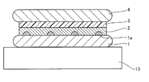
- FIG. 4 is a schematic cross-sectional view of another example of a laminate
- FIG. 1 is a diagram (part 1) for explaining one aspect of manufacturing a laminated body and manufacturing a thin wafer
- FIG. 10 is a diagram (part 2) for explaining one aspect of manufacturing a laminated body and manufacturing a thinned wafer
- FIG. 3 is a diagram (part 3) for explaining one aspect of manufacturing a laminated body and manufacturing a thinned wafer
- FIG. 4 is a diagram (part 4) for explaining one aspect of manufacturing a laminated body and manufacturing a thinned wafer
- FIG. 5 is a diagram (No. 5) for explaining one aspect of manufacturing a laminated body and manufacturing a thinned wafer
- FIG. 6 is a diagram (No. 6) for explaining one aspect of manufacturing a laminated body and manufacturing a thinned wafer;
- the adhesive composition of the present invention is a composition that can be suitably used to form an adhesive layer for temporary adhesion for processing semiconductor substrates.
- the adhesive composition of the present invention contains an adhesive component (S).
- the adhesive component (S) contains a polyorganosiloxane component (A) that cures through a hydrosilylation reaction.
- the polyorganosiloxane component (A) contains a polymer (V) represented by the following formula (V) and having a weight average molecular weight of 60,000 or more. (n indicates the number of repeating units and is a positive integer.)
- the adhesive composition of the present invention preferably contains an adhesive component (S) and, in addition to the adhesive component (S), a release agent component (B) containing polyorganosiloxane.
- the adhesive composition of the present invention may contain other components such as a solvent in order to adjust the viscosity of the adhesive composition. may contain.
- the adhesive composition of the present invention is capable of suppressing deformation of bumps and forming an adhesive layer exhibiting a high etching rate.
- the adhesive component contains a polyorganosiloxane component (A) that cures through a hydrosilylation reaction.
- the polyorganosiloxane component ( A ) includes siloxane units ( Q units) represented by SiO 2 and siloxane units ( M units), siloxane units represented by R 4 R 5 SiO 2/2 (D units), and siloxane units represented by R 6 SiO 3/2 (T units). It contains a polyorganosiloxane (A1) containing units of and a platinum group metal-based catalyst (A2).
- the polyorganosiloxane (A1) is a siloxane unit (Q' unit) represented by SiO 2 , a siloxane unit (M' unit) represented by R 1 'R 2 'R 3 'SiO 1/2 , R 1 or 2 selected from the group consisting of siloxane units represented by 4′R 5′SiO 2/2 (D′ units) and siloxane units represented by R 6′SiO 3/2 (T′ units)
- Polyorganosiloxane (a1) containing the above units and containing at least one selected from the group consisting of M' units, D' units and T' units, and a siloxane unit (Q" unit) represented by SiO 2 , R 1 ′′R 2 ′′R 3 ′′SiO 1/2 siloxane units (M′′ units), R 4 ′′R 5 ′′SiO 2/2 siloxane units (D′′ units), and R 6 Contains one or more units selected from the group consisting of siloxane units (T"
- R 1 to R 6 are groups or atoms bonded to a silicon atom and each independently represents an optionally substituted alkyl group, an optionally substituted alkenyl group or a hydrogen atom.
- substituents include halogen atoms, nitro groups, cyano groups, amino groups, hydroxy groups, carboxyl groups, aryl groups, heteroaryl groups and the like.
- R 1 ' to R 6 ' are groups bonded to a silicon atom and each independently represents an optionally substituted alkyl group or an optionally substituted alkenyl group, and R 1 ' to R 6 At least one of ' is an optionally substituted alkenyl group.
- substituents include halogen atoms, nitro groups, cyano groups, amino groups, hydroxy groups, carboxyl groups, aryl groups, heteroaryl groups and the like.
- R 1 ′′ to R 6 ′′ are groups or atoms bonded to a silicon atom and each independently represent an optionally substituted alkyl group or hydrogen atom, but at least one of R 1 ′′ to R 6 ′′ One is a hydrogen atom.
- substituents include halogen atoms, nitro groups, cyano groups, amino groups, hydroxy groups, carboxyl groups, aryl groups, heteroaryl groups and the like.
- the alkyl group may be linear, branched or cyclic, but is preferably a linear or branched alkyl group. Yes, preferably 30 or less, more preferably 20 or less, and even more preferably 10 or less.
- optionally substituted linear or branched alkyl groups include methyl, ethyl, n-propyl, i-propyl, n-butyl, i-butyl and s-butyl. group, tertiary butyl group, n-pentyl group, 1-methyl-n-butyl group, 2-methyl-n-butyl group, 3-methyl-n-butyl group, 1,1-dimethyl-n-propyl group, 1,2-dimethyl-n-propyl group, 2,2-dimethyl-n-propyl group, 1-ethyl-n-propyl group, n-hexyl group, 1-methyl-n-pentyl group, 2-methyl-n -pentyl group, 3-methyl-n-pentyl group, 4-methyl-n-pentyl group, 1,1-dimethyl-n-butyl group, 1,2-dimethyl-n-butyl group, 1,3-dimethyl- n-
- optionally substituted cyclic alkyl groups include a cyclopropyl group, a cyclobutyl group, a 1-methyl-cyclopropyl group, a 2-methyl-cyclopropyl group, a cyclopentyl group, a 1-methyl-cyclobutyl group, a 2- methyl-cyclobutyl group, 3-methyl-cyclobutyl group, 1,2-dimethyl-cyclopropyl group, 2,3-dimethyl-cyclopropyl group, 1-ethyl-cyclopropyl group, 2-ethyl-cyclopropyl group, cyclohexyl group , 1-methyl-cyclopentyl group, 2-methyl-cyclopentyl group, 3-methyl-cyclopentyl group, 1-ethyl-cyclobutyl group, 2-ethyl-cyclobutyl group, 3-ethyl-cyclobutyl group, 1,2-dimethyl-cyclobutyl group, 1,3-dimethyl-cycl
- the alkenyl group may be linear or branched, and the number of carbon atoms thereof is not particularly limited, but is usually 2 to 40, preferably 30 or less, more preferably 20 or less, and more preferably 20 or less. It is preferably 10 or less.
- optionally substituted linear or branched alkenyl groups include, but are not limited to, vinyl groups, allyl groups, butenyl groups, pentenyl groups, and the like. 2 to 14, preferably 2 to 10, more preferably 1 to 6. Among them, an ethenyl group and a 2-propenyl group are particularly preferred.
- Specific examples of the optionally substituted cyclic alkenyl group include, but are not limited to, cyclopentenyl, cyclohexenyl and the like, and the number of carbon atoms thereof is usually 4 to 14, preferably 5 to 10, More preferably 5-6.
- polyorganosiloxane (A1) includes polyorganosiloxane (a1) and polyorganosiloxane (a2), but the alkenyl group contained in polyorganosiloxane (a1) and the polyorganosiloxane (a2) contain A hydrogen atom (Si—H group) is formed and cured by forming a crosslinked structure through a hydrosilylation reaction by the platinum group metal-based catalyst (A2). As a result, a cured film is formed.
- Polyorganosiloxane (a1) contains one or more units selected from the group consisting of Q' units, M' units, D' units and T' units, and M' units, D' units and T ' contains at least one selected from the group consisting of units.
- the polyorganosiloxane (a1) two or more polyorganosiloxanes satisfying such conditions may be used in combination.
- the polymer represented by the following formula (V) is classified as polyorganosiloxane (a1) in polyorganosiloxane (A1) described above.
- the adhesive composition of the present invention contains, as an essential component, a polymer (V) represented by the following formula (V) and having a weight average molecular weight of 60,000 or more. That is, the weight-average molecular weight of the polymer represented by formula (V) contained in the adhesive composition of the present invention is 60,000 or more.
- the adhesive composition of the present invention may contain one or more polyorganosiloxanes included in the polyorganosiloxane (a1) in addition to the polymer represented by formula (V). In addition, the polymer (V) will be described in detail below. (n indicates the number of repeating units and is a positive integer.)
- Q' units, M' units, D' units and T' units include (Q' unit and M' unit), (D' unit and M' unit), (T' units and M' units), (Q' units and T' units and M' units), but are not limited to these.
- Polyorganosiloxane (a2) contains one or more units selected from the group consisting of Q′′ units, M′′ units, D′′ units and T′′ units, and M′′ units, D′′ units and T It contains at least one selected from the group consisting of "units.”
- the polyorganosiloxane (a2') two or more polyorganosiloxanes satisfying such conditions may be used in combination.
- Preferred combinations of two or more selected from the group consisting of Q′′ units, M′′ units, D′′ units and T′′ units include (M′′ units and D′′ units), (Q′′ units and M′′ units), (Q" units and T" units and M” units).
- Polyorganosiloxane ( a1 ) is composed of siloxane units in which alkyl groups and/or alkenyl groups are bonded to silicon atoms thereof, and alkenyl
- the proportion of groups is preferably 0.1 to 50.0 mol %, more preferably 0.5 to 30.0 mol %, and the remaining R 1 '-R 6 ' can be alkyl groups.
- Polyorganosiloxane (a2) is composed of siloxane units in which alkyl groups and/or hydrogen atoms are bonded to silicon atoms thereof, and all substituents and substituents represented by R 1 '' to R 6 ''
- the ratio of hydrogen atoms in the atoms is preferably 0.1 to 50.0 mol%, more preferably 10.0 to 40.0 mol%, and the remaining R 1 ′′ to R 6 ′′ are alkyl groups. be able to.
- component (A) contains (a1) and (a2)
- the alkenyl group contained in polyorganosiloxane (a1) and the Si—H bond contained in polyorganosiloxane (a2) is in the range of 1.0:0.5 to 1.0:0.66.
- Polymer (V) is represented by formula (V) and has a weight average molecular weight of 60,000 or more, more preferably 100,000 or more. Generally, its weight average molecular weight is between 60,000 and 1,000,000, more preferably between 100,000 and 1,000,000.
- the weight-average molecular weight of the polyorganosiloxane other than the polymer (V) in the polyorganosiloxane (a1) is not particularly limited, but is usually 500 to 1,000,000, and the effect of the present invention can be reproduced with good reproducibility. From the viewpoint of realization, it is preferably 5,000 to 50,000.
- the weight average molecular weight of the polyorganosiloxane (a2) is not particularly limited, it is usually 500 to 1,000,000, and preferably 5,000 to 50 from the viewpoint of achieving the effects of the present invention with good reproducibility. , 000.
- the weight-average molecular weight, number-average molecular weight and degree of dispersion of the polyorganosiloxane are determined by, for example, a GPC apparatus (EcoSEC, HLC-8320GPC manufactured by Tosoh Corporation) and a GPC column (TSKgel SuperMultiporeHZ-N manufactured by Tosoh Corporation).
- TSKgel SuperMultiporeHZ-H TSKgel SuperMultiporeHZ-H
- the column temperature was set to 40 ° C.
- tetrahydrofuran was used as the eluent (elution solvent)
- the flow rate was set to 0.35 mL / min
- polystyrene Showa Denko Co., Ltd. Shodex
- the viscosities of the polyorganosiloxane (a1) and the polyorganosiloxane (a2) are not particularly limited, but each is usually 10 to 1,000,000 (mPa s), and the effects of the present invention are realized with good reproducibility. From the point of view, it is preferably 50 to 200,000 (mPa ⁇ s).
- the viscosities of polyorganosiloxane (a1) and polyorganosiloxane (a2) are values measured at 25° C. with an E-type rotational viscometer.
- Polyorganosiloxane (a1) and polyorganosiloxane (a2) react with each other through a hydrosilylation reaction to form a cured film. Therefore, the curing mechanism differs from that via, for example, silanol groups, and therefore any siloxane need not contain silanol groups or functional groups that form silanol groups upon hydrolysis, such as alkyloxy groups. None.
- the adhesive component (S) contains a platinum group metal-based catalyst (A2) together with the polyorganosiloxane component (A1).
- a platinum-based metal catalyst is a catalyst for promoting the hydrosilylation reaction between the alkenyl groups of the polyorganosiloxane (a1) and the Si—H groups of the polyorganosiloxane (a2).
- platinum-based metal catalysts include platinum black, diplatinum chloride, chloroplatinic acid, reactants of chloroplatinic acid and monohydric alcohols, complexes of chloroplatinic acid and olefins, platinum bisacetoacetate, and the like.
- platinum-based catalysts including, but not limited to: Examples of complexes of platinum and olefins include, but are not limited to, complexes of divinyltetramethyldisiloxane and platinum.
- the amount of platinum group metal-based catalyst (A2) is not particularly limited, but is usually in the range of 1.0 to 50.0 ppm with respect to the total amount of polyorganosiloxane (a1) and polyorganosiloxane (a2). .
- the polyorganosiloxane component (A) may contain a polymerization inhibitor (A3) for the purpose of suppressing the progress of the hydrosilylation reaction.
- the polymerization inhibitor is not particularly limited as long as it can suppress the progress of the hydrosilylation reaction, and specific examples thereof include 1-ethynyl-1-cyclohexanol and 1,1-diphenyl-2-propion-1-ol.
- the amount of the polymerization inhibitor is not particularly limited, it is usually 1000.0 ppm or more with respect to the total amount of the polyorganosiloxane (a1) and the polyorganosiloxane (a2) from the viewpoint of obtaining the effect, and the hydrosilylation reaction It is 10000.0 ppm or less from the viewpoint of preventing excessive suppression of.
- the adhesive composition of the present invention is represented by the following formula (V) as the aforementioned polyorganosiloxane (a1) constituting the polyorganosiloxane component (A) that cures by a hydrosilylation reaction, and has a weight average molecular weight of 60, 000 or more of the polymer (V).
- the polymer represented by formula (V) may be a commercial product or a synthesized product.
- Commercially available products of the polymer represented by formula (V) include, for example, products manufactured by Wacker Chemie.
- the commercially available polymer represented by the formula (V) When the commercially available polymer represented by the formula (V) has a desired weight-average molecular weight, it may be used singly as it is. In addition, two or more polymers represented by the formula (V) having different weight average molecular weights may be used in combination. Further, when the synthesized polymer represented by the formula (V) has a desired weight-average molecular weight, it may be used alone as it is, and the weight-average molecular weight has a desired value. As in the above, two or more polymers represented by formula (V) having different weight-average molecular weights and synthesized separately may be used in combination. Furthermore, a commercially available product and a synthesized product may be used in combination.
- the weight average molecular weight of polymer (V) is preferably 100,000 or more. That is, by using the adhesive composition containing the polymer (V) represented by the formula (V) and having a weight average molecular weight of 100,000 or more, a more excellent bump deformation suppressing effect and a higher etching An adhesive layer showing a rate can be formed with good reproducibility. From the viewpoint of exhibiting both a good bump deformation suppressing effect and a high etching rate in a well-balanced manner, the weight average molecular weight of the polymer (V) is preferably 160,000 or less, more preferably 150,000. 000 or less, more preferably 130,000 or less, and even more preferably 110,000 or less.
- the molecular weight distribution (Mw/Mn) of the polymer (V) determined from the weight average molecular weight (Mw) and number average molecular weight (Mn) exhibits both a good bump deformation suppressing effect and a high etching rate in a well-balanced manner. It is preferably 3.2 to 25, more preferably 3.2 to 15, and even more preferably 9 to 13, from the viewpoint that
- a polymer (V) having a weight-average molecular weight of 60,000 or more two or more polymers having different molecular weight regions included in the formula (V) are used, and these polymers are By mixing coalescence as a raw material, it is possible to prepare a polymer (V) having a desired weight-average molecular weight with good reproducibility.
- the following method can be mentioned as a method of obtaining a polymer (V).
- the polymer (V) obtained by the method (ib) above When the polymer (V) obtained by the method (ib) above is used, a more excellent effect of suppressing bump deformation is exhibited than when the polymer (V) obtained by the method (ia) is used.
- the adhesive layer can be formed with good reproducibility.
- a polymer (V) having a weight average molecular weight of 100,000 to 130,000 can be obtained with good reproducibility.
- the effect of suppressing bump deformation is more excellent than when the polymer (V) obtained by the method (ia) is used.
- An adhesive layer exhibiting a high etching rate can be formed with good reproducibility.
- the following method can be mentioned as a more specific method of the above method (i).
- a polymer (V) having a weight average molecular weight of 60,000 or more can be obtained.
- the following method can be mentioned as a more preferred embodiment of the method for obtaining the polymer (V).
- the polymer (V) having a weight average molecular weight of 100,000 or more can be obtained with good reproducibility.
- the polymer (V) obtained by the method (ii-b) is used, the polymer (V) obtained by the method (ii-a) exhibits a more excellent effect of suppressing bump deformation.
- the adhesive layer can be formed with better reproducibility.
- a polymer (V) having a weight average molecular weight of 100,000 to 130,000 can be obtained with good reproducibility.
- the effect of suppressing bump deformation is more excellent than when the polymer (V) obtained by the method (ii-a) is used.
- An adhesive layer exhibiting a high etching rate can be formed with better reproducibility.
- the method of mixing the polymers is not particularly limited. Determine the mixing ratio and mix the polymer well using a stirrer. At this time, if the amount of the polymer used is small, the mixture cannot be sufficiently mixed, and a highly uniform polymer cannot be obtained with good reproducibility.
- the mixing ratio for obtaining the desired weight-average molecular weight can be appropriately determined by those skilled in the art without excessive trial and error, considering the weight-average molecular weight of each polymer used.
- the weight average molecular weight of the polymer represented by the above formula (V) contained in the adhesive composition may be a desired value, the polymers represented by the above formula (V) having different molecular weight regions
- the polymers represented by the above formula (V) having different molecular weight regions
- the polymer (V) does not need to be prepared as an individual prior to its preparation.
- Two or more polymers of formula (V) that do not have may be mixed to finally achieve polymer (V) in the adhesive composition.
- the polymer (V-1) is treated with one or more formulas having different weight average molecular weights.
- a polymer (V-2), which is the polymer (V) may be obtained by mixing the polymers represented by (V).
- the object of the present invention can also be achieved by incorporating a polymer represented by formula (V), particularly a polymer having a large molecular weight of 60,000 or more in weight average molecular weight.
- a polymer represented by formula (V) particularly a polymer having a large molecular weight of 60,000 or more in weight average molecular weight.
- the polymer represented by the formula (V) has groups other than —Si(CH 3 ) 2 CHCH 2 groups and —Si(CH 3 ) 2 —O— groups at terminals and in the middle of repeating units in the bulk of the polymer. It is undeniable that there are polymers containing other groups as trace impurity structures.
- the adhesive composition of the present invention may contain a release agent component (B) containing polyorganosiloxane (hereinafter also referred to as component (B)) in addition to the adhesive component (S) described above.
- the adhesive composition of the present invention includes, as the adhesive component (S), a polyorganosiloxane component (A) (hereinafter also referred to as component (A)), which is a curing component, and a release agent component. It contains a component (B) that does not cause a curing reaction.
- a release agent component (B) typically includes polyorganosiloxanes, and specific examples thereof include epoxy group-containing polyorganosiloxanes, methyl group-containing polyorganosiloxanes, phenyl group-containing polyorganosiloxanes, and the like. include, but are not limited to.
- a polydimethylsiloxane is mentioned as a release agent component (B).
- the polydimethylsiloxane may be modified.
- examples of polydimethylsiloxane that may be modified include, but are not limited to, epoxy group-containing polydimethylsiloxane, unmodified polydimethylsiloxane, and phenyl group-containing polydimethylsiloxane.
- the weight-average molecular weight of the polyorganosiloxane that is the release agent component (B) is not particularly limited, it is usually from 100,000 to 2,000,000. 200,000 to 1,200,000, more preferably 300,000 to 900,000.
- the degree of dispersion (Mw/Mn) is not particularly limited, but is usually 1.0 to 10.0, and preferably 1.5 to 5.0 from the viewpoint of realizing suitable peeling with good reproducibility. , more preferably 2.0 to 3.0.
- the weight-average molecular weight and degree of dispersion can be measured by the methods described above for polyorganosiloxane.
- epoxy group-containing polyorganosiloxanes examples include those containing siloxane units ( D10 units) represented by R 11 R 12 SiO 2/2 .
- R 11 is a group bonded to a silicon atom and represents an alkyl group
- R 12 is a group bonded to a silicon atom and represents an epoxy group or an organic group containing an epoxy group
- specific examples of the alkyl group are , the aforementioned examples can be mentioned.
- the epoxy group in the organic group containing an epoxy group may be an independent epoxy group without being condensed with other rings, and forms a condensed ring with other rings such as a 1,2-epoxycyclohexyl group. may be an epoxy group.
- Specific examples of organic groups containing epoxy groups include, but are not limited to, 3-glycidoxypropyl and 2-(3,4-epoxycyclohexyl)ethyl.
- a preferable example of the epoxy group-containing polyorganosiloxane is epoxy group-containing polydimethylsiloxane, but the present invention is not limited thereto.
- the epoxy group-containing polyorganosiloxane contains the aforementioned siloxane units ( D10 units), but may contain Q units, M units and/or T units in addition to the D10 units.
- specific examples of the epoxy group-containing polyorganosiloxane include a polyorganosiloxane consisting only of D10 units, a polyorganosiloxane containing D10 units and Q units, and a polyorganosiloxane containing D10 units and M units.
- Polyorganosiloxane containing D10 units and T units Polyorganosiloxane containing D10 units, Q units and M units Polyorganosiloxane containing D10 units, M units and T units , polyorganosiloxanes containing D 10 units, Q units, M units and T units.
- Epoxy group-containing polyorganosiloxane is preferably epoxy group-containing polydimethylsiloxane having an epoxy value of 0.1 to 5.
- the weight average molecular weight is not particularly limited, it is usually 1,500 to 500,000, and preferably 100,000 or less from the viewpoint of suppressing deposition in the adhesive.
- epoxy group-containing polyorganosiloxanes include those represented by formulas (E1) to (E3), but are not limited to these.
- methyl group-containing polyorganosiloxane for example, one containing a siloxane unit ( D200 unit) represented by R210R220SiO2 / 2 , preferably a siloxane unit represented by R21R21SiO2 /2 (D 20 units).
- R 210 and R 220 are groups bonded to a silicon atom, each independently representing an alkyl group, at least one of which is a methyl group, and specific examples of the alkyl group are the aforementioned examples.
- R 21 is a group bonded to a silicon atom and represents an alkyl group, and specific examples of the alkyl group include those mentioned above. Among them, R 21 is preferably a methyl group.
- a preferred example of the methyl group-containing polyorganosiloxane is polydimethylsiloxane, but the present invention is not limited thereto.
- Methyl group-containing polyorganosiloxane contains the above-mentioned siloxane units (D 200 units or D 20 units), but in addition to D 200 units and D 20 units, it may contain Q units, M units and / or T units. .
- methyl group-containing polyorganosiloxane examples include a polyorganosiloxane consisting only of D 200 units, a polyorganosiloxane containing D 200 units and Q units, and a polyorganosiloxane containing D 200 units and M units.
- polyorganosiloxane containing D 200 units and T units polyorganosiloxane containing D 200 units, Q units and M units
- polyorganosiloxane containing D 200 units, M units and T units D 200 units, Q units, M units and T units.
- methyl group-containing polyorganosiloxane examples include polyorganosiloxane consisting only of D20 units, polyorganosiloxane containing D20 units and Q units, and polyorganosiloxane containing D20 units and M units.
- polyorganosiloxane containing D20 units and T units polyorganosiloxane containing D20 units Q units and M units polyorganosiloxane containing D20 units M units T units , D 20 units, Q units, M units and T units.
- methyl group-containing polyorganosiloxane examples include, but are not limited to, those represented by the formula (M1).
- n4 indicates the number of repeating units and is a positive integer.
- phenyl group-containing polyorganosiloxanes examples include those containing siloxane units (D 30 units) represented by R 31 R 32 SiO 2/2 .
- R 31 is a group bonded to a silicon atom and represents a phenyl group or an alkyl group
- R 32 is a group bonded to a silicon atom and represents a phenyl group; can be mentioned, but a methyl group is preferred.
- the phenyl group-containing polyorganosiloxane contains the aforementioned siloxane units ( D30 units), but may contain Q units, M units and/or T units in addition to the D30 units.
- phenyl group-containing polyorganosiloxane examples include a polyorganosiloxane consisting only of D30 units, a polyorganosiloxane containing D30 units and Q units, and a polyorganosiloxane containing D30 units and M units.
- polyorganosiloxane containing D 30 units and T units polyorganosiloxane containing D 30 units Q units and M units polyorganosiloxane containing D 30 units M units T units , D 30 units, Q units, M units and T units.
- phenyl group-containing polyorganosiloxane examples include, but are not limited to, those represented by formula (P1) or (P2).
- Polyorganosiloxane which is the release agent component (B), may be a commercially available product or a synthesized product.
- Commercially available products of polyorganosiloxane include, for example, WACKERSILICONE FLUID AK series (AK50, AK 350, AK 1000, AK 10000, AK 1000000) manufactured by Wacker Chemi Co., Ltd., GENIOPLAST GUM, and dimethyl silicone manufactured by Shin-Etsu Chemical Co., Ltd.
- phenyl group-containing polyorganosiloxane (PMM-1043, PMM-1025, PDM-0421, PDM-0821), Shin-Etsu Chemical Co., Ltd.
- phenyl group-containing polyorganosiloxane Examples include siloxane (KF50-3000CS), phenyl group-containing polyorganosiloxane (TSF431, TSF433) manufactured by Momentive, but not limited thereto.
- the adhesive composition of the present invention comprises an adhesive component (S) and a release agent component (B) containing polyorganosiloxane that does not undergo a curing reaction.
- an adhesive composition containing, as the release agent component (B), a release agent component (H) containing a polyorganosiloxane having a complex viscosity of 3400 (Pa ⁇ s) or more is more preferable.
- the complex viscosity of polyorganosiloxane, which is the release agent component (H) means a value measured at 25° C. using a rheometer.
- the adhesive composition of the present invention is preferably an adhesive composition containing a release agent component (H) as the release agent component (B). ) can contain one or more of the release agent components included in ).
- the complex viscosity of the polyorganosiloxane that is the release agent component (H) is, as described above, 3400 (Pa ⁇ s) or more, but from the viewpoint of realizing the effects of the present invention with good reproducibility, it is preferably 4000 (Pa s) or more, more preferably 4,500 (Pa s) or more, still more preferably 5,000 (Pa s) or more, and still more preferably 5,500 (Pa s) or more, and the organic solvent is used to prepare the adhesive composition.
- the adhesive composition of the present invention may contain a solvent for the purpose of adjusting the viscosity, etc.
- a solvent for the purpose of adjusting the viscosity, etc.
- Specific examples of the solvent include aliphatic hydrocarbons, aromatic hydrocarbons, ketones and the like. is not limited to
- the solvent includes hexane, heptane, octane, nonane, decane, undecane, dodecane, isododecane, menthane, limonene, toluene, xylene, mesitylene, cumene, MIBK (methyl isobutyl ketone), butyl acetate, and diisobutyl.
- examples include, but are not limited to, ketones, 2-octanone, 2-nonanone, 5-nonanone, and the like. Such solvents can be used singly or in combination of two or more.
- the adhesive composition of the present invention contains a solvent
- the content thereof is appropriately determined in consideration of the viscosity of the desired composition, the coating method to be employed, the thickness of the film to be produced, etc.
- the composition It is in the range of about 10 to 90% by mass with respect to the entire product.
- the viscosity of the adhesive composition of the present invention is not particularly limited, it is usually 500 to 20,000 mPa ⁇ s, preferably 1,000 to 6,000 mPa ⁇ s at 25°C.
- the viscosity of the adhesive composition of the present invention can be adjusted by considering various factors such as the coating method used and the desired film thickness, and changing the types of solvents to be used, their ratios, the concentrations of film constituents, and the like. be.
- the film-constituting component means a component other than the solvent contained in the composition.
- the adhesive composition of the present invention can be prepared by mixing the adhesive component (S), the release agent component (B), and, if used, a solvent. can be manufactured.
- the mixing order is not particularly limited, but as an example of a method for easily and reproducibly producing the adhesive composition of the present invention, for example, an adhesive component (S) and a release agent component (B) are mixed together. in a solvent, and a method of dissolving a part of the adhesive component (S) and the release agent component (B) in a solvent, dissolving the rest in a solvent, and mixing the resulting solutions. It is not limited to these.
- the adhesive composition when preparing the adhesive composition, it may be appropriately heated within a range in which the components are not decomposed or deteriorated.
- the adhesive composition for the purpose of removing foreign matter, the adhesive composition may be filtered using a filter or the like during the production of the adhesive composition or after all the components are mixed.
- a laminate of the present invention includes a semiconductor substrate with bumps, a support substrate, and an adhesive layer.
- the adhesive layer is interposed between the semiconductor substrate with bumps and the support substrate and contacts the semiconductor substrate.
- the adhesive layer is a layer formed from the adhesive composition of the present invention described above.
- the laminated body is used for temporary adhesion for processing a semiconductor substrate, and can be suitably used for applications in which the support substrate and the semiconductor substrate are separated after processing the semiconductor substrate in the laminated body.
- the number of adhesive layers is not particularly limited and is appropriately selected according to the purpose.
- the laminate may have one adhesive layer or two or more adhesive layers.
- the laminate of the present invention may contain a layer other than an adhesive layer between the semiconductor substrate and the supporting substrate, and examples thereof include a laminate including an adhesive layer and a release layer between the semiconductor substrate and the supporting substrate.
- a preferred embodiment of the laminate of the present invention is a laminate having a semiconductor substrate, an adhesive layer, a release layer, and a support substrate in this order.
- the laminate of the present invention has an adhesive layer that can suitably temporarily bond a semiconductor substrate with bumps and a support substrate, can suppress or alleviate bump deformation due to external loads such as heating, and exhibits a high etching rate. ing. Therefore, the laminate of the present invention is a laminate having an adhesive layer that satisfies both the effect of suppressing bump deformation and a high etching rate.
- FIG. 1A is a schematic cross-sectional view of an example of a laminate.
- the laminate of FIG. 1A has a semiconductor substrate 1 having bumps 1a, an adhesive layer 2, and a support substrate 4 in this order.
- the bumps 1a of the semiconductor substrate 1 are arranged on the support substrate 4 side.
- the adhesive layer 2 is interposed between the semiconductor substrate 1 and the support substrate 4 .
- the adhesive layer 2 is in contact with the semiconductor substrate 1 .
- the adhesive layer 2 covers the bumps 1a.
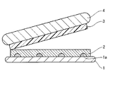
- FIG. 1B is a schematic cross-sectional view of another example of the laminate.
- the laminate of FIG. 1B has a semiconductor substrate 1 having bumps 1a, an adhesive layer 2, a release layer 3, and a support substrate 4 in this order.
- the bumps 1a of the semiconductor substrate 1 are arranged on the support substrate 4 side.
- the adhesive layer 2 is interposed between the semiconductor substrate 1 and the support substrate 4 .
- the adhesive layer 2 is in contact with the semiconductor substrate 1 .
- the adhesive layer 2 covers the bumps 1a.
- the release layer 3 is interposed between the adhesive layer 2 and the support substrate 4 .
- the release layer 3 is in contact with the adhesive layer 2 and the support substrate 4 .
- the semiconductor substrate has bumps.
- a bump is a projecting terminal.
- the semiconductor substrate has bumps on the support substrate side.
- bumps are usually formed on the surface on which circuits are formed.
- the circuit may be a single layer or multiple layers.
- the shape of the circuit is not particularly limited.
- the surface opposite to the surface having the bumps (back surface) is a surface to be processed.
- the main material that constitutes the entire semiconductor substrate is not particularly limited as long as it is used for this type of application, and examples thereof include silicon, silicon carbide, compound semiconductors, and the like.
- the shape of the semiconductor substrate is not particularly limited, but is, for example, a disc shape. It should be noted that the disk-shaped semiconductor substrate does not need to have a perfectly circular surface shape. It may have notches.
- the thickness of the disk-shaped semiconductor substrate may be appropriately determined according to the purpose of use of the semiconductor substrate, and is not particularly limited, but is, for example, 500 to 1,000 ⁇ m.
- the diameter of the disk-shaped semiconductor substrate may be appropriately determined depending on the purpose of use of the semiconductor substrate, and is not particularly limited.
- An example of a semiconductor substrate is a silicon wafer with a diameter of 300 mm and a thickness of about 770 ⁇ m.
- the material, size, shape, structure, and density of the bumps on the semiconductor substrate are not particularly limited.
- bumps include ball bumps, printed bumps, stud bumps, and plated bumps.
- the height, diameter and pitch of bumps are appropriately determined from the conditions of a bump height of about 1 to 200 ⁇ m, a bump diameter of 1 to 200 ⁇ m, and a bump pitch of 1 to 500 ⁇ m.
- Materials for the bumps include, for example, low-melting solder, high-melting solder, tin, indium, gold, silver, and copper.
- the bumps may consist of only a single component, or may consist of multiple components.
- Sn-based alloy plating such as SnAg bumps, SnBi bumps, Sn bumps, and AuSn bumps can be used.
- the bump may have a laminated structure including a metal layer composed of at least one of these components.
- the support substrate is not particularly limited as long as it is a member capable of supporting the semiconductor substrate when the semiconductor substrate is processed. Examples thereof include a glass support substrate and a silicon support substrate.
- the shape of the support substrate is not particularly limited, but for example, a disk shape can be mentioned. It should be noted that the disc-shaped support substrate does not need to have a perfectly circular surface shape. It may have notches.
- the thickness of the disc-shaped support substrate may be appropriately determined according to the size of the semiconductor substrate, and is not particularly limited, but is, for example, 500 to 1,000 ⁇ m.
- the diameter of the disk-shaped support substrate may be appropriately determined according to the size of the semiconductor substrate, and is not particularly limited, but is, for example, 100 to 1,000 mm.
- the support substrate is a glass wafer or silicon wafer with a diameter of 300 mm and a thickness of about 700 ⁇ mm.
- the laminate includes a peeling layer and light for peeling the peeling layer is irradiated from the supporting substrate side
- a supporting substrate that transmits light is used.
- the light transmittance is usually 50% or higher, preferably 80% or higher, more preferably 90% or higher.
- a support substrate made of glass can be used, but it is not limited to this.
- the adhesive layer is interposed between the support substrate and the semiconductor substrate.
- the adhesive layer contacts the semiconductor substrate.
- the adhesive layer is formed using the adhesive composition of the present invention described above, more specifically, by curing the adhesive composition.
- the thickness of the adhesive layer is not particularly limited, it is preferably 20 to 120 ⁇ m, more preferably 40 to 100 ⁇ m from the viewpoint of obtaining a good bump deformation suppressing effect.
- the method for forming the adhesive layer from the adhesive composition will be described in detail in the description of ⁇ Method for producing laminate> below.
- the laminate of the present invention may have a release layer.
- the release layer can be arranged so as to be in contact with the supporting substrate and the adhesive layer.
- the type of the peeling layer and the peeling method are not particularly limited.
- a release layer as described below can be used.
- the release layer is a film obtained from a release agent composition containing an organic resin and a solvent.
- the film is a cured film obtained by curing the film constituents in the release agent composition.
- the release agent composition can further include a cross-linking agent, an acid catalyst, and a surfactant.
- the release agent composition contains an organic resin.
- Such an organic resin is preferably one that exhibits suitable peeling ability. Alteration necessary for improvement, such as decomposition, preferably occurs.
- a preferred example of the organic resin is a novolac resin.
- a novolac resin that absorbs light with a wavelength of 190 nm to 600 nm and deteriorates is preferable, and a light such as a laser with a wavelength of 308 nm, 343 nm, 355 nm or 365 nm.
- a novolak resin that is modified by irradiation of is more preferable.
- the novolac resin is represented by a unit represented by the following formula (C1-1), a unit represented by the following formula (C1-2), and a unit represented by the following formula (C1-3). It is a polymer containing one or more selected from the group consisting of units.
- C1 represents a group derived from an aromatic compound containing a nitrogen atom
- C2 is a secondary carbon atom, a quaternary carbon atom and at least one selected from the group consisting of an aromatic ring in the side chain represents a group containing a tertiary carbon atom
- C3 represents a group derived from an aliphatic polycyclic compound
- C4 represents a group derived from phenol, a group derived from bisphenol, a group derived from naphthol, a group derived from biphenyl group or a group derived from biphenol.
- the novolak resin to be contained in the release agent composition and the release layer using the novolak resin, reference can be made to the novolak resin described in WO 2019/088103 and the release layer using the novolak resin.
- the release layer is formed by applying a release agent composition, drying, and curing.
- the thickness of the release layer provided in the laminate according to the present invention is appropriately set in consideration of the type of the release agent component, the desired degree of release property, etc., but is usually 5 to 10,000 nm. It is preferably 10 nm or more, more preferably 50 nm or more, and even more preferably 100 nm or more, from the viewpoint of suppressing deterioration of peelability due to a thin film and obtaining a peeling layer with excellent peelability with good reproducibility. From the viewpoint of avoiding the properties, the thickness is preferably 5,000 nm or less, more preferably 1,000 nm or less, and even more preferably 500 nm or less.
- the method for producing the laminate of the present invention includes the step of forming the adhesive layer (adhesion agent coating layer forming step and adhesive layer forming step) and, if necessary, other steps such as a bonding step.
- a method for producing a laminate in this case will be described in detail in the section ⁇ first embodiment>> below.
- the method for producing the laminate of the present invention includes the step of forming the adhesive layer (adhesive coating layer forming step and adhesive layer forming step), A step of forming a release layer is included, and, if necessary, other steps such as a bonding step are included.
- the method for manufacturing the laminate in this case will be described in detail in the section ⁇ second embodiment>> below.
- An adhesive layer is formed through an adhesive coating layer forming step and an adhesive layer forming step.
- an adhesive composition is applied to a semiconductor substrate with bumps to form an adhesive coating layer.
- the coating method is not particularly limited, it is usually a spin coating method.
- a method of separately forming a coating film by a spin coating method or the like and sticking the sheet-like coating film as an adhesive coating layer can be adopted.
- the thickness of the adhesive coating layer is appropriately determined in consideration of the thickness of the adhesive layer in the laminate. For the reason that the adhesive composition contains a solvent or the like, the applied adhesive composition may be heated for the purpose of drying the coating film of the applied adhesive composition (preheat treatment).
- the heating temperature of the applied adhesive composition varies depending on the type and amount of the adhesive component contained in the adhesive composition, whether or not a solvent is contained, the boiling point of the solvent used, the desired thickness of the adhesive layer, and the like. Therefore, it cannot be defined unconditionally, but it is usually 80 to 150° C. and the heating time is usually 30 seconds to 5 minutes. Heating can be performed using a hot plate, an oven, or the like.
- the adhesive coating layer is heated to cure the adhesive composition to form an adhesive layer.
- the adhesive layer forming step is a step in which the adhesive layer is formed by heating the adhesive layer while the supporting substrate and the adhesive layer are in contact with each other and the adhesive layer and the semiconductor substrate are in contact with each other. Not limited. For example, by using a semiconductor substrate on which an adhesive coating layer is formed and a supporting substrate, and disposing the two substrates (semiconductor substrate and supporting substrate) so as to sandwich the adhesive coating layer, the supporting substrate and the adhesive are applied. After the layers are brought into contact with each other and the adhesive coating layer and the semiconductor substrate are brought into contact with each other, heat treatment may be performed (post-heat treatment).
- the heating temperature and time are not particularly limited as long as the temperature and time are such that the adhesive coating layer is converted into the adhesive layer.
- the heating temperature is preferably 120° C. or higher, more preferably 150° C. or higher, from the viewpoint of achieving a sufficient curing speed, etc., and prevents deterioration of each layer (including the support substrate and the semiconductor substrate) constituting the laminate. From the viewpoint of prevention, etc., the temperature is preferably 250° C. or less. More preferably, it is 180 to 200°C.
- the heating time is preferably 1 minute or more, more preferably 5 minutes or more, from the viewpoint of realizing suitable bonding of each layer (including the support substrate and the semiconductor substrate) constituting the laminate.
- the time is preferably 180 minutes or less, more preferably 120 minutes or less. More preferably, it is 1 to 20 minutes from the viewpoint of substrate processing efficiency. Heating can be performed using a hot plate, an oven, or the like.
- a bonding step is preferably performed between the adhesive coating layer forming step and the adhesive layer forming step in order to ensure sufficient bonding between the semiconductor substrate and the support substrate.
- the bonding process is not particularly limited as long as the substrate and the layer can be bonded together and the substrate and the layer are not damaged. can be applied, and more preferably, a load can be applied in the thickness direction of the supporting substrate and the semiconductor substrate under reduced pressure.
- the load is not particularly limited as long as the substrate and layer can be bonded together and the substrate and layer are not damaged.
- the degree of reduced pressure is not particularly limited as long as the substrate and layer can be bonded together and the substrate and layer are not damaged.
- a method for producing a laminate including a release layer As a preferred embodiment of the method for producing a laminate including a release layer, a method for producing a laminate will be described below, taking as an example the case where a release layer made of a release agent composition containing an organic resin such as the novolac resin described above is used. do.
- An adhesive coating layer is formed on the semiconductor substrate by the same method as described in the adhesive coating layer forming step column of ⁇ first embodiment>> above.
- a release agent composition is applied on a support substrate to form a release agent coating layer, which is then heated and cured to form a release layer.
- the coating method of the release agent composition the same coating method as the coating method described in the section of the step of forming the adhesive coating layer in ⁇ first embodiment>> can be used.
- the heating temperature and time are not particularly limited as long as the temperature and time are such that the adhesive coating layer is converted into the adhesive layer.
- the same conditions as those described in the adhesive layer forming step of ⁇ first embodiment>> can be used.
- a bonding step is preferably performed between the adhesive coating layer forming step and the adhesive layer forming step in order to ensure sufficient bonding between the semiconductor substrate and the supporting substrate.
- the same conditions as described in the above ⁇ first embodiment>> can be used.
- the laminate of the present invention is used for temporary bonding for processing semiconductor substrates, and can be suitably used for applications in which a support substrate and a semiconductor substrate are separated after processing the semiconductor substrate in the laminate.
- the method for manufacturing a semiconductor substrate of the present invention includes at least a processing step of processing the semiconductor substrate and a peeling step of separating the support substrate from the processed semiconductor substrate. including the steps of
- the processing step is not particularly limited as long as it is a step for processing the semiconductor substrate in the laminate according to the present invention.
- the processing step is not particularly limited as long as it is a step for processing the semiconductor substrate in the laminate according to the present invention.
- various processing steps there are cases where processing is performed under high temperature and high pressure. can be effectively prevented.
- the polishing treatment is not particularly limited as long as it is a treatment for thinning the semiconductor substrate by polishing the surface of the semiconductor substrate opposite to the surface on which the bumps are present. polishing and the like.
- the polishing process can be performed using a general polishing apparatus used for polishing semiconductor substrates.
- the polishing process reduces the thickness of the semiconductor substrate to obtain a thinned semiconductor substrate to a desired thickness.
- the thickness of the thinned semiconductor substrate is not particularly limited, but may be, for example, 30 to 300 ⁇ m or 30 to 100 ⁇ m.
- the polished semiconductor substrate is formed with a through electrode for achieving conduction between the thinned semiconductor substrates when a plurality of thinned semiconductor substrates are stacked. Therefore, the method for manufacturing a semiconductor substrate may include a through electrode forming process for forming through electrodes in the polished semiconductor substrate after the polishing process and before the peeling process.
- the method of forming the through electrode in the semiconductor substrate is not particularly limited, but examples include forming a through hole and filling the formed through hole with a conductive material. Formation of the through holes is performed, for example, by photolithography. Filling of the through-holes with a conductive material is performed by, for example, a plating technique.
- the peeling step is not particularly limited as long as it is a step in which the supporting substrate and the processed semiconductor substrate are separated after the processing step.
- Examples thereof include solvent peeling, peeling by light irradiation (laser light, non-laser light), mechanical peeling using a device having a sharp portion (so-called debonder), manual peeling between the support and the wafer, and the like. but not limited to these.
- peeling is carried out after manufacturing the laminate of the present invention and subjecting it to predetermined processing and the like.
- the laminate includes a peeling layer
- the peeling layer is formed using an organic resin that absorbs light and undergoes the alteration necessary to improve the peelability as described above.
- the release layer can be peeled off by irradiating a laser from the support side.
- the wavelength of the laser light is 190 nm to 400 nm, or ultraviolet light with a wavelength of 190 nm to 600 nm (eg, 308 nm, 355 nm, 532 nm) is used.
- the peeling can be performed by setting the processing energy density of the pulse laser to about 50 to 500 mJ/cm 2 .
- the release usually occurs within the release layer or at the interface between the release layer and an adjacent substrate or layer (eg, adhesive layer).
- the phrase "peeling occurs inside the release layer" means that the release layer is cleaved.
- the removing step is not particularly limited as long as the adhesive layer is removed after the peeling step, but an example thereof includes a method of dissolving and removing the adhesive layer using a cleaning composition.
- dissolution removal may be combined with removal using a removal tape or the like.
- a cleaning composition for example, a semiconductor substrate with an adhesive layer can be immersed in the cleaning composition or sprayed with the cleaning composition. Since the adhesive formed from the adhesive composition of the present invention exhibits a high etching rate as shown in the following examples, the laminate of the present invention is an adhesive layer left on the semiconductor substrate after the peeling step. can be easily dissolved and removed.
- a suitable example of the cleaning composition used in the present invention is a cleaning composition containing a quaternary ammonium salt and a solvent.
- the quaternary ammonium salt is composed of a quaternary ammonium cation and an anion, and is not particularly limited as long as it can be used for this type of application.
- Such quaternary ammonium cations typically include tetra(hydrocarbon)ammonium cations.
- hydroxide ions OH ⁇
- halogen ions such as fluorine ions (F ⁇ ), chloride ions (Cl ⁇ ), bromide ions (Br ⁇ ), iodine ions (I ⁇ ), etc.
- tetrafluoroborate ion BF 4 ⁇
- PF 6 ⁇ hexafluorophosphate ion
- the quaternary ammonium salt is preferably a halogen-containing quaternary ammonium salt, more preferably a fluorine-containing quaternary ammonium salt.
- the halogen atom may be contained in the cation or the anion, preferably the anion.
- the fluorine-containing quaternary ammonium salt is tetra(hydrocarbon)ammonium fluoride.
- the hydrocarbon group in the tetra(hydrocarbon)ammonium fluoride include an alkyl group having 1 to 20 carbon atoms, an alkenyl group having 2 to 20 carbon atoms, an alkynyl group having 2 to 20 carbon atoms, and an alkynyl group having 6 to 20 carbon atoms. and the like.
- the tetra(hydrocarbon)ammonium fluoride comprises a tetraalkylammonium fluoride.
- tetraalkylammonium fluoride examples include tetramethylammonium fluoride, tetraethylammonium fluoride, tetrapropylammonium fluoride, tetrabutylammonium fluoride (also referred to as tetrabutylammonium fluoride) and the like. Not limited. Among them, tetrabutylammonium fluoride is preferred.
- FIGS. 2A to 2F are diagrams for explaining one aspect of manufacturing a laminate and manufacturing a thin wafer.
- a wafer 1 having bumps 1a is prepared (FIG. 2A).
- the surface of the wafer 1 on which the bumps 1a are present is coated with an adhesive composition by spin coating using a coating device 12 to form an adhesive coating layer 2a (FIG. 2B).
- a release agent composition is applied onto the support substrate 4 by spin coating using a coating device (not shown), and the release agent composition is heated to cure to form a release layer 3, whereby the release layer 3 is formed.
- a formed support substrate 4 is prepared (FIG. 2C).
- the wafer 1 having the adhesive coating layer 2a formed thereon and the support substrate 4 having the peeling layer 3 formed thereon are sandwiched between the adhesive coating layer 2a and the peeling layer 3, and the wafer 1 is decompressed under reduced pressure. and the support substrate 4, a heating device (hot plate) 13 is placed on the surface of the wafer 1 opposite to the surface on which the bumps 1a are present, and the heating device 13 heats the adhesive coating layer 2a. to cure the adhesive composition and convert it into an adhesive layer 2 (FIG. 2D).
- a laminate is obtained by the steps shown in FIGS. 2A to 2D. Next, an example of manufacturing a thinned wafer will be described.
- a polishing apparatus (not shown) is used to polish the surface of the wafer 1 opposite to the surface on which the bumps 1a are present, thereby thinning the wafer 1 (FIG. 2E). It should be noted that through electrodes may be formed on the thinned wafer 1 .
- the thinned wafer 1 and the support substrate 4 are separated (FIG. 2F). At this time, the thinned wafer 1 and the support substrate 4 are separated by separating the adhesive layer 2 and the separation layer 3 .
- the thinned wafer 1 is cleaned by dissolving and removing the adhesive layer 2 from the thinned wafer 1 with the cleaning composition using a cleaning device (not shown). A thinned wafer 1 is thus obtained.
- High-rigidity grinding machine HRG300 manufactured by Tokyo Seimitsu Co., Ltd.
- Dicing machine SS30 manufactured by Tokyo Seimitsu Co., Ltd.
- Thermocompression bonding device Ayumi Industry Co., Ltd., bonding device
- the weight-average molecular weight, number-average molecular weight and degree of dispersion of the polyorganosiloxane were measured using a GPC apparatus (EcoSEC HLC-8320GPC manufactured by Tosoh Corporation) and a GPC column (TSKgel SuperMultiporeHZ-N, TSKgel SuperMultiporeHZ-H manufactured by Tosoh Corporation).
- the column temperature was set to 40° C.
- tetrahydrofuran was used as an eluent (elution solvent)
- the flow rate (flow rate) was set to 0.35 mL/min
- polystyrene Showa Denko Co., Ltd. Shodex
- polyorganosiloxane represented by the above formula (M1) as the component (B) (complex viscosity 6000 Pa s, weight average molecular weight 642,000 (dispersity degree 2.6), Wacker Chemie (trade name GENIOPLASTGUM) manufactured by Co., Ltd.), and as the component (a1), a linear polydimethylsiloxane containing a vinyl group having a viscosity of 100000 mPa s represented by the above formula (V) (manufactured by Wacker Chemi Co., Ltd.) (hereinafter referred to as a vinyl group containing linear polydimethylsiloxane v1) 30.17 g, SiH group-containing linear polydimethylsiloxane having a viscosity of 100 mPa s as the component (a2) (manufactured by Wacker Chemie) 8.33 g, p-menthane as a solvent (manufactured by Nippo
- Preparation Example 1-2 35.30 g of a p-menthane solution (concentration 85.1% by mass) of a vinyl group-containing MQ resin (manufactured by Wacker Chemie) as the component (a1) was placed in a 150 mL stirring container dedicated to the rotation/revolution mixer, and as the component (A3) 0.15 g of 1,1-diphenyl-2-propyn-1-ol (manufactured by Tokyo Kasei Kogyo Co., Ltd.) was added and stirred with stirrer A for 5 minutes to obtain mixture (I).
- a p-menthane solution concentration 85.1% by mass
- a vinyl group-containing MQ resin manufactured by Wacker Chemie
- polyorganosiloxane represented by the above formula (M1) as the component (B) (complex viscosity 6000 Pa s, weight average molecular weight 642,000 (dispersity degree 2.6), Wacker Chemie 10.01 g of a p-menthane solution (concentration: 60.3% by mass) of GENIOPLASTGUM (trade name, manufactured by Co., Ltd.); 24.08 g of polydimethylsiloxane (manufactured by Wacker Chemi Co., Ltd.), 5.00 g of SiH group-containing linear polydimethylsiloxane (manufactured by Wacker Chemi Co., Ltd.) having a viscosity of 100 mPa s as the component (a2) described above, p-menthane (Nippon Terpene Kagaku Co., Ltd.) was added, and 0.15 g of 1-ethynyl-1-cyclohexanol (manufactured
- mixture (II) 0.03 g of a platinum catalyst (manufactured by Wacker Chemi Co., Ltd.) as the component (A2) described above and a vinyl group-containing linear polydimethylsiloxane having a viscosity of 200 mPa s represented by the above formula (V) as the component (a1) ( Wacker Chemie) and 1.53 g were stirred with a stirrer A for 5 minutes to obtain a mixture (III). 1.04 g of the resulting mixture (III) was added to the mixture (II) and stirred with a stirrer A for 5 minutes to obtain a mixture (IV). Finally, the resulting mixture (IV) was filtered through a 300-mesh nylon filter to obtain an adhesive composition.
- the viscosity of the adhesive composition measured using a rotational viscometer was 5200 mPa ⁇ s.
- the weight average molecular weight of the polymer represented by formula (V) contained in the adhesive composition was 130,814, and Mw/Mn was 3.27.
- Preparation Example 1-3 35.31 g of a p-menthane solution (concentration 85.1% by mass) of a vinyl group-containing MQ resin (manufactured by Wacker Chemie) as the component (a1) in a 150 mL stirring container dedicated to the rotation/revolution mixer, and as the component (A3) 0.15 g of 1,1-diphenyl-2-propyn-1-ol (manufactured by Tokyo Kasei Kogyo Co., Ltd.) was added and stirred with stirrer A for 5 minutes to obtain mixture (I).
- a p-menthane solution concentration 85.1% by mass
- a vinyl group-containing MQ resin manufactured by Wacker Chemie
- polyorganosiloxane represented by the above formula (M1) as the component (B) (complex viscosity 6000 Pa s, weight average molecular weight 642,000 (dispersity degree 2.6), Wacker Chemie 10.02 g of a p-menthane solution (concentration: 60.3% by mass) of GENIOPLASTGUM (product name) manufactured by Co., Ltd.; 12.02 g of polydimethylsiloxane (manufactured by Wacker Chemi Co., Ltd.), 5.00 g of SiH group-containing linear polydimethylsiloxane (manufactured by Wacker Chemi Co., Ltd.) having a viscosity of 100 mPa s as the component (a2) described above, p-menthane (Nippon Terpene Kagaku Co., Ltd.) was added, and 0.15 g of 1-ethynyl-1-cyclohexanol (manufactured by
- mixture (II) 0.03 g of a platinum catalyst (manufactured by Wacker Chemi Co., Ltd.) as the component (A2) described above, and a linear polydimethylsiloxane containing vinyl groups having a viscosity of 200 mPa s represented by the above formula (V) as the component (a1) ( Wacker Chemie) and 19.54 g were stirred with a stirrer A for 5 minutes to obtain a mixture (III). 13.04 g of the obtained mixture (III) was added to the mixture (II) and stirred with a stirrer A for 5 minutes to obtain a mixture (IV). Finally, the resulting mixture (IV) was filtered through a nylon filter of 300 mesh to obtain an adhesive composition.
- a platinum catalyst manufactured by Wacker Chemi Co., Ltd.
- V linear polydimethylsiloxane containing vinyl groups having a viscosity of 200 mPa s represented by the above formula (V) as the component (a1) ( Wacker Che
- the viscosity of the adhesive composition measured using a rotational viscometer was 1800 mPa ⁇ s.
- the polymer represented by formula (V) contained in the adhesive composition had a weight average molecular weight of 67,931 and an Mw/Mn of 22.42.
- polyorganosiloxane represented by the above formula (M1) as the component (B) (complex viscosity 6000 Pa s, weight average molecular weight 642,000 (dispersity degree 2.6), Wacker Chemie 10.03 g of a p-menthane solution (concentration: 60.3% by mass) of GENIOPLASTGUM (product name) manufactured by Co., Ltd.; 24.06 g of polydimethylsiloxane (manufactured by Wacker Chemi Co., Ltd.), 4.98 g of SiH group-containing linear polydimethylsiloxane (manufactured by Wacker Chemi Co., Ltd.) having a viscosity of 100 mPa s as the component (a2) described above, p-menthane (Nippon Terpene Chemical Co., Ltd.) 13.00 g is added, and 0.16 g of 1-ethynyl-1-cyclohexanol (manufact
- polyorganosiloxane represented by the above formula (M1) as the component (B) (complex viscosity 6000 Pa s, weight average molecular weight 642,000 (dispersity degree 2.6), Wacker Chemie 10.01 g of a p-menthane solution (concentration: 60.3% by mass) of GENIOPLASTGUM (trade name, manufactured by Co., Ltd.), and a vinyl group-containing straight chain having a viscosity of 1000 mPa s represented by the above formula (W) as the component (a1) described above.
- a mixture (II) was obtained.
- 0.028 g of a platinum catalyst (manufactured by Wacker Chemi Co., Ltd.) as the component (A2) described above, and a linear polydimethylsiloxane containing vinyl groups having a viscosity of 200 mPa s represented by the above formula (V) as the component (a1) ( Wacker Chemie) and 10.54 g were stirred with a stirrer A for 5 minutes to obtain a mixture (III).
- 7.06 g of the resulting mixture (III) was added to the mixture (II) and stirred with a stirrer A for 5 minutes to obtain a mixture (IV).
- the resulting mixture (IV) was filtered through a nylon filter of 300 mesh to obtain an adhesive composition.
- the viscosity of the adhesive composition measured using a rotational viscometer was 820 mPa ⁇ s.
- the measurement results of the molecular weight of linear polydimethylsiloxane v3 are shown in Table 1 below.
- the chips were placed in a stainless petri dish with a diameter of 9 cm, 7 mL of the detergent composition obtained in Preparation Example 3 was added, and the lid was closed. After washing, the chip was taken out, washed with isopropanol and pure water, dried at 120° C. for 1 minute, and the film thickness was measured again with a contact film thickness meter. Then, the reduction in film thickness was calculated before and after washing, and the etching rate [ ⁇ m/min] was calculated by dividing the reduction by the washing time, which was used as an index of washing power. The results are shown in Table 2 below.
- the adhesive layer obtained from the adhesive composition of the present invention exhibited a high etching rate with respect to the cleaning composition, and could be suitably removed with the cleaning composition.
- Adhesion test [5-1] Production of laminate [Example 1-1] The adhesive composition obtained in Preparation Example 1-1 was applied by spin coating to a 300 mm silicon wafer (thickness: 770 ⁇ m) as a wafer (semiconductor substrate) on the device side, and heated at 120° C. for 1.5 minutes ( pre-heating treatment), an adhesive coating layer was formed on the circuit surface of the silicon wafer so that the final thickness of the adhesive layer in the laminate was about 65 ⁇ m.
- a 300 mm glass wafer (thickness: 700 ⁇ m) serving as a wafer (support) on the carrier side was coated with the release agent composition obtained in Preparation Example 2 by spin coating, and heated at 250° C. for 5 minutes.
- a release layer was formed on the glass wafer so that the final thickness of the release layer in the laminate was about 200 nm.
- the semiconductor substrate and the support substrate are bonded so as to sandwich the adhesive coating layer and the release layer, and the semiconductor substrate side is turned down on a hot plate and heated at 200 ° C. for 10 minutes (later Heat treatment) to produce a laminate.
- the bonding was performed at a temperature of 23° C., a pressure reduction of 1,000 Pa, and a load of 30 N.
- Example 1-2 A laminate was produced in the same manner as in Example 1-1, except that the adhesive composition obtained in Preparation Example 1-2 was used instead of the adhesive composition obtained in Preparation Example 1-1. did.
- Example 1-3 A laminate was produced in the same manner as in Example 1-1, except that the adhesive composition obtained in Preparation Example 1-3 was used instead of the adhesive composition obtained in Preparation Example 1-1. did.
- Comparative Example 1-1 The adhesive composition obtained in Comparative Preparation Example 1-1 was applied by spin coating to a 300 mm silicon wafer (thickness: 770 ⁇ m) as a wafer (semiconductor substrate) on the device side, and a laminate was formed on the circuit surface of the silicon wafer.
- the adhesive coating layer was formed so that the final thickness inside was about 65 ⁇ m. Then, under the same conditions as in Example 1-1, a release agent coating layer was formed and the semiconductor substrate and the supporting substrate were bonded together to produce a laminate.
- Comparative Example 1-2 The adhesive composition obtained in Comparative Preparation Example 1-2 was applied by spin coating to a 300 mm silicon wafer (thickness: 770 ⁇ m) as a wafer (semiconductor substrate) on the device side, and heated at 110° C. for 1.5 minutes. By (preheating), an adhesive coating layer was formed on the circuit surface of the silicon wafer so that the final thickness of the adhesive layer in the laminate was about 65 ⁇ m. Then, the release agent coating layer was formed and the semiconductor substrate and the supporting substrate were bonded together under the same conditions as in Example 1-1, except that the post-heating time was set to 9 minutes, to produce a laminate.
- Comparative Example 1-3 A laminate was produced in the same manner as in Example 1-1, except that the adhesive composition obtained in Comparative Preparation Example 1-3 was used instead of the adhesive composition obtained in Preparation Example 1-1. made.
- Comparative Example 1-4 A laminate was produced in the same manner as in Example 1-1, except that the adhesive composition obtained in Comparative Preparation Example 1-4 was used instead of the adhesive composition obtained in Preparation Example 1-1. made.
- Example 2-2 4 cm square in the same manner as in Example 2-1 except that the adhesive composition obtained in Preparation Example 1-2 was used instead of the adhesive composition obtained in Preparation Example 1-1. A chip of the laminate was cut out.
- Example 2-3 4 cm square in the same manner as in Example 2-1 except that the adhesive composition obtained in Preparation Example 1-3 was used instead of the adhesive composition obtained in Preparation Example 1-1. A chip of the laminate was cut out.
- Example 2-1, Example 2-2, Example 2-3, Comparative Example 2-1, Comparative Example 2-2, Comparative Example 2 -3 and Comparative Examples 2-4 were subjected to high-temperature and high-pressure treatment.
- the treatment was performed according to the following procedure. Place the glass wafer (support substrate) of the laminated chip on the stage set at 60 ° C., and heat and compress the silicon wafer ( semiconductor The silicon wafer and the glass wafer were heated while applying pressure in the vertical direction from the substrate side. The state of the silicon wafer of each laminated body after the treatment was observed using an optical microscope through the glass wafer, and the presence or absence of bump deformation was visually confirmed.
- a release layer was formed on the glass wafer so that the final thickness of the release layer in the laminate was about 200 nm.
- the semiconductor substrate and the support substrate are bonded so as to sandwich the adhesive coating layer and the release layer, and the semiconductor substrate side is turned down on a hot plate and heated at 200 ° C. for 10 minutes (later Heat treatment) to prepare a laminate.
- the bonding was performed at a temperature of 23° C. and a reduced pressure of 1,000 Pa.
- Example 3-2 A laminate was produced in the same manner as in Example 3-1, except that the adhesive composition obtained in Preparation Example 1-2 was used instead of the adhesive composition obtained in Preparation Example 1-1. did.
- Example 3-3 A laminate was produced in the same manner as in Example 3-1, except that the adhesive composition obtained in Preparation Example 1-3 was used instead of the adhesive composition obtained in Preparation Example 1-1. did.
- the adhesive compositions obtained in Preparation Examples 1-1 to 1-3 contain vinyl group-containing linear polydimethylsiloxane (manufactured by Wacker Chemi Co., Ltd.) having a viscosity of 100000 mPa ⁇ s represented by the above formula (V). Therefore, it contains the polymer (V) represented by the above formula (V) and having a weight average molecular weight of 60,000 or more.
- the adhesive layer formed using the adhesive compositions obtained in Preparation Examples 1-1 to 1-3 can suitably bond a semiconductor substrate and a support substrate, and can be used at high temperature and high pressure. Bump deformation could be suppressed in the lower layer, and a higher etching rate was exhibited.
- the adhesive layers formed using the adhesive compositions obtained in Preparation Examples 1-1 to 1-3 could be easily separated from the semiconductor substrate and the supporting substrate.
- the adhesive layer formed using the adhesive composition obtained in Comparative Preparation Example 1-1 was able to suppress bump deformation under high temperature and high pressure conditions, but had a low etching rate.
- the adhesive compositions obtained in Preparation Examples 1-3 were able to improve the bump deformation suppressing effect and the etching rate in a well-balanced manner as compared with the adhesive compositions obtained in the respective Comparative Preparation Examples.
- the adhesive composition obtained in Preparation Example 1-2 was slightly clouded after preparation, but there was no problem in practical use. The effect of suppressing bump deformation and the etching rate could be further improved compared to the adhesive composition.
- the adhesive composition obtained in Preparation Example 1-1 like the adhesive composition obtained in Preparation Example 1-2, has a high etching rate while ensuring the number of bump deformations is 0. The effect of suppressing bump deformation could be improved more than the adhesive composition obtained in 1-2.
- the present invention it is possible to suitably temporarily bond a semiconductor substrate with bumps to a support substrate, suppress or alleviate bump deformation due to external loads such as heating, and have an adhesive layer exhibiting a high etching rate. can be obtained, it is useful for manufacturing processed semiconductor substrates.
Landscapes
- Chemical & Material Sciences (AREA)
- Organic Chemistry (AREA)
- Chemical Kinetics & Catalysis (AREA)
- Adhesives Or Adhesive Processes (AREA)
- Silicon Polymers (AREA)
Abstract
Description
薄化前の半導体ウエハー(ここでは単にウエハーとも呼ぶ)を、研磨装置で研磨するために支持体に接着される。
その際の接着は研磨後に容易に剥離されなければならないため、仮接着と呼ばれる。この仮接着は支持体から容易に取り外されなければならず、取り外しに大きな力を加えると薄化された半導体ウエハーは、切断されたり変形することがあり、そのようなことが生じないように、容易に取り外される。しかし、半導体ウエハーの裏面研磨時に研磨応力によって外れたりずれたりすることは好ましくない。従って、仮接着に求められる性能は研磨時の応力に耐え、研磨後に容易に取り外されることである。
例えば研磨時の平面方向に対して高い応力(強い接着力)を持ち、取り外し時の縦方向に対して低い応力(弱い接着力)を有する性能が求められる。
この点、銅やスズといった金属からなるバンプボールは、半導体基板を加工する過程等において加わる加熱、圧力等の外部からの負荷によって損傷又は変形しまうことがあり、昨今の半導体分野の進展に伴い、このような加熱や圧力による変形を軽減又は防止できる技術は常に求められてきている。
また、半導体ウエハーと支持体とが剥離された後、半導体ウエハー上に残された接着層は、例えば洗浄剤組成物(洗浄液)を用いたウェットエッチングにより、溶解除去されるが、その際、接着層は高い溶解除去速度、つまり高いエッチングレートを示すことが望まれる。
[1] 接着剤成分(S)を含む接着剤組成物であって、
前記接着剤成分(S)は、ヒドロシリル化反応により硬化するポリオルガノシロキサン成分(A)を含有し、
前記ポリオルガノシロキサン成分(A)は、下記式(V)で表され、重量平均分子量が60,000以上である重合体(V)を含有する、接着剤組成物。

[2] 前記接着剤組成物が、前記接着剤成分(S)と、ポリオルガノシロキサンを含む剥離剤成分(B)とを含む、[1]に記載の接着剤組成物。
[3] 前記ポリオルガノシロキサン成分(A)は、SiO2で表されるシロキサン単位(Q単位)、R1R2R3SiO1/2で表されるシロキサン単位(M単位)、R4R5SiO2/2で表されるシロキサン単位(D単位)及びR6SiO3/2で表されるシロキサン単位(T単位)からなる群より選ばれる1種又は2種以上の単位を含むポリオルガノシロキサン(A1)と、白金族金属系触媒(A2)とを含有し(ただし、R1~R6は、ケイ素原子に結合する基又は原子であり、それぞれ独立して、置換されていてもよいアルキル基、置換されていてもよいアルケニル基又は水素原子を表す)、
前記ポリオルガノシロキサン(A1)は、SiO2で表されるシロキサン単位(Q’単位)、R1’R2’R3’SiO1/2で表されるシロキサン単位(M’単位)、R4’R5’SiO2/2で表されるシロキサン単位(D’単位)及びR6’SiO3/2で表されるシロキサン単位(T’単位)からなる群より選ばれる1種又は2種以上の単位を含むとともに、前記M’単位、D’単位及びT’単位からなる群より選ばれる少なくとも1種を含むポリオルガノシロキサン(a1)と、SiO2で表されるシロキサン単位(Q”単位)、R1”R2”R3”SiO1/2で表されるシロキサン単位(M”単位)、R4”R5”SiO2/2で表されるシロキサン単位(D”単位)及びR6”SiO3/2で表されるシロキサン単位(T”単位)からなる群より選ばれる1種又は2種以上の単位を含むとともに、前記M”単位、D”単位及びT”単位からなる群より選ばれる少なくとも1種を含むポリオルガノシロキサン(a2)とを含み(ただし、R1’~R6’は、ケイ素原子に結合する基であり、それぞれ独立して、置換されていてもよいアルキル基又は置換されていてもよいアルケニル基を表すが、R1’~R6’の少なくとも1つは、置換されていてもよいアルケニル基であり、R1”~R6”は、ケイ素原子に結合する基又は原子であり、それぞれ独立して、置換されていてもよいアルキル基又は水素原子を表すが、R1”~R6”の少なくとも1つは、水素原子である)、
前記ポリオルガノシロキサン(a1)は、前記重合体(V)を含有する、[1]又は[2]に記載の接着剤組成物。
[4] 前記重合体(V)の重量平均分子量が100,000以上である、[1]~[3]のいずれかに記載の接着剤組成物。
[5] 前記剥離剤成分(B)の複素粘度が3400(Pa・s)以上である、[2]に記載の接着剤組成物。
[6] 前記剥離剤成分(B)が、下記式(M1)で表されるポリオルガノシロキサンである、[5]に記載の接着剤組成物。
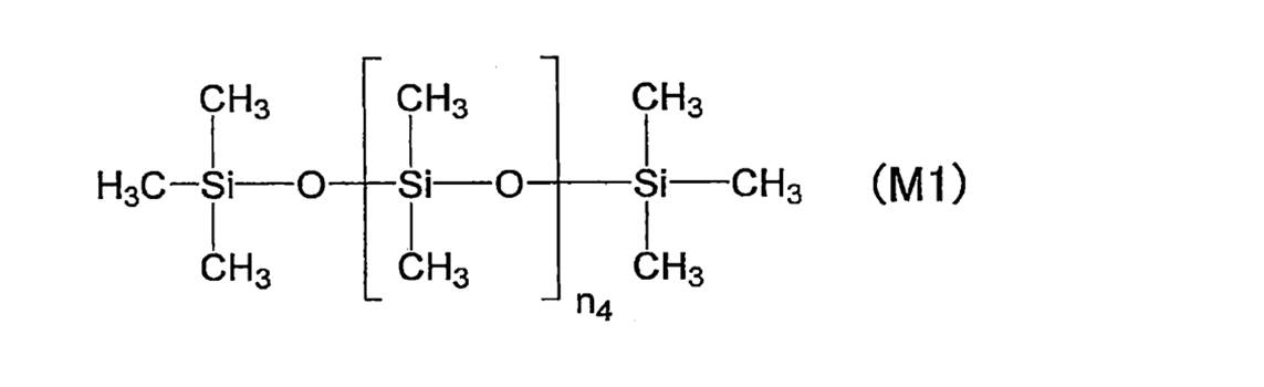
[7] バンプ付き半導体基板と支持基板との間に介在し、かつ前記半導体基板に接する接着層を備える積層体であって、
前記接着層が、[1]~[6]のいずれかに記載の接着剤組成物から形成される層である、積層体。
[8] [7]に記載の積層体における前記半導体基板が加工される工程と、
前記支持基板と加工された前記半導体基板とが離される工程と、
を含む、半導体基板の製造方法。
[9] [7]に記載の積層体を製造する、積層体の製造方法であって、
前記接着層を与える接着剤塗布層が形成される工程と、
前記接着剤塗布層が加熱され、前記接着層が形成される工程と、
を含む、積層体の製造方法。
本発明の接着剤組成物は、半導体基板を加工するために仮接着するための接着層を形成するために好適に使用できる組成物である。
本発明の接着剤組成物は、接着剤成分(S)を含む。
接着剤成分(S)は、ヒドロシリル化反応により硬化するポリオルガノシロキサン成分(A)を含有する。
ポリオルガノシロキサン成分(A)は、下記式(V)で表され、重量平均分子量が60,000以上である重合体(V)を含有する。

また、本発明の接着剤組成物は、接着剤成分(S)と剥離剤成分(B)の他に、例えば、接着剤組成物の粘度等を調整するために、溶媒等のその他の成分を含んでもよい。
本発明の接着剤組成物は、下記実施例でも示すように、バンプの変形を抑制でき、かつ高いエッチングレートを示す接着層を形成することができる。
接着剤成分は、ヒドロシリル化反応により硬化するポリオルガノシロキサン成分(A)を含有する。
本発明のより好ましい一態様においては、ポリオルガノシロキサン成分(A)は、SiO2で表されるシロキサン単位(Q単位)、R1R2R3SiO1/2で表されるシロキサン単位(M単位)、R4R5SiO2/2で表されるシロキサン単位(D単位)及びR6SiO3/2で表されるシロキサン単位(T単位)からなる群より選ばれる1種又は2種以上の単位を含むポリオルガノシロキサン(A1)と、白金族金属系触媒(A2)とを含有する。
また、ポリオルガノシロキサン(A1)は、SiO2で表されるシロキサン単位(Q’単位)、R1’R2’R3’SiO1/2で表されるシロキサン単位(M’単位)、R4’R5’SiO2/2で表されるシロキサン単位(D’単位)及びR6’SiO3/2で表されるシロキサン単位(T’単位)からなる群より選ばれる1種又は2種以上の単位を含むとともに、M’単位、D’単位及びT’単位からなる群より選ばれる少なくとも1種を含むポリオルガノシロキサン(a1)と、SiO2で表されるシロキサン単位(Q”単位)、R1”R2”R3”SiO1/2で表されるシロキサン単位(M”単位)、R4”R5”SiO2/2で表されるシロキサン単位(D”単位)及びR6”SiO3/2で表されるシロキサン単位(T”単位)からなる群より選ばれる1種又は2種以上の単位を含むとともに、M”単位、D”単位及びT”単位からなる群より選ばれる少なくとも1種を含むポリオルガノシロキサン(a2)とを含む。
置換されていてもよい環状アルケニル基の具体例としては、シクロペンテニル、シクロヘキセニル等が挙げられるが、これらに限定されず、その炭素数は、通常4~14であり、好ましくは5~10、より好ましくは5~6である。
本発明の接着剤組成物は、下記式(V)で表され、重量平均分子量が60,000以上である重合体(V)を必須の成分として含有する。
すなわち、本発明の接着剤組成物が含む式(V)で表さる重合体の重量平均分子量は60,000以上である。
本発明の接着剤組成物は、式(V)で表される重合体以外にも、ポリオルガノシロキサン(a1)に包含されるポリオルガノシロキサンを1種又は2種以上を含んでいてもよい。
なお、重合体(V)については、以下で詳しく説明する。

ポリオルガノシロキサン(a1)における、重合体(V)以外のポリオルガノシロキサンの重量平均分子量は、特に限定されないが、それぞれ、通常500~1,000,000であり、本発明の効果を再現性よく実現する観点から、好ましくは5,000~50,000である。
ポリオルガノシロキサン(a2)の重量平均分子量は、特に限定されないが、それぞれ、通常500~1,000,000であり、本発明の効果を再現性よく実現する観点から、好ましくは5,000~50,000である。
なお、本発明において、ポリオルガノシロキサンの重量平均分子量及び数平均分子量並びに分散度は、例えば、GPC装置(東ソー(株)製EcoSEC,HLC-8320GPC)及びGPCカラム(東ソー(株)TSKgel SuperMultiporeHZ-N, TSKgel SuperMultiporeHZ-H)を用い、カラム温度を40℃とし、溶離液(溶出溶媒)としてテトラヒドロフランを用い、流量(流速)を0.35mL/分とし、標準試料としてポリスチレン(昭和電工(株)Shodex)を用いて、測定することができる。
このような白金系の金属触媒は、ポリオルガノシロキサン(a1)のアルケニル基とポリオルガノシロキサン(a2)のSi-H基とのヒドロシリル化反応を促進するための触媒である。
白金とオレフィン類との錯体としては、例えばジビニルテトラメチルジシロキサンと白金との錯体が挙げられるが、これに限定されない。
白金族金属系触媒(A2)の量は、特に限定されないが、通常、ポリオルガノシロキサン(a1)及びポリオルガノシロキサン(a2)の合計量に対して、1.0~50.0ppmの範囲である。
重合抑制剤は、ヒドロシリル化反応の進行を抑制できる限り特に限定されるものではなく、その具体例としては、1-エチニル-1-シクロヘキサノール、1,1-ジフェニル-2-プロピオン-1-オール等のアルキニルアルコール等が挙げられる。
重合抑制剤の量は、特に限定されないが、ポリオルガノシロキサン(a1)及びポリオルガノシロキサン(a2)の合計量に対して、通常、その効果を得る観点から1000.0ppm以上であり、ヒドロシリル化反応の過度な抑制を防止する観点から10000.0ppm以下である。
本発明の接着剤組成物は、ヒドロシリル化反応により硬化するポリオルガノシロキサン成分(A)を構成する前述のポリオルガノシロキサン(a1)として、下記式(V)で表され、重量平均分子量が60,000以上である重合体(V)を含有する。
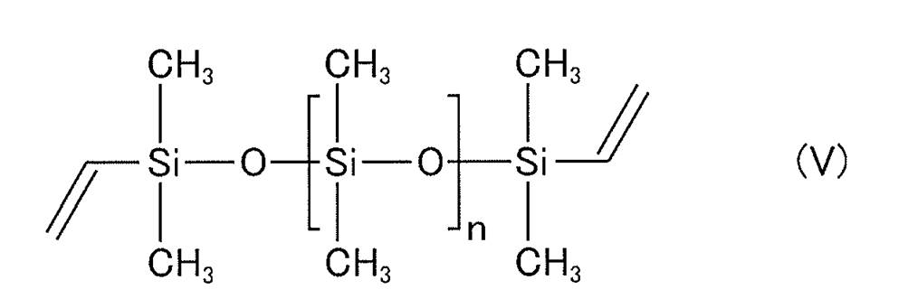
また、合成した式(V)で表される重合体も、その重量平均分子量が所望の値であるときは、そのまま1種単独で用いてもよく、また、重量平均分子量が所望の値になるように、それぞれ別に合成した、重量平均分子量の異なる2種以上の式(V)で表される重合体を組み合わせて用いてもよい。
更に、市販品と合成したものとを組み合わせて用いてもよい。
すわなち、式(V)で表され、重量平均分子量が100,000以上である重合体(V)を含有する接着剤組成物を用いることで、より優れたバンプ変形抑制効果とより高いエッチングレートを示す接着層を再現性よく形成することができる。
なお、良好なバンプ変形抑制効果と高いエッチングレートの両方をよりバランスよく発揮させるという観点からは、重合体(V)の重量平均分子量は、好ましくは160,000以下であり、より好ましくは150,000以下であり、より一層好ましくは130,000以下であり、更に好ましくは110,000以下である。
また、重量平均分子量(Mw)と数平均分子量(Mn)から求められる重合体(V)の分子量分布(Mw/Mn)は、良好なバンプ変形抑制効果と高いエッチングレートの両方をよりバランスよく発揮させるという観点から、好ましくは3.2~25であり、より好ましくは3.2~15であり、より一層好ましくは9~13である。
例えば、重合体(V)を得る方法として、以下の方法を挙げることができる。
(i)上記式(V)で表され、重量平均分子量が15,000~20,000である重合体(V2)と、上記式(V)で表され、重量平均分子量が100,000~200,000である重合体(V1)とを原料として混合して用いることで、上記式(V)で表され、重量平均分子量が60,000以上である重合体(V)を得ることができる。
重合体(V)を得る方法のより好ましい態様として、以下の方法を挙げることができる。
(i-a)上記(i)の方法において、重合体(V2)と重合体(V1)との混合割合を、質量比で、重合体(V2):重合体(V1)=0.04~1.1:1とする。
(i-b)上記(i)の方法において、重合体(V2)と重合体(V1)との混合割合を、質量比で、重合体(V2):重合体(V1)=0.04~0.5:1とする。
(i-c)上記(i)の方法において、重合体(V2)と重合体(V1)との混合割合を、質量比で、重合体(V2):重合体(V1)=0.3~0.5:1とする。
上記(i-b)の方法によれば、重量平均分子量が100,000以上である重合体(V)を再現性よく得ることができる。上記(i-b)の方法で得られる重合体(V)を用いると、(i-a)の方法で得られる重合体(V)を用いた場合より、より優れたバンプ変形抑制効果を示す接着層を再現性よく形成することができる。
また、上記(i-c)の方法によれば、重量平均分子量が100,000~130,000である重合体(V)を再現性よく得ることができる。上記(i-c)の方法で得られる重合体(V)を用いると、(i-a)の方法で得られる重合体(V)を用いた場合より、より優れたバンプ変形抑制効果とより高いエッチングレートを示す接着層を再現性よく形成することができる。
(ii)上記式(V)で表され、重量平均分子量が16,000程度の重合体(V2-1)と、上記式(V)で表され、重量平均分子量が150,000程度の重合体(V1-1)とを原料として混合して用いることで、重量平均分子量が60,000以上である重合体(V)を得ることができる。
重合体(V)を得る方法のより好ましい態様として、以下の方法を挙げることができる。
(ii-a)上記(ii)の方法において、重合体(V2-1)と重合体(V1-1)との混合割合を、質量比で、重合体(V2-1):重合体(V1-1)=0.04~1.1:1とする。
(ii-b)上記(ii)の方法において、重合体(V2)と重合体(V1-1)との混合割合を、質量比で、重合体(V2-1):重合体(V1-1)=0.04~0.5:1とする。
(ii-c)上記(ii)の方法において、重合体(V2)と重合体(V1-1)との混合割合を、質量比で、重合体(V2-1):重合体(V1-1)=0.3~0.5:1とする。
上記(ii-b)の方法によれば、重量平均分子量が100,000以上である重合体(V)をより再現性よく得ることができる。上記(ii-b)の方法で得られる重合体(V)を用いると、(ii-a)の方法で得られる重合体(V)を用いた場合より、より優れたバンプ変形抑制効果を示す接着層をより再現性よく形成することができる。
また、上記(ii-c)の方法によれば、重量平均分子量が100,000~130,000である重合体(V)をより再現性よく得ることができる。上記(ii-c)の方法で得られる重合体(V)を用いると、(ii-a)の方法で得られる重合体(V)を用いた場合より、より優れたバンプ変形抑制効果とより高いエッチングレートを示す接着層をより再現性よく形成することができる。
なお、所望の重量平均分子量を得るための混合比率は、当業者であれば過度の試行錯誤なく、用いる各重合体の重量平均分子量を考慮して適宜決定することができる。
すなわち、接着剤組成物の調製に当たり、重合体(V)は、その調製前に個別のものとして準備されている必要はなく、接着剤組成物が調製される過程で、所望の重量平均分子量を有さない式(V)で表される重合体2種以上が混合されて、最終的に接着剤組成物中で重合体(V)が実現されてもよい。
更に、重合体(V)である重合体(V-1)の重合平均分子量を調整するために、重合体(V-1)を、異なる重量平均分子量を有する、1種又は2種以上の式(V)で表される重合体を混合し、重合体(V)である重合体(V-2)としてもよい。
そして、式(V)で表される重合体でも、特に重量平均分子量が60,000以上という分子量の大きい重合体を含有させることで、本発明の目的を達成することができる。重合体(V)のような重量平均分子量の高い重合体がヒドロシリル化反応によって架橋することで、外部からの加熱加圧時においてバンプの保護性能を高めることができるとともに、洗浄時には洗浄剤組成物が膜中に浸透しやすくなる効果を示すことにつながっているからと推察される。
本発明の接着剤組成物は、前述の接着剤成分(S)の他に、ポリオルガノシロキサンを含む剥離剤成分(B)(以下、成分(B)ともいう)を含有してもよい。
好ましい態様としては、本発明の接着剤組成物は、接着剤成分(S)として、硬化する成分であるポリオルガノシロキサン成分(A)(以下、成分(A)ともいう)とともに、剥離剤成分となる硬化反応を起こさない成分(B)を含む。
ここで、「硬化反応を起こさない」とは、あらゆる硬化反応を起こさないことを意味するのではなく、硬化する成分(A)に生じる硬化反応を起こさないことを意味する。
成分(B)を接着剤組成物に含めることで、得られる接着層を再現性よく好適に剥離することができるようになる。
このような剥離剤成分(B)として、典型的には、ポリオルガノシロキサンが挙げられ、その具体例としては、エポキシ基含有ポリオルガノシロキサン、メチル基含有ポリオルガノシロキサン、フェニル基含有ポリオルガノシロキサン等が挙げられるが、これらに限定されない。
また、剥離剤成分(B)としては、ポリジメチルシロキサンが挙げられる。当該ポリジメチルシロキサンは変性されていてもよい。変性されていてもよいポリジメチルシロキサンとしては、例えば、エポキシ基含有ポリジメチルシロキサン、無変性のポリジメチルシロキサン、フェニル基含有ポリジメチルシロキサン等が挙げられるが、これらに限定されない。
エポキシ基を含む有機基におけるエポキシ基は、その他の環と縮合せずに、独立したエポキシ基であってもよく、1,2-エポキシシクロヘキシル基のように、その他の環と縮合環を形成しているエポキシ基であってもよい。
エポキシ基を含む有機基の具体例としては、3-グリシドキシプロピル、2-(3,4-エポキシシクロヘキシル)エチルが挙げられるが、これらに限定されない。
本発明において、エポキシ基含有ポリオルガノシロキサンの好ましい一例としては、エポキシ基含有ポリジメチルシロキサンを挙げることができるが、これに限定されない。
本発明の好ましい態様においては、エポキシ基含有ポリオルガノシロキサンの具体例としては、D10単位のみからなるポリオルガノシロキサン、D10単位とQ単位とを含むポリオルガノシロキサン、D10単位とM単位とを含むポリオルガノシロキサン、D10単位とT単位とを含むポリオルガノシロキサン、D10単位とQ単位とM単位とを含むポリオルガノシロキサン、D10単位とM単位とT単位とを含むポリオルガノシロキサン、D10単位とQ単位とM単位とT単位とを含むポリオルガノシロキサン等が挙げられる。
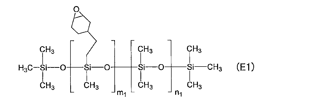
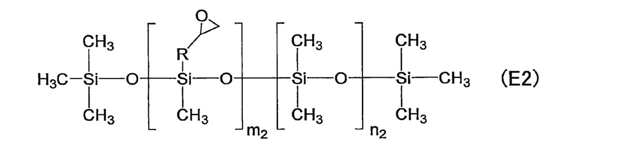

R21は、ケイ素原子に結合する基であり、アルキル基を表し、アルキル基の具体例としては、前述の例示を挙げることができる。中でも、R21としては、メチル基が好ましい。
本発明において、メチル基含有ポリオルガノシロキサンの好ましい一例としては、ポリジメチルシロキサンを挙げることができるが、これに限定されない。
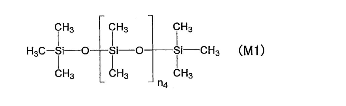
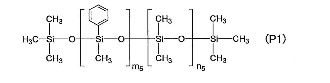
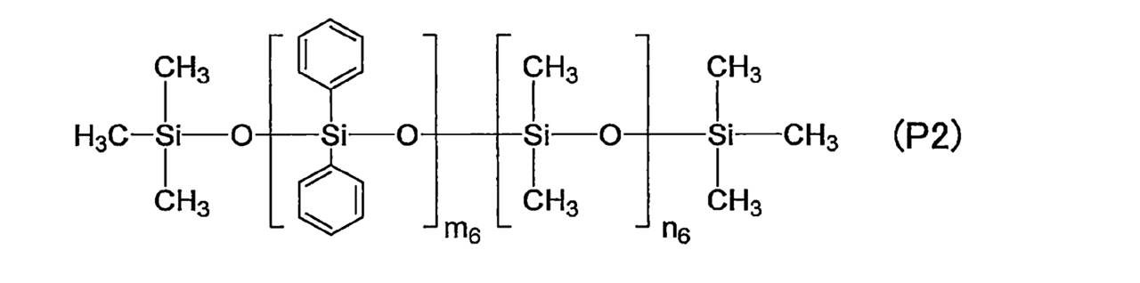
ポリオルガノシロキサンの市販品としては、例えば、ワッカーケミ社製の製品であるWACKERSILICONE FLUID AK シリーズ(AK50、AK 350、AK 1000、AK 10000、AK 1000000)やGENIOPLAST GUM、信越化学工業(株)製 ジメチルシリコーンオイル(KF-96L、KF-96A、KF-96、KF-96H、KF-69、KF-965、KF-968)、環状ジメチルシリコーンオイル(KF-995);ゲレスト社製 エポキシ基含有ポリオルガノシロキサン(商品名CMS-227、ECMS-327)、信越化学工業(株)製 エポキシ基含有ポリオルガノシロキサン(KF-101、KF-1001、KF-1005、X-22-343)、ダウコーニング社製 エポキシ基含有ポリオルガノシロキサン(BY16-839);ゲレスト社製 フェニル基含有ポリオルガノシロキサン(PMM-1043、PMM-1025、PDM-0421、PDM-0821)、信越化学工業(株)製 フェニル基含有ポリオルガノシロキサン(KF50-3000CS)、MOMENTIVE社製 フェニル基含有ポリオルガノシロキサン(TSF431、TSF433)等が挙げられるが、これらに限定されない。
ここで、本発明において、特に剥離剤成分(H)であるポリオルガノシロキサンの複素粘度については、25℃でレオメータを用いて測定した値を意味する。このような複素粘度は、例えば、アントンパール(株)製 レオメータMCR-302を用いて測定することができる。
本発明の接着剤組成物は、剥離剤成分(B)として、剥離剤成分(H)を含有する接着剤組成物が好ましいが、該剥離剤成分(H)以外にも、剥離剤成分(B)に包含される剥離剤成分を1種又は2種以上含有させることができる。
本発明の接着剤組成物は、粘度の調整等を目的に、溶媒を含んでいてもよく、溶媒の具体例としては、脂肪族炭化水素、芳香族炭化水素、ケトン等が挙げられるが、これらに限定されない。
本発明において、膜構成成分とは、組成物に含まれる溶媒以外の成分を意味する。
接着剤組成物の製造方法の好ましい態様として、例えば、本発明の接着剤組成物は、接着剤成分(S)と、剥離剤成分(B)と、用いる場合には溶媒とを混合することで製造できる。
その混合順序は特に限定されるものではないが、容易にかつ再現性よく本発明の接着剤組成物を製造できる方法の一例としては、例えば、接着剤成分(S)と剥離剤成分(B)を溶媒に溶解させる方法や、接着剤成分(S)と剥離剤成分(B)の一部を溶媒に溶解させ、残りを溶媒に溶解させ、得られた溶液を混合する方法が挙げられるが、これらに限定されない。なお、接着剤組成物を調製する際、成分が分解したり変質したりしない範囲で、適宜加熱してもよい。
本発明においては、異物を除去する目的で、接着剤組成物を製造する途中で又は全ての成分を混合した後に、フィルター等を用いてろ過してもよい。
本発明の積層体は、バンプ付き半導体基板と支持基板と接着層とを備える。
接着層は、バンプ付き半導体基板と支持基板との間に介在し、かつ半導体基板に接する。
接着層は、上述した本発明の接着剤組成物から形成される層である。
積層体は、半導体基板を加工するため仮接着するために使用され、積層体における半導体基板の加工後に支持基板と半導体基板とが離される用途に好適に使用できる。
本発明の積層体において、接着層の層数には特に制限はなく、目的に応じて適宜選択される。例えば、積層体において、接着層は1層であっても、2層以上であってもよい。
また、本発明の積層体は、半導体基板と支持基板の間に接着層以外の層を含んでもよく、例えば、半導体基板と支持基板の間に接着層と剥離層とを含む積層体が挙げられる。
本発明の積層体の好ましい一態様として、半導体基板、接着層、剥離層、支持基板をこの順で有する積層体が挙げられる。
したがって、本発明の積層体は、バンプ変形の抑制効果と、高いエッチングレートのいずれをも満足できる接着層を有する積層体となる。
図1Aは積層体の一例の概略断面図である。
図1Aの積層体は、バンプ1aを有する半導体基板1と、接着層2と、支持基板4とをこの順で有する。
半導体基板1が有するバンプ1aは、支持基板4側に配されている。
接着層2は、半導体基板1と支持基板4との間に介在する。接着層2は、半導体基板1に接する。そして、接着層2は、バンプ1aを覆っている。
図1Bは積層体の他の一例の概略断面図である。
図1Bの積層体は、バンプ1aを有する半導体基板1と、接着層2と、剥離層3と、支持基板4とをこの順で有する。
半導体基板1が有するバンプ1aは、支持基板4側に配されている。
接着層2は、半導体基板1と支持基板4との間に介在する。接着層2は、半導体基板1に接する。そして、接着層2は、バンプ1aを覆っている。
剥離層3は、接着層2と支持基板4との間に介在する。剥離層3は、接着層2及び支持基板4に接している。
本発明の積層体の各構成について、以下詳しく説明する。
半導体基板は、バンプを有する。バンプとは、突起状の端子である。
積層体において、半導体基板は、支持基板側にバンプを有する。
半導体基板において、バンプは、通常、回路が形成された面上に形成されている。回路は、単層であってもよし、多層であってもよい。回路の形状としては特に制限されない。
半導体基板において、バンプを有する面と反対側の面(裏面)は、加工に供される面である。
半導体基板の形状は、特に限定されないが、例えば、円盤状である。なお、円盤状の半導体基板は、その面の形状が完全な円形である必要はなく、例えば、半導体基板の外周は、オリエンテーション・フラットと呼ばれる直線部を有していてもよいし、ノッチと呼ばれる切込みを有していてもよい。
円盤状の半導体基板の厚さは、半導体基板の使用目的などに応じて適宜定めればよく、特に限定されないが、例えば、500~1,000μmである。
円盤状の半導体基板の直径としては、半導体基板の使用目的などに応じて適宜定めればよく、特に限定されないが、例えば、100~1,000mmが挙げられる。
バンプとしては、例えば、ボールバンプ、印刷バンプ、スタッドバンプ、めっきバンプなどが挙げられる。
通常、バンプ高さ1~200μm程度、バンプ直径1~200μm、バンプピッチ1~500μmという条件からバンプの高さ、直径及びピッチは適宜決定される。
バンプの材質としては、例えば、低融点はんだ、高融点はんだ、スズ、インジウム、金、銀、銅などが挙げられる。バンプは、単一の成分のみで構成されていてもよいし、複数の成分から構成されていてもよい。より具体的には、SnAgバンプ、SnBiバンプ、Snバンプ、AuSnバンプ等のSnを主体とした合金めっき等が挙げられる。
また、バンプは、これらの成分の少なくともいずれかからなる金属層を含む積層構造を有してもよい。
支持基板としては、半導体基板が加工される際に、半導体基板を支持できる部材であれば、特に限定されないが、例えば、ガラス製支持基板、シリコン製支持基板などが挙げられる。
円盤状の支持基板の厚さは、半導体基板の大きさなどに応じて適宜定めればよく、特に限定されないが、例えば、500~1,000μmである。
円盤状の支持基板の直径は、半導体基板の大きさなどに応じて適宜定めればよく、特に限定されないが、例えば、100~1,000mmである。
接着層は、支持基板と半導体基板との間に介在する。
接着層は、半導体基板と接する。
接着層の厚さは、特に限定されるものではないが、良好なバンプ変形抑制効果を得るための観点から、好ましくは20~120μmであり、より好ましくは40~100μmである。
接着剤組成物から接着層を形成する方法については、以下で記載する<積層体の製造方法>の説明箇所で詳しく述べる。
本発明の積層体は、剥離層を備えていてもよい。
積層体が剥離層を有する場合、例えば、剥離層は、支持基板及び接着層に接するように配することができる。
剥離剤組成物は、更に、架橋剤、酸触媒、界面活性剤を含むことができる。
本発明の積層体が備える剥離層に光を照射して剥離をする場合、波長190nm~600nmの光を吸収し変質するノボラック樹脂が好ましく、波長が308nm、343nm、355nm又は365nmのレーザー等の光の照射によって変質するノボラック樹脂がより好ましい。

剥離剤組成物に含有させるノボラック樹脂、及びノボラック樹脂を用いた剥離層については、国際公開第2019/088103号に記載のノボラック樹脂及び該ノボラック樹脂を用いた剥離層を参酌することができる。
本発明に係る積層体が備える剥離層の厚さは、剥離剤成分の種類や所望の剥離性の程度等を考慮して適宜設定されるものではあるが、通常5~10,000nmであり、薄膜による剥離能の悪化を抑制し、剥離性に優れる剥離層を再現性よく得る観点等から、好ましくは10nnm以上、より好ましくは50nm以上、より一層好ましくは100nm以上であり、厚膜による不均一性を回避する観点等から、好ましくは5,000nm以下、より好ましくは1,000nm以下、より一層好ましくは500nm以下である。
積層体における接着層が、本発明の接着剤組成物を用いて形成される接着層のみかつ単層からなる場合には、本発明の積層体の製造方法は、接着層を形成する工程(接着剤塗布層形成工程及び接着層形成工程)を含み、更に必要に応じて、貼り合せ工程などのその他の工程を含む。この場合における積層体の製造方法については、下記<<第一の実施態様>>の欄で詳しく説明する。
また、積層体が、接着層と剥離層とを含む場合には、本発明の積層体の製造方法は、接着層を形成する工程(接着剤塗布層形成工程及び接着層形成工程)の他、剥離層を形成する工程を含み、更に必要に応じて、貼り合せ工程などのその他の工程を含む。この場合における積層体の製造方法については、下記<<第二の実施態様>>の欄で詳しく説明する。
接着剤塗布層形成工程及び接着層形成工程を経ることにより接着層を形成する。
接着剤塗布層形成工程では、例えば、接着剤組成物をバンプ付き半導体基板に塗布して、接着剤塗布層を形成する。
塗布方法は、特に限定されるものではないが、通常、スピンコート法である。なお、別途スピンコート法等で塗布膜を形成し、シート状の塗布膜を、接着剤塗布層として貼付する方法を採用し得る。
接着剤塗布層の厚さは、積層体中の接着層の厚さ等を考慮して、適宜決定される。
接着剤組成物が溶媒を含む等の理由により、塗布した接着剤組成物の塗膜を乾燥させる目的で、塗布した接着剤組成物を加熱してもよい(前加熱処理)。
塗布した接着剤組成物の加熱温度は、接着剤組成物が含む接着剤成分の種類や量、溶媒が含まれるか否か、用いる溶媒の沸点、所望の接着層の厚さ等に応じて異なるため一概に規定できないが、通常80~150℃、その加熱時間は、通常30秒~5分である。
加熱は、ホットプレート、オーブン等を用いて行うことができる。
接着層形成工程は、接着剤塗布層を加熱し、接着剤組成物を硬化させて接着層を形成する。
接着層形成工程としては、支持基板と接着剤塗布層が接しかつ接着剤塗布層と半導体基板が接した状態で、接着剤塗布層が加熱され、接着層が形成される工程であれば、特に限定されない。
例えば、接着剤塗布層が形成された半導体基板と支持基板とを用いて、接着剤塗布層を挟み込むように2つの基板(半導体基板及び支持基板)を配することによって、支持基板と接着剤塗布層が接するようにし、かつ接着剤塗布層と半導体基板が接するようにした後、加熱処理を施せばよい(後加熱処理)。
加熱の温度及び時間としては、接着剤塗布層が接着層に転化される温度及び時間であれば、特に限定されない。
加熱の温度としては、十分な硬化速度を実現する観点等から、好ましくは120℃以上、より好ましくは150℃以上であり、積層体を構成する各層(支持基板及び半導体基板を含む)の変質を防ぐ観点等から、好ましくは250℃以下である。さらに好ましくは、180~200℃である。
加熱の時間としては、積層体を構成する各層(支持基板及び半導体基板を含む)の好適な接合を実現する観点から、好ましくは1分以上であり、より好ましくは5分以上であり、過度の加熱による各層への悪影響等を抑制又は回避する観点から、好ましくは180分以下であり、より好ましくは120分以下である。さらに好ましくは、基板処理効率の観点から1~20分である。
加熱は、ホットプレート、オーブン等を用いて行うことができる。
接着剤塗布層形成工程と接着層形成工程との間には、半導体基板と支持基板との貼り合せを十分なものとするために、貼り合せ工程を行うことが好ましい。
貼り合せ工程としては、基板と層の貼り合わせができ、かつ基板や層に損傷を与えない限り特に限定されるものではないが、典型的には、支持基板及び半導体基板の厚さ方向に荷重が掛け得られる工程であり、より好ましくは、減圧下で支持基板及び半導体基板の厚さ方向に荷重が掛け得られる工程である。
荷重は、基板と層の貼り合わせができ、かつ基板や層に損傷を与えない限り特に限定されるものではないが、例えば、10~1,000Nである。
減圧度は、基板と層の貼り合わせができ、かつ基板や層に損傷を与えない限り特に限定されるものではないが、例えば、10~10,000Paである。
剥離層を含む積層体の製造方法の好ましい一態様として、前述のノボラック樹脂等の有機樹脂を含む剥離剤組成物からなる剥離層を用いた場合を例に、以下、積層体の製造方法を説明する。
加熱の温度及び時間としては、接着剤塗布層が接着層に転化される温度及び時間であれば、特に限定されない。
加熱条件としては、前述の<<第一の実施態様>>の接着層形成工程で記載したと同様の条件を用いることができる。
接着剤塗布層形成工程と接着層形成工程との間には、半導体基板と支持基板との貼り合せを十分なものとするために、貼り合せ工程を行うことが好ましい。
貼り合わせ工程としては、前述の<<第一の実施態様>>で記載したと同様の条件を用いることができる。
本発明の積層体は、半導体基板を加工するため仮接着するために使用され、積層体における半導体基板の加工後に支持基板と半導体基板とが離される用途に好適に使用できる。
本発明の半導体基板の製造方法は、半導体基板が加工される加工工程と、支持基板と加工された半導体基板とが離される剥離工程とを少なくとも含み、更に必要に応じて、除去工程等のその他の工程を含む。
加工工程としては、本発明に係る積層体における半導体基板が加工される工程であれば、特に限定されないが、例えば、研磨処理、貫通電極形成処理などを含む。
例えば、各種加工工程において、高温高圧下で加工処理される場合があるが、本発明の積層体は、高温(例えば、250~350℃)や高圧下で処理されても、半導体基板のバンプ変形を有効に防止することができる。
研磨処理としては、例えば、半導体基板のバンプが存在する面と反対側の面を研磨し、半導体基板を薄くする処理であれば、特に限定されないが、例えば、研磨剤や砥石を用いた物理的研磨などが挙げられる。
研磨処理は、半導体基板の研磨に使用されている一般的な研磨装置を用いて行うことができる。
研磨処理によって、半導体基板の厚さが減り、所望の厚さに薄化した半導体基板が得られる。薄化した半導体基板の厚みとしては、特に限定されないが、例えば、30~300μmであってもよいし、30~100μmであってもよい。
研磨された半導体基板には、複数の薄化された半導体基板を積層した際に薄化された半導体基板間の導通を実現するための貫通電極が形成される場合がある。
そのため、半導体基板の製造方法は、研磨処理の後であって剥離工程の前に、研磨された半導体基板に貫通電極が形成される貫通電極形成処理を含んでいてもよい。
半導体基板に貫通電極を形成する方法としては、特に限定されないが、例えば、貫通孔を形成し、形成された貫通孔に導電性材料を充填することなどが挙げられる。
貫通孔の形成は、例えば、フォトリソグラフィーによって行われる。
貫通孔への導電性材料の充填は、例えば、めっき技術によって行われる。
剥離工程は、加工工程の後に、支持基板と加工された半導体基板とが離される工程である限り特に限定されない。
例えば、溶剤剥離、光照射による剥離(レーザー光、非レーザー光)、鋭部を有する機材(いわゆるディボンダー)による機械的な剥離、支持体とウエハーとの間でマニュアルで引きはがす剥離等が挙げられるが、これらに限定されない。通常、剥離は、本発明の積層体を製造し、それに所定の加工等が行われた後に、実施される。
特に、積層体が剥離層を含む場合であって、剥離層が上述したように光を吸収して剥離能向上に必要な変質が生じる有機樹脂を用いて形成された剥離層である場合には、例えば、支持体側からレーザーを照射することにより剥離層を剥がすことができる。
レーザー光の波長は190nm~400nm、又は190nm~600nmの波長(例えば、308nm、355nm、532nm)の紫外光を用いて行われる。
剥離は、パルスレーザーの加工エネルギー密度を50~500mJ/cm2程度とすることで行うことができる。
積層体が剥離層を含む場合、通常、通常、剥離層内部又は剥離層と隣接する基板若しくは層(例えば接着層)との界面で剥離が起こる。剥離層内部で剥離が起こるとは、剥離層が開裂することを意味する。
<<除去工程>>
除去工程としては、剥離工程の後に、接着層が除去される工程であれば、特に限定されないが、例えば、洗浄剤組成物を用いて接着層を溶解除去する方法が挙げられる。また、溶解除去に除去テープ等を用いた除去を組み合わせてもよい。
洗浄剤組成物を用いる場合、例えば、接着層付き半導体基板を洗浄剤組成物に浸漬したり、洗浄剤組成物を吹き付けたりすることができる。
本発明の接着剤組成物を形成してなる接着剤は、下記実施例で示すように高いエッチングレートを示すため、本発明の積層体は、剥離工程後における半導体基板上に残された接着層の溶解除去を容易に行うことができる。
第四級アンモニウム塩は、第四級アンモニウムカチオンと、アニオンとから構成されるものであって、この種の用途に用いられるものであれば特に限定されるものではない。
このような第四級アンモニウムカチオンとしては、典型的には、テトラ(炭化水素)アンモニウムカチオンが挙げられる。一方、それと対を成すアニオンとしては、水酸化物イオン(OH-);フッ素イオン(F-)、塩素イオン(Cl-)、臭素イオン(Br-)、ヨウ素イオン(I-)等のハロゲンイオン;テトラフルオロホウ酸イオン(BF4 -);ヘキサフルオロリン酸イオン(PF6 -)等が挙げられるが、これらに限定されない。
第四級アンモニウム塩中、ハロゲン原子は、カチオンに含まれていても、アニオンに含まれていてもよいが、好ましくはアニオンに含まれる。
フッ化テトラ(炭化水素)アンモニウムにおける炭化水素基の具体例としては、炭素数1~20のアルキル基、炭素数2~20のアルケニル基、炭素数2~20のアルキニル基、炭素数6~20のアリール基等が挙げられる。
より好ましい一態様においては、フッ化テトラ(炭化水素)アンモニウムは、フッ化テトラアルキルアンモニウムを含む。
フッ化テトラアルキルアンモニウムの具体例としては、フッ化テトラメチルアンモニウム、フッ化テトラエチルアンモニウム、フッ化テトラプロピルアンモニウム、フッ化テトラブチルアンモニウム(テトラブチルアンモニウムフルオリドともいう)等が挙げられるが、これらに限定されない。中でも、フッ化テトラブチルアンモニウムが好ましい。
図2A~図2Fは、積層体の製造及び薄化ウエハーの製造を行う一態様を説明するための図である。
まず、バンプ1aを有するウエハー1を用意する(図2A)。
次に、ウエハー1のバンプ1aが存在する面上に、塗布装置12を用いたスピンコーティングによって接着剤組成物を塗布し、接着剤塗布層2aを形成する(図2B)。
次に、支持基板4上に塗布装置(不図示)を用いたスピンコーティングによって剥離剤組成物を塗布し、剥離剤組成物を加熱することにより硬化させ剥離層3を形成し、剥離層3が形成された支持基板4を用意する(図2C)。
次に、接着剤塗布層2aが形成されたウエハー1と、剥離層3が形成された支持基板4とを、接着剤塗布層2aと剥離層3とを挟み込むようにして、減圧下でウエハー1と支持基板4とを貼り合わせた後、ウエハー1のバンプ1aが存在する面と反対側の面に、加熱装置(ホットプレート)13を配し、加熱装置13によって接着剤塗布層2aを加熱して接着剤組成物を硬化させ接着層2に転化させる(図2D)。
図2A~図2Dで示した工程によって、積層体が得られる。
次に、薄化ウエハーの製造の一例を説明する。
次に、研磨装置(不図示)を用いてウエハー1のバンプ1aが存在する面と反対側の面を研磨し、ウエハー1を薄化する(図2E)。なお、薄化されたウエハー1に対して貫通電極の形成などが施されてもよい。
次に、支持基板4側から光(紫外光)を照射(不図示)することにより、薄化したウエハー1と支持基板4とを剥離する(図2F)。この際、接着層2と剥離層3とが剥離することによって、薄化したウエハー1と支持基板4とが剥離する。
次に、洗浄装置(不図示)を用いて、洗浄剤組成物によって薄化したウエハー1上から接着層2を溶解除去することによって、薄化したウエハー1を洗浄する。
以上によって薄化したウエハー1が得られる。
(1)撹拌機A:(株)シンキー製 自転公転ミキサー ARE-500
(2)粘度計:東機産業(株)製 回転粘度計TVE-22H
(3)複素粘度計:アントンパール(株)製 レオメータMCR-302
(4)撹拌機H:アズワン製 加温型ロッキングミキサー HRM-1
(5)接触式膜厚計:(株)東京精密製 ウエハー厚さ測定装置 WT-425
(6)光学式膜厚計(膜厚測定):フィルメトリクス(株)製 F-50
(7)真空貼り合わせ装置:ズースマイクロテック(株)製、オートボンダー
(8)高剛性研削盤:(株)東京精密製 HRG300
(9)ダイシングマシン:(株)東京精密製 SS30
(10)加熱圧着装置:アユミ工業(株)製、張り付け装置
ポリオルガノシロキサンの重量平均分子量及び数平均分子量並びに分散度は、GPC装置(東ソー(株)製EcoSEC HLC―8320GPC)及びGPCカラム(東ソー(株)TSKgel SuperMultiporeHZ-N、TSKgel SuperMultiporeHZ-H)を用い、カラム温度を40℃とし、溶離液(溶出溶媒)としてテトラヒドロフランを用い、流量(流速)を0.35mL/分とし、標準試料としてポリスチレン(昭和電工(株)Shodex)を用いて、測定した。
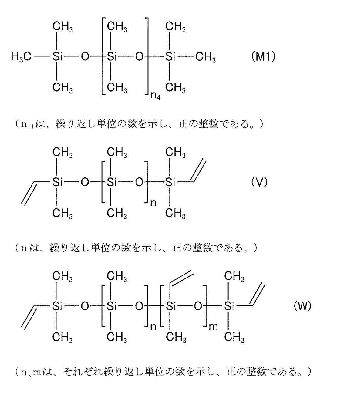
[調製例1-1]
自転公転ミキサー専用300mL撹拌容器に、前述の成分(a1)としてビニル基含有MQ樹脂(ワッカーケミ社製)のp-メンタン溶液(濃度80.6質量%)62.05g、前述の成分(A3)として1,1-ジフェニル-2-プロピン-1-オール(東京化成工業(株)製)0.25gを加え、撹拌機Aによる5分間の撹拌を行ない、混合物(I)を得た。
得られた混合物(I)に、前述の成分(B)として上記式(M1)で表されるポリオルガノシロキサン(複素粘度6000Pa・s、重量平均分子量642,000(分散度2.6)、ワッカーケミ社製 商品名GENIOPLASTGUM)10.09g、前述の成分(a1)として上記式(V)で表される粘度100000mPa・sのビニル基含有直鎖状ポリジメチルシロキサン(ワッカーケミ社製)(以下、ビニル基含有直鎖状ポリジメチルシロキサンv1ともいう)30.17g、前述の成分(a2)として粘度100mPa・sのSiH基含有直鎖状ポリジメチルシロキサン(ワッカーケミ社製)8.33g、溶媒としてp-メンタン(日本テルペン化学(株)製)24.56gを加え、更にそこへ、前述の成分(A3)として1-エチニル-1-シクロヘキサノール(ワッカーケミ社製)0.26gを加え、撹拌機Aで10分間撹拌し、混合物(II)を得た。
前述の成分(A2)として白金触媒(ワッカーケミ社製)0.10gと、前述の成分(a1)として上記式(V)で表される粘度200mPa・sのビニル基含有直鎖状ポリジメチルシロキサン(ワッカーケミ社製)(以下、ビニル基含有直鎖状ポリジメチルシロキサンv2ともいう)28.96gとを撹拌機Aで5分間撹拌し、混合物(III)を得た。
得られた混合物(III)のうち11.76gを混合物(II)に加え、撹拌機Aで5分間撹拌し、混合物(IV)を得た。
最後に、得られた混合物(IV)をナイロンフィルター300メッシュでろ過し、接着剤組成物を得た。なお、回転粘度計を用いて測定した接着剤組成物の粘度は、3600mPa・sであった。
接着剤組成物に含有される上記式(V)で表される重合体の重量平均分子量は、109,381であり、Mw/Mnは11.5であった。
自転公転ミキサー専用150mL撹拌容器に、前述の成分(a1)としてビニル基含有MQ樹脂(ワッカーケミ社製)のp-メンタン溶液(濃度85.1質量%)35.30g、前述の成分(A3)として1,1-ジフェニル-2-プロピン-1-オール(東京化成工業(株)製)0.15gを加え、撹拌機Aによる5分間の撹拌を行ない、混合物(I)を得た。
得られた混合物(I)に、前述の成分(B)として上記式(M1)で表されるポリオルガノシロキサン(複素粘度6000Pa・s、重量平均分子量642,000(分散度2.6)、ワッカーケミ社製 商品名GENIOPLASTGUM)のp-メンタン溶液(濃度60.3質量%)10.01g、前述の成分(a1)として上記式(V)で表される粘度100000mPa・sのビニル基含有直鎖状ポリジメチルシロキサン(ワッカーケミ社製)24.08g、前述の成分(a2)として粘度100mPa・sのSiH基含有直鎖状ポリジメチルシロキサン(ワッカーケミ社製)5.00g、溶媒としてp-メンタン(日本テルペン化学(株)製)13.02gを加え、更にそこへ、前述の成分(A3)として1-エチニル-1-シクロヘキサノール(ワッカーケミ社製)0.15gを加え、撹拌機Aで10分間撹拌し、混合物(II)を得た。
前述の成分(A2)として白金触媒(ワッカーケミ社製)0.03gと、前述の成分(a1)として上記式(V)で表される粘度200mPa・sのビニル基含有直鎖状ポリジメチルシロキサン(ワッカーケミ社製)1.53gとを撹拌機Aで5分間撹拌し、混合物(III)を得た。
得られた混合物(III)のうち1.04gを混合物(II)に加え、撹拌機Aで5分間撹拌し、混合物(IV)を得た。
最後に、得られた混合物(IV)をナイロンフィルター300メッシュでろ過し、接着剤組成物を得た。なお、回転粘度計を用いて測定した接着剤組成物の粘度は、5200mPa・sであった。
接着剤組成物に含有される上記式(V)で表される重合体の重量平均分子量は、130,814であり、Mw/Mnは3.27であった。
自転公転ミキサー専用150mL撹拌容器に、前述の成分(a1)としてビニル基含有MQ樹脂(ワッカーケミ社製)のp-メンタン溶液(濃度85.1質量%)35.31g、前述の成分(A3)として1,1-ジフェニル-2-プロピン-1-オール(東京化成工業(株)製)0.15gを加え、撹拌機Aによる5分間の撹拌を行ない、混合物(I)を得た。
得られた混合物(I)に、前述の成分(B)として上記式(M1)で表されるポリオルガノシロキサン(複素粘度6000Pa・s、重量平均分子量642,000(分散度2.6)、ワッカーケミ社製 商品名GENIOPLASTGUM)のp-メンタン溶液(濃度60.3質量%)10.02g、前述の成分(a1)として上記式(V)で表される粘度100000mPa・sのビニル基含有直鎖状ポリジメチルシロキサン(ワッカーケミ社製)12.02g、前述の成分(a2)として粘度100mPa・sのSiH基含有直鎖状ポリジメチルシロキサン(ワッカーケミ社製)5.00g、溶媒としてp-メンタン(日本テルペン化学(株)製)13.00gを加え、更にそこへ、前述の成分(A3)として1-エチニル-1-シクロヘキサノール(ワッカーケミ社製)0.15gを加え、撹拌機Aで10分間撹拌し、混合物(II)を得た。
前述の成分(A2)として白金触媒(ワッカーケミ社製)0.03gと、前述の成分(a1)として上記式(V)で表される粘度200mPa・sのビニル基含有直鎖状ポリジメチルシロキサン(ワッカーケミ社製)19.54gとを撹拌機Aで5分間撹拌し、混合物(III)を得た。
得られた混合物(III)のうち13.04gを混合物(II)に加え、撹拌機Aで5分間撹拌し、混合物(IV)を得た。
最後に、得られた混合物(IV)をナイロンフィルター300メッシュでろ過し、接着剤組成物を得た。なお、回転粘度計を用いて測定した接着剤組成物の粘度は、1800mPa・sであった。
接着剤組成物に含有される上記式(V)で表される重合体の重量平均分子量は、67,931であり、Mw/Mnは22.42であった。
自転公転ミキサー専用600mL撹拌容器に、前述の成分(a1)として上記式(V)で表される粘度200mPa・sのビニル基含有直鎖状ポリジメチルシロキサン(ワッカーケミ社製)とポリシロキサン骨格とビニル基とを有するMQ樹脂(ワッカーケミ社製)との混合物(85.5/64.5(w/w))150g、前述の成分(a2)として粘度100mPa・sのSiH基含有直鎖状ポリジメチルシロキサン(ワッカーケミ社製)15.81g、前述の成分(A3)として1-エチニル-1-シクロヘキサノール(ワッカーケミ社製)0.17gを入れ、撹拌機Aで5分間撹拌し、混合物(I)を得た。
スクリュー管50mLに、前述の成分(A2)として白金触媒(ワッカーケミ社製)0.33gと、前述の成分(a1)として上記式(W)で表される粘度1000mPa・sのビニル基含有直鎖状ポリジメチルシロキサン(ワッカーケミ社製)(以下、ビニル基含有直鎖状ポリジメチルシロキサンv3ともいう)9.98gを入れ、撹拌機Aで5分間撹拌し、混合物(II)を得た。
得られた混合物(II)のうち0.52gを混合物(I)に加え、撹拌機Aで5分間撹拌し、混合物(III)を得た。
最後に得られた混合物(III)をナイロンフィルター300メッシュでろ過し、接着剤組成物を得た。なお、回転粘度計を用いて測定した接着剤組成物の粘度は、9900mPa・sであった。
自転公転ミキサー専用の600mL撹拌容器に、前述の成分(a1)としてポリシロキサン骨格とビニル基とを有するMQ樹脂(ワッカーケミ社製)のp-メンタン溶液(濃度80.6質量%)104.14g、前述の成分(B)として上記式(M1)で表されるポリオルガノシロキサン(ワッカーケミ社製 複素粘度800Pa・s)58.11g、溶媒としてp-メンタン(日本テルペン化学(株)製)34.94g及びn-デカン(三協化学(株)製)6.20gを加え、撹拌機Aで5分間撹拌し混合物(I)を得た。
得られた混合物(I)に、前述の成分(a2)として粘度100mPa・sのSiH基含有直鎖状ポリジメチルシロキサン(ワッカーケミ社製)16.79g、及び前述の成分(a1)として上記式(V)で表される粘度200mPa・sのビニル基含有直鎖状ポリジメチルシロキサン(ワッカーケミ社製)24.54gを加え、撹拌機Aで5分間撹拌し、混合物(II)を得た。
前述の成分(A3)として1,1-ジフェニル-2-プロピン-1-オール(東京化成工業(株)製)1.61g及び1-エチニル-1-シクロヘキサノール(ワッカーケミ社製)1.61g、並びに溶媒としてp-メンタン(日本テルペン化学(株)製)3.23gを撹拌機Aで60分間撹拌し、混合物(III)を得た。
得られた混合物(III)のうち1.29gを混合物(II)に加え、撹拌機Aで5分間撹拌し、混合物(IV)を得た。
前述の成分(A2)として白金触媒(ワッカーケミ社製)0.65g、及び前述の成分(a1)として上記式(W)で表される粘度1000mPa・sのビニル基含有直鎖状ポリジメチルシロキサン(ワッカーケミ社製)19.37gを撹拌機Aで5分間撹拌し、混合物(V)を得た。
得られた混合物(V)のうち4.00gを混合物(IV)に加え、撹拌機Aで5分間撹拌し、混合物(VI)を得た。
最後に、得られた混合物(VI)をナイロンフィルター300メッシュでろ過し、接着剤組成物を得た。なお、回転粘度計を用いて測定した接着剤組成物の粘度は、3000mPa・sであった。
自転公転ミキサー専用200mL撹拌容器に、前述の成分(a1)としてビニル基含有MQ樹脂(ワッカーケミ社製)のp-メンタン溶液(濃度85.1質量%)35.32g、前述の成分(A3)として1,1-ジフェニル-2-プロピン-1-オール(東京化成工業(株)製)0.15gを加え、撹拌機Aによる5分間の撹拌を行ない、混合物(I)を得た。
得られた混合物(I)に、前述の成分(B)として上記式(M1)で表されるポリオルガノシロキサン(複素粘度6000Pa・s、重量平均分子量642,000(分散度2.6)、ワッカーケミ社製 商品名GENIOPLASTGUM)のp-メンタン溶液(濃度60.3質量%)10.03g、前述の成分(a1)として上記式(V)で表される粘度200mPa・sのビニル基含有直鎖状ポリジメチルシロキサン(ワッカーケミ社製)24.06g、前述の成分(a2)として粘度100mPa・sのSiH基含有直鎖状ポリジメチルシロキサン(ワッカーケミ社製)4.98g、溶媒としてp-メンタン(日本テルペン化学(株)製)13.00gを加え、更にそこへ、前述の成分(A3)として1-エチニル-1-シクロヘキサノール(ワッカーケミ社製)0.16gを撹拌機Aで10分間撹拌し、混合物(II)を得た。
前述の成分(A2)として白金触媒(ワッカーケミ社製)0.027g、前述の成分(a1)として上記式(V)で表される粘度200mPa・sのビニル基含有直鎖状ポリジメチルシロキサン(ワッカーケミ社製)1.54gを撹拌機Aで5分間撹拌し、混合物(III)を得た。
得られた混合物(III)のうち1.04gを混合物(II)に加え、撹拌機Aで5分間撹拌し、混合物(IV)を得た。
最後に、得られた混合物(IV)をナイロンフィルター300メッシュでろ過し、接着剤組成物を得た。なお、回転粘度計を用いて測定した接着剤組成物の粘度は、610mPa・sであった。
自転公転ミキサー専用200mL撹拌容器に、前述の成分(a1)としてビニル基含有MQ樹脂(ワッカーケミ社製)のp-メンタン溶液(濃度85.1質量%)35.27g、前述の成分(A3)として1,1-ジフェニル-2-プロピン-1-オール(東京化成工業(株)製)0.15gを加え、撹拌機Aによる5分間の撹拌を行ない、混合物(I)を得た。
得られた混合物(I)に、前述の成分(B)として上記式(M1)で表されるポリオルガノシロキサン(複素粘度6000Pa・s、重量平均分子量642,000(分散度2.6)、ワッカーケミ社製 商品名GENIOPLASTGUM)のp-メンタン溶液(濃度60.3質量%)10.01g、前述の成分(a1)として上記式(W)で表される粘度1000mPa・sのビニル基含有直鎖状ポリジメチルシロキサン(ワッカーケミ社製)18.00g、前述の成分(a2)として粘度100mPa・sのSiH基含有直鎖状ポリジメチルシロキサン(ワッカーケミ社製)4.98g、溶媒としてp-メンタン(日本テルペン化学(株)製)13.00gを加え、更にそこへ、前述の成分(A3)として1-エチニル-1-シクロヘキサノール(ワッカーケミ社製)0.16gを加え、攪拌機Aで10分間撹拌し、混合物(II)を得た。
前述の成分(A2)として白金触媒(ワッカーケミ社製)0.028gと、前述の成分(a1)として上記式(V)で表される粘度200mPa・sのビニル基含有直鎖状ポリジメチルシロキサン(ワッカーケミ社製)10.54gとを撹拌機Aで5分間撹拌し、混合物(III)を得た。
得られた混合物(III)のうち7.06gを混合物(II)に加え、撹拌機Aで5分間撹拌し、混合物(IV)を得た。
最後に、得られた混合物(IV)をナイロンフィルター300メッシュでろ過し、接着剤組成物を得た。なお、回転粘度計を用いて測定した接着剤組成物の粘度は、820mPa・sであった。

[調製例2]
フラスコ内に、N-フェニル-1-ナフチルアミン56.02g、1-ピレンカルボキシアルデヒド50.00g、4-(トリフルオロメチル)ベンズアルデヒド6.67g、及びメタンスルホン酸2.46gを入れ、そこへ1,4-ジオキサン86.36g、トルエン86.36gを加え、窒素雰囲気下で18時間還流撹拌した。
反応混合物を放冷した後、テトラヒドロフラン96gを加えて希釈し、得られた希釈液をメタノール中に滴下させることで沈殿物を得た。得られた沈殿物をろ過で回収し、ろ物をメタノールで洗浄し、60℃で減圧乾燥することで、ノボラック樹脂72.12gを得た。
ポリマーであるノボラック樹脂のGPCによるポリスチレン換算で測定される重量平均分子量は1,100であった。
得られたノボラック樹脂3.6g、架橋剤として下記式(L)で表される化合物(本州化学工業(株)製 商品名 TMOM-BP)0.72g、及びピリジニウムパラトルエンスルホネート0.1gをプロピレングリコールモノメチルエーテルアセテート95.58gに溶解させ、得られた溶液を孔径0.2μmのポリエチレン製ミクロフィルターを用いてろ過し、剥離剤組成物を得た。

[調製例3]
テトラブチルアンモニウムフルオリド3水和物(関東化学(株)製)5gに、N,N-ジメチルプロピオンアミド95gを加えて撹拌し、洗浄剤組成物を得た。
接着剤組成物から得られる接着層の洗浄による除去性を評価するためにエッチングレートの測定を行った。
調製例1-1~1-3及び比較調製例1-1~1-4で得られた接着剤組成物を、スピンコーターで12インチシリコンウエハーに塗布し、200℃で10分加熱し、接着層(厚さ100μm)を形成した。そして、膜(接着層)形成付きウエハーを4cm角のチップに切り出し、接触式膜厚計を用いて膜厚を測定した。その後、チップを直径9cmのステンレスシャーレに入れ、調製例3で得られた洗浄剤組成物7mLを添加して蓋をした後、撹拌機Hに載せて、23℃で5分間撹拌及び洗浄した。
洗浄後、チップを取り出し、イソプロパノール及び純水で洗浄し、120℃で1分間乾燥し、再度、接触式膜厚計で膜厚を測定した。そして、洗浄の前後で膜厚減少を算出し、減少した分を洗浄時間で割ることによりエッチングレート[μm/min]を算出し、洗浄力の指標とした。結果を下記表2に示す。

[5-1]積層体の作製
[実施例1-1]
デバイス側のウエハー(半導体基板)として300mmのシリコンウエハー(厚さ:770μm)に、調製例1-1で得られた接着剤組成物をスピンコートで塗布し、120℃で1.5分間加熱(前加熱処理)することにより、シリコンウエハーの回路面に積層体中の接着層の最終的な厚さが約65μmとなるように接着剤塗布層を形成した。
一方、キャリア側のウエハー(支持体)として300mmガラスウエハー(厚さ:700μm)に、調製例2で得られた剥離剤組成物をスピンコートで塗布し、250℃で5分間加熱することにより、ガラスウエハー上に積層体中の剥離層の最終的な厚さが約200nmとなるように剥離層を形成した。
その後、真空貼り合わせ装置内で、半導体基板と支持基板とを、接着剤塗布層及び剥離層を挟み込むように貼り合わせ、ホットプレート上で半導体基板側を下にして200℃で10分間加熱(後加熱処理)することにより積層体を作製した。なお、貼り合せは、温度23℃、減圧度1,000Paで、30Nの荷重をかけて行った。
調製例1-1で得られた接着剤組成物の代わりに、調製例1-2で得られた接着剤組成物を用いた以外は、実施例1-1と同様の方法で積層体を作製した。
調製例1-1で得られた接着剤組成物の代わりに、調製例1-3で得られた接着剤組成物を用いた以外は、実施例1-1と同様の方法で積層体を作製した。
デバイス側のウエハー(半導体基板)として300mmのシリコンウエハー(厚さ:770μm)に、比較調製例1-1で得られた接着剤組成物をスピンコートで塗布し、シリコンウエハーの回路面に積層体中の最終的な厚さが約65μmとなるように接着剤塗布層を形成した。
そして、実施例1-1と同じ条件で剥離剤塗布層の形成及び半導体基板と支持基板との貼り合わせを行い、積層体を作製した。
デバイス側のウエハー(半導体基板)として300mmのシリコンウエハー(厚さ:770μm)に、比較調製例1-2で得られた接着剤組成物をスピンコートで塗布し、110℃で1.5分間加熱(前加熱処理)することにより、シリコンウエハーの回路面に積層体中の接着層の最終的な厚さが約65μmとなるように接着剤塗布層を形成した。
そして、後加熱処理の時間を9分間とした以外は、実施例1-1と同じ条件で剥離剤塗布層の形成及び半導体基板と支持基板との貼り合わせを行い、積層体を作製した。
調製例1-1で得られた接着剤組成物の代わりに、比較調製例1-3で得られた接着剤組成物を用いた以外は、実施例1-1と同様の方法で積層体を作製した。
調製例1-1で得られた接着剤組成物の代わりに、比較調製例1-4で得られた接着剤組成物を用いた以外は、実施例1-1と同様の方法で積層体を作製した。
接着性の評価は、ボイドの有無を積層体のガラスウエハー(支持体)側から目視で確認することによって行った。
ボイドが確認されない場合は良好と、ボイドが確認された場合は不良と評価した。
その結果、実施例1-1~1-3及び比較例1-1~1-4で得られた各積層体においては、ボイドは確認されなかった。
[6-1]積層体の作製
[実施例2-1]
300mmのシリコンウエハー(厚さ:770μm)の代わりにPI TEG300mmのシリコンウエハー(厚さ:770μm、バンプ直径:0.03mm、バンプ高さ:0.04mm、バンプピッチ:0.06×0.1mm)を用いた以外は、実施例1-1と同様の方法で積層体を作製した。
得られた積層体のシリコンウエハーを高剛性研削盤で厚さ50μmまで薄化した後、薄化したシリコンウエハー側を下にダイシングテープ(日東電工(株)製、DU-300)に貼り付け、固定した。
固定した積層体をダイシングマシンで4cm×4cmにカットし、高温高圧処理試験に用いる4cm角の積層体のチップとして切り出した。
調製例1-1で得られた接着剤組成物の代わりに、調製例1-2で得られた接着剤組成物を用いた以外は、実施例2-1と同様の方法で、4cm角の積層体のチップを切り出した。
調製例1-1で得られた接着剤組成物の代わりに、調製例1-3で得られた接着剤組成物を用いた以外は、実施例2-1と同様の方法で、4cm角の積層体のチップを切り出した。
調製例1-1で得られた接着剤組成物の代わりに、比較調製例1-1で得られた接着剤組成物を用いた以外は、実施例2-1と同様の方法で、4cm角の積層体のチップを切り出した。
調製例1-1で得られた接着剤組成物の代わりに、比較調製例1-2で得られた接着剤組成物を用いた以外は、実施例2-1と同様の方法で、4cm角の積層体のチップを切り出した。
調製例1-1で得られた接着剤組成物の代わりに、比較調製例1-3で得られた接着剤組成物を用いた以外は、実施例2-1と同様の方法で、4cm角の積層体のチップを切り出した。
調製例1-1で得られた接着剤組成物の代わりに、比較調製例1-4で得られた接着剤組成物を用いた以外は、実施例2-1と同様の方法で、4cm角の積層体のチップを切り出した。
加熱圧着装置を用いて、実施例2-1、実施例2-2、実施例2-3、比較例2-1、比較例2-2、比較例2-3、及び比較例2-4で得られた各積層体のチップに高温高圧処理を施した。処理は次の手順で行った。
60℃に設定したステージ上に積層体のチップのガラスウエハー(支持基板)を下にして置き、温度270℃、圧力160N/cm2及び処理時間20秒間との加熱圧着条件で、シリコンウエハー(半導体基板)側から、シリコンウエハー及びガラスウエハーの垂直方向に圧力を加えつつ、加熱した。
処理後の各積層体のシリコンウエハーの状況をガラスウエハー越しに光学顕微鏡を用いて観察し、バンプ変形の有無を目視で確認した。
1つの積層体のチップ中のバンプは5044個存在しており、変形したバンプの数を計測することにより、下記基準で評価した。結果を下記表3に示す。
<評価基準>
A:変形したバンプの数が0個
B:変形したバンプの数が1~10個
C:変形したバンプの数が11~40個
D:変形したバンプの数が41~70個
E:変形したバンプの数が71~100個
F:変形したバンプの数が101個以上
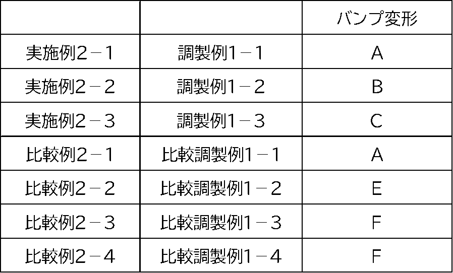
[7-1]積層体の作製
[実施例3-1]
デバイス側のウエハー(半導体基板)として100mmのシリコンウエハー(厚さ:770μm)に、調製例1-1で得られた接着剤組成物をスピンコートで塗布し、120℃で1.5分間加熱(前加熱処理)することにより、シリコンウエハーの回路面に積層体中の接着層の最終的な厚さが約60μmとなるように接着剤塗布層を形成した。
一方、キャリア側のウエハー(支持体)として100mmガラスウエハー(厚さ:500μm)に、調製例2で得られた剥離剤組成物をスピンコートで塗布し、250℃で5分間加熱することにより、ガラスウエハー上に積層体中の剥離層の最終的な厚さが約200nmとなるように剥離層を形成した。
その後、真空貼り合わせ装置内で、半導体基板と支持基板とを、接着剤塗布層及び剥離層を挟み込むように貼り合わせ、ホットプレート上で半導体基板側を下にして200℃で10分間加熱(後加熱処理)することにより積層体を作製した。なお、貼り合せは、温度23℃、減圧度1,000Paで行った。
調製例1-1で得られた接着剤組成物の代わりに、調製例1-2で得られた接着剤組成物を用いた以外は、実施例3-1と同様の方法で積層体を作製した。
調製例1-1で得られた接着剤組成物の代わりに、調製例1-3で得られた接着剤組成物を用いた以外は、実施例3-1と同様の方法で積層体を作製した。
レーザー照射装置を用いて、波長308nmのレーザーを、固定した積層体のガラスウエハー側から剥離層に300mJ/cm2で照射した。そして、支持基板をマニュアルで持ち上げることによって、剥離可否を確認した。その結果、実施例3-1、3-2、3-3で得られた各積層体においては、支持基板を持ち上げることにより負荷なく剥離することができた。
実施例で示す通り、調製例1-1~1-3で得られた接着剤組成物を用いて形成された接着層は、半導体基板と支持基板とを好適に接着させることができ、高温高圧下でバンプ変形を抑制することができ、さらに高いエッチングレートを示した。また、調製例1-1~1-3で得られた接着剤組成物を用いて形成された接着層は、半導体基板と支持基板との剥離も容易に行えるものであった。
比較調製例1-1で得られた接着剤組成物を用いて形成された接着層は、高温高圧下でバンプ変形を抑制することができるが、エッチングレートは低かった。比較調製例1-1の接着剤組成物に対して、剥離剤成分(B)を含有させた比較調製例1-3や1-4の接着剤組成物を用いて形成された接着層は、若干高めエッチングレートを示したが、高温高圧下でのバンプ変形を十分抑制することはできなかった。それに対して、比較調製例1-3や比較調製例1-4の接着剤組成物における上記式(V)で表される粘度200mPa・sのビニル基含有直鎖状ポリジメチルシロキサンや上記式(W)で表される粘度1000mPa・sのビニル基含有直鎖状ポリジメチルシロキサンを、上記式(V)で表される粘度100000mPa・sのビニル基含有直鎖状ポリジメチルシロキサンに替えた調製例1-1~1-3の接着剤組成物は、優れたバンプ変形抑制効果と高いエッチングレートを両立することができた。
調製例1-3で得られた接着剤組成物は、各比較調製例で得られた接着剤組成物に比べ、バンプ変形抑制効果とエッチングレートをバランスよく向上させることができた。そして、調製例1-2で得られた接着剤組成物は、作製後に多少の白濁が見られたが実用上問題はなく、バンプ変形抑制とエッチングレートに関しては、調製例1-3で得られた接着剤組成物に比べ、バンプ変形抑制効果とエッチングレートをより向上させることができた。さらに、調製例1-1で得られた接着剤組成物は、調製例1-2で得られた接着剤組成物と同様、高いエッチングレートを担保したまま、バンプ変形の個数を0とし調製例1-2で得られた接着剤組成物よりさらにバンプ変形抑制効果を向上させることができた。
1a バンプ
2 接着層
2a 接着剤塗布層
3 剥離層
4 支持基板
12 塗布装置
13 加熱装置
Claims (9)
- 接着剤成分(S)を含む接着剤組成物であって、
前記接着剤成分(S)は、ヒドロシリル化反応により硬化するポリオルガノシロキサン成分(A)を含有し、
前記ポリオルガノシロキサン成分(A)は、下記式(V)で表され、重量平均分子量が60,000以上である重合体(V)を含有する、接着剤組成物。
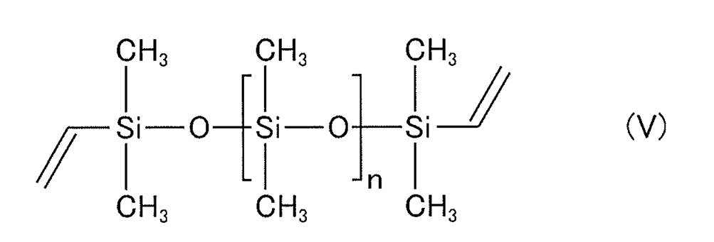
- 前記接着剤組成物が、前記接着剤成分(S)と、ポリオルガノシロキサンを含む剥離剤成分(B)とを含む、請求項1に記載の接着剤組成物。
- 前記ポリオルガノシロキサン成分(A)は、SiO2で表されるシロキサン単位(Q単位)、R1R2R3SiO1/2で表されるシロキサン単位(M単位)、R4R5SiO2/2で表されるシロキサン単位(D単位)及びR6SiO3/2で表されるシロキサン単位(T単位)からなる群より選ばれる1種又は2種以上の単位を含むポリオルガノシロキサン(A1)と、白金族金属系触媒(A2)とを含有し(ただし、R1~R6は、ケイ素原子に結合する基又は原子であり、それぞれ独立して、置換されていてもよいアルキル基、置換されていてもよいアルケニル基又は水素原子を表す)、
前記ポリオルガノシロキサン(A1)は、SiO2で表されるシロキサン単位(Q’単位)、R1’R2’R3’SiO1/2で表されるシロキサン単位(M’単位)、R4’R5’SiO2/2で表されるシロキサン単位(D’単位)及びR6’SiO3/2で表されるシロキサン単位(T’単位)からなる群より選ばれる1種又は2種以上の単位を含むとともに、前記M’単位、D’単位及びT’単位からなる群より選ばれる少なくとも1種を含むポリオルガノシロキサン(a1)と、SiO2で表されるシロキサン単位(Q”単位)、R1”R2”R3”SiO1/2で表されるシロキサン単位(M”単位)、R4”R5”SiO2/2で表されるシロキサン単位(D”単位)及びR6”SiO3/2で表されるシロキサン単位(T”単位)からなる群より選ばれる1種又は2種以上の単位を含むとともに、前記M”単位、D”単位及びT”単位からなる群より選ばれる少なくとも1種を含むポリオルガノシロキサン(a2)とを含み(ただし、R1’~R6’は、ケイ素原子に結合する基であり、それぞれ独立して、置換されていてもよいアルキル基又は置換されていてもよいアルケニル基を表すが、R1’~R6’の少なくとも1つは、置換されていてもよいアルケニル基であり、R1”~R6”は、ケイ素原子に結合する基又は原子であり、それぞれ独立して、置換されていてもよいアルキル基又は水素原子を表すが、R1”~R6”の少なくとも1つは、水素原子である)、
前記ポリオルガノシロキサン(a1)は、前記重合体(V)を含有する、請求項1又は2に記載の接着剤組成物。 - 前記重合体(V)の重量平均分子量が100,000以上である、請求項1~3のいずれか一項に記載の接着剤組成物。
- 前記剥離剤成分(B)の複素粘度が3400(Pa・s)以上である、請求項2に記載の接着剤組成物。
- 前記剥離剤成分(B)が、下記式(M1)で表されるポリオルガノシロキサンである、請求項5に記載の接着剤組成物。
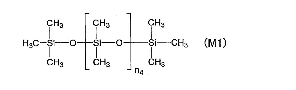
- バンプ付き半導体基板と支持基板との間に介在し、かつ前記半導体基板に接する接着層を備える積層体であって、
前記接着層が、請求項1~6のいずれか一項に記載の接着剤組成物から形成される層である、積層体。 - 請求項7に記載の積層体における前記半導体基板が加工される工程と、
前記支持基板と加工された前記半導体基板とが離される工程と、
を含む、半導体基板の製造方法。 - 請求項7に記載の積層体を製造する、積層体の製造方法であって、
前記接着層を与える接着剤塗布層が形成される工程と、
前記接着剤塗布層が加熱され、前記接着層が形成される工程と、
を含む、積層体の製造方法。
Priority Applications (5)
| Application Number | Priority Date | Filing Date | Title |
|---|---|---|---|
| JP2023508866A JPWO2022202153A1 (ja) | 2021-03-26 | 2022-03-01 | |
| KR1020237033218A KR20230161989A (ko) | 2021-03-26 | 2022-03-01 | 접착제 조성물, 적층체, 적층체의 제조 방법, 및 반도체 기판의 제조 방법 |
| US18/284,015 US20240182766A1 (en) | 2021-03-26 | 2022-03-01 | Adhesive composition, laminate, method for producing laminate, and method for producing semiconductor substrate |
| EP22774950.4A EP4317338A4 (en) | 2021-03-26 | 2022-03-01 | Adhesive composition, layered product, method for producing layered product, and method for producing semiconductor substrate |
| CN202280024274.7A CN117120573A (zh) | 2021-03-26 | 2022-03-01 | 粘接剂组合物、层叠体、层叠体的制造方法、以及半导体基板的制造方法 |
Applications Claiming Priority (2)
| Application Number | Priority Date | Filing Date | Title |
|---|---|---|---|
| JP2021-052890 | 2021-03-26 | ||
| JP2021052890 | 2021-03-26 |
Publications (1)
| Publication Number | Publication Date |
|---|---|
| WO2022202153A1 true WO2022202153A1 (ja) | 2022-09-29 |
Family
ID=83395582
Family Applications (1)
| Application Number | Title | Priority Date | Filing Date |
|---|---|---|---|
| PCT/JP2022/008678 Ceased WO2022202153A1 (ja) | 2021-03-26 | 2022-03-01 | 接着剤組成物、積層体、積層体の製造方法、及び半導体基板の製造方法 |
Country Status (7)
| Country | Link |
|---|---|
| US (1) | US20240182766A1 (ja) |
| EP (1) | EP4317338A4 (ja) |
| JP (1) | JPWO2022202153A1 (ja) |
| KR (1) | KR20230161989A (ja) |
| CN (1) | CN117120573A (ja) |
| TW (1) | TWI901856B (ja) |
| WO (1) | WO2022202153A1 (ja) |
Cited By (5)
| Publication number | Priority date | Publication date | Assignee | Title |
|---|---|---|---|---|
| WO2024154409A1 (ja) * | 2023-01-18 | 2024-07-25 | 日産化学株式会社 | 接着剤組成物、積層体、及び加工された半導体基板の製造方法 |
| WO2024185684A1 (ja) | 2023-03-08 | 2024-09-12 | 日産化学株式会社 | 接着剤組成物、積層体、及び加工された半導体基板の製造方法 |
| WO2024190698A1 (ja) * | 2023-03-10 | 2024-09-19 | 信越化学工業株式会社 | 仮接着材組成物及び基板の洗浄方法 |
| WO2024190396A1 (ja) | 2023-03-10 | 2024-09-19 | 日産化学株式会社 | 接着剤組成物、積層体、及び加工された半導体基板の製造方法 |
| WO2026094891A1 (ja) * | 2024-11-01 | 2026-05-07 | 日産化学株式会社 | 接着剤組成物、積層体、積層体の製造方法、及び加工された半導体基板又は電子デバイス基板の製造方法 |
Citations (10)
| Publication number | Priority date | Publication date | Assignee | Title |
|---|---|---|---|---|
| JP2002060719A (ja) * | 2000-08-21 | 2002-02-26 | Shin Etsu Chem Co Ltd | 接着性シリコーンゴム組成物及び半導体装置 |
| JP2007191629A (ja) * | 2006-01-20 | 2007-08-02 | Shin Etsu Chem Co Ltd | 熱硬化性組成物 |
| JP2011119427A (ja) * | 2009-12-03 | 2011-06-16 | Shin-Etsu Chemical Co Ltd | 積層型半導体集積装置の製造方法 |
| WO2016031551A1 (ja) * | 2014-08-29 | 2016-03-03 | 古河電気工業株式会社 | 導電性接着フィルム |
| WO2016181879A1 (ja) * | 2015-05-11 | 2016-11-17 | 富士フイルム株式会社 | 仮止め接着剤、接着フィルム、接着性支持体および積層体 |
| WO2017221772A1 (ja) | 2016-06-22 | 2017-12-28 | 日産化学工業株式会社 | ポリジメチルシロキサンを含有する接着剤 |
| WO2018216732A1 (ja) | 2017-05-24 | 2018-11-29 | 日産化学株式会社 | エポキシ変性ポリシロキサンを含有する仮接着剤 |
| WO2019088103A1 (ja) | 2017-11-01 | 2019-05-09 | 日産化学株式会社 | ノボラック樹脂を剥離層として含む積層体 |
| WO2020138240A1 (ja) * | 2018-12-27 | 2020-07-02 | 日産化学株式会社 | 光照射剥離用接着剤組成物及び積層体並びに積層体の製造方法及び剥離方法 |
| WO2021112070A1 (ja) * | 2019-12-02 | 2021-06-10 | 信越化学工業株式会社 | ウエハ加工用仮接着剤、ウエハ積層体及び薄型ウエハの製造方法 |
Family Cites Families (9)
| Publication number | Priority date | Publication date | Assignee | Title |
|---|---|---|---|---|
| JP5867383B2 (ja) * | 2012-12-21 | 2016-02-24 | 信越化学工業株式会社 | 付加硬化型自己接着性シリコーンゴム組成物 |
| DE102016201363A1 (de) * | 2016-01-29 | 2017-08-03 | Wacker Chemie Ag | Zu Silikongel vernetzbare Siliconzusammensetzung |
| US11028404B2 (en) * | 2018-07-27 | 2021-06-08 | Ut-Battelle, Llc | Methods of improving mycorrhization in plants and genetically modifed plants with improved mycorrhization |
| WO2020032286A1 (ja) * | 2018-08-10 | 2020-02-13 | ダウ・東レ株式会社 | 感圧接着層形成性オルガノポリシロキサン組成物およびその使用 |
| US11987731B2 (en) * | 2018-08-10 | 2024-05-21 | Dow Toray Co., Ltd. | Organopolysiloxane composition for forming pressure sensitive adhesive layer, and use of same |
| US11491064B2 (en) * | 2018-09-28 | 2022-11-08 | Stryker Corporation | Patient support having buckling elements for supporting a patient |
| US12227678B2 (en) * | 2018-11-16 | 2025-02-18 | Nissan Chemical Corporation | Laminate peeling method, laminate, and laminate production method |
| EP4015217A4 (en) * | 2019-08-13 | 2023-09-20 | Dow Toray Co., Ltd. | ORGANOPOLYSILOXANE COMPOSITION FOR FORMING A PRESSURE-SENSITIVE ADHESIVE LAYER, AND ASSOCIATED APPLICATION |
| WO2021131925A1 (ja) * | 2019-12-23 | 2021-07-01 | 日産化学株式会社 | 接着剤組成物、積層体及びその製造方法並びに積層体の剥離方法及び半導体形成基板を加工する方法 |
-
2022
- 2022-03-01 US US18/284,015 patent/US20240182766A1/en active Pending
- 2022-03-01 WO PCT/JP2022/008678 patent/WO2022202153A1/ja not_active Ceased
- 2022-03-01 EP EP22774950.4A patent/EP4317338A4/en active Pending
- 2022-03-01 KR KR1020237033218A patent/KR20230161989A/ko active Pending
- 2022-03-01 JP JP2023508866A patent/JPWO2022202153A1/ja active Pending
- 2022-03-01 CN CN202280024274.7A patent/CN117120573A/zh active Pending
- 2022-03-03 TW TW111107788A patent/TWI901856B/zh active
Patent Citations (10)
| Publication number | Priority date | Publication date | Assignee | Title |
|---|---|---|---|---|
| JP2002060719A (ja) * | 2000-08-21 | 2002-02-26 | Shin Etsu Chem Co Ltd | 接着性シリコーンゴム組成物及び半導体装置 |
| JP2007191629A (ja) * | 2006-01-20 | 2007-08-02 | Shin Etsu Chem Co Ltd | 熱硬化性組成物 |
| JP2011119427A (ja) * | 2009-12-03 | 2011-06-16 | Shin-Etsu Chemical Co Ltd | 積層型半導体集積装置の製造方法 |
| WO2016031551A1 (ja) * | 2014-08-29 | 2016-03-03 | 古河電気工業株式会社 | 導電性接着フィルム |
| WO2016181879A1 (ja) * | 2015-05-11 | 2016-11-17 | 富士フイルム株式会社 | 仮止め接着剤、接着フィルム、接着性支持体および積層体 |
| WO2017221772A1 (ja) | 2016-06-22 | 2017-12-28 | 日産化学工業株式会社 | ポリジメチルシロキサンを含有する接着剤 |
| WO2018216732A1 (ja) | 2017-05-24 | 2018-11-29 | 日産化学株式会社 | エポキシ変性ポリシロキサンを含有する仮接着剤 |
| WO2019088103A1 (ja) | 2017-11-01 | 2019-05-09 | 日産化学株式会社 | ノボラック樹脂を剥離層として含む積層体 |
| WO2020138240A1 (ja) * | 2018-12-27 | 2020-07-02 | 日産化学株式会社 | 光照射剥離用接着剤組成物及び積層体並びに積層体の製造方法及び剥離方法 |
| WO2021112070A1 (ja) * | 2019-12-02 | 2021-06-10 | 信越化学工業株式会社 | ウエハ加工用仮接着剤、ウエハ積層体及び薄型ウエハの製造方法 |
Non-Patent Citations (1)
| Title |
|---|
| See also references of EP4317338A4 |
Cited By (9)
| Publication number | Priority date | Publication date | Assignee | Title |
|---|---|---|---|---|
| WO2024154409A1 (ja) * | 2023-01-18 | 2024-07-25 | 日産化学株式会社 | 接着剤組成物、積層体、及び加工された半導体基板の製造方法 |
| WO2024185684A1 (ja) | 2023-03-08 | 2024-09-12 | 日産化学株式会社 | 接着剤組成物、積層体、及び加工された半導体基板の製造方法 |
| KR20250158742A (ko) | 2023-03-08 | 2025-11-06 | 닛산 가가쿠 가부시키가이샤 | 접착제 조성물, 적층체, 및 가공된 반도체 기판의 제조 방법 |
| EP4678708A1 (en) | 2023-03-08 | 2026-01-14 | Nissan Chemical Corporation | Adhesive composition, laminate, and method for producing processed semiconductor substrate |
| WO2024190698A1 (ja) * | 2023-03-10 | 2024-09-19 | 信越化学工業株式会社 | 仮接着材組成物及び基板の洗浄方法 |
| WO2024190396A1 (ja) | 2023-03-10 | 2024-09-19 | 日産化学株式会社 | 接着剤組成物、積層体、及び加工された半導体基板の製造方法 |
| KR20250157516A (ko) | 2023-03-10 | 2025-11-04 | 닛산 가가쿠 가부시키가이샤 | 접착제 조성물, 적층체, 및 가공된 반도체 기판의 제조 방법 |
| EP4678709A1 (en) | 2023-03-10 | 2026-01-14 | Nissan Chemical Corporation | Adhesive composition, laminate, and method for producing processed semiconductor substrate |
| WO2026094891A1 (ja) * | 2024-11-01 | 2026-05-07 | 日産化学株式会社 | 接着剤組成物、積層体、積層体の製造方法、及び加工された半導体基板又は電子デバイス基板の製造方法 |
Also Published As
| Publication number | Publication date |
|---|---|
| TWI901856B (zh) | 2025-10-21 |
| JPWO2022202153A1 (ja) | 2022-09-29 |
| EP4317338A4 (en) | 2025-04-09 |
| CN117120573A (zh) | 2023-11-24 |
| TW202237791A (zh) | 2022-10-01 |
| KR20230161989A (ko) | 2023-11-28 |
| EP4317338A1 (en) | 2024-02-07 |
| US20240182766A1 (en) | 2024-06-06 |
Similar Documents
| Publication | Publication Date | Title |
|---|---|---|
| US20240182766A1 (en) | Adhesive composition, laminate, method for producing laminate, and method for producing semiconductor substrate | |
| WO2023248872A1 (ja) | 光照射剥離用の剥離剤組成物 | |
| TWI862980B (zh) | 半導體基板之洗淨方法、加工後之半導體基板之製造方法、以及剝離及溶解用組成物 | |
| WO2023132229A1 (ja) | 接着剤組成物、積層体、積層体の製造方法、及び加工された基板の製造方法 | |
| CN120530177A (zh) | 粘接剂组合物、层叠体以及经加工的半导体基板的制造方法 | |
| KR20240105389A (ko) | 적층체, 박리제 조성물 및 가공된 반도체 기판의 제조 방법 | |
| TWI872179B (zh) | 接著劑組成物、積層體及其製造方法和積層體之剝離方法及半導體形成基板加工方法 | |
| EP4442785A1 (en) | Releasability imparter, adhesive composition, layered product, and method for producing semiconductor substrate | |
| CN117981055A (zh) | 半导体基板的清洗方法、经加工的半导体基板的制造方法以及剥离和溶解用组合物 | |
| WO2022210068A1 (ja) | 接着剤組成物、積層体、積層体の製造方法、及び加工された基板の製造方法 | |
| JP7852626B2 (ja) | 積層体、積層体の製造方法、及び半導体基板の製造方法 | |
| JP2022143089A (ja) | 積層体、積層体の製造方法、及び半導体基板の製造方法 | |
| US20240352281A1 (en) | Method of manufacturing laminate and kit of adhesive compositions | |
| JP7852292B2 (ja) | 光照射剥離用の接着剤組成物、積層体、積層体の製造方法、及び加工された半導体基板の製造方法 | |
| TWI917674B (zh) | 積層體之製造方法、及接著劑組成物之套組 | |
| WO2026094885A1 (ja) | 接着剤組成物、積層体、積層体の製造方法、及び加工された半導体基板又は電子デバイス基板の製造方法 | |
| WO2026079204A1 (ja) | 接着剤組成物、積層体、積層体の製造方法、及び加工された半導体基板又は電子デバイス基板の製造方法 | |
| WO2026094892A1 (ja) | 接着剤組成物、積層体、積層体の製造方法、及び加工された半導体基板の製造方法 | |
| CN119856258A (zh) | 半导体基板的清洗方法、经加工的半导体基板的制造方法以及剥离和溶解用组合物 | |
| WO2026094891A1 (ja) | 接着剤組成物、積層体、積層体の製造方法、及び加工された半導体基板又は電子デバイス基板の製造方法 | |
| TW202603116A (zh) | 接著劑組成物、積層體、積層體之製造方法、及加工後之半導體基板或電子裝置基板之製造方法 | |
| TW202603118A (zh) | 接著劑組成物、積層體、及加工後之半導體基板之製造方法 | |
| CN120731493A (zh) | 半导体基板的制造方法和经加工的半导体基板的制造方法以及剥离和溶解用组合物 | |
| TW202603117A (zh) | 接著劑組成物、積層體、及加工後之半導體基板之製造方法 | |
| KR20250068635A (ko) | 반도체 기판의 세정 방법, 가공된 반도체 기판의 제조 방법, 및 박리 및 용해용 조성물 |
Legal Events
| Date | Code | Title | Description |
|---|---|---|---|
| 121 | Ep: the epo has been informed by wipo that ep was designated in this application |
Ref document number: 22774950 Country of ref document: EP Kind code of ref document: A1 |
|
| WWE | Wipo information: entry into national phase |
Ref document number: 2023508866 Country of ref document: JP |
|
| WWE | Wipo information: entry into national phase |
Ref document number: 18284015 Country of ref document: US |
|
| WWE | Wipo information: entry into national phase |
Ref document number: 2022774950 Country of ref document: EP |
|
| NENP | Non-entry into the national phase |
Ref country code: DE |
|
| WWE | Wipo information: entry into national phase |
Ref document number: 11202307154W Country of ref document: SG |
|
| ENP | Entry into the national phase |
Ref document number: 2022774950 Country of ref document: EP Effective date: 20231026 |