WO2022209266A1 - 製造方法、検査方法、及び検査装置 - Google Patents
製造方法、検査方法、及び検査装置 Download PDFInfo
- Publication number
- WO2022209266A1 WO2022209266A1 PCT/JP2022/004078 JP2022004078W WO2022209266A1 WO 2022209266 A1 WO2022209266 A1 WO 2022209266A1 JP 2022004078 W JP2022004078 W JP 2022004078W WO 2022209266 A1 WO2022209266 A1 WO 2022209266A1
- Authority
- WO
- WIPO (PCT)
- Prior art keywords
- light
- layer
- emitting element
- electrically connected
- electrical connection
- Prior art date
- Legal status (The legal status is an assumption and is not a legal conclusion. Google has not performed a legal analysis and makes no representation as to the accuracy of the status listed.)
- Ceased
Links
Images


Classifications
-
- G—PHYSICS
- G01—MEASURING; TESTING
- G01R—MEASURING ELECTRIC VARIABLES; MEASURING MAGNETIC VARIABLES
- G01R31/00—Arrangements for testing electric properties; Arrangements for locating electric faults; Arrangements for electrical testing characterised by what is being tested not provided for elsewhere
- G01R31/26—Testing of individual semiconductor devices
- G01R31/2607—Circuits therefor
- G01R31/2632—Circuits therefor for testing diodes
- G01R31/2635—Testing light-emitting diodes, laser diodes or photodiodes
-
- H—ELECTRICITY
- H10—SEMICONDUCTOR DEVICES; ELECTRIC SOLID-STATE DEVICES NOT OTHERWISE PROVIDED FOR
- H10H—INORGANIC LIGHT-EMITTING SEMICONDUCTOR DEVICES HAVING POTENTIAL BARRIERS
- H10H20/00—Individual inorganic light-emitting semiconductor devices having potential barriers, e.g. light-emitting diodes [LED]
- H10H20/01—Manufacture or treatment
- H10H20/011—Manufacture or treatment of bodies, e.g. forming semiconductor layers
- H10H20/013—Manufacture or treatment of bodies, e.g. forming semiconductor layers having light-emitting regions comprising only Group III-V materials
- H10H20/0133—Manufacture or treatment of bodies, e.g. forming semiconductor layers having light-emitting regions comprising only Group III-V materials with a substrate not being Group III-V materials
- H10H20/01335—Manufacture or treatment of bodies, e.g. forming semiconductor layers having light-emitting regions comprising only Group III-V materials with a substrate not being Group III-V materials the light-emitting regions comprising nitride materials
-
- G—PHYSICS
- G01—MEASURING; TESTING
- G01N—INVESTIGATING OR ANALYSING MATERIALS BY DETERMINING THEIR CHEMICAL OR PHYSICAL PROPERTIES
- G01N21/00—Investigating or analysing materials by the use of optical means, i.e. using sub-millimetre waves, infrared, visible or ultraviolet light
- G01N21/17—Systems in which incident light is modified in accordance with the properties of the material investigated
- G01N21/55—Specular reflectivity
-
- G—PHYSICS
- G01—MEASURING; TESTING
- G01N—INVESTIGATING OR ANALYSING MATERIALS BY DETERMINING THEIR CHEMICAL OR PHYSICAL PROPERTIES
- G01N21/00—Investigating or analysing materials by the use of optical means, i.e. using sub-millimetre waves, infrared, visible or ultraviolet light
- G01N21/84—Systems specially adapted for particular applications
- G01N21/88—Investigating the presence of flaws or contamination
- G01N21/95—Investigating the presence of flaws or contamination characterised by the material or shape of the object to be examined
- G01N21/9501—Semiconductor wafers
-
- G—PHYSICS
- G01—MEASURING; TESTING
- G01N—INVESTIGATING OR ANALYSING MATERIALS BY DETERMINING THEIR CHEMICAL OR PHYSICAL PROPERTIES
- G01N21/00—Investigating or analysing materials by the use of optical means, i.e. using sub-millimetre waves, infrared, visible or ultraviolet light
- G01N21/84—Systems specially adapted for particular applications
- G01N21/88—Investigating the presence of flaws or contamination
- G01N21/95—Investigating the presence of flaws or contamination characterised by the material or shape of the object to be examined
- G01N21/956—Inspecting patterns on the surface of objects
-
- G—PHYSICS
- G01—MEASURING; TESTING
- G01R—MEASURING ELECTRIC VARIABLES; MEASURING MAGNETIC VARIABLES
- G01R31/00—Arrangements for testing electric properties; Arrangements for locating electric faults; Arrangements for electrical testing characterised by what is being tested not provided for elsewhere
- G01R31/26—Testing of individual semiconductor devices
- G01R31/265—Contactless testing
- G01R31/2656—Contactless testing using non-ionising electromagnetic radiation, e.g. optical radiation
-
- H—ELECTRICITY
- H10—SEMICONDUCTOR DEVICES; ELECTRIC SOLID-STATE DEVICES NOT OTHERWISE PROVIDED FOR
- H10H—INORGANIC LIGHT-EMITTING SEMICONDUCTOR DEVICES HAVING POTENTIAL BARRIERS
- H10H20/00—Individual inorganic light-emitting semiconductor devices having potential barriers, e.g. light-emitting diodes [LED]
- H10H20/01—Manufacture or treatment
-
- H—ELECTRICITY
- H10—SEMICONDUCTOR DEVICES; ELECTRIC SOLID-STATE DEVICES NOT OTHERWISE PROVIDED FOR
- H10H—INORGANIC LIGHT-EMITTING SEMICONDUCTOR DEVICES HAVING POTENTIAL BARRIERS
- H10H20/00—Individual inorganic light-emitting semiconductor devices having potential barriers, e.g. light-emitting diodes [LED]
- H10H20/80—Constructional details
- H10H20/81—Bodies
- H10H20/815—Bodies having stress relaxation structures, e.g. buffer layers
-
- H—ELECTRICITY
- H10—SEMICONDUCTOR DEVICES; ELECTRIC SOLID-STATE DEVICES NOT OTHERWISE PROVIDED FOR
- H10H—INORGANIC LIGHT-EMITTING SEMICONDUCTOR DEVICES HAVING POTENTIAL BARRIERS
- H10H20/00—Individual inorganic light-emitting semiconductor devices having potential barriers, e.g. light-emitting diodes [LED]
- H10H20/80—Constructional details
- H10H20/81—Bodies
- H10H20/822—Materials of the light-emitting regions
- H10H20/824—Materials of the light-emitting regions comprising only Group III-V materials, e.g. GaP
- H10H20/825—Materials of the light-emitting regions comprising only Group III-V materials, e.g. GaP containing nitrogen, e.g. GaN
-
- H—ELECTRICITY
- H10—SEMICONDUCTOR DEVICES; ELECTRIC SOLID-STATE DEVICES NOT OTHERWISE PROVIDED FOR
- H10H—INORGANIC LIGHT-EMITTING SEMICONDUCTOR DEVICES HAVING POTENTIAL BARRIERS
- H10H20/00—Individual inorganic light-emitting semiconductor devices having potential barriers, e.g. light-emitting diodes [LED]
- H10H20/80—Constructional details
- H10H20/84—Coatings, e.g. passivation layers or antireflective coatings
-
- H—ELECTRICITY
- H10—SEMICONDUCTOR DEVICES; ELECTRIC SOLID-STATE DEVICES NOT OTHERWISE PROVIDED FOR
- H10H—INORGANIC LIGHT-EMITTING SEMICONDUCTOR DEVICES HAVING POTENTIAL BARRIERS
- H10H29/00—Integrated devices, or assemblies of multiple devices, comprising at least one light-emitting semiconductor element covered by group H10H20/00
- H10H29/01—Manufacture or treatment
- H10H29/032—Manufacture or treatment of electrodes
-
- H—ELECTRICITY
- H10—SEMICONDUCTOR DEVICES; ELECTRIC SOLID-STATE DEVICES NOT OTHERWISE PROVIDED FOR
- H10P—GENERIC PROCESSES OR APPARATUS FOR THE MANUFACTURE OR TREATMENT OF DEVICES COVERED BY CLASS H10
- H10P74/00—Testing or measuring during manufacture or treatment of wafers, substrates or devices
- H10P74/20—Testing or measuring during manufacture or treatment of wafers, substrates or devices characterised by the properties tested or measured, e.g. structural or electrical properties
- H10P74/203—Structural properties, e.g. testing or measuring thicknesses, line widths, warpage, bond strengths or physical defects
Definitions
- One aspect of the present invention relates to a semiconductor device manufacturing method, an inspection method, and an inspection apparatus.
- the method of observing photoluminescence as described above can detect leakage defects, contact defects (open defects, high-resistance defects, and high-threshold defects) cannot be detected appropriately. Therefore, in the method of observing photoluminescence as described above, defective products (light emitting devices with poor contact) may be included in the light emitting devices that are determined to be good products because they are not leak defective. It may not be possible to appropriately determine whether the light emitting element is good or bad.
- An aspect of the present invention has been made in view of the above circumstances, and an object of the present invention is to appropriately detect contact failure of a light-emitting element.
- a method of manufacturing a semiconductor device is a method of manufacturing a semiconductor device in which a plurality of light emitting elements are formed, wherein crystals are grown on a substrate to form a buffer layer, an N layer, a light emitting layer, and a P layer, an insulating film is formed on the laminated film, contact holes are formed in the insulating film at an electrical connection portion of the N layer and an electrical connection portion of the P layer, and the first member is formed.
- a laminated film and an insulating film are formed, contact holes are formed in the insulating film at an electrical connection portion of the N layer and an electrical connection portion of the P layer, and the insulating film is
- the second member on which the conductive layer is formed is irradiated with light, and the second member generates The emitted light is measured.
- the electrical connection portion of the N layer and the electrical connection portion of the P layer are electrically connected to each other by the conductive layer, and are in a short-circuited state.
- recombination of carriers is less likely to occur in the portion that becomes a non-defective light-emitting element, resulting in low emission luminance.
- the portion of the light emitting element with poor contact even if the electrically connected portion of the N layer and the electrically connected portion of the P layer are electrically connected to each other by the conductive layer (short-circuited state).
- the emission luminance is higher than that of a non-defective product.
- the luminance of light emitted from the second member in a state where the electrically connected portion of the N layer and the electrically connected portion of the P layer are electrically connected to each other by the conductive layer depends on the presence or absence of contact failure. Differences occur. Therefore, as in the manufacturing method according to one aspect of the present invention, the second member in which the electrically connected portion of the N layer and the electrically connected portion of the P layer are electrically connected to each other by the conductive layer is irradiated with light.
- contact failure can be detected in the semiconductor device manufacturing process. Contact failures can be detected easily and quickly as compared with the case (inspection is performed separately outside the manufacturing process).
- the above manufacturing method may further comprise, after the fourth step, a fifth step of irradiating the semiconductor device with light and measuring the light emitted from the semiconductor device.
- the semiconductor device produced through the fourth step the first pad electrode and the second pad electrode are formed, and the electrical connection portion of the N layer and the electrical connection portion of the P layer are electrically connected to each other. do not have.
- the brightness of light emitted from such a semiconductor device varies depending on the presence or absence of leakage defects. For this reason, by irradiating the semiconductor device after the fourth step with light and measuring the light emission from the semiconductor device, based on the luminance of the measured light emission, the portion of the light emitting element with the leak defect and the light emission without the leak defect can be determined. It becomes possible to distinguish from the part of the element. This makes it possible to appropriately detect leakage defects in the light emitting element.
- the part of the light emitting element with the contact failure is specified based on the measurement result in the third step, and the part of the light emitting element with the leakage failure is specified based on the measurement result in the fifth step.
- the method may further include a sixth step of discriminating between non-defective and defective light-emitting elements based on the specified result. According to such a configuration, it is possible to appropriately detect a light-emitting element with a contact failure and a light-emitting element with a leak failure as defective products, and improve the accuracy of determining whether the light-emitting element is good or bad.
- the semiconductor device in the reflected image is obtained based on the reflected image obtained by irradiating the second member with light and measuring the reflected light from the second member, and the design data of the semiconductor device obtained in advance.
- a seventh step of identifying a location corresponding to each light emitting element of the device may also be included. As a result, it is possible to determine from which light emitting element on the design data the light is emitted when the light emission is measured.
- An inspection method is a measurement object in which a plurality of light-emitting elements are being formed, wherein an electrical connection portion of an N layer and an electrical connection portion of a P layer in an insulating film on a laminated film are electrically connected to each other.
- the measurement object is irradiated with light in a state in which the electrically connected portion of the N layer and the electrically connected portion of the P layer are electrically connected to each other by the conductive layer.
- Light emission from the measurement object is measured.
- the state in which the electrical connection portion of the N layer and the electrical connection portion of the P layer are electrically connected to each other is a short-circuited state. In such a short-circuited object to be measured, recombination of carriers is less likely to occur in a portion that becomes a non-defective light-emitting element, resulting in low emission luminance.
- the portion of the light emitting element with poor contact even if the electrically connected portion of the N layer and the electrically connected portion of the P layer are electrically connected to each other by the conductive layer (short-circuited state). Since recombination of carriers occurs actively inside, the emission luminance is higher than that of a non-defective product. In this way, the luminance of light emitted from the measurement object in a state in which the electrically connected portion of the N layer and the electrically connected portion of the P layer are electrically connected to each other by the conductive layer depends on the presence or absence of contact failure. Differences occur.
- the inspection method As in the inspection method according to one aspect of the present invention, light is applied to the measurement object in which the electrically connected portion of the N layer and the electrically connected portion of the P layer are electrically connected to each other by the conductive layer.
- the measurement object By measuring the light emission from the measurement object, it becomes possible to distinguish between the light emitting element portion with poor contact and the light emitting device portion without contact failure based on the luminance of the measured light emission. .
- the object to be measured in a state in which the conductive layer is processed so that the electrical connection portion of the N layer and the electrical connection portion of the P layer are not electrically connected to each other, the object to be measured is irradiated with light, and the object to be measured is may further include a second measurement step of measuring the light emission generated at .
- the luminance of light emitted from a semiconductor device in which the electrically connected portion of the N layer and the electrically connected portion of the P layer are not electrically connected to each other varies depending on the presence or absence of leakage defects.
- the portion of the light emitting element having the contact failure is specified based on the measurement result in the first measurement step, and the portion of the light emitting element having the leakage failure is specified based on the measurement result of the second measurement step, A determination step of determining whether the light-emitting element is good or bad based on the identification result may be further included. According to such a configuration, it is possible to appropriately detect a light-emitting element with a contact failure and a light-emitting element with a leak failure as defective products, and improve the accuracy of determining whether the light-emitting element is good or bad.
- the reflected image A specifying step of specifying a position corresponding to each light emitting element of the measurement object may be further included.
- An inspection apparatus includes a light irradiation unit that irradiates light onto a measurement object being formed by a plurality of light-emitting elements, and light emitted from the measurement object according to the light irradiated by the light irradiation unit.
- An optical measurement unit that measures light emission, and a processing unit that outputs measurement results obtained by the optical measurement unit.
- a measurement result obtained by the optical measurement unit is output in a state in which the conductive layer is formed so that the electrical connection point of the layer and the electrical connection point of the P layer are electrically connected to each other.
- the light emission from the object to be measured in the state where the electrical connection point of the N layer and the electrical connection point of the P layer are electrically connected to each other depends on the presence or absence of contact failure. A difference occurs in the luminance.
- optical measurement in a state in which a conductive layer is formed and the electrical connection portion of the N layer and the electrical connection portion of the P layer are electrically connected to each other By outputting the result of measurement by the part, it becomes possible to distinguish between the part of the light emitting element with defective contact and the light emitting element with no defective contact based on the measured luminance of light emission. As a result, it is possible to appropriately detect the contact failure of the light-emitting element and improve the accuracy of determining the quality of the light-emitting element.
- the processing unit may output the result of measurement by the optical measurement unit in a state in which the electrically conductive layer is processed so that the electrically connected portion of the N layer and the electrically connected portion of the P layer are not electrically connected to each other.
- the brightness of the light emitted from the object to be measured in a state in which the electrically connected portion of the N layer and the electrically connected portion of the P layer are not electrically connected to each other varies depending on the presence or absence of leakage defects. occur. Therefore, by outputting the measurement result of the optical measurement unit in a state in which the electrically connected portion of the N layer and the electrically connected portion of the P layer are not electrically connected to each other, the luminance of the light emission is measured. Therefore, it becomes possible to distinguish between the portion of the light emitting element that has a leak defect and the portion of the light emitting element that does not have a leak defect. This makes it possible to appropriately detect leakage defects in the light emitting element.
- the processing unit identifies the portion of the light emitting element with poor contact based on the measurement result by the optical measurement unit in a state where the electrical connection portion of the N layer and the electrical connection portion of the P layer are electrically connected to each other. At the same time, the part of the light emitting element having a leak defect is specified based on the measurement result by the optical measurement unit in a state where the electrical connection part of the N layer and the electrical connection part of the P layer are not electrically connected to each other. Based on the results, it is also possible to determine whether the light-emitting elements are good or bad.
- the light measurement unit further measures reflected light from the measurement object according to the light irradiated by the light irradiation unit, and the processing unit measures a reflected light obtained by measuring the reflected light in the light measurement unit, and A position corresponding to each light-emitting element of the measurement object in the reflected image may be specified based on design data of the measurement object acquired in advance. As a result, it is possible to determine from which light emitting element on the design data the light is emitted when the light emission is measured.
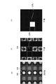
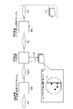
- FIG. 1 is a configuration diagram of an inspection device 1 according to an embodiment of the present invention
- FIG. It is a figure which shows the imaging result by a camera, (a) is a reflected image, (b) is a PL image which shows leak failure, (c) is a PL image which shows contact failure.
- It is a figure explaining the manufacturing process of a semiconductor device. It is a figure explaining the manufacturing process of a semiconductor device. It is a figure explaining the manufacture of a semiconductor device, and an inspection process. It is a figure explaining the manufacture of a semiconductor device, and an inspection process. It is a flow chart which shows the procedure of the manufacturing method of a semiconductor device.
- FIG. 1 is a configuration diagram of an inspection apparatus 1 according to this embodiment.
- the inspection apparatus 1 is an apparatus for inspecting a sample S (object to be measured).
- a sample S is a semiconductor device in which a plurality of light emitting elements are formed on a wafer.
- the sample S (object to be measured) described in this embodiment includes not only completed semiconductor devices but also semiconductor devices that are being manufactured (unfinished).
- a light-emitting element may be in the process of being formed, and terms that refer to such a light-emitting element being formed include, for example, "portion to become the light-emitting element" and "portion of the light-emitting element".
- the inspection apparatus 1 observes photoluminescence (specifically, fluorescence) for each of the plurality of light-emitting elements formed in the sample S to determine whether the defective product corresponds to a contact failure or a leak failure, or , to determine whether the product is acceptable. It is also conceivable to inspect such light-emitting elements by probing, for example (that is, based on electrical characteristics).
- the method for inspecting a light-emitting element based on photoluminescence can perform inspection by acquiring a fluorescence image. can be inspected.
- the inspection apparatus 1 includes a chuck 11, an XY stage 12, an excitation light source 20 (light irradiation section), an optical system 30, a dichroic mirror 40, an objective lens 51, and a Z stage 52. , an imaging lens 72 , a camera 82 (optical measurement section), a dark box 90 , a control device 100 (processing section), and a monitor 110 .
- the dark box 90 accommodates, for example, the components other than the control device 100 and the monitor 110 among the components described above, and is provided to avoid the influence of external light on each component accommodated.
- each component housed in the dark box 90 may be mounted on a vibration isolation table in order to improve the quality of the image captured by the camera 82 (improvement of image quality and prevention of positional deviation of the image).
- the chuck 11 is a holding member that holds the sample S.
- the chuck 11 holds the sample S by vacuum-sucking the wafer of the sample S, for example.
- the XY stage 12 is a stage that moves the chuck 11 holding the sample S in the XY directions (front-rear and left-right directions), that is, in directions along the mounting surface of the sample S on the chuck 11 .
- the XY stage 12 moves the chuck 11 in the XY directions under the control of the control device 100 so that each of the plurality of light emitting elements sequentially becomes the irradiation region of the excitation light.
- the inspection apparatus 1 may further include a rotation stage ( ⁇ stage; not shown).
- Such a rotating stage may be provided above the XY stage 12 and below the chuck 11 , or may be provided integrally with the XY stage 12 .
- the rotating stage is for aligning the vertical and horizontal positions of the sample S with high accuracy. By providing the rotating stage, it is possible to shorten the time for alignment and the like, and shorten the total time for data processing.
- the excitation light source 20 is a light irradiation unit that generates excitation light to irradiate the sample S and irradiates the sample S with the excitation light.
- the excitation light source 20 may be any light source capable of generating light having a wavelength that excites the light emitting element of the sample S, such as an LED, a laser, a halogen lamp, a mercury lamp, a D2 lamp, a plasma light source, or the like.
- the inspection apparatus 1 may further include a sensor that monitors the illumination luminance in order to keep the luminance of the excitation light emitted from the excitation light source 20 constant. Further, in order to reduce shading as much as possible, a diffusion plate, a fly-eye lens, or the like may be used at the position where the excitation light is emitted from the excitation light source 20 to homogenize the luminance distribution.
- the optical system 30 includes an optical fiber cable 31 and a light guide lens 32 .
- the optical fiber cable 31 is a light-guiding optical fiber cable connected to the excitation light source 20 .
- the light guide lens 32 is, for example, a single or compound convex lens, and guides the excitation light arriving via the optical fiber cable 31 toward the dichroic mirror 40 .
- the inspection apparatus 1 includes a bandpass filter (not shown) between the excitation light source 20 and the dichroic mirror 40. may
- the dichroic mirror 40 is a mirror made using a special optical material that reflects light of a specific wavelength and transmits light of other wavelengths. Specifically, the dichroic mirror 40 reflects the excitation light in the direction of the objective lens 51 and transmits photoluminescence (more specifically, fluorescence) from the light-emitting element, which is light in a wavelength band different from that of the excitation light, to the imaging lens 72 . It is configured to transmit in all directions.
- the region of the normal emission spectrum of excitation light may be on the lower wavelength side than the region of the normal emission spectrum of fluorescence (normal fluorescence spectrum). That is, the dichroic mirror 40 reflects excitation light, which is light in a low wavelength band, toward the objective lens 51 , and transmits fluorescent light, which is light in a higher wavelength band than the excitation light, toward the imaging lens 72 .
- the objective lens 51 is configured to observe the sample S, and collects the excitation light guided by the dichroic mirror 40 onto the sample S.
- the Z stage 52 moves the objective lens 51 in the Z direction (vertical direction), that is, in a direction intersecting the mounting surface of the sample S on the chuck 11 to perform focus adjustment.
- the imaging lens 72 is a lens that forms an image of the fluorescence of the light-emitting element that has passed through the dichroic mirror 40 and guides the fluorescence to the camera 82 .
- a camera 82 captures the fluorescence of the light emitting element. That is, the camera 82 performs measurement by capturing the luminescence (fluorescence) generated in the sample S in response to the excitation light emitted by the excitation light source 20 .
- Camera 82 detects the image formed by imaging lens 72 .
- the camera 82 outputs a PL image (fluorescence image), which is the imaging result, to the control device 100 .
- the camera 82 is, for example, an area image sensor such as CCD or MOS.
- the camera 82 may be configured by a line sensor or a TDI sensor. Note that the camera 82 also captures (measures) reflected light from the sample S corresponding to the excitation light applied to the sample S by the excitation light source 20, as will be described later.
- the control device 100 controls the XY stage 12, the excitation light source 20, the Z stage 52, and the camera 82. Specifically, the controller 100 controls the XY stage 12 to adjust the irradiation area of the excitation light (irradiation area on the sample S). The controller 100 controls the Z stage 52 to adjust the focus of the excitation light. The control device 100 controls the pumping light source 20 to adjust the emission of the pumping light and adjust the wavelength, amplitude, and the like of the pumping light. The control device 100 controls the camera 82 to make adjustments related to acquisition of fluorescence images. In addition, the control device 100 determines the quality of the light-emitting element based on the fluorescence image captured by the camera 82 (details will be described later).
- control device 100 is a computer, and physically includes memories such as RAM and ROM, a processor (arithmetic circuit) such as a CPU, a communication interface, and a storage unit such as a hard disk. Examples of the control device 100 include personal computers, cloud servers, smart devices (smartphones, tablet terminals, etc.).
- the control device 100 functions by causing the CPU of the computer system to execute a program stored in memory.
- a monitor 110 is a display device that displays a PL image (fluorescence image) or the like, which is a measurement result.
- FIG. 3 A semiconductor device manufacturing process is performed in a manufacturing apparatus 500 (see FIG. 5).
- a sapphire substrate 401 is prepared as shown in FIG. 3(a).
- the sapphire substrate 401 may be produced through, for example, a single crystal growth process for producing an ingot, a processing process for thinly slicing the sapphire ingot, and a CMP (Chemical Mechanical Polishing) process for polishing flat.
- a substrate made of another material suitable for the semiconductor may be used instead of the sapphire substrate 401.
- an epitaxial growth process is performed on the sapphire substrate 401.
- a buffer layer 402 (see FIG. 3(b)), an n-GaN layer 403 (see FIG. 3(c)) as an electron transport layer, and a light emitting layer are formed.
- a laminated film is formed comprising a layer 404 (see FIG. 3(d)) and a p-GaN layer 405 (see FIG. 3(e)) which is a hole transport layer.
- the epitaxial growth step may be performed by, for example, LPE (Liquid Phase Epitaxy) method or MOVPE (Metal Organic Vapor Phase Epitaxy) method.
- the electron-transporting layer and the hole-transporting layer are not necessarily made of GaN, and may be a semiconductor containing another element that does not cause mismatch in band energy and lattice spacing with the light-emitting layer 404 . Also, the positions of the n-GaN layer 403 and the p-GaN layer 405 may be opposite to each other.
- element isolation is performed. Specifically, resist application, patterning, etching, and resist removal are sequentially performed.
- FIG. 4(a) a process for exposing the n-GaN layer 403 is performed. Specifically, resist application, patterning, etching, and resist removal are sequentially performed. The order of the element isolation process shown in FIG. 3F and the process shown in FIG. 4A may be reversed.
- an insulating film 406 is formed on the laminated film.
- contact holes H1 and H2 are formed through the insulating film 406 at predetermined locations in the insulating film 406.
- a contact hole H ⁇ b>1 is formed in the insulating film 406 where the n-GaN layer 403 is electrically connected.
- a contact hole H2 is formed in the insulating film 406 at a location where the p-GaN layer 405 is electrically connected.
- the member produced by the steps up to this point is the first member S1.
- a conductive layer 407 is formed on the surface of the first member S1 on which the insulating film 406 is formed, as shown in FIG. 4(d).
- the conductive layer 407 is an electrode material, such as metal or ITO (Indium Tin Oxide).
- the conductive layer 407 is formed over substantially the entire surface on which the insulating film 406 is formed. Therefore, the conductive layer 407 electrically connects (conducts) the electrical connection portion of the n-GaN layer 403 and the electrical connection portion of the p-GaN layer 405 to each other.
- the member produced by the steps up to this point is the second member S2.
- the first pad electrode 407A corresponding to the electrical connection portion of the n-GaN layer 403 and the p-GaN layer 405 are electrically connected.
- a second pad electrode 407B corresponding to the location is formed.
- resist application, patterning, etching, and resist removal are sequentially performed to form the first pad electrode 407A and the second pad electrode 407B.
- the electrical connection portion of the n-GaN layer 403 and the electrical connection portion of the p-GaN layer 405 are electrically connected to each other. do not have.
- the above is the manufacturing process of the semiconductor device.
- FIG. 5 is a diagram illustrating an example of manufacturing and inspection processes of a semiconductor device.
- the sapphire substrate 401 undergoes an epitaxial growth process (see FIGS. 3B to 3E), element isolation (see FIG. 3F), A process of exposing the n-GaN layer 403 (see FIG. 4A), a process of forming the insulating film 406 (see FIG. 4B), and a process of forming the contact holes H1 and H2 (see FIG. 4C). ), a conductive layer forming process (see FIG. 4D) for forming the conductive layer 407 is performed to generate the second member S2.
- the second member S2 is used as the sample S, and a first measurement step (details will be described later) of PL measurement for the second member S2 is performed.
- a first measurement step (details will be described later) of PL measurement for the second member S2 is performed.
- the contact failure position on the second member S2 is specified, and data D1 indicating the contact failure position is output.
- the processes after the pad forming process (see FIG. 4E) for forming the first pad electrode 407A and the second pad electrode 407B are performed on the second member S2 to produce the semiconductor device S3. be.
- the first measurement step which is the PL measurement for specifying the contact failure position, is performed.
- the first measurement step is a step related to detection of a light-emitting element with poor contact.
- the second member S2 which is the object to be measured, is irradiated with light, and the second member S2 is irradiated with light. This is the step of measuring the emitted light.
- the excitation light emitted from the excitation light source 20 is applied to the surface (back surface) of the second member S2 on which the conductive layer 407 is not formed. ).
- the excitation light may be irradiated from the surface (surface) on the conductive layer 407 side.
- Light emitted from the second member S2 in response to the excitation light is transmitted through the dichroic mirror 40, formed into an image by the imaging lens 72, and detected (measured) by the camera 82 as a PL image.
- the controller 100 controls the camera 82 in a state in which the conductive layer 407 is formed such that the electrical connection portion of the n-GaN layer 403 and the electrical connection portion of the p-GaN layer 405 are electrically connected to each other.
- a detection (measurement) result is output for a determination step to be described later.
- the determination step is performed by the control device 100.
- the control device 100 identifies the light-emitting element with poor contact based on the measurement result in the first measurement step.
- the control device 100 identifies the luminance of each light emitting element in the PL image, and identifies the light emitting element with poor contact based on the luminance. In the PL image of FIG. 2(c), only the luminance of a certain light emitting element 200z is higher than the luminance of the other light emitting elements.
- control device 100 identifies the light emitting element 200z as a light emitting element with poor contact.
- the control device 100 generates and outputs data D1, which is a contact failure map defining addresses (positions) of light emitting elements with contact failure.
- the control device 100 based on the data D1, which is the measurement result in the first measurement step, the control device 100 identifies the light-emitting element having the contact failure in the semiconductor device S3 as a defective product, and outputs the address of the defective light-emitting element. .
- defective light emitting elements are not used in subsequent processes, and the quality of panels and the like using light emitting elements can be improved.
- FIG. 6 is a diagram explaining another example of the manufacturing and inspection process of a semiconductor device.
- the semiconductor device S3 subjected to the pad forming process is used as the sample S, and the second measurement step is performed. Further, a determination step corresponding to the second measurement step is performed.
- the second measurement step is a step related to detection of a light emitting element with a leak defect, and a pad forming process is performed so that an electrical connection portion of the n-GaN layer 403 and an electrical connection portion of the p-GaN layer 405 are formed.
- This is a step of irradiating the semiconductor devices S3 that are not electrically connected to each other with light and measuring the luminescence generated in the semiconductor devices S3.
- the semiconductor device S3 is irradiated with excitation light emitted from the excitation light source 20 while the semiconductor device S3 is placed on the chuck 11 .
- the control device 100 displays the detection (measurement) result by the camera 82 in a state in which the electrical connection portion of the n-GaN layer 403 and the electrical connection portion of the p-GaN layer 405 are not electrically connected to each other, which will be described later. output for the decision step.
- the control device 100 identifies the light emitting element with the contact failure based on the measurement result in the first measurement step, and identifies the light emitting element with the leakage failure based on the measurement result in the second measurement step, A non-defective light-emitting element and a defective light-emitting element are discriminated based on the identification result. Identification of contact failure is as described above.
- the control device 100 identifies the luminance of each light emitting element in the PL image, and identifies the light emitting element with the leak failure based on the luminance.
- the control device 100 identifies the light emitting element 200x as a light emitting element with a leak failure.
- the control device 100 generates and outputs data D2, which is a leak defect map that defines the addresses (positions) of light emitting elements with leak defects.
- the control device 100 identifies the light emitting element with the contact failure based on the data D1, which is the measurement result in the first measurement step, and specifies the leak failure based on the data D2, which is the measurement result in the second measurement step.
- a light-emitting element is specified, and a non-defective light-emitting element and a defective light-emitting element are discriminated based on the result of the specification.
- the control device 100 specifies the light emitting elements that are not defective in contact and not defective in leakage, determines the light emitting elements to be non-defective, and determines the other light emitting elements. The defective product is determined, and the address of the defective light emitting element is output.
- the defective light emitting element can be removed by the laser device 600 (see FIG. 6).
- the semiconductor device S4 see FIG. 6) can be produced from which the defective light emitting element is removed.
- a specific step of aligning the light emitting elements may be performed before performing the first measurement step and the second measurement step.
- the identification step based on the reflected image obtained by irradiating the sample S with light and measuring the reflected light from the sample S and the design data of the sample S acquired in advance, each of the samples S in the reflected image Identify the position corresponding to the light emitting element (align the light emitting element).
- the second member S2 is irradiated with light emitted from the excitation light source 20, and the reflected light is detected by the camera 82 and reflected image (for example, shown in FIG. 2(a) image) is obtained.
- the semiconductor device S3 is irradiated with light emitted from the excitation light source 20, the reflected light is detected by the camera 82, and the reflected image (for example, as shown in FIG. 2(a) image) is obtained.
- the reflected image shows an image corresponding to each light emitting element 200 and each electrode 300 .
- the control device 100 identifies the position corresponding to each light emitting element of the sample S in the reflected image by comparing the reflected image with the design data of the sample S.
- the design data here indicates at least the state (position, shape, etc.) of each light emitting element and electrode of the sample S.
- each light emitting element of the sample S is specified at which position in the acquired image, so that in the first measurement step and the second measurement step It is possible to specify which light-emitting element each position of the acquired PL image corresponds to.
- FIG. 7 is a flow chart showing the steps of the method for manufacturing the semiconductor device S4.
- an epitaxial growth step is performed to grow crystals on a sapphire substrate 401 to form a buffer layer 402, an n-GaN layer 403, a light emitting layer 404 and a p-GaN layer 405. is formed, an insulating film 406 is formed on the laminated film, a contact hole H1 is formed in the insulating film 406 at an electrical connection portion of the n-GaN layer 403, and p - A contact hole H2 is formed at the electrical connection point of the GaN layer 405 (first step, step S101).
- a first member S1 is generated by the first step.
- a conductive layer 407 is formed on the entire surface of the first member S1 on which the insulating film 406 is formed (second step, step S102).
- the second step produces a second member S2 in which the electrical connection points of the n-GaN layer 403 and the electrical connection points of the p-GaN layer 405 are electrically connected to each other by the conductive layer 407 .
- control device 100 identifies the luminance of each light emitting element in the PL image, and identifies the light emitting element with poor contact based on the luminance.
- the control device 100 generates and outputs data D1, which is a contact failure map defining addresses (positions) of light emitting elements with contact failure.
- the first pad electrode 407A corresponding to the electrical connection portion of the n-GaN layer 403 and the p-GaN layer 405 are electrically connected.
- a second pad electrode 407B corresponding to the location is formed (fourth step, step S104).
- step S105 PL measurement is performed by irradiating the semiconductor device S3 with excitation light and measuring the light emission generated in the semiconductor device S3 (fifth step, step S105).
- the control device 100 identifies the luminance of each light emitting element in the PL image, and identifies the light emitting element with the leak failure based on the luminance.
- the control device 100 generates and outputs data D2, which is a leak defect map that defines the addresses (positions) of light emitting elements with leak defects.
- a light emitting element with a contact failure is identified based on the data D1
- a light emitting element with a leak failure is identified based on the data D2
- good and defective light emitting elements are identified based on the identification results. It is determined (sixth step, step S106).
- the laser device 600 laser-removes the defective light-emitting elements (step S107) to produce a semiconductor device S4 from which the defective light-emitting elements are removed.
- the method of manufacturing the semiconductor device S3 according to the present embodiment is a method of manufacturing a semiconductor device having a plurality of light emitting elements formed thereon. 403, a light-emitting layer 404, and a p-GaN layer 405. An insulating film 406 is formed on the laminated film.
- the laminated film and the insulating film 406 are formed, and the insulating film 406 is contacted to the electrical connection portion of the n-GaN layer 403 and the electrical connection portion of the p-GaN layer 405.
- the holes H1 and H2 are formed, the conductive layer 407 is formed in the insulating film 406, and the conductive layer 407 is processed to form the first pad electrode 407A and the second pad electrode 407B.
- excitation light is applied to the second member S2 on which the conductive layer 407 is formed, and light emission generated in the second member S2 is measured.
- the electrically connected portion of the n-GaN layer 403 and the electrically connected portion of the p-GaN layer 405 are electrically connected to each other by the conductive layer 407. and is considered to be short-circuited.
- recombination of carriers is less likely to occur in a non-defective light-emitting element, resulting in lower emission luminance.
- the electrically connected portion of the n-GaN layer 403 and the electrically connected portion of the p-GaN layer 405 are electrically connected to each other by the conductive layer 407 (short-circuited state).
- the light emission luminance is higher than that of a non-defective product.
- the light emission from the second member S2 in a state where the electrically connected portion of the n-GaN layer 403 and the electrically connected portion of the p-GaN layer 405 are electrically connected to each other by the conductive layer 407 is The presence or absence of a defect causes a difference in luminance.
- the conductive layer 407 electrically connects the electrical connection portion of the n-GaN layer 403 and the electrical connection portion of the p-GaN layer 405 to each other.
- the light emitting element with poor contact and the light emitting element without poor contact are distinguished based on the luminance of the measured light emission. becomes possible.
- contact failure can be detected in the manufacturing process of the semiconductor device S3. Contact failures can be detected easily and quickly as compared with the case (inspection is performed separately outside the manufacturing process).
- the above manufacturing method may further include, after the fourth step, a fifth step of irradiating the semiconductor device S3 with excitation light and measuring the luminescence generated in the semiconductor device S3.
- the semiconductor device S3 produced through the fourth step the first pad electrode 407A and the second pad electrode 407B are formed, and the electrical connection point of the n-GaN layer 403 and the electrical connection of the p-GaN layer 405 are formed. points are not electrically connected to each other.
- the brightness of light emitted from such a semiconductor device S3 varies depending on the presence or absence of leakage defects.
- the light emitting element having the leakage defect and the light emitting element not having the leakage defect can be detected. It becomes possible to distinguish from the light emitting element. This makes it possible to appropriately detect leakage defects in the light emitting element.
- the light-emitting element having a contact failure is specified based on the measurement result in the third step
- the light-emitting element having a leak failure is specified based on the measurement result in the fifth step
- light is emitted based on the specified result.
- a sixth step of discriminating non-defective and defective elements may be further provided. According to such a configuration, it is possible to appropriately detect a light-emitting element with a contact failure and a light-emitting element with a leak failure as defective products, and improve the accuracy of determining whether the light-emitting element is good or bad.
- the reflected image is obtained by irradiating the second member S2 with light and measuring the reflected light from the second member S2, and based on the design data of the semiconductor device acquired in advance.
- an electrical connection point of the n-GaN layer 403 and an electrical connection of the p-GaN layer 405 in the insulating film 406 on the laminated film are measured in a measurement object in which a plurality of light emitting elements are being formed.
- the inspection apparatus 1 includes an excitation light source 20 (light irradiation unit) that irradiates light onto a measurement object being formed by a plurality of light emitting elements, and the measurement object according to the light irradiated by the excitation light source 20. and a control device 100 (processing unit) that outputs the measurement result of the camera 82 (optical measurement unit) that measures the light emission generated in the measurement object.
- a conductive layer 407 is formed on the surface on which the insulating film 406 is formed so that the electrical connection points of the n-GaN layer 403 and the electrical connection points of the p-GaN layer 405 in the insulating film 406 are electrically connected to each other.
- the inspection apparatus 1 similarly to the manufacturing method described above, it is possible to appropriately detect a contact failure of a light emitting element and improve the quality determination accuracy of the light emitting element.
- Inspection device 20... Excitation light source (light irradiation unit), 82... Camera (light measurement unit), 100... Control device (processing unit).
Landscapes
- Physics & Mathematics (AREA)
- General Physics & Mathematics (AREA)
- Health & Medical Sciences (AREA)
- Biochemistry (AREA)
- Life Sciences & Earth Sciences (AREA)
- Chemical & Material Sciences (AREA)
- Analytical Chemistry (AREA)
- General Health & Medical Sciences (AREA)
- Immunology (AREA)
- Pathology (AREA)
- Toxicology (AREA)
- Optics & Photonics (AREA)
- Electromagnetism (AREA)
- Testing Or Measuring Of Semiconductors Or The Like (AREA)
- Led Devices (AREA)
Abstract
Description
Claims (12)
- 複数の発光素子が形成された半導体デバイスの製造方法であって、
基板上において結晶を成長させることにより、バッファ層、N層、発光層、及びP層を含む積層膜を形成し、前記積層膜上に絶縁膜を形成し、前記絶縁膜におけるN層の電気的接続箇所及びP層の電気的接続箇所にコンタクトホールを形成して第1部材を生成する第1ステップと、
前記第1部材における前記絶縁膜が形成された面に導電層を形成し、前記導電層によって前記N層の電気的接続箇所及び前記P層の電気的接続箇所が互いに電気的に接続されている第2部材を生成する第2ステップと、
前記第2部材に光を照射し、前記第2部材にて発生した発光を計測する第3ステップと、
前記第2部材に形成された前記導電層を加工することにより、前記N層の電気的接続箇所に対応する第1パッド電極、及び、前記P層の電気的接続箇所に対応する第2パッド電極を形成し、前記半導体デバイスを生成する第4ステップと、を備える半導体デバイスの製造方法。 - 前記第4ステップの後において、前記半導体デバイスに光を照射し、前記半導体デバイスにて発生した発光を計測する第5ステップを更に備える、請求項1記載の半導体デバイスの製造方法。
- 前記第3ステップにおける計測結果に基づいてコンタクト不良である発光素子の部分を特定すると共に、前記第5ステップにおける計測結果に基づいてリーク不良である発光素子の部分を特定することによって取得された特定結果に基づいて、発光素子の良品と不良品とを判別する第6ステップを更に備える、請求項2記載の半導体デバイスの製造方法。
- 前記第2部材に光を照射し前記第2部材からの反射光を計測することにより得られる反射像と、予め取得されている前記半導体デバイスの設計データとに基づいて、前記反射像における前記半導体デバイスの各発光素子に対応する位置を特定する第7ステップを更に備える、請求項1~3のいずれか一項記載の半導体デバイスの製造方法。
- 複数の発光素子が形成中の測定対象物において、積層膜上の絶縁膜におけるN層の電気的接続箇所及びP層の電気的接続箇所が互いに電気的に接続されるように、前記絶縁膜が形成された面に導電層を形成する導電層形成ステップと、
前記導電層によって前記N層の電気的接続箇所及び前記P層の電気的接続箇所が互いに電気的に接続されている状態において、前記測定対象物に光を照射し、前記測定対象物にて発生した発光を計測する第1計測ステップと、を備える検査方法。 - 前記導電層が加工されて前記N層の電気的接続箇所及び前記P層の電気的接続箇所が互いに電気的に接続されていない状態において、前記測定対象物に光を照射し、前記測定対象物にて発生した発光を計測する第2計測ステップを更に備える、請求項5記載の検査方法。
- 前記第1計測ステップにおける計測結果に基づいてコンタクト不良である発光素子の部分を特定すると共に、前記第2計測ステップにおける計測結果に基づいてリーク不良である発光素子の部分を特定し、特定結果に基づいて発光素子の良品と不良品とを判別する判別ステップを更に備える、請求項6記載の検査方法。
- 前記測定対象物に光を照射し前記測定対象物からの反射光を計測することにより得られる反射像と、予め取得されている前記測定対象物の設計データとに基づいて、前記反射像における前記測定対象物の各発光素子に対応する位置を特定する特定ステップを更に備える、請求項5~7のいずれか一項記載の検査方法。
- 複数の発光素子が形成中の測定対象物に光を照射する光照射部と、
前記光照射部によって照射された光に応じて前記測定対象物にて発生した発光を計測する光計測部と、
前記光計測部による計測結果を出力する処理部と、を備え、
前記処理部は、前記測定対象物における積層膜上の絶縁膜が形成された面に、前記絶縁膜におけるN層の電気的接続箇所及びP層の電気的接続箇所が互いに電気的に接続されるように導電層が形成された状態における前記光計測部による計測結果を出力する、検査装置。 - 前記処理部は、前記導電層が加工されて前記N層の電気的接続箇所及び前記P層の電気的接続箇所が互いに電気的に接続されていない状態における前記光計測部による計測結果を出力する、請求項9記載の検査装置。
- 前記処理部は、前記N層の電気的接続箇所及び前記P層の電気的接続箇所が互いに電気的に接続されている状態における前記光計測部による計測結果に基づいてコンタクト不良である発光素子の部分を特定すると共に、前記N層の電気的接続箇所及び前記P層の電気的接続箇所が互いに電気的に接続されていない状態における前記光計測部による計測結果に基づいてリーク不良である発光素子の部分を特定し、特定結果に基づいて発光素子の良品と不良品とを判別する、請求項10記載の検査装置。
- 前記光計測部は、前記光照射部によって照射された光に応じた前記測定対象物からの反射光を更に計測し、
前記処理部は、前記光計測部において反射光が計測されることにより得られる反射像と、予め取得されている前記測定対象物の設計データとに基づいて、前記反射像における前記測定対象物の各発光素子に対応する位置を特定する、請求項9~11のいずれか一項記載の検査装置。
Priority Applications (5)
| Application Number | Priority Date | Filing Date | Title |
|---|---|---|---|
| KR1020237027147A KR20230164006A (ko) | 2021-04-01 | 2022-02-02 | 제조 방법, 검사 방법, 및 검사 장치 |
| US18/284,168 US20240178073A1 (en) | 2021-04-01 | 2022-02-02 | Manufacturing method, inspection method, and inspection device |
| CN202280022773.2A CN117063300A (zh) | 2021-04-01 | 2022-02-02 | 制造方法、检查方法及检查装置 |
| EP22779495.5A EP4318612A4 (en) | 2021-04-01 | 2022-02-02 | MANUFACTURING PROCESS, INSPECTION PROCESS AND INSPECTION DEVICE |
| JP2023510561A JP7730890B2 (ja) | 2021-04-01 | 2022-02-02 | 製造方法、検査方法、及び検査装置 |
Applications Claiming Priority (2)
| Application Number | Priority Date | Filing Date | Title |
|---|---|---|---|
| JP2021-062954 | 2021-04-01 | ||
| JP2021062954 | 2021-04-01 |
Publications (1)
| Publication Number | Publication Date |
|---|---|
| WO2022209266A1 true WO2022209266A1 (ja) | 2022-10-06 |
Family
ID=83458743
Family Applications (1)
| Application Number | Title | Priority Date | Filing Date |
|---|---|---|---|
| PCT/JP2022/004078 Ceased WO2022209266A1 (ja) | 2021-04-01 | 2022-02-02 | 製造方法、検査方法、及び検査装置 |
Country Status (7)
| Country | Link |
|---|---|
| US (1) | US20240178073A1 (ja) |
| EP (1) | EP4318612A4 (ja) |
| JP (1) | JP7730890B2 (ja) |
| KR (1) | KR20230164006A (ja) |
| CN (1) | CN117063300A (ja) |
| TW (1) | TWI894453B (ja) |
| WO (1) | WO2022209266A1 (ja) |
Cited By (2)
| Publication number | Priority date | Publication date | Assignee | Title |
|---|---|---|---|---|
| WO2024053198A1 (ja) * | 2022-09-06 | 2024-03-14 | 株式会社ジャパンディスプレイ | 発光素子の検査方法 |
| JP2024079235A (ja) * | 2022-11-30 | 2024-06-11 | 日亜化学工業株式会社 | 発光素子の検査方法及び製造方法 |
Families Citing this family (1)
| Publication number | Priority date | Publication date | Assignee | Title |
|---|---|---|---|---|
| US12203971B2 (en) * | 2021-12-09 | 2025-01-21 | Industrial Technology Research Institute | Apparatus and method for inspecting light-emitting diode dies |
Citations (4)
| Publication number | Priority date | Publication date | Assignee | Title |
|---|---|---|---|---|
| JP2006073815A (ja) * | 2004-09-02 | 2006-03-16 | Rohm Co Ltd | 半導体発光装置 |
| WO2012142651A1 (en) * | 2011-04-18 | 2012-10-26 | Bt Imaging Pty Ltd | Quantitative series resistance imaging of photovoltaic cells |
| JP2014163857A (ja) | 2013-02-27 | 2014-09-08 | Toray Eng Co Ltd | 蛍光発光体の検査装置 |
| JP2020161778A (ja) * | 2019-03-28 | 2020-10-01 | 浜松ホトニクス株式会社 | 検査装置及び検査方法 |
Family Cites Families (11)
| Publication number | Priority date | Publication date | Assignee | Title |
|---|---|---|---|---|
| JP3765246B2 (ja) * | 2001-06-06 | 2006-04-12 | 豊田合成株式会社 | Iii族窒化物系化合物半導体発光素子の製造方法 |
| JP4841206B2 (ja) * | 2005-09-06 | 2011-12-21 | 昭和電工株式会社 | 窒化ガリウム系化合物半導体発光素子 |
| JP2007088389A (ja) * | 2005-09-26 | 2007-04-05 | Yamaguchi Univ | 半導体発光素子の内部量子効率を測定する装置及びその方法 |
| US20100224878A1 (en) * | 2009-03-05 | 2010-09-09 | Semiconductor Energy Laboratory Co., Ltd. | Semiconductor device |
| WO2011027656A1 (en) * | 2009-09-04 | 2011-03-10 | Semiconductor Energy Laboratory Co., Ltd. | Transistor and display device |
| US20110204376A1 (en) * | 2010-02-23 | 2011-08-25 | Applied Materials, Inc. | Growth of multi-junction led film stacks with multi-chambered epitaxy system |
| JP5644669B2 (ja) * | 2011-05-19 | 2014-12-24 | 日亜化学工業株式会社 | 窒化物半導体発光素子の製造方法 |
| JP6119273B2 (ja) * | 2013-01-31 | 2017-04-26 | 日亜化学工業株式会社 | 半導体発光素子の検査方法及び半導体発光素子の製造方法 |
| JP6428890B2 (ja) * | 2013-05-17 | 2018-11-28 | 日亜化学工業株式会社 | 半導体発光装置の製造方法 |
| JP6418542B2 (ja) * | 2013-12-10 | 2018-11-07 | 株式会社Screenホールディングス | 検査装置および検査方法 |
| KR102369933B1 (ko) * | 2015-08-03 | 2022-03-04 | 삼성전자주식회사 | 반도체 발광소자 및 그 제조 방법 |
-
2022
- 2022-02-02 US US18/284,168 patent/US20240178073A1/en active Pending
- 2022-02-02 KR KR1020237027147A patent/KR20230164006A/ko active Pending
- 2022-02-02 JP JP2023510561A patent/JP7730890B2/ja active Active
- 2022-02-02 CN CN202280022773.2A patent/CN117063300A/zh active Pending
- 2022-02-02 WO PCT/JP2022/004078 patent/WO2022209266A1/ja not_active Ceased
- 2022-02-02 EP EP22779495.5A patent/EP4318612A4/en active Pending
- 2022-03-28 TW TW111111562A patent/TWI894453B/zh active
Patent Citations (4)
| Publication number | Priority date | Publication date | Assignee | Title |
|---|---|---|---|---|
| JP2006073815A (ja) * | 2004-09-02 | 2006-03-16 | Rohm Co Ltd | 半導体発光装置 |
| WO2012142651A1 (en) * | 2011-04-18 | 2012-10-26 | Bt Imaging Pty Ltd | Quantitative series resistance imaging of photovoltaic cells |
| JP2014163857A (ja) | 2013-02-27 | 2014-09-08 | Toray Eng Co Ltd | 蛍光発光体の検査装置 |
| JP2020161778A (ja) * | 2019-03-28 | 2020-10-01 | 浜松ホトニクス株式会社 | 検査装置及び検査方法 |
Non-Patent Citations (1)
| Title |
|---|
| See also references of EP4318612A4 |
Cited By (3)
| Publication number | Priority date | Publication date | Assignee | Title |
|---|---|---|---|---|
| WO2024053198A1 (ja) * | 2022-09-06 | 2024-03-14 | 株式会社ジャパンディスプレイ | 発光素子の検査方法 |
| JP2024079235A (ja) * | 2022-11-30 | 2024-06-11 | 日亜化学工業株式会社 | 発光素子の検査方法及び製造方法 |
| JP7791440B2 (ja) | 2022-11-30 | 2025-12-24 | 日亜化学工業株式会社 | 発光素子の検査方法及び製造方法 |
Also Published As
| Publication number | Publication date |
|---|---|
| CN117063300A (zh) | 2023-11-14 |
| TWI894453B (zh) | 2025-08-21 |
| EP4318612A4 (en) | 2025-10-29 |
| KR20230164006A (ko) | 2023-12-01 |
| JP7730890B2 (ja) | 2025-08-28 |
| JPWO2022209266A1 (ja) | 2022-10-06 |
| EP4318612A1 (en) | 2024-02-07 |
| US20240178073A1 (en) | 2024-05-30 |
| TW202303786A (zh) | 2023-01-16 |
Similar Documents
| Publication | Publication Date | Title |
|---|---|---|
| JP7730890B2 (ja) | 製造方法、検査方法、及び検査装置 | |
| JP6119273B2 (ja) | 半導体発光素子の検査方法及び半導体発光素子の製造方法 | |
| JP6051917B2 (ja) | 半導体発光素子の検査方法及び半導体発光素子の製造方法 | |
| JP6904945B2 (ja) | 光学フィルタリングを用いる微細フォトルミネッセンス撮像 | |
| US11694324B2 (en) | Inspection apparatus and inspection method | |
| US12072289B2 (en) | Inspection apparatus comprising a first imager imaging fluorescence having a wavelength longer than a first wavelength and a second imager imaging fluorescence having a wavelength shorter than a second wavelength and inspection method | |
| US20250155374A1 (en) | Inspection apparatus and inspection method | |
| WO2016051660A1 (ja) | 貼り合わせ不良部の検出方法及び検査システム | |
| JP7291676B2 (ja) | 検査装置及び検査方法 | |
| KR20150073512A (ko) | 다이 검사 장치 | |
| WO2022209263A1 (ja) | 検査方法、導電性部材、及び検査装置 | |
| JP6720429B1 (ja) | 検査装置及び検査方法 | |
| JP2024079235A (ja) | 発光素子の検査方法及び製造方法 | |
| JP2013002821A (ja) | 欠陥検査装置および欠陥検査方法 |
Legal Events
| Date | Code | Title | Description |
|---|---|---|---|
| 121 | Ep: the epo has been informed by wipo that ep was designated in this application |
Ref document number: 22779495 Country of ref document: EP Kind code of ref document: A1 |
|
| ENP | Entry into the national phase |
Ref document number: 2023510561 Country of ref document: JP Kind code of ref document: A |
|
| WWE | Wipo information: entry into national phase |
Ref document number: 202280022773.2 Country of ref document: CN |
|
| WWE | Wipo information: entry into national phase |
Ref document number: 18284168 Country of ref document: US |
|
| WWE | Wipo information: entry into national phase |
Ref document number: 2022779495 Country of ref document: EP |
|
| ENP | Entry into the national phase |
Ref document number: 2022779495 Country of ref document: EP Effective date: 20231027 |
|
| NENP | Non-entry into the national phase |
Ref country code: DE |