WO2022219794A1 - 回転機制御装置、及び電動パワーステアリング装置 - Google Patents
回転機制御装置、及び電動パワーステアリング装置 Download PDFInfo
- Publication number
- WO2022219794A1 WO2022219794A1 PCT/JP2021/015673 JP2021015673W WO2022219794A1 WO 2022219794 A1 WO2022219794 A1 WO 2022219794A1 JP 2021015673 W JP2021015673 W JP 2021015673W WO 2022219794 A1 WO2022219794 A1 WO 2022219794A1
- Authority
- WO
- WIPO (PCT)
- Prior art keywords
- voltage
- current
- rotating machine
- control unit
- value
- Prior art date
- Legal status (The legal status is an assumption and is not a legal conclusion. Google has not performed a legal analysis and makes no representation as to the accuracy of the status listed.)
- Ceased
Links
Images


Classifications
-
- B—PERFORMING OPERATIONS; TRANSPORTING
- B62—LAND VEHICLES FOR TRAVELLING OTHERWISE THAN ON RAILS
- B62D—MOTOR VEHICLES; TRAILERS
- B62D5/00—Power-assisted or power-driven steering
- B62D5/04—Power-assisted or power-driven steering electrical, e.g. using an electric servo-motor connected to, or forming part of, the steering gear
- B62D5/0457—Power-assisted or power-driven steering electrical, e.g. using an electric servo-motor connected to, or forming part of, the steering gear characterised by control features of the drive means as such
- B62D5/046—Controlling the motor
- B62D5/0463—Controlling the motor calculating assisting torque from the motor based on driver input
-
- H—ELECTRICITY
- H02—GENERATION; CONVERSION OR DISTRIBUTION OF ELECTRIC POWER
- H02P—CONTROL OR REGULATION OF ELECTRIC MOTORS, ELECTRIC GENERATORS OR DYNAMO-ELECTRIC CONVERTERS; CONTROLLING TRANSFORMERS, REACTORS OR CHOKE COILS
- H02P25/00—Arrangements or methods for the control of AC motors characterised by the kind of AC motor or by structural details
- H02P25/16—Arrangements or methods for the control of AC motors characterised by the kind of AC motor or by structural details characterised by the circuit arrangement or by the kind of wiring
- H02P25/22—Multiple windings; Windings for more than three phases
-
- B—PERFORMING OPERATIONS; TRANSPORTING
- B62—LAND VEHICLES FOR TRAVELLING OTHERWISE THAN ON RAILS
- B62D—MOTOR VEHICLES; TRAILERS
- B62D5/00—Power-assisted or power-driven steering
- B62D5/04—Power-assisted or power-driven steering electrical, e.g. using an electric servo-motor connected to, or forming part of, the steering gear
- B62D5/0457—Power-assisted or power-driven steering electrical, e.g. using an electric servo-motor connected to, or forming part of, the steering gear characterised by control features of the drive means as such
- B62D5/046—Controlling the motor
-
- B—PERFORMING OPERATIONS; TRANSPORTING
- B62—LAND VEHICLES FOR TRAVELLING OTHERWISE THAN ON RAILS
- B62D—MOTOR VEHICLES; TRAILERS
- B62D5/00—Power-assisted or power-driven steering
- B62D5/04—Power-assisted or power-driven steering electrical, e.g. using an electric servo-motor connected to, or forming part of, the steering gear
- B62D5/0457—Power-assisted or power-driven steering electrical, e.g. using an electric servo-motor connected to, or forming part of, the steering gear characterised by control features of the drive means as such
- B62D5/0481—Power-assisted or power-driven steering electrical, e.g. using an electric servo-motor connected to, or forming part of, the steering gear characterised by control features of the drive means as such monitoring the steering system, e.g. failures
- B62D5/0484—Power-assisted or power-driven steering electrical, e.g. using an electric servo-motor connected to, or forming part of, the steering gear characterised by control features of the drive means as such monitoring the steering system, e.g. failures for reaction to failures, e.g. limp home
-
- H—ELECTRICITY
- H02—GENERATION; CONVERSION OR DISTRIBUTION OF ELECTRIC POWER
- H02P—CONTROL OR REGULATION OF ELECTRIC MOTORS, ELECTRIC GENERATORS OR DYNAMO-ELECTRIC CONVERTERS; CONTROLLING TRANSFORMERS, REACTORS OR CHOKE COILS
- H02P21/00—Arrangements or methods for the control of electric machines by vector control, e.g. by control of field orientation
- H02P21/22—Current control, e.g. using a current control loop
-
- H—ELECTRICITY
- H02—GENERATION; CONVERSION OR DISTRIBUTION OF ELECTRIC POWER
- H02P—CONTROL OR REGULATION OF ELECTRIC MOTORS, ELECTRIC GENERATORS OR DYNAMO-ELECTRIC CONVERTERS; CONTROLLING TRANSFORMERS, REACTORS OR CHOKE COILS
- H02P27/00—Arrangements or methods for the control of AC motors characterised by the kind of supply voltage
- H02P27/04—Arrangements or methods for the control of AC motors characterised by the kind of supply voltage using variable-frequency supply voltage, e.g. inverter or converter supply voltage
- H02P27/06—Arrangements or methods for the control of AC motors characterised by the kind of supply voltage using variable-frequency supply voltage, e.g. inverter or converter supply voltage using DC to AC converters or inverters
- H02P27/08—Arrangements or methods for the control of AC motors characterised by the kind of supply voltage using variable-frequency supply voltage, e.g. inverter or converter supply voltage using DC to AC converters or inverters with pulse width modulation
-
- B—PERFORMING OPERATIONS; TRANSPORTING
- B62—LAND VEHICLES FOR TRAVELLING OTHERWISE THAN ON RAILS
- B62D—MOTOR VEHICLES; TRAILERS
- B62D5/00—Power-assisted or power-driven steering
- B62D5/001—Mechanical components or aspects of steer-by-wire systems, not otherwise provided for in this maingroup
- B62D5/003—Backup systems, e.g. for manual steering
Definitions
- the present disclosure relates to a rotary machine control device and an electric power steering device.
- Patent Document 1 Conventionally, in an electric power steering device that assists steering using the driving force of a rotating machine, there is known a rotating machine control device that controls the steering assist amount with two independent systems (see Patent Document 1, for example).
- Patent Document 2 In such a rotating machine control device, in Patent Literature 1, when the assist amount is calculated independently for each system and the current control is performed independently, a mismatch may occur between the systems. Therefore, for example, in the technique described in Patent Document 2, a master control unit and a slave control unit are provided, and a command value calculated by the master control unit is transmitted to the slave control unit, thereby correcting mismatch between systems. is decreasing.
- the current supplied to the rotating machine is determined according to the difference between the induced voltage generated in proportion to the rotation speed and the voltage applied to the power converter (eg, inverter) that drives the rotating machine. Therefore, when the rotating machine rotates at high speed, the induced voltage increases, and the voltage required to supply current to the rotating machine according to the command value may exceed the upper limit of the voltage applied to the inverter. be. That is, since the electric current supplied to the rotating machine is based on the difference between the upper limit value of the applied voltage and the induced voltage, the electric current different from the command value may be supplied to the rotating machine. In this case, if the inverters of each system receive the DC voltage from the same DC power supply, no mismatch occurs between the systems.
- the power converter eg, inverter
- the present disclosure has been made to solve the above problems, and its object is to eliminate the inconsistency between the systems even if there is a difference in the DC voltages output by the DC power supplies of the multiple systems that control the rotating machine.
- An object of the present invention is to provide a rotating machine control device and an electric power steering device capable of reducing matching.
- one aspect of the present disclosure applies an AC voltage to the three-phase winding of the first system of the rotating machine based on the first DC voltage output by the DC power supply of the first system.
- a first inverter that applies an AC voltage to the three-phase winding of the second system of the rotating machine based on the second DC voltage output by the DC power supply of the second system;
- a first control unit that generates a command value for the first inverter based on a command value for the machine, the first DC voltage and the second DC voltage; a command value for the rotating machine;
- a second control unit that generates a command value for the second inverter based on the voltage and the second DC voltage, and the first control unit and the second control unit each control the DC voltage of its own system; is higher than the DC voltage of the other system, the DC voltage of the other system limits the own system voltage command related to the voltage applied to the three-phase winding of the own system, and the own system voltage command is set to the own system
- This is a rotating machine control device that
- one aspect of the present disclosure includes the rotating machine control device described above, the rotating machine that assists steering, and a torque sensor that detects steering torque of the steering, wherein the rotating machine control device and an electric power steering apparatus for controlling the rotary machine using the steering assist command corresponding to the steering torque detected by the torque sensor as a command value for the rotary machine.
- FIG. 1 is a block diagram showing an example of a rotating machine control device according to a first embodiment
- FIG. 3 is a block diagram showing an example of two-system control units of the rotating machine control device according to the first embodiment
- FIG. 4 is a block diagram showing an example of a current controller that generates a d-axis voltage command value in the first embodiment
- FIG. 4 is a block diagram showing an example of a current controller that generates a q-axis voltage command value in the first embodiment
- FIG. 4 is a block diagram showing an example of a control signal generator in the first embodiment
- FIG. FIG. 4 is a diagram showing an example of processing of a carrier comparison unit in the first embodiment
- FIG. 11 is a block diagram showing an example of a first-system control signal generator in the third embodiment
- FIG. 12 is a block diagram showing an example of a second system control signal generator in the third embodiment
- FIG. 11 is a diagram showing duty waveforms of respective phases when detection voltages of other systems are used in the third embodiment
- FIG. 11 is a diagram showing duty waveforms of respective phases when the detected voltage of the own system is used in the third embodiment
- FIG. 12 is a block diagram showing an example of a first-system control signal generator in the fourth embodiment
- FIG. 12 is a block diagram showing an example of a second system control signal generator in the fourth embodiment
- FIG. 11 is a diagram showing duty waveforms of respective phases when detection voltages of other systems are used in the fourth embodiment
- FIG. 12 is a diagram showing waveforms of duty of each phase when using the detected voltage of its own system in the fourth embodiment
- FIG. 11 is a block diagram showing an example of an electric power steering device according to a fifth embodiment
- FIG. 11 is a block diagram showing an example of an electric power steering device according to a fifth embodiment
- FIG. 11 is a
- FIG. 1 is a block diagram showing an example of a rotating machine control device 1 according to the first embodiment.
- a rotating machine control device 1 according to the first embodiment is a control device that controls a rotating machine 10 .
- the rotating machine control device 1 includes a position detection unit 2, a DC power supply 3-1, a DC power supply 3-2, a capacitor 4-1, a capacitor 4-2, an inverter 5-1, and a , an inverter 5-2, a current detection unit 6-1, a current detection unit 6-2, a control unit 7-1, and a control unit 7-2.
- the rotating machine control device 1 controls the rotating machine 10 using two systems, a first system and a second system.
- the first system includes a DC power supply 3-1, a capacitor 4-1, an inverter 5-1, a current detector 6-1, and a controller 7-1.
- the second system includes a DC power supply 3-2, a capacitor 4-2, an inverter 5-2, a current detector 6-2, and a controller 7-2.
- the rotating machine 10 is a rotating machine having a first system of three-phase windings (u1, v1, w1) and a second system of three-phase windings (u2, v2, w2).
- the rotating machine 10 is, for example, a permanent magnet synchronous motor, an induction motor, a synchronous reluctance motor, or the like, and any motor having two three-phase windings can be applied to the present disclosure.
- a non-salient pole permanent magnet synchronous motor will be described.
- the position detection unit 2 outputs the rotational position ⁇ 1 of the first system to the control unit 7-1, which will be described later. Further, the position detection unit 2 outputs the rotational position ⁇ 2 of the second system to the control unit 7-2, which will be described later.
- the position detection unit 2 here is described as being of a redundant type that outputs two rotational position signals, it is not limited to the redundant type, and a rotational position sensorless control system may be used. to obtain the rotational position ⁇ 1 of the first system and the rotational position ⁇ 2 of the second system.
- the DC power supply 3-1 is a first system DC power supply having two outputs, a high potential side and a low potential side, and is an example of a first DC power supply.
- the DC power supply 3-1 outputs a first DC voltage Vdc1 to an inverter 5-1, which will be described later, as voltages across two outputs, a high potential side and a low potential side.
- the DC power supply 3-1 includes all devices that output a DC voltage, such as a battery, DC-DC converter, diode rectifier, and PWM rectifier.
- the DC power supply 3-2 is a second system DC power supply having two outputs, a high potential side and a low potential side, and is an example of a second DC power supply.
- the DC power supply 3-2 outputs a second DC voltage Vdc2 to an inverter 5-2, which will be described later, as a voltage across two outputs, a high potential side and a low potential side.
- the DC power supply 3-2 includes all devices that output a DC voltage, such as a battery, DC-DC converter, diode rectifier, and PWM rectifier.
- the capacitor 4-1 is a capacitor having a predetermined capacitance.
- the capacitor 4-1 is connected between two output signal lines of the DC power supply 3-1 and electrically connected in parallel with the DC power supply 3-1.
- Capacitor 4-1 functions as a smoothing capacitor that suppresses variations in first DC voltage Vdc1 supplied to inverter 5-1, which will be described later, to realize a stable DC voltage.
- the DC voltage Vdc1 across the capacitor 4-1 is detected by, for example, a voltage detection unit (not shown) and output as a detected DC voltage Vdc1s to the control unit 7-1, which will be described later.
- a capacitor 4-2 is a capacitor having a predetermined capacitance.
- the capacitor 4-2 is connected between two output signal lines of the DC power supply 3-2 and electrically connected in parallel with the DC power supply 3-2.
- the capacitor 4-2 functions as a smoothing capacitor that suppresses variations in the second DC voltage Vdc2 supplied to the inverter 5-2, which will be described later, to realize a stable DC voltage.
- the DC voltage Vdc2 across the capacitor 4-2 is detected by, for example, a voltage detection unit (not shown) and output as a detected DC voltage Vdc2s to the control unit 7-2, which will be described later.
- Inverter 5-1 (an example of a first inverter) generates three-phase windings (u1, v1, w1) of the first system of rotary machine 10 based on first DC voltage Vdc1 output by DC power supply 3-1. AC voltage is applied to The inverter 5-1 switches three switching elements on the high potential side of the DC power supply 3-1 based on control signals GS11 to GS16 (an example of a first control signal) output from the control unit 7-1, which will be described later. (51-1, 53-1, 55-1), and the three switching elements (52-1, 54-1, 56-1) on the low potential side of the DC power supply 3-1 are turned on and off.
- the first DC voltage Vdc1 output from the power supply 3-1 is converted into power to apply an AC voltage to the three-phase windings (u1, v1, w1) of the first system.
- the inverter 5-1 energizes the three-phase windings (u1, v1, w1) of the first system with the current Iu1, the current Iv1, and the current Iw1.
- control signal GS11, the control signal GS13, and the control signal GS15 turn on and off the switching element 51-1, the switching element 53-1, and the switching element 55-1 on the high potential side, respectively, in the inverter 5-1 ( It is a control signal for making a conducting state or a non-conducting state). Further, the control signal GS12, the control signal GS14, and the control signal GS16 turn on/off the switching element 52-1, the switching element 54-1, and the switching element 56-1 on the low potential side in the inverter 5-1, respectively. state or non-conducting state).
- control signals GS11 to GS16 are in the logic state of "1" (or High), the switching elements are turned on, and when in the logic state of "0" (or Low), the switching elements are turned on. shall be turned off.
- Each of the switching element 51-1, switching element 52-1, switching element 53-1, switching element 54-1, switching element 55-1, and switching element 56-1 is, for example, an IGBT (Insulated Gate Bipolar Transistor), Semiconductor switches such as bipolar transistors and MOS (Metal Oxide Semiconductor) power transistors. Also, each of the switching element 51-1, the switching element 52-1, the switching element 53-1, the switching element 54-1, the switching element 55-1, and the switching element 56-1 has a diode (or a body diode). , are connected in anti-parallel.
- Inverter 5-2 (an example of a second inverter) operates on the basis of second DC voltage Vdc2 output from DC power supply 3-2. AC voltage is applied to The inverter 5-2 switches three switching elements on the high potential side of the DC power supply 3-2 based on control signals GS21 to GS26 (an example of a second control signal) output from the control unit 7-2, which will be described later. (51-2, 53-2, 55-2), and the three switching elements (52-2, 54-2, 56-2) on the low potential side of the DC power supply 3-2 are turned on and off.
- the second DC voltage Vdc2 output by the power supply 3-2 is power-converted to apply an AC voltage to the three-phase windings (u2, v2, w2) of the second system.
- the inverter 5-2 supplies currents Iu2, Iv2, and Iw2 to the three-phase windings (u2, v2, w2) of the second system.
- control signal GS21, the control signal GS23, and the control signal GS25 turn on and off the switching elements 51-2, 53-2, and 55-2 on the high potential side, respectively, in the inverter 5-2 ( It is a control signal for making a conducting state or a non-conducting state).
- control signal GS22, the control signal GS24, and the control signal GS26 turn on/off the switching element 52-2, the switching element 54-2, and the switching element 56-2 on the low potential side in the inverter 5-2, respectively. state or non-conducting state).
- control signals GS21 to GS26 are in the logic state of "1" (or High), the switching elements are turned on, and when in the logic state of "0" (or Low), the switching elements are turned on. shall be turned off.
- Each of the switching element 51-2, switching element 52-2, switching element 53-2, switching element 54-2, switching element 55-2, and switching element 56-2 is, for example, an IGBT, a bipolar transistor, and a MOS power It is a semiconductor switch such as a transistor. Further, each of the switching element 51-2, the switching element 52-2, the switching element 53-2, the switching element 54-2, the switching element 55-2, and the switching element 56-2 has a diode (or a body diode). , are connected in anti-parallel.
- a current detection unit 6-1 detects a current Iu1, a current Iv1, and a current Iw1 flowing through the three-phase windings (u1, v1, w1) of the first system of the rotating machine 10, respectively. It is detected as a current value I us1 , a current value I vs1 , and a current value I ws1 .
- the current detection unit 6-1 detects current by providing current detection resistors (shunt resistors) in series with the switching element 52-1, switching element 54-1, and switching element 56-1 of the inverter 5-1 (so-called Lower arm 3 shunt system) may be used.
- the current detection unit 6-1 detects a DC current by providing a current detection resistor between the inverter 5-1 and the capacitor 4-1, and detects the three-phase winding (u1, v1, w1), the current Iu1, the current Iv1, and the current Iw1 flowing through (bus 1 shunt method) may be used.
- a current detection unit 6-2 detects a current Iu2, a current Iv2, and a current Iw2 flowing through the three-phase windings (u2, v2, w2) of the second system of the rotating machine 10, respectively. It is detected as a current value Ius2 , a current value Ivs2 , and a current value Iws2 .
- the current detection unit 6-2 detects current by providing current detection resistors (shunt resistors) in series with the switching element 52-2, switching element 54-2, and switching element 56-2 of the inverter 5-2 (so-called Lower arm 3 shunt system) may be used.
- the current detection unit 6-2 detects a DC current by providing a current detection resistor between the inverter 5-2 and the capacitor 4-2, and detects the three-phase winding (u2, v2, w2), the current Iu2, the current Iv2, and the current Iw2 may be reproduced (bus line 1-shunt method).
- the control unit 7-1 controls the current command values (Id_target1, Iq_target1), the rotational position ⁇ 1 detected by the position detection unit 2, the current value I us1 detected by the current detection unit 6-1, the current value I vs1 , and the control signal GS11 to control signal GS16 (first control signal ).
- the control unit 7-1 When the DC voltage Vdc1s of the own system is higher than the DC voltage Vdc2s of the other system, the control unit 7-1 outputs the own system voltage command regarding the voltage to be applied to the three-phase winding of the own system by the DC voltage Vdc2s of the other system. limit. Further, the control unit 7-1 generates a value obtained by normalizing the self-system voltage command by the self-system DC voltage Vdc1s as a command value for the self-system inverter. The details of the configuration of the control section 7-1 will be described later with reference to FIG.
- the control unit 7-2 (an example of the second control unit) includes, for example, a CPU, and controls the rotating machine 10 by the second system.
- the control unit 7-2 controls the current command values (Id_target2, Iq_target1), the rotational position ⁇ 2 detected by the position detection unit 2 , the current value I us2 detected by the current detection unit 6-2, the current value I vs2 , And the control signal GS21 to control signal GS26 (second control signal ).
- the control unit 7-2 When the DC voltage Vdc2s of the own system is higher than the DC voltage Vdc1s of the other system, the control unit 7-2 outputs the own system voltage command regarding the voltage to be applied to the three-phase winding of the own system by the DC voltage Vdc1s of the other system. limit. Further, the control unit 7-2 generates a value obtained by normalizing the self-system voltage command by the self-system DC voltage Vdc2s as a command value for the self-system inverter. The details of the configuration of the control section 7-2 will be described later with reference to FIG.
- FIG. 2 is a block diagram showing an example of the two-system control section 7 of the rotary machine control device 1 according to the present embodiment.
- the control unit 7-1 includes a current command calculator 70-1, a subtractor 71-1, a current controller 72-1, a subtractor 73-1, and a current controller 74- 1, a coordinate converter 75-1, a MIN selector 76-1, a coordinate converter 77-1, and a control signal generator 78-1.
- a current command calculator 70-1 generates a d-axis current command value Id_target1 and a q-axis current command value Iq_target1 of the first system from the command value (Ts1) of the rotating machine.
- the coordinate converter 75-1 converts the current value I us1 , the current value I vs1 , and the current value I ws1 detected by the current detection unit 6-1 to the current I d1 on the two rotating axes based on the rotational position ⁇ 1 . and current I q1 . Specifically, the coordinate converter 75-1 converts the current values I us1 , I vs1 , and I ws1 from the current values I us1 , I vs1 , and I ws1 and the rotational position ⁇ 1 according to the following equation (1). Generate I d1 and current I q1 .
- the subtractor 71-1 subtracts the current Id1 on the rotating two axes from the d-axis current command value Id_target1 , and outputs the result to the current controller 72-1.
- Current Id1 is output from coordinate converter 75-1.
- the subtractor 73-1 subtracts the current Iq1 on the rotating two axes from the q-axis current command value Iq_target1 , and outputs the result to the current controller 74-1.
- Current Iq1 is output from coordinate converter 75-1.
- the MIN selection unit 76-1 compares the first DC voltage Vdc1s and the second DC voltage Vdc2s, and outputs the lower one (the one with the smaller value) as the DC voltage minimum value Vdc_min.
- the current controller 72-1 performs proportional and integral control on the output value of the subtractor 71-1 so that the output value of the subtractor 71-1 becomes "0" (zero). output the voltage Vd1 above.
- a detailed configuration of the current controller 72-1 will be described with reference to FIG.
- FIG. 3 is a block diagram showing an example of the current controller 72-1 that generates the d-axis voltage command value in this embodiment.
- current controller 72-1 includes amplifier 721-1, adder 722-1, amplifier 723-1, integrator 724-1, and limiter 725-1.
- Amplifier 721-1 multiplies (d-axis current command value Id_target1-I d1 ) by Kpd and outputs the result to adder 722-1 as output value Vd1_p.
- the amplification coefficient Kpd is, for example, a value obtained by multiplying the desired current control response ⁇ cc ([rad/s (radian/second)]) by the d-axis inductance Ld of the rotating machine 10 ( ⁇ cc ⁇ Ld). .
- the amplifier 723-1 multiplies (d-axis current command value Id_target1-I d1 ) by Kid and outputs it.
- the amplification coefficient Kid is, for example, a value obtained by multiplying the desired current control response ⁇ cc by the winding resistance R of the rotary machine 10 ( ⁇ cc ⁇ R).
- the integrator 724-1 integrates the output (Kid ⁇ (Id1_target1 ⁇ I d1 )) of the amplifier 723-1 and outputs it as an output value Vd1_i. That is, the value Vd1_i is (Kid/s ⁇ (Id1_target1 ⁇ I d1 )). "s" here is the Laplacian operator.
- the adder 722-1 adds the output value Vd1_p of the amplifier 721-1 and the output value Vd1_i of the integrator 724-1, and outputs the result as the output value Vd1' to the limiter 725-1.
- Limiter 725-1 limits output value Vd1' of adder 722-1 based on DC voltage minimum value Vdc_min. Specifically, the limiter 725-1 limits the output value Vd1' of the adder 722-1 according to the following equation (2) to generate the voltage Vd1 on the two axes of rotation, which is the output value.
- the limiter 725-1 reduces the voltage V Generate d1 .
- Limiter 725-1 performs addition when output value Vd1′ of adder 722-1 is between ( ⁇ Vdc_min/2 0.5 ) and (Vdc_min/2 0.5 )
- limiter 725-1 generates voltage V d1 such that the absolute value of output value Vd1′ of adder 722-1 is (Vdc_min/2 0.5 ) or less.
- the limiter 725-1 may use known anti-windup control when, for example, it is desired to positively reset the output value Vd1_i of the integrator 724-1, which is the integral term.
- the current controller 74-1 performs proportional and integral control on the output value of the subtractor 73-1 so that the output value of the subtractor 73-1 becomes "0" (zero). By doing so, the voltage V q1 on the two axes of rotation is output.
- a detailed configuration of the current controller 74-1 will be described with reference to FIG.
- FIG. 4 is a block diagram showing an example of the current controller 74-1 that generates the q-axis voltage command value in this embodiment.
- current controller 74-1 includes amplifier 741-1, adder 742-1, amplifier 743-1, integrator 744-1, and limiter 745-1.
- Amplifier 741-1 multiplies (q-axis current command value Iq_target1-I q1 ) by Kpq and outputs the result to adder 742-1 as output value Vq1_p.
- the amplification coefficient Kpq is, for example, a value ( ⁇ cc ⁇ Lq) obtained by multiplying the desired current control response ⁇ cc ([rad/s (radian/second)]) by the q-axis inductance Lq of the rotating machine 10. .
- Amplifier 743-1 multiplies (q-axis current command value Iq_target1-I q1 ) by Kiq and outputs it.
- the amplification coefficient Kiq is, for example, a value obtained by multiplying the desired current control response ⁇ cc by the winding resistance R of the rotating machine 10 ( ⁇ cc ⁇ R).
- the integrator 744-1 integrates the output (Kiq ⁇ (Iq_target1 ⁇ I q1 )) of the amplifier 743-1 and outputs it as an output value Vq1_i. That is, the value Vq1_i is (Kiq/s ⁇ (Iq_target1 ⁇ I q1 )). "s" here is the Laplacian operator.
- the adder 742-1 adds the output value Vq1_p of the amplifier 741-1 and the output value Vq1_i of the integrator 744-1, and outputs the result as the output value Vq1' to the limiter 745-1.
- Limiter 745-1 limits output value Vq1′ of adder 742-1 based on DC voltage minimum value Vdc_min and voltage Vd1. Specifically, the limiter 745-1 limits the voltage Vq1' of the adder 742-1 according to the following equation (3) to generate the voltage Vq1 on the two axes of rotation, which is the output value.
- limiter 745-1 determines the relationship between output value Vq1′ of adder 742-1 and the value (Vdc_min ⁇ V d1 ) obtained by subtracting voltage V d1 from minimum DC voltage value Vdc_min. Accordingly, voltage V q1 is generated as follows.
- limiter 745-1 generates voltage V q1 such that the absolute value of output value V q1′ of adder 742-1 is less than or equal to ((Vdc_min ⁇ V d1 )/2 0.5 ).
- the limiter 745-1 may use known anti-windup control when, for example, it is desired to positively reset the output value Vq1_i of the integrator 744-1, which is the integral term.
- the voltage Vd1 and the voltage Vq1 described above are voltage command values on two rotation axes.
- the coordinate converter 77-1 converts the voltage Vd1 and the voltage Vq1 , which are voltage commands on the two rotating axes, to the voltages on the three- phase axes based on the rotational position ⁇ 1. It is converted into the voltage V u1 , the voltage V v1 , and the voltage V w1 which are commands. Specifically, the coordinate converter 77-1 converts the voltage V d1 , the voltage V q1 , and the rotational position ⁇ 1 from the voltage V d1 , the voltage V q1 , and the rotational position ⁇ 1 according to the following equation (4). A voltage V v1 and a voltage V w1 are generated.
- the coordinate converter 77-1 outputs the generated voltage V u1 , voltage V v1 , and voltage V w1 to the control signal generator 78-1.
- the control signal generator 78-1 generates a control signal for the inverter 5-1 based on the first DC voltage Vdc1s and voltage V u1 , voltage V v1 , and voltage V w1 which are voltage command values on the three-phase axis. GS11 to control signal GS16 are output.
- GS11 to control signal GS16 are output.
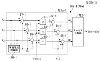
- FIG. 5 is a block diagram showing an example of the control signal generator 78-1 in this embodiment. As shown in FIG. 5, the control signal generator 78-1 includes a duty calculator 781-1 and a carrier comparator 782-1.
- the duty calculator 781-1 outputs a first duty (du1, dv1, dw1), which is a value normalized by the first DC voltage Vdc1s, based on the voltage V u1 , voltage V v1 , and voltage V w1 .
- the duty calculator 781-1 generates the first duty (du1, dv1, dw1), for example, according to the following equation (5).
- the duty calculation unit 781-1 includes a multiplier 81-1, an adder 82-1, a multiplier 83-1, an adder 84-1, a multiplier 85-1, and an adder 86-1.
- the multiplier 81-1 multiplies the voltage Vu1 by (1/Vdc1s) and outputs the multiplication result to the adder 82-1.
- the adder 82-1 adds the constant "0.5" to the output value of the multiplier 81-1, and outputs the result as the first duty du1 to the carrier comparison section 782-1.
- the multiplier 83-1 multiplies the voltage Vv1 by (1/ Vdc1s ) and outputs the multiplication result to the adder 84-1.
- the adder 84-1 adds the constant "0.5" to the output value of the multiplier 83-1 and outputs the result as the first duty dv1 to the carrier comparison section 782-1.
- the multiplier 85-1 multiplies the voltage Vw1 by (1/ Vdc1s ) and outputs the multiplication result to the adder 86-1.
- the adder 86-1 adds the constant "0.5" to the output value of the multiplier 85-1 and outputs the result as the first duty dw1 to the carrier comparison section 782-1.
- the carrier comparison section 782-1 outputs control signals GS11 to GS16 for the inverter 5-1 based on the first duty (du1, dv1, dw1). Now, referring to FIG. 6, the processing of carrier comparison section 782-1 will be described.
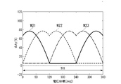
- FIG. 6 is a diagram showing an example of processing of the carrier comparison section 782-1 in this embodiment.
- waveforms W1 to W3 represent waveforms of the first duty (du1, dv1, dw1).
- a waveform W4 represents the waveform of the triangular carrier wave CA whose crest level is "1" and whose trough level is "0".
- Waveforms W5 to W10 indicate waveforms of the control signal GS11, the control signal GS13, the control signal GS15, the control signal GS12, the control signal GS14, and the control signal GS16 in order.
- the carrier comparison unit 782-1 compares the first duty (du1, dv1, dw1) of the waveforms W1 to W3 with the carrier wave CA of the waveform W4. is high, the control signals (GS11, GS13, GS15) corresponding to the switching elements (51-1, 53-1, 55-1) on the high potential side of the inverter 5-1 are turned on (the value is "1"). ). Further, in each phase, when the first duty is low, the carrier comparison unit 782-1 controls the switching elements (51-1, 53-1, 55-1) on the high potential side of the inverter 5-1. The signals (GS11, GS13, GS15) are turned off (the value is "0").
- the carrier comparison unit 782-1 compares the first duty (du1, dv1, dw1) of the waveforms W1 to W3 with the carrier wave CA of the waveform W4, and if the first duty is low in each phase,
- the control signals (GS12, GS14, GS16) corresponding to the switching elements (52-1, 54-1, 56-1) on the low potential side of the inverter 5-1 are turned on (the value is "1").
- the carrier comparison unit 782-1 controls the switching elements (52-1, 54-1, 56-1) on the high potential side of the inverter 5-1.
- the signals (GS12, GS14, GS18) are turned off (the value is "0").
- the carrier comparison unit 782-1 By such processing of the carrier comparison unit 782-1, if any one phase (X phase) among the phases is set to the first duty dx1, the control signal on the high potential side in the period Tc of the carrier wave CA is The rate at which the switching element is turned on is dx1, and the control signal on the low potential side turns the switching element on is (1-dx1). Therefore, the X-phase potential of the inverter 5-1 is the first DC voltage Vdc1 when the high potential side is ON, and the X-phase potential of the inverter 5-1 is "0" (when the low potential side is ON). GND). Therefore, the X-phase output voltage Vx1_PWM is expressed by the following equation (6).
- the X-phase duty is represented by the following formula (7) from the above formula (5).
- the inverter 5-1 can output the voltage according to the command value.
- control unit 7-2 includes a current command calculator 70-2, a subtractor 71-2, a current controller 72-2, a subtractor 73-2, and a current controller. 74-2, a coordinate converter 75-2, a MIN selector 76-2, a coordinate converter 77-2, and a control signal generator 78-2.
- the current command calculator 70-2 generates a d-axis current command value Id_target2 and a q-axis current command value Iq_target2 of the second system from the command value (Ts2) of the rotating machine 10.
- Current command calculator 70-2 has the same configuration as current command calculator 70-1.
- the coordinate converter 75-2 converts the current value I us2 , the current value I vs2 , and the current value I ws2 detected by the current detection unit 6-2 to the current I d2 on the two rotating axes based on the rotational position ⁇ 2 . and current I q2 .
- the coordinate converter 75-2 has the same configuration as the coordinate converter 75-1.
- the MIN selection unit 76-2 compares the first DC voltage Vdc1s and the second DC voltage Vdc2s, and outputs the lower one (the one with the smaller value) as the DC voltage minimum value Vdc_min.
- the MIN selection section 76-2 has the same configuration as the MIN selection section 76-1.
- the subtractor 71-2 subtracts the current Id2 on the rotating two axes from the d-axis current command value Id_target2 , and outputs the result to the current controller 72-2.
- Current Id2 is output from coordinate converter 75-2 .
- the subtractor 73-2 subtracts the current Iq2 on the rotating two axes from the q-axis current command value Iq_target2, and outputs the result to the current controller 74-2.
- Current Iq2 is output from coordinate converter 75-2 .
- the current controller 72-2 performs proportional and integral control on the output value of the subtractor 71-2 so that the output value of the subtractor 71-2 becomes "0" (zero). output the voltage Vd2 above. Since the configuration of the current controller 72-2 is the same as that of the current controller 72-1 described above, the description thereof will be omitted here.
- the current controller 74-2 performs proportional and integral control on the output value of the subtractor 73-2 so that the output value of the subtractor 73-2 becomes "0" (zero). output the voltage V q2 above. Since the configuration of the current controller 74-2 is the same as that of the current controller 74-1 described above, the description thereof will be omitted here.
- the coordinate converter 77-2 converts voltage Vd2 and voltage Vq2, which are voltage commands on the two rotating axes, to voltage Vu2 and voltage Vq2 , which are voltage commands on the three - phase axes, based on the rotational position ⁇ 2.
- V v2 , and voltage V w2 Since the configuration of the coordinate converter 77-2 is the same as that of the coordinate converter 77-1 described above, the description thereof is omitted here.
- the control signal generator 78-2 generates a control signal for the inverter 5-2 based on the second DC voltage Vdc2s and the voltage V u2 , the voltage V v2 , and the voltage V w2 which are the voltage command values on the three-phase axis.
- GS21 to control signal GS26 are output. Since the configuration of the control signal generator 78-2 is the same as that of the control signal generator 78-1 described above, its description is omitted here.
- the current controller 72-1 and the current controller 74-1 select the output V d1 and the output V q1 , which are voltage commands, from the output of the MIN selection unit 76-1.
- the limit is based on a certain DC voltage minimum value Vdc_min.
- the first voltage command vector V1 * generated by the output Vd1 and the output Vq1 is as shown in FIG. , the circle CR2 (size within
- is the second DC voltage Vdc2 (
- Vdc2).
- the circle CR1 indicates a circle whose size is
- the current controller 72-2 and the current controller 74-2 output V d2 and V q2 , which are voltage commands, to the output of the MIN selection unit 76-2. is limited based on the DC voltage minimum value Vdc_min.
- the second voltage command vector V2 * generated by the output Vd2 and the output Vq2 is as shown in FIG. , to the circle CR4, whose size is within
- is the second DC voltage Vdc2 (
- Vdc2).
- the circle CR3 indicates a circle whose size is
- the rotating machine control device 1 increases the rotation speed of the rotating machine 10 and reaches the voltage saturation region, as shown in FIG. Even if it is, the mismatch between systems can be reduced.
- FIG. 9 is a diagram showing the relationship between the number of revolutions and the q-axis current in this embodiment.
- the vertical axis indicates the q-axis current and the number of revolutions
- the horizontal axis indicates time.
- Waveforms W11 and W12 indicate the q -axis current Iq2 of the second system and the q-axis current Iq1 of the first system in this embodiment.
- a waveform W13 indicates the q -axis current Iq1 of the first system in the prior art for comparison.
- a waveform W14 indicates changes in the rotational speed of the rotary machine 10.
- a region RG1 indicates a voltage saturation region.
- the q-axis current Iq1 and the q-axis current Iq2 are limited by the first DC voltage Vdc1 and the second DC voltage Vdc2 , respectively.
- Vdc1 and the second DC voltage Vdc2 are limited by the first DC voltage Vdc1 and the second DC voltage Vdc2 , respectively.
- each of the q-axis current I q1 and the q-axis current I q2 is It decreases with respect to the target q-axis current Iq_target.
- a region RG1 in which the q-axis current Iq1 and the q-axis current Iq2 decrease with respect to the target q-axis current Iq_target is called a voltage saturation region.
- the q-axis current I q1 (waveform W13) is higher than the q-axis current I q2 (waveform W11) in the voltage saturation region. Become. Therefore, in the prior art, it was difficult to equally control the q-axis current Iq1 and the q-axis current Iq2 .
- the voltage command can be made substantially equal (V d1 ⁇ V d2 and V q1 ⁇ V q2 ) even in the voltage saturation region (region RG1), and the q-axis current I q1 and the q-axis current I q2 are substantially can be controlled equally (waveform W11 and waveform W12).
- the rotating machine control device 1 can reduce mismatch between systems (difference in current supplied to the rotating machine 10).
- control signal generator 78-1 of the first system normalizes the voltage command values (V u1 , V v1 , V w1 ) on the three-phase axes with the first DC voltage Vdc1.
- the control signal generator 78-2 of the second system normalizes the voltage command values (V u2 , V v2 , V w2 ) on the three-phase axis with the second DC voltage Vdc2.
- the control unit 7-1 limits the voltage command values (V u1 , V v1 , V w1 ) on the three-phase axis by the DC voltage minimum value Vdc_min. Therefore, normally, the rotating machine 10 can be controlled in a steady state even when normalized by the DC voltage minimum value Vdc_min. However, in a transient state (for example, when there is a sudden change in the q-axis current command value Iq_target1 or a sudden change in the rotation speed), when the voltage command value of the own system is normalized by the DC voltage minimum value Vdc_min, the desired Cannot output voltage.
- Vu1_PWM, Vv1_PWM, Vw1_PWM in this case can be expressed in the following equation (10) by referring to the above equations (6) to (8).
- the three-phase output voltages (Vu1_PWM, Vv1_PWM, Vw1_PWM) are (Vdc1/Vdc_min) times the original voltage command, and the voltage an error occurs.
- This voltage error is absorbed by the current controllers 72-1 and 72-2, so in a steady state, the original voltage command value is multiplied by (Vdc_min/Vdc1).
- the voltage command values (V u1 ', V v1 ', V w1 ') on the three-phase axis are given by Equation (11) below.
- the rotating machine control device 1 can achieve desired transient characteristics by standardizing the voltage command value of the own system with the own system DC voltage.
- the rotating machine control device 1 includes the inverter 5-1 (first inverter), the inverter 5-2 (second inverter), and the control section 7-1 (first control section). and a control unit 7-2 (second control unit).
- the inverter 5-1 applies an AC voltage to the three-phase windings (u1, v1, w1) of the first system based on the first DC voltage Vdc1 output by the DC power supply 3-1 of the first system.
- the inverter 5-2 applies an AC voltage to the three-phase windings (u2, v2, w2) of the second system based on the second DC voltage Vdc2 output by the DC power supply 3-2 of the second system.
- the control unit 7-1 generates a command value for the inverter 5-1 based on the command value (Ts1) for the rotary machine 10, the first DC voltage Vdc1 and the second DC voltage Vdc2.
- the control unit 7-2 generates a command value for the inverter 5-2 based on the command value (Ts1) for the rotary machine 10, the first DC voltage Vdc1 and the second DC voltage Vdc2.
- Each of the control unit 7-1 and the control unit 7-2 controls the DC voltage of the own system (eg, the first DC voltage Vdc1) to the DC voltage of the other system (eg, the second DC voltage Vdc2).
- a value obtained by normalizing the own system voltage command by the own system DC voltage (eg, the first DC voltage Vdc1) (see, for example, formula (5) and formula (7)) to the inverter 5 of the own system (for example, the inverter 5- 1) is generated as a command value.
- the rotating machine control device 1 uses the DC voltage minimum value Vdc_min, which is one of the smaller values of the first DC voltage Vdc1 and the second DC voltage Vdc2, to Since the self-system voltage command value to be applied to is limited, mismatch between systems (difference in current supplied to rotating machine 10) can be reduced.
- Vdc_min is one of the smaller values of the first DC voltage Vdc1 and the second DC voltage Vdc2
- the rotating machine control device 1 normalizes the own system voltage command by the own system DC voltage (first duty, second duty) to the inverters 5 of the first system and the second system ( 5-1 and 5-2), the transient characteristics can be improved.
- control unit 7-1 has a first CPU
- control unit 7-2 has a second CPU.
- the rotating machine control device 1 can control the rotating machine 10 with the other system even if one of the systems fails, for example, by executing processing using two independent CPUs. can be continued.
- the control unit 7 controls the DC voltage of the own system (for example, the first DC voltage Vdc1) to the DC voltage of another system (for example, the second DC voltage Vdc2).
- the rotary machine control device 1 can adjust the voltage commands on the dq axes to match between the systems.
- the control unit 7 controls the DC voltage of the own system (for example, the first DC voltage Vdc1) to the DC voltage of another system (for example, the second DC voltage Vdc2).
- the rotating machine control device 1 can adjust the magnitudes of the voltage command vectors on the stationary coordinate axes to match between the systems.
- FIG. 10 is a block diagram showing an example of a rotary machine control device 1a according to the second embodiment.
- the rotating machine control device 1a includes a position detector 2, a DC power supply 3-1, a DC power supply 3-2, a capacitor 4-1, a capacitor 4-2, an inverter 5-1, and a , an inverter 5-2, a current detection unit 6-1, a current detection unit 6-2, a control unit 7a-1, and a control unit 7a-2.
- the same reference numerals are assigned to the same configurations as those of the first embodiment shown in FIG. 1, and the description thereof will be omitted.
- the rotary machine control device 1a includes control units 7a (7a-1, 7a-2) instead of the control units 7 (7-1, 7-2), which is different from the first embodiment. It differs from the rotating machine control device 1 .
- the first system has a wiring resistance (Rp1) in the DC section flowing from the DC power supply 3-1 to the inverter 5-1, and a voltage drop occurs due to the wiring resistance (Rp1). is defined as a first DC voltage Vdc1_real.
- the second system has a wiring resistance (Rp2) in the DC section that flows from the DC power supply 3-2 to the inverter 5-2, and the true DC voltage resulting from the voltage drop due to the wiring resistance (Rp2) is 2 DC voltage Vdc2_real.
- the control unit 7a-1 (an example of the first control unit) includes, for example, a CPU, and controls the rotating machine 10 by the first system.
- the control unit 7a-1 controls the current command values (Id_target1, Iq_target1), the rotational position ⁇ 1 detected by the position detection unit 2 , the current value Ius1 detected by the current detection unit 6-1, the current value Ivs1 , and the control signal GS11 to control signal GS16 (first control signal ).
- the control unit 7a-2 (an example of the second control unit) includes, for example, a CPU, and controls the rotating machine 10 by the second system.
- the control unit 7a-2 controls the current command values (Id_target2, Iq_target2), the rotational position ⁇ 1 detected by the position detection unit 2 , the current value I us2 detected by the current detection unit 6-2, the current value I vs2 , and the control signal GS21 to control signal GS26 (second control signal ).
- FIG. 11 is a block diagram showing an example of the two-system control units 7a of the rotating machine control device 1a according to the present embodiment.
- the control unit 7a-1 includes a current command calculator 70-1, a subtractor 71-1, a current controller 72-1, a subtractor 73-1, a current controller 74- 1, a coordinate converter 75-1, a MIN selection unit 76-1, a coordinate converter 77-1, a control signal generator 78-1, a self-system battery current calculation unit 61-1, and another system battery It includes a current calculator 62-1 and a voltage deviation calculator 63-1.
- MIN selection unit 76-1 and voltage deviation calculation unit 63-1 are included in voltage minimum value calculation unit 60-1.
- Own system battery current calculation unit 61-1 calculates own system three-phase current values (current value I us1 , current value I vs1 , and current value I ws1 ) and the first duty (du1, dv1 , dw1), the current Idc1 of the own system is calculated.
- the self-system current I dc1 (self-system DC part current) here is the DC part current that flows into the inverter 5-1 and is the first system DC part current.
- the self-system battery current calculator 61-1 calculates the current Idc1 of the self-system using, for example, the following equation (12).
- the other-system battery current calculation unit 62-1 provides a current Idc1 of the own system, a first DC voltage Vdc1s that is the detected value of the DC voltage of the own system, and a second DC voltage that is the detected value of the DC voltage of the other system.
- the current Idc2 of the other system is calculated based on Vdc2s.
- the other system current I dc2 (another system DC part current) is a DC part current that flows into the inverter 5-2, and is a second system DC part current.
- the other system battery current calculator 62-1 calculates the current Idc2 of the other system using, for example, the following equation (13).
- the voltage deviation calculation unit 63-1 calculates a value based on the own-system current Idc1 output by the own-system battery current calculation unit 61-1 and the other-system current Idc2 output by the other-system battery current calculation unit 62-1 . to calculate the voltage deviation ⁇ Va of the first system.
- the voltage deviation calculator 63-1 calculates the voltage deviation ⁇ V a of the first system using, for example, the following equation (14).
- the voltage minimum value calculator 60-1 includes a MIN selector 76-1 and a voltage deviation calculator 63-1. Based on the DC voltage minimum value Vdc_min output by the MIN selection unit 76-1 and the voltage deviation ⁇ V a of the first system calculated by the voltage minimum value calculation unit 60-1, the voltage minimum value calculation unit 60-1 A new DC voltage minimum value Vdc_min2 is generated, and the generated DC voltage minimum value Vdc_min2 is output.
- DC voltage minimum value Vdc_min2 is a correction value of DC voltage minimum value Vdc_min in consideration of voltage deviation ⁇ Va.
- Voltage minimum value calculation section 60-1 calculates DC voltage minimum value Vdc_min2 using, for example, the following equation (15).
- the DC voltage minimum value Vdc_min2 output by the voltage minimum value calculation unit 60-1 is supplied to the subtractors 71-1 and 73-1 instead of the DC voltage minimum value Vdc_min. Subsequent processing by the control unit 7a-1 is the same as that of the control unit 7-1 of the first embodiment, so description thereof will be omitted here.
- control unit 7a-2 includes a current command calculator 70-2, a subtractor 71-2, a current controller 72-2, a subtractor 73-2, a current controller 74-2, a coordinate conversion device 75-2, MIN selection unit 76-2, coordinate converter 77-2, control signal generator 78-2, own system battery current calculation unit 61-2, other system battery current calculation unit 62- 2 and a voltage deviation calculator 63-2.
- MIN selection unit 76-2 and voltage deviation calculation unit 63-2 are included in voltage minimum value calculation unit 60-2.
- Own system battery current calculation unit 61-2 calculates own system three-phase current values (current value I us2 , current value I vs2 , and current value I ws2 ) and the second duty (du2, dv2 , dw2), the current Idc2 of the own system is calculated.
- the self-system current I dc2 (self-system DC part current) here is the DC part current that flows into the inverter 5-2 and is the second system DC part current.
- the self-system battery current calculator 61-2 calculates the current Idc2 of the self-system using, for example, the following equation (16).
- the other-system battery current calculation unit 62-2 generates a current Idc2 of the own system, a second DC voltage Vdc2s that is the detected value of the DC voltage of the own system, and a first DC voltage that is the detected value of the DC voltage of the other system.
- the current Idc1 of the other system is calculated based on Vdc1s.
- the other system current I dc1 (another system DC part current) is the DC part current flowing into the inverter 5-1 and is the first system DC part current.
- the other system battery current calculator 62-1 calculates the current Idc1 of the other system using, for example, the following equation (17).
- the voltage deviation calculation unit 63-2 calculates a value based on the own system current Idc2 output by the own system battery current calculation unit 61-2 and the other system current Idc1 output by the other system battery current calculation unit 62-2 . to calculate the voltage deviation ⁇ Vb of the second system.
- the voltage deviation calculator 63-2 calculates the voltage deviation ⁇ V b of the second system using, for example, the following equation (18).
- the voltage minimum value calculator 60-2 includes a MIN selector 76-2 and a voltage deviation calculator 63-2. Based on the DC voltage minimum value Vdc_min output by the MIN selection unit 76-2 and the voltage deviation ⁇ Vb of the second system calculated by the voltage minimum value calculation unit 60-2, the voltage minimum value calculation unit 60-2 A new DC voltage minimum value Vdc_min2 is generated, and the generated DC voltage minimum value Vdc_min2 is output.
- DC voltage minimum value Vdc_min2 is a correction value of DC voltage minimum value Vdc_min in consideration of voltage deviation ⁇ Vb.
- Voltage minimum value calculation section 60-2 calculates DC voltage minimum value Vdc_min2 using, for example, the following equation (19).
- the DC voltage minimum value Vdc_min2 output by the voltage minimum value calculation unit 60-2 is supplied to the subtractors 71-2 and 73-2 instead of the DC voltage minimum value Vdc_min. Subsequent processing by the controller 7a-2 is similar to that of the controller 7-2 of the first embodiment.
- the inverters 5-1 and 5-2 since there is a wiring resistance Rp , a deviation occurs between the detected voltage Vdc1s of the own system and the true input voltage Vdc1_real. Further, since the wiring resistance Rp exists in the inverter 5-2, a deviation occurs between the detected voltage Vdc2s of the own system and the true input voltage Vdc2_real. Therefore, in order to match the current of the first system and the current of the two systems supplied to the rotating machine 10, the inverters 5-1 and 5-2 must have the true input voltage Vdc1_real and the true input voltage Vdc2_real. It is necessary to apply a voltage based on the voltage on the smaller side of .
- the rotary machine control device 1a corrects this error using the voltage deviation calculator 63-1 and the voltage deviation calculator 63-2.
- the rotating machine control device 1a performs control so that the inverters 5-1 and 5-2 supply the same power to the rotating machine 10, so the following equation (20) holds.
- the MIN selection unit 76-1 selects the voltage Vdc2s as the DC voltage minimum value Vdc_min. 1 is output.
- the voltage minimum value calculation unit 60-1 uses the voltage deviation ⁇ V a shown by Equation (14) to correct the DC voltage minimum value Vdc_min.
- the voltage (input voltage Vdc1_real) applied to the inverter 5-1 is represented by the following equation (24).
- Equation (24) The right side of Equation (24) is the same as the input voltage Vdc2_real indicated by Equation (21) above. Therefore, in the rotary machine control device 1a according to the present embodiment, the voltage applied to the inverter 5-1 (input voltage Vdc1_real) matches the voltage applied to the inverter 5-2 (input voltage Vdc2_real).
- the current Idc1 of the first system is the current of the second system according to the above equation (13). greater than I dc2 (I dc1 >I dc2 ).
- the input voltage Vdc1_real given by the above equation (21) is output to the inverter 5-1.
- MIN selection unit 76-2 selects voltage Vdc1s as DC voltage minimum value Vdc_min. 2 is output.
- the voltage applied to the inverter 5-1 (input voltage Vdc1_real ) and the voltage applied to the inverter 5-2 (input voltage Vdc2_real) are do not match. Therefore, the current flowing through the three-phase windings (u1, v1, w1) of the first system does not match the current flowing through the three-phase windings (u2, v2, w2) of the second system, For example, noise may occur in the rotating machine 10 .
- the voltage minimum value calculation unit 60-2 uses the voltage deviation ⁇ Vb shown by Equation (14) to correct the DC voltage minimum value Vdc_min .
- the voltage (input voltage Vdc2_real) applied to the inverter 5-2 is represented by the following equation (27).
- Equation (27) The right side of Equation (27) is the same as the input voltage Vdc1_real indicated by Equation (21) above. Therefore, in the rotary machine control device 1a according to the present embodiment, the voltage applied to the inverter 5-1 (input voltage Vdc1_real) matches the voltage applied to the inverter 5-2 (input voltage Vdc2_real).
- the control unit 7a controls the voltage deviation ( ⁇ V a , ⁇ V b ) to , limit the own system voltage command.
- the voltage deviations ( ⁇ V a , ⁇ V b ) are the DC current (current I dc1 ) of the first system, which is the DC current flowing into the inverter 5-1, and the DC current flowing into the inverter 5-2.
- the value obtained by subtracting the DC part current of the own system from the DC part current of the other system of the DC part current (current I dc2 ) of the second system is the resistance of the wiring through which the DC part current of the own system flows It is a value obtained by multiplying the wiring resistance (R p ) (see equations (14) and (18)).
- the rotating machine control device 1a according to the present embodiment can match the voltages output from the inverters 5-1 and 5-2 even when the wiring resistance Rp of the inverter 5 exists, as described above. It is possible to reduce the mismatch between systems.
- the currents supplied to the three-phase windings (u1, v1, w1) of the first system and the three-phase windings (u2, v2, w2) of the second system match. Therefore, for example, noise generated from the rotating machine 10 can be reduced.
- the controller 7a calculates the DC part current of the other system based on the DC voltage of the other system.
- the rotating machine control device 1a according to the present embodiment calculates the DC part current of the other system, it is not necessary to detect the DC part current of the other system. Therefore, the rotating machine control device 1a according to the present embodiment can reduce the number of detection units such as sensors, simplify the configuration, and realize cost reduction.
- control unit 7a calculates the DC part current of the other system based on the DC voltage of the own system, the DC voltage of the other system, and the DC current of the own system (equation (13) and (17)).
- the rotating machine control device 1a according to the present embodiment can easily calculate the DC part current of the other system using a simple method.
- the rotating machine control device 1a includes current detection units 6 (6-1, 6-2) that detect currents flowing through the three-phase windings of each system.
- the control unit 7a calculates the direct current of its own system based on the current flowing through the 3-phase winding of its own system detected by the current detection unit 6 (see equations (12) and (16)).
- the rotating machine control device 1a according to the present embodiment can easily calculate the DC part current of its own system by a simple method.
- the minimum voltage value calculator 60-1 of the first system calculates the battery current I dc2 of the other system using the above-described formula (13) or formula (14) in the other system. The calculated value may be received from another system and used.
- the second system voltage minimum value calculation unit 60-2 calculates the battery current I dc1 of the other system, the value calculated using the above-described formula (12) or formula (17) in the other system, It may be received from the system and used.
- the rotating machine control device 1b includes control signal generators 78a (78a-1, 78a-2) instead of the control signal generators 78 (78-1, 78-2), and other configurations are , is the same as the rotating machine control device 1 of the first embodiment.
- FIG. 12 is a block diagram showing an example of the control signal generator 78a-1 of the first system in this embodiment.
- the control signal generator 78a-1 includes a duty calculator 781a-1 and a carrier comparator 782-1. 12, the same components as in FIG. 5 described above are denoted by the same reference numerals, and description thereof will be omitted.
- the control signal generator 78a-1 generates a control signal for the inverter 5-1 based on the first DC voltage Vdc1s and the voltage V u1 , voltage V v1 , and voltage V w1 which are voltage command values on the three-phase axis.
- GS11 to control signal GS16 are output.
- the rotating machine control device 1b includes a control section 7b-1 of the first system, and the control section 7b-1 includes a control signal generator 78a-1.
- the duty calculator 781a-1 outputs a first duty (du1, dv1, dw1), which is a value normalized by the first DC voltage Vdc1s, based on the voltage V u1 , the voltage V v1 , and the voltage V w1 .
- the duty calculation unit 781a-1 includes a zero-phase voltage calculation unit 80-1, a multiplier 81-1, an adder 82-1, a multiplier 83-1, an adder 84-1, and a multiplier 85- 1, an adder 86-1, a subtractor 87-1, a subtractor 88-1, and a subtractor 89-1.
- the duty calculation unit 781a-1 is the first in that a zero-phase voltage calculation unit 80-1, a subtractor 87-1, a subtractor 88-1, and a subtractor 89-1 are added. is different from the duty calculation section 781-1 of the embodiment.
- the zero-phase voltage calculator 80-1 calculates the zero-phase voltage V 0a based on the voltage command values of the voltage V u1 , the voltage V v1 , and the voltage V w1 and the detected voltage Vdc1s of the own system.
- the zero-phase voltage calculator 80-1 calculates the zero-phase voltage V0a using, for example, the following equation (28). Note that the zero-phase voltage calculation unit 80-1 determines that the minimum self-system voltage command (voltage V u1 , voltage V v1 , and voltage V w1 ) is a predetermined lower limit value (for example, , 0V), the zero-phase voltage V0a of the own system is calculated.
- the minimum voltage V min is the minimum value of the voltage V u1 , the voltage V v1 , and the voltage V w1 at the time of calculating the zero-phase voltage V 0a .
- Zero-phase voltage calculation unit 80-1 determines that the minimum (minimum voltage V min ) of self-system voltage commands (voltage V u1 , voltage V v1 , and voltage V w1 ) is a predetermined voltage based on self-system DC voltage Vdc1s.
- the zero-phase voltage V0a of the own system is obtained by adding half the DC voltage Vdc1s of the own system (Vdc1s/2) to the minimum voltage Vmin so as to match the lower limit value (for example, 0V). calculate.
- the subtractor 87-1 outputs a value obtained by subtracting the zero-phase voltage V0a from the voltage Vu1 , which is the voltage command value, to the multiplier 81-1.
- the subtractor 88-1 outputs a value obtained by subtracting the zero-phase voltage V0a from the voltage Vv1 , which is the voltage command value, to the multiplier 83-1.
- the subtractor 89-1 outputs a value obtained by subtracting the zero-phase voltage V0a from the voltage Vw1 , which is the voltage command value, to the multiplier 85-1.
- the duty calculator 781a-1 calculates the first duty (du1, dv1, dw1) using the following equation (29).
- FIG. 13 is a block diagram showing an example of the second-system control signal generator 78a-1 in this embodiment.
- the control signal generator 78a-2 includes a duty calculator 781a-2 and a carrier comparator 782-2.
- the control signal generator 78a-2 generates a control signal for the inverter 5-2 based on the second DC voltage Vdc2s and the voltage command values V u2 , V v2 , and V w2 on the three-phase axis.
- GS21 to control signal GS26 are output.
- the rotating machine control device 1b includes a control unit 7b-2 of the second system, and the control unit 7b-2 includes a control signal generator 78a-2.
- the duty calculator 781a-2 outputs a second duty (du2, dv2, dw2), which is a value normalized by the second DC voltage Vdc2s, based on the voltage V u2 , the voltage V v2 , and the voltage V w2 .
- the duty calculation unit 781a-2 includes a zero-phase voltage calculation unit 80-2, a multiplier 81-2, an adder 82-2, a multiplier 83-2, an adder 84-2, and a multiplier 85- 2, an adder 86-2, a subtractor 87-2, a subtractor 88-2, and a subtractor 89-2.
- the duty calculation unit 781a-2 is the first in that a zero-phase voltage calculation unit 80-2, a subtractor 87-2, a subtractor 88-2, and a subtractor 89-2 are added. is different from the duty calculation section 781-2 of the embodiment.
- the zero-phase voltage calculator 80-2 calculates the zero-phase voltage V 0b based on the voltage command values of the voltage V u2 , the voltage V v2 , and the voltage V w2 and the detected voltage Vdc2s of the own system.
- the zero-phase voltage calculator 80-2 calculates the zero-phase voltage V0a using, for example, the following equation (30). Note that the zero-phase voltage calculation unit 80-1 determines that the minimum self-system voltage command (voltage V u2 , voltage V v2 , and voltage V w2 ) is a predetermined lower limit value (for example, , 0V), the zero-phase voltage V0b of the own system is calculated.
- the minimum voltage V min is the minimum value of the voltage V u2 , the voltage V v2 , and the voltage V w2 at the time of calculating the zero-phase voltage V 0b .
- Zero-phase voltage calculation unit 80-2 determines that the minimum (minimum voltage V min ) of self-system voltage commands (voltage V u2 , voltage V v2 , and voltage V w2 ) is a predetermined voltage based on self-system DC voltage Vdc2s. To match the lower limit value (for example, 0 V), the zero-phase voltage V0b of the own system is obtained by adding half the value (Vdc2s/2) of the DC voltage Vdc2s of the own system to the minimum voltage Vmin. calculate.
- the subtractor 87-2 outputs a value obtained by subtracting the zero-phase voltage V0b from the voltage Vu2 , which is the voltage command value, to the multiplier 81-2.
- the subtractor 88-2 outputs a value obtained by subtracting the zero-phase voltage V0b from the voltage Vv2 , which is the voltage command value, to the multiplier 83-2.
- the subtractor 89-2 outputs a value obtained by subtracting the zero-phase voltage V0b from the voltage Vw2, which is the voltage command value, to the multiplier 85-2.
- the duty calculator 781a-2 calculates the second duty (du2, dv2, dw2) using the following equation (31).
- the duty calculation section 781a-1 and the duty calculation section 781a-2 use the detected voltages (Vdc1s, Vdc2s) of the own system, and according to the equations (28) and (30), , zero-phase voltages (V 0a , V 0b ) are calculated, and the zero-phase voltages are subtracted from the voltage command value, thereby shifting the duty value downward within a range in which voltage saturation does not occur.
- the control unit 7b-1 of the first system and the control unit 7b-2 of the second system have the same configuration. Description will be made by omitting "-2", subscripts "1" and “2", and [a] and "b" in the zero-phase voltage.
- the zero -phase voltage V0 is expressed by the following equation (32).
- the new voltage command value V u ' is represented by the following equation (34).
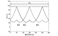
- the duty du' is expressed by the following equation (36). Considering the duties of other phases in the same way, the duty of each phase has a waveform as shown in FIG.
- FIG. 14 is a diagram showing duty waveforms of respective phases when the detection voltages of other systems are used in this embodiment.
- the horizontal axis of the graph indicates the voltage phase
- the vertical axis indicates the duty.
- a waveform W21, a waveform W22, and a waveform W23 respectively indicate the duty waveform of the U phase, the duty waveform of the V phase, and the duty waveform of the W phase.
- a period TR1 indicates a period in which the three phases are always switched.
- the control unit 7b when the value of the other system is used as the detection voltage Vdc', the control unit 7b always performs control to perform three-phase switching.
- the minimum duty of the three phases is always “0", so the switching element on the upper arm side (high potential side) is always on in that phase. is.
- FIG. 15 is a diagram showing the duty waveform of each phase when using the detected voltage of its own system in this embodiment.
- the horizontal axis of the graph indicates the voltage phase
- the vertical axis indicates the duty.
- a waveform W24, a waveform W25, and a waveform W26 respectively indicate the duty waveform of the U phase, the duty waveform of the V phase, and the duty waveform of the W phase.
- a period TR2 indicates a period in which two phases are always switched.
- the control unit 7b performs control so that two-phase switching is always performed. That is, the rotating machine control device 1b according to the present embodiment always performs two-phase switching by using the detected voltage Vdc of its own system when calculating the zero -phase voltage V0. Therefore, the rotating machine control device 1b according to the present embodiment can reduce the switching loss and improve the current detection accuracy as compared with the case of using the detected voltage of the other system.
- the control unit 7b calculates the zero-phase voltages (V 0a , V 0b ) of the own system based on the DC voltage of the own system, and is corrected based on the zero-phase voltages (V 0a , V 0b ) of the own system.
- the rotating machine control device 1b can perform two-phase modulation (constant two-phase switching), and can reduce the influence of noise on current detection.
- control unit 7b calculates the zero-phase voltage of the own system so that the minimum of the own system voltage command matches a predetermined lower limit value based on the DC voltage of the own system.
- the rotating machine control device 1b according to the present embodiment can appropriately shift the value of the duty downward within a range in which voltage saturation does not occur.
- the rotating machine control device 1c includes control signal generators 78b (78b-1, 78b-2) instead of the control signal generators 78a (78a-1, 78a-2), and other configurations are , is the same as the rotating machine control device 1a of the second embodiment.
- FIG. 16 is a block diagram showing an example of the control signal generator 78b-1 of the first system in this embodiment.
- the control signal generator 78b-1 includes a duty calculator 781b-1 and a carrier comparator 782-1. 16, the same components as in FIG. 12 described above are denoted by the same reference numerals, and description thereof will be omitted.
- the control signal generator 78b-1 generates a control signal for the inverter 5-1 based on the first DC voltage Vdc1s and voltage V u1 , voltage V v1 , and voltage V w1 which are voltage command values on the three-phase axis.
- GS11 to control signal GS16 are output.
- the rotating machine control device 1c includes a first system control section 7c-1, and the control section 7c-1 includes a control signal generator 78b-1.
- the duty calculator 781b-1 outputs a first duty (du1, dv1, dw1), which is a value normalized by the first DC voltage Vdc1s, based on the voltage V u1 , voltage V v1 , and voltage V w1 .
- the duty calculation unit 781b-1 includes a zero-phase voltage calculation unit 80a-1, a multiplier 81-1, an adder 82-1, a multiplier 83-1, an adder 84-1, and a multiplier 85- 1, an adder 86-1, a subtractor 87-1, a subtractor 88-1, and a subtractor 89-1.
- the duty calculation section 781b-1 differs from the duty calculation section 781a-1 of the third embodiment in that it includes a zero-phase voltage calculation section 80a-1 instead of the zero-phase voltage calculation section 80-1.
- the zero-phase voltage calculation unit 80a-1 calculates the zero-phase voltage V 0a based on the voltage command values of the voltage V u1 , the voltage V v1 , and the voltage V w1 and the detected voltage Vdc1s of the own system.
- the zero-phase voltage calculator 80a-1 calculates the zero-phase voltage V0a using, for example, the following equation (38). Note that the zero-phase voltage calculation unit 80a-1 determines that the maximum self-system voltage command (voltage V u1 , voltage V v1 , and voltage V w1 ) is a predetermined upper limit value (for example, , Vdc1s), the zero-phase voltage V0a of the own system is calculated.
- the maximum voltage V max is the maximum value of the voltage V u1 , the voltage V v1 , and the voltage V w1 at the time of calculating the zero-phase voltage V 0a .
- the zero-phase voltage calculation unit 80a-1 determines that the maximum (maximum voltage V max ) of the self-system voltage commands (voltage V u1 , voltage V v1 , and voltage V w1 ) is a predetermined voltage based on the self-system DC voltage Vdc1s. Subtract half the DC voltage Vdc1s of the own system (Vdc1s/2) from the maximum voltage Vmax so as to match the upper limit value (for example, Vdc1s) to obtain the zero-phase voltage V0a of the own system. calculate.
- FIG. 17 is a block diagram showing an example of the second system control signal generator 78b-1 in this embodiment.
- the control signal generator 78b-2 includes a duty calculator 781b-2 and a carrier comparator 782-2.
- the control signal generator 78b-2 generates a control signal for the inverter 5-2 based on the second DC voltage Vdc2s and the voltage command values V u2 , V v2 , and V w2 on the three-phase axis.
- GS21 to control signal GS26 are output.
- the rotating machine control device 1c includes a control unit 7c-2 of the second system, and the control unit 7c-2 includes a control signal generator 78b-2.
- the duty calculator 781b-2 outputs a second duty (du2, dv2, dw2), which is a value normalized by the second DC voltage Vdc2s, based on the voltage V u2 , the voltage V v2 , and the voltage V w2 .
- the duty calculation unit 781b-2 includes a zero-phase voltage calculation unit 80a-2, a multiplier 81-2, an adder 82-2, a multiplier 83-2, an adder 84-2, and a multiplier 85- 2, an adder 86-2, a subtractor 87-2, a subtractor 88-2, and a subtractor 89-2. Note that the duty calculation section 781b-2 differs from the duty calculation section 781a-2 of the third embodiment in that a zero-phase voltage calculation section 80a-2 is provided instead of the zero-phase voltage calculation section 80-2.
- the zero-phase voltage calculator 80a-2 calculates the zero-phase voltage V 0b based on the voltage command values of the voltage V u2 , the voltage V v2 , and the voltage V w2 and the detected voltage Vdc2s of the own system.
- the zero-phase voltage calculator 80a-2 calculates the zero-phase voltage V0b using, for example, the following equation (39). Note that the zero-phase voltage calculation unit 80a-2 determines that the maximum self-system voltage command (voltage V u2 , voltage V v2 , and voltage V w2 ) is a predetermined upper limit value (for example, , Vdc2s), the zero-phase voltage V0b of the own system is calculated.
- the maximum voltage V max is the maximum value of the voltage V u2 , the voltage V v2 , and the voltage V w2 at the time of calculating the zero-phase voltage V 0b .
- the zero-phase voltage calculator 80a-2 sets the maximum (maximum voltage V max ) of the self-system voltage commands (voltage V u2 , voltage V v2 , and voltage V w2 ) to a predetermined voltage based on the self-system DC voltage Vdc2s. To match the lower limit (for example, Vdc2s), the zero-phase voltage V0b of the own system is added to the maximum voltage Vmax by adding half the DC voltage Vdc2s of the own system (Vdc2s/2). calculate.
- the duty calculation section 781b-1 and the duty calculation section 781b-2 use the detected voltages (Vdc1s, Vdc2s) of the own system, and according to the equations (38) and (39), , zero-phase voltages (V 0a , V 0b ) are calculated, and the zero-phase voltages are subtracted from the voltage command value, thereby shifting the duty value upward within a range in which voltage saturation does not occur.
- the control unit 7c-1 of the first system and the control unit 7c-2 of the second system have the same configuration. Description will be made by omitting "-2", subscripts "1" and “2", and [a] and "b" in the zero-phase voltage.
- the zero -phase voltage V0 is expressed by the following equation (40).
- the new voltage command value V w ' is represented by the following equation (42).
- the duty dw' is expressed by the following equation (44). Considering the duties of other phases in the same way, the duty of each phase has a waveform as shown in FIG.
- FIG. 18 is a diagram showing the duty waveform of each phase when the detection voltage of another system is used in this embodiment.
- the horizontal axis of the graph indicates the voltage phase
- the vertical axis indicates the duty.
- a waveform W31, a waveform W32, and a waveform W33 respectively indicate the duty waveform of the U phase, the duty waveform of the V phase, and the duty waveform of the W phase.
- a period TR3 indicates a period in which three phases are always switched.
- control unit 7c when the value of the other system is used as the detection voltage Vdc', the control unit 7c always performs control to perform three-phase switching.
- the duty dw' is expressed by the following equation (45). Considering the duties of other phases in the same way, the duty of each phase has a waveform as shown in FIG.
- the maximum duty among the three phases is always “1", so in the phase, the switching element on the lower arm side (low potential side) is always on. is.
- FIG. 19 is a diagram showing the duty waveform of each phase when using the detected voltage of its own system in this embodiment.
- the horizontal axis of the graph indicates the voltage phase
- the vertical axis indicates the duty.
- a waveform W34, a waveform W35, and a waveform W36 indicate the duty waveform of the U phase, the duty waveform of the V phase, and the duty waveform of the W phase, respectively.
- a period TR4 indicates a period in which two phases are always switched.
- the control unit 7c performs control so that two-phase switching is always performed. That is, the rotating machine control device 1c according to the present embodiment always performs two-phase switching by using the detected voltage Vdc of its own system when calculating the zero -phase voltage V0. Therefore, the rotating machine control device 1c according to the present embodiment can reduce the switching loss and improve the current detection accuracy as compared with the case where the detection voltage of the other system is used.
- the control unit 7c calculates the self-system zero-phase voltages (V 0a , V 0b ) based on the self-system DC voltage, and is corrected based on the zero-phase voltages (V 0a , V 0b ) of the own system.
- the rotating machine control device 1c can perform two-phase modulation (constant two-phase switching), and can reduce the influence of noise on current detection.
- control unit 7c calculates the zero-phase voltage of the own system so that the maximum of the own system voltage command matches a predetermined upper limit value based on the DC voltage of the own system.
- the rotating machine control device 1c according to the present embodiment can appropriately shift the duty value upward within a range in which voltage saturation does not occur.
- FIG. 20 is a block diagram showing an example of the electric power steering device 100 according to the fifth embodiment.
- the electric power steering device 100 includes a rotary machine 10, a steering wheel 101, a torque sensor 102, a steering shaft 103, wheels 104, a rack and pinion gear 105, and a control device 106.
- the control device 106 includes the rotary machine control device 1 (1a, 1b, 1c) described above.
- a torque sensor 102 detects a steering torque of a driver (not shown).
- the wheels 104 are, for example, wheels to be steered of a vehicle such as an automobile.
- the steering torque applied by the driver to the steering wheel 101 passes through the torsion bar of the torque sensor 102 and the steering shaft 103, and is transmitted to the rack via the rack and pinion gear 105. Thereby, the electric power steering device 100 steers the wheels 104 .
- the rotating machine 10 is driven by the rotating machine control device 1 (1a, 1b, 1c) of the control device 106 and generates an assist force as an output.
- the assist force is transmitted to the steering shaft 103 and reduces the steering torque applied by the driver during steering.
- the control device 106 calculates an assist command for adjusting the assist force based on the driver's steering torque detected by the torque sensor 102 .
- the control device 106 calculates the assist command as a value proportional to the driver's steering torque.
- the control device 106 sets an assist command as a torque command that is a command value for the rotating machine 10 .
- the electric power steering apparatus 100 includes the rotary machine control device 1 (1a, 1b, 1c) described above, the rotary machine 10 for assisting the steering, and the steering torque of the steering.
- a torque sensor 102 is provided.
- the rotary machine control device 1 (1a, 1b, 1c) controls the rotary machine 10 using a steering assist command corresponding to the steering torque detected by the torque sensor 102 as a command value for the rotary machine 10.
- the electric power steering apparatus 100 achieves the same effect as the rotating machine control apparatus 1 (1a, 1b, 1c) described above, and controls the rotating machine 10 in a plurality of systems of DC power supplies (3- 1, 3-2), even if there is a difference in the output DC voltage, the mismatch between systems can be reduced. Further, the electric power steering apparatus 100 according to the present embodiment can obtain an assist torque from the rotating machine 10 according to the steering by the driver, and can stably control the rotating machine 10 by using two current systems. Therefore, an electric power steering device that can be steered comfortably can be realized.
- the present disclosure is not limited to the above-described embodiments, and can be modified without departing from the gist of the present disclosure.
- the control target value is the speed command value of the rotating machine 10
- the control target value is Position command value.
- the current command calculator 70-1 generates current command values (Id_target1, Iq_target1) from the command signal Ts1 of the rotating machine 10, and the current command calculator 70-2 generates
- Id_target1, Iq_target1 current command values from the command signal Ts1 of the rotating machine 10
- Id_target2, Iq_target2 current command values from 10 command signals Ts2
- the present invention is not limited to this.
- the same command signal Ts may be input to the current command calculator 70-1 and the current command calculator 70-2.
- One of the two systems of control units 7 (7a, 7b, 7c) includes a current command calculator 70, and current command values (Id_target, Iq_target) generated by one current command calculator 70 may be used in two control units 7 (7a, 7b, 7c). Further, a third control unit including a current command calculator 70 for generating current command values (Id_target, Iq_target) is provided, and the current command value (Id_target) generated by the current command calculator 70 of the third control unit , Iq_target) may be used in two systems of control units 7 (7a, 7b, 7c).
- the d-axis current command value Id_target1 and the q-axis current command value Iq_target1 may be generated based on the value Vdc_min and the command value for the rotating machine 10 .
- the current command calculator 70-2 may generate the d-axis current command value Id_target2 and the q-axis current command value Iq_target2 based on the DC voltage minimum value Vdc_min and the command value of the rotating machine 10. .
- control units 7-1 (7a-1, 7b-1, 7c-1) of the first system and the control units 7-2 (7a-2, 7b-2) of the second system , 7c-2) and 7c-2) each have a CPU, but the present invention is not limited to this. Even if both the control units 7-1 (7a-1, 7b-1, 7c-1) and the control units 7-2 (7a-2, 7b-2, 7c-2) are controlled by one CPU good. In this case, one CPU takes in the first DC voltage Vdc1s and the second DC voltage Vdc2s, and -2, 7b-2, 7c-2).
- each configuration included in the rotating machine control device 1 (1a, 1b, 1c) described above has a computer system therein. Then, a program for realizing the function of each configuration provided in the rotating machine control device 1 (1a, 1b, 1c) described above is recorded in a computer-readable recording medium, and the program recorded in this recording medium is executed by a computer.
- the processing in each configuration included in the rotating machine control device 1 (1a, 1b, 1c) described above may be performed by loading the system and executing it.
- "loading and executing the program recorded on the recording medium into the computer system” includes installing the program in the computer system.
- the "computer system” here includes hardware such as an OS and peripheral devices.
- the "computer system” may include a plurality of computer devices connected via a network including communication lines such as the Internet, WAN, LAN, and dedicated lines.
- the term "computer-readable recording medium” refers to portable media such as flexible discs, magneto-optical discs, ROMs and CD-ROMs, and storage devices such as hard discs incorporated in computer systems.
- the recording medium storing the program may be a non-transitory recording medium such as a CD-ROM.
- Recording media also include internal or external recording media that can be accessed from the distribution server in order to distribute the program.
- a configuration in which a program is divided into a plurality of programs and downloaded at different timings and then merged in each configuration provided in the rotating machine control device 1 (1a, 1b, 1c), or a distribution server that distributes each of the divided programs. may be different.
- "computer-readable recording medium” is a volatile memory (RAM) inside a computer system that acts as a server or client when the program is transmitted via a network, and retains the program for a certain period of time. It shall also include things.
- the program may be for realizing part of the functions described above. Further, it may be a so-called difference file (difference program) that can realize the above functions by combining with a program already recorded in the computer system.
- Rotary machine control device 2... Position detector, 3-1, 3-2... DC power supply, 4-1, 4-2... Capacitor, 5-1, 5-2... Inverter, 6-1, 6-2 ... current detection unit, 7, 7-1, 7-2, 7a, 7a-1, 7a-2, 7b, 7b-1, 7b-2, 7c, 7c-1, 7c- 2... Control unit 10... Rotating machine 51-1, 51-2, 52-1, 52-2, 53-1, 53-2, 54-1, 54-2, 55-1, 56-2... Switching elements 60, 60-1, 60-2... Voltage minimum value calculator 61, 61-1, 61-2... Own system battery current calculator 62, 62-1, 62-2...
Landscapes
- Engineering & Computer Science (AREA)
- Power Engineering (AREA)
- Chemical & Material Sciences (AREA)
- Combustion & Propulsion (AREA)
- Transportation (AREA)
- Mechanical Engineering (AREA)
- Control Of Ac Motors In General (AREA)
Abstract
Description
図1は、第1の実施形態による回転機制御装置1の一例を示すブロック図である。
第1の実施形態による回転機制御装置1は、回転機10を制御する制御装置である。図1に示すように、回転機制御装置1は、位置検出部2と、直流電源3-1と、直流電源3-2と、コンデンサ4-1と、コンデンサ4-2と、インバータ5-1と、インバータ5-2と、電流検出部6-1と、電流検出部6-2と、制御部7-1と、制御部7-2とを備える。
なお、制御部7-1の構成の詳細については、図2を参照して後述する。
なお、制御部7-2の構成の詳細については、図2を参照して後述する。
図2は、本実施形態による回転機制御装置1の2系統の制御部7の一例を示すブロック図である。

図3に示すように、電流制御器72-1は、増幅器721-1と、加算器722-1と、増幅器723-1と、積分器724-1と、制限器725-1とを備える。

図4に示すように、電流制御器74-1は、増幅器741-1と、加算器742-1と、増幅器743-1と、積分器744-1と、制限器745-1とを備える。

なお、上述した電圧Vd1及び電圧Vq1は、回転二軸上の電圧指令値である。

図5に示すように、制御信号生成器78-1は、デューティ演算部781-1と、キャリア比較部782-1とを備える。

加算器82-1は、乗算器81-1の出力値に、定数である“0.5”を加算して、第1デューティdu1として、キャリア比較部782-1に出力する。
加算器84-1は、乗算器83-1の出力値に、定数である“0.5”を加算して、第1デューティdv1として、キャリア比較部782-1に出力する。
加算器86-1は、乗算器85-1の出力値に、定数である“0.5”を加算して、第1デューティdw1として、キャリア比較部782-1に出力する。
図6において、波形W1~波形W3は、第1デューティ(du1、dv1、dw1)の波形を示している。また、波形W4は、山のレベルが“1”であり、谷のレベルが“0”である三角波の搬送波CAの波形を示している。また、波形W5~波形W10は、順番に、制御信号GS11、制御信号GS13、制御信号GS15、制御信号GS12、制御信号GS14、及び制御信号GS16の波形を示している。また、図6に示すグラフの横軸は、時間であり、周期Tc(=1/fc、fcは、周波数を示す。)は、搬送波CAの周期を示している。


まず、第1系統の制御部7-1において、電流制御器72-1及び電流制御器74-1は、電圧指令である出力Vd1及び出力Vq1を、MIN選択部76-1の出力である直流電圧最小値Vdc_minに基づいて制限する。
図9において、縦軸は、q軸電流、及び回転数を示し、横軸は、時間を示している。また、波形W11及び波形W12は、本実施形態における第2系統のq軸電流Iq2及び第1系統のq軸電流Iq1を示している。また、波形W13は、比較のために従来技術における第1系統のq軸電流Iq1を示している。また、波形W14は、回転機10の回転数の変化を示している。また、領域RG1は、電圧飽和領域を示している。
このように、本実施形態による回転機制御装置1は、系統間での不整合(回転機10に通電される電流の差異)を低減することができる。


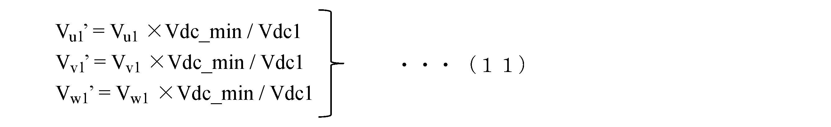
これにより、本実施形態による回転機制御装置1は、系統間でdq軸上における電圧指令が一致するように調整することができる。
これにより、本実施形態による回転機制御装置1は、系統間で、静止座標軸上における電圧指令ベクトルの大きさが一致するように調整することができる。
次に、図面を参照して、第2の実施形態による回転機制御装置1aについて、説明する。
図10は、第2の実施形態による回転機制御装置1aの一例を示すブロック図である。
なお、図10において、図1に示す第1の実施形態と同一の構成には、同一の符号を付与してその説明を省略する。
図11は、本実施形態による回転機制御装置1aの2系統の制御部7aの一例を示すブロック図である。

このように、第1系統の電圧偏差ΔVaは、第1系統の電流Idc1と、第2系統の電流Idc2とのうちの他系統の電流Idc2から自系統の電流Idc1を減算した値に、自系統の直流部電流(電流Idc1)が流れる配線の抵抗を示す配線抵抗Rp(=Rp1)を乗算した値である。


このように、第2系統の電圧偏差ΔVbは、第2系統の電流Idc2と、第1系統の電流Idc1とのうちの他系統の電流Idc1から自系統の電流Idc2を減算した値に、自系統の直流部電流(電流Idc2)が流れる配線の抵抗を示す配線抵抗Rp(=Rp2)を乗算した値である。

本実施形態では、第1の実施形態に比べてインバータ5の配線抵抗(Rp1、Rp2)が存在することにより、直流電圧に電圧降下が生じる。なお、ここでは、Rp1=Rp2=Rpとする。
本実施形態において、回転機制御装置1aは、インバータ5-1とインバータ5-2とが回転機10に供給する電力が一致するように制御するため、下記の式(20)が成り立つ。

例えば、第1系統の検出電圧Vdc1sが、第2系統の検出電圧Vdc2sより大きい場合(Vdc1s>Vdc2s)、上述した式(13)によって、第1系統の電流Idc1は、第2系統の電流Idc2より小さくなる(Idc1<Idc2)。ここで、第2系統においては、上述した式(21)に示される入力電圧Vdc2_realが、インバータ5-2に出力される。


これにより、本実施形態による回転機制御装置1aは、他系統の直流部電流を算出するため、他系統の直流部電流を検出するひつようがない。そのため、本実施形態による回転機制御装置1aは、例えば、センサーなどの検出部の数を低減し、構成を簡略化することができ、低コスト化を実現することができる。
これにより、本実施形態による回転機制御装置1aは、簡易な手法により、容易に他系統の直流部電流を算出することができる。
これにより、本実施形態による回転機制御装置1aは、簡易な手法により、容易に自系統の直流部電流を算出することができる。
次に、図面を参照して、第3の実施形態による回転機制御装置1bについて、説明する。
本実施形態では、3相の各相の自系統電圧を自系統の零相電圧に基づいて補正する変形例について説明する。
図12に示すように、制御信号生成器78a-1は、デューティ演算部781a-1と、キャリア比較部782-1とを備える。なお、図12において、上述した図5と同一の構成には、同一の符号を付与して、その説明を省略する。
制御信号生成器78a-1は、第1直流電圧Vdc1sと、3相軸上の電圧指令値である電圧Vu1、電圧Vv1、及び電圧Vw1とに基づいて、インバータ5-1の制御信号GS11~制御信号GS16を出力する。

零相電圧演算部80-1は、自系統電圧指令(電圧Vu1、電圧Vv1、及び電圧Vw1)の最小のもの(最小電圧Vmin)が、自系統の直流電圧Vdc1sに基づく所定の下限値(例えば、0V)に一致するように、最小電圧Vminに、自系統の直流電圧Vdc1sの2分の1の値(Vdc1s/2)を加算して自系統の零相電圧V0aを算出する。
減算器88-1は、電圧指令値である電圧Vv1に対して、零相電圧V0aを減算した値を、乗算器83-1に出力する。
減算器89-1は、電圧指令値である電圧Vw1に対して、零相電圧V0aを減算した値を、乗算器85-1に出力する。
デューティ演算部781a-1は、下記の式(29)を用いて、第1デューティ(du1、dv1、dw1)を算出する。
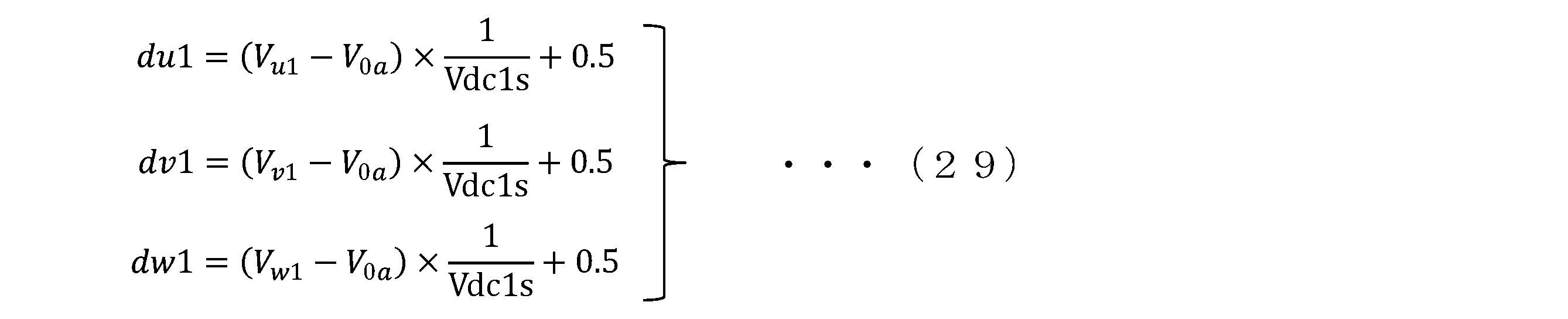
図13は、本実施形態における第2系統の制御信号生成器78a-1の一例を示すブロック図である。
図13に示すように、制御信号生成器78a-2は、デューティ演算部781a-2と、キャリア比較部782-2とを備える。
制御信号生成器78a-2は、第2直流電圧Vdc2sと、3相軸上の電圧指令値である電圧Vu2、電圧Vv2、及び電圧Vw2とに基づいて、インバータ5-2の制御信号GS21~制御信号GS26を出力する。

零相電圧演算部80-2は、自系統電圧指令(電圧Vu2、電圧Vv2、及び電圧Vw2)の最小のもの(最小電圧Vmin)が、自系統の直流電圧Vdc2sに基づく所定の下限値(例えば、0V)に一致するように、最小電圧Vminに、自系統の直流電圧Vdc2sの2分の1の値(Vdc2s/2)を加算して自系統の零相電圧V0bを算出する。
減算器88-2は、電圧指令値である電圧Vv2に対して、零相電圧V0bを減算した値を、乗算器83-2に出力する。
減算器89-2は、電圧指令値である電圧Vw2に対して、零相電圧V0bを減算した値を、乗算器85-2に出力する。

本実施形態による回転機制御装置1bでは、デューティ演算部781a-1及びデューティ演算部781a-2が、自系統の検出電圧(Vdc1s、Vdc2s)を用いて、式(28)及び式(30)により、零相電圧(V0a、V0b)を算出し、零相電圧を、電圧指令値から減算することで、電圧飽和しない範囲でデューティの値を下側にシフトさせる。なお、ここでの説明において、第1系統の制御部7b-1と、第2系統の制御部7b-2とは、同一の構成であるため、各系統を示す符号の「-1」、及び「-2」と、添え字の「1」及び「2」と、零相電圧における[a]及び「b」とを省略して説明する。


図14において、グラフは、横軸が、電圧位相を示す、縦軸が、デューティを示している。また、波形W21、波形W22、波形W23は、それぞれ、U相のデューティの波形、V相のデューティの波形、及びW相のデューティの波形を示している。また、期間TR1は、常時3相がスイッチングされる期間を示している。

図15において、グラフは、横軸が、電圧位相を示す、縦軸が、デューティを示している。また、波形W24、波形W25、波形W26は、それぞれ、U相のデューティの波形、V相のデューティの波形、及びW相のデューティの波形を示している。また、期間TR2は、常時2相がスイッチングされる期間を示している。
これにより、本実施形態による回転機制御装置1bは、電圧飽和しない範囲でデューティの値を下側に適切にシフトすることができる。
次に、図面を参照して、第4の実施形態による回転機制御装置1cについて、説明する。
本実施形態では、3相の各相の自系統電圧を自系統の零相電圧に基づいて補正する別の変形例について説明する。上述した第3の実施形態では、各相の自系統電圧の最小値から零相電圧を算出したが、本実施形態では、各相の自系統電圧の最大値から零相電圧を算出する。
図16に示すように、制御信号生成器78b-1は、デューティ演算部781b-1と、キャリア比較部782-1とを備える。なお、図16において、上述した図12と同一の構成には、同一の符号を付与して、その説明を省略する。
制御信号生成器78b-1は、第1直流電圧Vdc1sと、3相軸上の電圧指令値である電圧Vu1、電圧Vv1、及び電圧Vw1とに基づいて、インバータ5-1の制御信号GS11~制御信号GS16を出力する。

零相電圧演算部80a-1は、自系統電圧指令(電圧Vu1、電圧Vv1、及び電圧Vw1)の最大のもの(最大電圧Vmax)が、自系統の直流電圧Vdc1sに基づく所定の上限値(例えば、Vdc1s)に一致するように、最大電圧Vmaxから、自系統の直流電圧Vdc1sの2分の1の値(Vdc1s/2)を減算して自系統の零相電圧V0aを算出する。
図17は、本実施形態における第2系統の制御信号生成器78b-1の一例を示すブロック図である。
図17に示すように、制御信号生成器78b-2は、デューティ演算部781b-2と、キャリア比較部782-2とを備える。
制御信号生成器78b-2は、第2直流電圧Vdc2sと、3相軸上の電圧指令値である電圧Vu2、電圧Vv2、及び電圧Vw2とに基づいて、インバータ5-2の制御信号GS21~制御信号GS26を出力する。

零相電圧演算部80a-2は、自系統電圧指令(電圧Vu2、電圧Vv2、及び電圧Vw2)の最大のもの(最大電圧Vmax)が、自系統の直流電圧Vdc2sに基づく所定の下限値(例えば、Vdc2s)に一致するように、最大電圧Vmaxに、自系統の直流電圧Vdc2sの2分の1の値(Vdc2s/2)を加算して自系統の零相電圧V0bを算出する。
本実施形態による回転機制御装置1cでは、デューティ演算部781b-1及びデューティ演算部781b-2が、自系統の検出電圧(Vdc1s、Vdc2s)を用いて、式(38)及び式(39)により、零相電圧(V0a、V0b)を算出し、零相電圧を、電圧指令値から減算することで、電圧飽和しない範囲でデューティの値を上側にシフトさせる。なお、ここでの説明において、第1系統の制御部7c-1と、第2系統の制御部7c-2とは、同一の構成であるため、各系統を示す符号の「-1」、及び「-2」と、添え字の「1」及び「2」と、零相電圧における[a]及び「b」とを省略して説明する。


図18において、グラフは、横軸が、電圧位相を示す、縦軸が、デューティを示している。また、波形W31、波形W32、波形W33は、それぞれ、U相のデューティの波形、V相のデューティの波形、及びW相のデューティの波形を示している。また、期間TR3は、常時3相がスイッチングされる期間を示している。

図19において、グラフは、横軸が、電圧位相を示す、縦軸が、デューティを示している。また、波形W34、波形W35、波形W36は、それぞれ、U相のデューティの波形、V相のデューティの波形、及びW相のデューティの波形を示している。また、期間TR4は、常時2相がスイッチングされる期間を示している。
これにより、本実施形態による回転機制御装置1cは、電圧飽和しない範囲でデューティの値を上側に適切にシフトすることができる。
次に、図面を参照して、第5の実施形態による電動パワーステアリング装置100について説明する。
図20は、第5の実施形態による電動パワーステアリング装置100の一例を示すブロック図である。
車輪104は、例えば、自動車などの車両の操舵対象の車輪である。
例えば、上記の各実施形態において、制御目標値(指令値)として回転機10に通電する電流の指令値を用いる例を説明したが、これに限定されるものではない。例えば、回転機10をV/F制御する場合には、制御目標値は、回転機10の速度指令値であり、回転機10の回転位置を制御する場合に、制御目標値は回転機10の位置指令値となる。
また、「コンピュータシステム」は、インターネットやWAN、LAN、専用回線等の通信回線を含むネットワークを介して接続された複数のコンピュータ装置を含んでもよい。また、「コンピュータ読み取り可能な記録媒体」とは、フレキシブルディスク、光磁気ディスク、ROM、CD-ROM等の可搬媒体、コンピュータシステムに内蔵されるハードディスク等の記憶装置のことをいう。このように、プログラムを記憶した記録媒体は、CD-ROM等の非一過性の記録媒体であってもよい。
Claims (12)
- 第1系統の直流電源が出力した第1直流電圧に基づいて、回転機が有する前記第1系統の3相巻線に交流電圧を印加する第1インバータと、
第2系統の直流電源が出力した第2直流電圧に基づいて、前記回転機が有する前記第2系統の3相巻線に交流電圧を印加する第2インバータと、
前記回転機の指令値と、前記第1直流電圧及び第2直流電圧とに基づいて、前記第1インバータへの指令値を生成する第1制御部と、
前記回転機の指令値と、前記第1直流電圧及び第2直流電圧とに基づいて、前記第2インバータへの指令値を生成する第2制御部と
を備え、
前記第1制御部及び前記第2制御部のそれぞれは、
自系統の直流電圧が、他系統の直流電圧より高い場合に、前記他系統の直流電圧によって、自系統の3相巻線に印加する電圧に関する自系統電圧指令を制限するとともに、前記自系統電圧指令を前記自系統の直流電圧によって規格化した値を自系統のインバータへの指令値として生成する
回転機制御装置。 - 前記第1制御部及び前記第2制御部のそれぞれは、
前記自系統の直流電圧に基づいて、自系統の零相電圧を算出し、各相の前記自系統電圧指令を前記自系統の零相電圧に基づいて補正する
請求項1に記載の回転機制御装置。 - 前記第1制御部及び前記第2制御部のそれぞれは、
前記自系統電圧指令の最小のものが、前記自系統の直流電圧に基づく所定の下限値に一致するように、前記自系統の零相電圧を算出する
請求項2に記載の回転機制御装置。 - 前記第1制御部及び前記第2制御部のそれぞれは、
前記自系統電圧指令の最大のものが、前記自系統の直流電圧に基づく所定の上限値に一致するように、前記自系統の零相電圧を算出する
請求項2に記載の回転機制御装置。 - 前記第1制御部及び前記第2制御部のそれぞれは、
前記自系統の直流電圧が前記他系統の直流電圧より高い場合に、前記第1インバータに流れ込む直流部の電流である第1系統の直流部電流と、前記第2インバータに流れ込む直流部の電流である第2系統の直流部電流とのうちの前記他系統の直流部電流から前記自系統の直流部電流を減算した値に、前記自系統の直流部電流が流れる配線の抵抗を示す配線抵抗を乗算した値である電圧偏差に基づいて、前記自系統電圧指令を制限する
請求項1から請求項4のいずれか一項に記載の回転機制御装置。 - 前記第1制御部及び前記第2制御部のそれぞれは、
前記他系統の直流電圧に基づいて、前記他系統の直流部電流を算出する
請求項5に記載の回転機制御装置。 - 前記第1制御部及び前記第2制御部のそれぞれは、
前記自系統の直流電圧と、前記他系統の直流電圧と、前記自系統の直流電流とに基づいて、前記他系統の前記直流部電流を算出する
請求項5又は請求項6に記載の回転機制御装置。 - 各系統の3相巻線に流れる電流を検出する電流検出部を備え、
前記第1制御部及び前記第2制御部のそれぞれは、
前記電流検出部が検出した自系統の3相巻線に流れる電流に基づいて、前記自系統の直流電流を算出する
請求項5から請求項7のいずれか一項に記載の回転機制御装置。 - 前記第1制御部は、第1のCPU(Central Processing Unit)を備え、
前記第2制御部は、第2のCPUを備え、
前記第1のCPUは、前記第1直流電圧を前記第2のCPUに送信し、
前記第2のCPUは、前記第2直流電圧を前記第1のCPUに送信する
請求項1から請求項8のいずれか一項に記載の回転機制御装置。 - 前記第1制御部及び前記第2制御部のそれぞれは、
前記自系統の直流電圧が前記他系統の直流電圧より高い場合に、前記自系統電圧指令のうち、dq軸上における電圧指令を前記他系統の直流電圧によって制限する
請求項1から請求項9のいずれか一項に記載の回転機制御装置。 - 前記第1制御部及び前記第2制御部のそれぞれは、
前記自系統の直流電圧が前記他系統の直流電圧より高い場合に、前記自系統電圧指令のうち、静止座標軸上における電圧指令ベクトルの大きさを、前記他系統の直流電圧によって出力可能な値に制限する
請求項1から請求項9のいずれか一項に記載の回転機制御装置。 - 請求項1から請求項11のいずれか一項に記載の回転機制御装置と、
ステアリングの操舵をアシストする前記回転機と、
前記ステアリングの操舵トルクを検出するトルクセンサと
を備え、
前記回転機制御装置は、前記トルクセンサが検出した前記操舵トルクに応じた前記ステアリングのアシスト指令を、前記回転機の指令値として、前記回転機を制御する
電動パワーステアリング装置。
Priority Applications (5)
| Application Number | Priority Date | Filing Date | Title |
|---|---|---|---|
| CN202180092323.6A CN117044100A (zh) | 2021-04-16 | 2021-04-16 | 旋转电机控制装置以及电动助力转向装置 |
| PCT/JP2021/015673 WO2022219794A1 (ja) | 2021-04-16 | 2021-04-16 | 回転機制御装置、及び電動パワーステアリング装置 |
| EP21936989.9A EP4325716B1 (en) | 2021-04-16 | 2021-04-16 | Rotating machine control device and electric power steering device |
| US18/269,682 US12304577B2 (en) | 2021-04-16 | 2021-04-16 | Rotating machine control device and electric power steering device |
| JP2023514289A JP7412637B2 (ja) | 2021-04-16 | 2021-04-16 | 回転機制御装置、及び電動パワーステアリング装置 |
Applications Claiming Priority (1)
| Application Number | Priority Date | Filing Date | Title |
|---|---|---|---|
| PCT/JP2021/015673 WO2022219794A1 (ja) | 2021-04-16 | 2021-04-16 | 回転機制御装置、及び電動パワーステアリング装置 |
Publications (1)
| Publication Number | Publication Date |
|---|---|
| WO2022219794A1 true WO2022219794A1 (ja) | 2022-10-20 |
Family
ID=83640266
Family Applications (1)
| Application Number | Title | Priority Date | Filing Date |
|---|---|---|---|
| PCT/JP2021/015673 Ceased WO2022219794A1 (ja) | 2021-04-16 | 2021-04-16 | 回転機制御装置、及び電動パワーステアリング装置 |
Country Status (5)
| Country | Link |
|---|---|
| US (1) | US12304577B2 (ja) |
| EP (1) | EP4325716B1 (ja) |
| JP (1) | JP7412637B2 (ja) |
| CN (1) | CN117044100A (ja) |
| WO (1) | WO2022219794A1 (ja) |
Cited By (1)
| Publication number | Priority date | Publication date | Assignee | Title |
|---|---|---|---|---|
| WO2025134669A1 (ja) * | 2023-12-20 | 2025-06-26 | 株式会社デンソー | 回転電機の制御装置、回転電機の制御方法及び回転電機の制御プログラム |
Families Citing this family (2)
| Publication number | Priority date | Publication date | Assignee | Title |
|---|---|---|---|---|
| US12565259B2 (en) * | 2021-04-16 | 2026-03-03 | Mitsubishi Electric Corporation | Rotary machine control device and electric power steering device |
| CN119348703A (zh) * | 2024-12-30 | 2025-01-24 | 上海同驭汽车科技有限公司 | 一种电子助力转向系统 |
Citations (4)
| Publication number | Priority date | Publication date | Assignee | Title |
|---|---|---|---|---|
| JP2011195089A (ja) | 2010-03-23 | 2011-10-06 | Jtekt Corp | 電動パワーステアリング装置 |
| WO2018088465A1 (ja) | 2016-11-11 | 2018-05-17 | 株式会社デンソー | 回転電機制御装置、および、これを用いた電動パワーステアリング装置 |
| JP2018130007A (ja) * | 2016-11-11 | 2018-08-16 | 株式会社デンソー | 回転電機制御装置、および、これを用いた電動パワーステアリング装置 |
| WO2021059436A1 (ja) * | 2019-09-26 | 2021-04-01 | 三菱電機株式会社 | 交流回転機装置 |
Family Cites Families (7)
| Publication number | Priority date | Publication date | Assignee | Title |
|---|---|---|---|---|
| WO2018088463A1 (ja) * | 2016-11-11 | 2018-05-17 | 株式会社デンソー | 回転電機制御装置、および、これを用いた電動パワーステアリング装置 |
| JP6852522B2 (ja) * | 2017-04-03 | 2021-03-31 | 株式会社デンソー | 多相回転機の制御装置 |
| US20200251966A1 (en) * | 2017-10-06 | 2020-08-06 | Nidec Corporation | Motor module, and electric power steering device |
| JP6999480B2 (ja) * | 2018-04-12 | 2022-01-18 | 日立Astemo株式会社 | 電子制御装置及びその診断方法 |
| JP7003863B2 (ja) | 2018-07-20 | 2022-02-04 | トヨタ自動車株式会社 | 車両の制御装置、制御方法および制御プログラム |
| JP7238525B2 (ja) * | 2019-03-25 | 2023-03-14 | 株式会社デンソー | モータ制御装置 |
| JP7230886B2 (ja) * | 2020-06-17 | 2023-03-01 | 株式会社デンソー | モータ制御装置、及び操舵システム |
-
2021
- 2021-04-16 WO PCT/JP2021/015673 patent/WO2022219794A1/ja not_active Ceased
- 2021-04-16 US US18/269,682 patent/US12304577B2/en active Active
- 2021-04-16 EP EP21936989.9A patent/EP4325716B1/en active Active
- 2021-04-16 CN CN202180092323.6A patent/CN117044100A/zh active Pending
- 2021-04-16 JP JP2023514289A patent/JP7412637B2/ja active Active
Patent Citations (4)
| Publication number | Priority date | Publication date | Assignee | Title |
|---|---|---|---|---|
| JP2011195089A (ja) | 2010-03-23 | 2011-10-06 | Jtekt Corp | 電動パワーステアリング装置 |
| WO2018088465A1 (ja) | 2016-11-11 | 2018-05-17 | 株式会社デンソー | 回転電機制御装置、および、これを用いた電動パワーステアリング装置 |
| JP2018130007A (ja) * | 2016-11-11 | 2018-08-16 | 株式会社デンソー | 回転電機制御装置、および、これを用いた電動パワーステアリング装置 |
| WO2021059436A1 (ja) * | 2019-09-26 | 2021-04-01 | 三菱電機株式会社 | 交流回転機装置 |
Non-Patent Citations (1)
| Title |
|---|
| See also references of EP4325716A4 |
Cited By (1)
| Publication number | Priority date | Publication date | Assignee | Title |
|---|---|---|---|---|
| WO2025134669A1 (ja) * | 2023-12-20 | 2025-06-26 | 株式会社デンソー | 回転電機の制御装置、回転電機の制御方法及び回転電機の制御プログラム |
Also Published As
| Publication number | Publication date |
|---|---|
| US20240067258A1 (en) | 2024-02-29 |
| US12304577B2 (en) | 2025-05-20 |
| EP4325716A1 (en) | 2024-02-21 |
| JPWO2022219794A1 (ja) | 2022-10-20 |
| EP4325716A4 (en) | 2024-06-05 |
| JP7412637B2 (ja) | 2024-01-12 |
| CN117044100A (zh) | 2023-11-10 |
| EP4325716B1 (en) | 2025-10-08 |
Similar Documents
| Publication | Publication Date | Title |
|---|---|---|
| US11063544B2 (en) | Inverter device and electric power steering apparatus | |
| US10008970B2 (en) | Control apparatus for AC motor | |
| JP4082444B1 (ja) | 永久磁石同期電動機のベクトル制御装置 | |
| JP7412637B2 (ja) | 回転機制御装置、及び電動パワーステアリング装置 | |
| JP5824918B2 (ja) | インバータ制御装置及びインバータ制御方法 | |
| JP5772843B2 (ja) | 交流電動機の制御装置 | |
| CN109952701B (zh) | 电动机控制装置及具备该电动机控制装置的电动助力转向控制装置 | |
| JP6266161B2 (ja) | 交流回転機の制御装置および電動パワーステアリングの制御装置 | |
| JP7385538B2 (ja) | 電力変換装置、温度推定方法及びプログラム | |
| JP6173520B1 (ja) | 回転電機の制御装置 | |
| JP2019013135A (ja) | 電動パワーステアリング装置 | |
| JP2004289926A (ja) | モーター制御装置 | |
| EP4325714B1 (en) | Rotary machine control device and electric power steering device | |
| JP7529463B2 (ja) | 電力変換装置、電力変換方法及びプログラム | |
| WO2024095475A1 (ja) | モータ制御方法及びモータ制御装置 | |
| JP2022183661A (ja) | 制御装置及び制御方法 | |
| JP7767969B2 (ja) | 巻線界磁型回転電機の制御方法、及び、巻線界磁型回転電機の制御装置 | |
| JP7209656B2 (ja) | モータ制御装置 | |
| JP7676818B2 (ja) | 電力変換装置および電力変換装置の制御方法 | |
| EP4686078A1 (en) | Motor control device | |
| JP4572582B2 (ja) | 誘導電動機の制御装置 | |
| JP2017229127A (ja) | モータの制御装置、及び、制御方法 | |
| WO2024241587A1 (ja) | 制御装置 | |
| JP2024112668A (ja) | オープン巻線型モータの制御方法、及び、オープン巻線型モータの制御装置 | |
| WO2023073823A1 (ja) | 回転機の制御装置及び電動パワーステアリング装置 |
Legal Events
| Date | Code | Title | Description |
|---|---|---|---|
| 121 | Ep: the epo has been informed by wipo that ep was designated in this application |
Ref document number: 21936989 Country of ref document: EP Kind code of ref document: A1 |
|
| ENP | Entry into the national phase |
Ref document number: 2023514289 Country of ref document: JP Kind code of ref document: A |
|
| WWE | Wipo information: entry into national phase |
Ref document number: 18269682 Country of ref document: US |
|
| WWE | Wipo information: entry into national phase |
Ref document number: 202180092323.6 Country of ref document: CN |
|
| WWE | Wipo information: entry into national phase |
Ref document number: 2021936989 Country of ref document: EP |
|
| NENP | Non-entry into the national phase |
Ref country code: DE |
|
| ENP | Entry into the national phase |
Ref document number: 2021936989 Country of ref document: EP Effective date: 20231116 |
|
| WWG | Wipo information: grant in national office |
Ref document number: 18269682 Country of ref document: US |
|
| WWG | Wipo information: grant in national office |
Ref document number: 2021936989 Country of ref document: EP |