WO2022219911A1 - 対象物の距離および/または速度を計測する装置および方法 - Google Patents
対象物の距離および/または速度を計測する装置および方法 Download PDFInfo
- Publication number
- WO2022219911A1 WO2022219911A1 PCT/JP2022/005825 JP2022005825W WO2022219911A1 WO 2022219911 A1 WO2022219911 A1 WO 2022219911A1 JP 2022005825 W JP2022005825 W JP 2022005825W WO 2022219911 A1 WO2022219911 A1 WO 2022219911A1
- Authority
- WO
- WIPO (PCT)
- Prior art keywords
- light
- detection signal
- interference
- optical system
- calibration
- Prior art date
- Legal status (The legal status is an assumption and is not a legal conclusion. Google has not performed a legal analysis and makes no representation as to the accuracy of the status listed.)
- Ceased
Links
Images









Classifications
-
- G—PHYSICS
- G01—MEASURING; TESTING
- G01S—RADIO DIRECTION-FINDING; RADIO NAVIGATION; DETERMINING DISTANCE OR VELOCITY BY USE OF RADIO WAVES; LOCATING OR PRESENCE-DETECTING BY USE OF THE REFLECTION OR RERADIATION OF RADIO WAVES; ANALOGOUS ARRANGEMENTS USING OTHER WAVES
- G01S7/00—Details of systems according to groups G01S13/00, G01S15/00, G01S17/00
- G01S7/48—Details of systems according to groups G01S13/00, G01S15/00, G01S17/00 of systems according to group G01S17/00
- G01S7/491—Details of non-pulse systems
- G01S7/4912—Receivers
- G01S7/4917—Receivers superposing optical signals in a photodetector, e.g. optical heterodyne detection
-
- G—PHYSICS
- G01—MEASURING; TESTING
- G01S—RADIO DIRECTION-FINDING; RADIO NAVIGATION; DETERMINING DISTANCE OR VELOCITY BY USE OF RADIO WAVES; LOCATING OR PRESENCE-DETECTING BY USE OF THE REFLECTION OR RERADIATION OF RADIO WAVES; ANALOGOUS ARRANGEMENTS USING OTHER WAVES
- G01S17/00—Systems using the reflection or reradiation of electromagnetic waves other than radio waves, e.g. lidar systems
- G01S17/02—Systems using the reflection of electromagnetic waves other than radio waves
- G01S17/06—Systems determining position data of a target
- G01S17/08—Systems determining position data of a target for measuring distance only
- G01S17/32—Systems determining position data of a target for measuring distance only using transmission of continuous waves, whether amplitude-, frequency-, or phase-modulated, or unmodulated
- G01S17/34—Systems determining position data of a target for measuring distance only using transmission of continuous waves, whether amplitude-, frequency-, or phase-modulated, or unmodulated using transmission of continuous, frequency-modulated waves while heterodyning the received signal, or a signal derived therefrom, with a locally-generated signal related to the contemporaneously transmitted signal
-
- G—PHYSICS
- G01—MEASURING; TESTING
- G01S—RADIO DIRECTION-FINDING; RADIO NAVIGATION; DETERMINING DISTANCE OR VELOCITY BY USE OF RADIO WAVES; LOCATING OR PRESENCE-DETECTING BY USE OF THE REFLECTION OR RERADIATION OF RADIO WAVES; ANALOGOUS ARRANGEMENTS USING OTHER WAVES
- G01S17/00—Systems using the reflection or reradiation of electromagnetic waves other than radio waves, e.g. lidar systems
- G01S17/02—Systems using the reflection of electromagnetic waves other than radio waves
- G01S17/50—Systems of measurement based on relative movement of target
- G01S17/58—Velocity or trajectory determination systems; Sense-of-movement determination systems
-
- G—PHYSICS
- G01—MEASURING; TESTING
- G01S—RADIO DIRECTION-FINDING; RADIO NAVIGATION; DETERMINING DISTANCE OR VELOCITY BY USE OF RADIO WAVES; LOCATING OR PRESENCE-DETECTING BY USE OF THE REFLECTION OR RERADIATION OF RADIO WAVES; ANALOGOUS ARRANGEMENTS USING OTHER WAVES
- G01S7/00—Details of systems according to groups G01S13/00, G01S15/00, G01S17/00
- G01S7/48—Details of systems according to groups G01S13/00, G01S15/00, G01S17/00 of systems according to group G01S17/00
- G01S7/491—Details of non-pulse systems
- G01S7/4911—Transmitters
-
- G—PHYSICS
- G01—MEASURING; TESTING
- G01S—RADIO DIRECTION-FINDING; RADIO NAVIGATION; DETERMINING DISTANCE OR VELOCITY BY USE OF RADIO WAVES; LOCATING OR PRESENCE-DETECTING BY USE OF THE REFLECTION OR RERADIATION OF RADIO WAVES; ANALOGOUS ARRANGEMENTS USING OTHER WAVES
- G01S7/00—Details of systems according to groups G01S13/00, G01S15/00, G01S17/00
- G01S7/48—Details of systems according to groups G01S13/00, G01S15/00, G01S17/00 of systems according to group G01S17/00
- G01S7/497—Means for monitoring or calibrating
-
- G—PHYSICS
- G01—MEASURING; TESTING
- G01C—MEASURING DISTANCES, LEVELS OR BEARINGS; SURVEYING; NAVIGATION; GYROSCOPIC INSTRUMENTS; PHOTOGRAMMETRY OR VIDEOGRAMMETRY
- G01C3/00—Measuring distances in line of sight; Optical rangefinders
-
- G—PHYSICS
- G01—MEASURING; TESTING
- G01C—MEASURING DISTANCES, LEVELS OR BEARINGS; SURVEYING; NAVIGATION; GYROSCOPIC INSTRUMENTS; PHOTOGRAMMETRY OR VIDEOGRAMMETRY
- G01C3/00—Measuring distances in line of sight; Optical rangefinders
- G01C3/02—Details
- G01C3/06—Use of electric means to obtain final indication
-
- G—PHYSICS
- G01—MEASURING; TESTING
- G01S—RADIO DIRECTION-FINDING; RADIO NAVIGATION; DETERMINING DISTANCE OR VELOCITY BY USE OF RADIO WAVES; LOCATING OR PRESENCE-DETECTING BY USE OF THE REFLECTION OR RERADIATION OF RADIO WAVES; ANALOGOUS ARRANGEMENTS USING OTHER WAVES
- G01S17/00—Systems using the reflection or reradiation of electromagnetic waves other than radio waves, e.g. lidar systems
- G01S17/88—Lidar systems specially adapted for specific applications
- G01S17/93—Lidar systems specially adapted for specific applications for anti-collision purposes
- G01S17/931—Lidar systems specially adapted for specific applications for anti-collision purposes of land vehicles
Definitions
- the present disclosure relates to an apparatus and method for measuring distance and/or velocity of an object.
- a rangefinder based on the FMCW (Frequency Modulated Continuous Wave) method sends out frequency-modulated electromagnetic waves and measures the distance based on the difference in frequency between the transmitted wave and the reflected wave.
- the FMCW rangefinder is called an FMCW radar.
- FMCW radar uses, for example, a voltage controlled oscillator (VCO) as a radio wave oscillation source.
- VCO voltage controlled oscillator
- the FMCW rangefinder is called an FMCW lidar (LiDAR).
- the FMCW lidar uses, for example, a laser light source as a light source.
- An FMCW lidar emits light whose frequency is periodically modulated from a light source toward an object, and the reflected light from the object interferes with the reference light from the light source to obtain interference light.
- the interfering light is detected by a photodetector and converted into an electrical signal.
- This electrical signal contains a signal component with a frequency corresponding to the difference between the frequency of the reflected light and the frequency of the reference light.
- This signal component is called the "beat signal”.
- the frequency of the beat signal is called the "beat frequency”.
- the distance to the object can be calculated based on the beat frequency.
- the velocity of the object can also be calculated using the Doppler shift of the reflected light from the moving object. For example, the velocity of the object can be calculated based on the frequency difference of the beat signal in the up-chirp period during which the frequency of the light emitted from the light source increases and the down-chirp period during which the frequency decreases.
- the FMCW lidar detects the frequency of the electrical signal output from the photodetector, so the distance measurement result is less susceptible to disturbance light.
- the range finding accuracy of FMCW lidar depends on how linearly the frequency of the light can be modulated with respect to time.
- Patent Literature 1 describes that even if the voltage controlled oscillator of the FMCW radar sweeps the voltage linearly with respect to time, the frequency changes nonlinearly, resulting in deterioration of the ranging performance. .
- Patent Document 1 discloses a method of dynamically changing the sampling timing of the interference signal based on the sweep signal obtained from the artificial target. It is described that this can compensate for the nonlinearity of the frequency sweep.
- Patent Document 2 discloses an FMCW radar device that corrects the frequency of an interference signal using correction data corresponding to multiple distances and multiple ambient temperatures. It is described that this improves the detection accuracy.
- Patent Document 3 discloses an example of an FMCW lidar device that continuously measures the frequency of beat signals and calculates the distance to an object based on the average value of the measured frequencies. It is described that this eliminates the effects of laser nonlinear chirp and enables accurate distance measurement.
- Patent Document 4 discloses an ophthalmic device used to identify the position of a measurement target site inside the human eye.
- This ophthalmologic apparatus includes a measurement optical system, a reference optical system, a calibration optical system, a light receiving element, and an arithmetic device.
- the measurement optical system irradiates the interior of the subject's eye with light from the light source and guides the reflected light.
- the reference optical system guides the light from the light source as reference light.
- Calibration optics guide the light from the light source.
- the light-receiving element emits measurement interference light obtained by synthesizing the reflected light guided by the measurement optical system and the reference light guided by the reference optical system, the calibration light guided by the calibration optical system, and the reference light guided by the reference optical system.
- the interference light for calibration combined with the reference light is received.
- the computing device identifies the position of the measurement target site inside the subject's eye based on the interference light for measurement and the interference light for calibration received by the light receiving element. It is described that with such a configuration, even if the characteristics of the interference light change with the passage of time, the position of the measurement target site inside the subject's eye can be specified accurately.
- the present disclosure provides a measurement device that utilizes FMCW technology, even if the output characteristics of the light source change due to the passage of time, changes in the usage environment, changes in the operating state of the light source, etc.
- a technique capable of suppressing deterioration in measurement accuracy is provided.
- a measuring device includes a light source, a calibration optical system, an interference optical system, a light receiving device, a storage device, and a processing circuit.
- the light source emits frequency-modulated light.
- the calibration optics have at least one reflective surface.
- the interference optical system separates the light emitted from the light source into reference light and output light, and is interference light between the reflected light generated when the output light is reflected by an object and the reference light.
- First interference light and second interference light which is interference light between the reflected light generated by reflecting the output light from the calibration optical system and the reference light, are generated.
- the light receiving device has at least one photodetector and outputs a first detection signal corresponding to the intensity of the first interference light and a second detection signal corresponding to the intensity of the second interference light.
- the storage device stores correction data used for correcting the first detection signal.
- the processing circuit sends to the light source a control signal for sweeping the frequency of the light emitted from the light source, updates the correction data based on the second detection signal, and updates the correction data. and generating and outputting measurement data relating to the distance and/or velocity of the object based on the corrected first detection signal.
- the present disclosure may be realized by a system, apparatus, method, integrated circuit, computer program, or recording medium such as a computer-readable recording disk. It may be realized by any combination of computer program and recording medium.
- the computer-readable recording medium may include a volatile recording medium, or may include a non-volatile recording medium such as a CD-ROM (Compact Disc-Read Only Memory).
- a device may consist of one or more devices. When the device is composed of two or more devices, the two or more devices may be arranged in one device, or may be divided and arranged in two or more separate devices. As used herein and in the claims, a "device" can mean not only one device, but also a system of multiple devices.
- the accuracy of distance and/or velocity measurement decreases. can be suppressed.
- FIG. 1 is a diagram showing data obtained from experiments conducted by the present inventors.
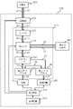
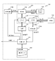
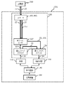
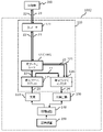
- FIG. 2 is a block diagram showing a schematic configuration of a measuring device according to an exemplary embodiment;
- FIG. 3 is a block diagram showing a configuration example of a light source and an interference optical system.
- FIG. 4 is a diagram showing an example of the control signal output from the processing circuit and the drive current signal output from the drive circuit.
- FIG. 5A is a diagram showing an example of a calibration optical system.
- FIG. 5B is a diagram showing another example of the calibration optical system.
- FIG. 5C is a diagram showing still another example of the calibration optical system.
- FIG. 6 is a block diagram showing a configuration example of a measuring device whose interference optical system is a fiber optical system.
- FIG. 7 is a block diagram showing an example of a measuring device having an optical deflector.
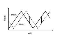
- FIG. 8A is a diagram schematically showing an example of temporal changes in frequencies of reference light and reflected light when the object is stationary.
- FIG. 8B is a diagram schematically showing temporal changes in the frequencies of reference light and reflected light when an object approaches measuring apparatus 100 .
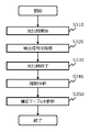
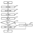
- FIG. 9 is a flowchart showing an example of calibration operation.
- FIG. 10A is a graph showing an example of analysis results of the period of the detection signal.
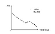
- FIG. 10B is a diagram showing an example of the relationship between control signal voltage and period.
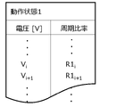
- FIG. 11A shows an example of a correction table associated with the first operating state of the light source.
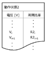
- FIG. 11B shows an example of a correction table associated with the second operating state of the light source.
- FIG. 12 is a diagram showing examples of waveforms of detection signals before and after correction.
- FIG. 13 is a diagram showing an example of a conversion table that defines the relationship between beat signal frequency and distance.
- FIG. 14A is a diagram showing an example of a conversion table that defines the relationship between the frequency of the beat signal and the distance corresponding to the first operating state.
- FIG. 14B is a diagram showing an example of a conversion table that defines the relationship between the frequency of the beat signal and the distance corresponding to the second operating state.
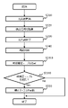
- FIG. 15 is a flow chart showing an example of the distance measurement operation.
- FIG. 16 is a block diagram showing a schematic configuration of a measuring device according to another embodiment.
- FIG. 17 is a block diagram showing a schematic configuration of a measuring device according to still another embodiment.
- FIG. 16 is a block diagram showing a schematic configuration of a measuring device according to another embodiment.
- FIG. 18 is a block diagram showing a schematic configuration of a measuring device according to still another embodiment.
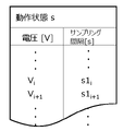
- FIG. 19A is a diagram showing an example of a correction table that defines the relationship between the voltage of the control signal and the sampling interval.
- FIG. 19B is a diagram showing an example of a correction table that defines the relationship between the phase of frequency modulation and the period ratio.
- FIG. 19C is a diagram showing an example of a correction table that defines the relationship between the phase of frequency modulation and the sampling interval.
- FIG. 20 is a block diagram showing a schematic configuration of a measuring device according to another embodiment.
- FIG. 21 is a block diagram showing a schematic configuration of a measuring device according to a first modified example of the embodiment of the present disclosure; FIG.
- FIG. 22 is a block diagram showing a schematic configuration of a measuring device according to a second modified example of the embodiment of the present disclosure
- FIG. 23 is a flow chart showing calibration operation of the measuring device according to the third modification of the embodiment of the present disclosure.
- FIG. 24 is a flow chart showing calibration operation of the measuring device according to the fourth modification of the embodiment of the present disclosure.
- FIG. 1 shows an example of data obtained from experiments conducted by the present inventors.
- a laser beam was emitted from a semiconductor laser light source placed at a stationary point toward a reflecting plate, which is a stationary object.
- control voltage the voltage of the control signal input to the light source
- Vm a predetermined voltage range
- modulation voltage amplitude a predetermined voltage range
- the light source A laser beam whose frequency was periodically modulated was emitted from the laser beam.
- the reflected light from the reflector and the emitted light from the light source were caused to interfere, the interference light was detected by a photodetector, and the acquired signal was recorded.
- Graph (a) in FIG. 1 shows an example of the change over time of the voltage of the control signal input to the light source.
- the control signal is swept linearly with time over the voltage range Vm1 .
- the median value of the voltage range (hereinafter also referred to as "bias voltage") is Vb .
- Graph (b) of FIG. 1 shows an example of the time change of the control voltage when the same laser light source is controlled under the same temperature condition with different control signals.
- the bias voltage is Vb as in example (a), but the modulation voltage amplitude is Vm2 .
- V m2 is 1.5 times V m1 .
- Graphs (c) and (d) in FIG. 1 show the reflected light generated when the laser light is emitted from the light source toward a stationary reflector and the reference light that travels from the light source to the photodetector via the optical system.
- An example of a waveform of an electrical signal (hereinafter also referred to as a "detection signal") obtained by detecting interference light is shown.
- Graphs (c) and (d) show the waveforms of the detection signal when the modulation voltage amplitudes are Vm1 and Vm2 , respectively.
- the time axes in these graphs are the same as those in graphs (a) and (b).
- Graphs (a) to (d) represent changes in the signal for one cycle of the control voltage.
- the cycle of the control voltage may be referred to as "modulation cycle”.
- Graphs (e) and (f) in FIG. 1 show temporal changes in the instantaneous frequency of the beat signal obtained by frequency analysis of the signal waveforms of graphs (c) and (d), respectively.
- the waveforms of graphs (e) and (f) were obtained based on the signal voltage ranging from time t1 to t2 in graphs (c) and (d), respectively .
- Graph (g) in FIG. 1 plots the instantaneous frequencies corresponding to the two modulation voltage amplitudes Vm1 and Vm2 in relation to the voltage of the control signal.
- the stationary object was illuminated with light, so if the frequency of the light was also linearly swept in response to the linear sweep of the control voltage, the frequency of the beat signal would be constant regardless of time.
- the frequency of the beat signal fluctuates over time.
- the nonlinearity of the frequency of the beat signal with respect to time differs between when the modulation voltage amplitude is Vm1 and when it is Vm2 . This indicates that the nonlinearity of the frequency change of light with respect to time differs depending on the magnitude of the modulation voltage amplitude.
- the nonlinearity of the fluctuation of the frequency of the beat signal is It is different between the case and the case of V m2 .
- the frequency of the beat signal tends to increase relatively with increasing control voltage on the high voltage side
- the modulation current amplitude of Vm2 the frequency is the same.
- a saturation tendency is seen at the control voltage on the high voltage side.
- a similar phenomenon may also occur when the characteristics of the light source change due to various factors such as changes in usage environment such as temperature or humidity, passage of time, or vibration. Even if the characteristics of the light source change, it is required to suppress deterioration in measurement accuracy.
- a measuring device includes a light source, a calibration optical system, an interference optical system, a light receiving device, a storage device, and a processing circuit.
- the light source emits frequency-modulated light.
- the calibration optics have at least one reflective surface.
- the interference optical system separates the light emitted from the light source into reference light and output light, and is interference light between the reflected light generated when the output light is reflected by an object and the reference light.
- First interference light and second interference light which is interference light between the reflected light generated by reflecting the output light from the calibration optical system and the reference light, are generated.
- the light receiving device has at least one photodetector and outputs a first detection signal corresponding to the intensity of the first interference light and a second detection signal corresponding to the intensity of the second interference light.
- the storage device stores correction data used for correcting the first detection signal.
- the processing circuit sends to the light source a control signal for sweeping the frequency of the light emitted from the light source, updates the correction data based on the second detection signal, and updates the correction data. and generating and outputting measurement data relating to the distance and/or velocity of the object based on the corrected first detection signal.
- the processing circuit updates the correction data based on the measurement result of the second interference light using the calibration optical system, and generates the first detection signal based on the updated correction data. can be corrected appropriately.
- distance and/or velocity can be measured with high accuracy even if the output characteristics of the light source change due to, for example, deterioration over time, changes in usage environment, or changes in operating conditions of the light source.
- the correction data can be created, for example, by calibration performed before shipment by the manufacturer of the measuring device, and recorded in the storage device.
- the operation of updating the correction data is performed by the user of the measuring device. The user can cause the measuring device to perform an operation for updating the correction data at any timing before or during the measurement.
- the updating of the correction data may be an operation of correcting and overwriting the existing correction data, an operation of rewriting the existing correction data to new correction data, or an operation of rewriting the existing correction data. It may be an operation of recording new correction data while leaving the correction data. If there is no existing correction data in the storage device, the correction data may be updated by creating new correction data.
- the operation of creating new correction data may be performed at the time of calibration performed by the manufacturer of the measuring device before shipment. In the present disclosure, for the sake of convenience, such an operation of newly creating correction data is also referred to as "updating" correction data.
- the interference optical system may include an optical switch that switches between a first state in which the output light is emitted to the object and a second state in which the output light is emitted to the calibration optical system.
- the processing circuitry may operate in a measurement mode for measuring the distance and/or speed of the object and a calibration mode for updating the correction data.
- the processing circuit sets the optical switch to the first state, corrects the first detection signal based on the correction data, and corrects the measurement data based on the corrected first detection signal. may be generated.
- the processing circuit may set the optical switch to the second state and update the correction data based on the second detection signal.
- the measuring device may further include a time counter that measures the usage time of the light source.
- the processing circuit may switch between the measurement mode and the calibration mode based on the usage time of the light source. For example, the processing circuitry may switch from the measurement mode to the calibration mode when the usage time of the light source since the correction data was last updated exceeds a certain threshold.
- the processing circuitry may switch from the measurement mode to the calibration mode when the usage time of the light source since the correction data was last updated exceeds a certain threshold.
- the measuring device may further include a temperature sensor that measures the temperature of the light source.
- the processing circuitry may switch between the measurement mode and the calibration mode based on the temperature of the light source. For example, the processing circuitry may switch from a measurement mode to a calibration mode if the measured temperature of the light source is outside a predetermined range.
- the predetermined range can be set to include, for example, the temperature when the correction data was created or last updated.
- the processing circuitry may switch from the measurement mode to the calibration mode when the measured temperature of the light source is below or above a threshold.
- the processing circuit may switch between the measurement mode and the calibration mode in response to an input from a user. For example, the processing circuit may switch from the measurement mode to the calibration mode when the user performs an operation to instruct the start of the calibration mode using an input device built in or connected to the measurement device. This allows the user to update the correction data at any timing.
- the processing circuit may switch to the calibration mode when the operation state of the light source is changed by changing the control signal in the measurement mode.
- the processing circuitry may switch to a calibration mode when changing the amplitude of the control voltage applied to the light source to change the range of measurable distances. This makes it possible to mitigate the effects of non-linear frequency modulation, which occurs differently depending on the operating state of the light source, and enables more precise measurement of distance and/or velocity.
- the storage device may further store a reference distance according to the optical path length of the calibration optical system.
- the processing circuit may update the correction data based on the second detection signal and the reference distance.
- a reference distance can be, for example, the optical distance from the light source to a particular reflective surface of the calibration optics.
- the processing circuit generates, as updated correction data, correction data for correcting the second detection signal so that the distance theoretically derived from the frequency of the second detection signal matches the reference distance, for example. can do.
- a measurable distance range can be set in the measuring device.
- the reference distance may be included in the distance range. For example, if the measurable distance range is from 0m to 100m, the reference distance may be set to a distance within that range, such as 50m. Thus, by using a distance close to the actually measured distance as the reference distance, it is possible to correct the correction data more appropriately.
- the interference optical system may include optical fibers, mirrors, or multipass cells. By using an interference optical system including these optical elements, it becomes easier to secure a relatively long optical path length, and the quality of calibration can be improved.
- the correction data may include correction value information corresponding to each of the plurality of voltage values or the plurality of current values in the control signal.
- the correction value can be, for example, a coefficient for correcting the period of the detection signal.
- the processing circuitry may correct the detected signal by determining the period from the detected signal and multiplying the period by the correction value.
- the correction data may include correction value information corresponding to each of a plurality of phases or a plurality of timings in frequency modulation by the control signal. Based on the correction data including information on such correction values, the processing circuit can appropriately correct the detection signal.
- the correction data may include correction value information for changing sampling timing when the processing circuit samples the detection signal.
- the processing circuit can correct the detection signal by determining the sampling timing of the detection signal according to the correction value.
- the correction data may be data indicating a correction table or a correction function for determining correction values used to correct the detection signal.
- the processing circuitry can appropriately correct the detected signal based on the correction values determined based on the correction table or correction function.
- a method according to another embodiment of the present disclosure is performed by a computer in a system including a measurement device.
- the measuring device comprises a light source emitting light whose frequency is periodically modulated, a calibration optical system having at least one reflecting surface, and separating the light emitted from the light source into reference light and output light.
- a first interference light that is interference light between the output light reflected by the object and the reference light and the output light reflected by the calibration optical system
- An interference optical system that generates a second interference light that is interference light with the reference light, and at least one photodetector, a first detection signal according to the intensity of the first interference light, and the second interference
- a light-receiving device that outputs a second detection signal according to the intensity of light, and a storage device that stores correction data used for correcting the first detection signal.
- the method includes updating the correction data based on the second detection signal, correcting the first detection signal based on the updated correction data, and correcting the first detection. generating and outputting measurement data regarding the distance and/or velocity of the object based on the signal.
- a computer program according to still another embodiment of the present disclosure is executed by a computer in a system including a measuring device.
- the computer program is stored in a computer-readable non-transitory recording medium.
- the measuring device comprises a light source emitting light whose frequency is periodically modulated, a calibration optical system having at least one reflecting surface, and separating the light emitted from the light source into reference light and output light.
- a first interference light that is interference light between the output light reflected by the object and the reference light and the output light reflected by the calibration optical system
- An interference optical system that generates a second interference light that is interference light with the reference light, and at least one photodetector, a first detection signal according to the intensity of the first interference light, and the second interference
- a light-receiving device that outputs a second detection signal according to the intensity of light, and a storage device that stores correction data used for correcting the first detection signal.
- the computer program causes the computer to update the correction data based on the second detection signal, correct the first detection signal based on the updated correction data, and correct the and generating and outputting measurement data relating to the distance and/or speed of the object based on the first detection signal.
- all or part of a circuit, unit, device, member or section, or all or part of a functional block in a block diagram is, for example, a semiconductor device, a semiconductor integrated circuit (IC), or an LSI (large scale integration). ) may be performed by one or more electronic circuits.
- An LSI or IC may be integrated on one chip, or may be configured by combining a plurality of chips.
- functional blocks other than memory elements may be integrated into one chip.
- LSIs or ICs may be called system LSIs, VLSIs (very large scale integration), or ULSIs (ultra large scale integration) depending on the degree of integration.
- a Field Programmable Gate Array (FPGA), which is programmed after the LSI is manufactured, or a reconfigurable logic device that can reconfigure the connection relationships inside the LSI or set up the circuit partitions inside the LSI can also be used for the same purpose.
- FPGA Field Programmable Gate Array
- circuits, units, devices, members or parts can be executed by software processing.
- the software is recorded on one or more non-transitory storage media, such as ROMs, optical discs, hard disk drives, etc., such that when the software is executed by a processor, the functions specified in the software are performed. It is executed by processors and peripherals.
- a system or apparatus may comprise one or more non-transitory storage media on which software is recorded, a processor, and required hardware devices such as interfaces.
- the measuring device of this embodiment is a distance measuring device that measures the distance to an object using FMCW-LiDAR technology.
- the measuring device may measure the velocity of the object in addition to the distance or instead of the distance.
- the measurement device may be mounted on a mobile object, such as an autonomous vehicle, an automated guided vehicle (AGV), an unmanned aerial vehicle (UAV), or a mobile robot.
- a mobile object such as an autonomous vehicle, an automated guided vehicle (AGV), an unmanned aerial vehicle (UAV), or a mobile robot.
- a mobile object such as an autonomous vehicle, an automated guided vehicle (AGV), an unmanned aerial vehicle (UAV), or a mobile robot.
- AGV automated guided vehicle
- UAV unmanned aerial vehicle
- the measuring device is not limited to mobile objects, and can be used by being mounted on any device.
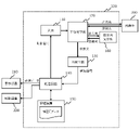
- FIG. 2 is a block diagram showing a schematic configuration of the measuring device 100 according to this embodiment.
- thick arrows represent the flow of light
- thin arrows represent the flow of signals or data.
- object 300 whose distance and/or velocity is to be measured, and a display device 210 and a control device 220 connected to the measurement device 100 .
- Object 300 is any object such as, for example, an obstacle, a person, or a mobile object (eg, an automobile, a two-wheeled vehicle, a mobile robot, or a drone).
- the measuring device 100 shown in FIG. 2 includes a light source 110, an interference optical system 120, a photodetector 130, a processing circuit 140, a storage device 150, and a calibration optical system 180.
- Light source 110 can change the frequency of emitted light in response to a control signal output from processing circuitry 140 .
- the interference optical system 120 separates the light emitted from the light source 110 into reference light and output light, and causes the reflected light generated by the output light to be reflected by the object 300 or the calibration optical system 180 to interfere with the reference light. to generate interference light. Interference light between the reflected light reflected by the object 300 and the reference light is referred to as "first interference light".
- Interference light between the reflected light reflected by the calibration optical system 180 and the reference light is referred to as "second interference light". These interfering lights are incident on photodetector 130 .
- the calibration optical system 180 is used in a calibration operation for updating correction data stored in the storage device 150 .
- Calibration optics 180 includes one or more optical elements having at least one reflective surface. Detailed configurations of the light source 110, the interference optical system 120, and the calibration optical system 180 will be described later.
- the photodetector 130 receives the interference light, generates and outputs an electrical signal corresponding to the intensity of the interference light. This electrical signal is called a "detection signal”.
- a detection signal based on the first interference light is referred to as a "first detection signal”
- a detection signal based on the second interference light is referred to as a "second detection signal”.
- Photodetector 130 includes one or more light receiving elements.
- the light receiving element includes, for example, a photoelectric conversion element such as a photodiode.
- the photodetector 130 may be a sensor with multiple light receiving elements, such as an image sensor. In this embodiment, one photodetector 130 detects both the first interference light and the second interference light.
- a photodetector for detecting the first interference light and a photodetector for detecting the second interference light may be separately provided as in another embodiment described later. In that case, an interference optical system that generates the first interference light and an interference optical system that generates the second interference light can be provided separately.
- a device comprising at least one photodetector is referred to herein as a receiver device. The light receiving device generates and outputs a first detection signal corresponding to the intensity of the first interference light and a second detection signal corresponding to the intensity of the second interference light.
- the processing circuit 140 is an electronic circuit that controls the light source 110 and performs processing based on the detection signal output from the photodetector 130 .
- Processing circuitry 140 may include control circuitry for controlling light source 110 and signal processing circuitry for performing signal processing based on the detection signals.
- the processing circuit 140 may be configured as one circuit, or may be an aggregate of a plurality of separate circuits.
- Processing circuitry 140 sends control signals to light source 110 .
- the control signal causes the light source 110 to periodically change the frequency of the emitted light within a predetermined range. In other words, the control signal is a signal that sweeps the frequency of light emitted from light source 110 .
- the control signal is a signal that inputs a voltage or current that periodically fluctuates with a certain amplitude to the light source 110 .
- the processing circuit 140 in this embodiment operates by switching between a measurement mode for measuring the distance and/or speed of the object 300 and a calibration mode for updating correction data.
- the processing circuit 140 acquires the first detection signal output from the photodetector 130 while the light source 110 is emitting frequency-modulated light, and stores the first detection signal in the storage device 150. Correction is performed based on the stored correction data.
- the correction data may be, for example, data defining a correspondence relationship between the voltage of the control signal and a correction value for correcting the period or frequency of the detection signal. Details of the correction data will be described later.
- Processing circuitry 140 determines the distance to object 300 and/or the velocity of object 300 based on the corrected first detection signal using the correction data.
- Processing circuitry 140 generates and outputs data indicative of the distance and/or velocity. This data is hereinafter referred to as "measurement data".
- the processing circuit 140 obtains the second detection signal output from the photodetector 130 while the light source 110 is emitting frequency-modulated light, The correction data is corrected based on the reference distance set according to the optical path length of the optical system 180 for correction.
- Processing circuitry 140 updates the existing correction data with the corrected correction data. In subsequent measurements, the processing circuit 140 corrects the first detection signal using the updated correction data to generate measurement data.
- the storage device 150 includes arbitrary storage media such as semiconductor memory, magnetic disk, and optical disk.
- the storage device 150 stores correction data used in correction processing executed by the processing circuit 140 and reference distance data corresponding to the optical path length of the calibration optical system 180 .
- Correction data may include, for example, one or more correction tables.
- the correction data may contain multiple correction tables.
- Each of the plurality of correction tables may be associated and recorded with a corresponding one of a plurality of different operating states of light source 110 .
- the operating state of the light source 110 may be, for example, a state characterized by the aforementioned modulation voltage amplitude, bias voltage, or temperature of the light source 110 .
- the correction data is not limited to the correction table, and may be data in any format such as a function.
- Storage device 150 also stores computer programs that are executed by processing circuitry 140 .
- the processing circuit 140 and the storage device 150 may be integrated on one circuit board, or may be provided on separate circuit boards.
- the functionality of processing circuitry 140 may be distributed over multiple circuits. At least part of the functions of the processing circuitry 140 may be implemented by an external computer installed at a location remote from other components. Such an external computer controls the operation of light source 110 and photodetector 130 and/or performs signal processing based on the detection signal output from photodetector 130 via a wired or wireless communication network.
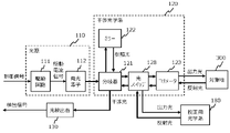
- FIG. 3 is a block diagram showing a configuration example of the light source 110 and the interference optical system 120.
- the light source 110 in this example comprises a driving circuit 111 and a light emitting element 112 .
- the drive circuit 111 receives the control signal output from the processing circuit 140 , generates a drive current signal according to the control signal, and inputs the drive current signal to the light emitting element 112 .
- the light emitting element 112 may be an element that emits highly coherent laser light, such as a semiconductor laser element.
- the light emitting element 112 emits frequency-modulated laser light in response to the drive current signal.
- the frequency of the laser light emitted from the light emitting element 112 is modulated at a constant cycle.
- the frequency modulation period can be, for example, 1 microsecond ( ⁇ s) or more and 10 milliseconds (ms) or less.
- the frequency modulation amplitude can be, for example, greater than or equal to 100 MHz and less than or equal to 1 THz.
- the wavelength of the laser light can be included in the near-infrared wavelength range of 700 nm or more and 2000 nm or less, for example. In sunlight, the amount of near-infrared light is smaller than the amount of visible light. Therefore, by using near-infrared light as the laser light, the influence of sunlight can be reduced.
- the wavelength of the laser light may be included in the visible light wavelength range of 400 nm or more and 700 nm or less or the ultraviolet light wavelength range.
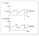
- FIG. 4 is a diagram showing an example of the control signal output from the processing circuit 140 and the drive current signal output from the drive circuit 111.
- FIG. Parts (a) and (b) of FIG. 4 show examples of waveforms of the control signal and the drive current signal, respectively.
- the control signal applies a voltage that fluctuates with a predetermined period and a predetermined amplitude to the driving circuit 111 of the light source 110 .
- the voltage of the control signal may be modulated in a sawtooth waveform.
- the voltage of the control signal is not limited to a sawtooth waveform, and may be modulated in a triangular waveform.
- the frequency of the light emitted from the light emitting element 112 can be swept in a near-linear form by a control signal in which the voltage repeats a linear change such as a sawtooth wave or a triangular wave.
- a control signal in which the voltage repeats a linear change such as a sawtooth wave or a triangular wave.
- frequency sweeps are not perfectly linear.
- the amplitude of the modulation waveform of such a control signal is called modulation voltage amplitude, and the voltage at the center of the modulation range is called bias voltage.
- the control signal applies a voltage that fluctuates around the bias voltage to the driving circuit 111 of the light source 110 .
- the drive circuit 111 converts the control signal into a drive current signal and drives the light emitting element 112 with the drive current signal.
- the drive current signal changes with a waveform corresponding to the control signal.
- the modulation range or amplitude of the drive current signal is called the modulation current amplitude, and the current in the center of the modulation range is called the bias current.
- the driving current signal increases and the frequency of the laser light emitted from the light emitting element 112 increases (that is, the wavelength shortens).
- the drive current signal decreases and the frequency of the laser light emitted from the light emitting element 112 decreases (that is, the wavelength lengthens).
- the interference optical system 120 in the example shown in FIG. 3 includes a splitter 121, a mirror 122, an optical switch 128, and a collimator 123.
- the branching device 121 splits the laser light emitted from the light emitting element 112 of the light source 110 into reference light and output light, and combines the reflected light from the object 300 or the calibration optical system 180 with the reference light to produce interference light.
- to generate Mirror 122 reflects the reference light back to splitter 121 .
- the optical switch 128 switches the output destination of output light between the collimator 123 and the calibration optical system 180 .
- the optical switch 128 can switch between a first state in which the output light is emitted to the object 300 and a second state in which the output light is emitted to the calibration optical system 180 .
- the operation of optical switch 128 is controlled by processing circuitry 140 .
- the processing circuit 140 puts the optical switch 128 in the first state and causes the output light 22 to enter the collimator 123 .
- the processing circuitry 140 places the optical switch 128 in the second state and directs the output light 22 into the calibration optics 180 .
- the collimator 123 includes a collimating lens, and irradiates the object 300 with the output light output from the optical switch 128 with a spread angle close to parallel.
- Calibration optics 180 has at least one reflective surface. The calibration optical system 180 reflects the output light output from the optical switch 128 on the reflecting surface and returns the reflected light to the optical switch 128 .
- FIG. 5A to 5C are diagrams schematically showing examples of the calibration optical system 180.
- FIG. FIG. 5A shows an example of calibration optics 180 including optical fiber 180A. In this example, output light from optical switch 128 is reflected back to optical switch 128 by reflecting surface 181 at the end of optical fiber 180A.
- FIG. 5B shows an example of calibration optics 180 including mirror 180B. In this example, the output light from optical switch 128 is reflected by the reflective surface of mirror 180B and returns to optical switch 128.
- FIG. FIG. 5C shows an example of calibration optics 180 including a multipass cell 180C. In this example, the output light from the optical switch 128 is multiple-reflected by the reflective surfaces of the mirrors included in the multipass cell and returns to the optical switch 128 .
- a measurable distance range (for example, 0 m to 50 m) is set for the measuring device 100 .
- a reference distance determined according to the optical path length is set in the calibration optical system 180 and recorded in the storage device 150 .
- Calibration optical system 180 can be designed such that its reference distance is included in the measurable distance range of measuring apparatus 100 .
- the optical path length from the optical switch 128 to the reflecting surface 181 at the end of the optical fiber 180A can be set as the reference distance.
- the optical path length from optical switch 128 to the reflecting surface of mirror 180B can be set as the reference distance.
- FIG. 5A the optical path length from optical switch 128 to the reflecting surface of mirror 180B can be set as the reference distance.
- the optical path length from optical switch 128 through multipass cell 180C and back to optical switch 128 may be set as the reference distance.
- Calibration optical system 180 can be designed such that these reference distances are within the range of distances that can be measured by measuring apparatus 100 . With such a configuration, the optical path length of light from the optical switch 128 through the calibration optical system 180 and back to the optical switch 128 becomes close to the optical path length assumed at the time of measurement. This makes it possible to reduce the influence of reflection noise at a short distance inside the apparatus, and avoid problems such as the beat frequency being too low to be measured when the distance is too short. As an example, consider a case where the range of distances measurable by the measuring device 100 is from 0 m to 20 m.
- the length of optical fiber 180A in the example of FIG. 5A, the optical path length from optical switch 128 to mirror 180B in the example of FIG. Half of the optical path length to the return can be designed to a value within the range of several tens of centimeters to several tens of meters, for example.
- the optical path length may be increased by bending or winding the optical fiber 180A.
- other mirrors or other optical elements may be combined to increase the optical path length.
- the interference optical system 120 is not limited to the configuration shown in FIG. 3, and may include, for example, a fiber optical system. In that case, a fiber coupler can be used as the splitter 121 .
- the reference light does not necessarily need to be reflected by the mirror 122 , and may be returned to the splitter 121 by routing an optical fiber, for example.
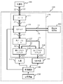
- FIG. 6 is a block diagram showing a configuration example of the measuring device 100 in which the interference optical system 120 includes a fiber optical system.
- interference optical system 120 includes first fiber splitter 125 , second fiber splitter 126 and optical circulator 127 in addition to collimator 123 and optical switch 128 .
- the first fiber splitter 125 splits the laser light 20 emitted from the light source 110 into reference light 21 and output light 22 .
- the first fiber splitter 125 causes the reference light 21 to enter the second fiber splitter 126 and the output light 22 to enter the optical circulator 127 .
- the optical circulator 127 causes the output light 22 to enter the optical switch 128 and causes the reflected light 23 from the optical switch 128 to enter the second fiber splitter 126 .
- the second fiber splitter 126 causes the interference light 24 between the reference light 21 and the reflected light 23 to enter the photodetector 130 .
- the optical switch 128 causes the output light 22 to enter one of the collimator 123 and the calibration optical system 180 according to a command from the processing circuit 140 .
- the collimator 123 shapes the beam shape of the output light 22 and emits the output light 22 toward the object 300 .
- the measuring device 100 may further include an optical deflector that changes the direction of emitted light.
- FIG. 7 is a block diagram showing an example of the measuring device 100 including the optical deflector 170.
- the optical deflector 170 may include, for example, a MEMS (Micromechanical Electrosystem) mirror or a galvanomirror.
- the optical deflector 170 can change the emission direction of the output light 22 by changing the angle of the mirror according to the instruction from the processing circuit 140 . Thereby, beam scanning can be realized.
- the optical deflector 170 is not limited to the above configuration.
- Optical deflector 170 may be, for example, a beam scanning device using an optical phased array and slow light waveguides, as described in WO2019/130720.
- FIG. 8A is a diagram schematically showing an example of temporal changes in the frequencies of the reference light and the reflected light when the object 300 is stationary.
- the frequency changes like a triangular wave will be described.
- the solid line represents the reference light
- the dashed line represents the reflected light.
- the frequency of the reference light shown in FIG. 8A linearly increases during the modulation period and then linearly decreases by the increased amount.
- the frequency of the reflected light is shifted along the time axis by the amount of time it takes for the light to exit the measurement device 100 and be reflected back by the object 300 compared to the frequency of the reference light.
- interference light between the reference light and the reflected light has a frequency corresponding to the difference between the frequency of the reflected light and the frequency of the reference light.
- a double arrow shown in FIG. 8A represents the difference between the two frequencies.
- Photodetector 130 outputs a signal indicating the intensity of the interference light.
- the signal is called a beat signal.
- the frequency of the beat signal, ie the beat frequency, is equal to the above frequency difference.
- the processing circuit 140 can calculate the distance from the measurement device 100 to the object 300 based on the beat frequency.
- FIG. 8B is a diagram schematically showing an example of temporal changes in the frequencies of the reference light and the reflected light when the object 300 approaches the measuring device 100.
- FIG. 8B When the object 300 approaches, due to the Doppler shift, the frequency of the reflected light shifts in an increasing direction along the frequency axis compared to when the object 300 is stationary. The amount by which the frequency of the reflected light is shifted depends on the magnitude of the component obtained by projecting the velocity vector at a certain portion of the object 300 in the direction of the reflected light.
- the beat frequency is different when the frequencies of the reference light and the reflected light linearly increase and when they linearly decrease. In the example shown in FIG. 8B, the beat frequency when both frequencies decrease linearly is higher than the beat frequency when both frequencies increase linearly.
- Processing circuitry 140 can calculate the velocity of object 300 based on the difference in these beat frequencies.
- the frequency of the reflected light shifts in a decreasing direction along the frequency axis compared to when the object 300 is stationary.
- the velocity of the object 300 can be calculated based on the difference in beat frequency between when the frequencies of the reference light and the reflected light linearly increase and when they linearly decrease.
- the operation of the measuring device 100 of this embodiment can be broadly divided into two processes: (1) calibration and (2) measurement.
- Calibration is an operation performed by the user of the measurement device 100 to update the correction table.
- the correction table is generated in advance by the manufacturer and recorded in the storage device 150 before shipment of the measuring device 100 .
- Measurement is an operation in which the user of measuring device 100 measures the distance and/or speed to target object 300 .
- FIG. 9 is a flowchart showing an example of calibration operation.
- the calibration operation includes operations from steps S310 to S350 shown in FIG. The operation of each step will be described below.
- a calibration operation can be started, for example, according to an instruction from a user.
- Step S310 The processing circuit 140 switches the output destination of the optical switch 128 so that the output light is incident on the calibration optical system 180 , and then sends a control signal to the light source 110 .
- the modulation voltage amplitude, bias voltage, and modulation period of the control signal can be set to predetermined values or values specified by a user.
- Light source 110 begins emitting frequency-modulated light in response to a control signal.
- Processing circuitry 140 obtains the detection signal from photodetector 130 .
- the photodetector 130 outputs a detection signal according to the intensity of the interference light while light is emitted from the light source 110 .
- the temporal length of the detection signal acquired by the processing circuit 140 can be, for example, about 1 to 50 times the modulation period.
- Processing circuitry 140 may average the detected signals to improve the signal-to-noise ratio of the detected signals. In that case, the processing circuit 140 repeats the process of acquiring the detection signal for a relatively long time and averaging the detection signal over a predetermined time sufficiently shorter than the modulation period.
- Processing circuitry 140 includes, for example, an analog-to-digital (A/D) converter and memory. The processing circuit 140 digitizes the detected signal waveform by, for example, an A/D converter and stores it in memory.
- A/D analog-to-digital
- Step S330 The processing circuit 140 stops the emission of light from the light source 110 by stopping the transmission of the control signal. This step may be performed according to instructions from the operator. Alternatively, the processing circuitry 140 may automatically stop irradiation according to a predetermined program. It should be noted that when the calibration operation is repeated for a plurality of different operating conditions, or when the distance measurement is continuously performed after updating the correction table, the light may be left emitted.
- Step S340 Processing circuitry 140 analyzes the period of the detected signal.
- the period analysis method includes, for example, specifying the point that takes the maximum value of the upwardly convex portion or the minimum value of the downwardly convex portion in the waveform of the detection signal, There is a method in which the period up to the point at which the value is taken or the period from the point at which the minimum value is taken to the point at which the next minimum value is taken is defined as one cycle. Alternatively, if the values of the detection signal are uniformly distributed in positive and negative directions, the period may be determined based on the zero cross points. A zero-crossing point is a point at which the value of a signal changes from positive to negative or from negative to positive.
- Processing circuitry 140 extracts the zero-crossing points from the detected signal and either the period from a positive-to-negative zero-crossing point to the next positive-to-negative zero-crossing point, or from a negative-to-positive zero-crossing point to the next negative-to-positive zero-crossing point. may be set as one cycle.
- FIG. 10A is a graph showing an example of analysis results of the period of the detection signal.
- waveforms showing the relationship between the voltage of the control signal and the voltage of the detection signal are plotted.
- the periods when the control signal voltages are V i , V i + 1 , V i+2 , . , . . .
- the length of time from when the control signal voltage is V i to when it is V i+1 is defined as period P i .
- the processing circuit 140 outputs the voltages V i , V i+1 , V i+2 , . . . of the control signals and the periods P i , P i+1 , P i+2 , . ⁇ Plot the relationship between and find an approximation formula for the plotted points.
- the approximation formula is, for example, a polynomial of degree 2 or higher, and can be obtained using, for example, the method of least squares.
- Step S350 The processing circuit 140 creates a correction table showing the relationship between the voltage of the control signal and the period ratio based on the generated approximation formula, and converts the existing correction table recorded in the storage device 150 with the content of the correction table. Overwrite and update. Instead of overwriting, the existing correction table may be left and a new correction table may be recorded. At this time, a time stamp or information indicating the operating state at that time may be associated and recorded in the correction table.
- 11A and 11B are diagrams showing examples of correction tables.
- the correction table can be recorded in a form showing the relationship between the control signal and the period ratio for different operating states of the light source (modulation voltage amplitude in this example).
- 11A and 11B show examples of correction tables associated with different first and second operating states of the light source, respectively. Although two correction tables are recorded in this example, one or more than three correction tables may be recorded. Further, the correction data indicating the relationship between the control signal and the correction value such as the cycle ratio may be recorded in another format such as a function, without being limited to the format of the correction table.
- the period ratio is such that the beat frequency calculated from the waveform of the detected signal after correction becomes a value theoretically derived from the optical path length of the calibration optical system 180, the modulation period, the modulation frequency range, and the speed of light. can be a value normalized by a predetermined constant.
- FIG. 12 is a diagram showing examples of waveforms of detection signals before and after correction.
- the constant can be set to a value such that the beat frequency of the waveform of the detected signal after correction is a constant value 1/Pm.
- the relationship between the beat frequency and the distance can be stored in the memory in the processing circuit 140 or in the storage device 150 in the form of a conversion table as shown in FIG. 13, for example.
- a conversion table is used when the processing circuit 140 calculates a distance value in the process of ranging operation.
- period ratio may be determined by normalizing with an appropriate constant for each operating state.
- the relationship between beat frequency and distance in each operating state can be recorded as correction data such as a conversion table or function.
- the processing circuit 140 can appropriately update the correction table according to the state at that time.
- the correction table can be created by a method similar to the method shown in FIG.
- FIG. 15 is a flowchart showing an example of measurement operation.
- the processing circuit 140 in this example executes the operations of steps S900 to S990 shown in FIG. 15 when performing the measurement operation. The operation of each step will be described below.
- a measurement operation is started according to an instruction from the user.
- Step S900 Processing circuitry 140 first determines whether or not to perform a calibration operation for updating the correction table. If the calibration operation is to be performed, the process proceeds to step S910. If the calibration operation is not to be executed, the process proceeds to step S920.
- a calibration operation may be performed, for example, when there is a high possibility that the characteristics of the light source 110 have changed.
- the properties of light source 110 may change over time or depending on temperature, for example. Accordingly, processing circuitry 140 may determine whether to perform a calibration operation based on the usage time of light source 110 or the temperature of light source 110 . Alternatively, processing circuitry 140 may determine whether to perform the calibration operation according to instructions from the user.
- FIG. 16 is a diagram showing a configuration example of the measurement device 100 that performs a calibration operation based on the usage time of the light source 110.
- the measuring device 100 includes a time counter 190 that measures the usage time of the light source 110 .
- the usage time may be the time from when the light source 110 was started to the present time, or the time from the last time the clock was reset to the present time.
- the time counter 190 outputs the measured time to the processing circuit 140 .
- Processing circuitry 140 may determine to perform calibration if the measured time exceeds some threshold (eg, 10 days, 3 months, 1 year, etc.). In this manner, the processing circuit 140 can switch between the measurement mode and the calibration mode based on the usage time of the light source 110 .
- some threshold eg, 10 days, 3 months, 1 year, etc.
- FIG. 17 is a diagram showing a configuration example of the measuring device 100 that performs the calibration operation based on the temperature of the light source 110.
- the measuring device 100 has a temperature sensor 160 that measures the temperature of the light source 110 .
- the temperature sensor 160 can be arranged to measure the temperature of the light emitting element 112 as directly as possible.
- the temperature sensor 160 can be arranged to be affixed to the light emitting element 112 itself or to a heat sink to which the light emitting element 112 is fixed.
- Temperature sensor 160 outputs the measured temperature to processing circuit 140 .
- Processing circuitry 140 may determine to perform calibration if the measured temperature exceeds a certain threshold or if the measured temperature is below a certain threshold. Thus, processing circuitry 140 can switch between measurement mode and calibration mode based on the temperature of light source 110 .
- FIG. 18 is a diagram showing a configuration example of the measurement device 100 that executes calibration operations according to instructions from the user.
- the measuring device 100 is connected to an input device 200 that receives input from the user.
- the input device 200 can be any input means such as buttons, keyboard, or touch screen.
- the input device 200 and the display device 210 may be configured as one device.
- the processing circuit 140 is triggered by an input from the user using the input device 200 to perform the calibration operation.
- processing circuitry 140 can switch between measurement mode and calibration mode in response to input from a user.
- the characteristics of the light source 110 change due to various factors.
- an impact may change the properties of light source 110 .
- the measurement device 100 may include a sensor such as a gyroscope that measures the magnitude of the impact.
- Processing circuitry 140 may determine to perform a calibration operation when the magnitude of the measured shock, or its cumulative value, exceeds a threshold.
- the characteristics of the light source 110 also depend on the modulation voltage amplitude, modulation current amplitude, bias voltage, bias current, or input power of the control signal. Therefore, the processing circuit 140 may determine to perform the calibration operation when the modulation voltage amplitude, modulation current amplitude, bias voltage, bias current, or input power of the control signal changes by a threshold value or more. Note that the modulation voltage amplitude, modulation current amplitude, bias voltage, bias current, and input power can be changed by user operations. Thus, the processing circuitry 140 may switch to the calibration mode when the operating state of the light source 110 is changed by changing the control signal in the measurement mode.
- Step S910 Processing circuitry 140 performs calibration operations to correct the correction table. This calibration operation is the same as the operation shown in FIG.
- the processing circuit 140 updates the correction table according to the state at that time by executing the operations of steps S310 to S350 shown in FIG. After step S910, the process proceeds to step S920.
- Step S920 The processing circuit 140 sends a control signal to the light source 110 to cause the light source 110 to emit frequency-modulated light while the output destination of the light from the optical switch 128 is the collimator 123 . As a result, the object 300 is irradiated with laser light.
- Step S930 The processing circuit 140 acquires the detection signal output from the photodetector 130 .
- the photodetector 130 outputs a detection signal according to the intensity of the interference light while light is emitted from the light source 110 .
- the temporal length of the detection signal acquired by the processing circuit 140 can be, for example, about 1 to 50 times the modulation period.
- Processing circuitry 140 may average the detected signals to improve the signal-to-noise ratio of the detected signals. In that case, the processing circuit 140 repeats the process of acquiring the detection signal for a relatively long time and averaging the detection signal over a predetermined time sufficiently shorter than the modulation period.
- Step S940 The processing circuit 140 stops the emission of light from the light source 110 by stopping the transmission of the control signal. This step may be performed according to instructions from the user. Alternatively, the processing circuitry 140 may automatically stop irradiation according to a predetermined program. When the distance measurement is continuously repeated, the light may be left irradiated.
- Step S950 Processing circuitry 140 obtains the correction table from storage device 150 . If the correction table is updated in step S910, processing circuit 140 acquires the updated correction table.
- the correction table may be data that defines the relationship between the control signal voltage and the period ratio (that is, the correction value) as shown in FIG. 11A, for example.
- Step S960 The processing circuit 140 corrects the period of the detection signal based on the correction table. This correction suppresses fluctuations in the cycle of the beat signal, as shown in FIG. 12, for example.
- Step S970 The processing circuit 140 performs frequency analysis of the waveform of the detected signal after correction.
- the processing circuitry 140 Fourier transforms the waveform of the detected signal to generate a frequency spectrum. After that, the frequency at which the maximum peak of the frequency spectrum is obtained is obtained, and this frequency is set as the beat frequency.
- Step S980 The processing circuit 140 converts the beat frequency into a distance value and calculates it.
- the processing circuit 140 reads a conversion table such as that illustrated in FIG. 13, FIG. 14A, or FIG. 14B from the memory in the processing circuit 140 and uses it.
- Step S990 The processing circuit 140 outputs measurement data including information on the calculated distance value to an external device such as the display device 210, for example.
- the processing circuit 140 can generate distance data of the target object 300 . It should be noted that the operation shown in FIG. 15 may be repeated continuously when ranging is continuously performed. Also, when measuring the velocity of the target object 300 in addition to the distance, a triangular control signal may be used instead of the sawtooth control signal as shown in FIG. Processing circuitry 140 may calculate velocity in the manner described with reference to FIGS. 8A and 8B.
- the correction table can be updated appropriately.
- the processing circuit 140 corrects the detection signal based on the updated correction table, and performs frequency analysis based on the corrected detection signal. Therefore, the distance can be obtained by reducing the frequency error of the beat signal included in the detection signal, and the distance to the object can be measured more precisely.
- the storage device 150 stores a plurality of correction tables according to the operating state or usage environment, the above calibration operation may be performed for each correction table.
- the correction table is not limited to a format that defines the relationship between the control voltage and the cycle ratio.
- a correction table specifying sampling time intervals for control voltages may be used. In this case, the sampling timing of A/D conversion, which should be equal time intervals, is changed.
- the processing circuit 140 may use the detection signal reconstructed by changing the sampling timing in this way as the corrected detection signal.
- a correction table may be used that specifies the period ratio for the phase of frequency modulation.
- FIG. 19C a correction table may be used that specifies the sampling time interval with respect to the phase of frequency modulation. In each of the examples of FIGS.
- a correction table may be used that defines the relationship between the frequency modulation timing (that is, time) and correction values such as sampling intervals or period ratios.
- a correction table that defines the relationship between the drive current and the period ratio or sampling interval may be used instead of the control voltage.
- the approximation formula itself is stored as a correction function in a storage device such as a memory, and the processing circuit 140 is configured to correct the detection signal based on the correction function corresponding to the operating state at that time.
- FIG. 20 is a diagram showing an example of such a configuration.
- the measurement apparatus 100 shown in FIG. 20 includes a first photodetector 130A for measurement and a second photodetector 130B for calibration.
- a light receiving device is configured by the first photodetector 130A and the second photodetector 130B.
- the interference optical system 120 includes an optical switch 129, a first measurement optical system 120a, and a second calibration optical system 120b.
- the optical switch 129 switches the output destination of the light output from the light source 110 between the first optical system 120a and the second optical system 120b according to a command from the processing circuit 140.
- the first optical system 120a separates the light input from the optical switch 129 into output light and reference light, makes the output light incident on the object 300, and produces interference light between the reflected light from the object 300 and the reference light. is made incident on the first photodetector 130A.
- the second optical system 120b separates the light input from the optical switch 129 into output light and reference light, causes the output light to enter the calibration optical system 180, and outputs reflected light from the calibration optical system 180 and reference light.
- the second interference light which is interference light with , is made incident on the second photodetector 130B.
- the processing circuit 140 directs the output destination of light from the optical switch 129 to the first optical system 120a, and based on the correction data, the first photodetector 130A outputs light from the first photodetector 130A.
- the first detection signal is corrected, and measurement data is generated based on the corrected first detection signal.
- the processing circuit 140 changes the light output destination of the optical switch 129 to the second optical system 120b, and updates the correction data based on the second detection signal output from the second photodetector 130B. do. With such configuration and operation, it is possible to obtain effects similar to those of the above-described embodiment.
- the processing circuit 140 may concurrently update the correction data based on the detection signal output from the second photodetector 130B while operating in the measurement mode. According to such an operation, it is possible to update the correction data while continuously measuring the distance or speed, so that the accuracy of the measurement can be further improved.
- FIG. 21 is a block diagram showing the configuration of a measuring device 1001 according to this modified example. Differences of the measuring apparatus 1001 of this modified example from the measuring apparatus 100 shown in FIG. 7 will be described below.
- the reflected light 23 reflected by the calibration optical system 180 is used to generate or update data for correcting the detection signal.
- the correction data is obtained by using the internally reflected light 231 generated in a part of the interference optical system 120 without providing the calibration optical system 180 separate from the interference optical system 120 . generate or update the
- Internal reflection occurs on the path of output light 22 in interference optics 120 . Internal reflection can occur, for example, at optical elements forming part of the interference optical system 120, connections between optical elements and optical fibers, and connections between optical fibers. For example, as shown in FIG. 21, some of the output light 22 incident on the collimator 123 may not be output toward the object 300 and may return as internally reflected light 231 . In this modified example, the internally reflected light 231 in the collimator 123 is used to correct the detection signal described above. In this case, it can be said that the collimator 123 also serves as the calibration optical system 180 .
- FIG. 22 is a block diagram showing the configuration of a measuring device 1002 according to this modification.
- part of the output light 22 is branched by part of the interference optical system 120 and input to the path of the reflected light 23 .
- part of the output light 22 incident on the optical circulator 127 may not be output toward the collimator 123 and may leak into the path of the reflected light 23 .
- processing similar to that of the above-described embodiment and modifications can be performed.
- the optical circulator 127 also serves as the calibration optical system 180 .
- a measuring device according to a third modification of the embodiment of the present disclosure will be described.
- the configuration of the measuring device of this modified example is the same as that of the measuring device 100 of the embodiment described above.
- the calibration operation differs from that of the embodiment described above.
- FIG. 23 is a flow chart showing the calibration operation of the measuring device according to this modified example.
- step S360 of determining the success or failure of periodic analysis is performed after step S340 of performing periodic analysis. If it is determined in step S360 that the periodic analysis has succeeded ("Yes" in S360), the process proceeds to step S350, and the correction table is updated.
- step S360 determines whether the periodic analysis has failed ("No" in S360).
- the process proceeds to step S370.
- the periodic analysis has failed in step S360, for example, (1) the periods P i , P i+1 , P i+2 , . or (2) when the period analysis of a plurality of detection signals is performed in step S340, the correlation between the period obtained by analyzing each detection signal and the detection signal is below a predetermined value. , and so on.
- the variation in the period of the detection signal that is, the interval between peaks
- step S370 a signal indicating the content of the error is output to an external device such as display device 210.
- the display device 210 displays, for example, "calibration error" or "analysis error”.
- FIG. 24 is a flow chart showing the calibration operation of the measuring device according to this modified example. The point that the calibration operation of this modification differs from the operation shown in FIG. Step S380 for comparing the new correction table created based on is entered. Thereafter, in step S390, it is determined whether or not to select the new correction table based on the result of comparison between the old and new correction tables in step S380. If the new correction table is selected ("Yes" in S390), the process proceeds to step S350, and the old correction table is updated to the new correction table. If the new correction table is not selected ("No" in S390), the process proceeds to end without updating the correction table.
- the comparison of the old and new correction tables in step S380 is performed, for example, by comparing the full widths at half maximum of the frequency spectra obtained by performing correction processing on the detection signal using each of the old and new correction tables.
- step S390 for example, as a result of the comparison in step S380, the full width at half maximum of the frequency spectrum of the detection signal corrected by the new correction table is smaller than the full width at half maximum of the frequency spectrum of the detection signal corrected by the old correction table. If so, a new correction table is selected.
- the comparison result in step S380 may be displayed on the display device 210, and the user may select it by interface input.
- the measuring device can be used for applications such as mobile objects such as automatic guided vehicles (AGV), automobiles, unmanned aircraft, or industrial robots, or FMCW lidar systems mounted on monitoring devices.
- mobile objects such as automatic guided vehicles (AGV), automobiles, unmanned aircraft, or industrial robots, or FMCW lidar systems mounted on monitoring devices.
- AGV automatic guided vehicles
- unmanned aircraft unmanned aircraft
- industrial robots or FMCW lidar systems mounted on monitoring devices.
- FMCW lidar systems mounted on monitoring devices.
- Reference Signs List 100 rangefinder 110 light source 111 drive circuit 112 light emitting element 120 interference optical system 121 splitter 122 mirror 123 collimator 124 collimator lens 125 first fiber splitter 126 second fiber splitter 127 optical circulator 128 optical switch 129 splitter 130 photodetector 140 Processing Circuit 150 Storage Device 160 Temperature Sensor 170 Optical Deflector 180 Calibration Optical System 180A Optical Fiber 180B Mirror 180C Multipass Cell 190 Time Counter 200 Input Device 210 Display Device 220 Control Device 300 Object
Landscapes
- Physics & Mathematics (AREA)
- Engineering & Computer Science (AREA)
- Electromagnetism (AREA)
- Computer Networks & Wireless Communication (AREA)
- General Physics & Mathematics (AREA)
- Radar, Positioning & Navigation (AREA)
- Remote Sensing (AREA)
- Optical Radar Systems And Details Thereof (AREA)
Abstract
Description
発明者らは、FMCWライダーにおいて、干渉光を検出することによって得られる検出信号の波形について、以下の現象を発見した。光の周波数を線形的に変調するために光源の制御電圧を線形的に掃引したとしても、周波数は非線形的に変化するが、その非線形性は、光源の動作状態の変化、使用環境の変化、および時間の経過などの種々の要因によって変化し得る。以下、図1を参照しながら、この現象を説明する。
本開示の例示的な実施形態による計測装置を説明する。本実施形態の計測装置は、FMCW-LiDAR技術を利用して対象物までの距離を計測する測距装置である。計測装置は、距離に加えて、または距離に代えて、対象物の速度を計測してもよい。計測装置は、例えば自動運転車、無人搬送車(AGV)、無人航空機(UAV)、または移動ロボットなどの移動体に搭載され得る。計測装置は、移動体に限らず、任意の機器に搭載されて使用され得る。
図2は、本実施形態による計測装置100の概略構成を示すブロック図である。図2において、太い矢印は光の流れを表し、細い矢印は信号またはデータの流れを表す。図2には、距離および/または速度の計測対象である対象物300と、計測装置100に接続される表示装置210および制御装置220も示されている。対象物300は、例えば、障害物、人、または移動体(例えば自動車、二輪車、移動ロボット、またはドローン)などの任意の物体である。
以下、本実施形態の計測装置100の動作を説明する。
図9は、キャリブレーションの動作の一例を示すフローチャートである。キャリブレーションの動作は、図9に示すステップS310からS350の動作を含む。以下、各ステップの動作を説明する。キャリブレーションの動作は、例えばユーザからの指示に従って開始され得る。
処理回路140は、校正用光学系180に出力光が入射するように光スイッチ128の出力先を切り替えた上で、制御信号を光源110に送出する。制御信号の変調電圧振幅、バイアス電圧、および変調周期は、あらかじめ定められた値、またはユーザによって指定された値に設定され得る。光源110は、制御信号に応答して、周波数変調された光の出射を開始する。
処理回路140は、光検出器130から検出信号を取得する。光検出器130は、光源110から光が出射されている間、干渉光の強度に応じた検出信号を出力する。処理回路140が取得する検出信号の時間的長さは、例えば変調周期の1倍から50倍程度であり得る。処理回路140は、検出信号のS/N比を向上させるために検出信号を平均化してもよい。その場合、処理回路140は、検出信号を比較的長い時間取得し、変調周期よりも十分に短い所定の時間にわたって検出信号を平均化する処理を繰り返す。処理回路140は、例えばアナログ/ディジタル(A/D)変換器と、メモリとを備える。処理回路140は、例えばA/D変換器で検出信号波形をディジタル化し、メモリに格納する。
処理回路140は、制御信号の送出を停止することにより、光源110からの光の照射を停止させる。このステップは、操作者からの指示に従って行われ得る。あるいは、予め定められたプログラムに従って、処理回路140が自動で照射を停止してもよい。なお、異なる複数の動作条件についてキャリブレーションの動作を繰り返す場合、または補正テーブルの更新後、続けて測距を行う場合には、光を出射させたままでもあってもよい。
処理回路140は、検出信号の周期を分析する。周期の分析方法には、例えば、検出信号の波形における上に凸の部分の最大値をとる点または下に凸の部分の最小値をとる点を特定し、最大値をとる点から次に最大値をとる点までの期間、または最小値をとる点から次に最小値を取る点までの期間を1周期とする方法がある。あるいは、検出信号の値が正と負に一様に分布する場合、ゼロクロス点に基づいて周期を決定してもよい。ゼロクロス点は、信号の値が正から負へ、または負から正へ変化する点である。処理回路140は、検出信号からゼロクロス点を抽出し、正から負のゼロクロス点から次の正から負のゼロクロス点までの期間、または負から正のゼロクロス点から次の負から正のゼロクロス点までの期間を1周期としてもよい。
処理回路140は、生成した近似式に基づいて、制御信号の電圧と周期比率との関係を示す補正テーブルを作成し、その補正テーブルの内容で記憶装置150に記録されている既存の補正テーブルを上書きして更新する。なお、上書きする代わりに、既存の補正テーブルを残した上で新たな補正テーブルを記録してもよい。このとき、補正テーブルにタイムスタンプまたはその時の動作状態を示す情報を関連付けて記録してもよい。
次に、計測装置100による計測動作の例を説明する。
処理回路140は、まず、補正テーブルを更新するためのキャリブレーション動作を実行するか否かを判断する。キャリブレーション動作を実行する場合、ステップS910に進む。キャリブレーション動作を実行しない場合、ステップS920に進む。
処理回路140は、キャリブレーション動作を実行し、補正テーブルを補正する。このキャリブレーション動作は、図9に示す動作と同じである。処理回路140は、図9に示すステップS310からS350の動作を実行することにより、補正テーブルをそのときの状態に応じて更新する。ステップS910の後、ステップS920に進む。
処理回路140は、光スイッチ128からの光の出力先をコリメータ123にした状態で、制御信号を光源110に送出し、周波数変調された光を光源110から出射させる。これにより、対象物300がレーザ光で照射される。
処理回路140は、光検出器130から出力された検出信号を取得する。光検出器130は、光源110から光が出射されている間、干渉光の強度に応じた検出信号を出力する。処理回路140が取得する検出信号の時間的長さは、例えば変調周期の1倍から50倍程度であり得る。処理回路140は、検出信号のS/N比を向上させるために検出信号を平均化してもよい。その場合、処理回路140は、検出信号を比較的長時間取得し、変調周期よりも十分に短い所定の時間にわたって検出信号を平均化する処理を繰り返す。
処理回路140は、制御信号の送出を停止することにより、光源110からの光の照射を停止させる。このステップは、ユーザからの指示に従って行われ得る。あるいは、予め定められたプログラムに従って、処理回路140が自動で照射を停止してもよい。なお測距を連続的に繰り返す場合には、光を照射させたままでもあってもよい。
処理回路140は、補正テーブルを記憶装置150から取得する。ステップS910において補正テーブルが更新された場合には、処理回路140は、更新後の補正テーブルを取得する。補正テーブルは、例えば図11Aに示すような、制御信号電圧と周期比率(すなわち補正値)との関係を規定するデータであり得る。
処理回路140は、補正テーブルに基づいて、検出信号の周期を補正する。この補正により、例えば図12に示されるように、ビート信号の周期の変動が抑制される。
処理回路140は、補正後の検出信号の波形の周波数分析を行う。このステップでは、例えば、処理回路140は、検出信号の波形をフーリエ変換して周波数スペクトルを生成する。その後、周波数スペクトルの最大ピークが得られる周波数を求め、その周波数をビート周波数とする。
処理回路140は、ビート周波数を距離値に変換して算出する。この変換処理では、処理回路140は、図13、図14A、または図14Bに例示されるような変換テーブルを処理回路140内のメモリから読み出して使用する。
処理回路140は、算出した距離値の情報を含む計測データを、例えば表示装置210などの外部の装置に出力する。
本開示の実施形態の第1の変形例による計測装置について説明する。図21は、本変形例による計測装置1001の構成を示すブロック図である。以下、本変形例の計測装置1001が図7に示す計測装置100と異なる点を説明する。
本開示の実施形態の第2の変形例による計測装置について説明する。図22は、本変形例による計測装置1002の構成を示すブロック図である。
本開示の実施形態の第3の変形例による計測装置について説明する。本変形例の計測装置の構成は、上述した実施形態の計測装置100と同じである。一方、本変形例の計測装置では、キャリブレーション動作が上述した実施形態とは異なる。
本開示の実施形態の第4の変形例による計測装置について説明する。本変形例の計測装置の構成は、上述した実施形態の計測装置100と同じである。一方、本変形例の計測装置では、キャリブレーション動作が上述した実施形態とは異なる。
110 光源
111 駆動回路
112 発光素子
120 干渉光学系
121 分岐器
122 ミラー
123 コリメータ
124 コリメートレンズ
125 第1ファイバスプリッタ
126 第2ファイバスプリッタ
127 光サーキュレータ
128 光スイッチ
129 分岐器
130 光検出器
140 処理回路
150 記憶装置
160 温度センサ
170 光偏向器
180 校正用光学系
180A 光ファイバ
180B ミラー
180C マルチパスセル
190 タイムカウンタ
200 入力装置
210 表示装置
220 制御装置
300 対象物
Claims (16)
- 周波数が変調された光を出射する光源と、
少なくとも1つの反射面を有する校正用光学系と、
前記光源から出射された前記光を参照光と出力光とに分離し、前記出力光が対象物で反射されて生じた反射光と前記参照光との干渉光である第1干渉光、および前記出力光が前記校正用光学系で反射されて生じた反射光と前記参照光との干渉光である第2干渉光を生成する干渉光学系と、
少なくとも1つの光検出器を備え、前記第1干渉光の強度に応じた第1検出信号、および前記第2干渉光の強度に応じた第2検出信号を出力する受光装置と、
前記第1検出信号の補正に用いられる補正用データを記憶する記憶装置と、
前記光源から出射される前記光の周波数を掃引する制御信号を前記光源に送出し、前記第2検出信号に基づいて前記補正用データを更新し、更新された前記補正用データに基づいて前記第1検出信号を補正し、補正された前記第1検出信号に基づいて前記対象物の距離および/または速度に関する計測データを生成して出力する処理回路と、
を備える計測装置。 - 前記干渉光学系は、前記出力光を前記対象物に出射する第1状態と、前記出力光を前記校正用光学系に出射する第2状態とを切り替える光スイッチを含み、
前記処理回路は、
前記対象物の距離および/または速度を計測する計測モードと、前記補正用データを更新するキャリブレーションモードとで動作し、
前記計測モードにおいて、前記光スイッチを前記第1状態にし、前記補正用データに基づいて前記第1検出信号を補正し、補正された前記第1検出信号に基づいて前記計測データを生成し、
前記キャリブレーションモードにおいて、前記光スイッチを前記第2状態にし、前記第2検出信号に基づいて前記補正用データを更新する、
請求項1に記載の計測装置。 - 前記光源の使用時間を計測するタイムカウンタをさらに備え、
前記処理回路は、前記光源の使用時間に基づいて、前記計測モードと前記キャリブレーションモードとを切り替える、
請求項2に記載の計測装置。 - 前記光源の温度を計測する温度センサをさらに備え、
前記処理回路は、前記光源の温度に基づいて、前記計測モードと前記キャリブレーションモードとを切り替える、請求項2または3に記載の計測装置。 - 前記処理回路は、ユーザからの入力に応答して、前記計測モードと前記キャリブレーションモードとを切り替える、請求項2から4のいずれかに記載の計測装置。
- 前記処理回路は、前記計測モードにおいて、前記制御信号を変化させることによって前記光源の動作状態を変化させたとき、前記キャリブレーションモードに切り替える、請求項2から5のいずれかに記載の計測装置。
- 前記記憶装置は、前記校正用光学系の光路長に応じた基準距離をさらに記憶し、
前記処理回路は、前記第2検出信号と、前記基準距離とに基づいて、前記補正用データを更新する、
請求項1から6のいずれかに記載の計測装置。 - 前記計測装置には、計測可能な距離範囲が設定されており、
前記基準距離は、前記距離範囲に含まれる、
請求項7に記載の計測装置。 - 前記干渉光学系は、光ファイバ、ミラー、またはマルチパスセルを含む、請求項1から8のいずれかに記載の計測装置。
- 前記補正用データは、前記制御信号における複数の電圧値または複数の電流値の各々に対応する補正値の情報を含む、請求項1から9のいずれかに記載の計測装置。
- 前記補正用データは、前記制御信号による周波数変調における複数の位相または複数のタイミングの各々に対応する補正値の情報を含む、請求項1から9のいずれかに記載の計測装置。
- 前記補正用データは、前記処理回路が前記検出信号をサンプリングするときのサンプリングタイミングを変更するための補正値の情報を含む、請求項1から9のいずれかに記載の計測装置。
- 前記補正用データは、前記検出信号の補正に用いられる補正値を決定するための補正テーブルまたは補正関数を示す、請求項1から12のいずれかに記載の計測装置。
- 前記校正用光学系は、前記干渉光学系の一部である、請求項1に記載の計測装置。
- 計測装置を含むシステムにおけるコンピュータによって実行される方法であって、
前記計測装置は、
周波数が周期的に変調された光を出射する光源と、
少なくとも1つの反射面を有する校正用光学系と、
前記光源から出射された前記光を参照光と出力光とに分離し、前記出力光が対象物で反射されて生じた反射光と前記参照光との干渉光である第1干渉光、および前記出力光が前記校正用光学系で反射されて生じた反射光と前記参照光との干渉光である第2干渉光を生成する干渉光学系と、
少なくとも1つの光検出器を備え、前記第1干渉光の強度に応じた第1検出信号、および前記第2干渉光の強度に応じた第2検出信号を出力する受光装置と、
前記第1検出信号の補正に用いられる補正用データを記憶する記憶装置と、
を備え、
前記方法は、
前記第2検出信号に基づいて前記補正用データを更新することと、
更新された前記補正用データに基づいて前記第1検出信号を補正することと、
補正された前記第1検出信号に基づいて前記対象物の距離および/または速度に関する計測データを生成して出力することと、
を含む方法。 - 計測装置を含むシステムにおけるコンピュータによって実行されるコンピュータプログラムであって、
前記計測装置は、
周波数が周期的に変調された光を出射する光源と、
少なくとも1つの反射面を有する校正用光学系と、
前記光源から出射された前記光を参照光と出力光とに分離し、前記出力光が対象物で反射されて生じた反射光と前記参照光との干渉光である第1干渉光、および前記出力光が前記校正用光学系で反射されて生じた反射光と前記参照光との干渉光である第2干渉光を生成する干渉光学系と、
少なくとも1つの光検出器を備え、前記第1干渉光の強度に応じた第1検出信号、および前記第2干渉光の強度に応じた第2検出信号を出力する受光装置と、
前記第1検出信号の補正に用いられる補正用データを記憶する記憶装置と、
を備え、
前記コンピュータプログラムは、前記コンピュータに、
前記第2検出信号に基づいて前記補正用データを更新することと、
更新された前記補正用データに基づいて前記第1検出信号を補正することと、
補正された前記第1検出信号に基づいて前記対象物の距離および/または速度に関する計測データを生成して出力することと、
を実行させる、コンピュータプログラム。
Priority Applications (4)
| Application Number | Priority Date | Filing Date | Title |
|---|---|---|---|
| EP22787839.4A EP4325244A4 (en) | 2021-04-15 | 2022-02-15 | DEVICE AND METHOD FOR MEASURING THE DISTANCE AND/OR SPEED OF AN OBJECT |
| JP2023514354A JP7762858B2 (ja) | 2021-04-15 | 2022-02-15 | 対象物の距離および/または速度を計測する装置および方法 |
| CN202280022200.XA CN117099015A (zh) | 2021-04-15 | 2022-02-15 | 计测对象物的距离以及/或者速度的装置及方法 |
| US18/468,718 US20240004044A1 (en) | 2021-04-15 | 2023-09-17 | Apparatus and method for measuring distant to and/or velocity of physical object |
Applications Claiming Priority (2)
| Application Number | Priority Date | Filing Date | Title |
|---|---|---|---|
| JP2021069037 | 2021-04-15 | ||
| JP2021-069037 | 2021-04-15 |
Related Child Applications (1)
| Application Number | Title | Priority Date | Filing Date |
|---|---|---|---|
| US18/468,718 Continuation US20240004044A1 (en) | 2021-04-15 | 2023-09-17 | Apparatus and method for measuring distant to and/or velocity of physical object |
Publications (1)
| Publication Number | Publication Date |
|---|---|
| WO2022219911A1 true WO2022219911A1 (ja) | 2022-10-20 |
Family
ID=83639587
Family Applications (1)
| Application Number | Title | Priority Date | Filing Date |
|---|---|---|---|
| PCT/JP2022/005825 Ceased WO2022219911A1 (ja) | 2021-04-15 | 2022-02-15 | 対象物の距離および/または速度を計測する装置および方法 |
Country Status (5)
| Country | Link |
|---|---|
| US (1) | US20240004044A1 (ja) |
| EP (1) | EP4325244A4 (ja) |
| JP (1) | JP7762858B2 (ja) |
| CN (1) | CN117099015A (ja) |
| WO (1) | WO2022219911A1 (ja) |
Cited By (4)
| Publication number | Priority date | Publication date | Assignee | Title |
|---|---|---|---|---|
| WO2025154381A1 (ja) * | 2024-01-17 | 2025-07-24 | パナソニックIpマネジメント株式会社 | 計測装置 |
| WO2025154380A1 (ja) * | 2024-01-17 | 2025-07-24 | パナソニックIpマネジメント株式会社 | 計測装置 |
| WO2025258241A1 (ja) * | 2024-06-12 | 2025-12-18 | ソニーセミコンダクタソリューションズ株式会社 | 測距装置及び測距方法 |
| WO2026009591A1 (ja) * | 2024-07-04 | 2026-01-08 | ソニーセミコンダクタソリューションズ株式会社 | 光計測装置 |
Families Citing this family (1)
| Publication number | Priority date | Publication date | Assignee | Title |
|---|---|---|---|---|
| CN119804907B (zh) * | 2024-10-15 | 2025-11-04 | 南京大学 | 一种基于LoRa信号的超远距离旋转速度感知测量方法及系统 |
Citations (9)
| Publication number | Priority date | Publication date | Assignee | Title |
|---|---|---|---|---|
| WO2006035199A1 (en) | 2004-09-28 | 2006-04-06 | Qinetiq Limited | Frequency modulated continuous wave (fmcw) radar having improved frequency sweep linearity |
| JP2007537426A (ja) * | 2004-05-14 | 2007-12-20 | カール・ツァイス・エスエムティー・アーゲー | 光学素子の製造方法 |
| JP2013180111A (ja) | 2012-03-02 | 2013-09-12 | Tomey Corporation | 眼科装置 |
| JP2014185973A (ja) | 2013-03-25 | 2014-10-02 | Mitsubishi Electric Corp | Fm−cwレーダ装置 |
| US20160178733A1 (en) * | 2014-12-17 | 2016-06-23 | Endress + Hauser Gmbh + Co. Kg | System for calibrating a distance measuring device |
| WO2017081808A1 (ja) * | 2015-11-13 | 2017-05-18 | 株式会社日立製作所 | 計測方法および装置 |
| JP2019045200A (ja) | 2017-08-30 | 2019-03-22 | 国立研究開発法人産業技術総合研究所 | 光学的距離測定装置および測定方法 |
| WO2019130720A1 (ja) | 2017-12-26 | 2019-07-04 | パナソニックIpマネジメント株式会社 | 光スキャンデバイス、光受信デバイス、および光検出システム |
| JP2021025952A (ja) * | 2019-08-08 | 2021-02-22 | 株式会社日立製作所 | 距離計測システム、及び距離計測方法 |
Family Cites Families (3)
| Publication number | Priority date | Publication date | Assignee | Title |
|---|---|---|---|---|
| JP5773950B2 (ja) * | 2012-06-08 | 2015-09-02 | ムサシノ機器株式会社 | 液位測定装置およびそのvcoキャリブレイション方法 |
| US11500062B2 (en) * | 2018-06-18 | 2022-11-15 | DSCG Solutions, Inc. | Acceleration-based fast SOI processing |
| US11874404B2 (en) * | 2021-07-14 | 2024-01-16 | Voyant Photonics, Inc. | Multi-chirp pre-distorted laser linearization for FMCW LiDAR |
-
2022
- 2022-02-15 WO PCT/JP2022/005825 patent/WO2022219911A1/ja not_active Ceased
- 2022-02-15 JP JP2023514354A patent/JP7762858B2/ja active Active
- 2022-02-15 EP EP22787839.4A patent/EP4325244A4/en not_active Withdrawn
- 2022-02-15 CN CN202280022200.XA patent/CN117099015A/zh active Pending
-
2023
- 2023-09-17 US US18/468,718 patent/US20240004044A1/en active Pending
Patent Citations (9)
| Publication number | Priority date | Publication date | Assignee | Title |
|---|---|---|---|---|
| JP2007537426A (ja) * | 2004-05-14 | 2007-12-20 | カール・ツァイス・エスエムティー・アーゲー | 光学素子の製造方法 |
| WO2006035199A1 (en) | 2004-09-28 | 2006-04-06 | Qinetiq Limited | Frequency modulated continuous wave (fmcw) radar having improved frequency sweep linearity |
| JP2013180111A (ja) | 2012-03-02 | 2013-09-12 | Tomey Corporation | 眼科装置 |
| JP2014185973A (ja) | 2013-03-25 | 2014-10-02 | Mitsubishi Electric Corp | Fm−cwレーダ装置 |
| US20160178733A1 (en) * | 2014-12-17 | 2016-06-23 | Endress + Hauser Gmbh + Co. Kg | System for calibrating a distance measuring device |
| WO2017081808A1 (ja) * | 2015-11-13 | 2017-05-18 | 株式会社日立製作所 | 計測方法および装置 |
| JP2019045200A (ja) | 2017-08-30 | 2019-03-22 | 国立研究開発法人産業技術総合研究所 | 光学的距離測定装置および測定方法 |
| WO2019130720A1 (ja) | 2017-12-26 | 2019-07-04 | パナソニックIpマネジメント株式会社 | 光スキャンデバイス、光受信デバイス、および光検出システム |
| JP2021025952A (ja) * | 2019-08-08 | 2021-02-22 | 株式会社日立製作所 | 距離計測システム、及び距離計測方法 |
Non-Patent Citations (1)
| Title |
|---|
| See also references of EP4325244A4 |
Cited By (4)
| Publication number | Priority date | Publication date | Assignee | Title |
|---|---|---|---|---|
| WO2025154381A1 (ja) * | 2024-01-17 | 2025-07-24 | パナソニックIpマネジメント株式会社 | 計測装置 |
| WO2025154380A1 (ja) * | 2024-01-17 | 2025-07-24 | パナソニックIpマネジメント株式会社 | 計測装置 |
| WO2025258241A1 (ja) * | 2024-06-12 | 2025-12-18 | ソニーセミコンダクタソリューションズ株式会社 | 測距装置及び測距方法 |
| WO2026009591A1 (ja) * | 2024-07-04 | 2026-01-08 | ソニーセミコンダクタソリューションズ株式会社 | 光計測装置 |
Also Published As
| Publication number | Publication date |
|---|---|
| US20240004044A1 (en) | 2024-01-04 |
| JP7762858B2 (ja) | 2025-10-31 |
| EP4325244A1 (en) | 2024-02-21 |
| CN117099015A (zh) | 2023-11-21 |
| JPWO2022219911A1 (ja) | 2022-10-20 |
| EP4325244A4 (en) | 2024-09-18 |
Similar Documents
| Publication | Publication Date | Title |
|---|---|---|
| JP7762858B2 (ja) | 対象物の距離および/または速度を計測する装置および方法 | |
| US12546892B2 (en) | Laser radar and laser radar detection method | |
| US20230129755A1 (en) | Spatial profiling system and method | |
| US11296483B2 (en) | Methods and apparatus to control the optical frequency of a laser | |
| CN110914706B (zh) | Lidar测量装置 | |
| US9804265B2 (en) | Radar device | |
| US9864060B2 (en) | Chirped coherent laser radar system and method | |
| US20190331797A1 (en) | Alternating chirp frequency modulated continuous wave doppler lidar | |
| JPWO2018230474A1 (ja) | 光学的距離測定装置及び測定方法 | |
| US20180224548A1 (en) | Distance Measuring Apparatus, Distance Measuring Method, and Shape Measuring Apparatus | |
| JPWO2019180924A1 (ja) | レーザレーダ装置 | |
| JP6222409B1 (ja) | レーザレーダ装置 | |
| JP2015094760A5 (ja) | ||
| JP2015094760A (ja) | 合成波レーザー測距センサ及び方法 | |
| CN114096873A (zh) | 一种线性扫频校正方法、装置、存储介质及系统 | |
| JPWO2017014098A1 (ja) | ガス検知装置およびガス検知方法 | |
| US20240288558A1 (en) | Optical measuring device and method | |
| CN119395666A (zh) | 一种基于相位调控的扫描式单光子激光雷达系统 | |
| US10634786B2 (en) | Distance measuring device, distance measuring method, and program therefor | |
| US20230417884A1 (en) | Apparatus and method for measuring distant to and/or velocity of physical object | |
| US11269074B2 (en) | Electro-optical distance meter and electro-optical distance measurement method | |
| US20210396854A1 (en) | Lidar using a multicore fiber | |
| WO2022209367A1 (ja) | 対象物の距離および/または速度を計測する装置および方法 | |
| CN108761478B (zh) | 针对动态目标的绝对距离测量 | |
| US20250283981A1 (en) | Measuring apparatus |
Legal Events
| Date | Code | Title | Description |
|---|---|---|---|
| 121 | Ep: the epo has been informed by wipo that ep was designated in this application |
Ref document number: 22787839 Country of ref document: EP Kind code of ref document: A1 |
|
| WWE | Wipo information: entry into national phase |
Ref document number: 202280022200.X Country of ref document: CN |
|
| WWE | Wipo information: entry into national phase |
Ref document number: 2023514354 Country of ref document: JP |
|
| WWE | Wipo information: entry into national phase |
Ref document number: 2022787839 Country of ref document: EP |
|
| NENP | Non-entry into the national phase |
Ref country code: DE |
|
| ENP | Entry into the national phase |
Ref document number: 2022787839 Country of ref document: EP Effective date: 20231115 |
|
| WWW | Wipo information: withdrawn in national office |
Ref document number: 2022787839 Country of ref document: EP |