WO2022219928A1 - 撮像装置、電子機器、および信号処理方法 - Google Patents
撮像装置、電子機器、および信号処理方法 Download PDFInfo
- Publication number
- WO2022219928A1 WO2022219928A1 PCT/JP2022/007073 JP2022007073W WO2022219928A1 WO 2022219928 A1 WO2022219928 A1 WO 2022219928A1 JP 2022007073 W JP2022007073 W JP 2022007073W WO 2022219928 A1 WO2022219928 A1 WO 2022219928A1
- Authority
- WO
- WIPO (PCT)
- Prior art keywords
- pixel
- light source
- array section
- substrate
- imaging device
- Prior art date
- Legal status (The legal status is an assumption and is not a legal conclusion. Google has not performed a legal analysis and makes no representation as to the accuracy of the status listed.)
- Ceased
Links
Images
















Classifications
-
- H—ELECTRICITY
- H04—ELECTRIC COMMUNICATION TECHNIQUE
- H04N—PICTORIAL COMMUNICATION, e.g. TELEVISION
- H04N25/00—Circuitry of solid-state image sensors [SSIS]; Control thereof
- H04N25/70—SSIS architectures; Circuits associated therewith
- H04N25/76—Addressed sensors, e.g. MOS or CMOS sensors
- H04N25/77—Pixel circuitry, e.g. memories, A/D converters, pixel amplifiers, shared circuits or shared components
-
- H—ELECTRICITY
- H04—ELECTRIC COMMUNICATION TECHNIQUE
- H04N—PICTORIAL COMMUNICATION, e.g. TELEVISION
- H04N25/00—Circuitry of solid-state image sensors [SSIS]; Control thereof
- H04N25/70—SSIS architectures; Circuits associated therewith
- H04N25/79—Arrangements of circuitry being divided between different or multiple substrates, chips or circuit boards, e.g. stacked image sensors
-
- G—PHYSICS
- G06—COMPUTING OR CALCULATING; COUNTING
- G06F—ELECTRIC DIGITAL DATA PROCESSING
- G06F15/00—Digital computers in general; Data processing equipment in general
- G06F15/76—Architectures of general purpose stored program computers
- G06F15/78—Architectures of general purpose stored program computers comprising a single central processing unit
- G06F15/7807—System on chip, i.e. computer system on a single chip; System in package, i.e. computer system on one or more chips in a single package
- G06F15/7821—Tightly coupled to memory, e.g. computational memory, smart memory, processor in memory
-
- G—PHYSICS
- G06—COMPUTING OR CALCULATING; COUNTING
- G06N—COMPUTING ARRANGEMENTS BASED ON SPECIFIC COMPUTATIONAL MODELS
- G06N3/00—Computing arrangements based on biological models
- G06N3/02—Neural networks
- G06N3/04—Architecture, e.g. interconnection topology
- G06N3/0464—Convolutional networks [CNN, ConvNet]
-
- G—PHYSICS
- G06—COMPUTING OR CALCULATING; COUNTING
- G06N—COMPUTING ARRANGEMENTS BASED ON SPECIFIC COMPUTATIONAL MODELS
- G06N3/00—Computing arrangements based on biological models
- G06N3/02—Neural networks
- G06N3/06—Physical realisation, i.e. hardware implementation of neural networks, neurons or parts of neurons
- G06N3/063—Physical realisation, i.e. hardware implementation of neural networks, neurons or parts of neurons using electronic means
-
- G—PHYSICS
- G06—COMPUTING OR CALCULATING; COUNTING
- G06N—COMPUTING ARRANGEMENTS BASED ON SPECIFIC COMPUTATIONAL MODELS
- G06N3/00—Computing arrangements based on biological models
- G06N3/02—Neural networks
- G06N3/06—Physical realisation, i.e. hardware implementation of neural networks, neurons or parts of neurons
- G06N3/067—Physical realisation, i.e. hardware implementation of neural networks, neurons or parts of neurons using optical means
- G06N3/0675—Physical realisation, i.e. hardware implementation of neural networks, neurons or parts of neurons using optical means using electro-optical, acousto-optical or opto-electronic means
-
- H—ELECTRICITY
- H04—ELECTRIC COMMUNICATION TECHNIQUE
- H04N—PICTORIAL COMMUNICATION, e.g. TELEVISION
- H04N25/00—Circuitry of solid-state image sensors [SSIS]; Control thereof
-
- H—ELECTRICITY
- H04—ELECTRIC COMMUNICATION TECHNIQUE
- H04N—PICTORIAL COMMUNICATION, e.g. TELEVISION
- H04N25/00—Circuitry of solid-state image sensors [SSIS]; Control thereof
- H04N25/10—Circuitry of solid-state image sensors [SSIS]; Control thereof for transforming different wavelengths into image signals
-
- H—ELECTRICITY
- H04—ELECTRIC COMMUNICATION TECHNIQUE
- H04N—PICTORIAL COMMUNICATION, e.g. TELEVISION
- H04N25/00—Circuitry of solid-state image sensors [SSIS]; Control thereof
- H04N25/40—Extracting pixel data from image sensors by controlling scanning circuits, e.g. by modifying the number of pixels sampled or to be sampled
- H04N25/46—Extracting pixel data from image sensors by controlling scanning circuits, e.g. by modifying the number of pixels sampled or to be sampled by combining or binning pixels
-
- H—ELECTRICITY
- H10—SEMICONDUCTOR DEVICES; ELECTRIC SOLID-STATE DEVICES NOT OTHERWISE PROVIDED FOR
- H10F—INORGANIC SEMICONDUCTOR DEVICES SENSITIVE TO INFRARED RADIATION, LIGHT, ELECTROMAGNETIC RADIATION OF SHORTER WAVELENGTH OR CORPUSCULAR RADIATION
- H10F39/00—Integrated devices, or assemblies of multiple devices, comprising at least one element covered by group H10F30/00, e.g. radiation detectors comprising photodiode arrays
- H10F39/10—Integrated devices
- H10F39/12—Image sensors
- H10F39/18—Complementary metal-oxide-semiconductor [CMOS] image sensors; Photodiode array image sensors
- H10F39/182—Colour image sensors
- H10F39/1825—Multicolour image sensors having stacked structure, e.g. NPN, NPNPN or multiple quantum well [MQW] structures
-
- H—ELECTRICITY
- H10—SEMICONDUCTOR DEVICES; ELECTRIC SOLID-STATE DEVICES NOT OTHERWISE PROVIDED FOR
- H10F—INORGANIC SEMICONDUCTOR DEVICES SENSITIVE TO INFRARED RADIATION, LIGHT, ELECTROMAGNETIC RADIATION OF SHORTER WAVELENGTH OR CORPUSCULAR RADIATION
- H10F39/00—Integrated devices, or assemblies of multiple devices, comprising at least one element covered by group H10F30/00, e.g. radiation detectors comprising photodiode arrays
- H10F39/80—Constructional details of image sensors
- H10F39/803—Pixels having integrated switching, control, storage or amplification elements
-
- H—ELECTRICITY
- H10—SEMICONDUCTOR DEVICES; ELECTRIC SOLID-STATE DEVICES NOT OTHERWISE PROVIDED FOR
- H10F—INORGANIC SEMICONDUCTOR DEVICES SENSITIVE TO INFRARED RADIATION, LIGHT, ELECTROMAGNETIC RADIATION OF SHORTER WAVELENGTH OR CORPUSCULAR RADIATION
- H10F39/00—Integrated devices, or assemblies of multiple devices, comprising at least one element covered by group H10F30/00, e.g. radiation detectors comprising photodiode arrays
- H10F39/80—Constructional details of image sensors
- H10F39/805—Coatings
- H10F39/8057—Optical shielding
-
- H—ELECTRICITY
- H10—SEMICONDUCTOR DEVICES; ELECTRIC SOLID-STATE DEVICES NOT OTHERWISE PROVIDED FOR
- H10F—INORGANIC SEMICONDUCTOR DEVICES SENSITIVE TO INFRARED RADIATION, LIGHT, ELECTROMAGNETIC RADIATION OF SHORTER WAVELENGTH OR CORPUSCULAR RADIATION
- H10F39/00—Integrated devices, or assemblies of multiple devices, comprising at least one element covered by group H10F30/00, e.g. radiation detectors comprising photodiode arrays
- H10F39/80—Constructional details of image sensors
- H10F39/806—Optical elements or arrangements associated with the image sensors
-
- H—ELECTRICITY
- H10—SEMICONDUCTOR DEVICES; ELECTRIC SOLID-STATE DEVICES NOT OTHERWISE PROVIDED FOR
- H10W—GENERIC PACKAGES, INTERCONNECTIONS, CONNECTORS OR OTHER CONSTRUCTIONAL DETAILS OF DEVICES COVERED BY CLASS H10
- H10W90/00—Package configurations
-
- Y—GENERAL TAGGING OF NEW TECHNOLOGICAL DEVELOPMENTS; GENERAL TAGGING OF CROSS-SECTIONAL TECHNOLOGIES SPANNING OVER SEVERAL SECTIONS OF THE IPC; TECHNICAL SUBJECTS COVERED BY FORMER USPC CROSS-REFERENCE ART COLLECTIONS [XRACs] AND DIGESTS
- Y02—TECHNOLOGIES OR APPLICATIONS FOR MITIGATION OR ADAPTATION AGAINST CLIMATE CHANGE
- Y02D—CLIMATE CHANGE MITIGATION TECHNOLOGIES IN INFORMATION AND COMMUNICATION TECHNOLOGIES [ICT], I.E. INFORMATION AND COMMUNICATION TECHNOLOGIES AIMING AT THE REDUCTION OF THEIR OWN ENERGY USE
- Y02D10/00—Energy efficient computing, e.g. low power processors, power management or thermal management
Definitions
- the present disclosure relates to imaging devices, electronic devices, and signal processing methods.
- DNN deep neural networks
- DSP Digital Signal Processor
- the present disclosure provides an imaging device, an electronic device, and a signal processing method that are capable of realizing advanced computation with low power.
- An imaging device includes a first substrate group on which a light source cell array unit that generates optical signals is arranged, and pixels that photoelectrically convert the optical signals and output pixel signals indicating the results of sum-of-products operations. and a second substrate group on which the array section is arranged.
- the first substrate group and the second substrate group are stacked together such that at least part of the light source cell array section overlaps the pixel array section.
- the light source cell array section has a plurality of light source cells arranged two-dimensionally,
- the pixel array section has a plurality of pixels arranged two-dimensionally, In the plurality of light source cells and the plurality of pixels, one center pitch may be an integral multiple of the other center pitch.
- the optical signal may be infrared or visible light.
- the first substrate group is a light source substrate on which the light source cell array section is arranged; and a light source control substrate laminated under the light source substrate, on which a light source control circuit for controlling driving of the light source cell array section is arranged.
- the second substrate group is a substrate on which the pixel array section is arranged;
- a memory substrate stacked under the substrate may include a memory cell array unit arranged thereon for outputting a convolution signal indicating a result of sum-of-products operation of the input signal based on the pixel signal.
- At least one of the pixel signal and the convolution signal may be an analog signal.
- a CIM readout circuit for processing the convolution signal read out from the memory cell array section may be further provided.
- a pixel signal processing circuit for processing the pixel signals read out from the pixel array section may be further provided.
- the pixel signal processing circuit may be arranged on the same substrate as the pixel array section.
- the pixel signal processing circuit may be arranged on a substrate different from that of the pixel array section.
- the pixel array section has a photoelectric conversion section for photoelectrically converting the optical signal, and a pixel transistor section for performing a sum-of-products operation on the optical signal,
- the photoelectric conversion section may be arranged on a substrate different from the pixel transistor section.
- An optical modulation element arranged between the light source cell array section and the pixel array section may be further provided.
- a shutter may be provided between the light source cell array section and the pixel array section.
- a black mask may be provided on the edge of the first substrate group and the edge of the second substrate group.
- the first substrate group and the second substrate group may be accommodated in a light-shielding package.
- Each of the plurality of light source cells may include a light emitting element, an active element that independently controls the light emitting element, and a storage section provided between the light emitting element and the active element. good.
- the storage unit may store data relating to the sum-of-products operation.
- the pixel array section may receive reflected light reflected by a subject from a direction opposite to the optical signal.
- An electronic device includes a first substrate group on which a light source cell array unit that generates an optical signal is arranged, and a pixel signal that photoelectrically converts the optical signal and outputs a pixel signal that indicates the result of a sum-of-products operation. and a second substrate group on which a pixel array section is arranged, wherein the first substrate group and the second substrate group are mutually arranged so that at least part of the light source cell array section overlaps the pixel array section.
- a stacked imaging device is provided.
- a signal processing method includes generating an optical signal in the light source cell array portion arranged on the first substrate group; A pixel array section that overlaps at least a part of the light source cell array section photoelectrically converts the optical signal and outputs a pixel signal indicating a result of sum-of-products operation.
- FIG. 1 is a block diagram showing the configuration of an imaging device according to a first embodiment;
- FIG. It is a figure showing an example of structure of an imaging device concerning a 1st embodiment. It is a figure showing an example of structure of an imaging device concerning a 1st embodiment. It is a figure showing an example of structure of an imaging device concerning a 1st embodiment. It is a figure showing an example of structure of an imaging device concerning a 1st embodiment. It is a figure showing an example of structure of an imaging device concerning a 1st embodiment. It is a figure showing an example of structure of an imaging device concerning a 1st embodiment.
- FIG. 3B is a cross-sectional view schematically showing a bonding configuration between the light source substrate and the light source control substrate shown in FIG. 2B;
- FIG. 3B is a cross-sectional view schematically showing a bonding configuration between the light source substrate and the light source control substrate shown in FIG. 2B;
- FIG. 3B is a cross-sectional view schematically
- FIG. 10 is a cross-sectional view schematically showing another joining form between the light source substrate and the light source control substrate; It is a figure which shows the schematic structure of a light source cell array part. It is a figure which shows an example of a light source cell.
- FIG. 10 is a diagram showing another example of a light source cell;
- FIG. 10 is a diagram showing still another example of a light source cell;
- 3 is a diagram showing a schematic configuration of a pixel array section;
- FIG. It is a figure which shows an example of the equivalent circuit diagram of a pixel. It is a figure which shows an example of the equivalent circuit diagram of a pixel. It is a figure which shows an example of the equivalent circuit diagram of a pixel. It is a figure which shows an example of the equivalent circuit diagram of a pixel.
- FIG. 11 is a block diagram showing the configuration of an imaging device according to a second embodiment; FIG. It is a figure which shows an example of the structure of the imaging device which concerns on 2nd Embodiment. It is a figure which shows another example of the structure of the imaging device which concerns on 2nd Embodiment.
- 3 is a diagram showing a schematic circuit configuration of a memory cell array section; FIG. It is a figure which shows the structure of the imaging device which concerns on 3rd Embodiment.
- FIG. 1 is a block diagram showing an example of a schematic configuration of a vehicle control system
- FIG. 4 is an explanatory diagram showing an example of installation positions of an outside information detection unit and an imaging unit
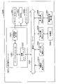
- FIG. 1 is a block diagram showing the configuration of an imaging device according to the first embodiment.
- a plurality of light source cells are arranged two-dimensionally in the light source cell array section 11 .
- Each light source cell emits light based on the light source control signal S ⁇ b>11 from the light source control circuit 12 . This light emission generates an optical signal S12.
- the generated optical signal S ⁇ b>12 is received by the pixel array section 21 .
- a circuit configuration example of the light source cell array section 11 will be described later.
- the light source control circuit 12 has, for example, a drive circuit for driving the light source cell array section 11 and a decoder for selecting a light source cell. to input the light source control signal S11. By this light source control signal S11, the light source control circuit 12 sequentially selects each light source cell of the light source cell array section 11 to emit light, and irradiates the pixel array section 21 with the light signal S12. Note that the light source control circuit 12 may collectively cause the light source cells to emit light.
- the light source logic circuit 13 receives a clock signal input from the outside and data instructing an operation mode, etc., and controls the operation of the light source cell array section 11 as a whole.
- the light source logic circuit 13 may be provided with a memory circuit that holds the coefficients (weights) of the sum-of-products operation.
- a plurality of pixels are arranged two-dimensionally in the pixel array section 21 .
- Each pixel photoelectrically converts the optical signal S12 based on a plurality of types of pixel control signals S21 from the pixel control circuit 22, and generates a pixel signal S22 indicating the result of the sum-of-products operation. Also, each pixel outputs a pixel signal S22 to the pixel signal processing circuit 23 in one direction.
- a circuit configuration example of the pixel array section 21 will be described later.
- the pixel control circuit 22 is composed of, for example, a shift register, and inputs a pixel control signal S21 to each pixel of the pixel array section 21 via pixel drive wiring (not shown in FIG. 1). By this pixel control signal S21, the pixel control circuit 22 sequentially selects and scans each pixel of the pixel array section 21, and outputs the pixel signal S22 to the pixel signal processing circuit . Note that the pixel control circuit 22 may scan each pixel at once.
- the pixel signal processing circuit 23 performs CDS (Correlated Double Sampling) processing for removing pixel-specific fixed pattern noise, AD (Analog to Digital) conversion processing. As a result, the digital pixel signal S ⁇ b>23 is output from the pixel signal processing circuit 23 . Note that the pixel signal processing circuit 23 does not have to perform the CDS processing.
- CDS Correlated Double Sampling
- AD Analog to Digital
- the horizontal driving circuit 24 is composed of, for example, a shift register, and sequentially outputs horizontal scanning pulses to the pixel signal processing circuit 23 .
- the digital pixel signals S23 held in the pixel signal processing circuit 23 are sequentially output.
- the pixel logic circuit 25 receives a clock signal input from the outside and data instructing an operation mode, etc., and controls the operation of the entire pixel array section 21 .
- the pixel logic circuit 25 generates a vertical synchronizing signal, a horizontal synchronizing signal, etc., based on the input clock signal, and supplies them to the pixel control circuit 22 , the pixel signal processing circuit 23 , and the horizontal driving circuit 24 .
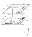
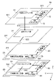
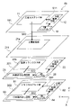
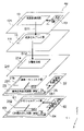
- FIGS. 2A to 2E are diagrams showing an example of the structure of the imaging device 1.
- the light source cell array section 11 , the light source control circuit 12 and the light source logic circuit 13 are arranged on the first substrate 101 .
- the pixel array section 21 , the pixel control circuit 22 , the pixel signal processing circuit 23 and the pixel logic circuit 25 are arranged on the second substrate 201 .
- the horizontal drive circuit 24 is omitted from the second substrate 201 in FIG. 2A for the sake of space.
- FIGS. 2A to 2E two directions parallel to the substrate and perpendicular to each other are defined as the X direction and the Y direction, respectively.
- a direction orthogonal to the X direction and the Y direction, in other words, the stacking direction of the substrates is defined as the Z direction.
- the first substrate 101 and the second substrate 201 are, for example, silicon substrates.
- the two substrates are bonded together, for example, with copper pads, bumps, or TSVs (Through Silicon Via).
- the first substrate 101 and the second substrate 201 do not need to overlap entirely, and at least a portion of the light source cell array section 11 may overlap the pixel array section 21 . If the optical signal S12 of the light source cell array section 11 can be received by a desired pixel in the pixel array section 21, the distance between the first substrate 101 and the second substrate 201 may be several centimeters or they may be close to each other. good.
- the first substrate 101 and the second substrate 201 may be joined by mounting such as solder, for example.
- the distance between the pixel array section 21 and the pixel signal processing circuit 23 is short. Further, the optical center position between the pixel array section 21 and the light source cell array section 11 and the substrate center position between the first substrate 101 and the second substrate 201 may or may not match. .
- the pixel array section 21 can be selected at an optimum position according to specifications.
- the pixel control circuit 22 is arranged in a direction parallel to the output direction of the pixel signal S22, and the pixel signal processing circuit 23 is arranged in a direction perpendicular to the output direction of the pixel signal S22. be. That is, the pixel control circuit 22 and the pixel signal processing circuit 23 are arranged perpendicular to each other. Note that the position of the pixel logic circuit 25 is not limited to the position shown in FIG.
- the plane area of the pixel array section 21 is a rectangle with the X direction as the short side direction and the Y direction as the long side direction, but it may be a square, which is determined according to the specifications of the sum-of-products operation. For example, when the number of convolutions (the number of additions) of the sum-of-products operation is large, a long read wiring is required. In this case, the rectangular pixel array section 21 shown in FIG. 2A is preferable.
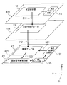
- the light source system has a two-layer structure in which the light source substrate 111 and the light source control substrate 121 are superimposed on each other.
- the light source substrate 111 and the light source control substrate 121 are, for example, silicon substrates.
- the light source substrate 111 is arranged in an intermediate layer between the light source control substrate 121 and the second substrate 201, and the light source control substrate 121 is arranged in the uppermost layer.
- the light source cell array section 11 is arranged on the light source substrate 111 .
- the light source control circuit 12 and the light source logic circuit 13 are arranged on the light source control board 121 .
- the first substrate 101 shown in FIG. 2A or the light source substrate 111 and light source control substrate 121 shown in FIG. 2B each correspond to the first substrate group. That is, the first substrate group may be one substrate or multiple substrates.
- the shutter 102 is provided between the light source cell array section 11 and the pixel array section 21.
- the shutter 102 is opened when the light source cell array section 11 is in the ON state where the optical signal S12 is output, and is closed when the light source cell array section 11 is in the OFF state where no optical signal is output.
- the shutter 102 may be composed of, for example, a mechanical shutter or a liquid crystal shutter.
- the shutter 102 can realize a light blocking function of blocking unnecessary light to the pixel array section 21 when the light source cell array section 11 is turned off.
- a black mask 103 is provided on the edge of the first substrate 101 and the edge of the second substrate 201 .
- the black mask 103 is composed of a light absorber.
- the black mask 103 can block external light entering through the gap between the first substrate 101 and the second substrate 201 .
- the pixel array section 21 can receive only the optical signal S12, thereby improving the calculation accuracy.
- the first substrate 101 and the second substrate 201 are housed in a light-shielding package 104.
- the package 104 is also composed of a light absorber. Like the black mask 103 , the package 104 can block external light entering through the gap between the first substrate 101 and the second substrate 201 . As a result, the pixel array section 21 can receive only the optical signal S12, thereby improving the calculation accuracy.
- FIG. 3A is a cross-sectional view schematically showing the joining form between the light source substrate 111 and the light source control substrate 121 shown in FIG. 2B.
- a plurality of through electrodes 112 formed on the light source substrate 111 and a plurality of connection terminals 122 formed on the light source control substrate 121 are joined.
- the through electrodes 112 and the connection terminals 122 can be made of metal such as copper.
- a gap between the light source substrate 111 and the light source control substrate 121 is filled with an insulating film.
- the through electrodes 112 pass through the light source substrate 111 and are electrically connected to the light source cell array section 11 via a wiring layer (not shown) including various wirings.
- the connection terminals 122 are formed on the surface of the light source control board 121 (the joint surface with the light source board 111).
- the connection terminals 122 are connected to the light source control circuit 12 and the light source logic circuit 13 arranged on the light source control board 121 via various wiring layers (not shown).
- the light source control signal S11 of the light source control circuit 12 is transmitted from the connection terminal 122 to each light source of the light source cell array section 11 through the through electrodes 112 .
- FIG. 3B is a cross-sectional view schematically showing another joining form between the light source substrate 111 and the light source control substrate 121.
- the joining form shown in FIG. 3B is a so-called Cu--Cu joining in which a plurality of connection terminals 113 formed on the light source substrate 111 and a plurality of connection terminals 122 formed on the light source control substrate 121 are joined.
- the connection terminals 113 can be made of a metal such as copper, like the connection terminals 122, and are electrically connected to the light source cell array section 11 via wiring (not shown). Note that, even in this bonding mode, the gap between the light source substrate 111 and the light source control substrate 121 is filled with an insulating film.
- the light source control signal S11 of the light source control circuit 12 is transmitted from the connection terminal 122 to each light source of the light source cell array section 11 through the connection terminal 113 .
- the light source cell array section 11 is formed above the through electrodes 112 or the connection terminals 113 . Also, the light source control circuit 12 and the light source logic circuit 13 are formed in a layer above the connection terminals 122 .
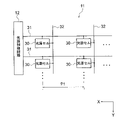
- FIG. 4A is a diagram showing a schematic configuration of the light source cell array section 11.
- FIG. 4A a plurality of light source cells 30 are arranged two-dimensionally in the light source cell array section 11 .
- Each light source cell 30 is arranged near an intersection point between a light source driving wiring 31 and a light source driving wiring 32 orthogonal to the light source driving wiring 31 .
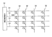
- FIG. 4B is a diagram showing an example of the light source cell 30.
- the light source cell 30 is composed of light emitting elements 300 .
- the anode is connected to the light source driving wiring 31 and the cathode is connected to the light source driving wiring 32 .
- an LED Light Emitting Diode
- an SLED Super Light Emitting Diode
- an OLED Organic Light Emitting Diode
- a laser VCSEL
- Each light emitting element 300 emits light in response to a light source control signal S11 input from the light source control circuit 12 through the light source drive wiring 31 to generate an optical signal S12.
- the light source cell array section 11 shown in FIG. 4B is driven by a passive matrix system that controls each light emitting element 300 in a time division manner.
- the light of each light emitting element 300 that is, the wavelength of the optical signal S12 may be different for each light source cell 30, or may be the same for all the light source cells 30.
- the wavelength of the optical signal S12 may be within the range from infrared rays to visible light, but a long wavelength is preferable.
- the wavelength of the optical signal S ⁇ b>12 may be selected according to the light receiving range of the pixel array section 21 .
- FIG. 4C is a diagram showing another example of the light source cell 30.
- FIG. This light source cell 30 is provided with an active element 310 in addition to the light emitting element 300 .
- the active element 310 is composed of, for example, an N-channel MOS (Metal Oxide Semiconductor) transistor, as shown in FIG. 4C.
- MOS Metal Oxide Semiconductor
- the gate is connected to the light source driving wiring 31
- the drain is connected to the light emitting element 300
- the source is connected to the light source driving wiring 32 .
- the light source cell array section 11 in FIG. 4C is driven by an active matrix system in which the active elements 310 control the light emitting elements 300 independently of other light emitting elements 300 .
- the light of each light emitting element 300 that is, the wavelength of the optical signal S12 may be different for each light source cell 30, or may be the same for all the light source cells 30.
- the wavelength of the optical signal S12 may be within the range from infrared rays to visible light, but a long wavelength is preferable.
- the wavelength of the optical signal S ⁇ b>12 may be selected according to the light receiving range of the pixel array section 21 .
- FIG. 4D is a diagram showing still another example of the light source cell 30.
- FIG. A storage section 320 is provided between the light emitting element 300 and the active element 310 in the light source cell 30 .
- SRAM Static Random Access Memory
- a latch circuit a flip-flop, a non-volatile memory, and the like can be applied to the storage unit 320 .
- each memory when a voltage is applied between the light source driving wiring 31 and the light source driving wiring 32, that is, when the light source control signal S11 is input to each light source cell 30 through the light source driving wiring 31, each memory The voltage applied to each light emitting element 300 is determined according to the state of the portion 320 .
- This applied voltage corresponds to the coefficient of the sum-of-products operation of the pixel array section 21 . That is, the storage unit 320 stores data regarding the coefficients of the sum-of-products operation. This data may be stored in multiple bits. In addition, this data may contain other information besides the coefficients of the sum-of-products operation.
- the configuration of the light source cell 30 is not limited to the configurations shown in FIGS. 4B, 4C, and 4D.
- the light source cell 30 may have, for example, a transmissive or reflective liquid crystal module or electronic paper in addition to the light emitting element 300 .
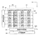
- FIG. 5A is a diagram showing a schematic configuration of the pixel array section 21.
- FIG. 5A in the pixel array section 21, a plurality of pixels 50 are arranged between the pixel drive wiring 41 connected to the pixel control circuit 22 and the pixel readout wiring 42 connected to the pixel signal processing circuit 23. They are arranged two-dimensionally.
- the center pitch P1 of the light source cells 30 shown in FIG. 4A is an integer multiple of the center pitch P2 of the pixels 50. There may be. That is, in the light source cells 30 and the pixels 50, the center pitch of one is an integral multiple of the center pitch of the other. In other words, in the light source cells 30 and the pixels 50, one number is an integral multiple of the other number.
- Each pixel 50 generates a photoelectric conversion signal of the optical signal S12 according to the pixel control signal S21 input through the pixel drive wiring 41.
- the signal value of the pixel control signal S21 is multiplied by the amount of light of the optical signal S12 and the exposure time, that is, the amount of charge received by the pixel 50 as a coefficient.
- the pixel array unit 21 sequentially adds the multiplication results in units of rows or columns through the pixel readout wirings 42 .
- an analog pixel signal S ⁇ b>22 indicating the sum-of-products operation result is read out to the pixel signal processing circuit 23 .
- the sum-of-products operation is performed in an analog manner, digital processing is unnecessary. Therefore, the power consumed by the sum-of-products operation is reduced.
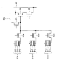
- 5B to 5F are diagrams showing examples of equivalent circuit diagrams of the pixel 50.
- FIG. The circuit configuration of the pixel shown in each drawing will be described below.
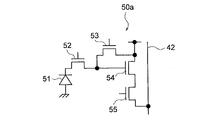
- a pixel 50 a shown in FIG. 5B has a photodiode 51 , a transfer transistor 52 , a reset transistor 53 , an amplification transistor 54 and a selection transistor 55 .
- the photodiode 51 generates and accumulates charges (signal charges) corresponding to the light intensity of the optical signal S12.
- the photodiode 51 has an anode terminal grounded and a cathode terminal connected to the transfer transistor 52 .
- the transfer transistor 52 When the transfer transistor 52 is turned on by a transfer signal from the pixel control circuit 22 , the charge is read from the photodiode 51 and transferred to the amplification transistor 54 .
- the reset transistor 53 When the reset transistor 53 is turned on by a reset signal from the pixel control circuit 22 , the charge accumulated in the photodiode 51 is discharged to the power supply, thereby resetting the potential of the photodiode 51 .
- the amplification transistor 54 outputs a pixel signal S22 corresponding to the amount of charge accumulated in the photodiode 51 to the selection transistor 55 .
- the selection transistor 55 outputs the pixel signal S22 to the pixel readout line 42 when turned on by a selection signal that is one of the pixel control signals S21.
- the pixel signal S22 is transmitted to the pixel signal processing circuit 23 via the pixel readout wiring 42 .
- a pixel 50b shown in FIG. 5C has two photodiodes 51a and 51b. Charges generated by photoelectric conversion of photodiode 51a are temporarily held in memory transistor 57a and capacitor 58a. The held charges are transferred to the amplification transistor 54 by the transfer transistor 52a. On the other hand, charges generated by photoelectric conversion of the photodiode 51b are temporarily held in the memory transistor 57b and the capacitor 58b. The retained charges are transferred to the amplification transistor 54 by the transfer transistor 52b.
- the amplification transistor 54 outputs to the selection transistor 55 a pixel signal S22 corresponding to the amount of charge transferred from the transfer transistor 52a or the transfer transistor 52b.
- the selection transistor 55 outputs the pixel signal S22 to the pixel readout line 42 .
- the pixel signal S22 is transmitted to the pixel signal processing circuit 23 via the pixel readout wiring 42 .
- a reset transistor 53 resets the potential of each of the photodiodes 51a and 51b.
- a pixel 50c shown in FIG. 5D is an example of a so-called PWM (Pulse Wide Modulation) pixel.
- the slope signal S11a which is one of the pixel control signals S21, is input to the gate of the P-channel MOS transistor 59 in the pixel 50b.
- the MOS transistor 59 is connected in series with the amplification transistor 54 .
- the selection transistor 55 outputs a PWM pixel signal S22 indicating the comparison result between the output of the MOS transistor 59 and the output of the amplification transistor 54 to the pixel readout line 42 .
- the pixel signal S22 is transmitted to the pixel signal processing circuit 23 via the pixel readout wiring 42 .
- the photodiodes 51a to 51c each have a photoelectric conversion film 511, a transparent electrode 512, and a lower electrode 513.
- the photoelectric conversion film 511 is an organic photoelectric conversion film or an inorganic photoelectric conversion film.
- the transparent electrode 512 is arranged on the upper surface of the photoelectric conversion film 511 .
- the lower electrode 513 is arranged on the upper surface of the photoelectric conversion film 511 . That is, the transparent electrode 512 is sandwiched between the transparent electrode 512 and the lower electrode 513 .
- the photoelectric conversion film 511 controls the voltage of the transparent electrode 512 to realize a global shutter.
- the charges photoelectrically converted by the photoelectric conversion films 511 of the photodiodes 51a to 51c are transferred to the amplification transistors 54 by the transfer transistors 52a to 52c, respectively.
- the amplification transistor 54 outputs a pixel signal S22 corresponding to the charge amount accumulated in the photodiode 51 to the selection transistor 55 .
- the selection transistor 55 outputs the pixel signal S22 to the pixel readout line 42 .
- the pixel signal S22 is transmitted to the pixel signal processing circuit 23 via the pixel readout wiring 42 .
- the potential of each photodiode is reset by a reset transistor 53 .
- a pixel 50e shown in FIG. 5F is an example of a DVS (Dynamic Vision Sensor) pixel that outputs changes in brightness.
- Pixel 50 e has logarithmic conversion circuitry 510 , buffer circuitry 520 , subtraction circuitry 530 and quantization circuitry 540 .
- the logarithmic conversion circuit 510 has a photodiode 51 , an N-channel MOS transistor 514 , a P-channel MOS transistor 515 , and an N-channel MOS transistor 516 .
- Photodiode 51 and MOS transistor 514 are connected in series.
- MOS transistors 515 and 516 are also connected in series.
- the gate of MOS transistor 514 is connected to the drain of MOS transistor 515 and the drain of MOS transistor 516 .
- the logarithmic conversion circuit 510 converts the charge photoelectrically converted by the photodiode 51 into a logarithmic output voltage Vlog.
- the buffer circuit 520 has a P-channel MOS transistor 521 and a P-channel MOS transistor 522 . MOS transistor 521 and MOS transistor 522 are connected in series. Buffer circuit 520 outputs a source follower voltage VSF obtained by performing impedance conversion on voltage Vlog input to the gate of MOS transistor 522 .
- the subtraction circuit 530 has a P-channel MOS transistor 531 , a P-channel MOS transistor 532 , an N-channel MOS transistor 533 , a capacitor 534 and a capacitor 535 .
- MOS transistor 532 and MOS transistor 533 are connected in series.
- a capacitor 534 is connected to the gate of the MOS transistor 532 .
- MOS transistor 531 and capacitor 535 are connected in parallel between the gate and drain of MOS transistor 532 .
- Subtraction circuit 530 outputs a differential voltage Vdiff from the previous signal.
- the quantization circuit 540 has a P-channel MOS transistor 541 , an N-channel MOS transistor 542 , a P-channel MOS transistor 543 , and an N-channel MOS transistor 544 .
- MOS transistor 541 and MOS transistor 542 are connected in series.
- MOS transistors 543 and 544 are also connected in series.
- Quantization circuit 540 compares differential voltage Vdiff input to the gates of MOS transistors 541 and 543 with two threshold values. After that, the comparison result (VO(+), VO(-)) is transmitted to the pixel signal processing circuit 23 via the pixel readout wiring 42 as the pixel signal S22.
- the pixel signal processing circuit 23 determines "+1", "0" and "-1" based on the pixel signal S22.
- the pixels 50 arranged in the pixel array section 21 are not limited to the pixels 50a to 50e shown in FIGS. 5B to 5F.
- so-called convolution pixels that add the pixel signals S22 of the pixels 50 may be arranged.
- a polarization sensor or a multispectral sensor may be arranged in the pixel array section 21 .
- the polarization sensor further has a diffraction element that polarizes the light incident on the photodiode 51 .
- the multispectral sensor further has a color filter that color separates the light incident on the photodiode 51 .
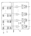
- FIG. 6 is a diagram showing an example of the circuit configuration of an ADC (Analog to Digital Converter) included in the pixel signal processing circuit 23.
- ADC Analog to Digital Converter
- FIG. 6 has multiple comparators 231 , multiple counters 232 , and multiple latch circuits 233 .
- the non-inverting input terminal of the comparator 231 receives the pixel signal S22 of the pixel 50 corresponding to one of the pixels 50a to 50e described above.
- a triangular wave ramp signal RAMP is input to the inverting input terminal.
- Each comparator 231 outputs a comparison result between the pixel signal S22 and the ramp signal RAMP.
- Each counter 232 is connected to the output terminal of the comparator 231 .
- Each counter 232 counts the change time of the output level of the comparator 231 .
- Each latch circuit 233 holds the count result of each counter 232 .
- the ADC included in the pixel signal processing circuit 23 is not limited to the single slope ADC shown in FIG.
- the pixel signal processing circuit 23 includes, for example, a pixel ADC that processes the pixel signal S22 for each pixel, a column ADC that counts comparison times of a plurality of comparators 231 with one counter 232, a double integration type ADC that has an integration circuit, a sequential A comparison type (SAR) ADC, a delta-sigma type ADC, or the like may be included.
- the resolution of the ADC can be appropriately selected within the range of 1 bit to 12 bits, for example.
- the imaging device 1 has a configuration in which the pixel array section 21 performs a sum-of-products operation on the optical signal S12 generated by the light source cell array section 11 .
- the coefficient (weight) data necessary for the sum-of-products calculation is transferred to the plurality of pixels 50 arranged two-dimensionally, so the power required for data transfer is greatly reduced. .
- the sum-of-products operation is performed.
- coefficient data can be set freely. As a result, it is possible to expand the expression width of the sum-of-products operation.
- the present embodiment described above it is possible to expand the expressive power of coefficients during calculations with low latency, so advanced calculations can be realized with low power. In particular, it can be expected to contribute to improving the efficiency of large-scale operations used in data centers and the like. Further, in this embodiment, the light source cell array section 11 is laminated on the pixel array section 21, so a small area layout can be realized. Furthermore, since the present disclosure can use a CMOS image sensor as a sum-of-products operator, it can also benefit from technological advances in CMOS image sensors.
- FIG. 7 is a block diagram showing the configuration of an imaging device according to the second embodiment. Components similar to those of the first embodiment are denoted by the same reference numerals, and detailed description thereof is omitted.
- the imaging device 2 shown in FIG. 7 includes a memory cell array section 61, a CIM (Computing in memory) input control circuit 62, a CIM reading circuit 63, and a CIM logic circuit 64 in addition to the components of the imaging device 1 shown in FIG. Prepare more.
- a CIM Computer in memory
- a plurality of memory cells are arranged two-dimensionally in the memory cell array section 61 .
- the memory cell array section 61 unidirectionally outputs a convolution signal S62 indicating the result of analog sum-of-products operation of the memory cell control signal S61 from the CIM input control circuit 62 to the CIM reading circuit 63 .
- a circuit configuration example of the memory cell array section 61 will be described later.
- the CIM input control circuit 62 is composed of, for example, a shift register, and outputs a memory cell control signal associated with the digital pixel signal S23 to each memory cell of the memory cell array section 61 via memory cell drive wiring (not shown in FIG. 7). Enter S61. In accordance with this memory cell control signal S61, the CIM input control circuit 62 selects and scans each memory cell of the memory cell array section 61 sequentially or collectively, and performs a sum-of-products operation using the memory value of each memory cell to generate a convolution signal S62. is output to the CIM reading circuit 63 .
- the CIM reading circuit 63 performs AD conversion processing and the like on the convolution signal S62 read from the memory cell array section 61.
- the CIM logic circuit 64 receives a clock signal input from the outside and data instructing the operation mode, etc., and controls the operation of the entire memory cell array section 61 .
- the CIM logic circuit 64 generates a vertical synchronizing signal, a horizontal synchronizing signal, etc., based on the input clock signal, and supplies them to the CIM input control circuit 62 and the CIM reading circuit 63 .
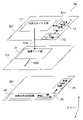
- FIG. 8A is a diagram showing an example of the structure of the imaging device 2.
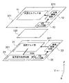
- the first substrate 101, the second substrate 201, and the memory substrate 202 are laminated in this order.
- the first substrate 101 is arranged on the top layer
- the memory substrate 202 is arranged on the bottom layer
- the second substrate 201 is arranged on the intermediate layer between the first substrate 101 and the memory substrate 202 .
- a light source cell array section 11, a light source control circuit 12, and a light source logic circuit 13 are arranged on the first substrate 101, as in FIG. 2A.
- a pixel array section 21, a pixel control circuit 22, a pixel signal processing circuit 23, and a pixel logic circuit 25 are arranged on the second substrate 201, as in FIG. 2A.
- a memory substrate 202 is stacked under the second substrate 201 .
- the memory substrate 202 is, for example, a silicon substrate, and is bonded to the second substrate 201 by copper pads, bumps, TSVs, or the like.
- the memory substrate 202 constitutes a second substrate group together with the second substrate 201 . In order to minimize the substrate area, the memory substrate 202 need not entirely overlap the second substrate 201, but only partially overlap each other.
- a memory cell array section 61 , a CIM input control circuit 62 , a CIM read circuit 63 and a CIM logic circuit 64 are arranged on the memory substrate 202 .
- CIM input control circuit 62 is arranged in a direction parallel to the output direction of convolved signal S62
- CIM readout circuit 63 is arranged in a direction perpendicular to the output direction of convolved signal S62. That is, the CIM input control circuit 62 and the CIM readout circuit 63 are arranged perpendicular to each other.
- the position of the CIM logic circuit 64 is not limited to the position shown in FIG.
- the plane area of the memory cell array section 61 is a rectangle with the short side in the X direction and the long side in the Y direction. It is determined. For example, when the number of convolutions (the number of additions) of the sum-of-products operation is large, a long read wiring is required. In this case, the rectangular shape of the memory cell array section 61 shown in FIG. 8A is preferable.
- FIG. 8B is a diagram showing another example of the structure of the imaging device 2.
- the light source system similarly to FIG. 2B, the light source system has a two-layer structure in which the light source substrate 111 and the light source control substrate 121 are stacked one on top of the other.
- the light source cell array section 11 is arranged on the light source control board 121 .
- the light source control circuit 12 and the light source logic circuit 13 are arranged on the light source control board 121 .
- the shutter 102 may also be provided between the light source cell array section 11 and the pixel array section 21 in the imaging device 2 according to the present embodiment, as in the first embodiment.
- a black mask 103 may be provided on the edge of the first substrate 101 and the edge of the second substrate 201 .
- the imaging device 2 may be housed in a light-shielding package 104 (see FIG. 2E).
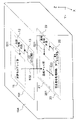
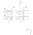
- FIG. 9 is a diagram showing a schematic circuit configuration of the memory cell array section 61.
- a plurality of memory cells 71 are arranged two-dimensionally.
- Each memory cell 71 is arranged near the intersection of the memory cell drive wiring 72 and the memory cell readout wiring 73 .
- the memory cells 71 may be arranged three-dimensionally. In this case, multiple memory cells 71 are arranged in the X, Y, and Z directions.
- the memory cell 71 includes, for example, a resistance change memory (ReRAM: Resistive Random Access Memory), a phase change memory (PCM: Phase Change Memory), a magnetoresistive memory (MRAM: Magneto resistive Random Memory), or a ferroelectric memory ( FeRAM: Ferroelectric Random Access Memory) can be applied. Also, the memory cell 71 may be an SRAM (Static Random Access Memory) or a non-volatile memory.
- ReRAM Resistive Random Access Memory
- PCM Phase Change Memory
- MRAM Magnetoresistive memory
- FeRAM Ferroelectric Random Access Memory
- the memory cells 71 hold memory values (eg, +1, -1, 0.5).
- the memory cell array section 61 multiplies the memory value of each memory cell 71 by the signal value of the memory cell control signal S61 input as an input signal from the CIM input control circuit 62 via the memory cell drive wiring 72 . Subsequently, the memory cell array section 61 sequentially adds the multiplication results in units of rows or columns through the memory cell readout wirings 73 . As a result, a digital convolution signal S62 indicating the sum-of-products operation result is read out to the CIM reading circuit 63. FIG. Note that the memory cell array unit 61 may collectively add the multiplication results.
- the convolution signal S62 is of analog type, after the input signal through the memory cell drive wiring 72 and the memory value are multiplied, the charge is added on the memory cell readout wiring 73, and the convolution signal S62 is output to the CIM readout circuit. 63. At this time, the input signal can be input to all the memory cell drive wirings 72 at once, and when the CIM readout circuit 63 is a column ADC, the convolution signal S62 can be read out from all the memory cell readout wirings 73 at once. is also possible.
- the imaging device 2 according to the present embodiment described above also has a configuration in which the pixel array section 21 performs a sum-of-products operation on the optical signal S12 generated by the light source cell array section 11, as in the first embodiment. Therefore, advanced computation can be realized with low power. Furthermore, the imaging device 2 according to the present embodiment also includes a memory cell array section 61 that performs a sum-of-products operation on the calculation result of the pixel array section 21 . Therefore, it is also possible to perform more advanced calculations.
- FIGS. 10A to 10D are diagrams showing the structure of an imaging device according to the third embodiment. Components similar to those in the above-described embodiment are denoted by the same reference numerals, and detailed descriptions thereof are omitted.
- the optical system has a single-layer structure in which all the circuit elements are arranged on the first substrate 101, whereas the pixel system has a pixel substrate 211 and a pixel control substrate 221 which overlap each other. It is a combined two-layer structure.
- the pixel substrate 211 and pixel control substrate 221 are, for example, silicon substrates.
- the pixel substrate 211 is arranged in an intermediate layer between the first substrate 101 and the pixel control substrate 221, and the pixel control substrate 221 is arranged in the bottom layer.
- the pixel array section 21 is arranged on the pixel substrate 211 .
- any of the pixels 50a (see FIG. 5B), the pixels 50b (see FIG. 5C), or the pixels 50d (see FIG. 5E) described in the first embodiment are arranged two-dimensionally. be.
- the pixel control circuit 22, the pixel signal processing circuit 23, and the pixel logic circuit 25 are arranged on the pixel control board 221.
- the second substrate 201 shown in FIG. 2A or the pixel substrate 211 and pixel control substrate 221 shown in FIG. 10B each correspond to the second substrate group. That is, the second substrate group may be one substrate or multiple substrates.
- the pixel substrate 211 and the pixel control substrate 221 are joined via through electrodes or connection terminals, like the light source substrate 111 and the light source control substrate 121 .
- the pixel control signal S21 and the pixel signal S22 are transmitted through through electrodes or connection terminals.
- the pixel array section 21 is dispersedly arranged on the pixel substrate 211 and the pixel control substrate 221.
- the pixel substrate 211 is provided with a photoelectric conversion unit 21a that photoelectrically converts the optical signal S12
- the pixel control substrate 221 is provided with a pixel transistor unit 21b that performs a sum-of-products operation on the optical signal S12.
- the pixels 50c see FIG. 5D
- the pixels 50e see FIG. 5F
- the photodiode 51 and the amplification transistor 54 are arranged on the pixel substrate 211 as the photoelectric conversion section 21a.
- a reset transistor 53, a selection transistor 55, and a MOS transistor 59 are arranged on the pixel control substrate 221 as the pixel transistor section 21b.
- the logarithmic conversion circuit 510 is arranged on the pixel substrate 211 as the photoelectric conversion section 21a.
- a buffer circuit 520, a subtraction circuit 530, and a quantization circuit 540 are arranged on the pixel control board 221 as the pixel transistor section 21b.
- both the optical system and the pixels have a two-layer structure.
- the light source cell array section 11 is arranged on the light source substrate 111
- the light source control circuit 12 and the light source logic circuit 13 are arranged on the light source control substrate 121 .
- the pixel array section 21 is arranged on the pixel substrate 211
- the pixel control circuit 22, the pixel signal processing circuit 23, and the pixel logic circuit 25 are arranged on the pixel control substrate 221, as in FIG. 10A. .
- both the optical system and the pixels have a two-layer structure.
- the photoelectric conversion portion 21a of the pixel array portion 21 is arranged on the pixel substrate 211, and the pixel transistor portion 21b is arranged on the pixel control substrate 221, as in FIG. 10B.
- the imaging device 3 according to the present embodiment described above also has a configuration in which the pixel array section 21 performs a sum-of-products operation on the optical signal S12 generated by the light source cell array section 11, as in the first embodiment. Therefore, advanced computation can be realized with low power. Furthermore, in this embodiment, the pixel system has a two-layer structure. Therefore, the arrangement area of the pixel array section 21, that is, the sum-of-products operation area can be enlarged. This also makes it possible to perform more advanced calculations.
- the imaging device 3 may also be provided with the shutter 102 (see FIG. 2C) and the black mask 103 (see FIG. 2D) as in the first embodiment. Further, the imaging device 3 may be housed in a light-shielding package 104 (see FIG. 2E).
- FIGS. 11A to 11D are diagrams showing the structure of an imaging device according to the fourth embodiment. Components similar to those in the above-described embodiment are denoted by the same reference numerals, and detailed descriptions thereof are omitted.
- the memory substrate 202 is arranged below the pixel control substrate 221 of the imaging device 3a (see FIG. 10A) according to the above-described third embodiment.
- a memory cell array section 61, a CIM input control circuit 62, a CIM read circuit 63, and a CIM logic circuit 64 are arranged on the memory substrate 202, as in the second embodiment.
- the memory substrate 202 is arranged below the pixel control substrate 221 of the imaging device 3b (see FIG. 10B) according to the above-described third embodiment.
- a memory cell array section 61, a CIM input control circuit 62, a CIM read circuit 63, and a CIM logic circuit 64 are arranged on the memory substrate 202, as in the second embodiment.
- the memory substrate 202 is arranged below the pixel control substrate 221 of the imaging device 3c (see FIG. 10C) according to the above-described third embodiment.
- a memory cell array section 61, a CIM input control circuit 62, a CIM read circuit 63, and a CIM logic circuit 64 are arranged on the memory substrate 202, as in the second embodiment.
- the memory substrate 202 is arranged below the pixel control substrate 221 of the imaging device 3d (see FIG. 10D) according to the above-described third embodiment.
- a memory cell array section 61, a CIM input control circuit 62, a CIM read circuit 63, and a CIM logic circuit 64 are arranged on the memory substrate 202, as in the second embodiment.
- the imaging device 4 according to the present embodiment described above also has a configuration in which the pixel array section 21 performs a sum-of-products operation on the optical signal S12 generated by the light source cell array section 11, as in the first embodiment. Therefore, advanced computation can be realized with low power. Furthermore, the imaging device 4 according to the present embodiment also includes a memory cell array section 61 that further performs a sum-of-products operation on the calculation result of the pixel array section 21, as in the second embodiment. Therefore, it is also possible to perform more advanced calculations.
- FIG. 12 is a diagram showing the structure of an imaging device according to the fifth embodiment.
- the same reference numerals are assigned to the same components as in the above-described embodiment, and detailed description thereof will be omitted.
- the optical modulation element 401 is provided between the light source cell array section 11 and the pixel array section 21 .
- a plurality of optical signals S12 incident from the light source cell array section 11 interfere with each other. Due to this interference, the sum-of-products operation is performed not only in the pixel array section 21 but also in the light area.
- the optical modulation element 401 by arranging the optical modulation element 401 between the light source cell array section 11 and the pixel array section 21, it is possible to additionally perform the sum-of-products operation in the light region. Therefore, it is possible to perform a more advanced sum-of-products operation.
- the optical modulation element 401 may be provided between the light source cell array section 11 and the pixel array section 21.
- FIG. 13 is a diagram showing the structure of an imaging device according to the sixth embodiment.
- the same reference numerals are assigned to the same components as in the above-described embodiment, and detailed description thereof will be omitted.
- the reflected light S31 reflected by the subject is incident on the pixel array section 21 in addition to the optical signal S12.
- the optical signal S12 is incident from the light source cell array section 11 arranged above the pixel array section 21 .
- the reflected light S31 is incident from the opposite direction to the optical signal S12, that is, from below the pixel array section 21 .
- the pixel array unit 21 When the pixel array unit 21 receives the optical signal S12, it performs a sum-of-products operation based on the optical signal S12, and outputs the pixel signal S22 to the pixel signal processing circuit . Further, when receiving the reflected light S31, the pixel array section 21 outputs to the pixel signal processing circuit 23 a pixel signal S32 obtained by photoelectrically converting the reflected light S31. In this case, the image signal of the object is generated in the pixel signal processing circuit 23 .
- FIG. 14 is a diagram illustrating an example of the configuration of an electronic device according to the seventh embodiment.
- the electronic device 200 according to this embodiment is a camera system, and as shown in FIG. .
- the lens 220 forms an image of incident light (image light) on the imaging surface.
- the drive circuit 230 has a timing generator (not shown) that generates various timing signals including start pulses and clock pulses for driving circuits in the imaging device 210, and drives the imaging device 210 with predetermined timing signals.
- the signal processing circuit 240 performs predetermined signal processing on the output signal of the imaging device 210 .
- the image signal processed by the signal processing circuit 240 is recorded in a recording medium such as a memory. Image information recorded on a recording medium is hard-copied by a printer or the like. Also, the image signal processed by the signal processing circuit 240 is displayed as a moving image on a monitor such as a liquid crystal display.
- the imaging device according to each of the embodiments described above as the imaging device 210 in the electronic device 200 such as a digital still camera, a highly accurate imaging function can be realized.
- the technology (the present technology) according to the present disclosure can be applied to various products.
- the technology according to the present disclosure can be realized as a device mounted on any type of moving body such as automobiles, electric vehicles, hybrid electric vehicles, motorcycles, bicycles, personal mobility, airplanes, drones, ships, and robots. may
- FIG. 15 is a block diagram showing a schematic configuration example of a vehicle control system, which is an example of a mobile control system to which the technology according to the present disclosure can be applied.
- a vehicle control system 12000 includes a plurality of electronic control units connected via a communication network 12001.
- vehicle control system 12000 includes drive system control unit 12010 , body system control unit 12020 , vehicle exterior information detection unit 12030 , vehicle interior information detection unit 12040 , and integrated control unit 12050 .
- a microcomputer 12051 , an audio/image output unit 12052 , and an in-vehicle network I/F (Interface) 12053 are illustrated as the functional configuration of the integrated control unit 12050 .
- the drive system control unit 12010 controls the operation of devices related to the drive system of the vehicle according to various programs.
- the driving system control unit 12010 includes a driving force generator for generating driving force of the vehicle such as an internal combustion engine or a driving motor, a driving force transmission mechanism for transmitting the driving force to the wheels, and a steering angle of the vehicle. It functions as a control device such as a steering mechanism to adjust and a brake device to generate braking force of the vehicle.
- the body system control unit 12020 controls the operation of various devices equipped on the vehicle body according to various programs.
- the body system control unit 12020 functions as a keyless entry system, a smart key system, a power window device, or a control device for various lamps such as headlamps, back lamps, brake lamps, winkers or fog lamps.
- the body system control unit 12020 can receive radio waves transmitted from a portable device that substitutes for a key or signals from various switches.
- the body system control unit 12020 receives the input of these radio waves or signals and controls the door lock device, power window device, lamps, etc. of the vehicle.
- the vehicle exterior information detection unit 12030 detects information outside the vehicle in which the vehicle control system 12000 is installed.
- the vehicle exterior information detection unit 12030 is connected with an imaging section 12031 .
- the vehicle exterior information detection unit 12030 causes the imaging unit 12031 to capture an image of the exterior of the vehicle, and receives the captured image.
- the vehicle exterior information detection unit 12030 may perform object detection processing or distance detection processing such as people, vehicles, obstacles, signs, or characters on the road surface based on the received image.
- the imaging unit 12031 is an optical sensor that receives light and outputs an electrical signal according to the amount of received light.
- the imaging unit 12031 can output the electric signal as an image, and can also output it as distance measurement information.
- the light received by the imaging unit 12031 may be visible light or non-visible light such as infrared rays.
- the in-vehicle information detection unit 12040 detects in-vehicle information.
- the in-vehicle information detection unit 12040 is connected to, for example, a driver state detection section 12041 that detects the state of the driver.
- the driver state detection unit 12041 includes, for example, a camera that captures an image of the driver, and the in-vehicle information detection unit 12040 detects the degree of fatigue or concentration of the driver based on the detection information input from the driver state detection unit 12041. It may be calculated, or it may be determined whether the driver is dozing off.
- the microcomputer 12051 calculates control target values for the driving force generator, the steering mechanism, or the braking device based on the information inside and outside the vehicle acquired by the vehicle exterior information detection unit 12030 or the vehicle interior information detection unit 12040, and controls the drive system control unit.
- a control command can be output to 12010 .
- the microcomputer 12051 realizes the functions of ADAS (Advanced Driver Assistance System) including collision avoidance or shock mitigation of vehicles, follow-up driving based on inter-vehicle distance, vehicle speed maintenance driving, vehicle collision warning, vehicle lane deviation warning, etc. Cooperative control can be performed for the purpose of ADAS (Advanced Driver Assistance System) including collision avoidance or shock mitigation of vehicles, follow-up driving based on inter-vehicle distance, vehicle speed maintenance driving, vehicle collision warning, vehicle lane deviation warning, etc. Cooperative control can be performed for the purpose of ADAS (Advanced Driver Assistance System) including collision avoidance or shock mitigation of vehicles, follow-up driving based on inter-vehicle distance, vehicle speed maintenance driving
- the microcomputer 12051 controls the driving force generator, the steering mechanism, the braking device, etc. based on the information about the vehicle surroundings acquired by the vehicle exterior information detection unit 12030 or the vehicle interior information detection unit 12040, so that the driver's Cooperative control can be performed for the purpose of autonomous driving, etc., in which vehicles autonomously travel without depending on operation.
- the microcomputer 12051 can output a control command to the body system control unit 12030 based on the information outside the vehicle acquired by the information detection unit 12030 outside the vehicle.
- the microcomputer 12051 controls the headlamps according to the position of the preceding vehicle or the oncoming vehicle detected by the vehicle exterior information detection unit 12030, and performs cooperative control aimed at anti-glare such as switching from high beam to low beam. It can be carried out.
- the audio/image output unit 12052 transmits at least one of audio and/or image output signals to an output device capable of visually or audibly notifying the passengers of the vehicle or the outside of the vehicle.
- an audio speaker 12061, a display section 12062 and an instrument panel 12063 are illustrated as output devices.
- the display unit 12062 may include at least one of an on-board display and a head-up display, for example.
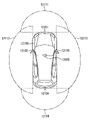
- FIG. 16 is a diagram showing an example of the installation position of the imaging unit 12031.
- the imaging unit 12031 has imaging units 12101, 12102, 12103, 12104, and 12105.
- the imaging units 12101, 12102, 12103, 12104, and 12105 are provided at positions such as the front nose, side mirrors, rear bumper, back door, and windshield of the vehicle 12100, for example.
- An image pickup unit 12101 provided in the front nose and an image pickup unit 12105 provided above the windshield in the passenger compartment mainly acquire an image in front of the vehicle 12100 .
- Imaging units 12102 and 12103 provided in the side mirrors mainly acquire side images of the vehicle 12100 .
- An imaging unit 12104 provided in the rear bumper or back door mainly acquires an image behind the vehicle 12100 .
- the imaging unit 12105 provided above the windshield in the passenger compartment is mainly used to detect preceding vehicles, pedestrians, obstacles, traffic lights, traffic signs, lanes, and the like.
- FIG. 16 shows an example of the imaging range of the imaging units 12101 to 12104.
- the imaging range 12111 indicates the imaging range of the imaging unit 12101 provided on the front nose
- the imaging range 1211212113 indicates the imaging ranges of the imaging units 12102 and 12103 provided on the side mirrors
- the imaging range 12114 indicates the imaging range of the rear bumper or
- the imaging range of the imaging unit 12104 provided in the back door is shown. For example, by superimposing the image data captured by the imaging units 12101 to 12104, a bird's-eye view image of the vehicle 12100 viewed from above can be obtained.
- At least one of the imaging units 12101 to 12104 may have a function of acquiring distance information.
- at least one of the imaging units 12101 to 12104 may be a stereo camera composed of a plurality of imaging elements, or may be an imaging element having pixels for phase difference detection.
- the microcomputer 12051 determines the distance to each three-dimensional object within the imaging ranges 12111 to 12114 and changes in this distance over time (relative velocity with respect to the vehicle 12100). , it is possible to extract, as the preceding vehicle, the closest three-dimensional object on the traveling path of the vehicle 12100, which runs at a predetermined speed (for example, 0 km/h or more) in substantially the same direction as the vehicle 12100. can. Furthermore, the microcomputer 12051 can set the inter-vehicle distance to be secured in advance in front of the preceding vehicle, and perform automatic brake control (including following stop control) and automatic acceleration control (including following start control). In this way, cooperative control can be performed for the purpose of automatic driving in which the vehicle runs autonomously without relying on the operation of the driver.
- automatic brake control including following stop control
- automatic acceleration control including following start control
- the microcomputer 12051 converts three-dimensional object data related to three-dimensional objects to other three-dimensional objects such as motorcycles, ordinary vehicles, large vehicles, pedestrians, and utility poles. It can be classified and extracted and used for automatic avoidance of obstacles. For example, the microcomputer 12051 distinguishes obstacles around the vehicle 12100 into those that are visible to the driver of the vehicle 12100 and those that are difficult to see. Then, the microcomputer 12051 judges the collision risk indicating the degree of danger of collision with each obstacle, and when the collision risk is equal to or higher than the set value and there is a possibility of collision, an audio speaker 12061 and a display unit 12062 are displayed. By outputting an alarm to the driver via the drive system control unit 12010 and performing forced deceleration and avoidance steering via the drive system control unit 12010, driving support for collision avoidance can be performed.
- At least one of the imaging units 12101 to 12104 may be an infrared camera that detects infrared rays.
- the microcomputer 12051 can recognize a pedestrian by determining whether or not the pedestrian exists in the captured images of the imaging units 12101 to 12104 .
- recognition of a pedestrian is performed by, for example, a procedure for extracting feature points in images captured by the imaging units 12101 to 12104 as infrared cameras, and performing pattern matching processing on a series of feature points indicating the outline of an object to determine whether or not the pedestrian is a pedestrian.
- the audio image output unit 12052 outputs a rectangular outline for emphasis to the recognized pedestrian. is superimposed on the display unit 12062 . Also, the audio/image output unit 12052 may control the display unit 12062 to display an icon or the like indicating a pedestrian at a desired position.
- the technology according to the present disclosure can be applied, for example, to the imaging unit 12031 among the configurations described above.
- the imaging devices according to the first, third, and sixth embodiments can be applied to the imaging unit 12031 .
- this technique can take the following structures. (1) a first substrate group on which a light source cell array section for generating optical signals is arranged; a second substrate group on which a pixel array unit for photoelectrically converting the optical signal and outputting a pixel signal indicating a result of sum-of-products operation is arranged; The imaging device, wherein the first substrate group and the second substrate group are stacked so that at least part of the light source cell array section overlaps the pixel array section.
- the light source cell array section has a plurality of light source cells arranged two-dimensionally;
- the pixel array section has a plurality of pixels arranged two-dimensionally,
- the first substrate group is a light source substrate on which the light source cell array section is arranged;
- the second substrate group is a substrate on which the pixel array section is arranged; (1) to (4), including a memory substrate stacked under the substrate and on which a memory cell array section for outputting a convolution signal indicating a result of sum-of-products operation of the input signal based on the pixel signal is arranged;
- the imaging device according to any one of the above.
- (6) The imaging device according to (5), wherein at least one of the pixel signal and the convolved signal is an analog signal.
- the imaging device further comprising a pixel signal processing circuit that processes the pixel signals read from the pixel array section.
- the pixel signal processing circuit is arranged on the same substrate as the pixel array section.
- the pixel signal processing circuit is arranged on a substrate different from that of the pixel array section.
- the pixel array section includes a photoelectric conversion section that photoelectrically converts the optical signal, and a pixel transistor section that performs a sum-of-products operation on the optical signal, The imaging device according to any one of (1) to (10), wherein the photoelectric conversion section is arranged on a substrate different from that of the pixel transistor section.
- the imaging device according to any one of (1) to (11), further comprising an optical modulation element arranged between the light source cell array section and the pixel array section. (13) The imaging device according to any one of (1) to (11), further comprising a shutter arranged between the light source cell array section and the pixel array section. (14) The imaging device according to any one of (1) to (11), further comprising a black mask provided on the edge of the first substrate group and the edge of the second substrate group. (15) The imaging device according to any one of (1) to (11), wherein the first substrate group and the second substrate group are housed in a light-shielding package.
- each of the plurality of light source cells includes a light emitting element, an active element that independently controls the light emitting element, and a storage section provided between the light emitting element and the active element; (2) The imaging device according to the above.
- the storage unit stores data relating to the sum-of-products operation.
- the pixel array unit receives reflected light reflected by a subject from a direction opposite to the optical signal.
- Electronics. (20) generating an optical signal in the light source cell array portion arranged on the first substrate group; A pixel array section that overlaps at least a part of the light source cell array section photoelectrically converts the optical signal and outputs a pixel signal indicating a result of sum-of-products operation; Signal processing method.
- Imaging Device 11 Light Source Cell Array Section 21: Pixel Array Section 21a: Photoelectric Conversion Section 21b: Pixel Transistor Section 23: Pixel Signal Processing Circuit 30: Light Source Cell 50: Pixel 63: CIM Readout Circuit 101: First Substrate 102 : shutter 103: black mask 104: package 111: light source substrate 121: light source control substrate 201: second substrate 202: memory substrate 300: light emitting element 310: active element 320: storage unit 401: optical modulation element
Landscapes
- Engineering & Computer Science (AREA)
- Physics & Mathematics (AREA)
- Theoretical Computer Science (AREA)
- Signal Processing (AREA)
- Multimedia (AREA)
- Computing Systems (AREA)
- General Engineering & Computer Science (AREA)
- Biomedical Technology (AREA)
- Health & Medical Sciences (AREA)
- Life Sciences & Earth Sciences (AREA)
- Biophysics (AREA)
- General Physics & Mathematics (AREA)
- Computer Hardware Design (AREA)
- General Health & Medical Sciences (AREA)
- Mathematical Physics (AREA)
- Computational Linguistics (AREA)
- Data Mining & Analysis (AREA)
- Evolutionary Computation (AREA)
- Software Systems (AREA)
- Molecular Biology (AREA)
- Artificial Intelligence (AREA)
- Neurology (AREA)
- Microelectronics & Electronic Packaging (AREA)
- Solid State Image Pick-Up Elements (AREA)
- Transforming Light Signals Into Electric Signals (AREA)
- Studio Devices (AREA)
- Cameras In General (AREA)
Abstract
Description
前記画素アレイ部が、2次元状に配列された複数の画素を有し、
前記複数の光源セルおよび前記複数の画素において、一方の中心ピッチが他方の中心ピッチの整数倍であってもよい。
前記光源セルアレイ部が配置される光源基板と、
前記光源基板の下に積層され、前記光源セルアレイ部の駆動を制御する光源制御回路が配置される光源制御基板と、を含んでいてもよい。
前記画素アレイ部が配置される基板と、
前記基板の下に積層され、前記画素信号に基づく入力信号を積和演算した結果を示す畳み込み信号を出力するメモリセルアレイ部が配置されるメモリ基板と、を含んでいてもよい。
前記光電変換部が、前記画素トランジスタ部と異なる基板に配置されてもよい。
第1基板群に配置される光源セルアレイ部で光信号を生成し、
前記光源セルアレイ部の少なくとも一部に重なり合う画素アレイ部で、前記光信号を光電変換するとともに積和演算した結果を示す画素信号を出力する。
図1は、第1実施形態に係る撮像装置の構成を示すブロック図である。図1に示す撮像装置1は、光源セルアレイ部11と、光源制御回路12と、光源ロジック回路13と、画素アレイ部21と、画素制御回路22と、画素信号処理回路23と、水平駆動回路24と、画素ロジック回路25と、を備える。
図10A~図10Dは、第3実施形態に係る撮像装置の構造を示す図である。上述した実施形態と同様の構成要素には、同じ符号を付し、詳細な説明を省略する。
図11A~図11Dは、第4実施形態に係る撮像装置の構造を示す図である。上述した実施形態と同様の構成要素には、同じ符号を付し、詳細な説明を省略する。
図12は、第5実施形態に係る撮像装置の構造を示す図である。上述した実施形態と同様の構成要素には同じ符号を付し、詳細な説明を省略する。
図13は、第6実施形態に係る撮像装置の構造を示す図である。上述した実施形態と同様の構成要素には同じ符号を付し、詳細な説明を省略する。
図14は、第7実施形態に係る電子機器の構成の一例を示す図である。本実施形態に係る電子機器200は、カメラシステムであり、図14に示すように、撮像装置210と、レンズ220と、駆動回路(DRV)230と、信号処理回路(PRC)240と、を備える。
本開示に係る技術(本技術)は、様々な製品へ応用することができる。例えば、本開示に係る技術は、自動車、電気自動車、ハイブリッド電気自動車、自動二輪車、自転車、パーソナルモビリティ、飛行機、ドローン、船舶、ロボット等のいずれかの種類の移動体に搭載される装置として実現されてもよい。
(1) 光信号を生成する光源セルアレイ部が配置される第1基板群と、
前記光信号を光電変換するとともに積和演算した結果を示す画素信号を出力する画素アレイ部が配置される第2基板群と、を備え、
前記光源セルアレイ部の少なくとも一部が、前記画素アレイ部に重なり合うように、前記第1基板群と前記第2基板群とが互いに積層されている、撮像装置。
(2) 前記光源セルアレイ部が、2次元状に配列された複数の光源セルを有し、
前記画素アレイ部が、2次元状に配列された複数の画素を有し、
前記複数の光源セルおよび前記複数の画素において、一方の中心ピッチが他方の中心ピッチの整数倍である、(1)に記載の撮像装置。
(3) 前記光信号が、赤外線または可視光である、(1)または(2)に記載の撮像装置。
(4) 前記第1基板群は、
前記光源セルアレイ部が配置される光源基板と、
前記光源基板の下に積層され、前記光源セルアレイ部の駆動を制御する光源制御回路が配置される光源制御基板と、を含む、(1)から(3)のいずれかに記載の撮像装置。
(5) 前記第2基板群は、
前記画素アレイ部が配置される基板と、
前記基板の下に積層され、前記画素信号に基づく入力信号を積和演算した結果を示す畳み込み信号を出力するメモリセルアレイ部が配置されるメモリ基板と、を含む、(1)から(4)のいずれかに記載の撮像装置。
(6) 前記画素信号と前記畳み込み信号の少なくとも一方がアナログ信号である、(5)に記載の撮像装置。
(7) 前記メモリセルアレイ部から読み出した前記畳み込み信号を処理するCIM読み出し回路をさらに備える、(6)に記載の撮像装置。
(8) 前記画素アレイ部から読み出した前記画素信号を処理する画素信号処理回路をさらに備える、(6)または(7)に記載の撮像装置。
(9) 前記画素信号処理回路が前記画素アレイ部と同じ基板に配置される、(8)に記載の撮像装置。
(10) 前記画素信号処理回路が前記画素アレイ部と異なる基板に配置される、(8)に記載の撮像装置。
(11) 前記画素アレイ部が、前記光信号を光電変換する光電変換部と、前記光信号を積和演算する画素トランジスタ部と、を有し、
前記光電変換部が、前記画素トランジスタ部と異なる基板に配置される、(1)から(10)のいずれかに記載の撮像装置。
(12) 前記光源セルアレイ部と前記画素アレイ部との間に配置された光学変調素子をさらに備える、(1)から(11)のいずれかに記載の撮像装置。
(13) 前記光源セルアレイ部と前記画素アレイ部との間に配置されたシャッタをさらに備える、(1)から(11)のいずれかに記載の撮像装置。
(14) 前記第1基板群の縁部と、前記第2基板群の縁部とに設けられたブラックマスクをさらに備える、(1)から(11)のいずれかに記載の撮像装置。
(15) 前記第1基板群および前記第2基板群が、遮光性を有するパッケージに収容されている、(1)から(11)のいずれかに記載の撮像装置。
(16) 前記複数の光源セルの各々が、発光素子と、前記発光素子を独立して制御するアクティブ素子と、前記発光素子と前記アクティブ素子との間に設けられた記憶部と、を有する、(2)に記載の撮像装置。
(17) 前記記憶部は、前記積和演算に関するデータを記憶する、(16)に記載の撮像装置。
(18) 前記画素アレイ部は、被写体で反射した反射光を、前記光信号とは反対方向から受光する、(1)に記載の撮像装置。
(19) 光信号を生成する光源セルアレイ部が配置される第1基板群と、前記光信号を光電変換するとともに積和演算した結果を示す画素信号を出力する画素アレイ部が配置される第2基板群と、を有し、前記光源セルアレイ部の少なくとも一部が、前記画素アレイ部に重なり合うように、前記第1基板群と前記第2基板群とが互いに積層されている撮像装置を備える、電子機器。
(20) 第1基板群に配置される光源セルアレイ部で光信号を生成し、
前記光源セルアレイ部の少なくとも一部に重なり合う画素アレイ部で、前記光信号を光電変換するとともに積和演算した結果を示す画素信号を出力する、
信号処理方法。
11:光源セルアレイ部
21:画素アレイ部
21a:光電変換部
21b:画素トランジスタ部
23:画素信号処理回路
30:光源セル
50:画素
63:CIM読み出し回路
101:第1基板
102:シャッタ
103:ブラックマスク
104:パッケージ
111:光源基板
121:光源制御基板
201:第2基板
202:メモリ基板
300:発光素子
310:アクティブ素子
320:記憶部
401:光学変調素子
Claims (20)
- 光信号を生成する光源セルアレイ部が配置される第1基板群と、
前記光信号を光電変換するとともに積和演算した結果を示す画素信号を出力する画素アレイ部が配置される第2基板群と、を備え、
前記光源セルアレイ部の少なくとも一部が、前記画素アレイ部に重なり合うように、前記第1基板群と前記第2基板群とが互いに積層されている、撮像装置。 - 前記光源セルアレイ部が、2次元状に配列された複数の光源セルを有し、
前記画素アレイ部が、2次元状に配列された複数の画素を有し、
前記複数の光源セルおよび前記複数の画素において、一方の中心ピッチが他方の中心ピッチの整数倍である、請求項1に記載の撮像装置。 - 前記光信号が、赤外線または可視光である、請求項2に記載の撮像装置。
- 前記第1基板群は、
前記光源セルアレイ部が配置される光源基板と、
前記光源基板の上に積層され、前記光源セルアレイ部の駆動を制御する光源制御回路が配置される光源制御基板と、を含む、請求項1に記載の撮像装置。 - 前記第2基板群は、
前記画素アレイ部が配置される基板と、
前記基板の下に積層され、前記画素信号に基づく入力信号を積和演算した結果を示す畳み込み信号を出力するメモリセルアレイ部が配置されるメモリ基板と、を含む、請求項1に記載の撮像装置。 - 前記画素信号と前記畳み込み信号の少なくとも一方がアナログ信号である、請求項5に記載の撮像装置。
- 前記メモリセルアレイ部から読み出した前記畳み込み信号を処理するCIM読み出し回路をさらに備える、請求項6に記載の撮像装置。
- 前記画素アレイ部から読み出した前記画素信号を処理する画素信号処理回路をさらに備える、請求項6に記載の撮像装置。
- 前記画素信号処理回路が前記画素アレイ部と同じ基板に配置される、請求項8に記載の撮像装置。
- 前記画素信号処理回路が前記画素アレイ部と異なる基板に配置される、請求項8に記載の撮像装置。
- 前記画素アレイ部が、前記光信号を光電変換する光電変換部と、前記光信号を積和演算する画素トランジスタ部と、を有し、
前記光電変換部が、前記画素トランジスタ部と異なる基板に配置される、請求項1に記載の撮像装置。 - 前記光源セルアレイ部と前記画素アレイ部との間に配置された光学変調素子をさらに備える、請求項1に記載の撮像装置。
- 前記光源セルアレイ部と前記画素アレイ部との間に配置されたシャッタをさらに備える、請求項1に記載の撮像装置。
- 前記第1基板群の縁部と、前記第2基板群の縁部とに設けられたブラックマスクをさらに備える、請求項1に記載の撮像装置。
- 前記第1基板群および前記第2基板群が、遮光性を有するパッケージに収容されている、請求項1に記載の撮像装置。
- 前記複数の光源セルの各々が、発光素子と、前記発光素子を独立して制御するアクティブ素子と、前記発光素子と前記アクティブ素子との間に設けられた記憶部と、を有する、請求項2に記載の撮像装置。
- 前記記憶部は、前記積和演算に関するデータを記憶する、請求項16に記載の撮像装置。
- 前記画素アレイ部は、被写体で反射した反射光を、前記光信号とは反対方向から受光する、請求項1に記載の撮像装置。
- 光信号を生成する光源セルアレイ部が配置される第1基板群と、前記光信号を光電変換するとともに積和演算した結果を示す画素信号を出力する画素アレイ部が配置される第2基板群と、を有し、前記光源セルアレイ部の少なくとも一部が、前記画素アレイ部に重なり合うように、前記第1基板群と前記第2基板群とが互いに積層されている撮像装置を備える、電子機器。
- 第1基板群に配置される光源セルアレイ部で光信号を生成し、
前記光源セルアレイ部の少なくとも一部に重なり合う画素アレイ部で、前記光信号を光電変換するとともに積和演算した結果を示す画素信号を出力する、
信号処理方法。
Priority Applications (5)
| Application Number | Priority Date | Filing Date | Title |
|---|---|---|---|
| JP2023514367A JPWO2022219928A1 (ja) | 2021-04-16 | 2022-02-22 | |
| US18/554,043 US12542982B2 (en) | 2021-04-16 | 2022-02-22 | Imaging apparatus, electronic device, and signal processing method |
| CN202280024962.3A CN117178560A (zh) | 2021-04-16 | 2022-02-22 | 摄像装置、电子设备和信号处理方法 |
| EP22787856.8A EP4325839A4 (en) | 2021-04-16 | 2022-02-22 | Imaging device, electronic apparatus, and signal processing method |
| KR1020237035037A KR20230172478A (ko) | 2021-04-16 | 2022-02-22 | 촬상 장치, 전자 기기 및 신호 처리 방법 |
Applications Claiming Priority (2)
| Application Number | Priority Date | Filing Date | Title |
|---|---|---|---|
| JP2021-069851 | 2021-04-16 | ||
| JP2021069851 | 2021-04-16 |
Publications (1)
| Publication Number | Publication Date |
|---|---|
| WO2022219928A1 true WO2022219928A1 (ja) | 2022-10-20 |
Family
ID=83639569
Family Applications (1)
| Application Number | Title | Priority Date | Filing Date |
|---|---|---|---|
| PCT/JP2022/007073 Ceased WO2022219928A1 (ja) | 2021-04-16 | 2022-02-22 | 撮像装置、電子機器、および信号処理方法 |
Country Status (7)
| Country | Link |
|---|---|
| US (1) | US12542982B2 (ja) |
| EP (1) | EP4325839A4 (ja) |
| JP (1) | JPWO2022219928A1 (ja) |
| KR (1) | KR20230172478A (ja) |
| CN (1) | CN117178560A (ja) |
| TW (1) | TW202243465A (ja) |
| WO (1) | WO2022219928A1 (ja) |
Cited By (1)
| Publication number | Priority date | Publication date | Assignee | Title |
|---|---|---|---|---|
| WO2024128022A1 (ja) * | 2022-12-15 | 2024-06-20 | パナソニックIpマネジメント株式会社 | 撮像装置 |
Families Citing this family (3)
| Publication number | Priority date | Publication date | Assignee | Title |
|---|---|---|---|---|
| US12481867B2 (en) * | 2021-04-28 | 2025-11-25 | Arm Limited | Memory for artificial neural network accelerator |
| CN118414839A (zh) * | 2021-12-22 | 2024-07-30 | 索尼半导体解决方案公司 | 成像装置、电子设备以及信号处理方法 |
| JP2023142256A (ja) * | 2022-03-24 | 2023-10-05 | ソニーセミコンダクタソリューションズ株式会社 | 固体撮像装置及び半導体装置の製造方法 |
Citations (2)
| Publication number | Priority date | Publication date | Assignee | Title |
|---|---|---|---|---|
| WO2018037862A1 (ja) * | 2016-08-23 | 2018-03-01 | 株式会社ニコン | 撮像素子および撮像システム |
| JP2020113809A (ja) * | 2019-01-08 | 2020-07-27 | ソニー株式会社 | 固体撮像素子およびその信号処理方法、並びに電子機器 |
Family Cites Families (6)
| Publication number | Priority date | Publication date | Assignee | Title |
|---|---|---|---|---|
| JPH03204624A (ja) | 1990-01-08 | 1991-09-06 | Sumitomo Cement Co Ltd | 光ニューラル演算装置 |
| JP4574118B2 (ja) * | 2003-02-12 | 2010-11-04 | 株式会社半導体エネルギー研究所 | 半導体装置及びその作製方法 |
| US8874831B2 (en) * | 2007-06-01 | 2014-10-28 | Netlist, Inc. | Flash-DRAM hybrid memory module |
| CN113159305B (zh) * | 2018-06-05 | 2024-11-19 | 光子智能私营科技有限公司 | 光电计算系统 |
| US11347297B1 (en) * | 2019-01-23 | 2022-05-31 | Perceive Corporation | Neural network inference circuit employing dynamic memory sleep |
| TWI786992B (zh) * | 2021-12-14 | 2022-12-11 | 國立清華大學 | 整合卷積神經網路運算電路的影像感測器 |
-
2022
- 2022-02-22 US US18/554,043 patent/US12542982B2/en active Active
- 2022-02-22 JP JP2023514367A patent/JPWO2022219928A1/ja not_active Abandoned
- 2022-02-22 CN CN202280024962.3A patent/CN117178560A/zh active Pending
- 2022-02-22 EP EP22787856.8A patent/EP4325839A4/en active Pending
- 2022-02-22 WO PCT/JP2022/007073 patent/WO2022219928A1/ja not_active Ceased
- 2022-02-22 KR KR1020237035037A patent/KR20230172478A/ko active Pending
- 2022-03-23 TW TW111110724A patent/TW202243465A/zh unknown
Patent Citations (2)
| Publication number | Priority date | Publication date | Assignee | Title |
|---|---|---|---|---|
| WO2018037862A1 (ja) * | 2016-08-23 | 2018-03-01 | 株式会社ニコン | 撮像素子および撮像システム |
| JP2020113809A (ja) * | 2019-01-08 | 2020-07-27 | ソニー株式会社 | 固体撮像素子およびその信号処理方法、並びに電子機器 |
Non-Patent Citations (1)
| Title |
|---|
| See also references of EP4325839A4 * |
Cited By (1)
| Publication number | Priority date | Publication date | Assignee | Title |
|---|---|---|---|---|
| WO2024128022A1 (ja) * | 2022-12-15 | 2024-06-20 | パナソニックIpマネジメント株式会社 | 撮像装置 |
Also Published As
| Publication number | Publication date |
|---|---|
| US12542982B2 (en) | 2026-02-03 |
| CN117178560A (zh) | 2023-12-05 |
| EP4325839A1 (en) | 2024-02-21 |
| KR20230172478A (ko) | 2023-12-22 |
| EP4325839A4 (en) | 2024-09-25 |
| JPWO2022219928A1 (ja) | 2022-10-20 |
| US20240121532A1 (en) | 2024-04-11 |
| TW202243465A (zh) | 2022-11-01 |
Similar Documents
| Publication | Publication Date | Title |
|---|---|---|
| EP4325839A1 (en) | Imaging device, electronic apparatus, and signal processing method | |
| US20230043681A1 (en) | Solid-state imaging device | |
| US12249611B2 (en) | Imaging device, electronic device, and signal processing method with pixel array and memory array respectively on first and second substrates | |
| TW202015395A (zh) | 固態攝像裝置及其驅動方法以及電子機器 | |
| KR20190067179A (ko) | 촬상 소자 및 전자기기 | |
| US12323722B2 (en) | Imaging device and electronic apparatus | |
| WO2021117350A1 (ja) | 固体撮像素子、および、撮像装置 | |
| WO2020235363A1 (ja) | 受光デバイス、固体撮像装置、電子機器及び情報処理システム | |
| WO2020045142A1 (ja) | 撮像装置および電子機器 | |
| CN118975268A (zh) | 光检测装置、距离测量装置和电子设备 | |
| US20250048004A1 (en) | Imaging device, electronic equipment, and signal processing method | |
| JP2023059071A (ja) | 光検出装置および測距装置 | |
| WO2023195235A1 (en) | Photodetector and distance measurement apparatus | |
| WO2023021780A1 (ja) | 撮像装置、電子機器及び情報処理方法 | |
| WO2021261079A1 (ja) | 光検出装置および測距システム | |
| WO2024201616A1 (ja) | 演算装置 | |
| JP2025135117A (ja) | 光検出装置および電子機器 | |
| WO2026023238A1 (ja) | カウンタ回路、ad変換器および撮像装置 | |
| WO2019031089A1 (ja) | 撮像装置 | |
| WO2025079417A1 (ja) | 光検出装置及び光検出方法 | |
| WO2023100547A1 (ja) | 撮像装置および電子機器 | |
| WO2025243663A1 (ja) | 光検出装置および測距装置 | |
| WO2024042668A1 (ja) | 光検出素子 | |
| WO2022163373A1 (ja) | 光検出装置および測距装置 |
Legal Events
| Date | Code | Title | Description |
|---|---|---|---|
| 121 | Ep: the epo has been informed by wipo that ep was designated in this application |
Ref document number: 22787856 Country of ref document: EP Kind code of ref document: A1 |
|
| WWE | Wipo information: entry into national phase |
Ref document number: 2023514367 Country of ref document: JP |
|
| WWE | Wipo information: entry into national phase |
Ref document number: 18554043 Country of ref document: US |
|
| WWE | Wipo information: entry into national phase |
Ref document number: 2022787856 Country of ref document: EP |
|
| NENP | Non-entry into the national phase |
Ref country code: DE |
|
| ENP | Entry into the national phase |
Ref document number: 2022787856 Country of ref document: EP Effective date: 20231116 |
|
| WWW | Wipo information: withdrawn in national office |
Ref document number: 1020237035037 Country of ref document: KR |
|
| WWG | Wipo information: grant in national office |
Ref document number: 18554043 Country of ref document: US |