WO2022230832A1 - 半導体装置 - Google Patents
半導体装置 Download PDFInfo
- Publication number
- WO2022230832A1 WO2022230832A1 PCT/JP2022/018788 JP2022018788W WO2022230832A1 WO 2022230832 A1 WO2022230832 A1 WO 2022230832A1 JP 2022018788 W JP2022018788 W JP 2022018788W WO 2022230832 A1 WO2022230832 A1 WO 2022230832A1
- Authority
- WO
- WIPO (PCT)
- Prior art keywords
- layer
- semiconductor device
- semiconductor layer
- present
- current blocking
- Prior art date
- Legal status (The legal status is an assumption and is not a legal conclusion. Google has not performed a legal analysis and makes no representation as to the accuracy of the status listed.)
- Ceased
Links
Images


Classifications
-
- H—ELECTRICITY
- H10—SEMICONDUCTOR DEVICES; ELECTRIC SOLID-STATE DEVICES NOT OTHERWISE PROVIDED FOR
- H10D—INORGANIC ELECTRIC SEMICONDUCTOR DEVICES
- H10D30/00—Field-effect transistors [FET]
- H10D30/60—Insulated-gate field-effect transistors [IGFET]
- H10D30/64—Double-diffused metal-oxide semiconductor [DMOS] FETs
- H10D30/66—Vertical DMOS [VDMOS] FETs
-
- H—ELECTRICITY
- H10—SEMICONDUCTOR DEVICES; ELECTRIC SOLID-STATE DEVICES NOT OTHERWISE PROVIDED FOR
- H10P—GENERIC PROCESSES OR APPARATUS FOR THE MANUFACTURE OR TREATMENT OF DEVICES COVERED BY CLASS H10
- H10P14/00—Formation of materials, e.g. in the shape of layers or pillars
- H10P14/20—Formation of materials, e.g. in the shape of layers or pillars of semiconductor materials
- H10P14/34—Deposited materials, e.g. layers
- H10P14/3402—Deposited materials, e.g. layers characterised by the chemical composition
- H10P14/3434—Deposited materials, e.g. layers characterised by the chemical composition being oxide semiconductor materials
-
- H—ELECTRICITY
- H10—SEMICONDUCTOR DEVICES; ELECTRIC SOLID-STATE DEVICES NOT OTHERWISE PROVIDED FOR
- H10D—INORGANIC ELECTRIC SEMICONDUCTOR DEVICES
- H10D12/00—Bipolar devices controlled by the field effect, e.g. insulated-gate bipolar transistors [IGBT]
-
- H—ELECTRICITY
- H10—SEMICONDUCTOR DEVICES; ELECTRIC SOLID-STATE DEVICES NOT OTHERWISE PROVIDED FOR
- H10D—INORGANIC ELECTRIC SEMICONDUCTOR DEVICES
- H10D30/00—Field-effect transistors [FET]
- H10D30/01—Manufacture or treatment
- H10D30/021—Manufacture or treatment of FETs having insulated gates [IGFET]
- H10D30/025—Manufacture or treatment of FETs having insulated gates [IGFET] of vertical IGFETs
-
- H—ELECTRICITY
- H10—SEMICONDUCTOR DEVICES; ELECTRIC SOLID-STATE DEVICES NOT OTHERWISE PROVIDED FOR
- H10D—INORGANIC ELECTRIC SEMICONDUCTOR DEVICES
- H10D30/00—Field-effect transistors [FET]
- H10D30/60—Insulated-gate field-effect transistors [IGFET]
- H10D30/63—Vertical IGFETs
- H10D30/635—Vertical IGFETs having no inversion channels, e.g. vertical accumulation channel FETs [ACCUFET] or normally-on vertical IGFETs
-
- H—ELECTRICITY
- H10—SEMICONDUCTOR DEVICES; ELECTRIC SOLID-STATE DEVICES NOT OTHERWISE PROVIDED FOR
- H10D—INORGANIC ELECTRIC SEMICONDUCTOR DEVICES
- H10D62/00—Semiconductor bodies, or regions thereof, of devices having potential barriers
- H10D62/10—Shapes, relative sizes or dispositions of the regions of the semiconductor bodies; Shapes of the semiconductor bodies
- H10D62/102—Constructional design considerations for preventing surface leakage or controlling electric field concentration
- H10D62/103—Constructional design considerations for preventing surface leakage or controlling electric field concentration for increasing or controlling the breakdown voltage of reverse-biased devices
- H10D62/105—Constructional design considerations for preventing surface leakage or controlling electric field concentration for increasing or controlling the breakdown voltage of reverse-biased devices by having particular doping profiles, shapes or arrangements of PN junctions; by having supplementary regions, e.g. junction termination extension [JTE]
- H10D62/106—Constructional design considerations for preventing surface leakage or controlling electric field concentration for increasing or controlling the breakdown voltage of reverse-biased devices by having particular doping profiles, shapes or arrangements of PN junctions; by having supplementary regions, e.g. junction termination extension [JTE] having supplementary regions doped oppositely to or in rectifying contact with regions of the semiconductor bodies, e.g. guard rings with PN or Schottky junctions
- H10D62/107—Buried supplementary regions, e.g. buried guard rings
-
- H—ELECTRICITY
- H10—SEMICONDUCTOR DEVICES; ELECTRIC SOLID-STATE DEVICES NOT OTHERWISE PROVIDED FOR
- H10D—INORGANIC ELECTRIC SEMICONDUCTOR DEVICES
- H10D62/00—Semiconductor bodies, or regions thereof, of devices having potential barriers
- H10D62/40—Crystalline structures
-
- H—ELECTRICITY
- H10—SEMICONDUCTOR DEVICES; ELECTRIC SOLID-STATE DEVICES NOT OTHERWISE PROVIDED FOR
- H10D—INORGANIC ELECTRIC SEMICONDUCTOR DEVICES
- H10D62/00—Semiconductor bodies, or regions thereof, of devices having potential barriers
- H10D62/80—Semiconductor bodies, or regions thereof, of devices having potential barriers characterised by the materials
- H10D62/875—Semiconductor bodies, or regions thereof, of devices having potential barriers characterised by the materials being semiconductor metal oxide, e.g. InGaZnO
-
- H—ELECTRICITY
- H10—SEMICONDUCTOR DEVICES; ELECTRIC SOLID-STATE DEVICES NOT OTHERWISE PROVIDED FOR
- H10D—INORGANIC ELECTRIC SEMICONDUCTOR DEVICES
- H10D64/00—Electrodes of devices having potential barriers
- H10D64/01—Manufacture or treatment
- H10D64/011—Manufacture or treatment of electrodes ohmically coupled to a semiconductor
-
- H—ELECTRICITY
- H10—SEMICONDUCTOR DEVICES; ELECTRIC SOLID-STATE DEVICES NOT OTHERWISE PROVIDED FOR
- H10D—INORGANIC ELECTRIC SEMICONDUCTOR DEVICES
- H10D99/00—Subject matter not provided for in other groups of this subclass
-
- H—ELECTRICITY
- H10—SEMICONDUCTOR DEVICES; ELECTRIC SOLID-STATE DEVICES NOT OTHERWISE PROVIDED FOR
- H10P—GENERIC PROCESSES OR APPARATUS FOR THE MANUFACTURE OR TREATMENT OF DEVICES COVERED BY CLASS H10
- H10P14/00—Formation of materials, e.g. in the shape of layers or pillars
- H10P14/20—Formation of materials, e.g. in the shape of layers or pillars of semiconductor materials
- H10P14/24—Formation of materials, e.g. in the shape of layers or pillars of semiconductor materials using chemical vapour deposition [CVD]
-
- H—ELECTRICITY
- H10—SEMICONDUCTOR DEVICES; ELECTRIC SOLID-STATE DEVICES NOT OTHERWISE PROVIDED FOR
- H10P—GENERIC PROCESSES OR APPARATUS FOR THE MANUFACTURE OR TREATMENT OF DEVICES COVERED BY CLASS H10
- H10P14/00—Formation of materials, e.g. in the shape of layers or pillars
- H10P14/20—Formation of materials, e.g. in the shape of layers or pillars of semiconductor materials
- H10P14/26—Formation of materials, e.g. in the shape of layers or pillars of semiconductor materials using liquid deposition
- H10P14/265—Formation of materials, e.g. in the shape of layers or pillars of semiconductor materials using liquid deposition using solutions
-
- H—ELECTRICITY
- H10—SEMICONDUCTOR DEVICES; ELECTRIC SOLID-STATE DEVICES NOT OTHERWISE PROVIDED FOR
- H10P—GENERIC PROCESSES OR APPARATUS FOR THE MANUFACTURE OR TREATMENT OF DEVICES COVERED BY CLASS H10
- H10P14/00—Formation of materials, e.g. in the shape of layers or pillars
- H10P14/20—Formation of materials, e.g. in the shape of layers or pillars of semiconductor materials
- H10P14/34—Deposited materials, e.g. layers
- H10P14/3438—Doping during depositing
- H10P14/3441—Conductivity type
- H10P14/3442—N-type
-
- H—ELECTRICITY
- H10—SEMICONDUCTOR DEVICES; ELECTRIC SOLID-STATE DEVICES NOT OTHERWISE PROVIDED FOR
- H10P—GENERIC PROCESSES OR APPARATUS FOR THE MANUFACTURE OR TREATMENT OF DEVICES COVERED BY CLASS H10
- H10P14/00—Formation of materials, e.g. in the shape of layers or pillars
- H10P14/20—Formation of materials, e.g. in the shape of layers or pillars of semiconductor materials
- H10P14/34—Deposited materials, e.g. layers
- H10P14/3438—Doping during depositing
- H10P14/3441—Conductivity type
- H10P14/3444—P-type
-
- H—ELECTRICITY
- H02—GENERATION; CONVERSION OR DISTRIBUTION OF ELECTRIC POWER
- H02P—CONTROL OR REGULATION OF ELECTRIC MOTORS, ELECTRIC GENERATORS OR DYNAMO-ELECTRIC CONVERTERS; CONTROLLING TRANSFORMERS, REACTORS OR CHOKE COILS
- H02P2201/00—Indexing scheme relating to controlling arrangements characterised by the converter used
- H02P2201/09—Boost converter, i.e. DC-DC step up converter increasing the voltage between the supply and the inverter driving the motor
-
- H—ELECTRICITY
- H02—GENERATION; CONVERSION OR DISTRIBUTION OF ELECTRIC POWER
- H02P—CONTROL OR REGULATION OF ELECTRIC MOTORS, ELECTRIC GENERATORS OR DYNAMO-ELECTRIC CONVERTERS; CONTROLLING TRANSFORMERS, REACTORS OR CHOKE COILS
- H02P27/00—Arrangements or methods for the control of AC motors characterised by the kind of supply voltage
- H02P27/04—Arrangements or methods for the control of AC motors characterised by the kind of supply voltage using variable-frequency supply voltage, e.g. inverter or converter supply voltage
- H02P27/06—Arrangements or methods for the control of AC motors characterised by the kind of supply voltage using variable-frequency supply voltage, e.g. inverter or converter supply voltage using DC to AC converters or inverters
-
- H—ELECTRICITY
- H10—SEMICONDUCTOR DEVICES; ELECTRIC SOLID-STATE DEVICES NOT OTHERWISE PROVIDED FOR
- H10P—GENERIC PROCESSES OR APPARATUS FOR THE MANUFACTURE OR TREATMENT OF DEVICES COVERED BY CLASS H10
- H10P14/00—Formation of materials, e.g. in the shape of layers or pillars
- H10P14/20—Formation of materials, e.g. in the shape of layers or pillars of semiconductor materials
- H10P14/29—Formation of materials, e.g. in the shape of layers or pillars of semiconductor materials characterised by the substrates
- H10P14/2901—Materials
- H10P14/2918—Materials being semiconductor metal oxides
-
- H—ELECTRICITY
- H10—SEMICONDUCTOR DEVICES; ELECTRIC SOLID-STATE DEVICES NOT OTHERWISE PROVIDED FOR
- H10P—GENERIC PROCESSES OR APPARATUS FOR THE MANUFACTURE OR TREATMENT OF DEVICES COVERED BY CLASS H10
- H10P14/00—Formation of materials, e.g. in the shape of layers or pillars
- H10P14/20—Formation of materials, e.g. in the shape of layers or pillars of semiconductor materials
- H10P14/29—Formation of materials, e.g. in the shape of layers or pillars of semiconductor materials characterised by the substrates
- H10P14/2901—Materials
- H10P14/2921—Materials being crystalline insulating materials
Definitions
- the present invention relates to a semiconductor device useful as a power device or the like.
- Gallium oxide (Ga 2 O 3 ) is a transparent semiconductor that has a wide bandgap of 4.8-5.3 eV at room temperature and hardly absorbs visible and ultraviolet light. It is therefore a particularly promising material for use in opto - electronic devices and transparent electronics operating in the deep UV region.
- LEDs Light-emitting diodes
- transistors have been developed (see Non-Patent Document 1). According to Patent Document 4, the gallium oxide can control the bandgap by forming a mixed crystal of indium and aluminum, respectively or in combination, and constitutes an extremely attractive material system as an InAlGaO-based semiconductor. .
- Gallium oxide (Ga 2 O 3 ) has five crystal structures ⁇ , ⁇ , ⁇ , ⁇ , and ⁇ , and generally the most stable structure is ⁇ -Ga 2 O 3 .
- ⁇ -Ga 2 O 3 has a ⁇ -Gallic structure, it is not necessarily suitable for use in semiconductor devices, unlike crystal systems generally used in electronic materials and the like.
- the growth of the ⁇ -Ga 2 O 3 thin film requires a high substrate temperature and a high degree of vacuum, there is also the problem of increased manufacturing costs.
- ⁇ -Ga 2 O 3 even a high concentration (for example, 1 ⁇ 10 19 /cm 3 or more) of dopant (Si) is 800% after ion implantation. C. to 1100.degree. C., it could not be used as a donor without annealing.
- ⁇ -Ga 2 O 3 has the same crystal structure as the sapphire substrate that has already been widely used, so it is suitable for use in optoelectronic devices, and has a wider band than ⁇ -Ga 2 O 3 . Since it has a gap, it is particularly useful for power devices. Therefore, semiconductor devices using ⁇ -Ga 2 O 3 as a semiconductor are eagerly awaited.
- Patent Document 1 discloses a Ga 2 O 3 -based crystal layer containing donors and an N-doped region formed in at least a part of the Ga 2 O 3 -based crystal layer, wherein the N-doped region is a channel region.
- a vertical MOSFET is disclosed that is a current blocking region that includes or has an open region that provides a current path. However, it has not been confirmed that it actually operates as a vertical MOSFET, and its reliability such as breakdown voltage and response characteristics have not been sufficiently satisfactory.
- An object of the present invention is to provide a semiconductor device with excellent responsiveness.
- a semiconductor device can solve the above-described conventional problems.
- the inventors of the present invention completed the present invention through further studies.
- the present invention relates to the following inventions.
- a crystalline oxide semiconductor layer including a channel layer, a drift layer, and a source region, a gate electrode disposed on the channel layer with a gate insulating film interposed therebetween, and the channel layer and the drift layer and a source electrode provided on the source region
- the semiconductor device comprising: 1. A semiconductor device according to claim 1, wherein said current blocking region is made of a high resistance layer, and said source electrode is in contact with said current blocking region.
- the crystalline oxide semiconductor layer contains at least one metal selected from aluminum, indium and gallium.
- a semiconductor device with excellent responsiveness can be provided.
- FIG. 1 schematically illustrates a metal oxide semiconductor field effect transistor (MOSFET) according to an embodiment of the invention
- FIG. 1 schematically illustrates a preferred manufacturing process for a metal oxide semiconductor field effect transistor (MOSFET) according to an embodiment of the present invention
- FIG. 1 schematically illustrates a preferred manufacturing process for a metal oxide semiconductor field effect transistor (MOSFET) according to an embodiment of the present invention
- FIG. 1 schematically illustrates a metal oxide semiconductor field effect transistor (MOSFET) according to an embodiment of the invention
- FIG. FIG. 4 is a diagram showing simulation results in an embodiment of the present invention
- 1 is a configuration diagram of a mist CVD apparatus used in an embodiment of the present invention
- FIG. 1 is a block configuration diagram showing an example of a control system employing a semiconductor device according to an embodiment of the invention
- FIG. 1 is a circuit diagram showing an example of a control system employing a semiconductor device according to an embodiment of the invention
- FIG. 1 schematically illustrates a metal oxide semiconductor field effect transistor (MOSFET) according to an embodiment of the invention
- MOSFET metal oxide semiconductor field effect transistor
- a semiconductor device of the present invention comprises a crystalline oxide semiconductor layer including a channel layer, a drift layer and a source region, a gate electrode disposed on the channel layer with a gate insulating film interposed therebetween, the channel layer and the drift layer. and a source electrode provided on the source region, wherein the current blocking region is made of a high resistance layer, and the source The electrode is characterized in that it forms a contact with the current blocking region.
- the crystalline oxide semiconductor layer is not particularly limited as long as it does not hinder the object of the present invention.
- the crystalline oxide semiconductor layer preferably contains a crystalline oxide semiconductor as a main component.
- the crystalline oxide semiconductor include metal oxides containing one or more metals selected from aluminum, gallium, indium, iron, chromium, vanadium, titanium, rhodium, nickel, cobalt and iridium. can give.
- the crystalline oxide semiconductor layer preferably contains at least one metal selected from aluminum, indium and gallium, more preferably at least gallium, and ⁇ -Ga 2 Most preferred is O3 or mixed crystals thereof.
- the crystal structure of the crystalline oxide semiconductor layer is also not particularly limited as long as the object of the present invention is not hindered.
- the crystal structure of the crystalline oxide semiconductor layer includes, for example, a corundum structure, a ⁇ -gallia structure, a hexagonal crystal structure (eg, ⁇ -type structure, etc.), an orthogonal crystal structure (eg, ⁇ -type structure, etc.), a cubic crystal structure, Alternatively, a tetragonal crystal structure or the like can be mentioned.
- the crystalline oxide semiconductor layer preferably has a corundum structure, a ⁇ -gallia structure or a hexagonal crystal structure (e.g., ⁇ -type structure, etc.), and more preferably has a corundum structure.
- the “main component” means that the crystalline oxide semiconductor accounts for preferably 50% or more, more preferably 70% or more, and even more preferably 70% or more, in atomic ratio, of all components of the crystalline oxide semiconductor layer. means that the content is 90% or more, and may be 100%.
- the crystalline oxide semiconductor is gallium oxide
- the crystalline oxide semiconductor has an atomic ratio of gallium in all metal elements contained in the crystalline oxide semiconductor layer of 0.5 or more.
- the layer contains gallium oxide as a crystalline oxide semiconductor.
- the atomic ratio of gallium in all metal elements contained in the crystalline oxide semiconductor layer is preferably 0.7 or more, more preferably 0.9 or more.
- the thickness of the crystalline oxide semiconductor layer is not particularly limited, and may be 1 ⁇ m or less or 1 ⁇ m or more. is preferred, and 10 ⁇ m or more is more preferred.
- the surface area (in plan view) of the semiconductor film is not particularly limited, but may be 1 mm 2 or more or 1 mm 2 or less, preferably 10 mm 2 to 300 mm 2 , and preferably 100 mm 2 to 100 mm 2 . More preferably 100 mm 2 .
- the crystalline oxide semiconductor layer is usually single crystal, but may be polycrystal.
- the crystalline oxide semiconductor layer usually includes two or more semiconductor layers.
- the crystalline oxide semiconductor layer includes, for example, at least an n+ type semiconductor layer, a drift layer (n ⁇ type semiconductor layer), a channel layer, and a source region (n+ type semiconductor layer). Further, the carrier density of the crystalline oxide semiconductor layer can be appropriately set by adjusting the doping amount.
- the crystalline oxide semiconductor layer preferably contains a dopant.
- the dopant is not particularly limited and may be a known one.
- suitable examples of the dopant include tin, germanium, silicon, titanium, zirconium and vanadium. or n-type dopants such as niobium, or Mg, H, Li, Na, K, Rb, Cs, Fr, Be, Ca, Sr, Ba, Ra, Mn, Fe, Co, Ni, Pd, Cu, Ag, Au , Zn, Cd, Hg, Ti, Pb, N, or P, and the like.
- the n-type dopant is preferably at least one selected from Sn, Ge and Si.
- the content of the dopant is preferably 0.00001 atomic % or more, more preferably 0.00001 atomic % to 20 atomic %, and more preferably 0.00001 atomic % to 10 atomic % in the composition of the semiconductor layer. is most preferred. More specifically, the dopant concentration may typically be about 1 ⁇ 10 16 /cm 3 to 1 ⁇ 10 22 /cm 3 , and the dopant concentration may be, for example, about 1 ⁇ 10 17 /cm 3 . A low concentration of 3 or less may be used. Further, according to the present invention, the dopant may be contained at a high concentration of about 1 ⁇ 10 20 /cm 3 or higher.
- the crystalline oxide semiconductor layer includes a channel layer, and a gate electrode is arranged on the channel layer with the gate insulating film interposed therebetween.
- the constituent material of the channel layer may be the same as the constituent material of the crystalline oxide semiconductor layer described above.
- the conductivity type of the channel layer is not particularly limited, and may be n-type or p-type. When the conductivity type of the channel layer is the n-type, preferable examples of the constituent material of the channel layer include ⁇ -Ga 2 O 3 and mixed crystals thereof.
- the constituent material of the channel layer is preferably, for example, ⁇ -Ga 2 O 3 containing a p-type dopant or a mixed crystal thereof.
- Metal oxides containing at least one metal selected from Group 6 eg, ⁇ -Cr 2 O 3 etc.
- Metal oxides containing at least one metal selected from Group 9 of the periodic table eg, ⁇ -Ir 2 O 3 , ⁇ -Cr 2 O 3 , ⁇ -Rh 2 O 3
- the metal oxide containing at least one metal selected from Group 6 of the periodic table or the metal oxide containing at least one metal selected from Group 9 of the periodic table may be other metal oxides (e.g. Ga 2 O 3 ) may be a mixed crystal.
- a constituent material of the gate insulating film is not particularly limited, and may be a known material.
- the material of the gate insulating film include SiO 2 film, phosphorus-added SiO 2 film (PSG film), boron-added SiO 2 film, phosphorus-boron-added SiO 2 film (BPSG film), and the like.
- methods for forming the gate insulating film include CVD, atmospheric pressure CVD, plasma CVD, mist CVD, and the like. In an embodiment of the present invention, the method for forming the gate insulating film is preferably mist CVD or atmospheric pressure CVD.
- the constituent material of the gate electrode is not particularly limited, and may be a known electrode material.
- Examples of the constituent material of the gate electrode include the constituent materials of the source electrode described above.
- a method for forming the gate electrode is not particularly limited. Specific examples of the method for forming the gate electrode include a dry method and a wet method. Dry methods include, for example, sputtering, vacuum deposition, and CVD. Wet methods include, for example, screen printing and die coating.
- the constituent material of the drift layer examples include the constituent materials of the crystalline oxide semiconductor layer described above.
- the drift layer preferably contains a crystalline oxide semiconductor as a main component.
- the crystalline oxide semiconductor is: It preferably contains at least one metal selected from aluminum, indium and gallium, more preferably at least gallium, and most preferably ⁇ -Ga 2 O 3 or a mixed crystal thereof.
- the current blocking region is made of a high resistance layer, and is not particularly limited as long as it is provided between the channel layer and the drift layer in the semiconductor device.
- the resistance of the high-resistance layer is not particularly limited as long as it does not hinder the object of the present invention.
- the high resistance layer usually has a resistance of 1.0 ⁇ 10 6 ⁇ cm or more.
- the resistance of the high resistance layer is preferably 1.0 ⁇ 10 10 ⁇ cm or more, and the resistance of the high resistance layer is 1.0 ⁇ 10 12 ⁇ cm or more. is more preferred.
- the resistance can be measured by forming an electrode for measurement on the high resistance layer and applying a current.
- the upper limit of the resistance is not particularly limited.
- the upper limit of the resistance is preferably 1.0 ⁇ 10 15 ⁇ cm, more preferably 1.0 ⁇ 10 14 ⁇ cm.
- the current blocking region may be provided within the drift layer or may be provided on the drift layer.
- the current blocking region contains a dopant.
- the dopant is not particularly limited as long as it does not interfere with the object of the present invention.
- the dopant examples include Sn, Ge, Si, Ti, Zr, V, Nb, Mg, H, Li, Na, K, Rb, Cs, Fr, Be, Ca, Sr, Ba, Ra, Mn, Fe , Co, Ni, Pd, Cu, Ag, Au, Zn, Cd, Hg, Ti, Pb, Al and N and the like.
- the concentration of the dopant in the current blocking region is preferably 1.0 ⁇ 10 17 /cm 3 or more, more preferably 5.0 ⁇ 10 17 /cm 3 or more.
- the current blocking region is an ion-implanted region.
- the ion implantation profile is not particularly limited.
- the ion implantation is preferably performed with a box profile. By adopting such a preferable configuration, it is possible to further reduce the leakage current in the current blocking region.
- Elements to be implanted in ion implantation are not particularly limited. Examples of elements implanted by ion implantation include Sn, Ge, Si, Ti, Zr, V, Nb, Mg, H, Li, Na, K, Rb, Cs, Fr, Be, Ca, Sr, Ba, Ra, Mn, Fe, Co, Ni, Pd, Cu, Ag, Au, Zn, Cd, Hg, Ti, Pb, Al, N and the like.
- the concentration of the element implanted into the current blocking region by the ion implantation is not particularly limited. In an embodiment of the present invention, the concentration of the element implanted into the crystal defect region by the ion implantation is preferably 1.0 ⁇ 10 17 /cm 3 or more.
- the source region includes an n+ type semiconductor layer, there is no particular requirement.
- the source region includes at least an n + -type semiconductor layer and an n++ -type semiconductor layer disposed on the n + -type semiconductor layer and having a higher carrier density than the n + -type semiconductor layer.
- the carrier density can be determined using a known method. Examples of methods for determining the carrier density include SIMS (secondary ion mass spectrometry), SCM (scanning capacitance microscopy), SMM (scanning microwave microscopy), and SRA (spreading resistance measurement). etc.
- SIMS secondary ion mass spectrometry
- SCM scanning capacitance microscopy
- SMM scanning microwave microscopy
- SRA scanning resistance measurement
- the main component of the n + -type semiconductor layer and the main component of the n++ -type semiconductor layer are the same. Further, in the embodiment of the present invention, it is preferable that the n + type semiconductor layer and the n ++ type semiconductor layer have the same crystal structure, and the n + type semiconductor layer and the n ++ type semiconductor layer have a corundum structure. It is more preferable to have
- the “main component” means, for example, when the main component of the n + type semiconductor layer is gallium oxide, the atomic ratio of gallium in all metal elements in the n + type semiconductor layer is 50% or more.
- the atomic ratio of gallium in all metal elements in the n + -type semiconductor layer is preferably 70% or more, more preferably 90% or more, and may be 100%.
- the n++ type semiconductor layer is preferably an epitaxial layer, and more preferably the n++ type semiconductor layer is epitaxially doped.
- epitaxial doping means doping by epitaxial growth, not doping by ion implantation or the like.
- the n-type dopant contained in the n + -type semiconductor layer and/or the n++-type semiconductor layer include at least one n-type dopant selected from tin, germanium, silicon, titanium, zirconium, vanadium and niobium. mentioned.
- the n-type dopant is preferably at least one selected from Sn, Ge and Si.
- the carrier density of the n++ type semiconductor layer is not particularly limited as long as it is higher than the carrier density of the n+ type semiconductor layer.
- the n++ type semiconductor layer preferably has a carrier density of 1.0 ⁇ 10 19 /cm 3 or more, more preferably 6.0 ⁇ 10 19 /cm 3 or more. .
- the carrier density of the n++ type semiconductor layer is not particularly limited. In an embodiment of the present invention, it is preferable that the carrier density of the n+ type semiconductor layer is in the range of 1.0 ⁇ 10 17 /cm 3 or more and less than 1.0 ⁇ 10 19 /cm 3 . By setting the carrier density of the n + -type semiconductor layer within the preferred range as described above, the source resistance can be reduced more satisfactorily.
- the method of doping the n+ type semiconductor layer is not particularly limited, and may be diffusion, ion implantation, or epitaxial growth.
- the mobility of the n+ type semiconductor layer is higher than the mobility of the n++ type semiconductor layer.
- the thickness of the n++ type semiconductor layer is not particularly limited as long as the object of the present invention is not hindered.
- the n++ type semiconductor layer preferably has a thickness in the range of 1 nm to 1 ⁇ m, more preferably in the range of 10 nm to 100 nm. In an embodiment of the present invention, the thickness of the n+ type semiconductor layer is preferably larger than the thickness of the n++ type semiconductor layer.
- the source contact resistance and the source resistance in the semiconductor device can be satisfactorily reduced by using the above-described preferable combination of the n + -type semiconductor layer and the n++ -type semiconductor layer, the element resistance is further reduced.
- a semiconductor device can be realized.
- the source electrode is not particularly limited as long as it has conductivity, as long as it does not hinder the object of the present invention.
- the constituent material of the source electrode may be a conductive inorganic material or a conductive organic material.
- the material of the source electrode is preferably metal.
- Suitable examples of the metal include at least one metal selected from Groups 4 to 10 of the periodic table. Examples of metals belonging to Group 4 of the periodic table include titanium (Ti), zirconium (Zr), hafnium (Hf), and the like. Examples of metals belonging to Group 5 of the periodic table include vanadium (V), niobium (Nb), and tantalum (Ta).
- Examples of Group 6 metals of the periodic table include chromium (Cr), molybdenum (Mo), and tungsten (W).
- Examples of metals of Group 7 of the periodic table include manganese (Mn), technetium (Tc), and rhenium (Re).
- Examples of metals belonging to Group 8 of the periodic table include iron (Fe), ruthenium (Ru), and osmium (Os).
- Examples of metals belonging to Group 9 of the periodic table include cobalt (Co), rhodium (Rh), and iridium (Ir).
- Examples of metals of Group 10 of the periodic table include nickel (Ni), palladium (Pd), and platinum (Pt).
- the source electrode preferably contains at least one metal selected from titanium (Ti), tantalum (Ta) and tungsten (W).
- the source electrode may contain a conductive metal oxide.
- the conductive metal oxide contained in the source electrode include metal oxide conductive films such as tin oxide, zinc oxide, indium oxide, indium tin oxide (ITO), and indium zinc oxide (IZO).
- the source electrode may be composed of a single layer, or may include a plurality of metal layers. If the source electrode comprises a plurality of metal layers, for example using Group 4 metals for the first and third layers, a metal layer located between the first and third layers.
- a method for forming the source electrode is not particularly limited. Specific examples of the method for forming the source electrode include a dry method and a wet method. Dry methods include, for example, sputtering, vacuum deposition, and CVD. Wet methods include, for example, screen printing and die coating.
- the source electrode forms a contact with the current blocking region.
- the source electrode may form a contact with the current blocking region via another layer such as an n+ type semiconductor layer.
- the crystalline oxide semiconductor layer (hereinafter also referred to as "oxide semiconductor layer”, “semiconductor film” or “semiconductor layer”) may be formed using known means.
- means for forming the semiconductor layer include CVD, MOCVD, MOVPE, mist CVD, mist epitaxy, MBE, HVPE, pulse growth, and ALD.
- the means for forming the semiconductor layer is preferably MOCVD, mist CVD, mist epitaxy or HVPE, preferably mist CVD or mist epitaxy.
- the mist CVD method or mist epitaxy method for example, the mist CVD apparatus shown in FIG.
- a semiconductor film containing a crystalline oxide semiconductor as a main component is formed on a substrate by transporting droplets onto a substrate with a carrier gas (transporting step) and then thermally reacting the atomized droplets in the vicinity of the substrate. (film formation step) to form the semiconductor layer.
- the atomization step atomizes the raw material solution.
- the means for atomizing the raw material solution is not particularly limited as long as it can atomize the raw material solution, and may be any known means.
- atomizing means using ultrasonic waves is preferable.
- Atomized droplets obtained using ultrasonic waves have an initial velocity of zero and are preferable because they float in the air. Since it is a possible mist, there is no damage due to collision energy, so it is very suitable.
- the droplet size is not particularly limited, and may be droplets of several millimeters, preferably 50 ⁇ m or less, more preferably 100 nm to 10 ⁇ m.
- the raw material solution is not particularly limited as long as it contains a raw material capable of being atomized or dropletized and capable of forming a semiconductor film, and may be an inorganic material or an organic material.
- the raw material is preferably a metal or a metal compound, and one or two selected from aluminum, gallium, indium, iron, chromium, vanadium, titanium, rhodium, nickel, cobalt and iridium. More preferably, it contains more than one species of metal.
- a solution in which the metal is dissolved or dispersed in an organic solvent or water in the form of a complex or salt can be preferably used.
- forms of the complex include acetylacetonate complexes, carbonyl complexes, ammine complexes, hydride complexes, and the like.
- the salt form include organic metal salts (e.g., metal acetates, metal oxalates, metal citrates, etc.), metal sulfide salts, metal nitrate salts, metal phosphate salts, metal halide salts (e.g., metal chlorides, salts, metal bromides, metal iodides, etc.).
- hydrohalic acid examples include hydrobromic acid, hydrochloric acid, and hydroiodic acid. Among them, hydrobromic acid or Hydroiodic acid is preferred.
- oxidizing agent examples include hydrogen peroxide (H 2 O 2 ), sodium peroxide (Na 2 O 2 ), barium peroxide (BaO 2 ), benzoyl peroxide (C 6 H 5 CO) 2 O 2 and the like. , hypochlorous acid (HClO), perchloric acid, nitric acid, ozone water, and organic peroxides such as peracetic acid and nitrobenzene.
- the raw material solution may contain a dopant.
- the dopant By including the dopant in the raw material solution, the doping can be performed well.
- the dopant is not particularly limited as long as it does not interfere with the object of the present invention.
- the dopant include n-type dopants such as tin, germanium, silicon, titanium, zirconium, vanadium or niobium, or Mg, H, Li, Na, K, Rb, Cs, Fr, Be, Ca, Sr, Ba , Ra, Mn, Fe, Co, Ni, Pd, Cu, Ag, Au, Zn, Cd, Hg, Ti, Pb, N or P, and the like.
- the content of the dopant is appropriately set by using a calibration curve showing the relationship between the concentration of the dopant in the raw material and the desired carrier density.
- the solvent of the raw material solution is not particularly limited, and may be an inorganic solvent such as water, an organic solvent such as alcohol, or a mixed solvent of an inorganic solvent and an organic solvent.
- the solvent preferably contains water, more preferably water or a mixed solvent of water and alcohol.
- the atomized liquid droplets are transported into the film forming chamber using a carrier gas.
- the carrier gas is not particularly limited as long as it does not interfere with the object of the present invention. Suitable examples include oxygen, ozone, inert gases such as nitrogen and argon, and reducing gases such as hydrogen gas and forming gas. mentioned.
- one type of carrier gas may be used, two or more types may be used, and a diluted gas with a reduced flow rate (for example, a 10-fold diluted gas, etc.) may be further used as a second carrier gas. good too.
- the carrier gas may be supplied at two or more locations instead of at one location.
- the flow rate of the carrier gas is not particularly limited, it is preferably 0.01 to 20 L/min, more preferably 1 to 10 L/min.
- the flow rate of diluent gas is preferably 0.001 to 2 L/min, more preferably 0.1 to 1 L/min.
- the semiconductor film is formed on the substrate by thermally reacting the atomized droplets in the vicinity of the substrate.
- the thermal reaction is not particularly limited as long as the atomized droplets react with heat, and the reaction conditions and the like are not particularly limited as long as they do not interfere with the object of the present invention.
- the thermal reaction is usually carried out at a temperature equal to or higher than the evaporation temperature of the solvent, preferably at a temperature that is not too high (for example, 1000° C.), more preferably 650° C. or less, most preferably from 300° C. to 650° C. preferable.
- the thermal reaction is carried out under vacuum, under a non-oxygen atmosphere (for example, under an inert gas atmosphere, etc.), under a reducing gas atmosphere, or under an oxygen atmosphere, as long as the object of the present invention is not hindered.
- a non-oxygen atmosphere for example, under an inert gas atmosphere, etc.
- a reducing gas atmosphere for example, under an inert gas atmosphere, etc.
- an oxygen atmosphere for example, under an inert gas atmosphere, etc.
- the reaction may be carried out under atmospheric pressure, increased pressure or reduced pressure, but is preferably carried out under atmospheric pressure in the embodiment of the present invention.
- the film thickness can be set by adjusting the film formation time.
- the substrate is not particularly limited as long as it can support the semiconductor film.
- the material of the substrate is also not particularly limited as long as it does not interfere with the object of the present invention, and may be a known substrate, an organic compound, or an inorganic compound.
- the shape of the substrate may be any shape, and is effective for all shapes. Cylindrical, helical, spherical, ring-shaped, etc. are mentioned, but in the embodiment of the present invention, the substrate is preferable.
- the thickness of the substrate is not particularly limited in embodiments of the present invention.
- the substrate is not particularly limited as long as it has a plate shape and serves as a support for the semiconductor film.
- the substrate may be an insulator substrate, a semiconductor substrate, a metal substrate, or a conductive substrate.
- a substrate with a membrane is also preferred.
- the substrate for example, a base substrate containing a substrate material having a corundum structure as a main component, or a base substrate containing a substrate material having a ⁇ -gallia structure as a main component, a substrate material having a hexagonal crystal structure as a main component.
- a base substrate etc. are mentioned.
- the “main component” means that the substrate material having the specific crystal structure accounts for preferably 50% or more, more preferably 70% or more, and even more preferably 90%, in atomic ratio, of all components of the substrate material. % or more, and may be 100%.
- the substrate material is not particularly limited as long as it does not interfere with the object of the present invention, and may be any known material.
- the substrate material having the corundum structure for example, ⁇ -Al 2 O 3 (sapphire substrate) or ⁇ -Ga 2 O 3 are preferably mentioned, a-plane sapphire substrate, m-plane sapphire substrate, r-plane sapphire substrate , a c-plane sapphire substrate, an ⁇ -type gallium oxide substrate (a-plane, m-plane, or r-plane) and the like are more preferable examples.
- the base substrate mainly composed of a substrate material having a ⁇ -Gallia structure is, for example, a ⁇ -Ga 2 O 3 substrate, or a substrate containing Ga 2 O 3 and Al 2 O 3 with more than 0 wt % of Al 2 O 3 and A mixed crystal substrate having a content of 60 wt % or less may be used.
- Examples of base substrates mainly composed of a substrate material having a hexagonal crystal structure include SiC substrates, ZnO substrates, and GaN substrates.
- annealing may be performed after the film formation process.
- Annealing treatment temperature is not particularly limited as long as the object of the present invention is not impaired, and is usually 300°C to 650°C, preferably 350°C to 550°C.
- the annealing treatment time is usually 1 minute to 48 hours, preferably 10 minutes to 24 hours, more preferably 30 minutes to 12 hours.
- the annealing treatment may be performed under any atmosphere as long as the object of the present invention is not hindered.
- a non-oxygen atmosphere or an oxygen atmosphere may be used.
- the non-oxygen atmosphere includes, for example, an inert gas atmosphere (e.g., nitrogen atmosphere), a reducing gas atmosphere, etc. In the embodiment of the present invention, an inert gas atmosphere is preferable, and a nitrogen atmosphere Lower is more preferred.
- the semiconductor film may be directly provided on the substrate, or other layers such as a stress relaxation layer (for example, a buffer layer, an ELO layer, etc.), a peeling sacrificial layer, etc. may be formed on the substrate.
- the semiconductor film may be provided via the semiconductor film.
- the means for forming each layer is not particularly limited, and known means may be used. In the embodiment of the present invention, the mist CVD method is preferred.
- the semiconductor film may be used as the semiconductor layer in the semiconductor device after using known means such as peeling from the substrate or the like, or may be used as the semiconductor layer in the semiconductor device as it is. may be used.
- the semiconductor device of the present invention is useful for various semiconductor elements, especially for power devices.
- the semiconductor element includes a horizontal element (horizontal device) in which an electrode is formed on one side of a semiconductor layer and current flows in a direction perpendicular to the film thickness direction of the semiconductor layer (horizontal device), and electrodes are formed on both front and back sides of the semiconductor layer.
- a horizontal element horizontal device
- vertical device vertical device
- the semiconductor device is suitable for both horizontal and vertical devices.
- it is preferably used for a vertical device.
- the semiconductor device examples include metal semiconductor field effect transistors (MESFET), high electron mobility transistors (HEMT), metal oxide semiconductor field effect transistors (MOSFET), static induction transistors (SIT), junction field effect transistors ( JFET) or an insulated gate bipolar transistor (IGBT).
- the semiconductor device is preferably MOSFET, SIT, JFET or IGBT, more preferably MOSFET or IGBT.
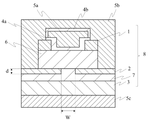
- FIG. 1 shows the main part of a metal oxide semiconductor field effect transistor (MOSFET), which is one of the preferred embodiments of the present invention.
- the MOSFET of FIG. 1 includes a drain electrode 5c, an n + type semiconductor layer 3, an n ⁇ type semiconductor layer 7 as a drift layer, a high resistance layer (current blocking region) 2, a channel layer 6, and a source region (n + type semiconductor layer) 1. , a gate insulating film 4, a gate electrode 5a and a source electrode 5b.
- the n + type semiconductor layer 3, the n ⁇ type semiconductor layer (drift layer) 7, the current blocking layer 2, the channel layer 6 and the n + type semiconductor layer ( A source layer) 1 is formed in this order.
- the n+ type semiconductor layer 3, the n ⁇ type semiconductor layer 7, the channel layer 6, the current blocking layer 2, and the n+ type semiconductor layer 1 constitute a crystalline oxide semiconductor layer 8.
- FIG. The high-resistance layer (current blocking region) 2 is formed by ion implantation and is a layer containing crystal defects due to ion implantation.
- a voltage is applied between the source electrode 5b and the drain electrode 5c, and a positive voltage is applied to the gate electrode 5a with respect to the source electrode 5b, electrons (holes) are generated. is injected into the channel layer 6 and turned on.
- the channel layer 6 is filled with a depletion layer by setting the voltage of the gate electrode to 0 V, and the transistor is turned off. Since the embodiment of the present invention uses such a high-resistance layer (current blocking region), it is possible to further improve the withstand voltage while maintaining the MOSFET operation of the semiconductor device. Further, the source electrode 5b forms a direct contact with the high resistance layer (current blocking region) 2. As shown in FIG. With such a configuration, electrons are exchanged well between the source electrode and the high resistance layer (current blocking region) 2, so that the responsiveness of the semiconductor device (MOSFET) is further improved. can be done.
- the current blocking layer overlaps the source electrode when viewed from the thickness direction of the crystalline oxide semiconductor layer 8 and overlaps a part of the channel layer when viewed in plan.
- the current blocking layer is configured so as not to partially overlap the channel layer when viewed in the thickness direction of the crystalline oxide semiconductor layer 8 .
- Such a configuration secures a current path while maintaining the current blocking effect.
- the width W of the current path is not particularly limited as long as the object of the present invention is not hindered. In an embodiment of the present invention, it is preferable that the width W of the current path is 2 ⁇ m or less, particularly when a material having a large bandgap such as gallium oxide is used for the drift layer.
- the thickness d of the current blocking layer is not particularly limited as long as the object of the present invention is not hindered.
- the thickness d of the current blocking layer is preferably 0.15 ⁇ m or more, more preferably 0.2 ⁇ m or more. It is more preferable to have
- the source region (n + -type semiconductor layer) 1 may be at least partially embedded in the channel layer 6 .
- FIG. 4 shows an example in which the source region (n + -type semiconductor layer) 1 is embedded in the channel layer 6 . According to the structure shown in FIG.
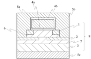
- FIG. 11 shows the main part of a metal oxide semiconductor field effect transistor (MOSFET) which is one of the preferred embodiments of the present invention.
- MOSFET metal oxide semiconductor field effect transistor
- the MOSFET of FIG. 11 differs from the MOSFET of FIG. 1 in that a high resistance layer (current blocking region) is provided on the drift layer 7 by epitaxial growth.
- each layer in FIGS. 1, 4 and 11 is not particularly limited as long as it does not hinder the object of the present invention, and may be known means. For example, after forming a film by a vacuum vapor deposition method, a CVD method, a sputtering method, or various coating techniques, a means for patterning by a photolithographic method, or a means for directly patterning using a printing technique or the like can be used.
- FIG. 2(a) shows a laminated structure in which an n+ type semiconductor layer 3 and a drift layer (n type semiconductor layer) 7 are laminated in this order on a substrate 9.
- FIG. A current blocking layer (crystal defect region) 2 is formed in the drift layer (n-type semiconductor layer) 7 of the laminate shown in FIG. 2(b) is obtained by forming the n+ type semiconductor layer 1 of FIG.
- the implantation energy of the ion implantation is not particularly limited. In an embodiment of the present invention, the implantation energy of said ion implantation is, for example, in the range of 10-500 keV.
- the n+ type semiconductor layer 1 is patterned by forming a film using an epitaxial growth method such as a mist CVD method and then etching using a known etching technique.
- a gate insulating film 4 and a gate electrode 5a are formed on the laminate shown in FIG. 2(b) to obtain the laminate shown in FIG. 2(c).
- the gate insulating film 4 and the gate electrode 5a can be processed into the shape shown in FIG. 2(c) by etching using a known etching technique after forming films using a known film forming method, respectively. can.
- the source electrode 5b is formed on the laminate shown in FIG. 2(c) using a known film formation method to obtain the laminate shown in FIG. 3(d).
- a method for forming the source electrode 5b the above-described dry method, wet method, or the like can be used.
- the semiconductor device of FIG. 3(e) can be obtained by forming the drain electrode 5c using a known film forming method.
- the semiconductor device of FIG. 3(e) has a current blocking region made up of a crystal defect region, so that the MOSFET operation (normally-off operation) is maintained and the breakdown voltage is improved.
- the effect of the electron trap density in the current blocking region of the present invention improving the withstand voltage was verified using device simulations.
- the results are shown in FIG.
- the electron trap density of the current blocking region is preferably 4 ⁇ 10 18 /cm 3 or more. With such a preferable range, the effect of improving the withstand voltage by the electron blocking region can be further promoted.
- the trap density can be measured using, for example, a DLTS (Deep Level Transient Spectroscopy) method.
- the semiconductor device according to the embodiment of the present invention described above can be applied to power converters such as inverters and converters in order to exhibit the functions described above. More specifically, it can be applied as a switching element such as a thyristor, a power transistor, an IGBT (Insulated Gate Bipolar Transistor), a MOSFET (Metal-Oxide-Semiconductor Field Effect Transistor), and the like.
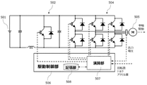
- FIG. 7 is a block configuration diagram showing an example of a control system using a semiconductor device according to an embodiment of the present invention
- FIG. 8 is a circuit diagram of the same control system, which is particularly suitable for mounting on an electric vehicle. control system.
- the control system 500 has a battery (power supply) 501, a boost converter 502, a step-down converter 503, an inverter 504, a motor (to be driven) 505, and a drive control section 506, which are mounted on an electric vehicle.
- the battery 501 is composed of a storage battery such as a nickel-metal hydride battery or a lithium-ion battery, and stores electric power by charging at a power supply station or regenerative energy during deceleration, and is necessary for the operation of the running system and electrical system of the electric vehicle. DC voltage can be output.
- the boost converter 502 is, for example, a voltage conversion device equipped with a chopper circuit, and boosts the DC voltage of, for example, 200 V supplied from the battery 501 to, for example, 650 V by the switching operation of the chopper circuit, and outputs it to a running system such as a motor. be able to.
- the step-down converter 503 is also a voltage converter equipped with a chopper circuit. It can be output to the electrical system including
- the inverter 504 converts the DC voltage supplied from the boost converter 502 into a three-phase AC voltage by switching operation, and outputs the three-phase AC voltage to the motor 505 .
- a motor 505 is a three-phase AC motor that constitutes the driving system of the electric vehicle, and is rotationally driven by the three-phase AC voltage output from the inverter 504. The rotational driving force is transmitted to the wheels of the electric vehicle via a transmission or the like (not shown). to
- various sensors are used to measure actual values such as the number of revolutions and torque of the wheels and the amount of depression of the accelerator pedal (acceleration amount) from the running electric vehicle. is entered.
- the output voltage value of inverter 504 is also input to drive control section 506 .
- the drive control unit 506 has the function of a controller equipped with a calculation unit such as a CPU (Central Processing Unit) and a data storage unit such as a memory. By outputting it as a feedback signal, the switching operation of the switching element is controlled.
- the AC voltage applied to the motor 505 by the inverter 504 is corrected instantaneously, so that the operation control of the electric vehicle can be accurately executed, and safe and comfortable operation of the electric vehicle is realized. It is also possible to control the output voltage to the inverter 504 by giving the feedback signal from the drive control unit 506 to the boost converter 502 .
- FIG. 8 is a circuit configuration excluding the step-down converter 503 in FIG. 7, that is, only a configuration for driving the motor 505.
- the semiconductor device of the present invention is employed as a Schottky barrier diode in a boost converter 502 and an inverter 504 for switching control.
- Boost converter 502 is incorporated in a chopper circuit to perform chopper control
- inverter 504 is incorporated in a switching circuit including IGBTs to perform switching control.
- An inductor (such as a coil) is interposed in the output of the battery 501 to stabilize the current. It is stabilizing the voltage.
- the drive control unit 506 is provided with an operation unit 507 made up of a CPU (Central Processing Unit) and a storage unit 508 made up of a non-volatile memory.
- a signal input to the drive control unit 506 is supplied to the calculation unit 507, and a feedback signal for each semiconductor element is generated by performing necessary calculations.
- the storage unit 508 temporarily holds the calculation result by the calculation unit 507, accumulates physical constants and functions required for drive control in the form of a table, and outputs them to the calculation unit 507 as appropriate.
- the calculation unit 507 and the storage unit 508 can employ known configurations, and their processing capabilities can be arbitrarily selected.
- switching operations of the boost converter 502, the step-down converter 503, and the inverter 504 use diodes and switching elements such as thyristors, power transistors, IGBTs, MOSFETs, and the like. .
- gallium oxide (Ga 2 O 3 ), especially corundum-type gallium oxide ( ⁇ -Ga 2 O 3 ), as the material for these semiconductor elements the switching characteristics are greatly improved. Furthermore, by applying the semiconductor device or the like according to the present invention, extremely good switching characteristics can be expected, and further miniaturization and cost reduction of the control system 500 can be realized.
- each of the boost converter 502, the step-down converter 503, and the inverter 504 can expect the effects of the present invention.
- the effect of the present invention can be expected in any of the above.
- the control system 500 described above can apply the semiconductor device of the present invention not only to the control system of an electric vehicle, but also to a control system for various purposes such as stepping up or stepping down power from a DC power supply or converting power from DC to AC. can be applied to It is also possible to use a power source such as a solar cell as the battery.
- FIG. 9 is a block configuration diagram showing another example of a control system employing a semiconductor device according to an embodiment of the present invention
- FIG. 10 is a circuit diagram of the same control system, showing infrastructure equipment that operates on power from an AC power supply. This control system is suitable for installation in home appliances, etc.
- a control system 600 receives power supplied from an external, for example, a three-phase AC power source (power source) 601, and includes an AC/DC converter 602, an inverter 604, a motor (to be driven) 605, It has a drive control unit 606, which can be mounted on various devices (described later).
- the three-phase AC power supply 601 is, for example, a power generation facility of an electric power company (a thermal power plant, a hydroelectric power plant, a geothermal power plant, a nuclear power plant, etc.), and its output is stepped down via a substation and supplied as an AC voltage. be.
- the AC/DC converter 602 is a voltage conversion device that converts AC voltage into DC voltage, and converts AC voltage of 100V or 200V supplied from the three-phase AC power supply 601 into a predetermined DC voltage. Specifically, the voltage is converted into a generally used desired DC voltage such as 3.3V, 5V, or 12V. When the object to be driven is a motor, conversion to 12V is performed.
- a single-phase AC power supply may be used instead of the three-phase AC power supply. In that case, the same system configuration can be achieved by using a single-phase input AC/DC converter.
- the inverter 604 converts the DC voltage supplied from the AC/DC converter 602 into a three-phase AC voltage by switching operation, and outputs the three-phase AC voltage to the motor 605 .
- the form of the motor 604 differs depending on the object to be controlled. When the object to be controlled is a train, the motor 604 drives the wheels. It is a three-phase AC motor, and is rotationally driven by a three-phase AC voltage output from an inverter 604, and transmits its rotational driving force to a drive target (not shown).
- the control system 600 does not require the inverter 604, and as shown in FIG. 14, the DC voltage is supplied from the AC/DC converter 602 to the driven object.
- a personal computer is supplied with a DC voltage of 3.3V
- an LED lighting device is supplied with a DC voltage of 5V.
- various sensors are used to measure actual values such as the rotation speed and torque of the driven object, or the temperature and flow rate of the surrounding environment of the driven object, and these measurement signals are input to the drive control unit 606.
- the output voltage value of inverter 604 is also input to drive control section 606 .
- drive control section 606 gives a feedback signal to inverter 604 to control the switching operation of the switching element.
- the AC voltage applied to the motor 605 by the inverter 604 is corrected instantaneously, so that the operation control of the object to be driven can be accurately executed, and the object to be driven can be operated stably.
- FIG. 10 shows the circuit configuration of FIG.
- the semiconductor device of the present invention is employed as a Schottky barrier diode in an AC/DC converter 602 and an inverter 604 for switching control.
- the AC/DC converter 602 uses, for example, a Schottky barrier diode circuit configured in a bridge shape, and performs DC conversion by converting and rectifying the negative voltage component of the input voltage into a positive voltage.
- the inverter 604 is incorporated in the switching circuit in the IGBT to perform switching control.
- a capacitor (such as an electrolytic capacitor) is interposed between the AC/DC converter 602 and the inverter 604 to stabilize the voltage.
- the driving control unit 606 is provided with an operation unit 607 made up of a CPU and a storage unit 608 made up of a non-volatile memory.
- a signal input to the drive control unit 606 is supplied to the calculation unit 607, and a feedback signal for each semiconductor element is generated by performing necessary calculations.
- the storage unit 608 also temporarily stores the results of calculations by the calculation unit 607, accumulates physical constants and functions necessary for drive control in the form of a table, and outputs them to the calculation unit 607 as appropriate.
- the calculation unit 607 and the storage unit 608 can employ known configurations, and their processing capabilities can be arbitrarily selected.
- the rectifying operation and switching operation of the AC/DC converter 602 and the inverter 604 are performed by diodes, switching elements such as thyristors and power transistors. , IGBT, MOSFET, etc. are used. Switching characteristics are improved by using gallium oxide (Ga 2 O 3 ), particularly corundum type gallium oxide ( ⁇ -Ga 2 O 3 ), as the material for these semiconductor elements. Furthermore, by applying the semiconductor film and the semiconductor device according to the present invention, extremely good switching characteristics can be expected, and further miniaturization and cost reduction of the control system 600 can be realized. That is, the AC/DC converter 602 and the inverter 604 can each be expected to have the effect of the present invention. can be expected.
- the object to be driven is not necessarily limited to those that operate mechanically, and can be applied to many devices that require AC voltage.
- the control system 600 as long as the drive object is driven by inputting power from an AC power supply, it can be applied to infrastructure equipment (for example, power equipment such as buildings and factories, communication equipment, traffic control equipment, water and sewage treatment Equipment, system equipment, labor-saving equipment, trains, etc.) and home appliances (e.g., refrigerators, washing machines, personal computers, LED lighting equipment, video equipment, audio equipment, etc.). can.
- infrastructure equipment for example, power equipment such as buildings and factories, communication equipment, traffic control equipment, water and sewage treatment Equipment, system equipment, labor-saving equipment, trains, etc.
- home appliances e.g., refrigerators, washing machines, personal computers, LED lighting equipment, video equipment, audio equipment, etc.
- the semiconductor device of the present invention can be used in various fields such as semiconductors (for example, compound semiconductor electronic devices), electronic parts/electrical equipment parts, optical/electrophotographic equipment, industrial materials, etc., but it is particularly useful for power devices. be.
Landscapes
- Crystals, And After-Treatments Of Crystals (AREA)
- Electrodes Of Semiconductors (AREA)
Abstract
Description
一方、α-Ga2O3は、既に汎用されているサファイア基板と同じ結晶構造を有するため、光・電子デバイスへの利用には好適であり、さらに、β-Ga2O3よりも広いバンドギャップをもつため、パワーデバイスに特に有用であり、そのため、α-Ga2O3を半導体として用いた半導体装置が待ち望まれている状況である。
また、本発明者らは、上記知見を得た後、さらに検討を重ねて本発明を完成させるに至った。
[1] チャネル層、ドリフト層およびソース領域を含む結晶性酸化物半導体層と、該チャネル層上にゲート絶縁膜を介して配置されているゲート電極と、前記チャネル層と前記ドリフト層との間に配置されている電流遮断領域と、前記ソース領域上に設けられているソース電極とを少なくとも備えている半導体装置であって、
前記電流遮断領域が高抵抗層からなり、前記ソース電極が、前記電流遮断領域とコンタクトを形成していることを特徴とする半導体装置。
[2] 前記ソース電極が、前記電流遮断領域と直接コンタクトしている前記[1]記載の半導体装置。
[3] 前記結晶性酸化物半導体層が、アルミニウム、インジウムおよびガリウムから選ばれる少なくとも1種の金属を含有する前記[1]または[2]に記載の半導体装置。
[4] 前記結晶性酸化物半導体層が、コランダム構造を有する前記[1]~[3]のいずれかに記載の半導体装置。
[5] 前記電流遮断領域が、ドーパントを含む前記[1]~[4]のいずれかに記載の半導体装置。
[6] 前記電流遮断領域中の前記ドーパント濃度が1.0×10¹⁷/cm3以上である前記[1]~[5]のいずれかに記載の半導体装置。
[7] 前記電流遮断領域が、イオン注入領域である前記[1]~[6]のいずれかに記載の半導体装置。
[8] 前記電流遮断領域の電子トラップ密度が、4.0×10¹⁸/cm3以上である前記[1]~[7]のいずれかに記載の半導体装置。
[9] トランジスタである前記[1]~[8]のいずれかに記載の半導体装置。
[10] 前記[1]~[9]のいずれかに記載の半導体装置を用いた電力変換装置。
[11] 前記[1]~[9]のいずれかに記載の半導体装置を用いた制御システム。
霧化工程は、前記原料溶液を霧化する。前記原料溶液の霧化手段は、前記原料溶液を霧化できさえすれば特に限定されず、公知の手段であってよいが、本発明の実施態様においては、超音波を用いる霧化手段が好ましい。超音波を用いて得られた霧化液滴は、初速度がゼロであり、空中に浮遊するので好ましく、例えば、スプレーのように吹き付けるのではなく、空間に浮遊してガスとして搬送することが可能なミストであるので衝突エネルギーによる損傷がないため、非常に好適である。液滴サイズは、特に限定されず、数mm程度の液滴であってもよいが、好ましくは50μm以下であり、より好ましくは100nm~10μmである。
前記原料溶液は、霧化または液滴化が可能であり、半導体膜を形成可能な原料を含んでいれば特に限定されず、無機材料であっても、有機材料であってもよい。本発明の実施態様においては、前記原料が、金属または金属化合物であるのが好ましく、アルミニウム、ガリウム、インジウム、鉄、クロム、バナジウム、チタン、ロジウム、ニッケル、コバルトおよびイリジウムから選ばれる1種または2種以上の金属を含むのがより好ましい。
搬送工程では、キャリアガスでもって前記霧化液滴を成膜室内に搬送する。前記キャリアガスとしては、本発明の目的を阻害しない限り特に限定されず、例えば、酸素、オゾン、窒素やアルゴン等の不活性ガス、または水素ガスやフォーミングガス等の還元ガスなどが好適な例として挙げられる。また、キャリアガスの種類は1種類であってよいが、2種類以上であってもよく、流量を下げた希釈ガス(例えば10倍希釈ガス等)などを、第2のキャリアガスとしてさらに用いてもよい。また、キャリアガスの供給箇所も1箇所だけでなく、2箇所以上あってもよい。キャリアガスの流量は、特に限定されないが、0.01~20L/分であるのが好ましく、1~10L/分であるのがより好ましい。希釈ガスの場合には、希釈ガスの流量が、0.001~2L/分であるのが好ましく、0.1~1L/分であるのがより好ましい。
成膜工程では、前記基体近傍で前記霧化液滴を熱反応させることによって、基体上に、前記半導体膜を成膜する。熱反応は、熱でもって前記霧化液滴が反応すればそれでよく、反応条件等も本発明の目的を阻害しない限り特に限定されない。本工程においては、前記熱反応を、通常、溶媒の蒸発温度以上の温度で行うが、高すぎない温度(例えば1000℃)以下が好ましく、650℃以下がより好ましく、300℃~650℃が最も好ましい。また、熱反応は、本発明の目的を阻害しない限り、真空下、非酸素雰囲気下(例えば、不活性ガス雰囲気下等)、還元ガス雰囲気下および酸素雰囲気下のいずれの雰囲気下で行われてもよいが、不活性ガス雰囲気下または酸素雰囲気下で行われるのが好ましい。また、大気圧下、加圧下および減圧下のいずれの条件下で行われてもよいが、本発明の実施態様においては、大気圧下で行われるのが好ましい。なお、膜厚は、成膜時間を調整することにより、設定することができる。
前記基体は、前記半導体膜を支持できるものであれば特に限定されない。前記基体の材料も、本発明の目的を阻害しない限り特に限定されず、公知の基体であってよく、有機化合物であってもよいし、無機化合物であってもよい。前記基体の形状としては、どのような形状のものであってもよく、あらゆる形状に対して有効であり、例えば、平板や円板等の板状、繊維状、棒状、円柱状、角柱状、筒状、螺旋状、球状、リング状などが挙げられるが、本発明の実施態様においては、基板が好ましい。基板の厚さは、本発明の実施態様においては特に限定されない。
なお、上述の制御システム500は本発明の半導体装置を電気自動車の制御システムに適用できるだけではなく、直流電源からの電力を昇圧・降圧したり、直流から交流へ電力変換するといったあらゆる用途の制御システムに適用することが可能である。また、バッテリーとして太陽電池などの電源を用いることも可能である。
2 高抵抗層(電流遮断領域)
3 n-型半導体層
4a ゲート絶縁膜
4b 層間絶縁膜
5a ゲート電極
5b ソース電極
5c ドレイン電極
6 チャネル層
7 n-型半導体層
8 結晶性酸化物半導体層
9 基板
21 成膜装置(ミストCVD装置)
22a キャリアガス源
22b キャリアガス(希釈)源
23a 流量調節弁
23b 流量調節弁
24 ミスト発生源
24a 原料溶液
24b 原料微粒子
25 容器
25a 水
26 超音波振動子
27 成膜室
28 ホットプレート
29 供給管
30 基板
500 制御システム
501 バッテリー(電源)
502 昇圧コンバータ
503 降圧コンバータ
504 インバータ
505 モータ(駆動対象)
506 駆動制御部
507 演算部
508 記憶部
600 制御システム
601 三相交流電源(電源)
602 AC/DCコンバータ
604 インバータ
605 モータ(駆動対象)
606 駆動制御部
607 演算部
608 記憶部
Claims (11)
- チャネル層、ドリフト層およびソース領域を含む結晶性酸化物半導体層と、該チャネル層上にゲート絶縁膜を介して配置されているゲート電極と、前記チャネル層と前記ドリフト層との間に配置されている電流遮断領域と、前記ソース領域上に設けられているソース電極とを少なくとも備えている半導体装置であって、
前記電流遮断領域が高抵抗層からなり、前記ソース電極が、前記電流遮断領域とコンタクトを形成していることを特徴とする半導体装置。 - 前記ソース電極が、前記電流遮断領域と直接コンタクトしている請求項1記載の半導体装置。
- 前記結晶性酸化物半導体層が、アルミニウム、インジウムおよびガリウムから選ばれる少なくとも1種の金属を含有する請求項1または2に記載の半導体装置。
- 前記結晶性酸化物半導体層が、コランダム構造を有する請求項1~3のいずれかに記載の半導体装置。
- 前記電流遮断領域が、ドーパントを含む請求項1~4のいずれかに記載の半導体装置。
- 前記電流遮断領域中の前記ドーパント濃度が1.0×10¹⁷/cm3以上である請求項5記載の半導体装置。
- 前記電流遮断領域が、イオン注入領域である請求項1~6のいずれかに記載の半導体装置。
- 前記電流遮断領域の電子トラップ密度が、4.0×10¹⁸/cm3以上である請求項1~7のいずれかに記載の半導体装置。
- トランジスタである請求項1~8のいずれかに記載の半導体装置。
- 請求項1~9のいずれかに記載の半導体装置を用いた電力変換装置。
- 請求項1~9のいずれかに記載の半導体装置を用いた制御システム。
Priority Applications (4)
| Application Number | Priority Date | Filing Date | Title |
|---|---|---|---|
| JP2023517525A JPWO2022230832A1 (ja) | 2021-04-26 | 2022-04-25 | |
| CN202280031272.0A CN117223111A (zh) | 2021-04-26 | 2022-04-25 | 半导体装置 |
| EP22795745.3A EP4333076A4 (en) | 2021-04-26 | 2022-04-25 | SEMICONDUCTOR ARRANGEMENT |
| US18/384,121 US20240055510A1 (en) | 2021-04-26 | 2023-10-26 | Semiconductor device |
Applications Claiming Priority (2)
| Application Number | Priority Date | Filing Date | Title |
|---|---|---|---|
| JP2021-074520 | 2021-04-26 | ||
| JP2021074520 | 2021-04-26 |
Related Child Applications (1)
| Application Number | Title | Priority Date | Filing Date |
|---|---|---|---|
| US18/384,121 Continuation-In-Part US20240055510A1 (en) | 2021-04-26 | 2023-10-26 | Semiconductor device |
Publications (1)
| Publication Number | Publication Date |
|---|---|
| WO2022230832A1 true WO2022230832A1 (ja) | 2022-11-03 |
Family
ID=83848096
Family Applications (1)
| Application Number | Title | Priority Date | Filing Date |
|---|---|---|---|
| PCT/JP2022/018788 Ceased WO2022230832A1 (ja) | 2021-04-26 | 2022-04-25 | 半導体装置 |
Country Status (5)
| Country | Link |
|---|---|
| US (1) | US20240055510A1 (ja) |
| EP (1) | EP4333076A4 (ja) |
| JP (1) | JPWO2022230832A1 (ja) |
| CN (1) | CN117223111A (ja) |
| WO (1) | WO2022230832A1 (ja) |
Citations (2)
| Publication number | Priority date | Publication date | Assignee | Title |
|---|---|---|---|---|
| JP2018060992A (ja) * | 2015-12-18 | 2018-04-12 | 株式会社Flosfia | 半導体装置 |
| JP2018186246A (ja) | 2017-04-27 | 2018-11-22 | 国立研究開発法人情報通信研究機構 | Ga2O3系半導体素子 |
Family Cites Families (13)
| Publication number | Priority date | Publication date | Assignee | Title |
|---|---|---|---|---|
| JP4858791B2 (ja) * | 2009-05-22 | 2012-01-18 | 住友電気工業株式会社 | 半導体装置およびその製造方法 |
| US10367089B2 (en) * | 2011-03-28 | 2019-07-30 | General Electric Company | Semiconductor device and method for reduced bias threshold instability |
| JP2013235895A (ja) * | 2012-05-07 | 2013-11-21 | Sumitomo Electric Ind Ltd | 半導体装置およびその製造方法 |
| US10573722B2 (en) * | 2016-02-17 | 2020-02-25 | General Electric Company | Systems and methods for in-situ doped semiconductor gate electrodes for wide bandgap semiconductor power devices |
| US10636663B2 (en) * | 2017-03-29 | 2020-04-28 | Toyoda Gosei Co., Ltd. | Method of manufacturing semiconductor device including implanting impurities into an implanted region of a semiconductor layer and annealing the implanted region |
| WO2019066966A1 (en) * | 2017-09-29 | 2019-04-04 | Intel Corporation | CMOS CIRCUIT WITH A GROUP III NITRIDE TRANSISTOR AND ITS SUPPLY METHOD |
| US11264512B2 (en) * | 2018-06-29 | 2022-03-01 | Intel Corporation | Thin film transistors having U-shaped features |
| US11527656B2 (en) * | 2018-09-25 | 2022-12-13 | Intel Corporation | Contact electrodes for vertical thin-film transistors |
| JP6857641B2 (ja) * | 2018-12-19 | 2021-04-14 | 信越化学工業株式会社 | 成膜方法及び成膜装置 |
| US10847647B2 (en) * | 2019-03-14 | 2020-11-24 | Cree, Inc. | Power semiconductor devices having top-side metallization structures that include buried grain stop layers |
| US11888034B2 (en) * | 2019-06-07 | 2024-01-30 | Intel Corporation | Transistors with metal chalcogenide channel materials |
| US11171239B2 (en) * | 2019-09-13 | 2021-11-09 | Intel Corporation | Transistor channel passivation with 2D crystalline material |
| US20230006049A1 (en) * | 2021-06-30 | 2023-01-05 | Hunan Sanan Semiconductor Co., Ltd. | Silicon carbide power device with an enhanced junction field effect transistor region |
-
2022
- 2022-04-25 WO PCT/JP2022/018788 patent/WO2022230832A1/ja not_active Ceased
- 2022-04-25 JP JP2023517525A patent/JPWO2022230832A1/ja active Pending
- 2022-04-25 CN CN202280031272.0A patent/CN117223111A/zh active Pending
- 2022-04-25 EP EP22795745.3A patent/EP4333076A4/en active Pending
-
2023
- 2023-10-26 US US18/384,121 patent/US20240055510A1/en active Pending
Patent Citations (2)
| Publication number | Priority date | Publication date | Assignee | Title |
|---|---|---|---|---|
| JP2018060992A (ja) * | 2015-12-18 | 2018-04-12 | 株式会社Flosfia | 半導体装置 |
| JP2018186246A (ja) | 2017-04-27 | 2018-11-22 | 国立研究開発法人情報通信研究機構 | Ga2O3系半導体素子 |
Non-Patent Citations (3)
| Title |
|---|
| HIGASHIWAKI MASATAKA; WONG MAN HOI; KONISHI KEITA; NAKATA YOSHIAKI; LIN CHIA-HUNG; KAMIMURA TAKAFUMI; RAVIKIRAN LINGAPARTHI; SASAK: "Latest progress in gallium-oxide electronic devices", PROCEEDINGS OF SPIE, vol. 10533, 23 February 2018 (2018-02-23), US , pages 1 - 6, XP060102914, ISBN: 978-1-5106-1533-5, DOI: 10.1117/12.2292666 * |
| See also references of EP4333076A4 |
| WONG MAN HOI; MURAKAMI HISASHI; KUMAGAI YOSHINAO; HIGASHIWAKI MASATAKA: "Enhancement-Mode $\beta$ -Ga2O3 Current Aperture Vertical MOSFETs With N-Ion-Implanted Blocker", IEEE ELECTRON DEVICE LETTERS, vol. 41, no. 2, 26 December 2019 (2019-12-26), USA, pages 296 - 299, XP011768906, ISSN: 0741-3106, DOI: 10.1109/LED.2019.2962657 * |
Also Published As
| Publication number | Publication date |
|---|---|
| US20240055510A1 (en) | 2024-02-15 |
| CN117223111A (zh) | 2023-12-12 |
| JPWO2022230832A1 (ja) | 2022-11-03 |
| EP4333076A1 (en) | 2024-03-06 |
| EP4333076A4 (en) | 2025-05-07 |
Similar Documents
| Publication | Publication Date | Title |
|---|---|---|
| US12289917B2 (en) | Semiconductor device | |
| WO2022230830A1 (ja) | 半導体装置 | |
| WO2023008454A1 (ja) | 結晶性酸化物膜および半導体装置 | |
| US20240055471A1 (en) | Semiconductor device | |
| US11855135B2 (en) | Semiconductor device | |
| CN116114061A (zh) | 半导体元件及半导体装置 | |
| US20240363695A1 (en) | Semiconductor device | |
| KR102870633B1 (ko) | 반도체 장치 | |
| JP2022187481A (ja) | 半導体装置 | |
| JP7823289B2 (ja) | 半導体素子および半導体装置 | |
| WO2022230832A1 (ja) | 半導体装置 | |
| WO2022230834A1 (ja) | 半導体装置 | |
| TWI915548B (zh) | 半導體裝置、電力轉換裝置及控制系統 | |
| WO2023008452A1 (ja) | 酸化物半導体および半導体装置 | |
| WO2022210615A1 (ja) | 半導体装置 | |
| JP2022187480A (ja) | 半導体装置 | |
| JP2022011781A (ja) | 結晶性酸化物膜および半導体装置 | |
| WO2023145912A1 (ja) | 積層構造体、半導体素子および半導体装置 | |
| WO2023145910A1 (ja) | 積層構造体、半導体素子および半導体装置 | |
| WO2023145911A1 (ja) | 積層構造体、半導体素子および半導体装置 |
Legal Events
| Date | Code | Title | Description |
|---|---|---|---|
| 121 | Ep: the epo has been informed by wipo that ep was designated in this application |
Ref document number: 22795745 Country of ref document: EP Kind code of ref document: A1 |
|
| WWE | Wipo information: entry into national phase |
Ref document number: 2023517525 Country of ref document: JP |
|
| WWE | Wipo information: entry into national phase |
Ref document number: 202280031272.0 Country of ref document: CN |
|
| WWE | Wipo information: entry into national phase |
Ref document number: 2022795745 Country of ref document: EP |
|
| NENP | Non-entry into the national phase |
Ref country code: DE |
|
| ENP | Entry into the national phase |
Ref document number: 2022795745 Country of ref document: EP Effective date: 20231127 |